WO2018203169A1 - 撮像装置、及び電子機器 - Google Patents
撮像装置、及び電子機器 Download PDFInfo
- Publication number
- WO2018203169A1 WO2018203169A1 PCT/IB2018/052743 IB2018052743W WO2018203169A1 WO 2018203169 A1 WO2018203169 A1 WO 2018203169A1 IB 2018052743 W IB2018052743 W IB 2018052743W WO 2018203169 A1 WO2018203169 A1 WO 2018203169A1
- Authority
- WO
- WIPO (PCT)
- Prior art keywords
- circuit
- transistor
- wiring
- insulator
- conductor
- Prior art date
- Legal status (The legal status is an assumption and is not a legal conclusion. Google has not performed a legal analysis and makes no representation as to the accuracy of the status listed.)
- Ceased
Links
Images

















Classifications
-
- H—ELECTRICITY
- H10—SEMICONDUCTOR DEVICES; ELECTRIC SOLID-STATE DEVICES NOT OTHERWISE PROVIDED FOR
- H10F—INORGANIC SEMICONDUCTOR DEVICES SENSITIVE TO INFRARED RADIATION, LIGHT, ELECTROMAGNETIC RADIATION OF SHORTER WAVELENGTH OR CORPUSCULAR RADIATION
- H10F39/00—Integrated devices, or assemblies of multiple devices, comprising at least one element covered by group H10F30/00, e.g. radiation detectors comprising photodiode arrays
- H10F39/80—Constructional details of image sensors
- H10F39/803—Pixels having integrated switching, control, storage or amplification elements
-
- G—PHYSICS
- G06—COMPUTING OR CALCULATING; COUNTING
- G06N—COMPUTING ARRANGEMENTS BASED ON SPECIFIC COMPUTATIONAL MODELS
- G06N3/00—Computing arrangements based on biological models
- G06N3/02—Neural networks
- G06N3/04—Architecture, e.g. interconnection topology
- G06N3/045—Combinations of networks
-
- G—PHYSICS
- G06—COMPUTING OR CALCULATING; COUNTING
- G06N—COMPUTING ARRANGEMENTS BASED ON SPECIFIC COMPUTATIONAL MODELS
- G06N3/00—Computing arrangements based on biological models
- G06N3/02—Neural networks
- G06N3/04—Architecture, e.g. interconnection topology
- G06N3/045—Combinations of networks
- G06N3/0455—Auto-encoder networks; Encoder-decoder networks
-
- G—PHYSICS
- G06—COMPUTING OR CALCULATING; COUNTING
- G06N—COMPUTING ARRANGEMENTS BASED ON SPECIFIC COMPUTATIONAL MODELS
- G06N3/00—Computing arrangements based on biological models
- G06N3/02—Neural networks
- G06N3/04—Architecture, e.g. interconnection topology
- G06N3/0464—Convolutional networks [CNN, ConvNet]
-
- G—PHYSICS
- G06—COMPUTING OR CALCULATING; COUNTING
- G06N—COMPUTING ARRANGEMENTS BASED ON SPECIFIC COMPUTATIONAL MODELS
- G06N3/00—Computing arrangements based on biological models
- G06N3/02—Neural networks
- G06N3/06—Physical realisation, i.e. hardware implementation of neural networks, neurons or parts of neurons
- G06N3/063—Physical realisation, i.e. hardware implementation of neural networks, neurons or parts of neurons using electronic means
- G06N3/065—Analogue means
-
- G—PHYSICS
- G06—COMPUTING OR CALCULATING; COUNTING
- G06N—COMPUTING ARRANGEMENTS BASED ON SPECIFIC COMPUTATIONAL MODELS
- G06N3/00—Computing arrangements based on biological models
- G06N3/02—Neural networks
- G06N3/08—Learning methods
- G06N3/088—Non-supervised learning, e.g. competitive learning
-
- G—PHYSICS
- G06—COMPUTING OR CALCULATING; COUNTING
- G06N—COMPUTING ARRANGEMENTS BASED ON SPECIFIC COMPUTATIONAL MODELS
- G06N3/00—Computing arrangements based on biological models
- G06N3/02—Neural networks
- G06N3/08—Learning methods
- G06N3/09—Supervised learning
-
- G—PHYSICS
- G06—COMPUTING OR CALCULATING; COUNTING
- G06V—IMAGE OR VIDEO RECOGNITION OR UNDERSTANDING
- G06V10/00—Arrangements for image or video recognition or understanding
- G06V10/40—Extraction of image or video features
- G06V10/44—Local feature extraction by analysis of parts of the pattern, e.g. by detecting edges, contours, loops, corners, strokes or intersections; Connectivity analysis, e.g. of connected components
- G06V10/443—Local feature extraction by analysis of parts of the pattern, e.g. by detecting edges, contours, loops, corners, strokes or intersections; Connectivity analysis, e.g. of connected components by matching or filtering
- G06V10/449—Biologically inspired filters, e.g. difference of Gaussians [DoG] or Gabor filters
- G06V10/451—Biologically inspired filters, e.g. difference of Gaussians [DoG] or Gabor filters with interaction between the filter responses, e.g. cortical complex cells
- G06V10/454—Integrating the filters into a hierarchical structure, e.g. convolutional neural networks [CNN]
-
- H—ELECTRICITY
- H04—ELECTRIC COMMUNICATION TECHNIQUE
- H04N—PICTORIAL COMMUNICATION, e.g. TELEVISION
- H04N25/00—Circuitry of solid-state image sensors [SSIS]; Control thereof
-
- H—ELECTRICITY
- H04—ELECTRIC COMMUNICATION TECHNIQUE
- H04N—PICTORIAL COMMUNICATION, e.g. TELEVISION
- H04N25/00—Circuitry of solid-state image sensors [SSIS]; Control thereof
- H04N25/70—SSIS architectures; Circuits associated therewith
- H04N25/76—Addressed sensors, e.g. MOS or CMOS sensors
-
- H—ELECTRICITY
- H04—ELECTRIC COMMUNICATION TECHNIQUE
- H04N—PICTORIAL COMMUNICATION, e.g. TELEVISION
- H04N25/00—Circuitry of solid-state image sensors [SSIS]; Control thereof
- H04N25/70—SSIS architectures; Circuits associated therewith
- H04N25/76—Addressed sensors, e.g. MOS or CMOS sensors
- H04N25/78—Readout circuits for addressed sensors, e.g. output amplifiers or A/D converters
-
- H—ELECTRICITY
- H04—ELECTRIC COMMUNICATION TECHNIQUE
- H04N—PICTORIAL COMMUNICATION, e.g. TELEVISION
- H04N25/00—Circuitry of solid-state image sensors [SSIS]; Control thereof
- H04N25/70—SSIS architectures; Circuits associated therewith
- H04N25/79—Arrangements of circuitry being divided between different or multiple substrates, chips or circuit boards, e.g. stacked image sensors
-
- H—ELECTRICITY
- H10—SEMICONDUCTOR DEVICES; ELECTRIC SOLID-STATE DEVICES NOT OTHERWISE PROVIDED FOR
- H10B—ELECTRONIC MEMORY DEVICES
- H10B99/00—Subject matter not provided for in other groups of this subclass
- H10B99/22—Subject matter not provided for in other groups of this subclass including field-effect components
-
- H—ELECTRICITY
- H10—SEMICONDUCTOR DEVICES; ELECTRIC SOLID-STATE DEVICES NOT OTHERWISE PROVIDED FOR
- H10D—INORGANIC ELECTRIC SEMICONDUCTOR DEVICES
- H10D30/00—Field-effect transistors [FET]
- H10D30/60—Insulated-gate field-effect transistors [IGFET]
- H10D30/67—Thin-film transistors [TFT]
- H10D30/674—Thin-film transistors [TFT] characterised by the active materials
- H10D30/6755—Oxide semiconductors, e.g. zinc oxide, copper aluminium oxide or cadmium stannate
-
- H—ELECTRICITY
- H10—SEMICONDUCTOR DEVICES; ELECTRIC SOLID-STATE DEVICES NOT OTHERWISE PROVIDED FOR
- H10D—INORGANIC ELECTRIC SEMICONDUCTOR DEVICES
- H10D86/00—Integrated devices formed in or on insulating or conducting substrates, e.g. formed in silicon-on-insulator [SOI] substrates or on stainless steel or glass substrates
- H10D86/201—Integrated devices formed in or on insulating or conducting substrates, e.g. formed in silicon-on-insulator [SOI] substrates or on stainless steel or glass substrates the substrates comprising an insulating layer on a semiconductor body, e.g. SOI
- H10D86/215—Integrated devices formed in or on insulating or conducting substrates, e.g. formed in silicon-on-insulator [SOI] substrates or on stainless steel or glass substrates the substrates comprising an insulating layer on a semiconductor body, e.g. SOI comprising FinFETs
-
- H—ELECTRICITY
- H10—SEMICONDUCTOR DEVICES; ELECTRIC SOLID-STATE DEVICES NOT OTHERWISE PROVIDED FOR
- H10D—INORGANIC ELECTRIC SEMICONDUCTOR DEVICES
- H10D86/00—Integrated devices formed in or on insulating or conducting substrates, e.g. formed in silicon-on-insulator [SOI] substrates or on stainless steel or glass substrates
- H10D86/40—Integrated devices formed in or on insulating or conducting substrates, e.g. formed in silicon-on-insulator [SOI] substrates or on stainless steel or glass substrates characterised by multiple TFTs
- H10D86/421—Integrated devices formed in or on insulating or conducting substrates, e.g. formed in silicon-on-insulator [SOI] substrates or on stainless steel or glass substrates characterised by multiple TFTs having a particular composition, shape or crystalline structure of the active layer
- H10D86/423—Integrated devices formed in or on insulating or conducting substrates, e.g. formed in silicon-on-insulator [SOI] substrates or on stainless steel or glass substrates characterised by multiple TFTs having a particular composition, shape or crystalline structure of the active layer comprising semiconductor materials not belonging to the Group IV, e.g. InGaZnO
-
- H—ELECTRICITY
- H10—SEMICONDUCTOR DEVICES; ELECTRIC SOLID-STATE DEVICES NOT OTHERWISE PROVIDED FOR
- H10D—INORGANIC ELECTRIC SEMICONDUCTOR DEVICES
- H10D86/00—Integrated devices formed in or on insulating or conducting substrates, e.g. formed in silicon-on-insulator [SOI] substrates or on stainless steel or glass substrates
- H10D86/40—Integrated devices formed in or on insulating or conducting substrates, e.g. formed in silicon-on-insulator [SOI] substrates or on stainless steel or glass substrates characterised by multiple TFTs
- H10D86/441—Interconnections, e.g. scanning lines
-
- H—ELECTRICITY
- H10—SEMICONDUCTOR DEVICES; ELECTRIC SOLID-STATE DEVICES NOT OTHERWISE PROVIDED FOR
- H10D—INORGANIC ELECTRIC SEMICONDUCTOR DEVICES
- H10D86/00—Integrated devices formed in or on insulating or conducting substrates, e.g. formed in silicon-on-insulator [SOI] substrates or on stainless steel or glass substrates
- H10D86/40—Integrated devices formed in or on insulating or conducting substrates, e.g. formed in silicon-on-insulator [SOI] substrates or on stainless steel or glass substrates characterised by multiple TFTs
- H10D86/481—Integrated devices formed in or on insulating or conducting substrates, e.g. formed in silicon-on-insulator [SOI] substrates or on stainless steel or glass substrates characterised by multiple TFTs integrated with passive devices, e.g. auxiliary capacitors
-
- H—ELECTRICITY
- H10—SEMICONDUCTOR DEVICES; ELECTRIC SOLID-STATE DEVICES NOT OTHERWISE PROVIDED FOR
- H10D—INORGANIC ELECTRIC SEMICONDUCTOR DEVICES
- H10D86/00—Integrated devices formed in or on insulating or conducting substrates, e.g. formed in silicon-on-insulator [SOI] substrates or on stainless steel or glass substrates
- H10D86/40—Integrated devices formed in or on insulating or conducting substrates, e.g. formed in silicon-on-insulator [SOI] substrates or on stainless steel or glass substrates characterised by multiple TFTs
- H10D86/60—Integrated devices formed in or on insulating or conducting substrates, e.g. formed in silicon-on-insulator [SOI] substrates or on stainless steel or glass substrates characterised by multiple TFTs wherein the TFTs are in active matrices
-
- H—ELECTRICITY
- H10—SEMICONDUCTOR DEVICES; ELECTRIC SOLID-STATE DEVICES NOT OTHERWISE PROVIDED FOR
- H10D—INORGANIC ELECTRIC SEMICONDUCTOR DEVICES
- H10D87/00—Integrated devices comprising both bulk components and either SOI or SOS components on the same substrate
-
- H—ELECTRICITY
- H10—SEMICONDUCTOR DEVICES; ELECTRIC SOLID-STATE DEVICES NOT OTHERWISE PROVIDED FOR
- H10F—INORGANIC SEMICONDUCTOR DEVICES SENSITIVE TO INFRARED RADIATION, LIGHT, ELECTROMAGNETIC RADIATION OF SHORTER WAVELENGTH OR CORPUSCULAR RADIATION
- H10F39/00—Integrated devices, or assemblies of multiple devices, comprising at least one element covered by group H10F30/00, e.g. radiation detectors comprising photodiode arrays
- H10F39/80—Constructional details of image sensors
- H10F39/805—Coatings
- H10F39/8053—Colour filters
-
- H—ELECTRICITY
- H10—SEMICONDUCTOR DEVICES; ELECTRIC SOLID-STATE DEVICES NOT OTHERWISE PROVIDED FOR
- H10F—INORGANIC SEMICONDUCTOR DEVICES SENSITIVE TO INFRARED RADIATION, LIGHT, ELECTROMAGNETIC RADIATION OF SHORTER WAVELENGTH OR CORPUSCULAR RADIATION
- H10F39/00—Integrated devices, or assemblies of multiple devices, comprising at least one element covered by group H10F30/00, e.g. radiation detectors comprising photodiode arrays
- H10F39/80—Constructional details of image sensors
- H10F39/806—Optical elements or arrangements associated with the image sensors
- H10F39/8063—Microlenses
-
- H—ELECTRICITY
- H10—SEMICONDUCTOR DEVICES; ELECTRIC SOLID-STATE DEVICES NOT OTHERWISE PROVIDED FOR
- H10F—INORGANIC SEMICONDUCTOR DEVICES SENSITIVE TO INFRARED RADIATION, LIGHT, ELECTROMAGNETIC RADIATION OF SHORTER WAVELENGTH OR CORPUSCULAR RADIATION
- H10F39/00—Integrated devices, or assemblies of multiple devices, comprising at least one element covered by group H10F30/00, e.g. radiation detectors comprising photodiode arrays
- H10F39/80—Constructional details of image sensors
- H10F39/811—Interconnections
-
- G—PHYSICS
- G06—COMPUTING OR CALCULATING; COUNTING
- G06N—COMPUTING ARRANGEMENTS BASED ON SPECIFIC COMPUTATIONAL MODELS
- G06N3/00—Computing arrangements based on biological models
- G06N3/02—Neural networks
- G06N3/08—Learning methods
- G06N3/084—Backpropagation, e.g. using gradient descent
-
- H—ELECTRICITY
- H10—SEMICONDUCTOR DEVICES; ELECTRIC SOLID-STATE DEVICES NOT OTHERWISE PROVIDED FOR
- H10D—INORGANIC ELECTRIC SEMICONDUCTOR DEVICES
- H10D30/00—Field-effect transistors [FET]
- H10D30/60—Insulated-gate field-effect transistors [IGFET]
- H10D30/67—Thin-film transistors [TFT]
- H10D30/6729—Thin-film transistors [TFT] characterised by the electrodes
- H10D30/673—Thin-film transistors [TFT] characterised by the electrodes characterised by the shapes, relative sizes or dispositions of the gate electrodes
- H10D30/6733—Multi-gate TFTs
- H10D30/6734—Multi-gate TFTs having gate electrodes arranged on both top and bottom sides of the channel, e.g. dual-gate TFTs
Definitions
- One embodiment of the present invention relates to an imaging device and an electronic device.
- one embodiment of the present invention is not limited to the above technical field.
- the technical field of the invention disclosed in this specification and the like relates to an object, a method, or a manufacturing method.
- one embodiment of the present invention relates to a process, a machine, a manufacture, or a composition (composition of matter). Therefore, the technical field of one embodiment of the present invention disclosed in this specification more specifically includes a semiconductor device, a display device, a liquid crystal display device, a light-emitting device, a power storage device, an imaging device, a memory device, a processor, an electronic device,
- the driving method, the manufacturing method, the inspection method, or the system thereof can be given as an example.
- Patent Document 1 discloses an imaging device having a structure in which a transistor including an oxide semiconductor is used for a pixel circuit.
- An artificial neural network is an information processing system that uses a neural network as a model, and it is expected that a computer with higher performance than a conventional Neumann computer can be realized by using the artificial neural network.
- Patent Document 2 discloses an invention in which weight data used for calculation of an artificial neural network is held by a memory device using a transistor having an oxide semiconductor in a channel formation region.
- the data capacity of the acquired image data tends to increase as the display device becomes higher in definition.
- An object of one embodiment of the present invention is to provide a novel imaging device. Another object of one embodiment of the present invention is to provide an electronic device including a novel imaging device.
- problems of one embodiment of the present invention are not limited to the problems listed above.
- the problems listed above do not disturb the existence of other problems.
- Other issues are issues not mentioned in this section, which are described in the following description. Problems not mentioned in this item can be derived from descriptions of the specification or drawings by those skilled in the art, and can be appropriately extracted from these descriptions.
- one embodiment of the present invention solves at least one of the above-described problems and other problems. Note that one embodiment of the present invention does not have to solve all of the problems listed above and other problems.
- One embodiment of the present invention is an imaging device including an imaging unit and an encoder, and the imaging unit has a function of generating first image data by imaging, and the encoder constitutes a first neural network.
- the image pickup apparatus includes a first circuit, and the first circuit has a function of generating second image data by performing feature extraction on the first image data using a first neural network.
- the first neural network is an imaging device having a function of performing a convolution process using a weighting filter.
- the encoder includes a shift register, the encoder includes a memory cell array, and the input terminal of the shift register is electrically connected to the imaging portion.
- the output terminal of the register is electrically connected to the memory cell array, the memory cell array has a function of storing the filter value of the weight filter, and the shift register sequentially stores the first image data for each pixel area of the imaging unit.
- the imaging apparatus has a function of outputting to a cell array, and the convolution processing includes a product-sum operation using first image data and a filter value.
- the imaging unit includes pixels of n rows and m columns (n and m are integers of 1 or more), and the imaging unit captures images.
- the pixel area has a function of generating the first image data by acquiring the pixel data according to, and the pixel region has t rows and s columns (t is an integer of 1 to n, and s is 1 to m.
- the shift register has t ⁇ m stages of holding circuits, and the shift register outputs t ⁇ s pixel data included in the pixel area to the memory cell array in a batch. It is an imaging device characterized by having the function to perform.
- the memory cell array includes a first transistor, and the first transistor includes a metal oxide in a channel formation region. It is the imaging device characterized.
- one embodiment of the present invention is an electronic device including the imaging device according to any one of (1) to (5) and a decoder, and the decoder configures a second neural network.
- the second circuit is electrically connected to the first circuit, and the second circuit performs a restoration process by the second neural network on the second image data to generate the third image data. It is an electronic device characterized by having a function to perform.
- Another embodiment of the present invention is an electronic device including the display device in the structure described in (6).
- a novel imaging device can be provided.
- an electronic device including a novel imaging device can be provided.
- an imaging device with a small circuit area can be provided.
- an imaging device with reduced power consumption can be provided.
- the effects of one embodiment of the present invention are not limited to the effects listed above.
- the effects listed above do not preclude the existence of other effects.
- the other effects are effects not mentioned in this item described in the following description. Effects not mentioned in this item can be derived from the description of the specification or drawings by those skilled in the art, and can be appropriately extracted from these descriptions.
- one embodiment of the present invention has at least one of the effects listed above and other effects. Accordingly, one embodiment of the present invention may not have the above-described effects depending on circumstances.
- FIG. 11 is a block diagram illustrating a configuration example of an electronic device.
- the block diagram which shows the structural example of a circuit.
- the figure which shows the structural example of CNN The figure which shows the structural example of a pixel and a filter.
- the figure which shows the example of a convolution process The figure which shows the example of a convolution process.
- the figure which shows the structural example of a feature map The figure which shows an example of a circuit.
- the figure which shows an example of a circuit The figure which shows an example of a circuit.
- the figure which shows an example of a circuit The figure which shows an example of a circuit.
- the figure which shows an example of a circuit The figure which shows an example of a hierarchical artificial neural network.
- the figure which shows an example of a hierarchical artificial neural network The figure which shows an example of a hierarchical artificial neural network.
- the figure which shows an example of a hierarchical artificial neural network The figure which shows an example of a hierarchical artificial neural network.
- FIG. 10A and 10B each illustrate a configuration example of a circuit.
- the block diagram which shows the structural example of a circuit.
- the block diagram and circuit diagram which show the structural example of a product-sum operation circuit.
- the block diagram and circuit diagram explaining a programmable switch.
- the block diagram which shows the structural example of a circuit.
- the block diagram which shows the structural example of a circuit.
- the block diagram which shows the structural example of a circuit.
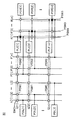
- the block diagram which shows the structural example of a circuit The block diagram which shows the structural example of a product-sum operation circuit.
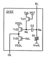
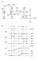
- the circuit diagram which shows the structural example of the circuit which a product-sum operation circuit has.
- the timing chart which shows the operation example of a product-sum operation circuit.
- FIG. 10 is a cross-sectional view illustrating a structure example of a semiconductor device.
- FIG. 10 is a cross-sectional view illustrating a structure example of a semiconductor device.
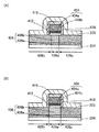
- 10A and 10B are a top view and a cross-sectional view illustrating a structure example of a transistor.
- FIG. 10 is a cross-sectional view illustrating a structural example of a transistor.
- 10A and 10B are a top view and a cross-sectional view illustrating a structure example of a transistor.
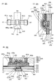
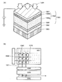
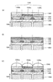
- Sectional drawing which shows the structure of an imaging device.
- FIG. 9 illustrates a configuration example of an electronic device.
- an artificial neural network refers to all models that mimic biological neural networks.
- a neural network has a configuration in which units simulating neurons are connected to each other via units simulating synapses.
- the strength of synapse connection (also called the connection strength between neurons or the weighting factor) can be changed by giving existing information to the neural network. In this way, the process of giving existing information to the neural network and determining the coupling strength is sometimes called “learning”.
- new information can be output based on the connection strength by giving some information to the neural network that has been “learned” (the connection strength is determined).
- the connection strength is determined.
- a process of outputting new information based on given information and connection strength may be referred to as “inference” or “cognition”.
- Examples of neural network models include a hop field type and a hierarchical type.
- a neural network having a multilayer structure is referred to as “deep neural network” (DNN), and machine learning by the deep neural network is referred to as “deep learning”.
- DNN deep neural network
- a metal oxide is a metal oxide in a broad expression.
- Metal oxides are classified into oxide insulators, oxide conductors (including transparent oxide conductors), oxide semiconductors (also referred to as oxide semiconductors or simply OS), and the like.
- the metal oxide may be referred to as an oxide semiconductor.
- the metal oxide in the case where a metal oxide can form a channel formation region of a transistor having at least one of an amplifying function, a rectifying function, and a switching function, the metal oxide is abbreviated as a metal oxide semiconductor (metal oxide semiconductor). It can be called OS.
- OS FET or an OS transistor
- it can be referred to as a transistor including a metal oxide or an oxide semiconductor.
- FIG. 1 is a block diagram illustrating a configuration example of an electronic device which is one embodiment of the present invention.
- the electronic device 10 includes an imaging device 20, which is a semiconductor device of one embodiment of the present invention, a peripheral circuit 30, and a display device 50.
- the imaging device 20 includes an imaging unit 21, an interface 22, and a control unit 24.
- the interface 22 includes a circuit 22a and an encoder AIE.
- the peripheral circuit 30 includes a decoder AID, a GPU (Graphics Processing Unit) 31, a storage unit 33, and a storage unit 34.
- the electronic device includes elements constituting an NN (Neural Network) circuit 40, and the encoder AIE included in the imaging device 20 and the decoder AID included in the peripheral circuit 30 are included in the NN circuit 40. . Details of the encoder AIE and the decoder AID will be described later together with the NN circuit 40.
- NN Neurological Network
- the imaging unit 21 is electrically connected to the circuit 22a, and the circuit 22a is electrically connected to the encoder AIE.
- the encoder AIE is electrically connected to the decoder AID.
- the decoder AID is electrically connected to the GPU 31, and the GPU 31 is electrically connected to the display device 50.
- the storage unit 33 is electrically connected to the GPU 31, and the storage unit 34 is electrically connected to the GPU 31.
- Imaging device 20 Here, the components included in the imaging device 20 will be described.
- the imaging unit 21 has a function of capturing an image of an external background, a subject, and the like to convert the captured object (subject) into image data and importing the image data into the electronic device 10.
- the pixels included in the imaging unit 21 will be described in detail in Embodiment 6.
- the circuit 22a is a circuit that performs processing of inputting image data captured by the imaging unit 21 to the encoder AIE. Note that a configuration example of the circuit 22a will be described in Embodiment 2.
- the control unit 24 has a function of controlling the imaging unit 21, the circuit 22a, and the encoder AIE included in the imaging device 20.
- the GPU 31 has a function of performing image processing on the image data sent from the decoder AID.
- Examples of the image processing include light adjustment processing and color adjustment processing.
- the dimming process is a process for adjusting the brightness of the image data
- the toning process is a process for adjusting the color of the image data.
- the GPU 31 may perform gamma correction processing on the image data as image processing.
- the storage unit 33 has a function of storing programs and setting items related to the operation of the imaging device 20 and / or the peripheral circuit 30. It is preferable that at least a part of the storage unit 33 is a rewritable memory.
- the storage unit 34 is a memory for storing the image data captured by the imaging unit 21. Note that the storage unit 34 may be a removable storage medium.
- the display device 50 has a function of displaying the image data captured by the imaging device 20.
- a display device having a liquid crystal element, a light emitting device having a light emitting element, or the like can be used.
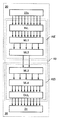
- the NN circuit 40 is a circuit using a neural network, and an example is shown in FIG. In addition to the NN circuit 40, the circuit 22a and the GPU 31 are also illustrated in FIG.
- the encoder AIE included in the NN circuit 40 includes an input layer INL, an intermediate layer ML1, and an intermediate layer ML2.
- the decoder AID included in the NN circuit 40 includes an intermediate layer ML3, an intermediate layer ML4, and an output layer OUL. And having. That is, in the NN circuit 40, a hierarchical neural network is configured by the input layer INL, the intermediate layers ML1 to ML4, and the output layer OUL.
- the image data sent from the circuit 22a is input to the input layer INL of the encoder AIE included in the NN circuit 40. That is, the image data is handled as input data of a hierarchical neural network.
- a hierarchical neural network will be described in a third embodiment.
- the purpose of the hierarchical neural network in the encoder AIE is to compress input data by feature extraction. Therefore, it is preferable that the number of neurons included in the intermediate layer ML2 is smaller than the number of neurons included in the input layer INL.
- the hierarchical neural network in the encoder AIE shown in FIG. 2 has a configuration in which the number of neurons decreases as the hierarchy progresses. That is, the number of neurons included in the intermediate layer ML1 is smaller than the number of neurons included in the input layer INL, and the number of neurons included in the intermediate layer ML2 is smaller than the number of neurons included in the intermediate layer ML1. Yes.
- the number of neurons in the intermediate layer ML1 may be larger or smaller than the number of neurons in the input layer INL or the intermediate layer ML2.
- the purpose of the hierarchical neural network in the decoder AID is to restore the feature-extracted data. Therefore, it is preferable that the output layer OUL has more neurons than the intermediate layer ML3 has.
- the hierarchical neural network in the decoder AID shown in FIG. 2 has a configuration in which the number of neurons increases as the hierarchy progresses. That is, the number of neurons included in the intermediate layer ML4 is larger than the number of neurons included in the intermediate layer ML3, and the number of neurons included in the output layer OUL is larger than the number of neurons included in the intermediate layer ML4. Yes. Note that the number of neurons in the intermediate layer ML4 may be larger or smaller than the number of neurons in the intermediate layer ML3 or the output layer OUL.
- the number of neurons in the intermediate layer ML2 is the smallest in the encoder AIE
- the number of neurons in the intermediate layer ML3 is the smallest in the decoder AID. Therefore, it is possible to reduce the number of wires connecting the neurons of the intermediate layer ML2 and the neurons of the intermediate layer ML3. That is, the number of wirings that electrically connect the decoder AID of the peripheral circuit 30 and the encoder AIE of the imaging device 20 can be reduced.
- an analog signal corresponding to the image data is sent from the imaging unit 21 to the encoder AIE via the circuit 22a, so that the image data is converted into image data obtained by feature extraction. Is called.
- the decoder AID of the NN circuit 40 performs processing for restoring the extracted image data to the original image data and outputting the original image data as an analog signal from the output layer OUL.
- the restored image data output from the output layer OUL of the decoder AID of the NN circuit 40 is transmitted to the GPU 31.
- connection between the layers can be a full connection or a partial connection.
- a hierarchical neural network is configured by the input layer INL, the intermediate layers ML1 to ML4, and the output layer OUL. It is not limited to this.
- the hierarchical neural network may have a configuration in which the number of intermediate layers of the NN circuit 40 shown in FIG. 2 is changed.
- the imaging device 20 shown in FIG. 1 can function as an image sensor chip described in a sixth embodiment to be described later.
- an NN circuit of the electronic device 10 can be configured by the encoder AIE included in the imaging device 20 and the decoder AID included in the peripheral circuit 30.
- the NN circuit 40 can reduce the number of wirings that electrically connect the encoder AIE and the decoder AID, when the imaging device 20 is mounted on an electronic substrate as a chip, the chip And the number of wirings that electrically connect the electronic substrate can be reduced. That is, with the configuration described in this embodiment, high-resolution image data acquired by the imaging unit 21 can be transmitted to the peripheral circuit 30 with a small number of wires.
- the electronic apparatus 10 shown in FIG. 1 has a configuration in which the imaging device 20 has an encoder AIE and the peripheral circuit 30 has a decoder AID, but the input layer, intermediate layer, and output layer that constitute the neural network are shown in FIG. It is not necessary to have the configuration shown in FIG.
- the encoder AIE may be configured by the input layer INL and the intermediate layer ML1
- the decoder AID may be configured by the intermediate layer ML2 and the output layer OUL.
- the encoder AIE may be configured by the input layer INL and the intermediate layer ML3, and in the peripheral circuit 30, the decoder AID may be configured by the intermediate layer ML4 and the output layer OUL.
- the electronic device 10 shown in FIG. 1 has the display device 50, the display device 50 may not be provided depending on the form of the electronic device. The same applies to other components included in the electronic device 10.
- the NN circuit 40 shown in FIG. 2 is described as one neural network, but one embodiment of the present invention is not limited to this.
- the encoder AIE that performs feature extraction and the decoder AID that performs restoration can be described as independent neural networks. That is, the neural networks formed by the encoder AIE and the decoder AID can be called a first neural network and a second neural network.
- CNN is one of the calculation models used when extracting features such as images.
- FIG. 3 shows a configuration example of the CNN.
- the CNN includes a convolution layer CL, a pooling layer PL, and a total coupling layer FCL.
- CNN is used for the encoder AIE, the image data IPD output from the imaging unit 21 is input to the CNN, and feature extraction is performed.
- the convolution layer CL has a function of performing convolution processing on image data.
- the convolution process is performed by repeating a product-sum operation between part of the image data and the filter value of the weight filter.
- Image feature extraction is performed by a convolution process in the convolution layer CL.
- One or a plurality of weight filters can be used for the convolution process.
- a plurality of weight filters are used, a plurality of features included in the image data can be extracted.
- FIG. 3 shows an example in which three filters (filters fill a , fill b , and fill c ) are used as weight filters.
- the image data input to the convolution layer CL is subjected to filter processing using the filters fil a , fil b , and fil c , and data D a , D b , and D c are generated.
- the data D a , D b , and D c subjected to the convolution process are converted by the activation function and then output to the pooling layer PL.
- the activation function ReLU (Rectified Linear Unit) or the like can be used.
- ReLU is a function that outputs “0” when the input value is negative, and outputs the input value as it is when the input value is “0” or more.
- a sigmoid function, a tanh function, etc. can also be used as an activation function.
- the pooling layer PL has a function of performing a pooling process on the image data input from the convolution layer CL.
- the pooling process is a process of dividing image data into a plurality of areas, extracting predetermined data for each area, and arranging the data in a matrix. By performing the pooling process, it is possible to reduce the image data while leaving the features extracted by the convolution layer CL.
- maximum pooling, average pooling, Lp pooling, or the like can be used as the pooling process.
- the CNN performs feature extraction by the above convolution processing and pooling processing.
- the CNN can be composed of a plurality of convolution layers CL and a pooling layer PL.
- a layer L composed of a convolution layer CL and a pooling layer PL is provided (z is an integer equal to or greater than 1) (layers L 1 to L z ), and the convolution process and the pooling process are performed z times.
- the configuration to be performed is shown. In this case, feature extraction can be performed in each layer L, and more advanced feature extraction is possible.
- FIG. 3 the layer L 1 , the layer L 2 , and the layer L z are illustrated, and the other layers L are omitted.
- the fully connected layer FCL has a function of determining an image using image data that has been subjected to convolution processing and pooling processing.
- the fully coupled layer FCL has a configuration in which all nodes in one layer are connected to all nodes in the next layer.
- the image data output from the convolution layer CL or the pooling layer PL is a two-dimensional feature map, and when input to the all coupling layer FCL, it is developed in one dimension. Then, the image data OPD obtained by inference by all the coupling layers FCL is output.
- the configuration of the CNN is not limited to the configuration of FIG.
- the pooling layer PL may be provided for each of the plurality of convolution layers CL. Further, when it is desired to retain the position information of the extracted features as much as possible, the pooling layer PL may be omitted.
- an output layer electrically connected to all the coupling layers FCL may be provided.
- the output layer can output a classification class using a softmax function or the like as a likelihood function.
- the CNN can perform supervised learning using image data as learning data and teacher data.
- supervised learning for example, an error back propagation method can be used.
- the filter value of the weight filter, the weight coefficient of all coupling layers, and the like can be optimized.
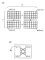
- FIG. 4A shows a plurality of pixels pix of n rows and m columns (here, n and m are integers of 1 or more) arranged in a matrix in the imaging unit 21.
- pixel data corresponding to the imaging target is captured by imaging.
- description will be made assuming that pixel data g [1,1] to pixel data g [n, m] are captured in the pixels pix [1,1] to pix [n, m], respectively.
- FIG. 4B shows a filter file a composed of addresses of t rows and s columns (where t is an integer of 1 to n and s is an integer of 1 to m).
- a filter value f a [1, 1] to a filter value f a [t, s] are assigned to each address of the filter fill a .
- data indicating predetermined features may be stored in the filter values f a [1, 1] to f a [t, s]. it can. Then, at the time of feature extraction, the feature data and the image data are compared.
- filter value f a [1,1] to the filter value f a [s, t] in stores parameters necessary for image processing be able to.
- FIG. 5A illustrates a pixel region P having corners of the pixel pix [1,1], the pixel pix [1, s], the pixel pix [t, 1], and the pixel pix [t, s].
- a state is shown in which data D a [1,1] is acquired by performing filter processing using the filter fill a on [1,1].
- this filter processing is performed by using pixel data of one pixel pix included in the pixel area P [1, 1] and the filter value f a of the filter fill a corresponding to the address of the pixel pix.
- the multiplication results for each pixel pix are added together.
- pixel data g [v, w] (where v is an integer of 1 to t and w is an integer of 1 to s.
- the data D a [1,1] can be expressed by the following equation.
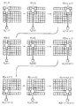
- the above product-sum operation is sequentially performed for other pixel regions. Specifically, as shown in FIG. 6, the pixel pix [1,2], the pixel pix [1, s + 1], the pixel pix [t, 2], and the pixel pix [t, s + 1] Is filtered to obtain data D a [1,2]. Similarly, the pixel area P is moved by one column at a time, and data Da is acquired in each pixel area P.
- a pixel region P [with corners of the pixel pix [1, m ⁇ s + 1], the pixel pix [1, m], the pixel pix [t, m ⁇ s + 1], and the pixel pix [t, m]. 1, m-s + 1] to obtain data D a [1, m-s + 1] from after the acquisition of the data D a of one line is completed, the pixel region P is moved one row pixel, similarly 1 sequentially acquires the data D a of rows.
- Figure 6 is a state pixel region P [2,1] to the pixel region P [2, m-s + 1] from the data D a [2,1] to the data D a [2, m-s + 1] is obtained Show.
- the filtering process using the filter fill a for all the pixel regions P Ends.
- the pixel pix [1, 1] to the pixels pix [n, m] a matrix of pixel regions P of t rows s column is selected, filter using a filter fil a with respect to the pixel region P Processing is performed.
- a pixel pix [x, y] (where x is an integer between 1 and n ⁇ t + 1 and y is an integer between 1 and m ⁇ s + 1), and a pixel pix [x, y + s ⁇ 1].
- Pixel pix [x + t ⁇ 1, y] and pixel pix [x + t ⁇ 1, y + s ⁇ 1] are obtained by performing a filter process using the filter “fil a” on the pixel region P having corners.
- the data D a [x, y] can be expressed by the following formula.
- the filtering process using the filter “fil a” is performed on all the pixel regions P of t rows and s columns that can be selected from the pixels pix [1,1] to pix [n, m].
- data D a [1,1] to data D a [n ⁇ t + 1, m ⁇ s + 1] can be obtained.
- the feature map shown in FIG. 7 is obtained.
- the convolution process is performed by the product-sum operation using the image data and the filter value, and the feature extraction of the image is performed.
- the above convolution process is performed for each filter file.
- the pixel region P is in the first column to the ms column, the pixel region P is moved by one pixel, or when the pixel region P is in the m-s + 1 column, although an example has been described in which P is returned to the first column and the pixel region P is moved by one pixel row, the moving distance of the pixel region P can be freely set.
- ⁇ Circuit 22a> a configuration example of the circuit 22a when the NN circuit 40 described in the first embodiment performs the above-described calculation of the CNN will be described.
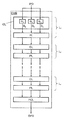
- FIG. 8 shows a configuration example of the circuit 22a. In FIG. 8, not only the circuit 22a but also the encoder AIE is shown.
- the imaging unit 21 of the imaging device 20 includes n rows and m columns of pixels (hereinafter referred to as pixels pix [1, 1] to pix [n, m]) arranged in a matrix.
- the circuit 22a will be described by taking as an example a case where a convolution process is performed on a pixel of n rows and m columns using a filter fill a of t rows and s columns.
- the circuit 22a has a shift register.
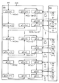
- the shift register includes a t ⁇ m-stage holding circuit HC, an input terminal IPT, t ⁇ s output terminals PT, and a terminal to which a clock signal CLK is input.
- the t ⁇ m-stage holding circuits HC are referred to as holding circuits HC [1] to HC [tm], respectively, and t ⁇ s output terminals PT are output terminals PT [1]. To the output terminal PT [ts].
- the input terminal IPT is electrically connected to the imaging unit 21.
- the image data acquired by the imaging unit 21 is input pixel by pixel to the input terminal IPT of the circuit 22a.
- the holding circuits HC [dm + 1] to the holding circuit HC [dm + s] (where d is an integer from 0 to t ⁇ 1).
- the output terminals PT [ds + 1] to PT [(d + 1) s] are electrically connected. That is, in FIG. 8, the holding circuit HC [1] to the holding circuit HC [s] are electrically connected to the output terminal PT [1] to the output terminal PT [s], respectively, and the holding circuit HC [m + 1] to the holding circuit.
- the circuit HC [m + s] is electrically connected to the output terminal PT [s + 1] to PT [2s], respectively, and the holding circuit HC [(t ⁇ 1) m + 1] to the holding circuit HC [(t ⁇ 1) m + s. ] Are electrically connected to the output terminal PT [(t ⁇ 1) s + 1] to the output terminal PT [ts], respectively.
- the encoder AIE has a wiring RW [1] to a wiring RW [ts].
- the wirings RW [1] to RW [ts] are electrically connected to the output terminals PT [1] to PT [ts], respectively.
- the wiring RW [1] to RW [ts] the wiring RW [1], the wiring RW [2], the wiring RW [s], the wiring RW [s + 1], the wiring RW [s + 2]
- Only the wiring RW [2s], the wiring RW [(t ⁇ 1) s + 1], the wiring RW [(t ⁇ 1) s + 2], and the wiring RW [ts] are denoted by reference numerals.
- the encoder AIE has a memory cell array of ts rows (not shown in FIG. 8). In one column of memory cells included in the memory cell array, filter values f a [1, 1] to f a [t, s] of the filter file a used in the convolution process are held.
- the memory cell array CA described in Embodiment 3 is referred to as a specific configuration of the memory cell array.
- the memory cell array CA is one of the components of the product-sum operation circuit.
- the encoder AIE has a product-sum operation circuit.
- the product-sum operation circuit can execute a product-sum operation on data (filter value, weight coefficient, etc.) held in the memory cell and data (image data, etc.) input to the wiring RW.
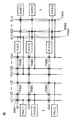
- Pixel data g [1,1] to pixel data g [n, m] captured by the pixels pix [1,1] to pix [n, m] of the imaging unit 21 are input to the input terminal IPT of the circuit 22a. They are entered in order. Each time the clock signal CLK is input, the circuit 22a transmits the pixel data held in the holding circuit HC to the holding circuit HC in the next stage.
- FIG. 8 shows a diagram in which the pixel data g [1,1] is transmitted to the holding circuit HC [1] and the pixel data g [t, m] is transmitted to the holding circuit HC [tm].
- the pixel data held in the holding circuit HC [dm + 1] to the holding circuit HC [dm + s] is output from the output terminal PT [ds + 1] to the output terminal PT [(d + 1) s], respectively. That is, in FIG.
- pixel data g [1,1] to pixel data g [1, s] are output from the output terminal PT [1] to output terminal PT [s], respectively, and the pixel data g [2,1 ] To pixel data g [2, s] are respectively output from the output terminals PT [s + 1] to PT [2s], and the pixel data g [t, 1] to pixel data g [t, s] are respectively The signals are output from the output terminal PT [(t ⁇ 1) s + 1] to the output terminal PT [ts].
- the respective pixel data held in the holding circuit HC [dm + 1] to the holding circuit HC [dm + s] are transmitted to the wiring RW [ds + 1] to the wiring RW [(d + 1) s] of the memory cell array of the encoder AIE.
- all the pixel data transmitted to the wirings RW [1] to RW [ts] correspond to the image data of the pixel region P [1, 1] illustrated in FIGS. .
- the image data of the pixel region P [1,1] output to the wiring RW [1] to the wiring RW [ts] is supplied to one column of memory cells included in the memory cell array in the ts row of the encoder AIE.
- filter values f a [1, 1] to filter values f a [t, s] are held in the memory cells in one column, and a product-sum operation is performed on the image data and the filter value fa. .
- Embodiment 3 for details of the product-sum operation.
- Data D a [1,1] shown in FIG. 5 can be obtained by product-sum operation of the image data of the pixel region P [1,1] and the filter fill a .
- the circuit 22a has a function of collectively outputting t ⁇ s image data to the encoder AIE, so that the convolution process can be performed at high speed.
- the number of columns in the memory cell array of the encoder AIE may be the number of the filters. Details of this will be described in Embodiment 3.
- the pixel data held in the holding circuit HC [dm + 1] to the holding circuit HC [dm + s] is output from the output terminal PT [ds + 1] to the output terminal PT [(d + 1) s], respectively. That is, in FIG.
- the pixel data g [1,2] to pixel data g [1, s + 1] are output from the output terminals PT [1] to PT [s], respectively, and the pixel data g [2,2 ] To pixel data g [2, s + 1] are respectively output from the output terminals PT [s + 1] to PT [2s], and the pixel data g [t, 2] to pixel data g [t, s + 1] are respectively The signals are output from the output terminal PT [(t ⁇ 1) s + 1] to the output terminal PT [ts].
- the respective pixel data held in the holding circuit HC [dm + 1] to the holding circuit HC [dm + s] are transmitted to the wiring RW [ds + 1] to the wiring RW [(d + 1) s] of the memory cell array of the encoder AIE.
- all the pixel data transmitted to the wiring RW [1] to the wiring RW [ts] correspond to the image data of the pixel region P [1,2] illustrated in FIG.
- Data D a [1,2] shown in FIG. 6 can be obtained by the product-sum operation.
- the image data of the pixel region P moved by one column of pixels is converted into the circuit 22a. Can be entered sequentially.
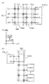
- the circuit 22a shown in FIG. 10 shows a state in which the pulse of the clock signal CLK is inputted from the state shown in FIG. 9 and the pixel data g is sequentially inputted from the input terminal IPT. Yes. That is, in FIG. 10, pixel data g [1, m ⁇ s + 1] to pixel data g [1, m] are output from the output terminal PT [1] to output terminal PT [s], respectively, and the pixel data g [2 , M ⁇ s + 1] to pixel data g [2, m] are output from the output terminal PT [s + 1] to output terminal PT [2s], respectively, and the pixel data g [t, m ⁇ s + 1] to pixel data g [t , M] are output from the output terminal PT [(t ⁇ 1) s + 1] to the output terminal PT [ts], respectively.
- the respective pixel data held in the holding circuit HC [dm + 1] to the holding circuit HC [dm + s] is transmitted to the wiring RW [ds + 1] to the wiring RW [(d + 1) s] of the memory cell array of the encoder AIE.
- all the pixel data transmitted to the wiring RW [1] to the wiring RW [ts] correspond to the image data of the pixel region P [1, m ⁇ s + 1] illustrated in FIG. 6.
- the image data of the pixel area P [1, m ⁇ s + 1] sent through the wiring RW [1] to the wiring RW [ts] is the same as the pixel area P [1, 1] and the pixel area P [1, 2]. , filtering by filter fil a is performed. Specifically, the image data of the pixel region P [1, m ⁇ s + 1] and the filter values f a [1, 1] to f a [t, s] held in a certain column of memory cells.
- the data D a [1, m ⁇ s + 1] shown in FIG. 6 can be obtained by the product-sum operation.
- the pixel data g and the clock signal CLK are sequentially input, and the convolution processing is performed on each image data of the pixel region P [1,1] to the pixel region P [1, m ⁇ s + 1]. it is, it is possible to acquire the data D a of one line.
- the pixel area in which the convolution process is performed next is the pixel area P [2, 1].
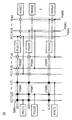
- the image data of the pixel region P [2,1] is stored in the memory of the encoder AIE by inputting the s number of pulses of the clock signal CLK and the pixel data g to the circuit 22a from the state shown in FIG. It can be input to the cell array.
- pixel data g [2,1] to pixel data g [2, s] are output from output terminals PT [1] to PT [s], respectively, and pixel data g [3,1] to Pixel data g [3, s] are output from output terminals PT [s + 1] to PT [2s], respectively, and pixel data g [t + 1, 1] to pixel data g [t + 1, s] are output terminals, respectively. It is output from PT [(t ⁇ 1) s + 1] to the output terminal PT [ts].
- the respective pixel data held in the holding circuit HC [dm + 1] to the holding circuit HC [dm + s] are transmitted to the wiring RW [ds + 1] to the wiring RW [(d + 1) s] of the memory cell array of the encoder AIE.
- all the pixel data transmitted to the wirings RW [1] to RW [ts] correspond to the image data of the pixel region P [2, 1] illustrated in FIG.
- the image data of the pixel region P [2,1] sent through the wiring RW [1] to the wiring RW [ts] is the same as the pixel region P [1,1] to the pixel region P [1, m ⁇ s + 1]. , filtering by filter fil a is performed. Specifically, the image data of the pixel region P [2, 1] and the filter values f a [1, 1] to f a [t, s] held in a certain column of memory cells. Data D a [2, 1] shown in FIG. 6 can be obtained by the product-sum operation.
- the circuit 22a has a function of sequentially transmitting image data to the memory cell array of the encoder AIE for each pixel area. Therefore, the product-sum operation in CNN can be performed at high speed by using the circuit 22a.
- circuit 22a illustrated in FIGS.
- the circuit configuration of the circuit 22a can be changed as appropriate according to the situation.
- ⁇ Hierarchical neural network> As one type of neural network that can be used for the semiconductor device of one embodiment of the present invention, a hierarchical neural network will be described.
- FIG. 12 is a diagram showing an example of a hierarchical neural network.
- the (k ⁇ 1) th layer (where k is an integer of 2 or more) has P neurons (where P is an integer of 1 or more), and the kth layer is a neuron.
- Q (here, Q is an integer of 1 or more)
- the (k + 1) -th layer has R neurons (where R is an integer of 1 or more).
- the product of the output signal z p (k ⁇ 1) and the weighting factor w qp (k) of the p-th neuron in the (k ⁇ 1) -th layer (where p is an integer of 1 or more and P or less) is It is assumed that the input signal is input to the q-th neuron in the k-th layer (where q is an integer of 1 to Q), and the output signal z q (k) of the q-th neuron in the k-th layer and the weight coefficient w rq.
- the output signal z q (k) from the q-th neuron in the k-th layer is defined by the following equation.
- the function f (u q (k) ) is an activation function, and a step function, a linear ramp function, a sigmoid function, or the like can be used.
- the product-sum operation of Expression (D1) can be realized by a multiplication circuit, an addition circuit, or the like.
- the calculation of the expression (D2) can be realized by, for example, the circuit 71 illustrated in FIG.
- the activation function may be the same or different in all neurons. In addition, the activation function may be the same or different for each layer.
- a hierarchical neural network composed of all L layers (L is an integer of 3 or more) shown in FIG. 13 is considered (that is, k here is 2 or more and (L ⁇ 1) or less). An integer.)
- the first layer is an input layer of the hierarchical neural network
- the L layer is an output layer of the hierarchical neural network
- the second to (L-1) layers are hidden by the hierarchical neural network. Become a layer.
- the first layer has P neurons
- the kth layer has Q [k] neurons (Q [k] is an integer equal to or greater than 1).
- the L layer has R neurons.
- the output signal of the s [1] neuron in the first layer (s [1] is an integer between 1 and P) is z s [1] (1), and the s [k] neuron in the kth layer.
- the output signal (s [k] is an integer between 1 and Q [k]) is z s [k] (k), and the s [L] neuron (s [L] is 1 in the Lth layer.
- the output signal is an integer less than or equal to R.) z s [L] (L) .
- the output signal z s [k ⁇ 1 ] of the s [k ⁇ 1] th neuron (s [k ⁇ 1] is an integer of 1 to Q [k ⁇ 1]) in the (k ⁇ 1) th layer.
- Product k s [k] (k ) and weight coefficient w s [k] s [k ⁇ 1] (k) are input to the s [k] neuron in the k-th layer.
- the output signal z s [L ⁇ ] of the s [L ⁇ 1] neuron (s [L ⁇ 1] is an integer of 1 to Q [L ⁇ 1]) in the (L ⁇ 1) th layer.
- 1] (L ⁇ 1) and the weight coefficient w s [L] s [L ⁇ 1] (L) and the product u s [L] (L) are input to the s [L] neuron in the Lth layer.
- Supervised learning means that when the output result and the desired result (sometimes referred to as teacher data or teacher signal) differ in the above-described hierarchical neural network, the hierarchical neural network This is an operation for updating all the weight coefficients based on the output result and the desired result.
- FIG. 14 is a diagram illustrating a learning method using an error back propagation method.
- the error back-propagation method is a method of changing the weighting coefficient so that the error between the output of the hierarchical neural network and the teacher data becomes small.
- the update amount of the weight coefficient w s [k] s [k ⁇ 1] (k) of the s [k] neuron in the k-th layer is expressed as ⁇ E / ⁇ w s [k] s [k ⁇ 1]
- the weighting factor can be newly changed.
- f ′ (u s [k] (k) ) is a derivative of the activation function.
- the calculation of the expression (D3) can be realized by, for example, the circuit 73 illustrated in FIG.
- the calculation of the equation (D4) can be realized by, for example, the circuit 74 shown in FIG.
- the activation function can be realized, for example, by connecting an arithmetic circuit corresponding to a desired derivative to the output terminal of the operational amplifier.
- the calculation of the part of ⁇ s [k + 1] (k + 1) ⁇ w s [k + 1] ⁇ s [k] (k + 1) in the equation (D3) can be realized by an addition circuit and a multiplication circuit.
- ⁇ s [L] (L) and ⁇ E / ⁇ w s [L] s [L -1] (L) can be represented by the following formulas.
- the errors ⁇ s [k] (k) and ⁇ s [L] (L) of all the neuron circuits can be obtained from the equations (D1) to (D6).
- the weight coefficient update amount is set based on the errors ⁇ s [k] (k) , ⁇ s [L] (L), desired parameters, and the like.
- FIG. 16 is a block diagram showing a configuration example of a circuit of a hierarchical neural network.
- An NN (neural network) circuit 80 includes input terminals PDL [1] to PDL [1] (where l is an integer of 1 or more), output terminals PDR [1] to output terminals PDR [n]. (Where n is an integer greater than or equal to 1), programmable logic element PLE [1] to programmable logic element PLE [m], wiring L [1] to wiring L [l], wiring P [1] to wiring P [m], wirings R [1] to R [m], wirings Q [1] to Q [m], a plurality of programmable switches PSW1, a plurality of programmable switches PSW2, and a plurality of programmable switches PSW3.
- the NN circuit 80 is a multi-context programmable operation processing device using the programmable logic element PLE [1] to the programmable logic element PLE [m] and the programmable switch PSW1 to the programmable switch PSW3.
- the arithmetic processing device associates the connection state of the network between each hierarchy with each context, and the neural network arithmetic processing is performed by sequentially switching the context. It can be performed.
- the input terminal PDL [i] (where i is an integer of 1 to 1) is electrically connected to the wiring L [i].
- the output terminal PDR [k] (where k is an integer from 1 to n) is electrically connected to each of the wirings R [1] to R [m] via the programmable switch PSW3.
- a first terminal of the programmable logic element PLE [j] (where j is an integer of 1 to m) is electrically connected to the wiring Q [j]
- the wiring Q [j] [1] to each of the wirings L [l] are electrically connected via the programmable switch PSW1.
- the wiring Q [j] is electrically connected to each of the wirings P [1] to P [m] through the programmable switch PSW2.
- a second terminal of the programmable logic element PLE [j] is electrically connected to the wiring R [j].
- the wirings P [1] to P [m] are electrically connected to the wirings R [1] to R [m], respectively.
- the programmable switches PSW1 to PSW3 included in the NN circuit 80 are switches that can be switched between a conductive state and a non-conductive state according to configuration data stored in a configuration memory CMS described later.
- Each of the programmable switches PSW1 to PSW3 includes a switch circuit SWC. Details of the programmable switches PSW1 to PSW3 will be described later.
- the programmable logic element PLE has an arithmetic processing circuit 90 shown in FIG.
- the arithmetic processing circuit 90 includes an input terminal In [1] to an input terminal In [s] (where s is an integer equal to or greater than 1), an output terminal OUT, and a multiplier circuit MLT [1] to a multiplier circuit MLT. [S], an adder circuit AD, an activation function circuit FC, a holding circuit KC, a configuration memory CMW [1] to a configuration memory CMW [s], and a configuration memory CMF.
- the configuration memory CMW [1] to the configuration memory CMW [s] may be a single configuration memory.
- the configuration memory CMW [1] to the configuration memory CMW [s] and the configuration memory CMF may be a single configuration memory.
- the input terminal In [h] (where h is an integer of 1 to s) is electrically connected to the input terminal of the multiplier circuit MLT [h], and the output terminal of the multiplier circuit MLT [h] is Are electrically connected to the input terminal of the adder circuit AD.
- the output terminal of the adder circuit AD is electrically connected to the input terminal of the activation function circuit FC.
- the output terminal of the activation function circuit FC is electrically connected to the terminal TA1 of the holding circuit KC.
- a terminal TA2 of the holding circuit KC is electrically connected to the output terminal OUT.
- the multiplication circuit MLT [h] uses data (hereinafter referred to as a weighting factor) held in the configuration memory CMW [h] as a multiplier, and an input signal input to the input terminal In [h] as a multiplicand. It is a circuit that performs multiplication.
- the adder circuit AD is a circuit that calculates the sum of the multiplication results output from the multiplication circuits MLT [1] to MLT [s]. That is, the product-sum operation circuit is configured by the multiplier circuits MLT [1] to MLT [s] and the adder circuit AD.
- the activation function circuit FC is a circuit that performs an operation according to a function system defined by data held in the configuration memory CMF with respect to a signal input to the input terminal, that is, a product-sum operation result.
- a function system for example, a sigmoid function, a tanh function, a softmax function, a ReLU function, a threshold function, or the like can be used.
- the holding circuit KC acquires the calculation result output from the activation function circuit FC from the terminal TA1, and has a function of temporarily holding the calculation result, and a function of outputting the temporarily held calculation result to the terminal TA2.
- the holding circuit KC can switch between the two functions described above according to the clock signal CLK input to the terminal CKT.
- the holding circuit KC can hold the potential input from the terminal TA1, and when the clock signal CLK is at a low level potential, the holding circuit KC is set at the terminal TA2. To the output terminal OUT.
- the arithmetic processing circuit 90 is a circuit that handles digital data, for example, a flip-flop circuit can be applied to the holding circuit KC.
- a holding circuit KC shown in FIG. 17B is a sample-and-hold circuit, and includes a transistor TrA, a transistor TrB, a capacitor CP, an amplifier AMP, and a NOT circuit NL.
- the first terminal of the transistor TrA is electrically connected to the terminal TA1
- the second terminal of the transistor TrA is electrically connected to the first terminal of the capacitor CP
- the gate of the transistor TrA is electrically connected to the terminal CKT. It is connected to the.
- the input terminal of the amplifier AMP is electrically connected to the second terminal of the transistor TrA
- the output terminal of the amplifier AMP is electrically connected to the first terminal of the transistor TrB.
- the second terminal of the transistor TrB is electrically connected to the terminal TA2.
- the input terminal of the NOT circuit NL is electrically connected to the terminal CKT
- the output terminal of the NOT circuit NL is electrically connected to the gate of the transistor TrB.
- the second terminal of the capacitor CP is electrically connected to the wiring GNDL. Note that a node N is a connection point of the second terminal of the transistor TrA, the input terminal of the amplifier AMP, and the first terminal of the capacitor CP.
- the amplifier AMP has a function of amplifying the signal input to the input terminal by a factor of 1 and outputting the amplified signal to the output terminal.
- the wiring GNDL is a wiring that applies a reference potential.
- the transistor TrA When the clock signal CLK input to the terminal CKT is at a high level potential, the transistor TrA is turned on and the transistor TrB is turned off. At this time, the signal input from the terminal TA1 is input to the amplifier AMP via the transistor TrA. Therefore, the amplifier AMP amplifies the signal and outputs the amplified signal from the output terminal of the amplifier AMP. Note that since the transistor TrB is non-conductive, the amplified signal is not output from the terminal TA2.
- the potential of the node N is held by the capacitive element CP. At this time, the potential of the node N becomes the potential of the signal input from the terminal TA1.
- the transistor TrA When the clock signal CLK input to the terminal CKT is at a low level potential, the transistor TrA is turned off and the transistor TrB is turned on. Since the transistor TrA is in a non-conductive state, the potential of the node N does not change.
- the amplifier AMP outputs the potential of the node N to the first terminal of the transistor TrB. Since the transistor TrB is in a conductive state, the potential of the node N, that is, the potential of the signal input from the terminal TA1 when the clock signal CLK is at a high level is output from the terminal TA2.
- the transistor TrA and / or the transistor TrB is preferably an OS transistor described in Embodiment 5.
- the OS transistor preferably uses an oxide containing at least one of indium, element M (such as aluminum, gallium, yttrium, and tin) and zinc in the channel formation region.
- FIG. 17A the input terminal In [1], the input terminal In [2], the input terminal In [s], the multiplier circuit MLT [1], the multiplier circuit MLT [2], and the multiplier circuit MLT [s].
- the holding circuit KC of the arithmetic processing circuit 90 is not limited to the above-described configuration.
- the configuration of the holding circuit KC can be changed as appropriate depending on the situation.
- the configuration memory CMW [1] to configuration memory CMW [s] and the configuration memory CMF included in the arithmetic processing circuit 90, and a configuration memory CMS for setting states of programmable switches PSW1 to PSW3 described later May be configured to write data by different drive circuits. That is, without updating the data of the configuration memory CMS of the programmable switches PSW1 to PSW3, the data of the configuration memory CMW [1] to the configuration memory CMW [s] and the data of the configuration memory CMF of the arithmetic processing circuit 90 is updated. Updates can be repeated. This enables efficient learning in the neural network.
- each layer can be reduced with less circuit resources by switching the context. Can be sequentially executed.
- one programmable logic element has a single arithmetic processing circuit 90
- one product-sum arithmetic circuit is configured by a plurality of programmable logic elements and a programmable switch that connects the programmable logic elements. It is also possible to configure.
- FIG. 18A illustrates the wiring L [1] to the wiring L [l], the wiring P [1] to the wiring P [m], the wiring Q [j], the programmable switch PSW1, A connection example between the programmable switch PSW2 and the programmable logic element PLE [j] is shown, and FIG. 18B shows a configuration example of the switch circuit SWC.
- the wiring Q [j] includes the wirings q [1] to q [s].
- the first terminals of the programmable logic element PLE [j] are terminals In [1] to In [s] of the arithmetic processing circuit 90 described with reference to FIG. That is, in FIG. 18A, the wiring q [h] is electrically connected to the terminal In [h].
- the wirings q [1] to q [s] are electrically connected to the wiring “0” through the programmable switch PSW1.
- the wiring “0” is a wiring for supplying a signal having a value of 0 (the signal potential is a reference potential).
- the programmable switch PSW1 and the programmable switch PSW2 have a switch circuit SWC.
- a configuration example of the switch circuit SWC is shown in FIG.
- the first terminal of the switch SW is electrically connected to the wiring q [h]
- the second terminal of the switch SW is electrically connected to the wiring X.
- the wiring X is any one of the wiring “0”, the wirings L [1] to L [l], and the wirings P [1] to P [m].
- the switch SW determines a conductive state or a non-conductive state according to data held in the configuration memory CMS.
- each of the programmable switch PSW1 and the programmable switch PSW2 illustrated in FIG. 18A is in a conductive state or a non-conductive state depending on the data in the configuration memory CMS. That is, according to the data in the configuration memory CMS, the wiring “0”, the wirings L [1] to L [l], the wirings P [1] to P [m], and the terminals In [1] to In It is possible to control whether or not each [s] is connected.
- the switch circuit SWC that connects the part of the terminals and the wiring “0” is turned on.
- the multiplier circuits corresponding to the some terminals can reduce power consumption by power gating.
- a switch using a MEMS (micro electro mechanical system) technology such as a transistor, a diode, or a digital micromirror device (DMD) may be applied. it can.
- the switch SW may be a logic circuit that combines transistors. In the case where the switch SW is a single transistor, it is preferable to use an OS transistor having characteristics of extremely low off-state current.
- FIG. 18C illustrates a connection example of the wiring R [k], the programmable switch PSW3, the programmable logic element PLE [j], and the output terminals PDR [1] to PDR [n] in the NN circuit 80. Show.
- the wiring R [k] includes the wirings r [1] to r [t] (here, t is an integer of 1 or more).
- the second terminals of the programmable logic element PLE [j] are illustrated as terminals O [1] to O [t]. That is, the wiring r [u] is electrically connected to the terminal O [u] (where u is an integer of 1 to t).
- a plurality of second terminals are illustrated, but a single terminal may be used. Accordingly, the wirings r [1] to r [t] can be made one wiring.
- the programmable switch PSW3 includes a switch circuit SWC. That is, similarly to the programmable switch PSW1 and the programmable switch PSW2, the conduction state and the non-conduction state of the switch SW included in the switch circuit SWC can be determined by the data held in the configuration memory CMS. For this reason, the presence / absence of connection between each of the terminals O [1] to O [t] and each of the output terminals PDR [1] to PDR [n] is controlled by data in the configuration memory CMS. be able to.
- the configuration memory CMW [1] to the configuration memory CMW [s], and the configuration memory CMF described above for example, SRAM, MRAM, or the like can be applied.
- a memory device using an OS transistor referred to as an OS memory in this specification
- an OS memory for example, a memory device using an OS transistor (referred to as an OS memory in this specification)
- an OS memory for example, a memory device using an OS transistor (referred to as an OS memory in this specification) can be used.
- an OS memory as the configuration memory described above, a low power consumption neural network can be configured with a small number of elements.
- the multiplication circuit MLT [1] By using the multiplication circuit MLT [1] to the multiplication circuit MLT [s] and the addition circuit AD described above as analog product-sum operation circuits, the number of transistors constituting the product-sum operation circuit can be reduced.
- the analog product-sum operation circuit will be described later in this embodiment.
- the NN circuit 80 sets the number of contexts to N. That is, the plurality of configuration memories CMS, the configuration memories CMW [1] to CMW [s], and the configuration memory CMF included in the NN circuit 80 each have N sets of configuration data.
- the neural network handled in this operation example is a hierarchical neural network including an input layer, a first intermediate layer, and an N-1 intermediate layer.
- the (N-1) -th intermediate layer is an output layer in a hierarchical neural network.
- the switch circuit SWC that is in a conductive state is illustrated by a black circle, and the switch circuit SWC that is in a non-conductive state is illustrated by a white circle.
- FIGS. 18A, 18B, and 18C The structures of the wirings Q [1] to Q [m], the wirings R [1] to R [m], and the programmable switches PSW1 to PSW3 are shown in FIGS. 18A, 18B, and 18C. Consider each explanation.
- Context 1 is a configuration corresponding to the network between the input layer and the first intermediate layer.
- the NN circuit 80 in the context 1 is shown in FIG.
- Configuration data is set in the switch PSW3.
- the programmable logic element PLE is set such that the weighting factor of each neuron of the first intermediate layer with respect to the output signal of the neuron of the input layer is set.
- Configuration data is set in [1] to programmable logic element PLE [m].
- a signal input from the input layer to the first intermediate layer corresponds to a signal input from the input terminal PDL [1] to the input terminal PDL [l].
- a signal input from the input terminal PDL [i] is transmitted to each of the wirings Q [1] to Q [m] through the wiring L [i]. Then, the signal sent to the wiring Q [j] is input to the first terminal of the programmable logic element PLE [j].
- a plurality of signals input to the first terminals of the programmable logic elements PLE [1] to PLE [m] are subjected to arithmetic processing by a product-sum arithmetic circuit and an activation function circuit included in each programmable logic element. . Specifically, a product-sum operation of a plurality of signals and a weight coefficient corresponding to each signal and an activation function operation using the product-sum operation result as input information are performed. Note that the weighting factor and the activation function are based on the configuration of the context 1 as described above.
- the output result of the activation function calculation is held by the holding circuit KC shown in FIG. Note that data holding in the holding circuit KC is performed when the potential of the clock signal CLK changes from a low level potential to a high level potential. The data held in the holding circuit KC is output when the potential of the clock signal CLK changes from a high level potential to a low level potential.
- context 2 is selected.
- the context 2 is a configuration corresponding to the network between the first intermediate layer and the second intermediate layer.
- the NN circuit 80 in the context 2 is shown in FIG.
- Configuration data is set in the switch PSW3.
- the programmable logic is set such that the weight coefficient of each neuron of the second intermediate layer is set with respect to the output signal of the neuron of the first intermediate layer.
- Configuration data is set in the elements PLE [1] to programmable logic element PLE [m].
- the data output from the second terminals of the programmable logic element PLE [1] to the programmable logic element PLE [m] is the data stored in the holding circuit KC described above, that is, in the context 1 This is the result of the activation function calculation.
- the result is output from the second terminal of the programmable logic element PLE [1] to the programmable logic element PLE [m] when the clock signal CLK is changed from the high level potential to the low level potential in the holding circuit KC.
- the result output from the second terminal of the programmable logic element PLE [j] is transmitted to each of the wirings Q [1] to Q [m] via the wiring P [j]. Then, the signal sent to the wiring Q [j] is input to the first terminal of the programmable logic element PLE [j].
- a signal input from the first intermediate layer to the second intermediate layer corresponds to a signal output from the second terminal of the programmable logic element PLE [1] to the programmable logic element PLE [m].
- a plurality of signals input to the first terminals of the programmable logic elements PLE [1] to PLE [m] are subjected to arithmetic processing by a product-sum arithmetic circuit and an activation function circuit included in each programmable logic element. . Specifically, a product-sum operation of a plurality of signals and a weight coefficient corresponding to each signal and an activation function operation using the product-sum operation result as input information are performed. Note that the weighting factor and the activation function are based on the configuration of the context 2 as described above.
- the output result of the activation function calculation is held by the holding circuit KC shown in FIG.
- Subsequent operations of the NN circuit 80 are performed in the same manner as the context 2. For example, consider a case where context g (here, g is an integer of 3 to N-1) is selected.
- the context g has a configuration corresponding to the network between the (g-1) -th intermediate layer and the g-th intermediate layer. Note that the contents of FIG. 20 are referred to for the connection state of the NN circuit 80 in the context g.
- Configuration data is set in the switch PSW3. Further, in each of the programmable logic element PLE [1] to the programmable logic element PLE [m], the weighting coefficient of each neuron of the g-th intermediate layer with respect to the output signal of the neuron of the g-1 intermediate layer is set. Configuration data is set in the programmable logic element PLE [1] to the programmable logic element PLE [m].
- the data output from the second terminals of the programmable logic elements PLE [1] to PLE [m] is the data stored in the holding circuit KC described above, that is, the context g ⁇ . 1 is the result of the activation function calculation.
- the result is output from the second terminal of the programmable logic element PLE [1] to the programmable logic element PLE [m] when the clock signal CLK is changed from the high level potential to the low level potential in the holding circuit KC.
- the result output from the second terminal of the programmable logic element PLE [j] is transmitted to each of the wirings Q [1] to Q [m] via the wiring P [j]. Then, the signal sent to the wiring Q [j] is input to the first terminal of the programmable logic element PLE [j].
- a signal input from the (g-1) -th intermediate layer to the g-th intermediate layer corresponds to a signal output from the second terminal of the programmable logic element PLE [1] to the programmable logic element PLE [m].
- a plurality of signals input to the first terminals of the programmable logic elements PLE [1] to PLE [m] are subjected to arithmetic processing by a product-sum arithmetic circuit and an activation function circuit included in each programmable logic element. . Specifically, a product-sum operation of a plurality of signals and a weight coefficient corresponding to each signal and an activation function operation using the product-sum operation result as input information are performed. Note that the weighting factor and the activation function are based on the configuration of the context g as described above.
- the output result of the activation function calculation is held by the holding circuit KC shown in FIG.
- context N is selected.
- the context N is a configuration corresponding to a connection between the (N ⁇ 1) -th intermediate layer (output layer) and the output terminal PDR [1] to the output terminal PDR [n].
- the NN circuit 80 in the context N is shown in FIG.
- Configuration data is set in the switch PSW3.
- the data output from the second terminals of the programmable logic element PLE [1] to the programmable logic element PLE [m] is the data stored in the holding circuit KC described above, that is, the context N ⁇ . 1 is the result of the activation function calculation.
- the result is output from the second terminal of the programmable logic element PLE [1] to the programmable logic element PLE [m] when the clock signal CLK is changed from the high level potential to the low level potential in the holding circuit KC.
- the results output from the second terminals of the programmable logic element PLE [1] to programmable logic element PLE [m] are output to the output terminal PDR [via the wirings R [1] to R [m], respectively. 1] to output terminal PDR [n].
- the output terminal PDR [n] is the output terminal PDR [m].
- the output result of the hierarchical neural network output from the (N-1) -th intermediate layer (output layer) is a signal output from the second terminal of the programmable logic element PLE [1] to programmable logic element PLE [m]. It corresponds to.
- the first intermediate layer to the (N-1) th intermediate layer programmable logic elements that are not used as the neurons of each layer can reduce power consumption by performing the power gating described above. it can.
- the weighting coefficient can be updated by learning.
- a configuration in which configuration data corresponding to each context having a desired neural network configuration is generated, and only the configuration data of the weighting factor of the corresponding context is repeatedly changed is effective.
- the weighting factor can be updated by mounting a dedicated circuit for executing the corresponding arithmetic processing.
- a configuration in which a corresponding arithmetic process is executed by the server is possible.
- the examination and learning of the hierarchical configuration of the neural network is performed by a server, and configuration data for each context corresponding to the optimized hierarchical structure and weighting coefficient obtained by learning is generated, and the configuration data is generated.
- a configuration is possible in which a neural network that performs inference (recognition) is transmitted to the arithmetic processing circuit 90 of the electronic device other than the server, and the arithmetic processing circuit 90 of FIG. 17 is switched to each context in the electronic device. is there.
- the NN circuit 80 By configuring the NN circuit 80 described above, it is possible to realize an arithmetic processing circuit of a neural network that can be used for learning and inference. Further, it is possible to provide a multi-context programmable neural network in which the circuit area is reduced by reducing the number of elements and the number of wirings.
- the NN circuit 80 shown in FIG. 22 shows a configuration example in which the NN circuit 80A is applied as the NN circuit 80 to the encoder AIE, and the NN circuit 80B is applied as the NN circuit 80 to the decoder AID.
- the NN circuit 80A and the NN circuit 80B are electrically connected.
- a circuit 22a and a GPU 31 are also illustrated.
- the NN circuit 40 is configured so that the number of wires for electrically connecting the intermediate layer ML2 of the encoder AIE and the intermediate layer ML3 of the decoder AID is reduced. That is, the encoder AIE may be configured to reduce the number of neurons included in the intermediate layer ML2, and the decoder AID may be configured to decrease the number of neurons included in the intermediate layer ML3.
- the NN circuit 80A includes an input terminal PDL [1] to an input terminal PDL [L] (where L is an integer of 1 or more), an output terminal PDR [1] to an output terminal PDR [N] ( NN circuit 80B includes an input terminal PDL [1] to input terminal PDL [N] and an output terminal PDR [1] to output terminal. PDR [L].
- the plurality of programmable logic elements PLE included in each of the NN circuit 80A and the NN circuit 80B are described as a programmable logic element unit PLES1 and a programmable logic element unit PLES2.
- the NN circuit 40 can be configured by applying the NN circuit 80 to each of the encoder AIE and the decoder AID. Thereby, the image data sent from the circuit 22a can be converted into the image data from which the feature has been extracted by the NN circuit 80A. In addition, the feature-extracted image data can be restored to the original image data by the NN circuit 80B, and the restored image data can be sent to the GPU 31.
- the numbers of the input terminals PDL of the NN circuit 80A and the output terminals PDR of the NN circuit 80B are described as being the same, but depending on the situation, the input terminals PDL of the NN circuit 80A The number of output terminals PDR of the NN circuit 80B may be different from each other.
- FIG. 23 shows a configuration example of the product-sum operation circuit MAC.
- the product-sum operation circuit MAC shown in FIG. 23 is a circuit that performs a product-sum operation on first data held in a memory cell, which will be described later, and input second data.
- the first data and the second data can be analog data or multi-value data (discrete data).
- the product-sum operation circuit MAC includes a current source circuit CS, a current mirror circuit CM, a circuit WDD, a circuit WLD, a circuit CLD, an offset circuit OFST, an activation function circuit ACTV, and a memory cell array CA.
- the memory cell array CA includes a memory cell AM [1], a memory cell AM [2], a memory cell AMref [1], and a memory cell AMref [2].
- the memory cell AM [1] and the memory cell AM [2] have a role of holding the first data, and the memory cell AMref [1] and the memory cell AMref [2] are for performing a product-sum operation. It has a function to hold necessary reference data.
- the reference data can also be analog data or multi-valued data (discrete data), like the first data and the second data.
- the memory cell array CA of FIG. 23 has two memory cells in the row direction and two in the column direction, which are arranged in a matrix. However, the memory cell array CA has three or more memory cells in the row direction. It is good also as a structure arrange
- the memory cell AM [1], the memory cell AM [2], the memory cell AMref [1], and the memory cell AMref [2] each include a transistor Tr11, a transistor Tr12, and a capacitor C1. .
- the transistor Tr11 is preferably an OS transistor.
- the channel formation region of the transistor Tr11 is more preferably an oxide containing at least one of indium, element M (the element M includes aluminum, gallium, yttrium, tin, and the like) and zinc.
- the transistor Tr11 particularly preferably has the structure of the transistor described in Embodiment 5.
- an OS transistor is used as the transistor Tr11, leakage current of the transistor Tr11 can be suppressed, so that a product-sum operation circuit with high calculation accuracy may be realized.
- leakage current from the holding node to the write word line can be extremely reduced when the transistor Tr11 is in a non-conductive state. That is, since the refresh operation of the potential of the holding node can be reduced, the power consumption of the product-sum operation circuit can be reduced.
- the transistor Tr12 can be manufactured simultaneously with the transistor Tr11 by using the OS transistor, the manufacturing process of the product-sum operation circuit may be shortened. Further, the channel formation region of the transistor Tr12 may be made of amorphous silicon, polycrystalline silicon, or the like instead of oxide.
- the first terminal of the transistor Tr11 is electrically connected to the gate of the transistor Tr12. Connected. A first terminal of the transistor Tr12 is electrically connected to the wiring VR. The first terminal of the capacitor C1 is electrically connected to the gate of the transistor Tr12.
- the second terminal of the transistor Tr11 is electrically connected to the wiring WD, and the gate of the transistor Tr11 is electrically connected to the wiring WL [1].
- a second terminal of the transistor Tr12 is electrically connected to the wiring BL, and a second terminal of the capacitor C1 is electrically connected to the wiring CL [1].
- a connection point between the first terminal of the transistor Tr11, the gate of the transistor Tr12, and the first terminal of the capacitor C1 is a node NM [1].
- the second terminal of the transistor Tr11 is electrically connected to the wiring WD, and the gate of the transistor Tr11 is electrically connected to the wiring WL [2].
- a second terminal of the transistor Tr12 is electrically connected to the wiring BL, and a second terminal of the capacitor C1 is electrically connected to the wiring CL [2].
- a connection point between the first terminal of the transistor Tr11, the gate of the transistor Tr12, and the first terminal of the capacitor C1 is a node NM [2].
- a current flowing from the wiring BL to the second terminal of the transistor Tr12 is denoted as IAM [2] .
- the second terminal of the transistor Tr11 is electrically connected to the wiring WDref, and the gate of the transistor Tr11 is electrically connected to the wiring WL [1].
- a second terminal of the transistor Tr12 is electrically connected to the wiring BLref, and a second terminal of the capacitor C1 is electrically connected to the wiring CL [1].
- a connection point between the first terminal of the transistor Tr11, the gate of the transistor Tr12, and the first terminal of the capacitor C1 is a node NMref [1].
- I AMref [1] a current flowing from the wiring BLref to the second terminal of the transistor Tr12 is denoted as I AMref [1] .
- the second terminal of the transistor Tr11 is electrically connected to the wiring WDref, and the gate of the transistor Tr11 is electrically connected to the wiring WL [2].
- a second terminal of the transistor Tr12 is electrically connected to the wiring BLref, and a second terminal of the capacitor C1 is electrically connected to the wiring CL [2].
- the connection point between the first terminal of the transistor Tr11, the gate of the transistor Tr12, and the first terminal of the capacitor C1 is a node NMref [2].
- I AMref [2] a current flowing from the wiring BLref to the second terminal of the transistor Tr12 is denoted as I AMref [2] .
- the node NM [1], the node NM [2], the node NMref [1], and the node NMref [2] described above function as holding nodes for the respective memory cells.
- the wiring VR allows a current to flow between the first terminal and the second terminal of each of the transistors Tr12 of the memory cell AM [1], the memory cell AM [2], the memory cell AMref [1], and the memory cell AMref [2]. Wiring. Therefore, the wiring VR functions as a wiring for applying a predetermined potential. Note that in this embodiment, the potential supplied by the wiring VR can be a reference potential or a potential lower than the reference potential.
- the current source circuit CS is electrically connected to the wiring BL and the wiring BLref.
- the current source circuit CS has a function of supplying current to the wiring BL and the wiring BLref. Note that the amount of current supplied to each of the wiring BL and the wiring BLref may be different from each other. In this configuration example, the current flowing from the current source circuit CS to the wiring BL is I C , and the current flowing from the current source circuit CS to the wiring BLref is I Cref .
- the current mirror circuit CM includes a wiring IL and a wiring ILref.
- the wiring IL is electrically connected to the wiring BL.
- a connection portion between the wiring IL and the wiring BL is illustrated as a node NP.
- the wiring ILref is electrically connected to the wiring BLref.
- a connection point between the wiring ILref and the wiring BLref is a node NPref.
- the current mirror circuit CM has a function of discharging a current corresponding to the potential of the node NPref from the node NPref of the wiring BLref to the wiring ILref and discharging the same amount of the current from the node NP of the wiring BL to the wiring IL.
- the current discharged from the node NP to the wiring IL and the current discharged from the node NPref to the wiring ILref are denoted as I CM .
- the circuit WDD is electrically connected to the wiring WD and the wiring WDref.
- the circuit WDD has a function of transmitting data to be stored in each memory cell included in the memory cell array CA.
- the circuit WLD is electrically connected to the wiring WL [1] and the wiring WL [2].
- the circuit WLD has a function of selecting a memory cell to which data is written when data is written to a memory cell included in the memory cell array CA.
- the circuit CLD is electrically connected to the wiring CL [1] and the wiring CL [2].
- the circuit CLD has a function of applying a potential to the second terminal of the capacitor C1 of each memory cell included in the memory cell array CA.
- the circuit OFST is electrically connected to the wiring BL and the wiring OL.
- the circuit OFST has a function of measuring the amount of current flowing from the wiring BL to the circuit OFST and / or the amount of change in current flowing from the wiring BL to the circuit OFST.
- the circuit OFST has a function of outputting the measurement result to the wiring OL.
- the circuit OFST may have a configuration in which the measurement result is directly output as a current to the wiring OL, or may be converted into a voltage and output to the wiring OL. Note that in FIG. 23, the current flowing from the wiring BL to the circuit OFST is denoted as I ⁇ .
- the circuit OFST can be configured as shown in FIG. In FIG. 24, the circuit OFST includes a transistor Tr21, a transistor Tr22, a transistor Tr23, a capacitor element C2, and a resistor element R1.
- the first terminal of the capacitive element C2 is electrically connected to the wiring BL, and the first terminal of the resistance element R1 is electrically connected to the wiring BL.
- the second terminal of the capacitor C2 is electrically connected to the first terminal of the transistor Tr21, and the first terminal of the transistor Tr21 is electrically connected to the gate of the transistor Tr22.
- the first terminal of the transistor Tr22 is electrically connected to the first terminal of the transistor Tr23, and the first terminal of the transistor Tr23 is electrically connected to the wiring OL.
- an electrical connection point between the first terminal of the capacitor C2 and the first terminal of the resistor R1 is a node Na, the second terminal of the capacitor C2, the first terminal of the transistor Tr21, and the transistor Tr22.
- An electrical connection point with the gate is a node Nb.
- the second terminal of the resistance element R1 is electrically connected to the wiring VrefL.
- the second terminal of the transistor Tr21 is electrically connected to the wiring VaL, and the gate of the transistor Tr21 is electrically connected to the wiring RST.
- a second terminal of the transistor Tr22 is electrically connected to the wiring VDDL.
- a second terminal of the transistor Tr23 is electrically connected to the wiring VSSL, and a gate of the transistor Tr23 is electrically connected to the wiring VbL.
- the wiring VrefL is a wiring that applies a potential Vref
- the wiring VaL is a wiring that applies a potential Va
- the wiring VbL is a wiring that applies a potential Vb.
- the wiring VDDL is a wiring that applies the potential VDD
- the wiring VSSL is a wiring that supplies the potential VSS.
- the potential VDD is a high level potential
- the potential VSS is a low level potential.
- the wiring RST is a wiring that applies a potential for switching between the conductive state and the non-conductive state of the transistor Tr21.
- a source follower circuit is configured by the transistor Tr22, the transistor Tr23, the wiring VDDL, the wiring VSSL, and the wiring VbL.
- a first current (hereinafter referred to as a first current) flows from the wiring BL, the resistance element R1 and the wiring VrefL cause the node Na to respond to the first current and the resistance of the resistance element R1.
- a potential is applied.
- the transistor Tr21 is turned on to apply the potential Va to the node Nb. Thereafter, the transistor Tr21 is turned off.
- a second current (hereinafter referred to as a second current) flows from the wiring BL, similarly to when the first current flows, the resistance element R1 and the wiring VrefL cause the node Na to flow.
- a potential corresponding to the second current and the resistance of the resistance element R1 is applied.
- the potential of the node Nb since the node Nb is in a floating state, the potential of the node Nb also changes due to capacitive coupling when the potential of the node Na changes.
- the change in the potential of the node Na is ⁇ V Na and the capacitive coupling coefficient is 1, the potential of the node Nb is Va + ⁇ V Na .
- the potential Va + ⁇ V Na -V th is output from the wiring OL.
- the potential ⁇ V Na can be output from the wiring OL.
- the potential ⁇ V Na is determined according to the amount of change from the first current to the second current, the resistance element R1, and the potential Vref. Since the resistance element R1 and the potential Vref can be known, the amount of change in the current flowing through the wiring BL can be obtained from the potential ⁇ V Na by using the circuit OFST illustrated in FIG.
- the activation function circuit ACTV is electrically connected to the wiring OL and the wiring NIL.
- the activation function circuit ACTV receives the result of the amount of change in current measured by the circuit OFST via the wiring OL.
- the activation function circuit ACTV is a circuit that performs an operation on the result according to a predefined function system.
- a sigmoid function, a tanh function, a softmax function, a ReLU function, a threshold function, and the like can be used, and these functions are applied as activation functions in the neural network.
- the activation function circuit ACTV can be the activation function circuit FC described above.
- FIG. 25 shows a timing chart of an operation example of the product-sum operation circuit MAC.
- the timing chart in FIG. 25 illustrates the wiring WL [1], the wiring WL [2], the wiring WD, the wiring WDref, the node NM [1], the node NM [2], the node NMref [1], from time T01 to time T09.
- the fluctuation of the potential of the node NMref [2], the wiring CL [1], and the wiring CL [2] is shown, and the fluctuation of the current I B ⁇ I ⁇ and the current I Bref is shown.
- the current I B -I ⁇ indicates the sum of currents flowing from the wiring BL to the memory cells AM [1] and AM [2] of the memory cell array CA.
- ⁇ From time T01 to time T02 a high level potential (indicated as High in FIG. 25) is applied to the wiring WL [1], and a low level potential (Low in FIG. 25) is applied to the wiring WL [2]. Is applied).
- a potential V PR ⁇ V W [1] larger than the ground potential is applied to the wiring WD, and a potential V PR larger than the ground potential is applied to the wiring WDref.
- a reference potential (represented as REFP in FIG. 25) is applied to each of the wiring CL [1] and the wiring CL [2].
- the potential V W [1] is a potential corresponding to one of the first data.
- the potential VPR is a potential corresponding to the reference data.
- V th is the threshold voltage of the transistor Tr12.
- the low-level potential is continuously applied to the wiring WL [2] from before time T02. For this reason, the transistors Tr11 of the memory cell AM [2] and the memory cell AMref [2] are continuously in a non-conductive state from before the time T02.
- the transistors Tr11 of the memory cell AM [1], the memory cell AM [2], the memory cell AMref [1], and the memory cell AMref [2] are in the non-conductive state, from time T02 Until the time T03, the potentials of the node NM [1], the node NM [2], the node NMref [1], and the node NMref [2] are held.
- the OS transistor By applying the OS transistor to the transistor Tr11, the leakage current flowing between the first terminal and the second terminal of the transistor Tr11 can be reduced. Therefore, the node NM [1], the node NM [2], the node NMref [1], In addition, each potential of the node NMref [2] can be held for a long time.
- the ground potential is applied to the wiring WD and the wiring WDref. Since the transistors Tr11 of the memory cell AM [1], the memory cell AM [2], the memory cell AMref [1], and the memory cell AMref [2] are nonconductive, the wiring WD and the wiring WDref The potential held at each of the node NM [1], the node NM [2], the node NMref [1], and the node NMref [2] is not rewritten.
- V W [2] is a potential corresponding to one of the first data.
- the memory cells AM [2] and AMref [2] since a high level potential is applied to the gates of the transistors Tr11 of the memory cells AM [2] and AMref [2], the memory cells AM [2] and AMref [2] The transistor Tr11 becomes conductive. Therefore, in the memory cell AM [2], since the wiring WD and the node NM [2] are electrically connected, the potential of the node NM [2] is V PR ⁇ V W [2] . Similarly, in the memory cell AMREF [2], since the wiring WDref the node Nmref [2] and is electrically connected, the potential of the node Nmref [2], becomes V PR.
- a current from the current source circuit CS is supplied to the wiring BLref.
- current is discharged to the wiring BLref by the current mirror circuit CM, the memory cell AMref [1], and the memory cell AMref [2].
- the following equation is established according to Kirchhoff's law.
- a current from the current source circuit CS is supplied to the wiring BL.
- current is discharged to the wiring BL by the current mirror circuit CM, the memory cell AM [1], and the memory cell AM [2].
- a current flows from the wiring BL to the circuit OFST.
- the following equation is established according to Kirchhoff's law.
- V X [1] is a potential corresponding to one of the second data.
- an increase in the gate potential of the transistor Tr12 is a potential obtained by multiplying the potential change of the wiring CL [1] by a capacitive coupling coefficient determined by the configuration of the memory cell.
- the capacitive coupling coefficient is calculated from the capacitance of the capacitive element C1, the gate capacitance of the transistor Tr12, the parasitic capacitance, and the like.
- the increase in the potential of the wiring CL [1] and the increase in the potential of the gate of the transistor Tr12 are described as the same value. This corresponds to setting the capacitance coupling coefficient of the memory cell AM [1] and the memory cell AMref [1] to 1.
- the potential V X [1] is applied to the second terminal of each of the capacitive elements C1 of the memory cell AM [1] and the memory cell AMref [1], whereby the node NM [1] and the potential of the node NMref [1] rise by V X [1] , respectively.
- IAMref [1] when the current flowing from the wiring BLref to the first terminal via the second terminal of the transistor Tr12 of the memory cell AMref [1] is IAMref [1], 1 , IAMref [1], 1 is It can be expressed by a formula.
- a current I Cref from the current source circuit CS is supplied to the wiring BLref as in the period from time T04 to time T05.
- current is discharged to the wiring BLref by the current mirror circuit CM, the memory cell AMref [1], and the memory cell AMref [2].
- the current discharged by the current mirror circuit CM is I CM, 1 , the following equation is established according to Kirchhoff's law.
- the wiring BL similar to the period from time T04 to time T05, the current I C from the current source circuit CS are supplied. At the same time, current is discharged to the wiring BL by the current mirror circuit CM, the memory cell AM [1], and the memory cell AM [2]. Further, a current flows from the wiring BL to the circuit OFST.
- the wiring BL when the current flowing from the wiring BL to the circuit OFST is I ⁇ , 1 , the following equation is established according to Kirchhoff's law.
- ⁇ I ⁇ is referred to as a differential current in the product-sum operation circuit MAC.
- the differential current ⁇ I ⁇ can be expressed as in the following equation using equations (E1) to (E10).
- each node of the memory cell AM [1] and the memory cell AMref [1] refers to the operation from time T05 to time T06.
- the memory cell AM [2] and the memory cell AMref [2] will be described assuming that the capacity coupling coefficient of each memory cell is 1.
- the potential V X [2] is applied to the second terminal of each of the capacitor C1 of the memory cell AM [2] and the memory cell AMref [2], whereby the node NM [2] and the potential of the node NMref [2] rise by V X [2] , respectively.
- a current I Cref from the current source circuit CS is supplied to the wiring BLref as in the period from time T04 to time T05.
- current is discharged to the wiring BLref by the current mirror circuit CM, the memory cell AMref [1], and the memory cell AMref [2].
- the current discharged by the current mirror circuit CM is I CM, 2 , the following equation is established according to Kirchhoff's law.
- the wiring BL similar to the period from time T04 to time T05, the current I C from the current source circuit CS are supplied. At the same time, current is discharged to the wiring BL by the current mirror circuit CM, the memory cell AM [1], and the memory cell AM [2]. Further, a current flows from the wiring BL to the circuit OFST.
- the wiring BL when the current flowing from the wiring BL to the circuit OFST is I ⁇ , 3 , the following expression is established according to Kirchhoff's law.
- the differential current ⁇ I ⁇ can be expressed as the following equation using the equations (E1) to (E8) and (E12) to (E15).
- the differential current ⁇ I ⁇ input to the circuit OFST corresponds to the sum of the products of the plurality of first data potentials V W and the plurality of second data potentials V X. Value. That is, the sum of products of the first data and the second data can be obtained by measuring the differential current ⁇ I ⁇ with the circuit OFST.
- each V X [1] and V X [2] are applied, but the potential applied to the wiring CL [1] and the wiring CL [2] may be lower than the reference potential REFP.
- REFP a potential lower than the reference potential REFP is applied to the wiring CL [1] and / or the wiring CL [2]
- the memory cell connected to the wiring CL [1] and / or the wiring CL [2] The potential of the holding node can be lowered by capacitive coupling.
- the product of the first data and one of the second data having a negative value can be performed.
- the wiring CL [2] the case of applying -V X [2] rather than V X [2]
- the differential current [Delta] I alpha expressed as the following formula be able to.
- the memory cell array CA having the memory cells arranged in a matrix of 2 rows and 2 columns has been dealt with.
- the memory cell array CA having 1 row and 2 columns or more, or 3 rows and 3 columns and 3 columns.
- the product-sum operation can be performed for the above memory cell array.
- the product-sum operation circuit uses one of the plurality of columns as a memory cell that holds reference data (potential V PR ), so that the product-sum operation processing is performed simultaneously for the number of remaining columns of the plurality of columns. Can be executed. That is, by increasing the number of columns in the memory cell array, a semiconductor device that realizes high-speed product-sum operation processing can be provided. Further, by increasing the number of rows, the number of terms to be added in the product-sum operation can be increased.
- the differential current ⁇ I ⁇ when the number of rows is increased can be expressed by the following equation.
- each memory cell in the same column is set using the weighting coefficient w s [k] s [k ⁇ 1] (k) as the first data.
- the sum of products of the first data and the second data can be obtained from the differential current ⁇ I ⁇ .
- the output signal z s [k] (k) of the s [k] neuron in the k-th layer is obtained using the value of the activation function as a signal. It can be.
- the weighting factor w s [L] s [L ⁇ 1] (L) is used as the first data, and each of the same column
- the potential (the first potential) stored in the memory cell AM and applied with the output signal z s [L ⁇ 1] (L ⁇ 1) from the s [L ⁇ 1] neuron of the (L ⁇ 1) th layer from the wiring CL in each row. 2 data) the product sum of the first data and the second data can be obtained from the differential current ⁇ I ⁇ .
- the output signal z s [L] (L) of the s [L] neuron in the Lth layer is obtained using the value of the activation function as a signal. It can be.
- the input layer described in this embodiment may function as a buffer circuit that outputs an input signal to the second layer.
- the number of rows of memory cells AM is the number of neurons in the previous layer.
- the number of rows of the memory cells AM corresponds to the number of output signals of neurons in the previous layer that are input to one neuron in the next layer.
- the number of columns of the memory cells AM is the number of neurons in the next layer.
- the number of columns of the memory cells AM corresponds to the number of output signals output from the neurons in the next layer. That is, the number of rows and columns of the memory cell array of the product-sum operation circuit is determined by the number of neurons in the previous layer and the next layer, so the number of rows and columns of the memory cell array depends on the neural network to be configured. And design.
- the memory cell array included in the encoder AIE described in the second embodiment is the memory cell array CA described in the present embodiment
- the number of rows of the memory cell array CA may be ts.
- the memory cell array CA includes the wirings CL [1] to CL [ts].
- each of the wirings RW [1] to RW [ts] is electrically connected to the wirings CL [1] to CL [ts], whereby the output terminal PT included in the circuit 22a. Signals output from [1] to the output terminals PT [ts] can be input to the wirings CL [1] to CL [ts] of the memory cell array CA.
- the filter value of the weight filter described in the second embodiment is stored in one column of memory cells in the memory cell array CA.
- each of the filter values f a [1, 1] to f a [t, s] of the filter fill a described in the second embodiment is stored in one column of memory cells CA of the memory cell array CA having ts rows.
- the number of columns of the memory cell array CA may be determined according to the number of filters. For example, in the case of using the filters fill a , filter b b , and filter c described in the second embodiment, the filter filter a is the first memory cell AM of the memory cell array CA, and the filter filter b is the two columns of the memory cell array CA.
- the reference data V PR may be stored in the fourth column of the memory cell AMref in the memory cell array CA. That is, in this case, the memory cell array CA may be configured to have at least four columns.
- FIG. 26 is a schematic cross-sectional view showing an example of the semiconductor device 100.
- the semiconductor device 100 includes a transistor 300, a transistor 200, and a capacitor 140.
- the transistor 200 is provided above the transistor 300
- the capacitor 140 is provided above the transistor 300 and the transistor 200.
- the transistor 200 is an OS transistor having an oxide semiconductor in a channel formation region. Since the OS transistor can be formed with high yield even when miniaturized, the transistor 200 can be miniaturized. By using such a transistor for a semiconductor device, the semiconductor device can be miniaturized and / or highly integrated. Since an OS transistor has a small off-state current, stored data can be held for a long time by using the OS transistor for a semiconductor device. In other words, since the refresh operation is not required or the frequency of the refresh operation is extremely low, the power consumption of the semiconductor device can be sufficiently reduced.
- the transistor 300 is provided over a substrate 311, a conductor 316, an insulator 315, a semiconductor region 313 including a part of the substrate 311, a low-resistance region 314 a that functions as one of a source region or a drain region, a source region or a drain region A low resistance region 314b functioning as the other of the first and second regions.
- the transistor 300 may be either a p-channel type or an n-channel type.
- the region where the channel of the semiconductor region 313 is formed, the region in the vicinity thereof, the low resistance region 314a, the low resistance region 314b, and the like preferably include a semiconductor such as a silicon-based semiconductor, and preferably includes single crystal silicon.
- a material containing Ge (germanium), SiGe (silicon germanium), GaAs (gallium arsenide), GaAlAs (gallium aluminum arsenide), or the like may be used.
- a structure using silicon in which effective mass is controlled by applying stress to the crystal lattice and changing the lattice spacing may be employed.
- the low resistance region 314a and the low resistance region 314b are provided with an element imparting n-type conductivity such as arsenic or phosphorus, or p-type conductivity such as boron, in addition to a semiconductor material applied to the semiconductor region 313. Containing elements.
- the conductor 316 functioning as a gate electrode includes a semiconductor material such as silicon, a metal material, an alloy containing an element imparting n-type conductivity such as arsenic or phosphorus, or an element imparting p-type conductivity such as boron.
- a conductive material such as a material or a metal oxide material can be used.
- the threshold voltage can be adjusted by changing the material of the conductor.
- a material such as titanium nitride or tantalum nitride is preferably used for the conductor 316.
- a metal material such as tungsten or aluminum as the laminate for the conductor 316, and it is particularly preferable to use tungsten from the viewpoint of heat resistance.
- a semiconductor region 313 (a part of the substrate 311) where a channel is formed has a convex shape.
- a conductor 316 is provided so as to cover a side surface and an upper surface of the semiconductor region 313 with an insulator 315 interposed therebetween.
- the conductor 316 may be formed using a material that adjusts a work function.
- Such a transistor 300 is also called a FIN-type transistor because it uses a convex portion of a semiconductor substrate.
- an insulator functioning as a mask for forming the convex portion may be provided in contact with the upper portion of the convex portion.
- transistor 300 illustrated in FIGS. 26A and 26B is an example, and is not limited to the structure, and an appropriate transistor may be used depending on a circuit configuration or a driving method.
- the insulator 320, the insulator 322, the insulator 324, and the insulator 326 are stacked in this order so as to cover the transistor 300.
- the insulator 320, the insulator 322, the insulator 324, and the insulator 326 for example, silicon oxide, silicon oxynitride, silicon nitride oxide, silicon nitride, aluminum oxide, aluminum oxynitride, aluminum nitride oxide, aluminum nitride, or the like is used. That's fine.
- silicon oxynitride refers to a material having a higher oxygen content than nitrogen as its composition
- silicon nitride oxide refers to a material having a higher nitrogen content than oxygen as its composition.
- aluminum oxynitride refers to a material having a higher oxygen content than nitrogen as its composition
- aluminum nitride oxide refers to a material having a higher nitrogen content than oxygen as its composition.
- the insulator 322 may have a function as a planarization film that planarizes a step generated by the transistor 300 or the like provided thereunder.
- the upper surface of the insulator 322 may be planarized by a planarization process using a chemical mechanical polishing (CMP) method or the like to improve planarity.
- CMP chemical mechanical polishing
- the insulator 324 is preferably formed using a film having a barrier property such that hydrogen and impurities do not diffuse from the substrate 311 or the transistor 300 into a region where the transistor 200 is provided.
- a film having a barrier property against hydrogen for example, silicon nitride formed by a CVD method can be used.
- silicon nitride formed by a CVD method when hydrogen diffuses into a semiconductor element including an oxide semiconductor such as the transistor 200, characteristics of the semiconductor element may be reduced. Therefore, a film for suppressing hydrogen diffusion is preferably used between the transistor 200 and the transistor 300.
- the film that suppresses the diffusion of hydrogen is a film with a small amount of hydrogen desorption.
- the amount of desorption of hydrogen can be analyzed using, for example, a temperature programmed desorption gas analysis method (TDS).
- TDS temperature programmed desorption gas analysis method
- the amount of hydrogen desorbed from the insulator 324 is calculated by converting the amount of desorption converted to hydrogen atoms per area of the insulator 324 in the range of the surface temperature of the film from 50 ° C. to 500 ° C. in TDS analysis. 10 ⁇ 10 15 atoms / cm 2 or less, preferably 5 ⁇ 10 15 atoms / cm 2 or less.
- the insulator 326 preferably has a lower dielectric constant than the insulator 324.
- the dielectric constant of the insulator 326 is preferably less than 4, and more preferably less than 3.
- the relative dielectric constant of the insulator 326 is preferably equal to or less than 0.7 times, more preferably equal to or less than 0.6 times that of the insulator 324.
- a conductor 328, a conductor 330, and the like are embedded in the insulator 320, the insulator 322, the insulator 324, and the insulator 326.
- the conductor 328 and the conductor 330 function as plugs or wirings.
- a conductor having a function as a plug or a wiring may be given the same reference numeral by collecting a plurality of structures. In this specification and the like, the wiring and the plug electrically connected to the wiring may be integrated. That is, a part of the conductor may function as a wiring, and a part of the conductor may function as a plug.
- a conductive material such as a metal material, an alloy material, a metal nitride material, or a metal oxide material is used as a single layer or a stacked layer. be able to. It is preferable to use a high melting point material such as tungsten or molybdenum that has both heat resistance and conductivity, and it is preferable to use tungsten. Alternatively, it is preferably formed using a low-resistance conductive material such as aluminum or copper. Wiring resistance can be lowered by using a low-resistance conductive material.
- a wiring layer may be provided over the insulator 326 and the conductor 330.
- an insulator 350, an insulator 352, an insulator 354, an insulator 360, an insulator 362, an insulator 364, an insulator 370, an insulator 372, an insulator 374, an insulator 380, an insulator 382, and Insulators 384 are sequentially stacked.
- a conductor 356, a conductor 366, a conductor 376, and a conductor 386 are formed in these insulators.
- These conductors have a function as a plug or a wiring. Note that these conductors can be provided using a material similar to that of the conductor 328 and the conductor 330.
- the insulator 350, the insulator 360, the insulator 370, and the insulator 380 it is preferable to use an insulator having a barrier property against hydrogen, similarly to the insulator 324.
- the conductor 356, the conductor 366, the conductor 376, and the conductor 386 preferably include a conductor having a barrier property against hydrogen.
- diffusion of hydrogen from the transistor 300 to the transistor 200 can be suppressed by forming the conductor 356 in an opening portion of the insulator 350. The same is true for other insulators and conductors.
- tantalum nitride may be used as the conductor having a barrier property against hydrogen. Further, by stacking tantalum nitride and tungsten having high conductivity, diffusion of hydrogen from the transistor 300 can be suppressed while maintaining conductivity as a wiring.
- An insulator 214 and an insulator 216 are stacked over the insulator 384. Any of the insulator 214 and the insulator 216 is preferably formed using a substance having a barrier property against oxygen or hydrogen.
- the insulator 214 is preferably formed using a film having a barrier property such that hydrogen and impurities do not diffuse from the substrate 311 or the region where the transistor 300 is provided to the region where the transistor 200 is provided. . Therefore, a material similar to that of the insulator 324 can be used.
- silicon nitride formed by a CVD method can be used as an example of a film having a barrier property against hydrogen.
- silicon nitride formed by a CVD method when hydrogen diffuses into a semiconductor element including an oxide semiconductor such as the transistor 200, characteristics of the semiconductor element may be reduced. Therefore, a film for suppressing hydrogen diffusion is preferably used between the transistor 200 and the transistor 300.
- the film that suppresses the diffusion of hydrogen is a film with a small amount of hydrogen desorption.
- a metal oxide such as aluminum oxide, hafnium oxide, or tantalum oxide is preferably used for the insulator 214.
- aluminum oxide has a high blocking effect that prevents the film from permeating both oxygen and impurities such as hydrogen and moisture, which cause fluctuations in the electrical characteristics of the transistor. Therefore, aluminum oxide can prevent impurities such as hydrogen and moisture from entering the transistor 200 during and after the manufacturing process of the transistor. In addition, release of oxygen from the oxide included in the transistor 200 can be suppressed. Therefore, it is suitable for use as a protective film for the transistor 200.
- the insulator 216 can be formed using the same material as the insulator 320.
- a material having a relatively low dielectric constant as an interlayer film parasitic capacitance generated between wirings can be reduced.
- a silicon oxide film, a silicon oxynitride film, or the like can be used as the insulator 216.
- a conductor 218, a conductor included in the transistor 200 (for example, an electrode functioning as a back gate), and the like are embedded.
- the conductor 218 can be provided using a material similar to that of the conductor 328 and the conductor 330.
- the conductor 218 is preferably a conductor having a barrier property against oxygen, hydrogen, and water.
- the transistor 300 and the transistor 200 can be separated by a layer having a barrier property against oxygen, hydrogen, and water, and diffusion of hydrogen from the transistor 300 to the transistor 200 can be suppressed.
- a transistor 200 is provided above the insulator 216. Note that an OS transistor may be used as the transistor 200. Details of the transistor 200 will be described in Embodiment 5 described later.
- An insulator 280 is provided above the transistor 200. It is preferable that an excess oxygen region be formed in the insulator 280. In particular, in the case where an oxide semiconductor is used for a channel formation region of the transistor 200, an oxygen vacancy in the oxide semiconductor included in the transistor 200 is reduced by providing an insulator having an excess oxygen region in an interlayer film or the like in the vicinity of the transistor 200. Thus, reliability can be improved. Further, the insulator 280 that covers the transistor 200 may function as a planarization film that covers the uneven shape below the transistor 200. Note that the insulator 280 is provided in contact with the insulator 225 formed over the transistor 200.
- an oxide material from which part of oxygen is released by heating is preferably used as the insulator having an excess oxygen region.
- the oxide which desorbs oxygen by heating means that the amount of desorbed oxygen converted to oxygen atoms is 1.0 ⁇ 10 18 atoms / cm 3 or more, preferably 3.0 ⁇ 10 20 in TDS analysis.
- An oxide film having atoms / cm 3 or more. The surface temperature of the film at the time of the TDS analysis is preferably in the range of 100 ° C. to 700 ° C., or 100 ° C. to 500 ° C.
- a material containing silicon oxide or silicon oxynitride as such a material.
- a metal oxide can be used.
- the insulator 282 may be provided over the insulator 280.
- the insulator 282 is preferably formed using a substance having a barrier property against oxygen or hydrogen. Therefore, the insulator 282 can be formed using a material similar to that of the insulator 214.
- the insulator 282 is preferably formed using a metal oxide such as aluminum oxide, hafnium oxide, or tantalum oxide.
- oxygen can be added to the insulator 280 which serves as a base layer of the insulator.
- aluminum oxide has a high blocking effect that prevents the film from permeating both oxygen and impurities such as hydrogen and moisture, which cause fluctuations in the electrical characteristics of the transistor. Therefore, aluminum oxide can prevent impurities such as hydrogen and moisture from entering the transistor 200 during and after the manufacturing process of the transistor. In addition, release of oxygen from the oxide included in the transistor 200 can be suppressed. Therefore, it is suitable for use as a protective film for the transistor 200.
- an insulator 286 is provided on the insulator 282.
- the insulator 286 can be formed using a material similar to that of the insulator 320.
- a material having a relatively low dielectric constant as an interlayer film, parasitic capacitance generated between wirings can be reduced.
- the insulator 286, a silicon oxide film, a silicon oxynitride film, or the like can be used as the insulator 286, as the insulator 286, a silicon oxide film, a silicon oxynitride film, or the like can be used.
- a conductor 246, a conductor 248, and the like are embedded in the insulator 220, the insulator 222, the insulator 224, the insulator 225, the insulator 280, the insulator 282, and the insulator 286.
- the conductor 246 and the conductor 248 can be provided using a material similar to that of the conductor 328 and the conductor 330.
- the capacitor 140 includes a conductor 110, a conductor 120, and an insulator 130.
- the conductor 112 may be provided over the conductor 246 and the conductor 248. Note that the conductor 112 and the conductor 110 can be formed at the same time.
- the conductor 112 and the conductor 110 include a metal film containing an element selected from molybdenum, titanium, tantalum, tungsten, aluminum, copper, chromium, neodymium, and scandium, or a metal nitride film containing the above-described element as a component.
- a metal film containing an element selected from molybdenum, titanium, tantalum, tungsten, aluminum, copper, chromium, neodymium, and scandium or a metal nitride film containing the above-described element as a component.
- titanium nitride film, molybdenum nitride film, tungsten nitride film or the like can be used.
- indium tin oxide indium oxide containing tungsten oxide, indium zinc oxide containing tungsten oxide, indium oxide containing titanium oxide, indium tin oxide containing titanium oxide, indium zinc oxide, silicon oxide added It is also possible to apply a conductive material such as indium tin oxide.
- the conductor 112 and the conductor 110 have a single-layer structure; however, the structure is not limited thereto, and a stacked structure of two or more layers may be used.
- a conductor having a high barrier property and a conductor having a high barrier property may be formed between a conductor having a barrier property and a conductor having a high conductivity.
- an insulator 130 is provided as a dielectric of the capacitor 140 over the conductor 112 and the conductor 110.
- the insulator 130 include silicon oxide, silicon oxynitride, silicon nitride oxide, silicon nitride, aluminum oxide, aluminum oxynitride, aluminum nitride oxide, aluminum nitride, hafnium oxide, hafnium oxynitride, hafnium nitride oxide, and hafnium nitride. What is necessary is just to use, and it can provide by lamination
- the capacitor 140 includes the insulator 130, whereby the dielectric strength is improved and electrostatic breakdown of the capacitor 140 can be suppressed.
- the conductor 120 is provided on the insulator 130 so as to overlap with the conductor 110.
- the conductor 120 can be formed using a conductive material such as a metal material, an alloy material, or a metal oxide material. It is preferable to use a high-melting-point material such as tungsten or molybdenum that has both heat resistance and conductivity, and it is particularly preferable to use tungsten. In the case of forming simultaneously with other structures such as a conductor, Cu (copper), Al (aluminum), or the like, which is a low resistance metal material, may be used.
- An insulator 150 is provided on the conductor 120 and the insulator 130.
- the insulator 150 can be provided using a material similar to that of the insulator 320. Further, the insulator 150 may function as a planarization film that covers the concave and convex shapes below the insulator 150.
- a conductor 156 is embedded in the insulator 150. Note that the conductor 156 can be provided using a material similar to that of the conductor 328 and the conductor 330.
- a conductor 166 is provided on the conductor 156.
- An insulator 160 is provided over the conductor 166 and the insulator 150. Further, the insulator 160 may function as a planarization film that covers the concave and convex shapes below the insulator 160.
- FIG. 27 is a schematic cross-sectional view in the case where the transistor 200 in FIG. Like the transistor 200, the transistor 201 is an OS transistor. Note that details of the transistor 201 will be described in Embodiment 5 described later.
- FIG. 27 The details of other components in FIG. 27 may be referred to the description in FIG.
- Embodiment 5 (Embodiment 5)
- the details of the transistor 200 and the transistor 201 described in Embodiment 4 will be described with reference to FIGS.
- FIG. 28A is a top view of a semiconductor device including a transistor 200.
- FIG. FIG. 28B is a cross-sectional view taken along the dashed-dotted line A1-A2 in FIG. 28A and is a cross-sectional view in the channel length direction of the transistor 200.
- FIG. 28C is a cross-sectional view taken along dashed-dotted line A3-A4 in FIG. 28A and is also a cross-sectional view in the channel width direction of the transistor 200.
- some elements are omitted for clarity.
- the transistor 200 includes an insulator 224 disposed over a substrate (not shown), a metal oxide 406a disposed over the insulator 224, A metal oxide 406b disposed in contact with at least a portion of the upper surface of the metal oxide 406a, an insulator 412 disposed over the metal oxide 406b, and a conductor 404a disposed over the insulator 412; A conductor 404b disposed over the conductor 404a; an insulator 419 disposed over the conductor 404b; and a side surface of the insulator 412, the conductor 404a, the conductor 404b, and the insulator 419.
- an insulator 225 which is in contact with the upper surface of the metal oxide 406b and in contact with a side surface of the insulator 418.
- the top surface of the insulator 418 is preferably substantially coincident with the top surface of the insulator 419.
- the insulator 225 is preferably provided to cover the insulator 419, the conductor 404, the insulator 418, and the metal oxide 406.
- the metal oxide 406a and the metal oxide 406b may be collectively referred to as a metal oxide 406.
- the transistor 200 has a structure in which the metal oxide 406a and the metal oxide 406b are stacked, the present invention is not limited to this. For example, only the metal oxide 406b may be provided.
- the conductor 404a and the conductor 404b may be collectively referred to as the conductor 404.
- the transistor 200 has a structure in which the conductor 404a and the conductor 404b are stacked, the present invention is not limited to this. For example, only the conductor 404b may be provided.
- a conductor 440a is formed in contact with the inner wall of the opening of the insulator 384, and a conductor 440b is further formed inside.
- the heights of the upper surfaces of the conductors 440a and 440b and the height of the upper surface of the insulator 384 can be approximately the same.
- the transistor 200 has a structure in which the conductor 440a and the conductor 440b are stacked, the present invention is not limited to this. For example, only the conductor 440b may be provided.
- the conductor 310 includes a conductor 310a and a conductor 310b.
- the conductor 310a is formed in contact with the inner walls of the openings of the insulator 214 and the insulator 216, and further, the conductor 310b is formed inside.
- the conductor 310a is preferably in contact with the conductor 440b.
- the heights of the upper surfaces of the conductors 310a and 310b and the height of the upper surface of the insulator 216 can be made substantially the same.
- the transistor 200 has a structure in which the conductor 310a and the conductor 310b are stacked, the present invention is not limited to this. For example, only the conductor 310b may be provided.
- the conductor 404 can function as a top gate, and the conductor 310 can function as a back gate.
- the potential of the back gate may be the same as that of the top gate, or may be a ground potential or an arbitrary potential. Further, the threshold voltage of the transistor can be changed by changing the potential of the back gate independently without interlocking with the top gate.
- the conductor 440 extends in the channel width direction like the conductor 404, and functions as a wiring for applying a potential to the conductor 310, that is, the back gate.
- the conductor 310 is stacked over the conductor 440 functioning as a wiring for the back gate, and the conductor 310 embedded in the insulator 214 and the insulator 216 is provided, so that insulation is provided between the conductor 440 and the conductor 404.
- the body 214, the insulator 216, and the like are provided, so that the parasitic capacitance between the conductor 440 and the conductor 404 can be reduced and the withstand voltage can be increased.
- the switching speed of the transistor can be improved and a transistor having high frequency characteristics can be obtained. Further, by increasing the withstand voltage between the conductor 440 and the conductor 404, the reliability of the transistor 200 can be improved. Therefore, it is preferable to increase the thickness of the insulator 214 and the insulator 216. Note that the extending direction of the conductor 440 is not limited thereto, and the conductor 440 may be extended in the channel length direction of the transistor 200, for example.
- the conductive material 310a and the conductive material 440a are preferably formed using a conductive material that has a function of suppressing the transmission of impurities such as water or hydrogen (which is difficult to transmit).
- a conductive material that has a function of suppressing the transmission of impurities such as water or hydrogen (which is difficult to transmit).
- impurities such as water or hydrogen (which is difficult to transmit).
- tantalum, tantalum nitride, ruthenium, ruthenium oxide, or the like is preferably used, and a single layer or a stacked layer may be used. Thereby, it is possible to prevent impurities such as hydrogen and water from diffusing from the lower layer to the upper layer through the conductor 440 and the conductor 310.
- the conductor 310a and the conductor 440a include a hydrogen atom, a hydrogen molecule, a water molecule, an oxygen atom, an oxygen molecule, a nitrogen atom, a nitrogen molecule, a nitrogen oxide molecule (N 2 O, NO, NO 2, and the like), a copper atom, and the like. It is preferable to have a function of suppressing the permeation of at least one of these impurities or oxygen (for example, oxygen atom, oxygen molecule, etc.) The same applies to the case where a conductive material having a function of suppressing the permeation of impurities is described below.
- the conductor 310a and the conductor 440a have a function of suppressing permeation of oxygen, the conductor 310b and the conductor 440b can be prevented from being oxidized and decreasing in conductivity.
- the conductive material 310b is preferably formed using a conductive material containing tungsten, copper, or aluminum as a main component.
- the conductor 310b may have a stacked structure, for example, a stack of titanium, titanium nitride, and the above conductive material.
- the conductor 440b functions as a wiring, it is preferable to use a conductor having higher conductivity than the conductor 310b.
- a conductor having higher conductivity for example, a conductive material mainly containing copper or aluminum can be used.
- the conductor 440b may have a stacked structure, for example, a stack of titanium, titanium nitride, and the above conductive material.
- the insulator 214 can function as a barrier insulating film that prevents impurities such as water or hydrogen from entering the transistor from below.
- the insulator 214 is preferably formed using an insulating material having a function of suppressing transmission of impurities such as water or hydrogen.
- silicon nitride or the like is preferably used as the insulator 214.
- impurities such as hydrogen and water can be prevented from diffusing into the upper layer than the insulator 214.
- the insulator 214 suppresses at least one permeation of impurities such as a hydrogen atom, a hydrogen molecule, a water molecule, a nitrogen atom, a nitrogen molecule, a nitrogen oxide molecule (N 2 O, NO, NO 2, and the like) and a copper atom. It preferably has a function. The same applies to the case where an insulating material having a function of suppressing the permeation of impurities is described below.
- the insulator 214 is preferably formed using an insulating material having a function of suppressing transmission of oxygen (for example, oxygen atoms or oxygen molecules). Thus, downward diffusion of oxygen contained in the insulator 224 and the like can be suppressed.
- the insulator 214 can be provided between the conductor 440 and the conductor 310.
- the metal can be prevented from diffusing into a layer above the insulator 214.
- the insulator 222 is preferably formed using an insulating material having a function of suppressing permeation of impurities such as water or hydrogen and oxygen, such as aluminum oxide or hafnium oxide. Accordingly, impurities such as hydrogen and water from a lower layer than the insulator 222 can be prevented from diffusing from the insulator 222 to an upper layer. Furthermore, downward diffusion of oxygen contained in the insulator 224 and the like can be suppressed.
- the concentration of impurities such as water, hydrogen, or nitrogen oxide in the insulator 224 is preferably reduced.
- the amount of hydrogen desorbed from the insulator 224 is desorbed in terms of hydrogen molecules in a temperature desorption gas analysis method (TDS (Thermal Desorption Spectroscopy)) when the film surface temperature is in the range of 50 ° C. to 500 ° C.
- TDS Thermal Desorption Spectroscopy
- the separation amount is 2 ⁇ 10 15 molecules / cm 2 or less, preferably 1 ⁇ 10 15 molecules / cm 2 or less, more preferably 5 ⁇ 10 14 molecules / cm 2 or less in terms of the area of the insulator 224. I just need it.
- the insulator 224 is preferably formed using an insulator from which oxygen is released by heating.
- the insulator 412 can function as a first gate insulating film, and the insulator 220, the insulator 222, and the insulator 224 can function as a second gate insulating film.
- the transistor 200 has a structure in which the insulator 220, the insulator 222, and the insulator 224 are stacked, the present invention is not limited to this. For example, any two layers of the insulator 220, the insulator 222, and the insulator 224 may be stacked, or any one of the layers may be used.
- the metal oxide 406 is preferably a metal oxide that functions as an oxide semiconductor.
- the metal oxide it is preferable to use one having an energy gap of 2 eV or more, preferably 2.5 eV or more. In this manner, off-state current of a transistor can be reduced by using a metal oxide having a wide energy gap.
- a metal oxide can be formed by a sputtering method or the like, and thus can be used for a transistor included in a highly integrated semiconductor device.
- the metal oxide 406 preferably contains at least indium or zinc. In particular, it is preferable to contain indium and zinc. In addition to these, it is preferable that aluminum, gallium, yttrium, tin, or the like is contained. Further, one or more selected from boron, silicon, titanium, iron, nickel, germanium, zirconium, molybdenum, lanthanum, cerium, neodymium, hafnium, tantalum, tungsten, magnesium, or the like may be included.
- the metal oxide 406 is an In-M-Zn oxide containing indium, the element M, and zinc is considered.
- the element M is aluminum, gallium, yttrium, tin, or the like.
- Other elements applicable to the element M include boron, silicon, titanium, iron, nickel, germanium, zirconium, molybdenum, lanthanum, cerium, neodymium, hafnium, tantalum, tungsten, and magnesium.
- the element M may be a combination of a plurality of the aforementioned elements.
- metal oxides containing nitrogen may be collectively referred to as metal oxides.
- a metal oxide containing nitrogen may be referred to as a metal oxynitride.
- the atomic ratio of the element M in the constituent element is larger than the atomic ratio of the element M in the constituent element in the metal oxide used for the metal oxide 406b.
- the atomic ratio of the element M to In is preferably larger than the atomic ratio of the element M to In in the metal oxide used for the metal oxide 406b.
- the atomic ratio of In to the element M is preferably larger than the atomic ratio of In to the element M in the metal oxide used for the metal oxide 406a.
- the energy at the lower end of the conduction band of the metal oxide 406a is higher than the energy at the lower end of the conduction band in the region where the energy at the lower end of the conduction band of the metal oxide 406b is low. It is preferable to become.
- the electron affinity of the metal oxide 406a is preferably smaller than the electron affinity in a region where the energy at the lower end of the conduction band of the metal oxide 406b is low.
- the energy level at the lower end of the conduction band changes gently. In other words, it can be said that it is continuously changed or continuously joined.
- the density of defect states in the mixed layer formed at the interface between the metal oxide 406a and the metal oxide 406b is preferably lowered.
- the metal oxide 406a and the metal oxide 406b have a common element other than oxygen (main component), a mixed layer with a low defect level density can be formed.
- the metal oxide 406b is an In—Ga—Zn oxide
- an In—Ga—Zn oxide, a Ga—Zn oxide, a gallium oxide, or the like may be used as the metal oxide 406a.
- the main path of carriers is a narrow gap portion formed in the metal oxide 406b. Since the defect level density at the interface between the metal oxide 406a and the metal oxide 406b can be reduced, the influence on carrier conduction due to interface scattering is small, and a high on-state current can be obtained.
- the metal oxide 406 includes a region 426a, a region 426b, and a region 426c. As shown in FIG. 28B, the region 426a is sandwiched between the region 426b and the region 426c.
- the region 426b and the region 426c are regions whose resistance is reduced by the formation of the insulator 225, and are regions having higher conductivity than the region 426a.
- the region 426b and the region 426c are added with an impurity element such as hydrogen or nitrogen included in the film formation atmosphere of the insulator 225.
- an impurity element such as hydrogen or nitrogen included in the film formation atmosphere of the insulator 225.
- the concentration of at least one of hydrogen and nitrogen is higher in the region 426b and the region 426c than in the region 426a.
- the concentration of hydrogen or nitrogen may be measured using secondary ion mass spectrometry (SIMS) or the like.
- SIMS secondary ion mass spectrometry
- the concentration of hydrogen or nitrogen in the region 426a is, for example, the vicinity of the center of the region overlapping the insulator 412 of the metal oxide 406b (for example, the distance from both side surfaces in the channel length direction of the insulator 412 of the metal oxide 406b). What is necessary is just to measure the hydrogen or nitrogen concentration of the substantially equal portion.
- the resistance of the region 426b and the region 426c is reduced by adding an element that forms oxygen vacancies or an element that combines with oxygen vacancies.
- elements typically include hydrogen, boron, carbon, nitrogen, fluorine, phosphorus, sulfur, chlorine, titanium, and rare gases.
- rare gas elements include helium, neon, argon, krypton, and xenon. Therefore, the region 426b and the region 426c may include one or more of the above elements.
- the atomic ratio of In to the element M in the metal oxide 406a is preferably approximately the same as the atomic ratio of In to the element M in the metal oxide 406b.
- the atomic ratio of In to the element M in the regions 426b and 426c is preferably larger than the atomic ratio of In to the element M in the region 426a.
- the metal oxide 406 can have high carrier density and low resistance by increasing the indium content.
- the metal oxide 406 region 426b functions as one of a source region and a drain region
- the metal oxide 406 region 426c functions as the other of the source region and the drain region. be able to.
- FIG. 29A shows an enlarged view of the vicinity of the region 426a shown in FIG.
- the region 426b and the region 426c are formed in a region overlapping with at least the insulator 225 of the metal oxide 406.
- one of the region 426b and the region 426c of the metal oxide 406b can function as a source region, and the other can function as a drain region.
- the region 426a of the metal oxide 406b can function as a channel formation region.
- the region 426a, the region 426b, and the region 426c are formed in the metal oxide 406b and the metal oxide 406a. These regions are at least metal oxides. What is necessary is just to form in 406b.
- the boundary between the region 426a and the region 426b and the boundary between the region 426a and the region 426c are displayed substantially perpendicular to the top surface of the metal oxide 406. It is not limited to this.
- the region 426b and the region 426c may protrude to the conductor 404 side in the vicinity of the surface of the metal oxide 406b and recede to the insulator 225 side in the vicinity of the lower surface of the metal oxide 406a.
- the region 426b and the region 426c are formed in a region overlapping with the region in contact with the insulator 225 of the metal oxide 406 and the vicinity of both end portions of the insulator 418 and the insulator 412. Is done.
- a portion of the region 426b and the region 426c overlapping with the conductor 404 functions as a so-called overlap region (also referred to as a Lov region).
- a high resistance region is not formed between the channel formation region of the metal oxide 406 and the source and drain regions, so that the on-state current and mobility of the transistor can be increased. .
- the semiconductor device described in this embodiment is not limited to this.
- the region 426b and the region 426c may be formed in a region overlapping with the insulator 225 and the insulator 418 of the metal oxide 406.
- the structure illustrated in FIG. 29B is a structure in which the width of the conductor 404 in the channel length direction and the width of the region 426a are approximately the same.
- a high-resistance region is not formed between the source region and the drain region, so that the on-state current of the transistor can be increased.
- an unnecessary capacitor can be prevented from being formed because the source region and the drain region do not overlap with the gate in the channel length direction.
- the insulator 412 is preferably disposed in contact with the upper surface of the metal oxide 406b.
- the insulator 412 is preferably formed using an insulator from which oxygen is released by heating. By providing such an insulator 412 in contact with the upper surface of the metal oxide 406b, oxygen can be effectively supplied to the metal oxide 406b.
- the concentration of impurities such as water or hydrogen in the insulator 412 is preferably reduced.
- the thickness of the insulator 412 is preferably greater than or equal to 1 nm and less than or equal to 20 nm, and may be, for example, about 1 nm.
- the insulator 412 preferably contains oxygen.
- the amount of desorption of oxygen molecules per area of the insulator 412 is within the range of the surface temperature of 100 ° C. to 700 ° C. or 100 ° C. to 500 ° C. 1 ⁇ 10 14 molecules / cm 2 or more, preferably 2 ⁇ 10 14 molecules / cm 2 or more, more preferably 4 ⁇ 10 14 molecules / cm 2 or more.
- the insulator 412, the conductor 404, and the insulator 419 have a region overlapping with the metal oxide 406b.
- the side surfaces of the insulator 412, the conductor 404a, the conductor 404b, and the insulator 419 are preferably substantially matched.
- a conductive oxide As the conductor 404a.
- a metal oxide that can be used as the metal oxide 406a or the metal oxide 406b can be used.
- oxygen can be added to the insulator 412 and oxygen can be supplied to the metal oxide 406b. Accordingly, oxygen vacancies in the region 426a of the metal oxide 406 can be reduced.
- the conductor 404b for example, a metal such as tungsten can be used.
- a conductor that can improve conductivity of the conductor 404a by adding an impurity such as nitrogen to the conductor 404a may be used as the conductor 404b.
- the conductor 404b is preferably formed using titanium nitride or the like.
- the conductor 404b may have a structure in which a metal nitride such as titanium nitride and a metal such as tungsten are stacked thereover.
- the conductor 404 having a gate electrode function is provided so as to cover the upper surface in the vicinity of the region 426a and the side surface in the channel width direction of the metal oxide 406b with the insulator 412 interposed therebetween. Accordingly, the upper surface of the metal oxide 406b in the vicinity of the region 426a and the side surface in the channel width direction can be electrically surrounded by the electric field of the conductor 404 functioning as a gate electrode.
- a structure of a transistor that electrically surrounds a channel formation region with an electric field of the conductor 404 is referred to as a surrounded channel (s-channel) structure.
- a channel can be formed on the upper surface in the vicinity of the region 426a and the side surface in the channel width direction of the metal oxide 406b, a large current can flow between the source and the drain, and the current (on-current) during conduction can be reduced. Can be bigger.
- the upper surface of the metal oxide 406b in the vicinity of the region 426a and the side surface in the channel width direction are surrounded by the electric field of the conductor 404, leakage current (off-state current) during non-conduction can be reduced.
- an insulator 419 is disposed over the conductor 404b.
- the side surfaces of the insulator 419, the conductor 404a, the conductor 404b, and the insulator 412 are preferably substantially matched.
- the insulator 419 is preferably formed using an atomic layer deposition (ALD) method.
- ALD atomic layer deposition
- the insulator 419 can be formed with a thickness of about 1 nm to 20 nm, preferably about 5 nm to 10 nm.
- the insulator 419 is preferably formed using an insulating material having a function of suppressing permeation of impurities such as water or hydrogen and oxygen, such as aluminum oxide or hafnium oxide. It is preferable to use it.
- the top surface and the side surface of the conductor 404 can be covered with the insulator 419 and the insulator 418 having a function of suppressing permeation of impurities such as water and hydrogen and oxygen.
- impurities such as water and hydrogen can be prevented from entering the metal oxide 406 through the conductor 404.
- the insulator 418 and the insulator 419 have a function as a gate cap for protecting the gate.
- the insulator 418 is provided in contact with the side surfaces of the insulator 412, the conductor 404, and the insulator 419.
- the top surface of the insulator 418 is preferably substantially coincident with the top surface of the insulator 419.
- the insulator 418 is preferably formed using an ALD method. Accordingly, the insulator 418 can be formed with a thickness of about 1 nm to 20 nm, preferably about 1 nm to 3 nm, for example, 1 nm.
- the region 426b and the region 426c of the metal oxide 406 are formed using the impurity element added in the formation of the insulator 225.
- an impurity element contained in the source region or the drain region may diffuse and the source region and the drain region may be electrically connected.
- the insulator 418 by forming the insulator 418, the distance between the regions in contact with the insulator 225 of the metal oxide 406 can be increased; It is possible to prevent the drain region from being electrically conducted.
- the film thickness is reduced to about the same as the miniaturized channel length, the distance between the source region and the drain region is increased more than necessary, and the resistance is increased. I can make a mistake.
- an insulating material having a function of suppressing permeation of impurities such as water and hydrogen and oxygen is preferably used, for example, aluminum oxide or hafnium oxide.
- impurities such as water and hydrogen and oxygen
- oxygen in the insulator 412 can be prevented from diffusing outside.
- entry of impurities such as hydrogen and water into the metal oxide 406 from an end portion of the insulator 412 can be suppressed.
- the insulator 418 is formed by using an ALD method and then anisotropically etched so that the insulating film 418 is in contact with the side surfaces of the insulator 412, the conductor 404, and the insulator 419. It is preferable to leave it as it is. Thereby, an insulator with a thin film thickness can be easily formed as described above. At this time, by providing the insulator 419 over the conductor 404, even if the insulator 419 is partially removed by the anisotropic etching, the insulator 412 and the conductor 404 of the insulator 418 are removed. The portion in contact with can be sufficiently left.
- the insulator 225 is provided to cover the insulator 419, the insulator 418, the metal oxide 406, and the insulator 224.
- the insulator 225 is provided in contact with upper surfaces of the insulator 419 and the insulator 418 and in contact with a side surface of the insulator 418.
- the insulator 225 is formed by adding an impurity such as hydrogen or nitrogen to the metal oxide 406 to form the region 426b and the region 426c. Therefore, the insulator 225 preferably includes at least one of hydrogen and nitrogen.
- the insulator 225 is preferably provided in contact with the side surface of the metal oxide 406b and the side surface of the metal oxide 406a in addition to the upper surface of the metal oxide 406b. Accordingly, in the region 426b and the region 426c, the resistance can be reduced to the side surface of the metal oxide 406b and the side surface of the metal oxide 406a.
- the insulator 225 is preferably formed using an insulating material having a function of suppressing permeation of impurities such as water and hydrogen and oxygen.
- the insulator 225 is preferably formed using silicon nitride, silicon nitride oxide, silicon oxynitride, aluminum nitride, aluminum nitride oxide, or the like.
- oxygen can penetrate through the insulator 225 and oxygen can be supplied to oxygen vacancies in the regions 426b and 426c, so that the carrier density can be prevented from decreasing.
- impurities such as water and hydrogen can penetrate through the insulator 225 and the region 426b and the region 426c can be prevented from being excessively expanded toward the region 426a.
- the insulator 280 preferably has a reduced concentration of impurities such as water or hydrogen in the film.
- the conductor 450a and the conductor 451a, and the conductor 450b and the conductor 451b are disposed in the openings formed in the insulator 280 and the insulator 225.
- the conductors 450a and 451a and the conductors 450b and 451b are preferably provided to face each other with the conductor 404 interposed therebetween.
- the conductor 450a is formed in contact with the inner walls of the openings of the insulator 280 and the insulator 225, and the conductor 451a is further formed inside.
- a region 426b of the metal oxide 406 is located at least at a part of the bottom of the opening, and the conductor 450a is in contact with the region 426b.
- a conductor 450b is formed in contact with the inner walls of the openings of the insulator 280 and the insulator 225, and a conductor 451b is formed further inside.
- a region 426c of the metal oxide 406 is located at least at a part of the bottom of the opening, and the conductor 450b is in contact with the region 426c.
- the conductor 450a and the conductor 451a function as one of a source electrode or a drain electrode, and the conductor 450b and the conductor 451b function as the other of the source electrode or the drain electrode.
- a conductive material having a function of suppressing permeation of impurities such as water and hydrogen like the conductor 310a.
- impurities such as water and hydrogen
- tantalum, tantalum nitride, titanium, titanium nitride, ruthenium, ruthenium oxide, or the like is preferably used, and a single layer or a stacked layer may be used.
- impurities such as hydrogen and water from an upper layer than the insulator 280 can be prevented from entering the metal oxide 406 through the conductors 451a and 451b.
- the conductor 451a and the conductor 451b may have a stacked structure, for example, a stack of titanium, titanium nitride, and the above conductive material.
- a substrate over which the transistor 200 is formed for example, an insulator substrate, a semiconductor substrate, or a conductor substrate may be used.
- the insulator substrate include a glass substrate, a quartz substrate, a sapphire substrate, a stabilized zirconia substrate (such as a yttria stabilized zirconia substrate), and a resin substrate.
- the semiconductor substrate include a semiconductor substrate made of silicon or germanium, or a compound semiconductor substrate made of silicon carbide, silicon germanium, gallium arsenide, indium phosphide, zinc oxide, or gallium oxide.
- there is a semiconductor substrate having an insulator region inside the semiconductor substrate for example, an SOI (Silicon On Insulator) substrate.
- the conductor substrate examples include a graphite substrate, a metal substrate, an alloy substrate, and a conductive resin substrate.
- a substrate having a metal nitride, a substrate having a metal oxide, or the like can be given.
- a substrate in which a conductor or a semiconductor is provided on an insulator substrate a substrate in which a conductor or an insulator is provided on a semiconductor substrate, a substrate in which a semiconductor or an insulator is provided on a conductor substrate, and the like.
- a substrate in which an element is provided may be used.
- the element provided on the substrate include a capacitor element, a resistor element, a switch element, a light emitting element, and a memory element.
- a flexible substrate may be used as the substrate.
- a method for providing a transistor over a flexible substrate there is a method in which after a transistor is formed over a non-flexible substrate, the transistor is peeled off and transferred to a substrate which is a flexible substrate.
- a separation layer is preferably provided between the non-flexible substrate and the transistor.
- the substrate may have elasticity. Further, the substrate may have a property of returning to the original shape when bending or pulling is stopped. Or you may have a property which does not return to an original shape.
- the substrate has a region having a thickness of, for example, 5 ⁇ m to 700 ⁇ m, preferably 10 ⁇ m to 500 ⁇ m, more preferably 15 ⁇ m to 300 ⁇ m.
- a semiconductor device including a transistor can be reduced in weight. Further, by making the substrate thin, it may have elasticity even when glass or the like is used, or may have a property of returning to its original shape when bending or pulling is stopped. Therefore, an impact applied to the semiconductor device on the substrate due to dropping or the like can be reduced. That is, a durable semiconductor device can be provided.
- a substrate that is a flexible substrate for example, metal, alloy, resin or glass, or fiber thereof can be used.
- a substrate that is a flexible substrate is preferably as the linear expansion coefficient is lower because deformation due to the environment is suppressed.
- a material having a linear expansion coefficient of 1 ⁇ 10 ⁇ 3 / K or less, 5 ⁇ 10 ⁇ 5 / K or less, or 1 ⁇ 10 ⁇ 5 / K or less may be used.
- the resin include polyester, polyolefin, polyamide (such as nylon and aramid), polyimide, polycarbonate, and acrylic.
- aramid has a low coefficient of linear expansion, it is suitable as a substrate that is a flexible substrate.
- the insulator examples include an insulating oxide, nitride, oxynitride, nitride oxide, metal oxide, metal oxynitride, and metal nitride oxide.
- the electrical characteristics of the transistor can be stabilized by surrounding the transistor with an insulator having a function of suppressing permeation of impurities such as hydrogen and oxygen.
- an insulator having a function of suppressing permeation of impurities such as hydrogen and oxygen may be used as the insulator 222 and the insulator 214.
- Examples of the insulator having a function of suppressing the permeation of impurities such as hydrogen and oxygen include boron, carbon, nitrogen, oxygen, fluorine, magnesium, aluminum, silicon, phosphorus, chlorine, argon, gallium, germanium, yttrium, and zirconium.
- An insulator containing lanthanum, neodymium, hafnium, or tantalum may be used as a single layer or a stacked layer.
- the insulator 222 and the insulator 214 include a metal oxide such as aluminum oxide, magnesium oxide, gallium oxide, germanium oxide, yttrium oxide, zirconium oxide, lanthanum oxide, neodymium oxide, hafnium oxide, or tantalum oxide, and nitride. Silicon oxide, silicon nitride, or the like may be used. Note that the insulator 222 and the insulator 214 preferably include aluminum oxide, hafnium oxide, or the like.
- Examples of the insulator 384, the insulator 216, the insulator 220, the insulator 224, and the insulator 412 include boron, carbon, nitrogen, oxygen, fluorine, magnesium, aluminum, silicon, phosphorus, chlorine, argon, gallium, germanium, An insulator containing yttrium, zirconium, lanthanum, neodymium, hafnium, or tantalum may be used as a single layer or a stacked layer.
- the insulator 384, the insulator 216, the insulator 220, the insulator 224, and the insulator 412 preferably include silicon oxide, silicon oxynitride, or silicon nitride.
- the insulator 220, the insulator 222, the insulator 224, and / or the insulator 412 preferably includes an insulator having a high relative dielectric constant.
- the insulator 220, the insulator 222, the insulator 224, and / or the insulator 412 include gallium oxide, hafnium oxide, zirconium oxide, oxide containing aluminum and hafnium, oxynitride containing aluminum and hafnium, silicon, and It is preferable to include an oxide containing hafnium, an oxynitride containing silicon and hafnium, a nitride containing silicon and hafnium, or the like.
- the insulator 220, the insulator 222, the insulator 224, and / or the insulator 412 preferably have a stacked structure of silicon oxide or silicon oxynitride and an insulator with a high relative dielectric constant. Since silicon oxide and silicon oxynitride are thermally stable, a stacked structure having high thermal stability and high relative dielectric constant can be obtained by combining with an insulator having high relative dielectric constant. For example, in the insulator 224 and the insulator 412, by using aluminum oxide, gallium oxide, or hafnium in contact with the metal oxide 406, silicon contained in silicon oxide or silicon oxynitride is mixed into the metal oxide 406. Can be suppressed.
- a trap center is formed at the interface.
- the trap center can change the threshold voltage of the transistor in the positive direction by capturing electrons.
- the insulator 384, the insulator 216, and the insulator 280 preferably include an insulator with a low relative dielectric constant.
- the insulator 384, the insulator 216, and the insulator 280 are doped with silicon oxide, silicon oxynitride, silicon nitride oxide, silicon nitride, silicon oxide with fluorine added, silicon oxide with carbon added, carbon, and nitrogen. It is preferable to include silicon oxide, silicon oxide having holes, or a resin.
- the insulator 384, the insulator 216, and the insulator 280 are added with silicon oxide, silicon oxynitride, silicon nitride oxide, silicon nitride, silicon oxide added with fluorine, silicon oxide added with carbon, carbon, and nitrogen. It is preferable to have a stacked structure of silicon oxide or silicon oxide having holes and a resin. Since silicon oxide and silicon oxynitride are thermally stable, a stacked structure having a low thermal stability and a low relative dielectric constant can be obtained by combining with silicon. Examples of the resin include polyester, polyolefin, polyamide (such as nylon and aramid), polyimide, polycarbonate, and acrylic.
- an insulator having a function of suppressing permeation of impurities such as hydrogen and oxygen may be used.
- the insulator 418 and the insulator 419 include metal oxides such as aluminum oxide, hafnium oxide, magnesium oxide, gallium oxide, germanium oxide, yttrium oxide, zirconium oxide, lanthanum oxide, and neodymium tantalum oxide, silicon nitride oxide, Silicon nitride or the like may be used.
- Conductor 404a, the conductor 404b, the conductor 310a, the conductor 310b, the conductor 450a, the conductor 450b, the conductor 451a, and the conductor 451b aluminum, chromium, copper, silver, gold, platinum, tantalum, nickel
- a material containing one or more metal elements selected from titanium, molybdenum, tungsten, hafnium, vanadium, niobium, manganese, magnesium, zirconium, beryllium, indium, ruthenium, and the like can be used.
- a semiconductor with high electrical conductivity typified by polycrystalline silicon containing an impurity element such as phosphorus, or silicide such as nickel silicide may be used.
- a conductive material containing oxygen and a metal element contained in a metal oxide that can be used for the metal oxide 406 is used for the conductor, particularly the conductor 404a, the conductor 310a, the conductor 450a, and the conductor 450b. May be.
- the above-described conductive material containing a metal element and nitrogen may be used.
- a conductive material containing nitrogen such as titanium nitride or tantalum nitride may be used.
- indium tin oxide indium tin oxide, indium oxide containing tungsten oxide, indium zinc oxide containing tungsten oxide, indium oxide containing titanium oxide, indium tin oxide containing titanium oxide, indium zinc oxide, silicon were added
- Indium tin oxide may be used.
- indium gallium zinc oxide containing nitrogen may be used.
- hydrogen contained in the metal oxide 406 can be captured by using such a material.
- hydrogen mixed from an external insulator or the like may be captured.
- a plurality of conductive layers formed of the above materials may be stacked.
- a stacked structure in which the above-described material containing a metal element and a conductive material containing oxygen may be combined.
- a stacked structure in which the above-described material containing a metal element and a conductive material containing nitrogen are combined may be employed.
- a stacked structure of a combination of the above-described material containing a metal element, a conductive material containing oxygen, and a conductive material containing nitrogen may be employed.
- a stacked structure in which the above-described material containing a metal element and a conductive material containing oxygen are used as a gate electrode is preferably used.
- a conductive material containing oxygen is preferably provided on the channel formation region side.
- Metal oxide 406 a metal oxide that functions as an oxide semiconductor is preferably used.
- the metal oxide 406 preferably contains at least indium or zinc. In particular, it is preferable to contain indium and zinc. In addition to these, it is preferable that aluminum, gallium, yttrium, tin or the like is contained. One or more kinds selected from boron, silicon, titanium, iron, nickel, germanium, zirconium, molybdenum, lanthanum, cerium, neodymium, hafnium, tantalum, tungsten, magnesium, and the like may be included.
- the metal oxide 406 includes indium, the element M, and zinc is considered.
- the terms of the atomic ratio of indium, element M, and zinc included in the metal oxide 406 are [In], [M], and [Zn].
- each term of the atomic ratio of indium, element M, and zinc included in the metal oxide 406 is [In], [M], and [Zn].
- multiple phases may coexist in the metal oxide (two-phase coexistence, three-phase coexistence, etc.).
- two phases of a spinel crystal structure and a layered crystal structure tend to coexist.
- two phases of a bixbite type crystal structure and a layered crystal structure tend to coexist.
- a crystal grain boundary may be formed between different crystal structures.
- 30A illustrates an example of a preferable range of the atomic ratio of indium, element M, and zinc included in the metal oxide 406.
- the metal oxide can increase the carrier mobility (electron mobility) of the metal oxide by increasing the content of indium. Therefore, a metal oxide having a high indium content has higher carrier mobility than a metal oxide having a low indium content.
- the metal oxide used for the metal oxide 406b preferably has a high carrier mobility and an atomic ratio shown by region A in FIG.
- the metal oxide used for the metal oxide 406a preferably has an atomic ratio represented by a region C in FIG.
- region B shown in FIG. 30B an excellent metal oxide with high carrier mobility and high reliability can be obtained in region A.
- the metal oxide 406 it is preferable to use a target including a polycrystalline In-M-Zn oxide as a sputtering target.
- the atomic ratio of the metal oxide film to be formed includes a variation of plus or minus 40% of the atomic ratio of the metal element contained in the sputtering target.
- the properties of metal oxides are not uniquely determined by the atomic ratio. Even if the atomic ratio is the same, the properties of the metal oxide may differ depending on the formation conditions. For example, when the metal oxide 406 is formed using a sputtering apparatus, a film having an atomic ratio that deviates from the atomic ratio of the target is formed. Further, depending on the substrate temperature during film formation, [Zn] of the film may be smaller than [Zn] of the target. Therefore, the illustrated region is a region that exhibits an atomic ratio in which the metal oxide tends to have specific characteristics, and the boundaries of the regions A to C are not strict.
- CAC represents an example of a function or a structure of a material
- CAAC c-axis aligned crystal
- CAC-OS or CAC-metal oxide has a conductive function in a part of the material and an insulating function in a part of the material, and the whole material has a function as a semiconductor.
- the conductive function is a function of flowing electrons (or holes) serving as carriers
- the insulating function is an electron serving as carriers. It is a function that does not flow.
- CAC-OS or CAC-metal oxide has a conductive region and an insulating region.
- the conductive region has the above-described conductive function
- the insulating region has the above-described insulating function.
- the conductive region and the insulating region may be separated at the nanoparticle level.
- the conductive region and the insulating region may be unevenly distributed in the material, respectively.
- the conductive region may be observed with the periphery blurred and connected in a cloud shape.
- the conductive region and the insulating region are dispersed in the material with a size of 0.5 nm to 10 nm, preferably 0.5 nm to 3 nm, respectively. There is.
- CAC-OS or CAC-metal oxide is composed of components having different band gaps.
- CAC-OS or CAC-metal oxide includes a component having a wide gap caused by an insulating region and a component having a narrow gap caused by a conductive region.
- the carrier when the carrier flows, the carrier mainly flows in the component having the narrow gap.
- the component having a narrow gap acts in a complementary manner to the component having a wide gap, and the carrier flows through the component having the wide gap in conjunction with the component having the narrow gap. Therefore, when the CAC-OS or the CAC-metal oxide is used for a channel formation region of a transistor, high current driving force, that is, high on-state current and high field-effect mobility can be obtained in the on-state of the transistor.
- CAC-OS or CAC-metal oxide can also be called a matrix composite material (metal matrix composite) or a metal matrix composite material (metal matrix composite).
- An oxide semiconductor is classified into a single crystal oxide semiconductor and a non-single-crystal oxide semiconductor.
- the non-single-crystal oxide semiconductor include a CAAC-OS (c-axis aligned crystal oxide semiconductor), a polycrystalline oxide semiconductor, an nc-OS (nanocrystalline oxide semiconductor), and a pseudo-amorphous oxide semiconductor (a-like oxide semiconductor).
- OS amorphous-like oxide semiconductor) and amorphous oxide semiconductor.
- the CAAC-OS has a c-axis orientation and a crystal structure in which a plurality of nanocrystals are connected in the ab plane direction and has a strain.
- the strain refers to a portion where the orientation of the lattice arrangement changes between a region where the lattice arrangement is aligned and a region where another lattice arrangement is aligned in a region where a plurality of nanocrystals are connected.
- Nanocrystals are based on hexagons, but are not limited to regular hexagons and may be non-regular hexagons.
- a lattice arrangement such as a pentagon and a heptagon in terms of distortion.
- a clear crystal grain boundary also referred to as a grain boundary
- the formation of crystal grain boundaries is suppressed by the distortion of the lattice arrangement. This is because the CAAC-OS can tolerate distortion due to the fact that the arrangement of oxygen atoms is not dense in the ab plane direction and the bond distance between atoms changes due to substitution of metal elements. This is probably because of this.
- the CAAC-OS includes a layered crystal in which a layer containing indium and oxygen (hereinafter referred to as In layer) and a layer including elements M, zinc, and oxygen (hereinafter referred to as (M, Zn) layers) are stacked.
- In layer a layer containing indium and oxygen
- M, Zn elements M, zinc, and oxygen
- indium and the element M can be replaced with each other, and when the element M in the (M, Zn) layer is replaced with indium, it can also be expressed as an (In, M, Zn) layer. Further, when indium in the In layer is replaced with the element M, it can also be expressed as an (In, M) layer.
- CAAC-OS is an oxide semiconductor with high crystallinity.
- CAAC-OS cannot confirm a clear crystal grain boundary, it can be said that a decrease in electron mobility due to the crystal grain boundary hardly occurs.
- the CAAC-OS can be said to be an oxide semiconductor with few impurities and defects (such as oxygen vacancies). Therefore, the physical properties of the oxide semiconductor including a CAAC-OS are stable. Therefore, an oxide semiconductor including a CAAC-OS is resistant to heat and has high reliability.
- Nc-OS has periodicity in atomic arrangement in a minute region (for example, a region of 1 nm to 10 nm, particularly a region of 1 nm to 3 nm).
- the nc-OS has no regularity in crystal orientation between different nanocrystals. Therefore, orientation is not seen in the whole film. Therefore, the nc-OS may not be distinguished from an a-like OS or an amorphous oxide semiconductor depending on an analysis method.
- the a-like OS is an oxide semiconductor having a structure between the nc-OS and the amorphous oxide semiconductor.
- the a-like OS has a void or a low density region. That is, the a-like OS has lower crystallinity than the nc-OS and the CAAC-OS.
- Oxide semiconductors have various structures and have different characteristics.
- the oxide semiconductor of one embodiment of the present invention may include two or more of an amorphous oxide semiconductor, a polycrystalline oxide semiconductor, an a-like OS, an nc-OS, and a CAAC-OS.
- a transistor with high field-effect mobility can be realized by using the above metal oxide for a transistor.
- a highly reliable transistor can be realized.
- the carrier density in the region 426a of the metal oxide 406b is preferably low.
- the impurity concentration in the metal oxide may be lowered and the defect level density may be lowered.
- a low impurity concentration and a low density of defect states are referred to as high purity intrinsic or substantially high purity intrinsic.
- the carrier density in the region 426a of the metal oxide 406b is less than 8 ⁇ 10 11 / cm 3 , preferably less than 1 ⁇ 10 11 / cm 3 , more preferably less than 1 ⁇ 10 10 / cm 3 , and 1 ⁇ 10 What is necessary is just to be more than -9 / cm ⁇ 3 >.
- the trap level density may also be low.
- the charge trapped in the trap level of the metal oxide takes a long time to disappear, and may behave as if it were a fixed charge. Therefore, a transistor in which a channel formation region is formed in an oxide semiconductor with a high trap state density may have unstable electrical characteristics.
- the impurity include hydrogen, nitrogen, alkali metal, alkaline earth metal, iron, nickel, and silicon.
- the concentration of silicon or carbon (concentration obtained by SIMS) in the region 426a of the metal oxide 406b is set to 2 ⁇ 10 18 atoms / cm 3 or less, preferably 2 ⁇ 10 17 atoms / cm 3 or less.
- the metal oxide contains an alkali metal or an alkaline earth metal
- a defect level may be formed and carriers may be generated. Therefore, a transistor using a metal oxide containing an alkali metal or an alkaline earth metal is likely to be normally on. Therefore, it is preferable to reduce the concentration of alkali metal or alkaline earth metal in the region 426a of the metal oxide 406b.
- the concentration of the alkali metal or alkaline earth metal in the region 426a of the metal oxide 406b obtained by SIMS is 1 ⁇ 10 18 atoms / cm 3 or less, preferably 2 ⁇ 10 16 atoms / cm 3 or less.
- the nitrogen concentration in the region 426a of the metal oxide 406b is less than 5 ⁇ 10 19 atoms / cm 3 in SIMS.
- it is 5 ⁇ 10 18 atoms / cm 3 or less, more preferably 1 ⁇ 10 18 atoms / cm 3 or less, and even more preferably 5 ⁇ 10 17 atoms / cm 3 or less.
- hydrogen contained in the metal oxide reacts with oxygen bonded to the metal atom to become water, so that oxygen vacancies may be formed.
- oxygen vacancies When hydrogen enters the oxygen vacancies, electrons serving as carriers may be generated.
- a part of hydrogen may be combined with oxygen bonded to a metal atom to generate electrons as carriers. Therefore, a transistor in which a large amount of hydrogen is contained in the region 426a of the metal oxide 406b is likely to be normally on. For this reason, hydrogen in the region 426a of the metal oxide 406b is preferably reduced as much as possible.
- the hydrogen concentration obtained by SIMS is less than 1 ⁇ 10 20 atoms / cm 3 , preferably less than 1 ⁇ 10 19 atoms / cm 3 , more preferably 5 ⁇ 10 18 atoms / cm 3. Less than 3 , more preferably less than 1 ⁇ 10 18 atoms / cm 3 .
- Transistor 201 >> Next, details of the transistor 201 illustrated in FIG. 27 will be described.
- FIG. 31A is a top view of the transistor 201.
- FIG. FIG. 31B is a cross-sectional view taken along the dashed-dotted line A1-A2 in FIG. 31A and also a cross-sectional view in the channel length direction of the transistor 201.
- FIG. 31C is a cross-sectional view taken along dashed-dotted line A3-A4 in FIG. 31A and also a cross-sectional view in the channel width direction of the transistor 201.
- some elements are omitted for clarity.
- the same reference numerals are used for the same components as the transistor 200.
- the transistor 201 includes an insulator 224 provided over a substrate (not shown) and a metal oxide 406a provided over the insulator 224.
- a metal oxide 406b disposed in contact with at least part of the upper surface of the metal oxide 406a, a conductor 452a and a conductor 452b disposed in contact with at least part of the upper surface of the metal oxide 406b, a metal A metal oxide 406c that is in contact with at least part of the top surface of the oxide 406b and is disposed over the conductor 452a and the conductor 452b; an insulator 412 that is disposed over the metal oxide 406c; It has a conductor 405a disposed above, a conductor 405b disposed on the conductor 405a, and an insulator 420 disposed on the conductor 405b.
- the conductor 405 (the conductor 405a and the conductor 405b) can function as a top gate, and the conductor 310 can function as a back gate.
- the potential of the back gate may be the same as that of the top gate, or may be a ground potential or an arbitrary potential. Further, the threshold voltage of the transistor can be changed by changing the potential of the back gate independently without interlocking with the top gate.
- the conductor 405a can be provided using a material similar to that of the conductor 404a in FIG.
- the conductor 405b can be provided using a material similar to that of the conductor 404b in FIG.
- the conductor 452a functions as one of a source electrode and a drain electrode
- the conductor 452b functions as the other of the source electrode and the drain electrode.
- a metal such as aluminum, titanium, chromium, nickel, copper, yttrium, zirconium, molybdenum, silver, tantalum, or tungsten, or an alloy containing a metal selected from these as a main component can be used.
- a metal such as aluminum, titanium, chromium, nickel, copper, yttrium, zirconium, molybdenum, silver, tantalum, or tungsten, or an alloy containing a metal selected from these as a main component
- a metal such as aluminum, titanium, chromium, nickel, copper, yttrium, zirconium, molybdenum, silver, tantalum, or tungsten, or an alloy containing a metal selected from these as a main component can be used.
- a single layer structure is shown in the figure, a stacked structure of two or more layers may be used.
- a transparent conductive material containing indium oxide, tin oxide, or zinc oxide may be used.
- the channel is preferably formed in the metal oxide 406b. Therefore, the metal oxide 406c is preferably formed using a material having a relatively higher insulating property than the metal oxide 406b. The metal oxide 406c may be formed using a material similar to that of the metal oxide 406a.
- the transistor 201 can be a buried-channel transistor by providing the metal oxide 406c. Further, oxidation of end portions of the conductor 452a and the conductor 452b can be prevented. In addition, leakage current between the conductor 405 and the conductor 452a (or the conductor 405 and the conductor 452b) can be prevented. Note that the metal oxide 406c may be omitted depending on circumstances.
- the metal oxide 406b has a region 426d. As illustrated in FIG. 31B, the region 426d is located in a region where the metal oxide 406b is in contact with the conductor 452a and the conductor 452b.
- the region 426d is formed by damage due to deposition of the conductors 452a and 452b and addition of an impurity such as nitrogen contained in the deposition atmosphere. Accordingly, oxygen vacancies are formed in the region 426d of the metal oxide 406b by the added impurity element, and the impurity element further enters the oxygen vacancies, whereby the carrier density is increased and the resistance is reduced. Note that the region 426d may be formed only at the interface of the metal oxide 406b depending on the deposition conditions of the conductor 452a and the conductor 452b.
- the insulator 420 is preferably made of an insulating material having a function of suppressing permeation of impurities such as water and hydrogen and oxygen.
- a metal oxide such as aluminum oxide, magnesium oxide, gallium oxide, germanium oxide, yttrium oxide, zirconium oxide, lanthanum oxide, neodymium oxide, hafnium oxide, or tantalum oxide, silicon nitride oxide, or silicon nitride Etc. may be used.
- the transistor 201 can prevent the conductor 405 from being oxidized by providing the insulator 420. Further, impurities such as water and hydrogen can be prevented from entering the metal oxide 406.
- the transistor 201 can have a larger contact area between the metal oxide 406b and the electrode (source electrode or drain electrode) than the transistor 200. Further, the step of manufacturing the region 426b and the region 426c illustrated in FIG. 28 is not necessary. Thus, the transistor 201 can have higher on-state current than the transistor 200. In addition, the manufacturing process can be simplified.
- the description of the transistor 200 may be referred to.
- FIG. 32A is a diagram illustrating a pixel circuit of the imaging device.
- the pixel circuit includes a photoelectric conversion element 1050, a transistor 1051, a transistor 1052, a transistor 1053, and a transistor 1054.
- One electrode (anode) of the photoelectric conversion element 1050 is electrically connected to one of a source and a drain of the transistor 1051.
- One electrode of the photoelectric conversion element 1050 is electrically connected to one of a source and a drain of the transistor 1052.
- the other of the source and the drain of the transistor 1051 is electrically connected to the gate of the transistor 1053.
- One of the source and the drain of the transistor 1053 is electrically connected to one of the source and the drain of the transistor 1054. Note that a capacitor which is electrically connected to the gate of the transistor 1053 may be provided.
- the other electrode (cathode) of the photoelectric conversion element 1050 is electrically connected to the wiring 1072.
- a gate of the transistor 1051 is electrically connected to the wiring 1075.
- the other of the source and the drain of the transistor 1053 is electrically connected to the wiring 1079.
- a gate of the transistor 1052 is electrically connected to the wiring 1076.
- the other of the source and the drain of the transistor 1052 is electrically connected to the wiring 1073.
- the other of the source and the drain of the transistor 1054 is electrically connected to the wiring 1071.
- a gate of the transistor 1054 is electrically connected to the wiring 1078.
- the wiring 1072 is electrically connected to one terminal of the power supply 1056, and the other terminal of the power supply 1056 is electrically connected to the wiring 1077.
- the wiring 1071 can have a function as an output line for outputting a signal from a pixel.
- the wiring 1073, the wiring 1077, and the wiring 1079 can function as power supply lines.
- the wiring 1073 and the wiring 1077 can function as a low potential power supply line
- the wiring 1079 can function as a high potential power supply line.
- the wiring 1075, the wiring 1076, and the wiring 1078 can function as signal lines for controlling on / off of each transistor.
- the photoelectric conversion element 1050 it is preferable to use a photoelectric conversion element that produces an avalanche multiplication effect in order to increase the light detection sensitivity at low illuminance.
- a relatively high potential HVDD is required.
- the power supply 1056 has a function of supplying the potential HVDD, and the potential HVDD is supplied to the other electrode of the photoelectric conversion element 1050 through the wiring 1072.
- the photoelectric conversion element 1050 can be used by applying a potential at which no avalanche multiplication effect occurs.
- the transistor 1051 can have a function of transferring the potential of the charge accumulation unit (NR) that changes in accordance with the output of the photoelectric conversion element 1050 to the charge detection unit (ND).
- the transistor 1052 can have a function of initializing potentials of the charge accumulation portion (NR) and the charge detection portion (ND).
- the transistor 1053 can have a function of outputting a signal corresponding to the potential of the charge detection portion (ND).
- the transistor 1054 can have a function of selecting a pixel from which a signal is read.
- a high breakdown voltage transistor that can withstand the high voltage as a transistor connected to the photoelectric conversion element 1050.
- an OS transistor or the like can be used as the high voltage transistor.
- OS transistors are preferably used as the transistor 1051 and the transistor 1052.
- the transistor 1053 is preferably a transistor with high on-state current because it is desired to have excellent amplification characteristics. Therefore, a transistor using silicon as an active layer or an active region (hereinafter referred to as an Si transistor) is preferably used as the transistor 1053 and the transistor 1054.
- an imaging device with high light detection sensitivity at low illuminance and capable of outputting a signal with low noise can be manufactured.
- the light detection sensitivity is high, the light capture time can be shortened and imaging can be performed at high speed.
- an OS transistor may be used as the transistor 1053 and the transistor 1054.
- Si transistors may be applied to the transistors 1051 and 1052. In any case, the imaging operation of the pixel circuit is possible.
- the wiring 1076 connected to the gate of the transistor 1052 has “H” It is assumed that the GND potential is supplied as HVDD and “L”.
- the wiring 1075 connected to the gate of the transistor 1051 and the wiring 1078 connected to the gate of the transistor 1054 are supplied with the potential of VDD as “H” and the potential of GND as “L”. Further, the potential of VDD is supplied to the wiring 1079 connected to the source of the transistor 1053. Note that a potential other than the above may be supplied to each wiring.
- the wiring 1076 is set to “H”
- the wiring 1075 is set to “H”
- the potentials of the charge storage portion (NR) and the charge detection portion (ND) are set to the reset potential (GND) ( Reset operation).
- the potential VDD may be supplied to the wiring 1076 as “H” during the reset operation.
- the wiring 1076 is set to “L” and the wiring 1075 is set to “L”, so that the potential of the charge storage portion (NR) changes (accumulation operation).
- the potential of the charge storage portion (NR) changes from GND to HVDD at the maximum according to the intensity of light incident on the photoelectric conversion element 1050.
- the wiring 1075 is set to “H”, and the charge in the charge storage portion (NR) is transferred to the charge detection portion (ND) (transfer operation).
- the wiring 1076 is set to “L” and the wiring 1075 is set to “L”, and the transfer operation is ended. At this point, the potential of the charge detection unit (ND) is determined.
- the wiring 1076 is set to “L”
- the wiring 1075 is set to “L”
- the wiring 1078 is set to “H”
- a signal corresponding to the potential of the charge detection portion (ND) is output to the wiring 1071. That is, an output signal corresponding to the intensity of light incident on the photoelectric conversion element 1050 in the accumulation operation can be obtained.
- FIG. 33A illustrates an example of a pixel structure of an imaging device having the above-described pixel circuit.
- the pixel can include a layer 1061, a layer 1062, and a layer 1063, each having a region where they overlap each other.
- the layer 1061 includes constituent elements of the photoelectric conversion element 1050.
- the photoelectric conversion element 1050 includes an electrode 1065 corresponding to a pixel electrode, a photoelectric conversion unit 1066, and an electrode 1067 corresponding to a common electrode.
- a low-resistance metal layer or the like is preferably used.
- the metal layer for example, a metal such as aluminum, titanium, tungsten, tantalum, or silver, or a laminate of a plurality of types of metals selected from these metals can be used.
- a conductive layer having high light-transmitting property with respect to visible light (Light) is preferably used.
- the conductive layer for example, indium oxide, tin oxide, zinc oxide, indium-tin oxide, gallium-zinc oxide, indium-gallium-zinc oxide, graphene, or the like can be used. Note that the electrode 1067 can be omitted.
- the photoelectric conversion unit 1066 for example, a pn junction photodiode using a selenium-based material as a photoelectric conversion layer can be used.
- the layer 1066a is preferably formed using a selenium-based material which is a p-type semiconductor
- the layer 1066b is preferably formed using gallium oxide which is an n-type semiconductor.
- a photoelectric conversion element using a selenium material has a high external quantum efficiency with respect to visible light.
- the photoelectric conversion element by using the avalanche multiplication effect, a highly sensitive sensor with a large amplification of electrons with respect to the amount of incident light can be obtained.
- the selenium-based material since the selenium-based material has a high light absorption coefficient, it has production advantages such that the photoelectric conversion layer can be formed as a thin film.
- a thin film of a selenium-based material can be formed using a vacuum evaporation method, a sputtering method, or the like.
- selenium-based material examples include crystalline selenium such as single crystal selenium and polycrystalline selenium, amorphous selenium, a compound of copper, indium and selenium (CIS), or a compound of copper, indium, gallium and selenium (CIGS). Etc. can be used.
- crystalline selenium such as single crystal selenium and polycrystalline selenium, amorphous selenium, a compound of copper, indium and selenium (CIS), or a compound of copper, indium, gallium and selenium (CIGS). Etc. can be used.
- the n-type semiconductor is preferably formed of a material having a wide band gap and a light-transmitting property with respect to visible light.
- a material having a wide band gap and a light-transmitting property with respect to visible light For example, zinc oxide, gallium oxide, indium oxide, tin oxide, or an oxide in which they are mixed can be used. These materials also have a function as a hole injection blocking layer, and can reduce the dark current.
- the layer 1061 is not limited to the above structure, and a pn junction photodiode in which one of a p-type silicon semiconductor and an n-type silicon semiconductor is used for the layer 1066a and the other of the p-type silicon semiconductor and the n-type silicon semiconductor is used for the layer 1066b. It may be. Alternatively, a pin junction photodiode in which an i-type silicon semiconductor layer is provided between the layer 1066a and the layer 1066b may be used.
- the pn junction photodiode or the pin junction photodiode can be formed using single crystal silicon. At this time, it is preferable that the layer 1061 and the layer 1062 be electrically bonded using a bonding process.
- the pin junction photodiode can be formed using a thin film such as amorphous silicon, microcrystalline silicon, or polycrystalline silicon.
- the layer 1062 can be a layer including OS transistors (transistors 1051 and 1052), for example.
- OS transistors transistors 1051 and 1052
- the potential of the charge detection portion (ND) decreases when the intensity of light incident on the photoelectric conversion element 1050 is small. Since the OS transistor has an extremely low off-state current, a current corresponding to the gate potential can be accurately output even when the gate potential is extremely small. Therefore, the range of illuminance that can be detected, that is, the dynamic range can be expanded.
- the period in which charge can be held in the charge detection portion (ND) and the charge accumulation portion (NR) can be extremely long. Therefore, it is possible to apply a global shutter system in which charge accumulation operation is simultaneously performed in all pixels without complicating a circuit configuration and an operation method.
- the layer 1063 can be a supporting substrate or a layer having a Si transistor (a transistor 1053, a transistor 1054).
- the Si transistor can have a structure having an active region on a single crystal silicon substrate and a crystalline silicon active layer on an insulating surface. Note that in the case where a single crystal silicon substrate is used for the layer 1063, a pn junction photodiode or a pin junction photodiode may be formed over the single crystal silicon substrate. In this case, the layer 1061 can be omitted.
- FIG. 33B is a block diagram illustrating a circuit configuration of the imaging device of one embodiment of the present invention.
- the imaging device includes a pixel array 1081 having pixels 1080 arranged in a matrix, a circuit 1082 (row driver) having a function of selecting a row of the pixel array 1081, and a correlation double with respect to an output signal of the pixel 1080.
- a circuit 1083 (CDS circuit) for performing sampling processing, a circuit 1084 (A / D conversion circuit or the like) having a function of converting analog data output from the circuit 1083 into digital data, and data converted by the circuit 1084
- a circuit 1085 columnumn driver
- the circuit 1083 may not be provided.
- the elements of the pixel array 1081 excluding the photoelectric conversion element can be provided in the layer 1062 illustrated in FIG.
- Elements of the circuits 1082 to 1085 can be provided in the layer 1063.
- These circuits can be constituted by CMOS circuits using silicon transistors.
- FIG. 34A, 34B, and 34C are diagrams illustrating a specific configuration of the imaging device illustrated in FIG.
- FIG. 34A is a cross-sectional view of the transistors 1051, 1052, 1053, and 1054 in the channel length direction.
- FIG. 34B is a cross-sectional view taken along dashed-dotted line A1-A2 and illustrates a cross section of the transistor 1052 in the channel width direction.
- FIG. 34C is a cross-sectional view taken along dashed-dotted line B1-B2, and illustrates a cross section of the transistor 1054 in the channel width direction.
- the imaging device can be a stack of layers 1061 to 1063.
- the layer 1061 can include a partition 1092 in addition to the photoelectric conversion element 1050 having a selenium layer.
- a partition 1092 is provided so as to cover the step of the electrode 1065.
- the selenium layer used for the photoelectric conversion element 1050 has a high resistance and can be configured not to be separated between pixels.
- transistors 1051 and 1052 which are OS transistors are provided. Although each of the transistors 1051 and 1052 has a structure including the back gate 1091, either of them may have a back gate. In some cases, the back gate 1091 is electrically connected to a front gate of a transistor provided to face the back gate 1091 as illustrated in FIG. Alternatively, the back gate 1091 may be supplied with a fixed potential different from that of the front gate.
- a self-aligned top gate transistor is illustrated as the OS transistor, but a non-self-aligned transistor may be used as shown in FIG.
- FIG. 34A illustrates a structure in which the Si transistor includes a fin-type semiconductor layer provided on the silicon substrate 1200.
- the semiconductor layer 1210 can be, for example, single crystal silicon (SOI (Silicon on Insulator)) formed over the insulating layer 1220 over the silicon substrate 1202.
- SOI Silicon on Insulator
- the layer 1063 can be provided with a circuit for driving the pixel.
- An insulating layer 1093 having a function of preventing hydrogen diffusion is provided between the region where the OS transistor is formed and the region where the Si transistor is formed. Hydrogen in the insulating layer provided in the vicinity of the active regions of the transistors 1053 and 1054 terminates dangling bonds of silicon. On the other hand, hydrogen in the insulating layer provided in the vicinity of the oxide semiconductor layer which is an active layer of the transistors 1051 and 1052 is one of the factors for generating carriers in the oxide semiconductor layer.
- the reliability of the transistors 1053 and 1054 can be improved by confining hydrogen in one layer by the insulating layer 1093. In addition, since the diffusion of hydrogen from one layer to the other layer is suppressed, the reliability of the transistors 1051 and 1052 can be improved.
- the insulating layer 1093 for example, aluminum oxide, aluminum oxynitride, gallium oxide, gallium oxynitride, yttrium oxide, yttrium oxynitride, hafnium oxide, hafnium oxynitride, yttria-stabilized zirconia (YSZ), or the like can be used.
- aluminum oxide, aluminum oxynitride, gallium oxide, gallium oxynitride, yttrium oxide, yttrium oxynitride, hafnium oxide, hafnium oxynitride, yttria-stabilized zirconia (YSZ), or the like can be used.
- FIG. 36A is a cross-sectional view illustrating an example in which a color filter or the like is added to the imaging device of one embodiment of the present invention.
- a part of a region having a pixel circuit for three pixels is shown.
- An insulating layer 1300 is formed over the layer 1061 where the photoelectric conversion element 1050 is formed.
- the insulating layer 1300 can be formed using a silicon oxide film having high light-transmitting property with respect to visible light.
- a silicon nitride film may be stacked as a passivation film.
- a dielectric film such as hafnium oxide may be laminated as the antireflection film.
- a light shielding layer 1310 may be formed on the insulating layer 1300.
- the light shielding layer 1310 has a function of preventing color mixture of light passing through the upper color filter.
- a metal layer such as aluminum or tungsten can be used. Further, the metal layer and a dielectric film having a function as an antireflection film may be stacked.
- An organic resin layer 1320 can be provided as a planarization film over the insulating layer 1300 and the light shielding layer 1310.
- a color filter 1330 (a color filter 1330a, a color filter 1330b, and a color filter 1330c) is formed for each pixel.
- colors such as R (red), G (green), B (blue), Y (yellow), C (cyan), and M (magenta) are assigned to the color filters 1330a, 1330b, and 1330c.
- a color image can be obtained.
- An insulating layer 1360 having a light-transmitting property with respect to visible light can be provided over the color filter 1330.
- an optical conversion layer 1350 may be used instead of the color filter 1330. With such a configuration, an imaging device capable of obtaining images in various wavelength regions can be obtained.
- an infrared imaging device can be obtained.
- a far infrared imaging device can be obtained.
- an ultraviolet imaging device can be obtained.
- a scintillator is used for the optical conversion layer 1350
- an imaging device that obtains an image that visualizes the intensity of radiation used in an X-ray imaging device or the like can be obtained.
- radiation such as X-rays transmitted through the subject
- light fluorescence
- image data is obtained by detecting the light with the photoelectric conversion element 1050.
- the imaging device having the configuration may be used for a radiation detector or the like.
- a scintillator contains a substance that emits visible light or ultraviolet light by absorbing energy when irradiated with radiation such as X-rays or gamma rays.
- Gd 2 O 2 S Tb
- Gd 2 O 2 S Pr
- Gd 2 O 2 S Eu
- BaFCl Eu
- distributed to resin or ceramics can be used.
- the photoelectric conversion element 1050 using a selenium-based material radiation such as X-rays can be directly converted into electric charge, and thus a scintillator can be omitted.
- a microlens array 1340 may be provided over the color filter 1330a, the color filter 1330b, and the color filter 1330c. Light passing through the individual lenses of the microlens array 1340 passes through the color filter directly below and is irradiated onto the photoelectric conversion element 1050. Alternatively, the microlens array 1340 may be provided over the optical conversion layer 1350 illustrated in FIG.
- the configuration of the imaging device can be used for the image sensor chip.
- FIG. 37 (A1) is an external perspective view of the upper surface side of the package containing the image sensor chip.
- the package includes a package substrate 1410 for fixing an image sensor chip 1450 (shown in FIG. 37A3), a cover glass 1420, an adhesive 1430 for bonding the two, and the like.
- FIG. 37 (A2) is an external perspective view of the lower surface side of the package.
- the bottom surface of the package has a BGA (Ball grid array) configuration with solder balls as bumps 1440.
- BGA Bit grid array
- LGA Land grid array
- PGA Peripheral Component Interconnect
- FIG. 37 (A3) is a perspective view of the package shown with the cover glass 1420 and part of the adhesive 1430 omitted.
- An electrode pad 1460 is formed on the package substrate 1410, and the electrode pad 1460 and the bump 1440 are electrically connected through a through hole.
- the electrode pad 1460 is electrically connected to the image sensor chip 1450 by a wire 1470.
- FIG. 37 (B1) is an external perspective view of the upper surface side of the camera module in which the image sensor chip is housed in a lens-integrated package.
- the camera module includes a package substrate 1411 for fixing an image sensor chip 1451 (illustrated in FIG. 37B3), a lens cover 1421, a lens 1435, and the like. Further, an IC chip 1490 having functions such as a drive circuit and a signal conversion circuit of the imaging device is also provided between the package substrate 1411 and the image sensor chip 1451, and has a configuration as a SiP (System in package). Yes.
- FIG. 37 (B2) is an external perspective view of the lower surface side of the camera module.
- the package substrate 1411 has a QFN (Quad Flat No-Lead Package) configuration in which mounting lands 1441 are provided on the lower surface and side surfaces.
- the configuration is an example, and may be a QFP (Quad Flat Package), the BGA described above, or the like.
- FIG. 37 (B3) is a perspective view of the module illustrated with a part of the lens cover 1421 and the lens 1435 omitted.
- the land 1441 is electrically connected to the electrode pad 1461, and the electrode pad 1461 is electrically connected to the image sensor chip 1451 or the IC chip 1490 through a wire 1471.
- the image sensor chip can be mounted on a printed circuit board or the like by housing the image sensor chip in a package having the above-described form, and the image sensor chip can be incorporated into various semiconductor devices and electronic devices.
- Electronic devices that can use the imaging device according to one embodiment of the present invention include a display device, a personal computer, an image storage device or an image playback device including a recording medium, a mobile phone, a portable game machine, and a portable data terminal , Digital book terminals, video cameras, digital still cameras and other cameras, goggles-type displays (head-mounted displays), navigation systems, sound playback devices (car audio, digital audio players, etc.), copiers, facsimiles, printers, printer multifunction devices , Automatic teller machines (ATMs), vending machines and the like. Specific examples of these electronic devices are shown in FIGS.
- FIG. 38A shows a monitoring camera, which includes a housing 951, a lens 952, a support portion 953, and the like.
- the imaging device of one embodiment of the present invention can be provided as one of the components for acquiring an image in the monitoring camera.
- the surveillance camera is an idiomatic name and does not limit the application.
- a device having a function as a surveillance camera is also called a camera or a video camera.
- FIG. 38B shows a video camera, which includes a first housing 971, a second housing 972, a display portion 973, operation keys 974, a lens 975, a connection portion 976, and the like.
- the operation key 974 and the lens 975 are provided in the first housing 971, and the display portion 973 is provided in the second housing 972.
- the imaging device of one embodiment of the present invention can be provided as one of the components for acquiring an image in the video camera.
- FIG. 38C illustrates a digital camera, which includes a housing 961, a shutter button 962, a microphone 963, a light-emitting portion 967, a lens 965, and the like.
- the imaging device of one embodiment of the present invention can be provided as one of the components for acquiring an image in the digital camera.
- FIG. 38D illustrates a wristwatch type information terminal, which includes a housing 931, a display portion 932, a wristband 933, operation buttons 935, a crown 936, a camera 939, and the like.
- the display unit 932 may be a touch panel.
- the imaging device of one embodiment of the present invention can be provided as one of the components for acquiring an image in the information terminal.
- 38E illustrates an example of a mobile phone, which includes a housing 981, a display portion 982, operation buttons 983, an external connection port 984, a speaker 985, a microphone 986, a camera 987, and the like.
- the mobile phone includes a touch sensor in the display portion 982. All operations such as making a call or inputting characters can be performed by touching the display portion 982 with a finger, a stylus, or the like.
- the imaging device of one embodiment of the present invention can be provided as one of the components for acquiring an image in the mobile phone.
- FIG. 38F illustrates a portable data terminal, which includes a housing 911, a display portion 912, a camera 919, and the like. Information can be input and output by a touch panel function of the display portion 912.
- the imaging device of one embodiment of the present invention can be provided as one of the components for acquiring an image in the portable data terminal.
- a display element, a display device that is a device having a display element, a light-emitting element, and a light-emitting device that is a device having a light-emitting element have various forms or have various elements. Can do.
- a display element, a display device, a light emitting element, or a light emitting device includes, for example, an EL (electroluminescence) element (an EL element including an organic substance and an inorganic substance, an organic EL element, an inorganic EL element), an LED chip (a white LED chip, a red LED chip, Green LED chip, blue LED chip, etc.), transistor (transistor that emits light in response to current), plasma display panel (PDP), electron-emitting device, display device using carbon nanotube, liquid crystal device, electronic ink, electrowetting device , Electrophoretic element, display element using MEMS (micro electro mechanical system) (eg, grating light valve (GLV), digital micromirror device (DMD), DMS (digital micro shutter), MIRAS L (registered trademark), IMOD (interferometric modulation) element, shutter type MEMS display element, optical interference type MEMS display element, piezoelectric ceramic display, etc.) or at least one of quantum dots Yes.
- the display element, the display device, the light-emitting element, or the light-emitting device may include a display medium whose contrast, luminance, reflectance, transmittance, and the like are changed by an electric or magnetic action.
- An example of a display device using an EL element is an EL display.
- As an example of a display device using an electron-emitting device there is a field emission display (FED), a SED type flat display (SED: Surface-conduction Electron-emitter Display), or the like.
- a display device using a liquid crystal element there is a liquid crystal display (a transmissive liquid crystal display, a transflective liquid crystal display, a reflective liquid crystal display, a direct view liquid crystal display, a projection liquid crystal display) and the like.
- a display device using electronic ink, electronic powder fluid (registered trademark), or an electrophoretic element is electronic paper.
- An example of a display device using a quantum dot for each pixel is a quantum dot display. Note that the quantum dots may be provided not in the display element but in part of the backlight. By using quantum dots, display with high color purity can be performed.
- part or all of the pixel electrode may have a function as a reflective electrode.
- part or all of the pixel electrode may have aluminum, silver, or the like.
- a memory circuit such as an SRAM can be provided under the reflective electrode.
- power consumption can be further reduced.
- Graphene or graphite may be a multilayer film in which a plurality of layers are stacked.
- a nitride semiconductor for example, an n-type GaN semiconductor layer having a crystal can be easily formed thereon.
- a p-type GaN semiconductor layer having a crystal or the like can be provided thereon to form an LED chip.
- an AlN layer may be provided between graphene or graphite and an n-type GaN semiconductor layer having a crystal.
- the GaN semiconductor layer of the LED chip may be formed by MOCVD.
- the GaN semiconductor layer of the LED chip can be formed by a sputtering method.
- a space in which the display element is sealed (for example, an element substrate on which the display element is arranged, and an element substrate facing the element substrate)
- a desiccant may be disposed between the opposite substrate).
- the content described in one embodiment (may be a part of content) is different from the other content described in the embodiment (may be a part of content) and one or more other implementations.
- Application, combination, replacement, or the like can be performed on at least one of the contents described in the form (may be part of the contents).
- a drawing (or a part thereof) described in one embodiment may be different from another part of the drawing, another drawing (may be a part) described in the embodiment, or one or more different drawings.
- more drawings can be formed.
- the terms “upper” and “lower” do not limit that the positional relationship between the constituent elements is directly above or directly below and in direct contact with each other.
- the expression “electrode B on the insulating layer A” does not require the electrode B to be formed in direct contact with the insulating layer A, and another configuration between the insulating layer A and the electrode B. Do not exclude things that contain elements.
- the size, the layer thickness, or the region is shown in an arbitrary size for convenience of explanation. Therefore, it is not necessarily limited to the scale. Note that the drawings are schematically shown for the sake of clarity, and are not limited to the shapes or values shown in the drawings. For example, variation in signal, voltage, or current due to noise, variation in signal, voltage, or current due to timing shift can be included.
- one of a source and a drain is referred to as “one of a source and a drain” (or a first electrode or a first terminal), and the source and the drain The other is referred to as “the other of the source and the drain” (or the second electrode or the second terminal).
- the source and drain of a transistor vary depending on the structure or operating conditions of the transistor.
- the names of the source and the drain of the transistor can be appropriately rephrased depending on the situation, such as a source (drain) terminal or a source (drain) electrode.
- two terminals other than the gate may be referred to as a first terminal and a second terminal, or may be referred to as a third terminal and a fourth terminal.
- these gates may be referred to as a first gate and a second gate, , Sometimes called back gate.
- the phrase “front gate” can be rephrased as simply the phrase “gate”.
- the phrase “back gate” can be rephrased simply as the phrase “gate”.
- a bottom gate refers to a terminal formed before a channel formation region when a transistor is manufactured, and a “top gate” is formed after a channel formation region when a transistor is manufactured. Terminal.
- the transistor has three terminals called gate, source, and drain.
- the gate is a terminal that functions as a control terminal for controlling the conduction state of the transistor.
- One of the two input / output terminals functioning as a source or drain serves as a source and the other serves as a drain depending on the type of the transistor and the potential applied to each terminal. Therefore, in this specification and the like, the terms source and drain can be used interchangeably.
- Electrode and “wiring” do not functionally limit these components.
- an “electrode” may be used as part of a “wiring” and vice versa.
- the terms “electrode” and “wiring” include a case where a plurality of “electrodes” and “wirings” are integrally formed.
- the voltage is a potential difference from a reference potential.
- the reference potential is a ground potential (ground potential)
- the voltage can be rephrased as a potential.
- the ground potential does not necessarily mean 0V. Note that the potential is relative, and the potential applied to the wiring or the like may be changed depending on the reference potential.
- conductive layer may be changed to the term “conductive film”.
- insulating film may be changed to the term “insulating layer”.
- the term “conductive layer” or “conductive film” may be changed to the term “conductor” in some cases.
- the terms “insulating layer” and “insulating film” may be changed to the term “insulator”.
- wiring can be interchanged with each other depending on circumstances or circumstances.
- the term “wiring” may be changed to a term such as “power supply line”.
- the term “wiring” may be changed to a term such as “power supply line”.
- a term such as “power line” may be changed to a term such as “signal line”.
- a term such as “signal line” may be changed to a term such as “power line”.
- the term “potential” applied to the wiring may be changed to a term “signal” or the like depending on circumstances or circumstances. The reverse is also true, and a term such as “signal” may be changed to a term “potential”.
- the semiconductor impurity means, for example, a component other than the main component constituting the semiconductor layer.
- an element having a concentration of less than 0.1 atomic% is an impurity.
- the impurities are included, for example, DOS (Density of States) may be formed in the semiconductor, carrier mobility may be reduced, or crystallinity may be reduced.
- examples of impurities that change the characteristics of the semiconductor include Group 1 elements, Group 2 elements, Group 13 elements, Group 14 elements, Group 15 elements, and components other than main components Examples include transition metals, and in particular, hydrogen (also included in water), lithium, sodium, silicon, boron, phosphorus, carbon, nitrogen, and the like.
- oxygen vacancies may be formed by mixing impurities such as hydrogen, for example.
- impurities such as hydrogen, for example.
- examples of impurities that change the characteristics of the semiconductor include group 1 elements, group 2 elements, group 13 elements, and group 15 elements excluding oxygen and hydrogen.
- a transistor is an element having at least three terminals including a gate, a drain, and a source.
- a channel formation region is provided between the drain (drain terminal, drain region or drain electrode) and the source (source terminal, source region or source electrode).
- the functions of the source and drain may be switched when transistors with different polarities are used or when the direction of current changes during circuit operation. Therefore, in this specification and the like, the terms source and drain can be used interchangeably.
- a switch refers to a switch that is in a conductive state (on state) or a non-conductive state (off state) and has a function of controlling whether or not to pass current.
- the switch refers to a switch having a function of selecting and switching a current flow path.
- an electrical switch or a mechanical switch can be used. That is, the switch is not limited to a specific one as long as it can control the current.
- Examples of electrical switches include transistors (eg, bipolar transistors, MOS transistors, etc.), diodes (eg, PN diodes, PIN diodes, Schottky diodes, MIM (Metal Insulator Metal) diodes, MIS (Metal Insulator Semiconductor) diodes. , Diode-connected transistors, etc.), or a logic circuit combining these.
- transistors eg, bipolar transistors, MOS transistors, etc.
- diodes eg, PN diodes, PIN diodes, Schottky diodes, MIM (Metal Insulator Metal) diodes, MIS (Metal Insulator Semiconductor) diodes. , Diode-connected transistors, etc.
- diodes eg, PN diodes, PIN diodes, Schottky diodes, MIM (Metal Insulator Metal) diodes, MIS (Metal Insulator Semiconductor) diodes. , Dio
- the “conducting state” of the transistor means a state in which the source electrode and the drain electrode of the transistor can be regarded as being electrically short-circuited.
- the “non-conducting state” of a transistor refers to a state where the source electrode and the drain electrode of the transistor can be regarded as being electrically disconnected. Note that when a transistor is operated as a simple switch, the polarity (conductivity type) of the transistor is not particularly limited.
- a mechanical switch is a switch using MEMS (micro electro mechanical system) technology such as a digital micromirror device (DMD).
- MEMS micro electro mechanical system
- DMD digital micromirror device
- the switch has an electrode that can be moved mechanically, and operates by controlling conduction and non-conduction by moving the electrode.
- connection relation ⁇ About connection
- X and Y when X and Y are described as being connected, when X and Y are electrically connected, and when X and Y are functionally connected And the case where X and Y are directly connected. Therefore, it is not limited to a predetermined connection relation, for example, the connection relation shown in the figure or text, and includes things other than the connection relation shown in the figure or text.
- X and Y used here are objects (for example, devices, elements, circuits, wirings, electrodes, terminals, conductive films, layers, etc.).
- an element for example, a switch, a transistor, a capacitive element, an inductor, a resistance element, a diode, a display, etc.
- the switch has a function of controlling on / off. That is, the switch is in a conductive state (on state) or a non-conductive state (off state), and has a function of controlling whether or not to pass a current.
- a circuit for example, a logic circuit (an inverter, a NAND circuit, a NOR circuit, etc.) that enables a functional connection between X and Y, signal conversion, etc.
- Circuit (DA conversion circuit, AD conversion circuit, gamma correction circuit, etc.), potential level conversion circuit (power supply circuit (boost circuit, step-down circuit, etc.), level shifter circuit that changes signal potential level, etc.), voltage source, current source, switching Circuit, amplifier circuit (circuit that can increase signal amplitude or current amount, operational amplifier, differential amplifier circuit, source follower circuit, buffer circuit, etc.), signal generation circuit, memory circuit, control circuit, etc.)
- One or more can be connected between them.
- a circuit for example, a logic circuit (an inverter, a NAND circuit, a NOR circuit, etc.) that enables a functional connection between X and Y, signal conversion, etc.
- Circuit (DA conversion circuit, AD conversion circuit, gamma correction circuit, etc.), potential level conversion circuit (power
- the source (or the first terminal) of the transistor is electrically connected to X through (or not through) Z1, and the drain (or the second terminal or the like) of the transistor is connected to Z2.
- Y is electrically connected, or the source (or the first terminal, etc.) of the transistor is directly connected to a part of Z1, and another part of Z1 Is directly connected to X, and the drain (or second terminal, etc.) of the transistor is directly connected to a part of Z2, and another part of Z2 is directly connected to Y.
- X and Y, and the source (or the first terminal or the like) and the drain (or the second terminal or the like) of the transistor are electrically connected to each other.
- the drain of the transistor (or the second terminal, etc.) and the Y are electrically connected in this order.
- the source (or the first terminal, etc.) of the transistor is electrically connected to X
- the drain (or the second terminal, etc.) of the transistor is electrically connected to Y
- X, the source of the transistor ( Or the first terminal or the like, the drain of the transistor (or the second terminal, or the like) and Y are electrically connected in this order.
- X is electrically connected to Y through the source (or the first terminal) and the drain (or the second terminal) of the transistor, and X is the source of the transistor (or the first terminal). Terminal, etc.), the drain of the transistor (or the second terminal, etc.), and Y are provided in this connection order.
- the source (or the first terminal, etc.) and the drain (or the second terminal, etc.) of the transistor are separated. Apart from that, the technical scope can be determined.
- these expression methods are examples, and are not limited to these expression methods.
- X, Y, Z1, and Z2 are objects (for example, devices, elements, circuits, wirings, electrodes, terminals, conductive films, layers, and the like).
- the term “electrically connected” in this specification includes in its category such a case where one conductive film has functions of a plurality of components.
- parallel refers to a state in which two straight lines are arranged at an angle of ⁇ 10 ° to 10 °. Therefore, the case of ⁇ 5 ° to 5 ° is also included.
- substantially parallel means a state in which two straight lines are arranged at an angle of ⁇ 30 ° to 30 °.
- Vertical refers to a state in which two straight lines are arranged at an angle of 80 ° to 100 °. Therefore, the case of 85 ° to 95 ° is also included.
- substantially vertical means a state in which two straight lines are arranged at an angle of 60 ° to 120 °.
- AIE encoder, AID: decoder, INL: input layer, OUL: output layer, ML1: intermediate layer, ML2: intermediate layer, ML3: intermediate layer, ML4: intermediate layer, IPT: input terminal, PT [1]: output terminal , PT [2]: output terminal, PT [s]: output terminal, PT [s + 1]: output terminal, PT [s + 2]: output terminal, PT [2s]: output terminal, PT [(t ⁇ 1) m + 1] : Output terminal, PT [(t-1) m + 2]: output terminal, PT [ts]: output terminal, RW [1]: wiring, RW [2]: wiring, RW [s]: wiring, RW [s + 1] : Wiring, RW [s + 2]: wiring, RW [2s]: wiring, RW [(t ⁇ 1) m + 1]: wiring, RW [(t ⁇ 1) m + 2]: wiring, RW [ts]:
Landscapes
- Engineering & Computer Science (AREA)
- Physics & Mathematics (AREA)
- Theoretical Computer Science (AREA)
- Health & Medical Sciences (AREA)
- Life Sciences & Earth Sciences (AREA)
- Biomedical Technology (AREA)
- Artificial Intelligence (AREA)
- Evolutionary Computation (AREA)
- General Health & Medical Sciences (AREA)
- Molecular Biology (AREA)
- General Physics & Mathematics (AREA)
- Biophysics (AREA)
- Computing Systems (AREA)
- General Engineering & Computer Science (AREA)
- Software Systems (AREA)
- Mathematical Physics (AREA)
- Computational Linguistics (AREA)
- Data Mining & Analysis (AREA)
- Multimedia (AREA)
- Signal Processing (AREA)
- Biodiversity & Conservation Biology (AREA)
- Computer Vision & Pattern Recognition (AREA)
- Neurology (AREA)
- Transforming Light Signals Into Electric Signals (AREA)
- Studio Devices (AREA)
- Thin Film Transistor (AREA)
- Solid State Image Pick-Up Elements (AREA)
Abstract
要約書 消費電力が低減された撮像装置を提供する。 撮像装置は、 撮像部と、 エンコーダと、 を有する。 撮像部で取得した第1画像データはエンコーダに 送信される。 エンコーダは、 ニューラルネットワークを構成する第1回路を有し、 第1回路は、 当該 ニューラルネットワークによる特徴抽出を第1画像に施して、 第2画像データを生成する。 なお、 第 1回路が重みフィルタを用いた畳み込み処理を行う機能を有することによって、エンコーダは畳み込 みニューラルネットワークの計算を行うことができる。
Description
本発明の一態様は、撮像装置、及び電子機器に関する。
なお本発明の一態様は、上記の技術分野に限定されない。本明細書等で開示する発明の技術分野は、物、方法、または、製造方法に関するものである。または、本発明の一態様は、プロセス、マシン、マニュファクチャ、または、組成物(コンポジション・オブ・マター)に関するものである。そのため、より具体的に本明細書で開示する本発明の一態様の技術分野としては、半導体装置、表示装置、液晶表示装置、発光装置、蓄電装置、撮像装置、記憶装置、プロセッサ、電子機器、それらの駆動方法、それらの製造方法、それらの検査方法、またはそれらのシステムを一例として挙げることができる。
固体撮像素子を用いた撮像装置の性能が向上し、高感度の銀塩フィルムを用いる場合と同様に低照度環境でも十分な画質が得られるようになってきている。また、基板上に形成された酸化物半導体薄膜を用いてトランジスタを構成する技術が注目されている。例えば、酸化物半導体を有するトランジスタを画素回路に用いる構成の撮像装置が特許文献1に開示されている。
また、当該固体撮像素子を含む半導体装置、及び電子機器に対して、人工ニューラルネットワークを利用した人工知能を付する開発が進められている。人工ニューラルネットワークは、神経回路網をモデルにした情報処理システムであり、人工ニューラルネットワークを利用することで、従来のノイマン型コンピュータよりも高性能なコンピュータが実現できると期待されている。
特に、特許文献2には、チャネル形成領域に酸化物半導体を有するトランジスタを用いた記憶装置によって、人工ニューラルネットワークの計算に用いる重みデータを保持する発明が開示されている。
ところで、テレビジョン(TV)などに含まれる表示装置の高精細化が進んでおり、当該表示装置に表示する画像データも高精細であることが望まれている。高精細な画像データを取得するためには、高精細な撮像装置を用いる必要がある。
しかし、撮像装置及び当該撮像装置を有する電子機器の小型化が進む一方、取得する画像データのデータ容量は、表示装置の高精細化に伴って、大きくなる傾向がある。特に、データ容量の大きい画像データを転送するには、回路及び配線の数を増やす必要があり、これが撮像装置及び電子機器の小型化を妨げる要因となっている。
本発明の一態様は、新規な撮像装置を提供することを課題の一つとする。又は、本発明の一態様は、新規な撮像装置を有する電子機器を提供することを課題の一とする。
又は、本発明の一態様は、回路面積が小さい撮像装置を提供することを課題の一とする。又は、本発明の一態様は、消費電力が低減された撮像装置を提供することを課題の一とする。
なお本発明の一態様の課題は、上記列挙した課題に限定されない。上記列挙した課題は、他の課題の存在を妨げるものではない。なお他の課題は、以下の記載で述べる、本項目で言及していない課題である。本項目で言及していない課題は、当業者であれば明細書又は図面等の記載から導き出せるものであり、これらの記載から適宜抽出することができる。なお、本発明の一態様は、上記列挙した課題、及び他の課題のうち、少なくとも一つの課題を解決するものである。なお、本発明の一態様は、上記列挙した課題、及び他の課題の全てを解決する必要はない。
(1)
本発明の一態様は、撮像部と、エンコーダと、を有する撮像装置であって、撮像部は、撮像によって第1画像データを生成する機能を有し、エンコーダは、第1ニューラルネットワークを構成する第1回路を有し、第1回路は、第1ニューラルネットワークによる特徴抽出を第1画像データに施して、第2画像データを生成する機能を有することを特徴とする撮像装置である。
本発明の一態様は、撮像部と、エンコーダと、を有する撮像装置であって、撮像部は、撮像によって第1画像データを生成する機能を有し、エンコーダは、第1ニューラルネットワークを構成する第1回路を有し、第1回路は、第1ニューラルネットワークによる特徴抽出を第1画像データに施して、第2画像データを生成する機能を有することを特徴とする撮像装置である。
(2)
又は、本発明の一態様は、(1)に記載の構成において、第1ニューラルネットワークは、重みフィルタを用いて畳み込み処理を行う機能を有することを特徴とする撮像装置である。
又は、本発明の一態様は、(1)に記載の構成において、第1ニューラルネットワークは、重みフィルタを用いて畳み込み処理を行う機能を有することを特徴とする撮像装置である。
(3)
又は、本発明の一態様は、(2)に記載の構成において、シフトレジスタを有し、エンコーダは、メモリセルアレイを有し、シフトレジスタの入力端子は、撮像部と電気的に接続され、シフトレジスタの出力端子は、メモリセルアレイと電気的に接続され、メモリセルアレイは、重みフィルタのフィルタ値を格納する機能を有し、シフトレジスタは、第1画像データを撮像部の画素領域ごとに順次メモリセルアレイに出力する機能を有し、畳み込み処理には、第1画像データとフィルタ値を用いた積和演算が含まれることを特徴とする撮像装置である。
又は、本発明の一態様は、(2)に記載の構成において、シフトレジスタを有し、エンコーダは、メモリセルアレイを有し、シフトレジスタの入力端子は、撮像部と電気的に接続され、シフトレジスタの出力端子は、メモリセルアレイと電気的に接続され、メモリセルアレイは、重みフィルタのフィルタ値を格納する機能を有し、シフトレジスタは、第1画像データを撮像部の画素領域ごとに順次メモリセルアレイに出力する機能を有し、畳み込み処理には、第1画像データとフィルタ値を用いた積和演算が含まれることを特徴とする撮像装置である。
(4)
又は、本発明の一態様は、(3)に記載の構成において、撮像部は、n行m列(n、mは1以上の整数である。)の画素を有し、撮像部は、撮像によって画素が画素データを取得することで、第1画像データを生成する機能を有し、画素領域は、t行s列(tは1以上n以下の整数であり、sは1以上m以下の整数である。)の画素を有し、シフトレジスタは、t×m段の保持回路を有し、シフトレジスタは、画素領域に含まれるt×s個の画素データを、メモリセルアレイに一括で出力する機能を有することを特徴とする撮像装置である。
又は、本発明の一態様は、(3)に記載の構成において、撮像部は、n行m列(n、mは1以上の整数である。)の画素を有し、撮像部は、撮像によって画素が画素データを取得することで、第1画像データを生成する機能を有し、画素領域は、t行s列(tは1以上n以下の整数であり、sは1以上m以下の整数である。)の画素を有し、シフトレジスタは、t×m段の保持回路を有し、シフトレジスタは、画素領域に含まれるt×s個の画素データを、メモリセルアレイに一括で出力する機能を有することを特徴とする撮像装置である。
(5)
又は、本発明の一態様は、(3)、又は(4)に記載の構成において、メモリセルアレイは、第1トランジスタを有し、第1トランジスタは、チャネル形成領域に金属酸化物を有することを特徴とする撮像装置である。
又は、本発明の一態様は、(3)、又は(4)に記載の構成において、メモリセルアレイは、第1トランジスタを有し、第1トランジスタは、チャネル形成領域に金属酸化物を有することを特徴とする撮像装置である。
(6)
又は、本発明の一態様は、(1)乃至(5)のいずれか一に記載の撮像装置と、デコーダと、を有する電子機器であって、デコーダは、第2ニューラルネットワークを構成する第2回路を有し、第2回路は、第1回路と電気的に接続され、第2回路は、第2画像データに対して、第2ニューラルネットワークによる復元処理を施して、第3画像データを生成する機能を有することを特徴とする電子機器である。
又は、本発明の一態様は、(1)乃至(5)のいずれか一に記載の撮像装置と、デコーダと、を有する電子機器であって、デコーダは、第2ニューラルネットワークを構成する第2回路を有し、第2回路は、第1回路と電気的に接続され、第2回路は、第2画像データに対して、第2ニューラルネットワークによる復元処理を施して、第3画像データを生成する機能を有することを特徴とする電子機器である。
(7)
又は、本発明の一態様は、(6)に記載の構成において、表示装置を有することを特徴する、電子機器である。
又は、本発明の一態様は、(6)に記載の構成において、表示装置を有することを特徴する、電子機器である。
本発明の一態様によって、新規な撮像装置を提供することができる。又は、本発明の一態様によって、新規な撮像装置を有する電子機器を提供することができる。
又は、本発明の一態様によって、回路面積が小さい撮像装置を提供することができる。又は、本発明の一態様によって、消費電力が低減された撮像装置を提供することができる。
なお本発明の一態様の効果は、上記列挙した効果に限定されない。上記列挙した効果は、他の効果の存在を妨げるものではない。なお他の効果は、以下の記載で述べる、本項目で言及していない効果である。本項目で言及していない効果は、当業者であれば明細書又は図面等の記載から導き出せるものであり、これらの記載から適宜抽出することができる。なお、本発明の一態様は、上記列挙した効果、及び他の効果のうち、少なくとも一つの効果を有するものである。従って本発明の一態様は、場合によっては、上記列挙した効果を有さない場合もある。
本明細書などにおいて、人工ニューラルネットワーク(ANN、以後、ニューラルネットワークと呼称する。)とは、生物の神経回路網を模したモデル全般を指す。一般的には、ニューラルネットワークは、ニューロンを模したユニット同士が、シナプスを模したユニットを介して、互いに結合された構成となっている。
シナプスの結合の強度(ニューロン同士の結合強度、又は重み係数ともいう。)は、ニューラルネットワークに既存の情報を与えることによって、変化させることができる。このように、ニューラルネットワークに既存の情報を与えて、結合強度を決める処理を「学習」と呼ぶ場合がある。
また、「学習」を行った(結合強度を定めた)ニューラルネットワークに対して、何らかの情報を与えることにより、その結合強度に基づいて新たな情報を出力することができる。このように、ニューラルネットワークにおいて、与えられた情報と結合強度に基づいて新たな情報を出力する処理を「推論」又は「認知」と呼ぶ場合がある。
ニューラルネットワークのモデルとしては、例えば、ホップフィールド型、階層型などが挙げられる。特に、多層構造としたニューラルネットワークを「ディープニューラルネットワーク」(DNN)と呼称し、ディープニューラルネットワークによる機械学習を「ディープラーニング」と呼称する。
本明細書等において、金属酸化物(metal oxide)とは、広い表現での金属の酸化物である。金属酸化物は、酸化物絶縁体、酸化物導電体(透明酸化物導電体を含む)、酸化物半導体(Oxide Semiconductorまたは単にOSともいう)などに分類される。例えば、トランジスタの活性層に金属酸化物を用いた場合、当該金属酸化物を酸化物半導体と呼称する場合がある。つまり、金属酸化物が増幅作用、整流作用、及びスイッチング作用の少なくとも1つを有するトランジスタのチャネル形成領域を構成し得る場合、当該金属酸化物を、金属酸化物半導体(metal oxide semiconductor)、略してOSと呼ぶことができる。また、OS FET(又はOSトランジスタ)と記載する場合においては、金属酸化物または酸化物半導体を有するトランジスタと換言することができる。
(実施の形態1)
本実施の形態では、本発明の一態様である半導体装置、及び電子機器について説明する。
本実施の形態では、本発明の一態様である半導体装置、及び電子機器について説明する。
図1は、本発明の一態様である電子機器の構成例を示したブロック図である。電子機器10は、本発明の一態様の半導体装置である撮像装置20と、周辺回路30と、表示装置50と、を有する。
撮像装置20は、撮像部21と、インターフェース22と、制御部24と、を有する。インターフェース22は、回路22aと、エンコーダAIEと、を有する。
周辺回路30は、デコーダAIDと、GPU(Graphics Processing Unit)31と、記憶部33と、記憶部34と、を有する。
なお、電子機器は、NN(Neural Network)回路40を構成する要素を含んでおり、撮像装置20が有するエンコーダAIEと、周辺回路30が有するデコーダAIDと、は、NN回路40に含まれている。エンコーダAIE及びデコーダAIDの詳細については、後にNN回路40と併せて説明する。
撮像部21は、回路22aと電気的に接続され、回路22aは、エンコーダAIEと電気的に接続されている。エンコーダAIEは、デコーダAIDと電気的に接続されている。デコーダAIDは、GPU31と電気的に接続され、GPU31は、表示装置50と電気的に接続されている。記憶部33は、GPU31と電気的に接続され、記憶部34は、GPU31と電気的に接続されている。
<撮像装置20>
ここで、撮像装置20が有する構成要素について説明する。
ここで、撮像装置20が有する構成要素について説明する。
撮像部21は、外部の背景、被写体などを撮像することで、撮像された対象(subject)を画像データに変換して、電子機器10に取り込む機能を有する。なお、撮像部21が有する画素については、実施の形態6で詳述する。
回路22aは、撮像部21で取り込んだ画像データをエンコーダAIEに入力する処理を行う回路である。なお、回路22aの構成例については実施の形態2で説明する。
制御部24は、撮像装置20が有する撮像部21と、回路22aと、エンコーダAIEと、を制御する機能を有する。
<周辺回路30>
次に、周辺回路30に含まれる各回路について説明する。
次に、周辺回路30に含まれる各回路について説明する。
GPU31は、デコーダAIDから送られてきた画像データに対して、画像処理を行う機能を有する。画像処理としては、例えば、調光処理、調色処理などが挙げられる。調光処理は、画像データの明るさを調整する処理であり、調色処理は、画像データの色彩を調整する処理である。なお、表示装置50に画像データを表示する場合において、GPU31は、画像処理として、当該画像データに対してガンマ補正処理を行ってもよい。
記憶部33は、撮像装置20及び/又は周辺回路30の動作に関わるプログラムや設定項目を保存する機能を有する。少なくとも記憶部33の一部は書き換え可能なメモリであることが好ましい。
記憶部34は、撮像部21によって取り込んだ画像データを保存するためメモリである。なお、記憶部34は、取り外し可能な記憶媒体としてもよい。
表示装置50は、撮像装置20で取り込んだ画像データなどを表示する機能を有する。表示装置50としては、例えば、液晶素子を有する表示装置、発光素子を有する発光装置などを用いることができる。
<NN回路40>
次に、NN回路40について説明する。
次に、NN回路40について説明する。
NN回路40は、ニューラルネットワークを利用した回路であり、一例を図2に示す。なお、図2では、NN回路40の他に、回路22a、及びGPU31も図示している。
NN回路40が有するエンコーダAIEは、入力層INLと、中間層ML1と、中間層ML2と、を有し、NN回路40が有するデコーダAIDは、中間層ML3と、中間層ML4と、出力層OULと、を有する。つまり、NN回路40では、入力層INLと、中間層ML1乃至中間層ML4と、出力層OULと、によって階層型のニューラルネットワークが構成されている。
回路22aから送られる画像データは、NN回路40が有するエンコーダAIEの入力層INLに入力される。つまり、当該画像データは、階層型のニューラルネットワークの入力データとして扱われる。階層型のニューラルネットワークについては、実施の形態3で説明する。
エンコーダAIEにおける階層型のニューラルネットワークは、入力されたデータを特徴抽出によって圧縮するのが目的である。そのため、入力層INLが有するニューロンの数よりも中間層ML2が有するニューロンの数が少ない構成となるのが好ましい。なお、図2に示すエンコーダAIEにおける階層型のニューラルネットワークは、階層が進む毎に、ニューロンの数が少なくなる構成となっている。つまり、中間層ML1が有するニューロンの数は、入力層INLが有するニューロンの数よりも少なくなっており、中間層ML2が有するニューロンの数は、中間層ML1が有するニューロンの数よりも少なくなっている。なお、中間層ML1のニューロンの数は、入力層INL又は中間層ML2のそれぞれのニューロン数よりも多くても、又は少なくてもよい。
デコーダAIDにおける階層型のニューラルネットワークは、特徴抽出されたデータを復元するのが目的である。そのため、中間層ML3が有するニューロンの数よりも出力層OULが有するニューロンの数が多い構成となるのが好ましい。なお、図2に示すデコーダAIDにおける階層型のニューラルネットワークは、階層が進む毎に、ニューロンの数が多くなる構成となっている。つまり、中間層ML4が有するニューロンの数は、中間層ML3が有するニューロンの数よりも多くなっており、出力層OULが有するニューロンの数は、中間層ML4が有するニューロンの数よりも多くなっている。なお、中間層ML4のニューロンの数は、中間層ML3又は出力層OULのそれぞれのニューロン数よりも多くても、又は少なくてもよい。
上記の構成により、エンコーダAIE内では中間層ML2が有するニューロンの数が一番少なくなり、デコーダAID内では中間層ML3が有するニューロンの数が一番少なくなる。そのため、中間層ML2のニューロンと中間層ML3のニューロンとの接続する配線を少なくすることができる。つまり、周辺回路30のデコーダAIDと撮像装置20のエンコーダAIEとを電気的に接続する配線を少なくすることができる。
NN回路40のエンコーダAIEでは、撮像部21から、回路22aを介して、画像データに応じたアナログ信号がエンコーダAIEに送られることによって、当該画像データを特徴抽出した画像データに変換する処理が行われる。NN回路40のデコーダAIDでは、特徴抽出された画像データを元の画像データに復元して、元の画像データをアナログ信号として出力層OULから出力する処理が行われる。
NN回路40のデコーダAIDの出力層OULから出力された、復元された画像データは、GPU31に送信される。
なお、NN回路40によって構成される階層型のニューラルネットワークでは、各層間の結合は全結合とすることもでき、又は、部分結合とすることができる。
なお、図2に示すNN回路40では、入力層INLと、中間層ML1乃至中間層ML4と、出力層OULと、によって階層型のニューラルネットワークが構成されているが、本発明の一態様は、これに限定されない。例えば、階層型のニューラルネットワークの構成は、図2に示すNN回路40の中間層の数を変更した構成としてもよい。
図1に示した撮像装置20は、後述する実施の形態6で説明するイメージセンサチップとして機能することができる。ところで、図1に示すとおり、撮像装置20に含まれるエンコーダAIEと、周辺回路30に含まれるデコーダAIDと、によって電子機器10のNN回路を構成することができる。上述したとおり、NN回路40は、エンコーダAIEとデコーダAIDの間を電気的に接続する配線の数を少なくすることができるため、撮像装置20をチップとして電子基板上に実装する場合において、当該チップと当該電子基板とを電気的に接続する配線数を少なくすることができる。つまり、本実施の形態に示す構成によって、撮像部21で取得した高解像度の画像データを、少ない配線で周辺回路30に送信することができる。
なお、本発明の一態様は、図1に示す電子機器10の構成に限定されない。図1に示す電子機器10は、撮像装置20がエンコーダAIEを有し、周辺回路30がデコーダAIDを有する構成としているが、ニューラルネットワークを構成する入力層、中間層、及び出力層は、図2に示す構成とする必要は無い。例えば、撮像装置20は、入力層INLと中間層ML1とによってエンコーダAIEが構成され、周辺回路30は、中間層ML2と出力層OULとによってデコーダAIDが構成されてもよい。また、例えば、撮像装置20は、入力層INLと中間層ML3とによってエンコーダAIEが構成され、周辺回路30は、中間層ML4と出力層OULとによってデコーダAIDが構成されてもよい。
また、図1に示す電子機器10は、表示装置50を有しているが、電子機器の形態によっては、表示装置50を有さなくてもよい。これは、電子機器10が有する他の構成要素に対しても同様である。
なお、本実施の形態において、図2に示すNN回路40は、1つのニューラルネットワークとして説明しているが、本発明の一態様は、これに限定されない。例えば、本実施の形態では、特徴抽出を行うエンコーダAIEと、復元を行うデコーダAIDと、のそれぞれを独立したニューラルネットワークとして説明することができる。つまり、エンコーダAIEと、デコーダAIDと、のそれぞれが構成するニューラルネットワークを、第1ニューラルネットワーク、第2ニューラルネットワークと呼ぶことができる。
なお、本実施の形態は、本明細書で示す他の実施の形態と適宜組み合わせることができる。
(実施の形態2)
本実施の形態では、上記実施の形態で説明したNN回路40として畳み込みニューラルネットワーク(CNN)を適用した構成例について説明する。
本実施の形態では、上記実施の形態で説明したNN回路40として畳み込みニューラルネットワーク(CNN)を適用した構成例について説明する。
<畳み込みニューラルネットワーク>
CNNは、画像などを特徴抽出する場合において使用される計算モデルの一つである。図3に、CNNの構成例を示す。CNNは、畳み込み層CL、プーリング層PL、全結合層FCLによって構成されている。エンコーダAIEにCNNを用いる場合、CNNには撮像部21から出力された画像データIPDが入力され、特徴抽出が行われる。
CNNは、画像などを特徴抽出する場合において使用される計算モデルの一つである。図3に、CNNの構成例を示す。CNNは、畳み込み層CL、プーリング層PL、全結合層FCLによって構成されている。エンコーダAIEにCNNを用いる場合、CNNには撮像部21から出力された画像データIPDが入力され、特徴抽出が行われる。
畳み込み層CLは、画像データに対して畳み込み処理を行う機能を有する。畳み込み処理は、画像データの一部と重みフィルタのフィルタ値との積和演算を繰り返すことにより行われる。畳み込み層CLにおける畳み込み処理により、画像の特徴抽出が行われる。
畳み込み処理には、一又は複数の重みフィルタを用いることができる。複数の重みフィルタを用いる場合、画像データに含まれる複数の特徴を抽出することができる。図3では、重みフィルタとして3つのフィルタ(フィルタfila、filb、filc)が用いられる例を示している。畳み込み層CLに入力された画像データには、フィルタfila、filb、filcを用いたフィルタ処理が施され、データDa、Db、Dcが生成される。
畳み込み処理が施されたデータDa、Db、Dcは、活性化関数によって変換された後、プーリング層PLに出力される。活性化関数としては、ReLU(Rectified Linear Unit)などを用いることができる。ReLUは、入力値が負である場合は“0”を出力し、入力値が“0”以上である場合は入力値をそのまま出力する関数である。また、活性化関数として、シグモイド関数、tanh関数などを用いることもできる。
プーリング層PLは、畳み込み層CLから入力された画像データに対してプーリング処理を行う機能を有する。プーリング処理は、画像データを複数の領域に分割し、当該領域ごとに所定のデータを抽出してマトリクス状に配置する処理である。プーリング処理を行うことにより、畳み込み層CLによって抽出された特徴を残したまま、画像データを縮小することができる。なお、プーリング処理としては、最大プーリング、平均プーリング、Lpプーリングなどを用いることができる。
CNNは、上記の畳み込み処理及びプーリング処理により特徴抽出を行う。なお、CNNは、複数の畳み込み層CL及びプーリング層PLによって構成することができる。畳み込み層CL及びプーリング層PLによって構成される層Lがz層(ここでのzは1以上の整数である。)設けられ(層L1乃至層Lz)、畳み込み処理及びプーリング処理がz回行われる構成を示している。この場合、各層Lにおいて特徴抽出を行うことができ、より高度な特徴抽出が可能となる。なお、図3には、層L1、層L2、層Lzを図示しており、それ以外の層Lについては、省略している。
全結合層FCLは、畳み込み処理及びプーリング処理が行われた画像データを用いて、画像の判定を行う機能を有する。全結合層FCLは、ある層の全てのノードが、次の層の全てのノードと接続された構成を有する。畳み込み層CL又はプーリング層PLから出力された画像データは2次元の特徴マップであり、全結合層FCLに入力されると1次元に展開される。そして、全結合層FCLによる推論によって得られた画像データOPDが出力される。
なお、CNNの構成は図3の構成に限定されない。例えば、プーリング層PLが複数の畳み込み層CLごとに設けられていてもよい。また、抽出された特徴の位置情報を極力残したい場合は、プーリング層PLが省略されていてもよい。
また、全結合層FCLの出力データから画像の分類を行う場合は、全結合層FCLと電気的に接続された出力層が設けられていてもよい。出力層は、尤度関数としてソフトマックス関数などを用い、分類クラスを出力することができる。
また、CNNは、画像データを学習データ及び教師データとして用いた教師あり学習を行うことができる。教師あり学習には、例えば誤差逆伝播法を用いることができる。CNNの学習により、重みフィルタのフィルタ値、全結合層の重み係数などを最適化することができる。
<畳み込み処理>
次に、畳み込み層CLにおいて行われる畳み込み処理の具体例について説明する。
次に、畳み込み層CLにおいて行われる畳み込み処理の具体例について説明する。
図4(A)に、撮像部21にマトリクス状に配置された、n行m列(ここでのn、mは1以上の整数である。)の複数の画素pixを示す。複数の画素pixのそれぞれには、撮像によって、撮像対象に応じた画素データが取り込まれる。本実施の形態では、画素pix[1,1]乃至画素pix[n,m]には、それぞれ画素データg[1,1]乃至画素データg[n,m]が取り込まれるものとして説明する。
畳み込みは、画素データgと重みフィルタのフィルタ値との積和演算によって行われる。図4(B)に、t行s列(ここでのtは1以上n以下の整数であり、sは1以上m以下の整数である。)のアドレスによって構成されるフィルタfilaを示す。フィルタfilaのそれぞれのアドレスには、フィルタ値fa[1,1]乃至フィルタ値fa[t,s]が割り振られている。
畳み込み処理によって特徴抽出を行う場合、フィルタ値fa[1,1]乃至フィルタ値fa[t,s]には、所定の特徴を示すデータ(特徴データと呼称する。)を格納することができる。そして、特徴抽出の際は、当該特徴データと画像データの比較が行われる。また、畳み込み処理によってエッジ処理、又はぼかし処理などの画像処理を行う場合、フィルタ値fa[1,1]乃至フィルタ値fa[s,t]には、画像処理に必要なパラメータを格納することができる。以下では一例として、特徴抽出を行う場合の動作の詳細について説明する。
図5(A)は、画素pix[1,1]と、画素pix[1,s]と、画素pix[t,1]と、画素pix[t,s]と、を角とする画素領域P[1,1]に対して、フィルタfilaを用いたフィルタ処理を行うことにより、データDa[1,1]を取得する様子を示している。このフィルタ処理は、図5(B)に示すように、画素領域P[1,1]が有する一の画素pixの画素データと、当該画素pixのアドレスに対応するフィルタfilaのフィルタ値faを乗算し、各画素pixにおける乗算結果を足し合わせる処理である。すなわち、画素領域P[1,1]が有する全ての画素pixにおいて、画素データg[v,w](ここでのvは1以上t以下の整数であり、wは1以上s以下の整数である。)とフィルタ値fa[v,w]を用いた積和演算が行われる。データDa[1,1]は、下式で表すことができる。

その後、上記の積和演算が他の画素領域についても順次行われる。具体的には、図6に示すように、画素pix[1,2]と、画素pix[1,s+1]と、画素pix[t,2]と、画素pix[t,s+1]と、を角とする画素領域P[1,2]に対してフィルタ処理を行い、データDa[1,2]を取得する。その後も同様に、画素領域Pを画素1列分ずつ移動させ、各画素領域PにおいてデータDaを取得する。
そして、画素pix[1,m−s+1]と、画素pix[1,m]と、画素pix[t,m−s+1]と、画素pix[t,m]と、を角とする画素領域P[1,m−s+1]からデータDa[1,m−s+1]を取得し、1行分のデータDaの取得が完了した後は、画素領域Pを画素1行分移動させ、同様に1行分のデータDaを順次取得する。図6には、画素領域P[2,1]乃至画素領域P[2,m−s+1]からデータDa[2,1]乃至データDa[2,m−s+1]が取得される様子を示している。
以上の動作を繰り返し、画素pix[n−t+1,m−s+1]と、画素pix[n−t+1,m]と、画素pix[n,m−s+1]と、画素pix[n,m]と、を角とする画素領域P[n−t+1,m−s+1]からデータDa[n−t+1,m−s+1]が取得されると、全ての画素領域Pに対する、フィルタfilaを用いたフィルタ処理が終了する。
このように、画素pix[1,1]乃至画素pix[n,m]から、t行s列のマトリクス状の画素領域Pが選択され、当該画素領域Pに対してフィルタfilaを用いたフィルタ処理が行われる。画素pix[x,y](ここでのxは1以上n−t+1以下の整数であり、yは1以上m−s+1以下の整数である。)と、画素pix[x,y+s−1]と、画素pix[x+t−1,y]と、画素pix[x+t−1,y+s−1]と、を角とする画素領域Pに対して、フィルタfilaを用いたフィルタ処理を行うことにより得られるデータDa[x,y]は、下式で表すことができる。

上記の通り、画素pix[1,1]乃至画素pix[n,m]から選択することができる全てのt行s列の画素領域Pに対して、フィルタfilaを用いたフィルタ処理を行うことにより、データDa[1,1]乃至データDa[n−t+1,m−s+1]を得ることができる。そして、データDa[1,1]乃至データDa[n−t+1,m−s+1]をアドレスに従ってマトリクス状に配置することにより、図7に示す特徴マップが得られる。
以上のように、画像データとフィルタ値を用いた積和演算により、畳み込み処理が行われ、画像の特徴抽出が行われる。
なお、図3に示すように、畳み込み層CLに複数のフィルタfilが設けられる場合は、フィルタfilごとに上記の畳み込み処理を行う。また、ここでは、画素領域Pが1列目乃至m−s列目にあるとき、画素領域Pを画素1列分ずつ移動させる、又は画素領域Pがm−s+1列目にあるとき、画素領域Pを1列目に戻しかつ画素領域Pを画素1行分移動させる例について説明したが、画素領域Pの移動距離は自由に設定することができる。
<回路22a>
ここで、実施の形態1で説明したNN回路40が上述のCNNの計算を行う場合における、回路22aの構成例について説明する。
ここで、実施の形態1で説明したNN回路40が上述のCNNの計算を行う場合における、回路22aの構成例について説明する。
図8に、回路22aの構成例を示す。なお、図8では、回路22aだけでなく、エンコーダAIEも図示している。
ここでは、撮像装置20の撮像部21は、マトリクス状に配置されたn行m列の画素(以後、画素pix[1,1]乃至画素pix[n,m]と呼称する。)を有するものとし、n行m列の画素に対して、t行s列のフィルタfilaを用いて畳み込み処理を行う場合を例として、回路22aの説明を行う。
回路22aは、シフトレジスタを有する。当該シフトレジスタは、t×m段の保持回路HCと、入力端子IPTと、t×s個の出力端子PTと、クロック信号CLKが入力される端子と、を有する。なお、本明細書等では、t×m段の保持回路HCをそれぞれ保持回路HC[1]乃至保持回路HC[tm]と記載し、t×s個の出力端子PTを出力端子PT[1]乃至出力端子PT[ts]と記載する。また、図8では、保持回路HC[1]乃至保持回路HC[tm]のうち、保持回路HC[1]、保持回路HC[s]、保持回路HC[m]、保持回路HC[m+1]、保持回路HC[m+s]、保持回路HC[2m]、保持回路HC[(t−1)m+1]、保持回路HC[(t−1)m+s]、保持回路HC[tm]のみ符号を記載している。また、図8では、出力端子PT[1]乃至出力端子PT[ts]のうち、出力端子PT[1]、出力端子PT[2]、出力端子PT[s]、出力端子PT[s+1]、出力端子PT[s+2]、出力端子PT[2s]、出力端子PT[(t−1)s+1]、出力端子PT[(t−1)s+2]、出力端子PT[ts]のみ符号を記載している。
入力端子IPTは、撮像部21と電気的に接続されている。撮像部21で取得した画像データは、回路22aの入力端子IPTに、1画素ずつ入力される。
保持回路HC[1]乃至保持回路HC[tm]のうち、保持回路HC[dm+1]乃至保持回路HC[dm+s](ここでのdは0以上t−1以下の整数である。)は、それぞれ出力端子PT[ds+1]乃至出力端子PT[(d+1)s]と電気的に接続されている。つまり、図8において、保持回路HC[1]乃至保持回路HC[s]は、それぞれ出力端子PT[1]乃至出力端子PT[s]と電気的に接続され、保持回路HC[m+1]乃至保持回路HC[m+s]は、それぞれ出力端子PT[s+1]乃至出力端子PT[2s]と電気的に接続され、保持回路HC[(t−1)m+1]乃至保持回路HC[(t−1)m+s]は、それぞれ出力端子PT[(t−1)s+1]乃至出力端子PT[ts]と電気的に接続されている。
エンコーダAIEは、配線RW[1]乃至配線RW[ts]を有する。配線RW[1]乃至配線RW[ts]は、それぞれ出力端子PT[1]乃至出力端子PT[ts]と電気的に接続されている。なお、図8では、配線RW[1]乃至配線RW[ts]のうち、配線RW[1]、配線RW[2]、配線RW[s]、配線RW[s+1]、配線RW[s+2]、配線RW[2s]、配線RW[(t−1)s+1]、配線RW[(t−1)s+2]、配線RW[ts]のみ符号を記載している。
また、エンコーダAIEは、ts行のメモリセルアレイを有する(図8には図示しない。)。当該メモリセルアレイが有する1列のメモリセルには、畳み込み処理時に用いるフィルタfilaのフィルタ値fa[1,1]乃至フィルタ値fa[t,s]が保持されている。
なお、当該メモリセルアレイの具体的な構成としては、実施の形態3で説明するメモリセルアレイCAを参照する。
詳細は実施の形態3で説明するが、メモリセルアレイCAは、積和演算回路の構成要素の一つであり、換言すると、エンコーダAIEは、積和演算回路を有する構成となる。積和演算回路は、メモリセルに保持されているデータ(フィルタ値、重み係数など)と、配線RWに入力されたデータ(画像データなど)との積和演算を実行することができる。
回路22aの入力端子IPTには、撮像部21の画素pix[1,1]乃至画素pix[n,m]に取り込まれた画素データg[1,1]乃至画素データg[n,m]が順に入力される。回路22aは、クロック信号CLKが入力される度に、保持回路HCに保持されている画素データを次段の保持回路HCへ送信する。図8では、画素データg[1,1]が保持回路HC[1]に送信され、画素データg[t,m]が保持回路HC[tm]に送信された図を示している。
このとき、保持回路HC[dm+1]乃至保持回路HC[dm+s]に保持されている画素データは、それぞれ出力端子PT[ds+1]乃至出力端子PT[(d+1)s]から出力される。つまり、図8では、画素データg[1,1]乃至画素データg[1,s]は、それぞれ出力端子PT[1]乃至出力端子PT[s]から出力され、画素データg[2,1]乃至画素データg[2,s]は、それぞれ出力端子PT[s+1]乃至出力端子PT[2s]から出力され、画素データg[t,1]乃至画素データg[t,s]は、それぞれ出力端子PT[(t−1)s+1]乃至出力端子PT[ts]から出力されている。
これにより、保持回路HC[dm+1]乃至保持回路HC[dm+s]に保持されているそれぞれの画素データは、エンコーダAIEのメモリセルアレイの配線RW[ds+1]乃至配線RW[(d+1)s]に送信される。なお、このとき、配線RW[1]乃至配線RW[ts]に送信される全ての画素データは、図5(A)(B)に示す画素領域P[1,1]の画像データに対応する。
配線RW[1]乃至配線RW[ts]に出力された画素領域P[1,1]の画像データは、エンコーダAIEのts行のメモリセルアレイが有する1列のメモリセルに供給される。ここで、当該1列のメモリセルにはフィルタ値fa[1,1]乃至フィルタ値fa[t,s]が保持されており、画像データとフィルタ値faの積和演算が行われる。積和演算の詳細については、実施の形態3を参照する。
画素領域P[1,1]の画像データと、フィルタfilaとの積和演算によって、図5に示すデータDa[1,1]を得ることができる。このように、回路22aがt×sの画像データをエンコーダAIEに一括で出力する機能を有することにより、畳み込み処理を高速で行うことができる。
なお、図3に示すように、畳み込み処理に使用するフィルタを複数とする場合、エンコーダAIEのメモリセルアレイの列の数を、当該フィルタの数とすればよい。この詳細については、実施の形態3で説明する。
図8において、回路22aに次のクロック信号CLKのパルスが入力されると、回路22aの保持回路HC[2]乃至保持回路HC[tm]のそれぞれに格納された画素データg[1,2]乃至画素データg[t,m]は、図9に示すとおり、次段の保持回路HCに送信される。なお、回路22aは、保持回路HC[1]の次段の保持回路を有さないため、画素データg[1,1]は保持されない。そして、保持回路HC[1]は、前段の保持回路HC[2]から送られる画素データg[1,2]を保持する。また、保持回路HC[tm]は、入力端子IPTから送られる画素データg[t,m+1]を保持する。
このとき、保持回路HC[dm+1]乃至保持回路HC[dm+s]に保持されている画素データは、それぞれ出力端子PT[ds+1]乃至出力端子PT[(d+1)s]から出力される。つまり、図9では、画素データg[1,2]乃至画素データg[1,s+1]は、それぞれ出力端子PT[1]乃至出力端子PT[s]から出力され、画素データg[2,2]乃至画素データg[2,s+1]は、それぞれ出力端子PT[s+1]乃至出力端子PT[2s]から出力され、画素データg[t,2]乃至画素データg[t,s+1]は、それぞれ出力端子PT[(t−1)s+1]乃至出力端子PT[ts]から出力されている。
これにより、保持回路HC[dm+1]乃至保持回路HC[dm+s]に保持されているそれぞれの画素データは、エンコーダAIEのメモリセルアレイの配線RW[ds+1]乃至配線RW[(d+1)s]に送信される。なお、このとき、配線RW[1]乃至配線RW[ts]に送信される全ての画素データは、図6に示す画素領域P[1,2]の画像データに対応する。
配線RW[1]乃至配線RW[ts]によって送られた画素領域P[1,2]の画像データは、画素領域P[1,1]と同様に、フィルタfilaによるフィルタ処理が施される。具体的には、画素領域P[1,2]の画像データと、ある1列のメモリセルに保持されているフィルタ値fa[1,1]乃至フィルタ値fa[t,s]との積和演算によって、図6に示すデータDa[1,2]を得ることができる。
上述の通り、回路22aに対して入力端子IPTから新たな画素データを入力し、かつクロック信号CLKのパルスを入力することによって、画素1列分ずつ移動した画素領域Pの画像データを、回路22aに順次入力することができる。
図10に示す回路22aは、図9に示す状態から、(m−s−1)回のクロック信号CLKのパルスが入力され、かつ入力端子IPTから順次画素データgが入力された様子を示している。つまり、図10では、画素データg[1,m−s+1]乃至画素データg[1,m]は、それぞれ出力端子PT[1]乃至出力端子PT[s]から出力され、画素データg[2,m−s+1]乃至画素データg[2,m]は、それぞれ出力端子PT[s+1]乃至出力端子PT[2s]から出力され、画素データg[t,m−s+1]乃至画素データg[t,m]は、それぞれ出力端子PT[(t−1)s+1]乃至出力端子PT[ts]から出力されている。
これにより、保持回路HC[dm+1]乃至保持回路HC[dm+s]に保持されているそれぞれの画素データは、エンコーダAIEのメモリセルアレイの配線RW[ds+1]乃至配線RW[(d+1)s]に送信される。なお、このとき、配線RW[1]乃至配線RW[ts]に送信される全ての画素データは、図6に示す画素領域P[1,m−s+1]の画像データに対応する。
配線RW[1]乃至配線RW[ts]によって送られた画素領域P[1,m−s+1]の画像データは、画素領域P[1,1]及び画素領域P[1,2]と同様に、フィルタfilaによるフィルタ処理が施される。具体的には、画素領域P[1,m−s+1]の画像データと、ある1列のメモリセルに保持されているフィルタ値fa[1,1]乃至フィルタ値fa[t,s]との積和演算によって、図6に示すデータDa[1,m−s+1]を得ることができる。
上述の通り、画素データgと、クロック信号CLKと、を順次入力し、画素領域P[1,1]乃至画素領域P[1,m−s+1]のそれぞれの画像データに対して畳み込み処理を行うことで、1行分のデータDaを取得することができる。
なお、図10に示す状態から引き続き畳み込み処理を行う場合、次に畳み込み処理を行う画素領域は、画素領域P[2,1]となる。この場合、図10に示す状態から、s回のクロック信号CLKのパルスと、画素データgと、を回路22aに入力することによって、画素領域P[2,1]の画像データをエンコーダAIEのメモリセルアレイに入力することができる。
図10に示す状態から、s回のクロック信号CLKのパルスと、画素データgと、を回路22aに入力した場合、図11に示す状態となる。図11では、画素データg[2,1]乃至画素データg[2,s]は、それぞれ出力端子PT[1]乃至出力端子PT[s]から出力され、画素データg[3,1]乃至画素データg[3,s]は、それぞれ出力端子PT[s+1]乃至出力端子PT[2s]から出力され、画素データg[t+1,1]乃至画素データg[t+1,s]は、それぞれ出力端子PT[(t−1)s+1]乃至出力端子PT[ts]から出力されている。
これにより、保持回路HC[dm+1]乃至保持回路HC[dm+s]に保持されているそれぞれの画素データは、エンコーダAIEのメモリセルアレイの配線RW[ds+1]乃至配線RW[(d+1)s]に送信される。なお、このとき、配線RW[1]乃至配線RW[ts]に送信される全ての画素データは、図6に示す画素領域P[2,1]の画像データに対応する。
配線RW[1]乃至配線RW[ts]によって送られた画素領域P[2,1]の画像データは、画素領域P[1,1]乃至画素領域P[1,m−s+1]と同様に、フィルタfilaによるフィルタ処理が施される。具体的には、画素領域P[2,1]の画像データと、ある1列のメモリセルに保持されているフィルタ値fa[1,1]乃至フィルタ値fa[t,s]との積和演算によって、図6に示すデータDa[2,1]を得ることができる。
以上の動作を繰り返し、画素領域P[n−t+1,m−s+1]からデータDa[n−t+1,m−s+1]が取得されることで、全ての画素領域Pに対する、フィルタfilaを用いたフィルタ処理が終了する。
以上のように、回路22aは、画像データを画素領域ごとに順次、エンコーダAIEのメモリセルアレイに送信する機能を有する。したがって、回路22aを用いることにより、CNNにおける積和演算を高速で行うことができる。
なお、本発明の一態様は、図8乃至図11に示す回路22aに限定されない。状況に応じて、回路22aの回路構成を適宜変更することができる。
なお、本実施の形態は、本明細書で示す他の実施の形態と適宜組み合わせることができる。
(実施の形態3)
本実施の形態では、階層型のニューラルネットワークと、当該ニューラルネットワークを構成する回路の例について説明する。
本実施の形態では、階層型のニューラルネットワークと、当該ニューラルネットワークを構成する回路の例について説明する。
<階層型のニューラルネットワーク>
本発明の一態様の半導体装置に利用できるニューラルネットワークの種類の一として、階層型のニューラルネットワークについて説明する。
本発明の一態様の半導体装置に利用できるニューラルネットワークの種類の一として、階層型のニューラルネットワークについて説明する。
図12は、階層型のニューラルネットワークの一例を示した図である。第(k−1)層(ここでのkは2以上の整数である。)は、ニューロンをP個(ここでのPは1以上の整数である。)有し、第k層は、ニューロンをQ個(ここでのQは1以上の整数である。)有し、第(k+1)層は、ニューロンをR個(ここでのRは1以上の整数である。)有する。
第(k−1)層の第pニューロン(ここでのpは1以上P以下の整数である。)の出力信号zp
(k−1)と重み係数wqp
(k)と、の積が第k層の第qニューロン(ここでのqは1以上Q以下の整数である。)に入力されるものとし、第k層の第qニューロンの出力信号zq
(k)と重み係数wrq
(k+1)と、の積が第(k+1)層の第rニューロン(ここでのrは1以上R以下の整数である。)に入力されるものとし、第(k+1)層の第rニューロンの出力信号をzr
(k+1)とする。
このとき、第k層の第qニューロンへ入力される信号の総和uq
(k)は、次の式で表される。

また、第k層の第qニューロンからの出力信号zq
(k)を次の式で定義する。

関数f(uq
(k))は、活性化関数であり、ステップ関数、線形ランプ関数、又はシグモイド関数などを用いることができる。なお、式(D1)の積和演算は、乗算回路及び加算回路などによって実現できる。なお、式(D2)の演算は、例えば、図15(A)に示す回路71によって実現できる。
なお、活性化関数は、全てのニューロンにおいて同一でもよいし、又は異なっていてもよい。加えて、活性化関数は、層毎において、同一でもよいし、異なっていてもよい。
ここで、図13に示す、全L層(ここでのLは3以上の整数とする。)からなる階層型のニューラルネットワークを考える(つまり、ここでのkは2以上(L−1)以下の整数とする。)。第1層は、階層型のニューラルネットワークの入力層となり、第L層は、階層型のニューラルネットワークの出力層となり、第2層乃至第(L−1)層は、階層型のニューラルネットワークの隠れ層となる。
第1層(入力層)は、ニューロンをP個有し、第k層(隠れ層)は、ニューロンをQ[k]個(Q[k]は1以上の整数である。)有し、第L層(出力層)は、ニューロンをR個有する。
第1層の第s[1]ニューロン(s[1]は1以上P以下の整数である。)の出力信号をzs[1]
(1)とし、第k層の第s[k]ニューロン(s[k]は1以上Q[k]以下の整数である。)の出力信号をzs[k]
(k)とし、第L層の第s[L]ニューロン(s[L]は1以上R以下の整数である。)の出力信号をzs[L]
(L)とする。
また、第(k−1)層の第s[k−1]ニューロン(s[k−1]は1以上Q[k−1]以下の整数である。)の出力信号zs[k−1]
(k−1)と重み係数ws[k]s[k−1]
(k)と、の積us[k]
(k)が第k層の第s[k]ニューロンに入力されるものとし、第(L−1)層の第s[L−1]ニューロン(s[L−1]は1以上Q[L−1]以下の整数である。)の出力信号zs[L−1]
(L−1)と重み係数ws[L]s[L−1]
(L)と、の積us[L]
(L)が第L層の第s[L]ニューロンに入力されるものとする。
次に、教師付き学習について説明する。教師付き学習とは、上述の階層型のニューラルネットワークにおいて、出力した結果と、所望の結果(教師データ、又は教師信号という場合がある。)と、が異なったときに、階層型のニューラルネットワークの全ての重み係数を、出力した結果と所望の結果とに基づいて、更新する動作をいう。
教師付き学習の具体例として、誤差逆伝播方式による学習方法について説明する。図14は、誤差逆伝播方式による学習方法を説明する図である。誤差逆伝播方式は、階層型のニューラルネットワークの出力と教師データとの誤差が小さくなるように、重み係数を変更する方式である。
例えば、第1層の第s[1]ニューロンに入力データを入力し、第L層の第s[L]ニューロンから出力データzs[L]
(L)を出力されたとする。ここで、出力データzs[L]
(L)に対する教師信号をts[L]
(L)としたとき、誤差エネルギーEは、出力データzs[L]
(L)及び教師信号ts[L]
(L)によって表すことができる。
誤差エネルギーEに対して、第k層の第s[k]ニューロンの重み係数ws[k]s[k−1]
(k)の更新量を∂E/∂ws[k]s[k−1]
(k)とすることで、新たに重み係数を変更することができる。ここで、第k層の第s[k]ニューロンの出力値zs[k]
(k)の誤差δs[k]
(k)を∂E/∂us[k]
(k)と定義すると、δs[k]
(k)及び∂E/∂ws[k]s[k−1]
(k)は、それぞれ次の式で表すことができる。


f’(us[k]
(k))は、活性化関数の導関数である。なお、式(D3)の演算は、例えば、図15(B)に示す回路73によって実現できる。また、式(D4)の演算は、例えば、図15(C)に示す回路74によって実現できる。活性化関数は、例えば、オペアンプの出力端子に所望の導関数に対応した演算回路を接続することによって実現できる。
また、例えば、式(D3)のΣδs[k+1]
(k+1)・ws[k+1]・s[k]
(k+1)の部分の演算は、加算回路、及び乗算回路によって実現できる。
ここで、第(k+1)層が出力層のとき、すなわち、第(k+1)層が第L層であるとき、δs[L]
(L)及び∂E/∂ws[L]s[L−1]
(L)は、それぞれ次の式で表すことができる。


式(D5)の演算は、図15(D)に示す回路75によって実現できる。また、式(D6)の演算は、図15(C)に示す回路74によって実現できる。
つまり、式(D1)乃至式(D6)により、全てのニューロン回路の誤差δs[k]
(k)及びδs[L]
(L)を求めることができる。なお、重み係数の更新量は、誤差δs[k]
(k)、δs[L]
(L)及び所望のパラメータなどに基づいて、設定される。
以上のように、図15(A)乃至図15(D)に示す回路、及び後述する積和演算回路MACを用いることによって、教師付き学習を適用した階層型のニューラルネットワークの計算を行うことができる。
<階層型のニューラルネットワークの回路構成例>
図16は、階層型のニューラルネットワークの回路の構成例を示したブロック図である。
図16は、階層型のニューラルネットワークの回路の構成例を示したブロック図である。
NN(ニューラルネットワーク)回路80は、入力端子PDL[1]乃至入力端子PDL[l](ここでのlは1以上の整数である。)、出力端子PDR[1]乃至出力端子PDR[n](ここでのnは1以上の整数である。)、プログラマブルロジックエレメントPLE[1]乃至プログラマブルロジックエレメントPLE[m]、配線L[1]乃至配線L[l]、配線P[1]乃至配線P[m]、配線R[1]乃至配線R[m]、配線Q[1]乃至配線Q[m]、複数のプログラマブルスイッチPSW1、複数のプログラマブルスイッチPSW2、及び複数のプログラマブルスイッチPSW3を有する。
なお、図16に示すNN回路80では、入力端子PDL[1]、入力端子PDL[2]、入力端子PDL[l]、出力端子PDR[1]、出力端子PDR[2]、出力端子PDR[n]、プログラマブルロジックエレメントPLE[1]、プログラマブルロジックエレメントPLE[2]、プログラマブルロジックエレメントPLE[m]、配線L[1]、配線L[2]、配線L[l]、配線P[1]、配線P[2]、配線P[m]、配線R[1]、配線R[2]、配線R[m]、配線Q[1]、配線Q[2]、配線Q[m]、プログラマブルスイッチPSW1、プログラマブルスイッチPSW2、プログラマブルスイッチPSW3、後述するスイッチ回路SWCのみを図示しており、それら以外の回路、素子、配線、符号を省略している。
NN回路80は、プログラマブルロジックエレメントPLE[1]乃至プログラマブルロジックエレメントPLE[m]、及びプログラマブルスイッチPSW1乃至プログラマブルスイッチPSW3を用いた、マルチコンテキスト方式のプログラマブルな演算処理装置である。具体的には後述するが、当該演算処理装置は、階層型のニューラルネットワークにおいて、各階層間のネットワークの接続状態を各コンテキストに対応させており、コンテキストを順次切り替えることによって、ニューラルネットワークの演算処理を行うことができる。
入力端子PDL[i](ここでのiは1以上l以下の整数である。)は、配線L[i]と電気的に接続されている。出力端子PDR[k](ここでのkは1以上n以下の整数である。)は、配線R[1]乃至配線R[m]のそれぞれと、プログラマブルスイッチPSW3を介して、電気的に接続されている。プログラマブルロジックエレメントPLE[j](ここでのjは1以上m以下の整数である。)の第1端子は、配線Q[j]と電気的に接続され、配線Q[j]は、配線L[1]乃至配線L[l]のそれぞれと、プログラマブルスイッチPSW1を介して、電気的に接続されている。また、配線Q[j]は、配線P[1]乃至配線P[m]のそれぞれと、プログラマブルスイッチPSW2を介して、電気的に接続されている。プログラマブルロジックエレメントPLE[j]の第2端子は、配線R[j]と電気的に接続されている。配線P[1]乃至配線P[m]のそれぞれは、配線R[1]乃至配線R[m]のそれぞれと電気的に接続されている。
NN回路80が有するプログラマブルスイッチPSW1乃至プログラマブルスイッチPSW3は、後述するコンフィギュレーションメモリCMSに格納されたコンフィギュレーションデータによって、導通状態と非導通状態とを切り替えることができるスイッチである。なお、プログラマブルスイッチPSW1乃至プログラマブルスイッチPSW3のそれぞれは、スイッチ回路SWCを有する。また、プログラマブルスイッチPSW1乃至プログラマブルスイッチPSW3の詳細については、後述する。
プログラマブルロジックエレメントPLEは、図17(A)に示す演算処理回路90を有する。演算処理回路90は、入力端子In[1]乃至入力端子In[s](ここでのsは1以上の整数である。)と、出力端子OUTと、乗算回路MLT[1]乃至乗算回路MLT[s]と、加算回路ADと、活性化関数回路FCと、保持回路KCと、コンフィギュレーションメモリCMW[1]乃至コンフィギュレーションメモリCMW[s]と、コンフィギュレーションメモリCMFと、を有する。なお、コンフィギュレーションメモリCMW[1]乃至コンフィギュレーションメモリCMW[s]は一つのコンフィギュレーションメモリとしてもよい。また、コンフィギュレーションメモリCMW[1]乃至コンフィギュレーションメモリCMW[s]と、コンフィギュレーションメモリCMFと、は一つのコンフィギュレーションメモリとしてもよい。
入力端子In[h](ここでのhは1以上s以下の整数である。)は、乗算回路MLT[h]の入力端子と電気的に接続され、乗算回路MLT[h]の出力端子は、加算回路ADの入力端子と電気的に接続されている。加算回路ADの出力端子は、活性化関数回路FCの入力端子と電気的に接続されている。活性化関数回路FCの出力端子は、保持回路KCの端子TA1と電気的に接続されている。保持回路KCの端子TA2は、出力端子OUTと電気的に接続されている。
乗算回路MLT[h]は、コンフィギュレーションメモリCMW[h]に保持されているデータ(以後、重み係数と呼称する。)を乗数とし、入力端子In[h]に入力された入力信号を被乗数とする乗算を行う回路である。加算回路ADは、乗算回路MLT[1]乃至乗算回路MLT[s]から出力されるそれぞれの乗算結果の和を計算する回路である。つまり、乗算回路MLT[1]乃至乗算回路MLT[s]、及び加算回路ADによって、積和演算回路が構成されている。
活性化関数回路FCは、入力端子に入力された信号、つまり積和演算結果に対して、コンフィギュレーションメモリCMFに保持されているデータにより定義された関数系に従った演算を行う回路である。当該関数系としては、例えば、シグモイド関数、tanh関数、softmax関数、ReLU関数、しきい値関数などを用いることができる。
保持回路KCは、活性化関数回路FCから出力された演算結果を端子TA1から取得し、当該演算結果を一時的に保持する機能と、一時的に保持した演算結果を端子TA2に出力する機能とを有する。加えて、保持回路KCは、端子CKTに入力されるクロック信号CLKに応じて、上述した2つの機能を切り替えることができる。
例えば、クロック信号CLKが高レベル電位であるとき、保持回路KCは、端子TA1から入力された電位を保持することができ、クロック信号CLKが低レベル電位であるとき、保持回路KCは、端子TA2から出力端子OUTに、該電位を出力することができる。
演算処理回路90はデジタルデータを扱う回路である場合、保持回路KCは、例えば、フリップフロップ回路を適用することができる。
また、演算処理回路90はアナログデータを扱う回路である場合、一例として、図17(B)に示す保持回路KCを適用することができる。図17(B)に示す保持回路KCは、サンプルホールド回路であり、トランジスタTrAと、トランジスタTrBと、容量素子CPと、アンプAMPと、NOT回路NLと、を有する。
トランジスタTrAの第1端子は、端子TA1と電気的に接続され、トランジスタTrAの第2端子は、容量素子CPの第1端子と電気的に接続され、トランジスタTrAのゲートは、端子CKTと電気的に接続されている。アンプAMPの入力端子は、トランジスタTrAの第2端子と電気的に接続され、アンプAMPの出力端子は、トランジスタTrBの第1端子と電気的に接続されている。トランジスタTrBの第2端子は、端子TA2と電気的に接続されている。NOT回路NLの入力端子は、端子CKTと電気的に接続され、NOT回路NLの出力端子は、トランジスタTrBのゲートと電気的に接続されている。容量素子CPの第2端子は、配線GNDLと電気的に接続されている。なお、トランジスタTrAの第2端子と、アンプAMPの入力端子と、容量素子CPの第1端子の接続点を、ノードNとする。
アンプAMPは、入力端子に入力された信号を1倍に増幅して、出力端子に増幅した信号を出力する機能を有する。
配線GNDLは、基準電位を与える配線である。
端子CKTに入力されるクロック信号CLKが高レベル電位であるとき、トランジスタTrAは導通状態となり、トランジスタTrBは非導通状態となる。このとき、端子TA1から入力された信号は、トランジスタTrAを介して、アンプAMPに入力される。このため、アンプAMPは該信号を増幅して、アンプAMPの出力端子から増幅した信号を出力する。なお、トランジスタTrBは非導通状態であるため、増幅した信号は、端子TA2から出力されない。
また、ノードNの電位は、容量素子CPによって、保持される。このとき、ノードNの電位は、端子TA1から入力された信号の電位となる。
端子CKTに入力されるクロック信号CLKが低レベル電位であるとき、トランジスタTrAは非導通状態となり、トランジスタTrBは導通状態となる。ノードNの電位は、トランジスタTrAが非導通状態となっているので、該電位の変化はない。アンプAMPは、ノードNの電位をトランジスタTrBの第1端子に出力をする。トランジスタTrBは導通状態となっているため、ノードNの電位、つまりクロック信号CLKが高レベル電位のときに端子TA1から入力された信号の電位が、端子TA2から出力される。
トランジスタTrA、及び/又はトランジスタTrBは、実施の形態5で説明するOSトランジスタであることが好ましい。特に、該OSトランジスタは、チャネル形成領域にインジウム、元素M(元素Mとしては、アルミニウム、ガリウム、イットリウム、スズなどが挙げられる。)、亜鉛の少なくとも一を有する酸化物を用いることが好ましい。このようなOSトランジスタをトランジスタTrA、及び/又はトランジスタTrBに適用することで、トランジスタのオフ電流を非常に低くすることができる。このため、トランジスタのオフ電流による電荷のリークの影響を低くすることができる。
なお、図17(A)では、入力端子In[1]、入力端子In[2]、入力端子In[s]、乗算回路MLT[1]、乗算回路MLT[2]、乗算回路MLT[s]、コンフィギュレーションメモリCMW[1]、コンフィギュレーションメモリCMW[2]、コンフィギュレーションメモリCMW[s]、コンフィギュレーションメモリCMF、加算回路AD、活性化関数回路FC、保持回路KC、端子TA1、端子TA2、端子CKT、出力端子OUT、及びクロック信号CLKのみを図示しており、それら以外の回路、素子、配線、符号を省略している。
なお、演算処理回路90の保持回路KCは、上述の構成に限定されない。状況に応じて、保持回路KCの構成を適宜変更することができる。
なお、演算処理回路90が有するコンフィギュレーションメモリCMW[1]乃至コンフィギュレーションメモリCMW[s]及びコンフィギュレーションメモリCMFと、後述するプログラマブルスイッチPSW1乃至プログラマブルスイッチPSW3の状態を設定するコンフィギュレーションメモリCMSと、はそれぞれ異なる駆動回路によって、データの書き込みを行う構成としてもよい。つまり、プログラマブルスイッチPSW1乃至プログラマブルスイッチPSW3のコンフィギュレーションメモリCMSのデータを更新せずに、演算処理回路90のコンフィギュレーションメモリCMW[1]乃至コンフィギュレーションメモリCMW[s]及びコンフィギュレーションメモリCMFのデータの更新を繰り返し行うことができる。これにより、ニューラルネットワークにおいて、効率的な学習が可能となる。
更に、コンフィギュレーションメモリを複数セット有するマルチコンテキスト方式において、各コンテキストにおけるコンフィギュレーションデータにニューラルネットワークの各層の積和演算の重み係数が対応する場合、コンテキストの切り替えを行うことによって、少ない回路資源で各層の積和演算を順次実行することができる。
なお、上述では、1つのプログラマブルロジックエレメントが単独の演算処理回路90を有する構成を説明したが、複数のプログラマブルロジックエレメント及び当該プログラマブルロジックエレメント間を接続するプログラマブルスイッチによって、1つの積和演算回路を構成することも可能である。
次に、プログラマブルスイッチPSW1乃至プログラマブルスイッチPSW3の構成について説明する。図18(A)は、NN回路80において、配線L[1]乃至配線L[l]と、配線P[1]乃至配線P[m]と、配線Q[j]と、プログラマブルスイッチPSW1と、プログラマブルスイッチPSW2と、プログラマブルロジックエレメントPLE[j]と、の接続例について示し、図18(B)は、スイッチ回路SWCの構成例を示している。
なお、図18(A)において、配線Q[j]は、配線q[1]乃至配線q[s]から構成されている。さらに、図18(A)において、プログラマブルロジックエレメントPLE[j]の第1端子は、図17(A)で説明した演算処理回路90の端子In[1]乃至端子In[s]としている。つまり、図18(A)において、配線q[h]は、端子In[h]と電気的に接続されている。
また、図18(A)では、配線q[1]乃至配線q[s]は、プログラマブルスイッチPSW1を介して、配線”0”と電気的に接続されている。配線”0”は、0の値の信号(信号の電位が基準電位)を供給する配線である。
図18(A)に示す構成例において、プログラマブルスイッチPSW1及びプログラマブルスイッチPSW2はスイッチ回路SWCを有する。スイッチ回路SWCの構成例を図18(B)に示す。スイッチSWの第1端子は、配線q[h]と電気的に接続され、スイッチSWの第2端子は、配線Xと電気的に接続されている。なお、配線Xは、配線”0”、配線L[1]乃至配線L[l]、配線P[1]乃至配線P[m]のいずれか一の配線である。スイッチSWは、コンフィギュレーションメモリCMSが保持するデータによって、導通状態、非導通状態を決定する。
つまり、図18(A)に記載するプログラマブルスイッチPSW1、及びプログラマブルスイッチPSW2のそれぞれは、コンフィギュレーションメモリCMSのデータによって、導通状態、または非導通状態となる。つまり、コンフィギュレーションメモリCMSのデータによって、配線”0”、配線L[1]乃至配線L[l]、配線P[1]乃至配線P[m]のそれぞれと、端子In[1]乃至端子In[s]のそれぞれと、の接続の有無を制御することができる。
特に、端子In[1]乃至端子In[s]の一部に信号の入力を行わない場合、その一部の端子と、配線”0”とを接続するスイッチ回路SWCを導通状態とする。このとき、該一部の端子に対応する乗算回路は、パワーゲーティングにより消費電力を低減することができる。
図18(B)に示すスイッチSWとしては、例えば、トランジスタ、ダイオード、デジタルマイクロミラーデバイス(DMD)のように、MEMS(マイクロ・エレクトロ・メカニカル・システム)技術を用いたスイッチなどを適用することができる。また、スイッチSWはトランジスタを組み合わせた論理回路でもよい。また、スイッチSWを1個のトランジスタとする場合、オフ電流が非常に低い特性を有するOSトランジスタを用いるのが好ましい。
図18(C)は、NN回路80において、配線R[k]と、プログラマブルスイッチPSW3と、プログラマブルロジックエレメントPLE[j]と、出力端子PDR[1]乃至出力端子PDR[n]の接続例について示している。
なお、図18(C)において、配線R[k]は、配線r[1]乃至配線r[t](ここでのtは1以上の整数である。)から構成されている。さらに、図18(C)において、プログラマブルロジックエレメントPLE[j]の第2端子を、端子O[1]乃至端子O[t]と図示している。つまり、配線r[u]は、端子O[u](ここでのuは1以上t以下の整数である。)と電気的に接続されている。なお、図18(C)では、第2端子を複数図示しているが、1つの端子としてもよい。これにより、配線r[1]乃至配線r[t]を1本の配線とすることができる。
図18(C)に示す構成例において、プログラマブルスイッチPSW3はスイッチ回路SWCを有する。つまり、プログラマブルスイッチPSW1及びプログラマブルスイッチPSW2と同様に、コンフィギュレーションメモリCMSが保持するデータによって、スイッチ回路SWCの有するスイッチSWの導通状態、非導通状態を決定することができる。このため、コンフィギュレーションメモリCMSのデータによって、端子O[1]乃至端子O[t]のそれぞれと、出力端子PDR[1]乃至出力端子PDR[n]のそれぞれと、の接続の有無を制御することができる。
ところで、上述したコンフィギュレーションメモリCMS、コンフィギュレーションメモリCMW[1]乃至コンフィギュレーションメモリCMW[s]、コンフィギュレーションメモリCMFは、例えば、SRAM、MRAMなどを適用することができる。また、例えば、OSトランジスタを用いた記憶装置(本明細書では、OSメモリと呼称する。)を適用することができる。特に、上述したコンフィギュレーションメモリとして、OSメモリを適用することによって、少ない素子数で低消費電力のニューラルネットワークを構成することができる。
上述した乗算回路MLT[1]乃至乗算回路MLT[s]、及び加算回路ADをアナログ積和演算回路とすることで、積和演算回路を構成するトランジスタ数を低減することができる。なお、アナログ積和演算回路については、本実施の形態で後述する。
<階層型のニューラルネットワークの回路の動作例>
次に、NN回路80の動作の一例について、図19乃至図21を用いて説明する。
次に、NN回路80の動作の一例について、図19乃至図21を用いて説明する。
なお、本動作例において、NN回路80は、コンテキスト数をNとする。つまり、NN回路80が有する複数のコンフィギュレーションメモリCMS、コンフィギュレーションメモリCMW[1]乃至コンフィギュレーションメモリCMW[s]、及びコンフィギュレーションメモリCMFは、それぞれNセットのコンフィギュレーションデータを有するものとする。
また、本動作例で扱うニューラルネットワークは、入力層、第1中間層乃至第N−1中間層からなる階層型のニューラルネットワークとする。特に、第N−1中間層は、階層型のニューラルネットワークにおける出力層とする。
また、図19乃至図21において、導通状態となっているスイッチ回路SWCは、黒丸で図示し、非導通状態となっているスイッチ回路SWCは、白丸で図示している。
また、配線Q[1]乃至配線Q[m]、配線R[1]乃至配線R[m]、及びプログラマブルスイッチPSW1乃至プログラマブルスイッチPSW3の構成は、図18(A)(B)(C)のそれぞれの説明を参酌する。
初めに、コンテキスト1が選択される。コンテキスト1とは、入力層と第1中間層との間のネットワークに対応するコンフィギュレーションである。コンテキスト1における、NN回路80を図19に示す。
このとき、プログラマブルロジックエレメントPLE[1]乃至プログラマブルロジックエレメントPLE[m]と、配線L[1]乃至配線L[l]と、の間が電気的に接続されるように、プログラマブルスイッチPSW1乃至プログラマブルスイッチPSW3にコンフィギュレーションデータが設定される。また、プログラマブルロジックエレメントPLE[1]乃至プログラマブルロジックエレメントPLE[m]のそれぞれにおいて、入力層のニューロンの出力信号に対する第1中間層の各ニューロンの重み係数が設定されるように、プログラマブルロジックエレメントPLE[1]乃至プログラマブルロジックエレメントPLE[m]にコンフィギュレーションデータが設定される。
入力層から第1中間層へ入力される信号は、入力端子PDL[1]乃至入力端子PDL[l]から入力される信号に相当する。入力端子PDL[i]から入力された信号は、配線L[i]を介して、配線Q[1]乃至配線Q[m]のそれぞれに送信される。そして、配線Q[j]に送られた該信号は、プログラマブルロジックエレメントPLE[j]の第1端子に入力される。
プログラマブルロジックエレメントPLE[1]乃至プログラマブルロジックエレメントPLE[m]の第1端子に入力された複数の信号は、各プログラマブルロジックエレメントが有する積和演算回路及び活性化関数回路によって、演算処理が行われる。具体的には、複数の信号と、それぞれの信号に対応する重み係数との積和演算と、当該積和演算結果を入力情報とする活性化関数演算と、が行われる。なお、重み係数、及び活性化関数は、上述したとおり、コンテキスト1のコンフィギュレーションに基づく。
当該活性化関数演算の出力結果は、図17に示す保持回路KCによって保持される。なお、保持回路KCへのデータ保持は、クロック信号CLKの電位が低レベル電位から高レベル電位になったときに行われるものとする。また、保持回路KCに保持しているデータの出力は、クロック信号CLKの電位が高レベル電位から低レベル電位になったときに行われるものとする。
次に、コンテキスト2が選択される。コンテキスト2とは、第1中間層と第2中間層との間のネットワークに対応するコンフィギュレーションである。コンテキスト2における、NN回路80を図20に示す。
このとき、プログラマブルロジックエレメントPLE[1]乃至プログラマブルロジックエレメントPLE[m]と、配線P[1]乃至配線P[m]と、の間が電気的に接続されるように、プログラマブルスイッチPSW1乃至プログラマブルスイッチPSW3にコンフィギュレーションデータが設定される。また、プログラマブルロジックエレメントPLE[1]乃至プログラマブルロジックエレメントPLE[m]のそれぞれにおいて、第1中間層のニューロンの出力信号に対する第2中間層の各ニューロンの重み係数が設定されるように、プログラマブルロジックエレメントPLE[1]乃至プログラマブルロジックエレメントPLE[m]にコンフィギュレーションデータが設定される。
当該コンフィギュレーションにおいて、プログラマブルロジックエレメントPLE[1]乃至プログラマブルロジックエレメントPLE[m]の第2端子から出力されるデータは、先に説明した保持回路KCに格納されているデータ、すなわち、コンテキスト1における、活性化関数演算の結果となる。該結果は、保持回路KCにおいて、クロック信号CLKが高レベル電位から低レベル電位になったときに、プログラマブルロジックエレメントPLE[1]乃至プログラマブルロジックエレメントPLE[m]の第2端子から出力される。プログラマブルロジックエレメントPLE[j]の第2端子から出力された該結果は、配線P[j]を介して、配線Q[1]乃至配線Q[m]のそれぞれに送信される。そして、配線Q[j]に送られた該信号は、プログラマブルロジックエレメントPLE[j]の第1端子に入力される。
つまり、第1中間層から第2中間層へ入力される信号は、プログラマブルロジックエレメントPLE[1]乃至プログラマブルロジックエレメントPLE[m]の第2端子から出力される信号に相当する。
プログラマブルロジックエレメントPLE[1]乃至プログラマブルロジックエレメントPLE[m]の第1端子に入力された複数の信号は、各プログラマブルロジックエレメントが有する積和演算回路及び活性化関数回路によって、演算処理が行われる。具体的には、複数の信号と、それぞれの信号に対応する重み係数との積和演算と、当該積和演算結果を入力情報とする活性化関数演算と、が行われる。なお、重み係数、及び活性化関数は、上述したとおり、コンテキスト2のコンフィギュレーションに基づく。
当該活性化関数演算の出力結果は、コンテキスト1の動作と同様に、図17に示す保持回路KCによって保持される。
以降のNN回路80の動作は、コンテキスト2と同様に行われる。例えば、コンテキストg(ここでのgは3以上N−1以下の整数)が選択された場合を考える。コンテキストgは、第g−1中間層と第g中間層との間のネットワークに対応するコンフィギュレーションとする。なお、コンテキストgにおけるNN回路80の接続の状態は、図20の内容を参酌する。
このとき、プログラマブルロジックエレメントPLE[1]乃至プログラマブルロジックエレメントPLE[m]と、配線P[1]乃至配線P[m]と、の間が電気的に接続されるように、プログラマブルスイッチPSW1乃至プログラマブルスイッチPSW3にコンフィギュレーションデータが設定される。また、プログラマブルロジックエレメントPLE[1]乃至プログラマブルロジックエレメントPLE[m]のそれぞれにおいて、第g−1中間層のニューロンの出力信号に対する第g中間層の各ニューロンの重み係数が設定されるように、プログラマブルロジックエレメントPLE[1]乃至プログラマブルロジックエレメントPLE[m]にコンフィギュレーションデータが設定される。
当該コンフィギュレーションにおいて、プログラマブルロジックエレメントPLE[1]乃至プログラマブルロジックエレメントPLE[m]の第2端子から出力されるデータは、先に説明した保持回路KCに格納されているデータ、すなわち、コンテキストg−1における、活性化関数演算の結果となる。該結果は、保持回路KCにおいて、クロック信号CLKが高レベル電位から低レベル電位になったときに、プログラマブルロジックエレメントPLE[1]乃至プログラマブルロジックエレメントPLE[m]の第2端子から出力される。プログラマブルロジックエレメントPLE[j]の第2端子から出力された該結果は、配線P[j]を介して、配線Q[1]乃至配線Q[m]のそれぞれに送信される。そして、配線Q[j]に送られた該信号は、プログラマブルロジックエレメントPLE[j]の第1端子に入力される。
つまり、第g−1中間層から第g中間層へ入力される信号は、プログラマブルロジックエレメントPLE[1]乃至プログラマブルロジックエレメントPLE[m]の第2端子から出力される信号に相当する。
プログラマブルロジックエレメントPLE[1]乃至プログラマブルロジックエレメントPLE[m]の第1端子に入力された複数の信号は、各プログラマブルロジックエレメントが有する積和演算回路及び活性化関数回路によって、演算処理が行われる。具体的には、複数の信号と、それぞれの信号に対応する重み係数との積和演算と、当該積和演算結果を入力情報とする活性化関数演算と、が行われる。なお、重み係数、及び活性化関数は、上述したとおり、コンテキストgのコンフィギュレーションに基づく。
当該活性化関数演算の出力結果は、コンテキスト1、コンテキスト2の動作と同様に、図17に示す保持回路KCによって保持される。
最後に、コンテキストNが選択される。コンテキストNとは、第N−1中間層(出力層)と、出力端子PDR[1]乃至出力端子PDR[n]との間の接続に対応するコンフィギュレーションである。コンテキストNにおけるNN回路80を図21に示す。
このとき、プログラマブルロジックエレメントPLE[1]乃至プログラマブルロジックエレメントPLE[m]と、配線R[1]乃至配線R[m]と、の間が電気的に接続されるように、プログラマブルスイッチPSW1乃至プログラマブルスイッチPSW3にコンフィギュレーションデータが設定される。
当該コンフィギュレーションにおいて、プログラマブルロジックエレメントPLE[1]乃至プログラマブルロジックエレメントPLE[m]の第2端子から出力されるデータは、先に説明した保持回路KCに格納されているデータ、すなわち、コンテキストN−1における、活性化関数演算の結果となる。該結果は、保持回路KCにおいて、クロック信号CLKが高レベル電位から低レベル電位になったときに、プログラマブルロジックエレメントPLE[1]乃至プログラマブルロジックエレメントPLE[m]の第2端子から出力される。プログラマブルロジックエレメントPLE[1]乃至プログラマブルロジックエレメントPLE[m]のそれぞれの第2端子から出力された該結果は、配線R[1]乃至配線R[m]のそれぞれを介して、出力端子PDR[1]乃至出力端子PDR[n]のそれぞれに送信される。但し、出力端子PDR[n]は、出力端子PDR[m]としている。
つまり、第N−1中間層(出力層)から出力される階層型のニューラルネットワークの出力結果は、プログラマブルロジックエレメントPLE[1]乃至プログラマブルロジックエレメントPLE[m]の第2端子から出力される信号に相当する。
なお、入力層、第1中間層乃至第N−1中間層、のそれぞれの層において、各層のニューロンとして使用されないプログラマブルロジックエレメントは、上述したパワーゲーティングを行うことによって、消費電力を低減することができる。
また、図17の演算処理回路90では、学習によって重み係数を更新することが可能である。この場合、所望のニューラルネットワーク構成となる各コンテキストに対応したコンフィギュレーションデータを生成し、対応するコンテキストの重み係数のコンフィギュレーションデータのみを繰り返し変更する構成が有効である。なお、重み係数の更新は、対応する演算処理を実行する専用の回路を実装することによって可能である。
また、図17の演算処理回路90において、サーバで対応する演算処理を実行する構成が可能である。例えば、ニューラルネットワークの階層構成の検討及び学習は、サーバで行い、学習によって得られた、最適化された階層構造及び重み係数に対応する各コンテキストのコンフィギュレーションデータを生成し、当該コンフィギュレーションデータをサーバ以外の電子機器が有する演算処理回路90に送信して、当該電子機器において、図17の演算処理回路90を各コンテキストに切り替えながら、推論(認知)を実行するニューラルネットワークとする構成が可能である。
上述したNN回路80を構成することによって、学習及び推論に利用することができるニューラルネットワークの演算処理回路を実現することができる。また、素子数の削減、配線数の削減によって回路面積が低減されたマルチコンテキスト方式のプログラマブルなニューラルネットワークを提供することができる。
ここで、NN回路80を、実施の形態1で説明したNN回路40のエンコーダAIE及びデコーダAIDのそれぞれに適用する場合を考える。図22に示すNN回路40は、エンコーダAIEにNN回路80としてNN回路80Aを適用し、デコーダAIDにNN回路80としてNN回路80Bを適用した構成例を示している。図22において、NN回路80AとNN回路80Bは電気的に接続されている。なお、図22では、NN回路40の他に、回路22aと、GPU31も図示している。
ところで、NN回路40は、図2に示す通り、エンコーダAIEの中間層ML2と、デコータAIDの中間層ML3と、を電気的に接続する配線の数が少なくなるように、構成されている。すなわち、エンコーダAIEは、中間層ML2が有するニューロンの数が少なくなるようにし、デコーダAIDは、中間層ML3が有するニューロンの数が少なくなるように構成すればよい。
そこで、NN回路80Aは、入力端子PDL[1]乃至入力端子PDL[L](ここでのLは1以上の整数である。)と、出力端子PDR[1]乃至出力端子PDR[N](ここでのNは1以上L未満の整数である。)と、を有し、NN回路80Bは、入力端子PDL[1]乃至入力端子PDL[N]と、出力端子PDR[1]乃至出力端子PDR[L]と、を有する構成とする。また、図22において、NN回路80A及びNN回路80Bのそれぞれが有する複数のプログラマブルロジックエレメントPLEは、プログラマブルロジックエレメント部PLES1、プログラマブルロジックエレメント部PLES2と記載している。
図22に図示した通り、エンコーダAIEと、デコーダAIDと、のそれぞれにNN回路80を適用することにより、NN回路40を構成することができる。これにより、回路22aから送られてきた画像データを、NN回路80Aによって、特徴抽出された画像データに変換することができる。加えて、特徴抽出された画像データを、NN回路80Bによって、元の画像データに復元することができ、復元した画像データをGPU31に送ることができる。
なお、図22において、NN回路80Aの入力端子PDLと、NN回路80Bの出力端子PDRと、のそれぞれの個数を同じとして記載しているが、状況に応じて、NN回路80Aの入力端子PDLと、NN回路80Bの出力端子PDRと、をそれぞれ異なる個数としてもよい。
<積和演算回路の構成例>
次に、上述のNN回路80において、積和演算を行う回路の一例について説明する。
次に、上述のNN回路80において、積和演算を行う回路の一例について説明する。
図23は、積和演算回路MACの構成例を示している。図23に示す積和演算回路MACは、後述するメモリセルに保持された第1データと、入力された第2データと、の積和演算を行う回路である。なお、第1データ、及び第2データは、アナログデータ、又は多値のデータ(離散的なデータ)とすることができる。
積和演算回路MACは、電流源回路CSと、カレントミラー回路CMと、回路WDDと、回路WLDと、回路CLDと、オフセット回路OFSTと、活性化関数回路ACTVと、メモリセルアレイCAを有する。
メモリセルアレイCAは、メモリセルAM[1]と、メモリセルAM[2]と、メモリセルAMref[1]と、メモリセルAMref[2]と、を有する。メモリセルAM[1]、及びメモリセルAM[2]は、第1データを保持する役割を有し、メモリセルAMref[1]、及びメモリセルAMref[2]は、積和演算を行うために必要になる参照データを保持する機能を有する。なお、参照データも、第1データ、及び第2データと同様に、アナログデータ、又は多値のデータ(離散的なデータ)とすることができる。
なお、図23のメモリセルアレイCAは、メモリセルが行方向に2個、列方向に2個、マトリクス状に配置されているが、メモリセルアレイCAは、メモリセルが行方向に3個以上、列方向に3個以上、マトリクス状に配置されている構成としてもよい。また、積和演算でなく乗算を行う場合、メモリセルアレイCAは、メモリセルが行方向に1個、列方向に2個以上、マトリクス状に配置されている構成としてもよい。
メモリセルAM[1]と、メモリセルAM[2]と、メモリセルAMref[1]と、メモリセルAMref[2]と、は、それぞれトランジスタTr11と、トランジスタTr12と、容量素子C1と、を有する。
なお、トランジスタTr11は、OSトランジスタであることが好ましい。加えて、トランジスタTr11のチャネル形成領域は、インジウム、元素M(元素Mとしては、アルミニウム、ガリウム、イットリウム、スズなどが挙げられる。)、亜鉛の少なくとも一を含む酸化物であることがより好ましい。トランジスタTr11は、特に実施の形態5に記載するトランジスタの構造であることが更に好ましい。
トランジスタTr11として、OSトランジスタを用いることにより、トランジスタTr11のリーク電流を抑えることができるため、計算精度の高い積和演算回路を実現できる場合がある。また、トランジスタTr11として、OSトランジスタを用いることにより、トランジスタTr11が非導通状態における、保持ノードから書き込みワード線へのリーク電流を非常に小さくすることができる。つまり、保持ノードの電位のリフレッシュ動作を少なくすることができるため、積和演算回路の消費電力を低減することができる。
また、トランジスタTr12に対しても、OSトランジスタを用いることで、トランジスタTr11と同時に作製することができるため、積和演算回路の作製工程を短縮することができる場合がある。また、トランジスタTr12のチャネル形成領域を、酸化物でなく、非晶質シリコン、多結晶シリコンなどとしてもよい。
メモリセルAM[1]と、メモリセルAM[2]と、メモリセルAMref[1]と、メモリセルAMref[2]と、のそれぞれにおいて、トランジスタTr11の第1端子は、トランジスタTr12のゲートと電気的に接続されている。トランジスタTr12の第1端子は、配線VRと電気的に接続されている。容量素子C1の第1端子は、トランジスタTr12のゲートと電気的に接続されている。
メモリセルAM[1]において、トランジスタTr11の第2端子は、配線WDと電気的に接続され、トランジスタTr11のゲートは、配線WL[1]と電気的に接続されている。トランジスタTr12の第2端子は、配線BLと電気的に接続され、容量素子C1の第2端子は、配線CL[1]と電気的に接続されている。なお、図23では、メモリセルAM[1]において、トランジスタTr11の第1端子と、トランジスタTr12のゲートと、容量素子C1の第1端子と、の接続箇所をノードNM[1]としている。加えて、配線BLからトランジスタTr12の第2端子に流れる電流をIAM[1]とする。
メモリセルAM[2]において、トランジスタTr11の第2端子は、配線WDと電気的に接続され、トランジスタTr11のゲートは、配線WL[2]と電気的に接続されている。トランジスタTr12の第2端子は、配線BLと電気的に接続され、容量素子C1の第2端子は、配線CL[2]と電気的に接続されている。なお、図23では、メモリセルAM[2]において、トランジスタTr11の第1端子と、トランジスタTr12のゲートと、容量素子C1の第1端子と、の接続箇所をノードNM[2]としている。加えて、配線BLからトランジスタTr12の第2端子に流れる電流をIAM[2]とする。
メモリセルAMref[1]において、トランジスタTr11の第2端子は、配線WDrefと電気的に接続され、トランジスタTr11のゲートは、配線WL[1]と電気的に接続されている。トランジスタTr12の第2端子は、配線BLrefと電気的に接続され、容量素子C1の第2端子は、配線CL[1]と電気的に接続されている。なお、図23では、メモリセルAMref[1]において、トランジスタTr11の第1端子と、トランジスタTr12のゲートと、容量素子C1の第1端子と、の接続箇所をノードNMref[1]としている。加えて、配線BLrefからトランジスタTr12の第2端子に流れる電流をIAMref[1]とする。
メモリセルAMref[2]において、トランジスタTr11の第2端子は、配線WDrefと電気的に接続され、トランジスタTr11のゲートは、配線WL[2]と電気的に接続されている。トランジスタTr12の第2端子は、配線BLrefと電気的に接続され、容量素子C1の第2端子は、配線CL[2]と電気的に接続されている。なお、図23では、メモリセルAMref[2]において、トランジスタTr11の第1端子と、トランジスタTr12のゲートと、容量素子C1の第1端子と、の接続箇所をノードNMref[2]としている。加えて、配線BLrefからトランジスタTr12の第2端子に流れる電流をIAMref[2]とする。
上述したノードNM[1]、ノードNM[2]、ノードNMref[1]、及びノードNMref[2]は、それぞれのメモリセルの保持ノードとして機能する。
配線VRは、メモリセルAM[1]、メモリセルAM[2]、メモリセルAMref[1]、及びメモリセルAMref[2]のそれぞれのトランジスタTr12の第1端子‐第2端子間に電流を流すための配線である。そのため、配線VRは、所定の電位を与えるための配線として機能する。なお、本実施の形態では、配線VRが与える電位は、基準電位、又は基準電位よりも低い電位とすることができる。
電流源回路CSは、配線BLと、配線BLrefと、に電気的に接続されている。電流源回路CSは、配線BL及び配線BLrefに対して電流を供給する機能を有する。なお、配線BL、配線BLrefのそれぞれに対して供給する電流量は、互いに異なっていてもよい。本構成例では、電流源回路CSから配線BLに流れる電流をICとし、電流源回路CSから配線BLrefに流れる電流をICrefとする。
カレントミラー回路CMは、配線ILと、配線ILrefと、を有する。配線ILは、配線BLと電気的に接続され、図23では、配線ILと配線BLの接続箇所をノードNPとして図示している。配線ILrefは、配線BLrefと電気的に接続され、図23では、配線ILrefと配線BLrefの接続箇所をノードNPrefとしている。カレントミラー回路CMは、ノードNPrefの電位に応じた電流を、配線BLrefのノードNPrefから配線ILrefに排出し、且つ当該電流と同じ量の電流を配線BLのノードNPから配線ILに排出する機能を有する。なお、図23では、ノードNPから配線ILに排出する電流、及びノードNPrefから配線ILrefに排出する電流をICMと記している。加えて、配線BLにおいて、カレントミラー回路CMからメモリセルアレイCAに流れる電流をIBと記し、配線BLrefにおいて、カレントミラー回路CMからメモリセルアレイCAに流れる電流をIBrefと記す。
回路WDDは、配線WDと、配線WDrefと、に電気的に接続されている。回路WDDは、メモリセルアレイCAが有するそれぞれのメモリセルに格納するためのデータを送信する機能を有する。
回路WLDは、配線WL[1]と、配線WL[2]と、に電気的に接続されている。回路WLDは、メモリセルアレイCAが有するメモリセルにデータを書き込む際に、データの書き込み先となるメモリセルを選択する機能を有する。
回路CLDは、配線CL[1]と、配線CL[2]と、に電気的に接続されている。回路CLDは、メモリセルアレイCAが有するそれぞれのメモリセルの容量素子C1の第2端子に対して、電位を印加する機能を有する。
回路OFSTは、配線BLと、配線OLと、に電気的に接続されている。回路OFSTは、配線BLから回路OFSTに流れる電流量、及び/又は配線BLから回路OFSTに流れる電流の変化量を計測する機能を有する。加えて、回路OFSTは、当該計測の結果を配線OLに出力する機能を有する。なお、回路OFSTは、当該計測の結果をそのまま電流として配線OLに出力する構成としてもよいし、当該計測の結果を電圧に変換して、配線OLに出力する構成としてもよい。なお、図23では、配線BLから回路OFSTに流れる電流をIαと記している。
例えば、回路OFSTは、図24に示す構成とすることができる。図24において、回路OFSTは、トランジスタTr21と、トランジスタTr22と、トランジスタTr23と、容量素子C2と、抵抗素子R1と、を有する。
容量素子C2の第1端子は、配線BLと電気的に接続され、抵抗素子R1の第1端子は、配線BLと電気的に接続されている。容量素子C2の第2端子は、トランジスタTr21の第1端子と電気的に接続され、トランジスタTr21の第1端子は、トランジスタTr22のゲートと電気的に接続されている。トランジスタTr22の第1端子は、トランジスタTr23の第1端子と電気的に接続され、トランジスタTr23の第1端子は、配線OLと電気的に接続されている。なお、容量素子C2の第1端子と、抵抗素子R1の第1端子と、の電気的接続点をノードNaとし、容量素子C2の第2端子と、トランジスタTr21の第1端子と、トランジスタTr22のゲートと、の電気的接続点をノードNbとする。
抵抗素子R1の第2端子は、配線VrefLと電気的に接続されている。トランジスタTr21の第2端子は、配線VaLと電気的に接続され、トランジスタTr21のゲートは、配線RSTと電気的に接続されている。トランジスタTr22の第2端子は、配線VDDLと電気的に接続されている。トランジスタTr23の第2端子は、配線VSSLと電気的に接続され、トランジスタTr23のゲートは、配線VbLと電気的に接続されている。
配線VrefLは、電位Vrefを与える配線であり、配線VaLは、電位Vaを与える配線であり、配線VbLは、電位Vbを与える配線である。配線VDDLは、電位VDDを与える配線であり、配線VSSLは、電位VSSを与える配線である。特に、ここでの回路OFSTの構成例では、電位VDDを高レベル電位とし、電位VSSを低レベル電位としている。配線RSTは、トランジスタTr21の導通状態、非導通状態を切り替えるための電位を与える配線である。
図24に示す回路OFSTより、トランジスタTr22と、トランジスタTr23と、配線VDDLと、配線VSSLと、配線VbLと、によって、ソースフォロワ回路が構成されている。
図24に示す回路OFSTより、抵抗素子R1と、配線VrefLと、によって、ノードNaには、配線BLから流れてくる電流、及び抵抗素子R1の抵抗に応じた電位が与えられる。
図24に示す回路OFSTの動作例について説明する。配線BLから1回目の電流(以後、第1電流と呼称する。)が流れたとき、抵抗素子R1と、配線VrefLと、により、ノードNaに第1電流と抵抗素子R1の抵抗とに応じた電位が与えられる。また、このとき、トランジスタTr21を導通状態として、ノードNbに電位Vaを与える。その後、トランジスタTr21を非導通状態とする。
次に、配線BLから2回目の電流(以後、第2電流と呼称する。)が流れたとき、第1電流が流れたときと同様に、抵抗素子R1と、配線VrefLと、により、ノードNaに第2電流と抵抗素子R1の抵抗とに応じた電位が与えられる。このとき、ノードNbはフローティング状態となっているので、ノードNaの電位が変化したことで、容量結合によって、ノードNbの電位も変化する。ノードNaの電位の変化をΔVNaとし、容量結合係数を1としたとき、ノードNbの電位はVa+ΔVNaとなる。トランジスタTr22のしきい値電圧をVthとしたとき、配線OLから電位Va+ΔVNa−Vthが出力される。ここで、電位Vaをしきい値電圧Vthとすることで、配線OLから電位ΔVNaを出力することができる。
電位ΔVNaは、第1電流から第2電流への変化量と、抵抗素子R1と、電位Vrefと、に応じて定まる。抵抗素子R1と、電位Vrefと、は既知とすることができるため、図24に示す回路OFSTを用いることにより、電位ΔVNaから、配線BLに流れる電流の変化量を求めることができる。
活性化関数回路ACTVは、配線OLと、配線NILと、に電気的に接続されている。活性化関数回路ACTVには、配線OLを介して、回路OFSTで計測した電流の変化量の結果が入力される。活性化関数回路ACTVは、当該結果に対して、あらかじめ定義された関数系に従った演算を行う回路である。当該関数系としては、例えば、シグモイド関数、tanh関数、softmax関数、ReLU関数、しきい値関数などを用いることができ、これらの関数は、ニューラルネットワークにおける活性化関数として適用される。なお、活性化関数回路ACTVは、前述した活性化関数回路FCとすることができる。
<積和演算回路の動作例>
次に、積和演算回路MACの動作例について説明する。
次に、積和演算回路MACの動作例について説明する。
図25に積和演算回路MACの動作例のタイミングチャートを示す。図25のタイミングチャートは、時刻T01乃至時刻T09における、配線WL[1]、配線WL[2]、配線WD、配線WDref、ノードNM[1]、ノードNM[2]、ノードNMref[1]、ノードNMref[2]、配線CL[1]、及び配線CL[2]の電位の変動を示し、電流IB−Iα、及び電流IBrefの大きさの変動を示している。特に、電流IB−Iαは、配線BLから、メモリセルアレイCAのメモリセルAM[1]、メモリセルAM[2]に流れる電流の総和を示している。
<<時刻T01から時刻T02まで>>
時刻T01から時刻T02までの間において、配線WL[1]に高レベル電位(図25ではHighと表記している。)が印加され、配線WL[2]に低レベル電位(図25ではLowと表記している。)が印加されている。加えて、配線WDには接地電位(図25ではGNDと表記している。)よりもVPR−VW[1]大きい電位が印加され、配線WDrefには接地電位よりもVPR大きい電位が印加されている。更に、配線CL[1]、及び配線CL[2]にはそれぞれ基準電位(図25ではREFPと表記している。)が印加されている。
時刻T01から時刻T02までの間において、配線WL[1]に高レベル電位(図25ではHighと表記している。)が印加され、配線WL[2]に低レベル電位(図25ではLowと表記している。)が印加されている。加えて、配線WDには接地電位(図25ではGNDと表記している。)よりもVPR−VW[1]大きい電位が印加され、配線WDrefには接地電位よりもVPR大きい電位が印加されている。更に、配線CL[1]、及び配線CL[2]にはそれぞれ基準電位(図25ではREFPと表記している。)が印加されている。
なお、電位VW[1]は、第1データの一に対応する電位である。また、電位VPRは、参照データに対応する電位である。
このとき、メモリセルAM[1]、及びメモリセルAMref[1]のそれぞれのトランジスタTr11のゲートに高レベル電位が印加されるため、メモリセルAM[1]、及びメモリセルAMref[1]のそれぞれのトランジスタTr11は、導通状態となる。そのため、メモリセルAM[1]において、配線WDとノードNM[1]とが電気的に接続されるため、ノードNM[1]の電位は、VPR−VW[1]となる。同様に、メモリセルAMref[1]において、配線WDrefとノードNMref[1]とが電気的に接続されるため、ノードNMref[1]の電位は、VPRとなる。
ここで、メモリセルAM[1]、及びメモリセルAMref[1]のそれぞれのトランジスタTr12の第2端子から第1端子に流れる電流を考える。配線BLからメモリセルAM[1]のトランジスタTr12の第2端子を介して第1端子に流れる電流をIAM[1],0としたとき、IAM[1],0は次の式で表すことができる。

kは、トランジスタTr12のチャネル長、チャネル幅、移動度、及びゲート絶縁膜の容量などで決まる定数である。また、Vthは、トランジスタTr12のしきい値電圧である。
配線BLrefからメモリセルAMref[1]のトランジスタTr12の第2端子を介して第1端子に流れる電流をIAMref[1],0としたとき、同様に、IAMref[1],0は次の式で表すことができる。

なお、メモリセルAM[2]、及びメモリセルAMref[2]のそれぞれのトランジスタTr11のゲートに低レベル電位が印加されるため、メモリセルAM[2]、及びメモリセルAMref[2]のそれぞれのトランジスタTr11は、非導通状態となる。このため、ノードNM[2]、及びノードNMref[2]への電位の書き込みは行われない。
<<時刻T02から時刻T03まで>>
時刻T02から時刻T03までの間において、配線WL[1]に低レベル電位が印加される。このとき、メモリセルAM[1]、及びメモリセルAMref[1]のそれぞれのトランジスタTr11のゲートに低レベル電位が印加されるため、メモリセルAM[1]、及びメモリセルAMref[1]のそれぞれのトランジスタTr11は非導通状態となる。
時刻T02から時刻T03までの間において、配線WL[1]に低レベル電位が印加される。このとき、メモリセルAM[1]、及びメモリセルAMref[1]のそれぞれのトランジスタTr11のゲートに低レベル電位が印加されるため、メモリセルAM[1]、及びメモリセルAMref[1]のそれぞれのトランジスタTr11は非導通状態となる。
また、配線WL[2]には、時刻T02以前から引き続き、低レベル電位が印加されている。このため、メモリセルAM[2]、及びメモリセルAMref[2]のそれぞれのトランジスタTr11は、時刻T02以前から引き続き非導通状態となっている。
上述のとおり、メモリセルAM[1]、メモリセルAM[2]、メモリセルAMref[1]、及びメモリセルAMref[2]のそれぞれのトランジスタTr11は非導通状態となっているため、時刻T02から時刻T03までの間では、ノードNM[1]、ノードNM[2]、ノードNMref[1]、及びノードNMref[2]のそれぞれの電位が保持される。
特に、積和演算回路MACの回路構成の説明で述べたとおり、メモリセルAM[1]、メモリセルAM[2]、メモリセルAMref[1]、及びメモリセルAMref[2]のそれぞれのトランジスタTr11にOSトランジスタを適用することによって、トランジスタTr11の第1端子‐第2端子間に流れるリーク電流を小さくすることができるため、ノードNM[1]、ノードNM[2]、ノードNMref[1]、及びノードNMref[2]のそれぞれの電位を長時間保持することができる。
時刻T02から時刻T03までの間において、配線WD、及び配線WDrefには接地電位が印加されている。メモリセルAM[1]、メモリセルAM[2]、メモリセルAMref[1]、及びメモリセルAMref[2]のそれぞれのトランジスタTr11は、非導通状態となっているため、配線WD、及び配線WDrefからの電位の印加によって、ノードNM[1]、ノードNM[2]、ノードNMref[1]、及びノードNMref[2]のそれぞれに保持されている電位が書き換えられることは無い。
<<時刻T03から時刻T04まで>>
時刻T03から時刻T04までの間において、配線WL[1]に低レベル電位が印加され、配線WL[2]に高レベル電位が印加されている。加えて、配線WDには接地電位よりもVPR−VW[2]大きい電位が印加され、配線WDrefには接地電位よりもVPR大きい電位が印加されている。更に、時刻T02以前から引き続き、配線CL[1]、及び配線CL[2]には、それぞれ基準電位が印加されている。
時刻T03から時刻T04までの間において、配線WL[1]に低レベル電位が印加され、配線WL[2]に高レベル電位が印加されている。加えて、配線WDには接地電位よりもVPR−VW[2]大きい電位が印加され、配線WDrefには接地電位よりもVPR大きい電位が印加されている。更に、時刻T02以前から引き続き、配線CL[1]、及び配線CL[2]には、それぞれ基準電位が印加されている。
なお、電位VW[2]は、第1データの一に対応する電位である。
このとき、メモリセルAM[2]、及びメモリセルAMref[2]のそれぞれのトランジスタTr11のゲートに高レベル電位が印加されるため、メモリセルAM[2]、及びメモリセルAMref[2]のそれぞれのトランジスタTr11は、導通状態となる。そのため、メモリセルAM[2]において、配線WDとノードNM[2]とが電気的に接続されるため、ノードNM[2]の電位は、VPR−VW[2]となる。同様に、メモリセルAMref[2]において、配線WDrefとノードNMref[2]とが電気的に接続されるため、ノードNMref[2]の電位は、VPRなる。
ここで、メモリセルAM[2]、及びメモリセルAMref[2]のそれぞれのトランジスタTr12の第2端子から第1端子に流れる電流を考える。配線BLからメモリセルAM[2]のトランジスタTr12の第2端子を介して第1端子に流れる電流をIAM[2],0としたとき、IAM[2],0は次の式で表すことができる。

配線BLrefからメモリセルAMref[2]のトランジスタTr12の第2端子を介して第1端子に流れる電流をIAMref[2],0としたとき、同様に、IAMref[2],0は次の式で表すことができる。

<<時刻T04から時刻T05まで>>
ここで、時刻T04から時刻T05までの間における、配線BL及び配線BLrefに流れる電流について説明する。
ここで、時刻T04から時刻T05までの間における、配線BL及び配線BLrefに流れる電流について説明する。
配線BLrefには、電流源回路CSからの電流が供給される。加えて、配線BLrefには、カレントミラー回路CM、メモリセルAMref[1]、及びメモリセルAMref[2]によって電流が排出される。配線BLrefにおいて、電流源回路CSから供給される電流をICrefとし、カレントミラー回路CMによって排出される電流をICM,0としたとき、キルヒホッフの法則により次の式が成り立つ。

配線BLには、電流源回路CSからの電流が供給される。加えて、配線BLには、カレントミラー回路CM、メモリセルAM[1]、メモリセルAM[2]によって電流が排出される。さらに、配線BLから回路OFSTにも電流が流れる。配線BLにおいて、電流源回路CSから供給される電流をICとし、配線BLから回路OFSTに流れる電流をIα,0としたとき、キルヒホッフの法則により次の式が成り立つ。

<<時刻T05から時刻T06まで>>
時刻T05から時刻T06までの間において、配線CL[1]に基準電位よりもVX[1]高い電位が印加される。このとき、メモリセルAM[1]、及びメモリセルAMref[1]のそれぞれの容量素子C1の第2端子に、電位VX[1]が印加されるため、トランジスタTr12のゲートの電位が上昇する。
時刻T05から時刻T06までの間において、配線CL[1]に基準電位よりもVX[1]高い電位が印加される。このとき、メモリセルAM[1]、及びメモリセルAMref[1]のそれぞれの容量素子C1の第2端子に、電位VX[1]が印加されるため、トランジスタTr12のゲートの電位が上昇する。
なお、電位VX[1]は、第2データの一に対応する電位である。
なお、トランジスタTr12のゲートの電位の増加分は、配線CL[1]の電位変化に、メモリセルの構成によって決まる容量結合係数を乗じた電位となる。該容量結合係数は、容量素子C1の容量、トランジスタTr12のゲート容量、寄生容量などによって算出される。本動作例では、説明の煩雑さを避けるため、配線CL[1]の電位の増加分もトランジスタTr12のゲートの電位の増加分も同じ値として説明する。これは、メモリセルAM[1]、及びメモリセルAMref[1]におけるそれぞれの容量結合係数を1としていることに相当する。
容量結合係数を1としているため、メモリセルAM[1]、及びメモリセルAMref[1]のそれぞれの容量素子C1の第2端子に、電位VX[1]が印加されることによって、ノードNM[1]、及びノードNMref[1]の電位は、それぞれVX[1]上昇する。
ここで、メモリセルAM[1]、及びメモリセルAMref[1]のそれぞれのトランジスタTr12の第2端子から第1端子に流れる電流を考える。配線BLからメモリセルAM[1]のトランジスタTr12の第2端子を介して第1端子に流れる電流をIAM[1],1としたとき、IAM[1],1は次の式で表すことができる。

つまり、配線CL[1]に電位VX[1]を印加することによって、配線BLからメモリセルAM[1]のトランジスタTr12の第2端子を介して第1端子に流れる電流は、IAM[1],1−IAM[1],0(図25では、ΔIAM[1]と表記する。)増加する。
同様に、配線BLrefからメモリセルAMref[1]のトランジスタTr12の第2端子を介して第1端子に流れる電流をIAMref[1],1としたとき、IAMref[1],1は次の式で表すことができる。

つまり、配線CL[1]に電位VX[1]を印加することによって、配線BLrefからメモリセルAMref[1]のトランジスタTr12の第2端子を介して第1端子に流れる電流は、IAMref[1],1−IAMref[1],0(図25では、ΔIAMref[1]と表記する。)増加する。
ここで、配線BL及び配線BLrefに流れる電流について説明する。
配線BLrefには、時刻T04から時刻T05までの間と同様に、電流源回路CSからの電流ICrefが供給される。同時に、配線BLrefには、カレントミラー回路CM、メモリセルAMref[1]、及びメモリセルAMref[2]によって電流が排出される。配線BLrefにおいて、カレントミラー回路CMによって排出される電流をICM,1としたとき、キルヒホッフの法則により次の式が成り立つ。

配線BLには、時刻T04から時刻T05までの間と同様に、電流源回路CSからの電流ICが供給される。同時に、配線BLには、カレントミラー回路CM、メモリセルAM[1]、メモリセルAM[2]によって電流が排出される。さらに、配線BLから回路OFSTにも電流が流れる。配線BLにおいて、配線BLから回路OFSTに流れる電流をIα,1としたとき、キルヒホッフの法則により次の式が成り立つ。

時刻T04から時刻T05までの間における、配線BLから配線OFSTに流れる電流Iα,0と、時刻T05から時刻T06までの間における、配線BLから配線OFSTに流れる電流Iα,1と、の差をΔIαとする。以後、ΔIαを、積和演算回路MACにおける、差分電流と呼称する。差分電流ΔIαは、式(E1)乃至式(E10)を用いて、次の式のとおりに表すことができる。

<<時刻T06から時刻T07まで>>
時刻T06から時刻T07までの間において、配線CL[1]には接地電位が印加されている。このとき、メモリセルAM[1]、及びメモリセルAMref[1]のそれぞれの容量素子C1の第2端子に、接地電位が印加されるため、ノードNM[1]、及びノードNMref[1]の電位は、それぞれ時刻T04から時刻T05までの間の電位に戻る。
時刻T06から時刻T07までの間において、配線CL[1]には接地電位が印加されている。このとき、メモリセルAM[1]、及びメモリセルAMref[1]のそれぞれの容量素子C1の第2端子に、接地電位が印加されるため、ノードNM[1]、及びノードNMref[1]の電位は、それぞれ時刻T04から時刻T05までの間の電位に戻る。
<<時刻T07から時刻T08まで>>
時刻T07から時刻T08までの間において、配線CL[1]に基準電位よりもVX[1]高い電位が印加され、配線CL[2]に基準電位よりもVX[2]高い電位が印加される。このとき、メモリセルAM[1]、及びメモリセルAMref[1]のそれぞれの容量素子C1の第2端子に電位VX[1]が印加され、メモリセルAM[2]、及びメモリセルAMref[2]のそれぞれの容量素子C1の第2端子に電位VX[2]が印加される。このため、メモリセルAM[1]、メモリセルAM[2]、メモリセルAMref[1]、及びメモリセルAMref[2]のそれぞれのトランジスタTr12のゲートの電位が上昇する。
時刻T07から時刻T08までの間において、配線CL[1]に基準電位よりもVX[1]高い電位が印加され、配線CL[2]に基準電位よりもVX[2]高い電位が印加される。このとき、メモリセルAM[1]、及びメモリセルAMref[1]のそれぞれの容量素子C1の第2端子に電位VX[1]が印加され、メモリセルAM[2]、及びメモリセルAMref[2]のそれぞれの容量素子C1の第2端子に電位VX[2]が印加される。このため、メモリセルAM[1]、メモリセルAM[2]、メモリセルAMref[1]、及びメモリセルAMref[2]のそれぞれのトランジスタTr12のゲートの電位が上昇する。
メモリセルAM[1]、及びメモリセルAMref[1]のそれぞれのノードの電位の変化は、時刻T05から時刻T06までの間の動作を参酌する。メモリセルAM[2]、及びメモリセルAMref[2]についても同様に、それぞれのメモリセルの容量結合係数を1として説明する。
容量結合係数を1としているため、メモリセルAM[2]、及びメモリセルAMref[2]のそれぞれの容量素子C1の第2端子に、電位VX[2]が印加されることによって、ノードNM[2]、及びノードNMref[2]の電位は、それぞれVX[2]上昇する。
ここで、メモリセルAM[2]、及びメモリセルAMref[2]のそれぞれのトランジスタTr12の第2端子から第1端子に流れる電流を考える。配線BLからメモリセルAM[1]のトランジスタTr12の第2端子を介して第1端子に流れる電流をIAM[2],1としたとき、IAM[2],1は次の式で表すことができる。

つまり、配線CL[2]に電位VX[2]を印加することによって、配線BLからメモリセルAM[2]のトランジスタTr12の第2端子を介して第1端子に流れる電流は、IAM[2],1−IAM[2],0(図25では、ΔIAM[2]と表記する。)増加する。
同様に、配線BLrefからメモリセルAMref[2]のトランジスタTr12の第2端子を介して第1端子に流れる電流をIAMref[2],1としたとき、IAMref[2],1は次の式で表すことができる。

つまり、配線CL[2]に電位VX[2]を印加することによって、配線BLrefからメモリセルAMref[2]のトランジスタTr12の第2端子を介して第1端子に流れる電流は、IAMref[2],1−IAMref[2],0(図25では、ΔIAMref[2]と表記する。)増加する。
ここで、配線BL及び配線BLrefに流れる電流について説明する。
配線BLrefには、時刻T04から時刻T05までの間と同様に、電流源回路CSからの電流ICrefが供給される。同時に、配線BLrefには、カレントミラー回路CM、メモリセルAMref[1]、及びメモリセルAMref[2]によって電流が排出される。配線BLrefにおいて、カレントミラー回路CMによって排出される電流をICM,2としたとき、キルヒホッフの法則により次の式が成り立つ。

配線BLには、時刻T04から時刻T05までの間と同様に、電流源回路CSからの電流ICが供給される。同時に、配線BLには、カレントミラー回路CM、メモリセルAM[1]、メモリセルAM[2]によって電流が排出される。さらに、配線BLから回路OFSTにも電流が流れる。配線BLにおいて、配線BLから回路OFSTに流れる電流をIα,3としたとき、キルヒホッフの法則により次の式が成り立つ。

時刻T04から時刻T05までの間における、配線BLから配線OFSTに流れる電流Iα,0と、時刻T07から時刻T08までの間における、配線BLから配線OFSTに流れる電流Iα,3と、の差となる差分電流ΔIαは、式(E1)乃至式(E8)、式(E12)乃至式(E15)用いて、次の式のとおりに表すことができる。

式(E16)に示すとおり、回路OFSTに入力される差分電流ΔIαは、複数の第1データである電位VWと、複数の第2データである電位VXと、の積の和に応じた値となる。つまり、差分電流ΔIαを回路OFSTで計測することによって、第1データと第2データとの積和の値を求めることができる。
<<時刻T08から時刻T09まで>>
時刻T08から時刻T09までの間において、配線CL[1]、及び配線CL[2]には基準電位が印加されている。このとき、メモリセルAM[1]、メモリセルAM[2]、メモリセルAMref[1]、及びメモリセルAMref[2]のそれぞれの容量素子C1の第2端子に、基準電位が印加されるため、ノードNM[1]、ノードNM[2]、ノードNMref[1]、及びノードNMref[2]の電位は、それぞれ時刻T06から時刻T07までの間の電位に戻る。
時刻T08から時刻T09までの間において、配線CL[1]、及び配線CL[2]には基準電位が印加されている。このとき、メモリセルAM[1]、メモリセルAM[2]、メモリセルAMref[1]、及びメモリセルAMref[2]のそれぞれの容量素子C1の第2端子に、基準電位が印加されるため、ノードNM[1]、ノードNM[2]、ノードNMref[1]、及びノードNMref[2]の電位は、それぞれ時刻T06から時刻T07までの間の電位に戻る。
時刻T05から時刻T06までの間において、配線CL[1]にVX[1]を印加し、時刻T07から時刻T08までの間において、配線CL[1]及び配線CL[2]にそれぞれVX[1]、VX[2]を印加したが、配線CL[1]及び配線CL[2]に印加する電位は、基準電位REFPよりも低くてもよい。配線CL[1]、及び/又は配線CL[2]に、基準電位REFPよりも低い電位を印加した場合、配線CL[1]、及び/又は配線CL[2]に接続されているメモリセルの保持ノードの電位を、容量結合によって低くすることができる。これにより、積和演算において、第1データと、負の値である第2データの一との積を行うことができる。例えば、時刻T07から時刻T08までの間において、配線CL[2]に、VX[2]でなく−VX[2]を印加した場合、差分電流ΔIαは、次の式の通りに表すことができる。

なお、本動作例では、2行2列のマトリクス状に配置されているメモリセルを有するメモリセルアレイCAについて扱ったが、1行、且つ2列以上のメモリセルアレイ、又は3行以上、且つ3列以上のメモリセルアレイについても同様に、積和演算を行うことができる。この場合の積和演算回路は、複数列のうち1列を、参照データ(電位VPR)を保持するメモリセルとすることで、複数列のうち残りの列の数だけ積和演算処理を同時に実行することができる。つまり、メモリセルアレイの列の数を増やすことで、高速な積和演算処理を実現する半導体装置を提供することができる。また、行数を増やすことによって、積和演算における、足し合わせる項数を増やすことができる。行数を増やした場合の、差分電流ΔIαは、次の式で表すことができる。

本実施の形態で述べた積和演算回路を、上述した隠れ層として適用する場合、重み係数ws[k]s[k−1]
(k)を第1データとして、同じ列の各メモリセルAMに格納し、第(k−1)層の第s[k−1]ニューロンからの出力信号zs[k−1]
(k−1)を各行の配線CLから印加する電位(第2データ)とすることで、差分電流ΔIαから第1データと第2データとの積和を求めることができる。加えて、当該積和の値を用いて活性化関数の値を求めることによって、活性化関数の値を信号として第k層の第s[k]ニューロンの出力信号zs[k]
(k)とすることができる。
また、本実施の形態で述べた積和演算回路を、上述した出力層として適用する場合、重み係数ws[L]s[L−1]
(L)を第1データとして、同じ列の各メモリセルAMに格納し、第(L−1)層の第s[L−1]ニューロンからの出力信号zs[L−1]
(L−1)を各行の配線CLから印加する電位(第2データ)とすることで、差分電流ΔIαから、第1データと第2データとの積和を求めることができる。加えて、当該積和の値を用いて活性化関数の値を求めることによって、活性化関数の値を信号として第L層の第s[L]ニューロンの出力信号zs[L]
(L)とすることができる。
なお、本実施の形態で述べた入力層は、入力信号を第2層に出力するバッファ回路として機能してもよい。
ところで、本実施の形態で述べた積和演算回路では、メモリセルAMの行数が前層のニューロンの数となる。換言すると、メモリセルAMの行数は、次層の1つのニューロンに入力される前層のニューロンの出力信号の数に対応する。そして、メモリセルAMの列数が、次層のニューロンの数となる。換言すると、メモリセルAMの列数は、次層のニューロンから出力される出力信号の数に対応する。つまり、前層、次層のそれぞれのニューロンの個数によって、積和演算回路のメモリセルアレイの行数、及び列数が定まるため、構成したいニューラルネットワークに応じて、メモリセルアレイの行数、及び列数を定めて、設計すればよい。
ここで、本実施の形態で述べた積和演算回路MACと、実施の形態2で述べた回路22aと組み合わせた場合について説明する。実施の形態2で述べたエンコーダAIEの有するメモリセルアレイを、本実施の形態で述べたメモリセルアレイCAとする場合、メモリセルアレイCAの行数をts行とすればよい。これにより、メモリセルアレイCAは配線CL[1]乃至配線CL[ts]を有することになる。加えて、配線RW[1]乃至配線RW[ts]の各々を、配線CL[1]乃至配線CL[ts]のそれぞれと電気的に接続する構成とすることによって、回路22aが有する出力端子PT[1]乃至出力端子PT[ts]のそれぞれから出力される信号を、メモリセルアレイCAの配線CL[1]乃至配線CL[ts]に入力することができる。
また、実施の形態2で述べた、重みフィルタのフィルタ値は、メモリセルアレイCAの1列のメモリセルに格納される。例えば、実施の形態2で述べたフィルタfilaのフィルタ値fa[1,1]乃至フィルタ値fa[t,s]のそれぞれは、ts行としたメモリセルアレイCAの1列のメモリセルに格納される。また、フィルタが複数ある場合は、フィルタの数に応じて、メモリセルアレイCAの列数を決めればよい。例えば、実施の形態2で述べたフィルタfila、フィルタfilb、フィルタfilcを用いる場合、フィルタfilaをメモリセルアレイCAの1列目のメモリセルAM、フィルタfilbをメモリセルアレイCAの2列目のメモリセルAM、フィルタfilcをメモリセルアレイCAの3列目のメモリセルAMに格納し、参照データVPRをメモリセルアレイCAの4列目のメモリセルAMrefに格納すればよい。つまり、この場合は、メモリセルアレイCAを最低4列とした構成とすればよい。このように複数のフィルタのそれぞれを、メモリセルアレイに1列ずつ格納することで、回路22aから画素領域Pの画像データを一回出力するだけで、それぞれのフィルタに応じた積和演算を並列に実行することができる。よって、複数の畳み込み処理を同時に行うことができる。
なお、本実施の形態は、本明細書で示す他の実施の形態と適宜組み合わせることができる。
(実施の形態4)
本実施の形態では、上記実施の形態に記載の半導体装置の一形態を、図26及び図27を用いて説明する。なお、本明細書で説明する半導体装置100としては、例えば、上記実施の形態で説明した撮像装置20、周辺回路30、表示装置50を指すことができる。又は、撮像装置20が有する撮像部21、回路22a、エンコーダAIE、制御部24、更に加えて、周辺回路30が有するGPU31、記憶部33、記憶部34などを指すことができる。
本実施の形態では、上記実施の形態に記載の半導体装置の一形態を、図26及び図27を用いて説明する。なお、本明細書で説明する半導体装置100としては、例えば、上記実施の形態で説明した撮像装置20、周辺回路30、表示装置50を指すことができる。又は、撮像装置20が有する撮像部21、回路22a、エンコーダAIE、制御部24、更に加えて、周辺回路30が有するGPU31、記憶部33、記憶部34などを指すことができる。
<半導体装置100の断面構造>
図26は半導体装置100の一例を示す断面模式図である。半導体装置100は、トランジスタ300と、トランジスタ200、および容量素子140を有する。トランジスタ200はトランジスタ300の上方に設けられ、容量素子140はトランジスタ300、及びトランジスタ200の上方に設けられている。
図26は半導体装置100の一例を示す断面模式図である。半導体装置100は、トランジスタ300と、トランジスタ200、および容量素子140を有する。トランジスタ200はトランジスタ300の上方に設けられ、容量素子140はトランジスタ300、及びトランジスタ200の上方に設けられている。
トランジスタ200はチャネル形成領域に酸化物半導体を有するOSトランジスタである。OSトランジスタは微細化しても歩留まり良く形成できるので、トランジスタ200の微細化を図ることができる。このようなトランジスタを半導体装置に用いることで、半導体装置の微細化及び/又は高集積化を図ることができる。OSトランジスタは、オフ電流が小さいため、これを半導体装置に用いることにより長期にわたり記憶内容を保持することが可能である。つまり、リフレッシュ動作を必要としないため、あるいは、リフレッシュ動作の頻度が極めて少ないため、半導体装置の消費電力を十分に低減することができる。
トランジスタ300は、基板311上に設けられ、導電体316、絶縁体315、基板311の一部からなる半導体領域313、ソース領域又はドレイン領域の一方として機能する低抵抗領域314a、ソース領域又はドレイン領域の他方として機能する低抵抗領域314bを有する。
トランジスタ300は、pチャネル型、あるいはnチャネル型のどちらでもよい。
半導体領域313のチャネルが形成される領域、その近傍の領域、低抵抗領域314a、低抵抗領域314bなどにおいて、シリコン系半導体などの半導体を含むことが好ましく、単結晶シリコンを含むことが好ましい。または、Ge(ゲルマニウム)、SiGe(シリコンゲルマニウム)、GaAs(ガリウムヒ素)、GaAlAs(ガリウムアルミニウムヒ素)などを有する材料で形成してもよい。結晶格子に応力を与え、格子間隔を変化させることで有効質量を制御したシリコンを用いた構成としてもよい。
低抵抗領域314a、及び低抵抗領域314bは、半導体領域313に適用される半導体材料に加え、ヒ素、リンなどのn型の導電性を付与する元素、またはホウ素などのp型の導電性を付与する元素を含む。
ゲート電極として機能する導電体316は、ヒ素、リンなどのn型の導電性を付与する元素、もしくはホウ素などのp型の導電性を付与する元素を含むシリコンなどの半導体材料、金属材料、合金材料、または金属酸化物材料などの導電性材料を用いることができる。
なお、導電体316の材料により、仕事関数が定まるため、導電体の材料を変更することで、しきい値電圧を調整することができる。具体的には、導電体316に窒化チタンや窒化タンタルなどの材料を用いることが好ましい。さらに導電性と埋め込み性を両立するために導電体316にタングステンやアルミニウムなどの金属材料を積層として用いることが好ましく、特にタングステンを用いることが耐熱性の点で好ましい。
図26に示すトランジスタ300はチャネルが形成される半導体領域313(基板311の一部)が凸形状を有する。また、半導体領域313の側面および上面を、絶縁体315を介して、導電体316が覆うように設けられている。なお、導電体316は仕事関数を調整する材料を用いてもよい。このようなトランジスタ300は半導体基板の凸部を利用していることからFIN型トランジスタとも呼ばれる。なお、凸部の上部に接して、凸部を形成するためのマスクとして機能する絶縁体を有していてもよい。また、ここでは半導体基板の一部を加工して凸部を形成する場合を示したが、SOI基板を加工して凸形状を有する半導体膜を形成してもよい。
なお、図26に示すトランジスタ300は一例であり、その構造に限定されず、回路構成や駆動方法に応じて適切なトランジスタを用いればよい。
トランジスタ300を覆って、絶縁体320、絶縁体322、絶縁体324、および絶縁体326が順に積層して設けられている。
絶縁体320、絶縁体322、絶縁体324、および絶縁体326として、例えば、酸化シリコン、酸化窒化シリコン、窒化酸化シリコン、窒化シリコン、酸化アルミニウム、酸化窒化アルミニウム、窒化酸化アルミニウム、窒化アルミニウムなどを用いればよい。
なお、本明細書中において、酸化窒化シリコンとは、その組成として窒素よりも酸素の含有量が多い材料を指し、窒化酸化シリコンとは、その組成として、酸素よりも窒素の含有量が多い材料を示す。また、本明細書中において、酸化窒化アルミニウムとは、その組成として窒素よりも酸素の含有量が多い材料を指し、窒化酸化アルミニウムとは、その組成として、酸素よりも窒素の含有量が多い材料を示す。
絶縁体322は、その下方に設けられるトランジスタ300などによって生じる段差を平坦化する平坦化膜としての機能を有していてもよい。例えば、絶縁体322の上面は、平坦性を高めるために化学機械研磨(CMP)法等を用いた平坦化処理により平坦化されていてもよい。
また、絶縁体324には、基板311、またはトランジスタ300などから、トランジスタ200が設けられる領域に、水素や不純物が拡散しないようなバリア性を有する膜を用いることが好ましい。
水素に対するバリア性を有する膜の一例として、例えば、CVD法で形成した窒化シリコンを用いることができる。ここで、トランジスタ200等の酸化物半導体を有する半導体素子に、水素が拡散することで、該半導体素子の特性が低下する場合がある。従って、トランジスタ200と、トランジスタ300との間に、水素の拡散を抑制する膜を用いることが好ましい。水素の拡散を抑制する膜とは、具体的には、水素の脱離量が少ない膜とする。
水素の脱離量は、例えば、昇温脱離ガス分析法(TDS)などを用いて分析することができる。例えば、絶縁体324の水素の脱離量は、TDS分析において、膜の表面温度が50℃から500℃の範囲において、水素原子に換算した脱離量が、絶縁体324の面積当たりに換算して、10×1015atoms/cm2以下、好ましくは5×1015atoms/cm2以下であればよい。
なお、絶縁体326は、絶縁体324よりも誘電率が低いことが好ましい。例えば、絶縁体326の比誘電率は4未満が好ましく、3未満がより好ましい。また例えば、絶縁体326の比誘電率は、絶縁体324の比誘電率の0.7倍以下が好ましく、0.6倍以下がより好ましい。誘電率が低い材料を層間膜とすることで、配線間に生じる寄生容量を低減することができる。
また、絶縁体320、絶縁体322、絶縁体324、及び絶縁体326には導電体328、導電体330等が埋め込まれている。なお、導電体328、導電体330はプラグ、または配線としての機能を有する。また、プラグまたは配線としての機能を有する導電体は、複数の構造をまとめて同一の符号を付与する場合がある。また、本明細書等において、配線と、配線と電気的に接続するプラグとが一体物であってもよい。すなわち、導電体の一部が配線として機能する場合、および導電体の一部がプラグとして機能する場合もある。
各プラグ、および配線(導電体328、導電体330等)の材料としては、金属材料、合金材料、金属窒化物材料、または金属酸化物材料などの導電性材料を、単層または積層して用いることができる。耐熱性と導電性を両立するタングステンやモリブデンなどの高融点材料を用いることが好ましく、タングステンを用いることが好ましい。または、アルミニウムや銅などの低抵抗導電性材料で形成することが好ましい。低抵抗導電性材料を用いることで配線抵抗を低くすることができる。
絶縁体326、および導電体330上に、配線層を設けてもよい。例えば、図26において、絶縁体350、絶縁体352、絶縁体354、絶縁体360、絶縁体362、絶縁体364、絶縁体370、絶縁体372、絶縁体374、絶縁体380、絶縁体382及び絶縁体384が順に積層して設けられている。また、これら絶縁体には、導電体356、導電体366、導電体376および導電体386が形成されている。これら導電体は、プラグ、又は配線としての機能を有する。なおこれら導電体は、導電体328、及び導電体330と同様の材料を用いて設けることができる。
なお、絶縁体350、絶縁体360、絶縁体370及び絶縁体380は、絶縁体324と同様に、水素に対するバリア性を有する絶縁体を用いることが好ましい。また、導電体356、導電体366、導電体376及び導電体386は、水素に対するバリア性を有する導電体を含むことが好ましい。例えば、絶縁体350と導電体356に着目した場合、絶縁体350が有する開口部に導電体356が形成されることで、トランジスタ300からトランジスタ200への水素の拡散を抑制することができる。他の絶縁体と導電体についても同じことが言える。
なお、水素に対するバリア性を有する導電体としては、例えば、窒化タンタル等を用いるとよい。また、窒化タンタルと導電性が高いタングステンを積層することで、配線としての導電性を保持したまま、トランジスタ300からの水素の拡散を抑制することができる。
絶縁体384上には絶縁体214及び絶縁体216が積層して設けられている。絶縁体214及び絶縁体216のいずれかは、酸素や水素に対してバリア性のある物質を用いることが好ましい。
例えば、絶縁体214には、例えば、基板311から、又はトランジスタ300が設けられている領域から、トランジスタ200を設ける領域に、水素や不純物が拡散しないようなバリア性を有する膜を用いることが好ましい。従って、絶縁体324と同様の材料を用いることができる。
水素に対するバリア性を有する膜の一例として、CVD法で形成した窒化シリコンを用いることができる。ここで、トランジスタ200等の酸化物半導体を有する半導体素子に、水素が拡散することで、該半導体素子の特性が低下する場合がある。従って、トランジスタ200と、トランジスタ300との間に、水素の拡散を抑制する膜を用いることが好ましい。水素の拡散を抑制する膜とは、具体的には、水素の脱離量が少ない膜とする。
また、水素に対するバリア性を有する膜として、例えば、絶縁体214には、酸化アルミニウム、酸化ハフニウム、酸化タンタルなどの金属酸化物を用いることが好ましい。
特に、酸化アルミニウムは、酸素、及びトランジスタの電気特性の変動要因となる水素、水分などの不純物、の両方に対して膜を透過させない遮断効果が高い。したがって、酸化アルミニウムは、トランジスタの作製工程中及び作製後において、水素、水分などの不純物のトランジスタ200への混入を防止することができる。また、トランジスタ200を構成する酸化物からの酸素の放出を抑制することができる。そのため、トランジスタ200に対する保護膜として用いることに適している。
また、例えば、絶縁体216には、絶縁体320と同様の材料を用いることができる。また、比較的誘電率が低い材料を層間膜とすることで、配線間に生じる寄生容量を低減することができる。例えば、絶縁体216として、酸化シリコン膜や酸化窒化シリコン膜などを用いることができる。
また、絶縁体214および絶縁体216には、導電体218、トランジスタ200を構成する導電体(例えばバックゲートとして機能する電極)等が埋め込まれている。導電体218は、導電体328、及び導電体330と同様の材料を用いて設けることができる。
導電体218は、酸素、水素、及び水に対するバリア性を有する導電体であることが好ましい。当該構成により、トランジスタ300とトランジスタ200とは、酸素、水素、および水に対するバリア性を有する層で、分離することができ、トランジスタ300からトランジスタ200への水素の拡散を抑制することができる。
絶縁体216の上方には、トランジスタ200が設けられている。なお、トランジスタ200としては、OSトランジスタを用いればよい。トランジスタ200の詳細は後述する実施の形態5で説明を行う。
トランジスタ200の上方には、絶縁体280を設ける。絶縁体280には、過剰酸素領域が形成されていることが好ましい。特に、トランジスタ200のチャネル形成領域に酸化物半導体を用いる場合、トランジスタ200近傍の層間膜などに、過剰酸素領域を有する絶縁体を設けることで、トランジスタ200が有する酸化物半導体の酸素欠損を低減することで、信頼性を向上させることができる。また、トランジスタ200を覆う絶縁体280は、その下方の凹凸形状を被覆する平坦化膜として機能してもよい。なお、絶縁体280は、トランジスタ200の上部に形成される絶縁体225に接して設けられる。
過剰酸素領域を有する絶縁体として、具体的には、加熱により一部の酸素が脱離する酸化物材料を用いることが好ましい。加熱により酸素を脱離する酸化物とは、TDS分析にて、酸素原子に換算しての酸素の脱離量が1.0×10¹⁸atoms/cm3以上、好ましくは3.0×1020atoms/cm3以上である酸化物膜である。なお、上記TDS分析時における膜の表面温度としては100℃以上700℃以下、または100℃以上500℃以下の範囲が好ましい。
例えば、このような材料として、酸化シリコンまたは酸化窒化シリコンを含む材料を用いることが好ましい。または、金属酸化物を用いることもできる。
絶縁体280上に、絶縁体282を設ける構成にしてもよい。絶縁体282は、酸素や水素に対してバリア性のある物質を用いることが好ましい。従って、絶縁体282には、絶縁体214と同様の材料を用いることができる。例えば、絶縁体282には、酸化アルミニウム、酸化ハフニウム、酸化タンタルなどの金属酸化物を用いることが好ましい。また、例えば、絶縁体282をスパッタリング法によって、酸素を含むプラズマを用いて成膜すると該絶縁体の下地層となる絶縁体280へ酸素を添加することができる。
特に、酸化アルミニウムは、酸素、及びトランジスタの電気特性の変動要因となる水素、水分などの不純物、の両方に対して膜を透過させない遮断効果が高い。したがって、酸化アルミニウムは、トランジスタの作製工程中及び作製後において、水素、水分などの不純物のトランジスタ200への混入を防止することができる。また、トランジスタ200を構成する酸化物からの酸素の放出を抑制することができる。そのため、トランジスタ200に対する保護膜として用いることに適している。
また、絶縁体282上には、絶縁体286が設けられている。絶縁体286は、絶縁体320と同様の材料を用いることができる。また、比較的誘電率が低い材料を層間膜とすることで、配線間に生じる寄生容量を低減することができる。例えば、絶縁体286として、酸化シリコン膜や酸化窒化シリコン膜などを用いることができる。
また、絶縁体220、絶縁体222、絶縁体224、絶縁体225、絶縁体280、絶縁体282、及び絶縁体286には、導電体246、導電体248等が埋め込まれている。
導電体246、導電体248は、導電体328、及び導電体330と同様の材料を用いて設けることができる。
続いて、トランジスタ200の上方には、容量素子140が設けられている。容量素子140は、導電体110と、導電体120、及び絶縁体130とを有する。
また、導電体246、及び導電体248上に、導電体112を設けてもよい。なお、導電体112、及び導電体110は、同時に形成することができる。
導電体112、及び導電体110には、モリブデン、チタン、タンタル、タングステン、アルミニウム、銅、クロム、ネオジム、スカンジウムから選ばれた元素を含む金属膜、または上述した元素を成分とする金属窒化物膜(窒化タンタル膜、窒化チタン膜、窒化モリブデン膜、窒化タングステン膜)等を用いることができる。又は、インジウム錫酸化物、酸化タングステンを含むインジウム酸化物、酸化タングステンを含むインジウム亜鉛酸化物、酸化チタンを含むインジウム酸化物、酸化チタンを含むインジウム錫酸化物、インジウム亜鉛酸化物、酸化ケイ素を添加したインジウム錫酸化物等の導電性材料を適用することもできる。
図26では、導電体112、及び導電体110は単層構造を示したが、当該構成に限定されず、2層以上の積層構造でもよい。例えば、バリア性を有する導電体と導電性が高い導電体との間に、バリア性を有する導電体、および導電性が高い導電体に対して密着性が高い導電体を形成してもよい。
また、導電体112、及び導電体110上に、容量素子140の誘電体として、絶縁体130を設ける。絶縁体130は、例えば、酸化シリコン、酸化窒化シリコン、窒化酸化シリコン、窒化シリコン、酸化アルミニウム、酸化窒化アルミニウム、窒化酸化アルミニウム、窒化アルミニウム、酸化ハフニウム、酸化窒化ハフニウム、窒化酸化ハフニウム、窒化ハフニウム等を用いればよく、積層または単層で設けることができる。
例えば、絶縁体130には、酸化窒化シリコンなどの絶縁耐力が大きい材料を用いるとよい。当該構成により、容量素子140は、絶縁体130を有することで、絶縁耐力が向上し、容量素子140の静電破壊を抑制することができる。
絶縁体130上に、導電体110と重畳するように、導電体120を設ける。なお、導電体120は、金属材料、合金材料、または金属酸化物材料などの導電性材料を用いることができる。耐熱性と導電性を両立するタングステンやモリブデンなどの高融点材料を用いることが好ましく、特にタングステンを用いることが好ましい。また、導電体などの他の構造と同時に形成する場合は、低抵抗金属材料であるCu(銅)やAl(アルミニウム)等を用いればよい。
導電体120、及び絶縁体130上には、絶縁体150が設けられている。絶縁体150は、絶縁体320と同様の材料を用いて設けることができる。また、絶縁体150は、その下方の凹凸形状を被覆する平坦化膜として機能してもよい。
また、絶縁体150には、導電体156が埋め込まれている。なお、導電体156は、導電体328、及び導電体330と同様の材料を用いて設けることができる。
また、導電体156上に、導電体166を設けられている。また、導電体166、及び絶縁体150上に、絶縁体160が設けられている。また、絶縁体160は、その下方の凹凸形状を被覆する平坦化膜として機能してもよい。
以上が構成例についての説明である。本構成を用いることで、OSトランジスタを用いた半導体装置において、電気特性の変動を抑制すると共に、信頼性を向上させることができる。または、OSトランジスタを用いた半導体装置において、消費電力を低減することができる。または、OSトランジスタを用いた半導体装置において、微細化または高集積化を図ることができる。または、微細化または高集積化された半導体装置を生産性良く提供することができる。
<半導体装置100の変形例>
また、本実施の形態の変形例の一例を、図27に示す。
また、本実施の形態の変形例の一例を、図27に示す。
図27は、図26のトランジスタ200をトランジスタ201に置き替えた場合の断面模式図である。トランジスタ200と同様、トランジスタ201はOSトランジスタである。なお、トランジスタ201の詳細は後述する実施の形態5で説明を行う。
図27のその他の構成要素の詳細は、図26の記載を参酌すればよい。
なお、本実施の形態は、本明細書で示す他の実施の形態と適宜組み合わせることができる。
(実施の形態5)
本実施の形態では、実施の形態4に示すトランジスタ200およびトランジスタ201の詳細について、図28乃至図31を用いて説明を行う。
本実施の形態では、実施の形態4に示すトランジスタ200およびトランジスタ201の詳細について、図28乃至図31を用いて説明を行う。
<<トランジスタ200>>
まず、図28に示すトランジスタ200の詳細について説明を行う。
まず、図28に示すトランジスタ200の詳細について説明を行う。
図28(A)は、トランジスタ200を有する半導体装置の上面図である。また、図28(B)は、図28(A)にA1−A2の一点鎖線で示す部位の断面図であり、トランジスタ200のチャネル長方向の断面図でもある。また、図28(C)は、図28(A)にA3−A4の一点鎖線で示す部位の断面図であり、トランジスタ200のチャネル幅方向の断面図でもある。図28(A)の上面図では、図の明瞭化のために一部の要素を省いて図示している。
図28(A)乃至(C)に示すように、トランジスタ200は、基板(図示せず)の上に配置された絶縁体224と、絶縁体224の上に配置された金属酸化物406aと、金属酸化物406aの上面の少なくとも一部に接して配置された金属酸化物406bと、金属酸化物406bの上に配置された絶縁体412と、絶縁体412の上に配置された導電体404aと、導電体404aの上に配置された導電体404bと、導電体404bの上に配置された絶縁体419と、絶縁体412、導電体404a、導電体404b、及び絶縁体419の側面に接して配置された絶縁体418と、金属酸化物406bの上面に接し、かつ絶縁体418の側面に接して配置された絶縁体225と、を有する。ここで、図28(B)に示すように、絶縁体418の上面は、絶縁体419の上面と略一致することが好ましい。また、絶縁体225は、絶縁体419、導電体404、絶縁体418、および金属酸化物406を覆って設けられることが好ましい。
以下において、金属酸化物406aと金属酸化物406bをまとめて金属酸化物406という場合がある。なお、トランジスタ200では、金属酸化物406aおよび金属酸化物406bを積層する構成について示しているが、本発明はこれに限られるものではない。例えば、金属酸化物406bのみを設ける構成にしてもよい。また、導電体404aと導電体404bをまとめて導電体404という場合がある。なお、トランジスタ200では、導電体404aおよび導電体404bを積層する構成について示しているが、本発明はこれに限られるものではない。例えば、導電体404bのみを設ける構成にしてもよい。
導電体440は、絶縁体384の開口の内壁に接して導電体440aが形成され、さらに内側に導電体440bが形成されている。ここで、導電体440a及び導電体440bの上面の高さと、絶縁体384の上面の高さは同程度にできる。なお、トランジスタ200では、導電体440aおよび導電体440bを積層する構成について示しているが、本発明はこれに限られるものではない。例えば、導電体440bのみを設ける構成にしてもよい。
導電体310は、導電体310a、導電体310bを有する。導電体310aは、絶縁体214および絶縁体216の開口の内壁に接して形成され、さらに内側に導電体310bが形成されている。よって、導電体310aは導電体440bに接する構成が好ましい。ここで、導電体310aおよび導電体310bの上面の高さと、絶縁体216の上面の高さは同程度にできる。なお、トランジスタ200では、導電体310aおよび導電体310bを積層する構成について示しているが、本発明はこれに限られるものではない。例えば、導電体310bのみを設ける構成にしてもよい。
導電体404は、トップゲートとして機能でき、導電体310は、バックゲートとして機能できる。バックゲートの電位は、トップゲートと同電位としてもよいし、接地電位や、任意の電位としてもよい。また、バックゲートの電位をトップゲートと連動させず独立して変化させることで、トランジスタのしきい値電圧を変化させることができる。
導電体440は、導電体404と同様にチャネル幅方向に延伸されており、導電体310、すなわちバックゲートに電位を印加する配線として機能する。ここで、バックゲートの配線として機能する導電体440の上に積層して、絶縁体214および絶縁体216に埋め込まれた導電体310を設けることにより、導電体440と導電体404の間に絶縁体214および絶縁体216などが設けられ、導電体440と導電体404の間の寄生容量を低減し、絶縁耐圧を高めることができる。導電体440と導電体404の間の寄生容量を低減することで、トランジスタのスイッチング速度を向上させ、高い周波数特性を有するトランジスタにすることができる。また、導電体440と導電体404の間の絶縁耐圧を高めることで、トランジスタ200の信頼性を向上させることができる。よって、絶縁体214および絶縁体216の膜厚を大きくすることが好ましい。なお、導電体440の延伸方向はこれに限られず、例えば、トランジスタ200のチャネル長方向に延伸されてもよい。
ここで、導電体310aおよび導電体440aは、水または水素などの不純物の透過を抑制する機能を有する(透過しにくい)導電性材料を用いることが好ましい。例えば、タンタル、窒化タンタル、ルテニウムまたは酸化ルテニウムなどを用いることが好ましく、単層または積層とすればよい。これにより、下層から水素、水などの不純物が導電体440および導電体310を通じて上層に拡散するのを抑制することができる。なお、導電体310aおよび導電体440aは、水素原子、水素分子、水分子、酸素原子、酸素分子、窒素原子、窒素分子、酸化窒素分子(N2O、NO、NO2など)、銅原子などの不純物または、酸素(例えば、酸素原子、酸素分子など)の少なくとも一の透過を抑制する機能を有することが好ましい。また、以下において、不純物の透過を抑制する機能を有する導電性材料について記載する場合も同様である。導電体310aおよび導電体440aが酸素の透過を抑制する機能を持つことにより、導電体310bおよび導電体440bが酸化して導電率が低下することを防ぐことができる。
また、導電体310bは、タングステン、銅、またはアルミニウムを主成分とする導電性材料を用いることが好ましい。また、図示しないが、導電体310bは積層構造としてもよく、例えば、チタン、窒化チタンと上記導電性材料との積層としてもよい。
また、導電体440bは、配線として機能するため、導電体310bより導電性が高い導電体を用いることが好ましく、例えば、銅、またはアルミニウムを主成分とする導電性材料を用いることができる。また、図示しないが、導電体440bは積層構造としてもよく、例えば、チタン、窒化チタンと上記導電性材料との積層としてもよい。
絶縁体214は、下層から水または水素などの不純物がトランジスタに混入するのを防ぐバリア絶縁膜として機能できる。絶縁体214は、水または水素などの不純物の透過を抑制する機能を有する絶縁性材料を用いることが好ましい。例えば、絶縁体214として窒化シリコンなどを用いることが好ましい。これにより、水素、水などの不純物が絶縁体214より上層に拡散するのを抑制することができる。なお、絶縁体214は、水素原子、水素分子、水分子、窒素原子、窒素分子、酸化窒素分子(N2O、NO、NO2等)、銅原子等の不純物の少なくとも一の透過を抑制する機能を有することが好ましい。また、以下において、不純物の透過を抑制する機能を有する絶縁性材料について記載する場合も同様である。
また、絶縁体214は、酸素(例えば、酸素原子または酸素分子等)の透過を抑制する機能を有する絶縁性材料を用いることが好ましい。これにより、絶縁体224などに含まれる酸素が下方拡散するのを抑制することができる。
また、導電体440の上に導電体310を積層して設ける構成にすることにより、導電体440と導電体310の間に絶縁体214を設けることができる。ここで、導電体440bに銅など拡散しやすい金属を用いても、絶縁体214として窒化シリコンなどを設けることにより、当該金属が絶縁体214より上の層に拡散するのを防ぐことができる。
また、絶縁体222は、水または水素などの不純物、および酸素の透過を抑制する機能を有する絶縁性材料を用いることが好ましく、例えば、酸化アルミニウムまたは酸化ハフニウムなどを用いることが好ましい。これにより、絶縁体222より下層から水素、水などの不純物が絶縁体222より上層に拡散するのを抑制することができる。さらに、絶縁体224などに含まれる酸素が下方拡散するのを抑制することができる。
また、絶縁体224中の水、水素または窒素酸化物などの不純物濃度が低減されていることが好ましい。例えば、絶縁体224の水素の脱離量は、昇温脱離ガス分析法(TDS(Thermal Desorption Spectroscopy))において、膜の表面温度が50℃から500℃の範囲において、水素分子に換算した脱離量が、絶縁体224の面積当たりに換算して、2×10¹⁵molecules/cm2以下、好ましくは1×1015molecules/cm2以下、より好ましくは5×1014molecules/cm2以下であればよい。また、絶縁体224は、加熱により酸素が放出される絶縁体を用いて形成することが好ましい。
絶縁体412は、第1のゲート絶縁膜として機能でき、絶縁体220、絶縁体222、および絶縁体224は、第2のゲート絶縁膜として機能できる。なお、トランジスタ200では、絶縁体220、絶縁体222、及び絶縁体224を積層する構成について示しているが、本発明はこれに限られるものではない。例えば、絶縁体220、絶縁体222、および絶縁体224のうちいずれか2層を積層した構造にしてもよいし、いずれか1層を用いる構造にしてもよい。
金属酸化物406は、酸化物半導体として機能する金属酸化物を用いることが好ましい。金属酸化物としては、エネルギーギャップが2eV以上、好ましくは2.5eV以上のものを用いることが好ましい。このように、エネルギーギャップの広い金属酸化物を用いることで、トランジスタのオフ電流を低減することができる。
金属酸化物を用いたトランジスタは、非導通状態において極めてリーク電流が小さいため、低消費電力の半導体装置が提供できる。また、金属酸化物は、スパッタリング法などを用いて成膜できるため、高集積型の半導体装置を構成するトランジスタに用いることができる。
金属酸化物406は、少なくともインジウム又は亜鉛を含むことが好ましい。特にインジウム及び亜鉛を含むことが好ましい。また、それらに加えて、アルミニウム、ガリウム、イットリウム又はスズなどが含まれていることが好ましい。また、ホウ素、シリコン、チタン、鉄、ニッケル、ゲルマニウム、ジルコニウム、モリブデン、ランタン、セリウム、ネオジム、ハフニウム、タンタル、タングステン、又はマグネシウムなどから選ばれた一種、または複数種が含まれていてもよい。
ここでは、金属酸化物406が、インジウム、元素Mおよび亜鉛を有するIn−M−Zn酸化物である場合を考える。なお、元素Mは、アルミニウム、ガリウム、イットリウムまたはスズなどとする。そのほかの元素Mに適用可能な元素としては、ホウ素、シリコン、チタン、鉄、ニッケル、ゲルマニウム、ジルコニウム、モリブデン、ランタン、セリウム、ネオジム、ハフニウム、タンタル、タングステン、マグネシウムなどがある。ただし、元素Mとして、前述の元素を複数組み合わせても構わない場合がある。
なお、本明細書等において、窒素を有する金属酸化物も金属酸化物(metal oxide)と総称する場合がある。また、窒素を有する金属酸化物を、金属酸窒化物(metal oxynitride)と呼称してもよい。
ここで、金属酸化物406aに用いる金属酸化物において、構成元素中の元素Mの原子数比が、金属酸化物406bに用いる金属酸化物における、構成元素中の元素Mの原子数比より大きいことが好ましい。また、金属酸化物406aに用いる金属酸化物において、Inに対する元素Mの原子数比が、金属酸化物406bに用いる金属酸化物における、Inに対する元素Mの原子数比より大きいことが好ましい。また、金属酸化物406bに用いる金属酸化物において、元素Mに対するInの原子数比が、金属酸化物406aに用いる金属酸化物における、元素Mに対するInの原子数比より大きいことが好ましい。
以上のような金属酸化物を金属酸化物406aとして用いて、金属酸化物406aの伝導帯下端のエネルギーが、金属酸化物406bの伝導帯下端のエネルギーが低い領域における、伝導帯下端のエネルギーより高くなることが好ましい。また、言い換えると、金属酸化物406aの電子親和力が、金属酸化物406bの伝導帯下端のエネルギーが低い領域における電子親和力より小さいことが好ましい。
ここで、金属酸化物406a及び金属酸化物406bにおいて、伝導帯下端のエネルギー準位はなだらかに変化する。換言すると、連続的に変化または連続接合するともいうことができる。このようにするためには、金属酸化物406aと金属酸化物406bとの界面において形成される混合層の欠陥準位密度を低くするとよい。
具体的には、金属酸化物406aと金属酸化物406bが、酸素以外に共通の元素を有する(主成分とする)ことで、欠陥準位密度が低い混合層を形成することができる。例えば、金属酸化物406bがIn−Ga−Zn酸化物の場合、金属酸化物406aとして、In−Ga−Zn酸化物、Ga−Zn酸化物、酸化ガリウムなどを用いるとよい。
このとき、キャリアの主たる経路は金属酸化物406bに形成されるナローギャップ部分となる。金属酸化物406aと金属酸化物406bとの界面における欠陥準位密度を低くすることができるため、界面散乱によるキャリア伝導への影響が小さく、高いオン電流が得られる。
また、金属酸化物406は、領域426a、領域426b、及び領域426cを有する。領域426aは、図28(B)に示すように、領域426bと領域426cに挟まれる。領域426b及び領域426cは、絶縁体225の成膜により低抵抗化された領域であり、領域426aより導電性が高い領域となる。領域426b及び領域426cは、絶縁体225の成膜雰囲気に含まれる、水素、窒素等の不純物元素が添加される。これにより、金属酸化物406bの絶縁体225と重なる領域を中心に、添加された不純物元素により酸素欠損が形成され、さらに当該不純物元素が酸素欠損に入り込むことで、キャリア密度が高くなり、低抵抗化される。
よって、領域426b及び領域426cは、領域426aより、水素及び窒素の少なくとも一方の濃度が大きくなることが好ましい。水素または窒素の濃度は、二次イオン質量分析法(SIMS:Secondary Ion Mass Spectrometry)などを用いて測定すればよい。ここで、領域426aの水素または窒素の濃度としては、金属酸化物406bの絶縁体412と重なる領域の中央近傍(例えば、金属酸化物406bの絶縁体412のチャネル長方向の両側面からの距離が概略等しい部分)の水素または窒素の濃度を測定すればよい。
なお、領域426b及び領域426cは、酸素欠損を形成する元素、または酸素欠損と結合する元素を添加されることで低抵抗化される。このような元素としては、代表的には水素、ホウ素、炭素、窒素、フッ素、リン、硫黄、塩素、チタン、希ガス等が挙げられる。また、希ガス元素の代表例としては、ヘリウム、ネオン、アルゴン、クリプトン、及びキセノン等がある。よって、領域426b及び領域426cは、上記元素の一つまたは複数を含む構成にすればよい。
また、金属酸化物406aは、領域426b及び領域426cにおいて、元素Mに対するInの原子数比が、金属酸化物406bの元素Mに対するInの原子数比と同程度になることが好ましい。言い換えると、金属酸化物406aは、領域426b及び領域426cにおける元素Mに対するInの原子数比が、領域426aにおける元素Mに対するInの原子数比より大きいことが好ましい。ここで、金属酸化物406は、インジウムの含有率を高くすることで、キャリア密度を高くし、低抵抗化を図ることができる。このような構成にすることにより、トランジスタ200の作製工程において、金属酸化物406bの膜厚が薄くなり、金属酸化物406bの電気抵抗が大きくなった場合でも、領域426bおよび領域426cにおいて、金属酸化物406aが十分低抵抗化されており、金属酸化物406の領域426bは、ソース領域及びドレイン領域の一方として機能させ、金属酸化物406の領域426cは、ソース領域及びドレイン領域の他方として機能させることができる。
図28(B)に示す領域426a近傍の拡大図を、図29(A)に示す。図29(A)に示すように、領域426b及び領域426cは、金属酸化物406の少なくとも絶縁体225と重なる領域に形成される。ここで、金属酸化物406bの領域426b及び領域426cの一方は、ソース領域として機能でき、他方はドレイン領域として機能できる。また、金属酸化物406bの領域426aはチャネル形成領域として機能できる。
なお、図28(B)及び図29(A)では、領域426a、領域426b、及び領域426cが、金属酸化物406b及び金属酸化物406aに形成されているが、これらの領域は少なくとも金属酸化物406bに形成されていればよい。また、図28(B)などでは、領域426aと領域426bの境界、及び領域426aと領域426cの境界を金属酸化物406の上面に対して略垂直に表示しているが、本実施の形態はこれに限られるものではない。例えば、領域426b及び領域426cが金属酸化物406bの表面近傍では導電体404側に張り出し、金属酸化物406aの下面近傍では、絶縁体225側に後退する形状になる場合がある。
トランジスタ200では、図29(A)に示すように、領域426b及び領域426cが、金属酸化物406の絶縁体225と接する領域と、絶縁体418及び絶縁体412の両端部近傍と重なる領域に形成される。このとき、領域426b及び領域426cの導電体404と重なる部分は、所謂オーバーラップ領域(Lov領域ともいう)として機能する。Lov領域を有する構造とすることで、金属酸化物406のチャネル形成領域と、ソース領域及びドレイン領域との間に高抵抗領域が形成されないため、トランジスタのオン電流及び移動度を大きくすることができる。
ただし、本実施の形態に示す半導体装置はこれに限られるものではない。例えば、図29(B)に示すように、領域426b及び領域426cが、金属酸化物406の絶縁体225及び絶縁体418と重なる領域に形成される構成にしてもよい。なお、図29(B)に示す構成を別言すると、導電体404のチャネル長方向の幅と、領域426aとの幅と、が概略一致している構成である。図29(B)に示す構成とすることで、ソース領域及びドレイン領域との間に高抵抗領域が形成されないため、トランジスタのオン電流を大きくすることができる。また、図29(B)に示す構成とすることで、チャネル長方向において、ソース領域及びドレイン領域と、ゲートとが重ならないため、不要な容量が形成されるのを抑制することができる。
このように、領域426b及び領域426cの範囲を適宜選択することにより、回路設計に合わせて、要求に見合う電気特性を有するトランジスタを容易に提供することができる。
絶縁体412は、金属酸化物406bの上面に接して配置されることが好ましい。絶縁体412は、加熱により酸素が放出される絶縁体を用いて形成することが好ましい。このような絶縁体412を金属酸化物406bの上面に接して設けることにより、金属酸化物406bに効果的に酸素を供給することができる。また、絶縁体224と同様に、絶縁体412中の水または水素などの不純物濃度が低減されていることが好ましい。絶縁体412の膜厚は、1nm以上20nm以下とするのが好ましく、例えば、1nm程度の膜厚にすればよい。
絶縁体412は酸素を含むことが好ましい。例えば、昇温脱離ガス分光法分析(TDS分析)にて、100℃以上700℃以下または100℃以上500℃以下の表面温度の範囲で、酸素分子の脱離量を絶縁体412の面積当たりに換算して、1×10¹⁴molecules/cm2以上、好ましくは2×1014molecules/cm2以上、より好ましくは4×1014molecules/cm2以上であればよい。
絶縁体412、導電体404、及び絶縁体419は、金属酸化物406bと重なる領域を有する。また、絶縁体412、導電体404a、導電体404b、及び絶縁体419の側面は略一致することが好ましい。
導電体404aとして、導電性酸化物を用いることが好ましい。例えば、金属酸化物406aまたは金属酸化物406bとして用いることができる金属酸化物を用いることができる。特に、In−Ga−Zn系酸化物のうち、導電性が高い、金属の原子数比が[In]:[Ga]:[Zn]=4:2:3から4.1、及びその近傍値のものを用いることが好ましい。このような導電体404aを設けることで、導電体404bへの酸素の透過を抑制し、酸化によって導電体404bの電気抵抗値が増加することを防ぐことができる。
また、このような導電性酸化物を、スパッタリング法を用いて成膜することで、絶縁体412に酸素を添加し、金属酸化物406bに酸素を供給することが可能となる。これにより、金属酸化物406の領域426aの酸素欠損を低減することができる。
導電体404bは、例えばタングステンなどの金属を用いることができる。また、導電体404bとして、導電体404aに窒素などの不純物を添加して導電体404aの導電性を向上できる導電体を用いてもよい。例えば導電体404bは、窒化チタンなどを用いることが好ましい。また、導電体404bを、窒化チタンなどの金属窒化物と、その上にタングステンなどの金属を積層した構造にしてもよい。
ここで、ゲート電極の機能を有する導電体404が、絶縁体412を介して、金属酸化物406bの領域426a近傍の上面及びチャネル幅方向の側面を覆うように設けられる。従って、ゲート電極としての機能を有する導電体404の電界によって、金属酸化物406bの領域426a近傍の上面及びチャネル幅方向の側面を電気的に取り囲むことができる。導電体404の電界によって、チャネル形成領域を電気的に取り囲むトランジスタの構造を、surrounded channel(s−channel)構造とよぶ。そのため、金属酸化物406bの領域426a近傍の上面及びチャネル幅方向の側面にチャネルを形成することができるので、ソース−ドレイン間に大電流を流すことができ、導通時の電流(オン電流)を大きくすることができる。また、金属酸化物406bの領域426a近傍の上面及びチャネル幅方向の側面が、導電体404の電界によって取り囲まれていることから、非導通時のリーク電流(オフ電流)を小さくすることができる。
導電体404bの上に絶縁体419が配置されることが好ましい。また、絶縁体419、導電体404a、導電体404b、及び絶縁体412の側面は略一致することが好ましい。絶縁体419は、原子層堆積(ALD:Atomic Layer Deposition)法を用いて成膜することが好ましい。これにより、絶縁体419の膜厚を1nm以上20nm以下程度、好ましくは5nm以上10nm以下程度で成膜することができる。ここで、絶縁体419は、絶縁体418と同様に、水または水素などの不純物、及び酸素の透過を抑制する機能を有する絶縁性材料を用いることが好ましく、例えば、酸化アルミニウムまたは酸化ハフニウムなどを用いることが好ましい。
このような絶縁体419を設けることにより、水、水素等の不純物、及び酸素の透過を抑制する機能を有する絶縁体419と絶縁体418で導電体404の上面と側面を覆うことができる。これにより、導電体404を介して、水、水素等の不純物が金属酸化物406に混入することを防ぐことができる。このように、絶縁体418と絶縁体419はゲートを保護するゲートキャップとしての機能を有する。
絶縁体418は、絶縁体412、導電体404、及び絶縁体419の側面に接して設けられる。また、絶縁体418の上面は、絶縁体419の上面に略一致することが好ましい。絶縁体418は、ALD法を用いて成膜することが好ましい。これにより、絶縁体418の膜厚を1nm以上20nm以下程度、好ましくは1nm以上3nm以下程度、例えば1nmで成膜することができる。
上記の通り、金属酸化物406の領域426b及び領域426cは、絶縁体225の成膜で添加された不純物元素によって形成される。トランジスタが微細化され、チャネル長が10nm乃至30nm程度に形成されている場合、ソース領域またはドレイン領域に含まれる不純物元素が拡散し、ソース領域とドレイン領域が電気的に導通する恐れがある。これに対して、本実施の形態に示すように、絶縁体418を形成することにより、金属酸化物406の絶縁体225と接する領域どうしの間の距離を大きくすることができるので、ソース領域とドレイン領域が電気的に導通することを防ぐことができる。更に、ALD法を用いて、絶縁体418を形成することで、微細化されたチャネル長と同程度以下の膜厚にし、必要以上にソース領域とドレイン領域の距離が広がって、抵抗が増大することをふせぐことができる。
ここで、絶縁体418は、水、水素などの不純物、及び酸素の透過を抑制する機能を有する絶縁性材料を用いることが好ましく、例えば、酸化アルミニウムまたは酸化ハフニウムなどを用いることが好ましい。これにより、絶縁体412中の酸素が外部に拡散することを防ぐことができる。また、絶縁体412の端部等から金属酸化物406に水素、水等の不純物が浸入するのを抑制することができる。
絶縁体418は、ALD法を用いて絶縁膜を成膜してから、異方性エッチングを行って、当該絶縁膜のうち、絶縁体412、導電体404、及び絶縁体419の側面に接する部分を残存させて形成することが好ましい。これにより、上記のように膜厚の薄い絶縁体を容易に形成することができる。また、このとき、導電体404の上に、絶縁体419を設けておくことで、当該異方性エッチングで絶縁体419が一部除去されても、絶縁体418の絶縁体412及び導電体404に接する部分を十分残存させることができる。
絶縁体225は、絶縁体419、絶縁体418、金属酸化物406及び絶縁体224を覆って設けられる。ここで、絶縁体225は、絶縁体419および絶縁体418の上面に接し、かつ絶縁体418の側面に接して設けられる。絶縁体225は、上述の通り、水素または窒素などの不純物を金属酸化物406に添加して、領域426bおよび領域426cを形成する。このため、絶縁体225は、水素および窒素の少なくとも一方を有することが好ましい。
また、絶縁体225は、金属酸化物406bの上面に加えて、金属酸化物406bの側面及び金属酸化物406aの側面に接して設けられることが好ましい。これにより、領域426b及び領域426cにおいて、金属酸化物406bの側面および金属酸化物406aの側面まで低抵抗化することができる。
また、絶縁体225は、水、水素などの不純物、及び酸素の透過を抑制する機能を有する絶縁性材料を用いることが好ましい。例えば、絶縁体225として、窒化シリコン、窒化酸化シリコン、酸化窒化シリコン、窒化アルミニウム、窒化酸化アルミニウムなどを用いることが好ましい。このような絶縁体225を形成することで、絶縁体225を透過して酸素が浸入し、領域426b及び領域426cの酸素欠損に酸素を供給して、キャリア密度が低下するのを防ぐことができる。また、絶縁体225を透過して水、水素などの不純物が浸入し、領域426b及び領域426cが過剰に領域426a側に拡張するのを防ぐことができる。
絶縁体225の上に絶縁体280を設けることが好ましい。絶縁体280は、絶縁体224などと同様に、膜中の水または水素などの不純物濃度が低減されていることが好ましい。
絶縁体280及び絶縁体225に形成された開口に導電体450aおよび導電体451aと、導電体450bおよび導電体451bと、が配置される。導電体450a及び導電体451aと、導電体450b及び導電体451bと、は、導電体404を挟んで対向して設けられることが好ましい。
ここで、絶縁体280及び絶縁体225の開口の内壁に接して導電体450aが形成され、さらに内側に導電体451aが形成されている。当該開口の底部の少なくとも一部には金属酸化物406の領域426bが位置しており、導電体450aは領域426bと接する。同様に、絶縁体280および絶縁体225の開口の内壁に接して導電体450bが形成され、さらに内側に導電体451bが形成されている。当該開口の底部の少なくとも一部には金属酸化物406の領域426cが位置しており、導電体450bは領域426cと接する。
導電体450a及び導電体451aは、ソース電極又はドレイン電極の一方として機能し、導電体450b及び導電体451bは、ソース電極又はドレイン電極の他方として機能する。
導電体450a及び導電体450bは、導電体310aなどと同様に、水、水素等の不純物の透過を抑制する機能を有する導電性材料を用いることが好ましい。例えば、タンタル、窒化タンタル、チタン、窒化チタン、ルテニウム、酸化ルテニウム等を用いることが好ましく、単層又は積層とすればよい。これにより、絶縁体280より上層から水素、水等の不純物が導電体451aおよび導電体451bを通じて金属酸化物406に混入するのを抑制することができる。
また、導電体451a及び導電体451bは、タングステン、銅、アルミニウム等を主成分とする導電性材料を用いることが好ましい。また、図示しないが、導電体451a及び導電体451bは積層構造としてもよく、例えば、チタン、窒化チタンと上記導電性材料との積層としてもよい。
次に、トランジスタ200の構成材料について説明する。
<基板>
トランジスタ200を形成する基板としては、例えば、絶縁体基板、半導体基板又は導電体基板を用いればよい。絶縁体基板としては、例えば、ガラス基板、石英基板、サファイア基板、安定化ジルコニア基板(イットリア安定化ジルコニア基板など)、樹脂基板などがある。また、半導体基板としては、例えば、シリコン、ゲルマニウムなどの半導体基板、又は、炭化シリコン、シリコンゲルマニウム、ヒ化ガリウム、リン化インジウム、酸化亜鉛、酸化ガリウムからなる化合物半導体基板がある。さらには、前述の半導体基板内部に絶縁体領域を有する半導体基板、例えばSOI(Silicon On Insulator)基板等がある。導電体基板としては、黒鉛基板、金属基板、合金基板、導電性樹脂基板等がある。または、金属の窒化物を有する基板、金属の酸化物を有する基板等がある。さらには、絶縁体基板に導電体又は半導体が設けられた基板、半導体基板に導電体又は絶縁体が設けられた基板、導電体基板に半導体又は絶縁体が設けられた基板などがある。または、これらの基板に素子が設けられたものを用いてもよい。基板に設けられる素子としては、容量素子、抵抗素子、スイッチ素子、発光素子、記憶素子などがある。
トランジスタ200を形成する基板としては、例えば、絶縁体基板、半導体基板又は導電体基板を用いればよい。絶縁体基板としては、例えば、ガラス基板、石英基板、サファイア基板、安定化ジルコニア基板(イットリア安定化ジルコニア基板など)、樹脂基板などがある。また、半導体基板としては、例えば、シリコン、ゲルマニウムなどの半導体基板、又は、炭化シリコン、シリコンゲルマニウム、ヒ化ガリウム、リン化インジウム、酸化亜鉛、酸化ガリウムからなる化合物半導体基板がある。さらには、前述の半導体基板内部に絶縁体領域を有する半導体基板、例えばSOI(Silicon On Insulator)基板等がある。導電体基板としては、黒鉛基板、金属基板、合金基板、導電性樹脂基板等がある。または、金属の窒化物を有する基板、金属の酸化物を有する基板等がある。さらには、絶縁体基板に導電体又は半導体が設けられた基板、半導体基板に導電体又は絶縁体が設けられた基板、導電体基板に半導体又は絶縁体が設けられた基板などがある。または、これらの基板に素子が設けられたものを用いてもよい。基板に設けられる素子としては、容量素子、抵抗素子、スイッチ素子、発光素子、記憶素子などがある。
また、基板として、可とう性基板を用いてもよい。なお、可とう性基板上にトランジスタを設ける方法としては、非可とう性の基板上にトランジスタを作製した後、トランジスタを剥離し、可とう性基板である基板に転置する方法もある。その場合には、非可とう性基板とトランジスタとの間に剥離層を設けるとよい。なお、基板として、繊維を編みこんだシート、フィルム又は箔などを用いてもよい。また、基板が伸縮性を有してもよい。また、基板は、折り曲げや引っ張りをやめた際に、元の形状に戻る性質を有してもよい。または、元の形状に戻らない性質を有してもよい。基板は、例えば、5μm以上700μm以下、好ましくは10μm以上500μm以下、さらに好ましくは15μm以上300μm以下の厚さとなる領域を有する。基板を薄くすると、トランジスタを有する半導体装置を軽量化することができる。また、基板を薄くすることで、ガラスなどを用いた場合にも伸縮性を有する場合や、折り曲げや引っ張りをやめた際に、元の形状に戻る性質を有する場合がある。そのため、落下などによって基板上の半導体装置に加わる衝撃などを緩和することができる。即ち、丈夫な半導体装置を提供することができる。
可とう性基板である基板としては、例えば、金属、合金、樹脂もしくはガラス、またはそれらの繊維などを用いることができる。可とう性基板である基板は、線膨張率が低いほど環境による変形が抑制されて好ましい。可とう性基板である基板としては、例えば、線膨張率が1×10⁻³/K以下、5×10−5/K以下、または1×10−5/K以下である材質を用いればよい。樹脂としては、例えば、ポリエステル、ポリオレフィン、ポリアミド(ナイロン、アラミドなど)、ポリイミド、ポリカーボネート、アクリルなどがある。特に、アラミドは、線膨張率が低いため、可とう性基板である基板として好適である。
<絶縁体>
絶縁体としては、絶縁性を有する酸化物、窒化物、酸化窒化物、窒化酸化物、金属酸化物、金属酸化窒化物、金属窒化酸化物などがある。
絶縁体としては、絶縁性を有する酸化物、窒化物、酸化窒化物、窒化酸化物、金属酸化物、金属酸化窒化物、金属窒化酸化物などがある。
トランジスタを、水素などの不純物および酸素の透過を抑制する機能を有する絶縁体で囲うことによって、トランジスタの電気特性を安定にすることができる。例えば、絶縁体222、絶縁体214として、水素などの不純物及び酸素の透過を抑制する機能を有する絶縁体を用いればよい。
水素などの不純物及び酸素の透過を抑制する機能を有する絶縁体としては、例えば、ホウ素、炭素、窒素、酸素、フッ素、マグネシウム、アルミニウム、シリコン、リン、塩素、アルゴン、ガリウム、ゲルマニウム、イットリウム、ジルコニウム、ランタン、ネオジム、ハフニウムまたはタンタルを含む絶縁体を、単層で、又は積層で用いればよい。
また、例えば、絶縁体222及び絶縁体214としては、酸化アルミニウム、酸化マグネシウム、酸化ガリウム、酸化ゲルマニウム、酸化イットリウム、酸化ジルコニウム、酸化ランタン、酸化ネオジム、酸化ハフニウム又は酸化タンタルなどの金属酸化物、窒化酸化シリコン又は窒化シリコンなどを用いればよい。なお、絶縁体222及び絶縁体214は、酸化アルミニウム又は酸化ハフニウムなどを有することが好ましい。
絶縁体384、絶縁体216、絶縁体220、絶縁体224及び絶縁体412としては、例えば、ホウ素、炭素、窒素、酸素、フッ素、マグネシウム、アルミニウム、シリコン、リン、塩素、アルゴン、ガリウム、ゲルマニウム、イットリウム、ジルコニウム、ランタン、ネオジム、ハフニウムまたはタンタルを含む絶縁体を、単層で、又は積層で用いればよい。例えば、絶縁体384、絶縁体216、絶縁体220、絶縁体224および絶縁体412としては、酸化シリコン、酸化窒化シリコン、又は窒化シリコンを有することが好ましい。
絶縁体220、絶縁体222、絶縁体224、及び/又は絶縁体412は、比誘電率の高い絶縁体を有することが好ましい。例えば、絶縁体220、絶縁体222、絶縁体224、及び/又は絶縁体412は、酸化ガリウム、酸化ハフニウム、酸化ジルコニウム、アルミニウム及びハフニウムを有する酸化物、アルミニウム及びハフニウムを有する酸化窒化物、シリコン及びハフニウムを有する酸化物、シリコン及びハフニウムを有する酸化窒化物、シリコン及びハフニウムを有する窒化物等を有することが好ましい。又は、絶縁体220、絶縁体222、絶縁体224、及び/又は絶縁体412は、酸化シリコン又は酸化窒化シリコンと、比誘電率の高い絶縁体と、の積層構造を有することが好ましい。酸化シリコン及び酸化窒化シリコンは、熱的に安定であるため、比誘電率の高い絶縁体と組み合わせることで、熱的に安定かつ比誘電率の高い積層構造とすることができる。例えば、絶縁体224及び絶縁体412において、酸化アルミニウム、酸化ガリウム又は酸化ハフニウムを金属酸化物406と接する構造とすることで、酸化シリコン又は酸化窒化シリコンに含まれるシリコンが、金属酸化物406に混入することを抑制することができる。また、例えば、絶縁体224及び絶縁体412において、酸化シリコン又は酸化窒化シリコンを金属酸化物406と接する構造とすることで、酸化アルミニウム、酸化ガリウム又は酸化ハフニウムと、酸化シリコン又は酸化窒化シリコンと、の界面にトラップセンターが形成される場合がある。該トラップセンターは、電子を捕獲することでトランジスタのしきい値電圧をプラス方向に変動させることができる場合がある。
絶縁体384、絶縁体216、及び絶縁体280は、比誘電率の低い絶縁体を有することが好ましい。例えば、絶縁体384、絶縁体216、及び絶縁体280は、酸化シリコン、酸化窒化シリコン、窒化酸化シリコン、窒化シリコン、フッ素を添加した酸化シリコン、炭素を添加した酸化シリコン、炭素及び窒素を添加した酸化シリコン、空孔を有する酸化シリコン又は樹脂などを有することが好ましい。又は、絶縁体384、絶縁体216、及び絶縁体280は、酸化シリコン、酸化窒化シリコン、窒化酸化シリコン、窒化シリコン、フッ素を添加した酸化シリコン、炭素を添加した酸化シリコン、炭素及び窒素を添加した酸化シリコンまたは空孔を有する酸化シリコンと、樹脂と、の積層構造を有することが好ましい。酸化シリコン及び酸化窒化シリコンは、熱的に安定であるため、樹脂と組み合わせることで、熱的に安定かつ比誘電率の低い積層構造とすることができる。樹脂としては、例えば、ポリエステル、ポリオレフィン、ポリアミド(ナイロン、アラミドなど)、ポリイミド、ポリカーボネート又はアクリルなどがある。
絶縁体418及び絶縁体419としては、水素などの不純物および酸素の透過を抑制する機能を有する絶縁体を用いればよい。絶縁体418及び絶縁体419としては、例えば、酸化アルミニウム、酸化ハフニウム、酸化マグネシウム、酸化ガリウム、酸化ゲルマニウム、酸化イットリウム、酸化ジルコニウム、酸化ランタン、酸化ネオジム酸化タンタル等の金属酸化物、窒化酸化シリコン、窒化シリコン等を用いればよい。
<導電体>
導電体404a、導電体404b、導電体310a、導電体310b、導電体450a、導電体450b、導電体451a、及び導電体451bとしては、アルミニウム、クロム、銅、銀、金、白金、タンタル、ニッケル、チタン、モリブデン、タングステン、ハフニウム、バナジウム、ニオブ、マンガン、マグネシウム、ジルコニウム、ベリリウム、インジウム、ルテニウムなどから選ばれた金属元素を1種以上含む材料を用いることができる。また、リン等の不純物元素を含有させた多結晶シリコンに代表される、電気伝導度が高い半導体、ニッケルシリサイドなどのシリサイドを用いてもよい。
導電体404a、導電体404b、導電体310a、導電体310b、導電体450a、導電体450b、導電体451a、及び導電体451bとしては、アルミニウム、クロム、銅、銀、金、白金、タンタル、ニッケル、チタン、モリブデン、タングステン、ハフニウム、バナジウム、ニオブ、マンガン、マグネシウム、ジルコニウム、ベリリウム、インジウム、ルテニウムなどから選ばれた金属元素を1種以上含む材料を用いることができる。また、リン等の不純物元素を含有させた多結晶シリコンに代表される、電気伝導度が高い半導体、ニッケルシリサイドなどのシリサイドを用いてもよい。
また、上記導電体、特に導電体404a、導電体310a、導電体450a、及び導電体450bとして、金属酸化物406に適用可能な金属酸化物に含まれる金属元素及び酸素を含む導電性材料を用いてもよい。また、前述した金属元素及び窒素を含む導電性材料を用いてもよい。例えば、窒化チタン、窒化タンタル等の窒素を含む導電性材料を用いてもよい。また、インジウム錫酸化物、酸化タングステンを含むインジウム酸化物、酸化タングステンを含むインジウム亜鉛酸化物、酸化チタンを含むインジウム酸化物、酸化チタンを含むインジウム錫酸化物、インジウム亜鉛酸化物、シリコンを添加したインジウム錫酸化物を用いてもよい。また、窒素を含むインジウムガリウム亜鉛酸化物を用いてもよい。このような材料を用いることで、金属酸化物406に含まれる水素を捕獲することができる場合がある。または、外方の絶縁体などから混入する水素を捕獲することができる場合がある。
また、上記の材料で形成される導電層を複数積層して用いてもよい。例えば、前述した金属元素を含む材料と、酸素を含む導電性材料と、を組み合わせた積層構造としてもよい。また、前述した金属元素を含む材料と、窒素を含む導電性材料と、を組み合わせた積層構造としてもよい。また、前述した金属元素を含む材料と、酸素を含む導電性材料と、窒素を含む導電性材料と、を組み合わせた積層構造としてもよい。
なお、トランジスタのチャネル形成領域に酸化物を用いる場合は、ゲート電極として前述した金属元素を含む材料と、酸素を含む導電性材料と、を組み合わせた積層構造を用いることが好ましい。この場合は、酸素を含む導電性材料をチャネル形成領域側に設けるとよい。酸素を含む導電性材料をチャネル形成領域側に設けることで、当該導電性材料から離脱した酸素がチャネル形成領域に供給されやすくなる。
<金属酸化物406に適用可能な金属酸化物>
以下に、本発明に係る金属酸化物406について説明する。金属酸化物406として、酸化物半導体として機能する金属酸化物を用いることが好ましい。
以下に、本発明に係る金属酸化物406について説明する。金属酸化物406として、酸化物半導体として機能する金属酸化物を用いることが好ましい。
金属酸化物406は、少なくともインジウムまたは亜鉛を含むことが好ましい。特にインジウムおよび亜鉛を含むことが好ましい。また、それらに加えて、アルミニウム、ガリウム、イットリウム、スズ等が含まれていることが好ましい。また、ホウ素、シリコン、チタン、鉄、ニッケル、ゲルマニウム、ジルコニウム、モリブデン、ランタン、セリウム、ネオジム、ハフニウム、タンタル、タングステン、マグネシウム等から選ばれた一種、又は複数種が含まれていてもよい。
ここで、金属酸化物406が、インジウム、元素M及び亜鉛を有する場合を考える。なお、金属酸化物406が有するインジウム、元素M、及び亜鉛の原子数比のそれぞれの項を[In]、[M]、および[Zn]とする。
以下に、図30(A)(B)(C)を用いて、金属酸化物406が有するインジウム、元素Mおよび亜鉛の原子数比の好ましい範囲について説明する。なお、図30(A)(B)(C)には、酸素の原子数比については記載しない。また、金属酸化物406が有するインジウム、元素M、および亜鉛の原子数比のそれぞれの項を[In]、[M]、及び[Zn]とする。
図30(A)(B)(C)において、破線は、[In]:[M]:[Zn]=(1+α):(1−α):1の原子数比(−1≦α≦1)となるライン、[In]:[M]:[Zn]=(1+α):(1−α):2の原子数比となるライン、[In]:[M]:[Zn]=(1+α):(1−α):3の原子数比となるライン、[In]:[M]:[Zn]=(1+α):(1−α):4の原子数比となるライン、および[In]:[M]:[Zn]=(1+α):(1−α):5の原子数比となるラインを表す。
また、一点鎖線は、[In]:[M]:[Zn]=5:1:βの原子数比(β≧0)となるライン、[In]:[M]:[Zn]=2:1:βの原子数比となるライン、[In]:[M]:[Zn]=1:1:βの原子数比となるライン、[In]:[M]:[Zn]=1:2:βの原子数比となるライン、[In]:[M]:[Zn]=1:3:βの原子数比となるライン、および[In]:[M]:[Zn]=1:4:βの原子数比となるラインを表す。
また、図30(A)(B)(C)に示す、[In]:[M]:[Zn]=0:2:1の原子数比、およびその近傍値の金属酸化物は、スピネル型の結晶構造をとりやすい。
また、金属酸化物中に複数の相が共存する場合がある(二相共存、三相共存など)。例えば、原子数比が[In]:[M]:[Zn]=0:2:1の近傍値である場合、スピネル型の結晶構造と層状の結晶構造との二相が共存しやすい。また、原子数比が[In]:[M]:[Zn]=1:0:0の近傍値である場合、ビックスバイト型の結晶構造と層状の結晶構造との二相が共存しやすい。金属酸化物中に複数の相が共存する場合、異なる結晶構造の間において、結晶粒界が形成される場合がある。
図30(A)に示す領域Aは、金属酸化物406が有する、インジウム、元素M、および亜鉛の原子数比の好ましい範囲の一例について示している。
金属酸化物は、インジウムの含有率を高くすることで、金属酸化物のキャリア移動度(電子移動度)を高くすることができる。従って、インジウムの含有率が高い金属酸化物はインジウムの含有率が低い金属酸化物と比較してキャリア移動度が高くなる。
一方、金属酸化物中のインジウム及び亜鉛の含有率が低くなると、キャリア移動度が低くなる。従って、原子数比が[In]:[M]:[Zn]=0:1:0、及びその近傍値である場合(例えば図30(C)に示す領域C)は、絶縁性が高くなる。
例えば、金属酸化物406bに用いる金属酸化物は、キャリア移動度が高い、図30(A)の領域Aで示される原子数比を有することが好ましい。金属酸化物406bに用いる金属酸化物は、例えばIn:Ga:Zn=4:2:3から4.1、およびその近傍値程度になるようにすればよい。一方、金属酸化物406aに用いる金属酸化物は、絶縁性が比較的高い、図30(C)の領域Cで示される原子数比を有することが好ましい。金属酸化物406aに用いる金属酸化物は、例えばIn:Ga:Zn=1:3:4程度になるようにすればよい。
特に、図30(B)に示す領域Bでは、領域Aの中でも、キャリア移動度が高く、信頼性が高い優れた金属酸化物が得られる。
なお、領域Bは、[In]:[M]:[Zn]=4:2:3から4.1、およびその近傍値を含む。近傍値には、例えば、[In]:[M]:[Zn]=5:3:4が含まれる。また、領域Bは、[In]:[M]:[Zn]=5:1:6、およびその近傍値、および[In]:[M]:[Zn]=5:1:7、およびその近傍値を含む。
また、金属酸化物406として、In−M−Zn酸化物を用いる場合、スパッタリングターゲットとしては、多結晶のIn−M−Zn酸化物を含むターゲットを用いると好ましい。なお、成膜される金属酸化物の原子数比は、上記のスパッタリングターゲットに含まれる金属元素の原子数比のプラスマイナス40%の変動を含む。例えば、金属酸化物406に用いるスパッタリングターゲットの組成がIn:Ga:Zn=4:2:4.1[原子数比]の場合、成膜される金属酸化物の組成は、In:Ga:Zn=4:2:3[原子数比]の近傍となる場合がある。また、金属酸化物406に用いるスパッタリングターゲットの組成がIn:Ga:Zn=5:1:7[原子数比]の場合、成膜される金属酸化物の組成は、In:Ga:Zn=5:1:6[原子数比]の近傍となる場合がある。
なお、金属酸化物が有する性質は、原子数比によって一義的に定まらない。同じ原子数比であっても、形成条件により、金属酸化物の性質が異なる場合がある。例えば、金属酸化物406をスパッタリング装置にて成膜する場合、ターゲットの原子数比からずれた原子数比の膜が形成される。また、成膜時の基板温度によっては、ターゲットの[Zn]よりも、膜の[Zn]が小さくなる場合がある。従って、図示する領域は、金属酸化物が特定の特性を有する傾向がある原子数比を示す領域であり、領域A乃至領域Cの境界は厳密ではない。
<金属酸化物の構成>
以下では、OSトランジスタに用いることができるCAC(Cloud−Aligned Composite)−OSの構成について説明する。
以下では、OSトランジスタに用いることができるCAC(Cloud−Aligned Composite)−OSの構成について説明する。
なお、本明細書等において、CACは機能、又は材料の構成の一例を表し、後述するCAAC(c−axis aligned crystal)は、結晶構造の一例を表す。
CAC−OSまたはCAC−metal oxideとは、材料の一部では導電性の機能と、材料の一部では絶縁性の機能と、を有し、材料の全体では半導体としての機能を有する。なお、CAC−OSまたはCAC−metal oxideを、トランジスタの活性層に用いる場合、導電性の機能は、キャリアとなる電子(またはホール)を流す機能であり、絶縁性の機能は、キャリアとなる電子を流さない機能である。導電性の機能と、絶縁性の機能と、をそれぞれ相補的に作用させることで、スイッチングさせる機能(On/Offさせる機能)をCAC−OSまたはCAC−metal oxideに付与することができる。CAC−OSまたはCAC−metal oxideにおいて、それぞれの機能を分離させることで、双方の機能を最大限に高めることができる。
また、CAC−OSまたはCAC−metal oxideは、導電性領域、及び絶縁性領域を有する。導電性領域は、上述の導電性の機能を有し、絶縁性領域は、上述の絶縁性の機能を有する。また、材料中において、導電性領域と、絶縁性領域とは、ナノ粒子レベルで分離している場合がある。また、導電性領域と、絶縁性領域とは、それぞれ材料中に偏在する場合がある。また、導電性領域は、周辺がぼけてクラウド状に連結して観察される場合がある。
また、CAC−OSまたはCAC−metal oxideにおいて、導電性領域と、絶縁性領域とは、それぞれ0.5nm以上10nm以下、好ましくは0.5nm以上3nm以下のサイズで材料中に分散している場合がある。
また、CAC−OSまたはCAC−metal oxideは、異なるバンドギャップを有する成分により構成される。例えば、CAC−OSまたはCAC−metal oxideは、絶縁性領域に起因するワイドギャップを有する成分と、導電性領域に起因するナローギャップを有する成分と、により構成される。当該構成の場合、キャリアを流す際に、ナローギャップを有する成分において、主にキャリアが流れる。また、ナローギャップを有する成分が、ワイドギャップを有する成分に相補的に作用し、ナローギャップを有する成分に連動してワイドギャップを有する成分にもキャリアが流れる。このため、上記CAC−OSまたはCAC−metal oxideをトランジスタのチャネル形成領域に用いる場合、トランジスタのオン状態において高い電流駆動力、つまり大きなオン電流、及び高い電界効果移動度を得ることができる。
すなわち、CAC−OSまたはCAC−metal oxideは、マトリックス複合材(matrix composite)、または金属マトリックス複合材(metal matrix composite)と呼称することもできる。
<金属酸化物の構造>
酸化物半導体は、単結晶酸化物半導体と、それ以外の非単結晶酸化物半導体と、に分けられる。非単結晶酸化物半導体としては、例えば、CAAC−OS(c−axis aligned crystalline oxide semiconductor)、多結晶酸化物半導体、nc−OS(nanocrystalline oxide semiconductor)、擬似非晶質酸化物半導体(a−like OS:amorphous−like oxide semiconductor)及び非晶質酸化物半導体などがある。
酸化物半導体は、単結晶酸化物半導体と、それ以外の非単結晶酸化物半導体と、に分けられる。非単結晶酸化物半導体としては、例えば、CAAC−OS(c−axis aligned crystalline oxide semiconductor)、多結晶酸化物半導体、nc−OS(nanocrystalline oxide semiconductor)、擬似非晶質酸化物半導体(a−like OS:amorphous−like oxide semiconductor)及び非晶質酸化物半導体などがある。
CAAC−OSは、c軸配向性を有し、かつa−b面方向において複数のナノ結晶が連結し、歪みを有した結晶構造となっている。なお、歪みとは、複数のナノ結晶が連結する領域において、格子配列の揃った領域と、別の格子配列の揃った領域と、の間で格子配列の向きが変化している箇所を指す。
ナノ結晶は、六角形を基本とするが、正六角形状とは限らず、非正六角形状である場合がある。また、歪みにおいて、五角形、七角形等の格子配列を有する場合がある。なお、CAAC−OSにおいて、歪み近傍においても、明確な結晶粒界(グレインバウンダリーともいう)を確認することはできない。即ち、格子配列の歪みによって、結晶粒界の形成が抑制されていることがわかる。これは、CAAC−OSが、a−b面方向において酸素原子の配列が稠密でないことや、金属元素が置換することで原子間の結合距離が変化することなどによって、歪みを許容することができるためと考えられる。
また、CAAC−OSは、インジウム、および酸素を有する層(以下、In層)と、元素M、亜鉛、および酸素を有する層(以下、(M,Zn)層)とが積層した、層状の結晶構造(層状構造ともいう)を有する傾向がある。なお、インジウムと元素Mは、互いに置換可能であり、(M,Zn)層の元素Mがインジウムと置換した場合、(In,M,Zn)層と表すこともできる。また、In層のインジウムが元素Mと置換した場合、(In,M)層と表すこともできる。
CAAC−OSは結晶性の高い酸化物半導体である。一方、CAAC−OSは、明確な結晶粒界を確認することはできないため、結晶粒界に起因する電子移動度の低下が起こりにくいといえる。また、酸化物半導体の結晶性は不純物の混入や欠陥の生成などによって低下する場合があるため、CAAC−OSは不純物や欠陥(酸素欠損など)の少ない酸化物半導体ともいえる。従って、CAAC−OSを有する酸化物半導体は、物理的性質が安定する。そのため、CAAC−OSを有する酸化物半導体は熱に強く、信頼性が高い。
nc−OSは、微小な領域(例えば、1nm以上10nm以下の領域、特に1nm以上3nm以下の領域)において原子配列に周期性を有する。また、nc−OSは、異なるナノ結晶間で結晶方位に規則性が見られない。そのため、膜全体で配向性が見られない。したがって、nc−OSは、分析方法によっては、a−like OSや非晶質酸化物半導体と区別が付かない場合がある。
a−like OSは、nc−OSと非晶質酸化物半導体との間の構造を有する酸化物半導体である。a−like OSは、鬆または低密度領域を有する。即ち、a−like OSは、nc−OSおよびCAAC−OSと比べて、結晶性が低い。
酸化物半導体は、多様な構造をとり、それぞれが異なる特性を有する。本発明の一態様の酸化物半導体は、非晶質酸化物半導体、多結晶酸化物半導体、a−like OS、nc−OS、CAAC−OSのうち、二種以上を有していてもよい。
<金属酸化物を有するトランジスタ>
続いて、上記金属酸化物をトランジスタに用いる場合について説明する。
続いて、上記金属酸化物をトランジスタに用いる場合について説明する。
なお、上記金属酸化物をトランジスタに用いることで、高い電界効果移動度のトランジスタを実現することができる。また、信頼性の高いトランジスタを実現することができる。
また、トランジスタには、金属酸化物406bの領域426aにおけるキャリア密度の低いことが好ましい。金属酸化物のキャリア密度を低くする場合においては、金属酸化物中の不純物濃度を低くし、欠陥準位密度を低くすればよい。本明細書等において、不純物濃度が低く、欠陥準位密度の低いことを高純度真性または実質的に高純度真性と言う。例えば、金属酸化物406bの領域426aにおけるキャリア密度が8×10¹¹/cm3未満、好ましくは1×1011/cm3未満、さらに好ましくは1×1010/cm3未満であり、1×10−9/cm3以上とすればよい。
また、高純度真性または実質的に高純度真性である金属酸化物は、欠陥準位密度が低いため、トラップ準位密度も低くなる場合がある。
また、金属酸化物のトラップ準位に捕獲された電荷は、消失するまでに要する時間が長く、あたかも固定電荷のように振る舞うことがある。そのため、トラップ準位密度の高い酸化物半導体にチャネル形成領域が形成されるトランジスタは、電気特性が不安定となる場合がある。
従って、トランジスタの電気特性を安定にするためには、金属酸化物406bの領域426a中の不純物濃度を低減することが有効である。また、金属酸化物406bの領域426a中の不純物濃度を低減するためには、近接する膜中の不純物濃度も低減することが好ましい。不純物としては、例えば、水素、窒素、アルカリ金属、アルカリ土類金属、鉄、ニッケル、シリコン等がある。
<不純物>
ここで、金属酸化物中における各不純物の影響について説明する。
ここで、金属酸化物中における各不純物の影響について説明する。
金属酸化物において、第14族元素の一つであるシリコンや炭素が含まれると、金属酸化物において欠陥準位が形成される。このため、金属酸化物406bの領域426aにおけるシリコンや炭素の濃度(SIMSにより得られる濃度)を、2×10¹⁸atoms/cm3以下、好ましくは2×1017atoms/cm3以下とする。
また、金属酸化物にアルカリ金属又はアルカリ土類金属が含まれると、欠陥準位を形成し、キャリアを生成する場合がある。従って、アルカリ金属又はアルカリ土類金属が含まれている金属酸化物を用いたトランジスタはノーマリーオン特性となりやすい。このため、金属酸化物406bの領域426aにおいて、アルカリ金属またはアルカリ土類金属の濃度を低減することが好ましい。具体的には、SIMSにより得られる金属酸化物406bの領域426a中のアルカリ金属またはアルカリ土類金属の濃度を、1×10¹⁸atoms/cm3以下、好ましくは2×1016atoms/cm3以下にする。
また、金属酸化物において、窒素が含まれると、キャリアである電子が生じ、キャリア密度が増加し、n型化しやすい。この結果、金属酸化物406bの領域426aに窒素が含まれているトランジスタはノーマリーオン特性となりやすい。従って、金属酸化物406bの領域426aにおいて、窒素はできる限り低減されていることが好ましい、例えば、金属酸化物406bの領域426a中の窒素濃度は、SIMSにおいて、5×10¹⁹atoms/cm3未満、好ましくは5×1018atoms/cm3以下、より好ましくは1×1018atoms/cm3以下、さらに好ましくは5×1017atoms/cm3以下とする。
また、金属酸化物に含まれる水素は、金属原子と結合する酸素と反応して水になるため、酸素欠損を形成する場合がある。該酸素欠損に水素が入ることで、キャリアである電子が生成される場合がある。また、水素の一部が金属原子と結合する酸素と結合して、キャリアである電子を生成することがある。従って、金属酸化物406bの領域426aに水素が多く含まれているトランジスタはノーマリーオン特性となりやすい。このため、金属酸化物406bの領域426a中の水素はできる限り低減されていることが好ましい。具体的には、金属酸化物において、SIMSにより得られる水素濃度を、1×10²⁰atoms/cm3未満、好ましくは1×1019atoms/cm3未満、より好ましくは5×1018atoms/cm3未満、さらに好ましくは1×1018atoms/cm3未満とする。
金属酸化物406bの領域426a中の不純物を十分に低減することで、トランジスタに安定した電気特性を付与することができる。
<<トランジスタ201>>
次に、図27に示すトランジスタ201の詳細について説明を行う。
次に、図27に示すトランジスタ201の詳細について説明を行う。
図31(A)は、トランジスタ201の上面図である。また、図31(B)は、図31(A)にA1−A2の一点鎖線で示す部位の断面図であり、トランジスタ201のチャネル長方向の断面図でもある。また、図31(C)は、図31(A)にA3−A4の一点鎖線で示す部位の断面図であり、トランジスタ201のチャネル幅方向の断面図でもある。図31(A)の上面図では、図の明瞭化のために一部の要素を省いて図示している。また、トランジスタ201の構成要素のうち、トランジスタ200と共通のものについては、符号を同じくする。
図31(A)(B)(C)に示すように、トランジスタ201は、基板(図示せず)の上に配置された絶縁体224と、絶縁体224の上に配置された金属酸化物406aと、金属酸化物406aの上面の少なくとも一部に接して配置された金属酸化物406bと、金属酸化物406bの上面の少なくとも一部に接して配置された導電体452a及び導電体452bと、金属酸化物406bの上面の少なくとも一部に接し且つ導電体452aおよび導電体452bの上に配置された金属酸化物406cと、金属酸化物406cの上に配置された絶縁体412と、絶縁体412の上に配置された導電体405aと、導電体405aの上に配置された導電体405bと、導電体405bの上に配置された絶縁体420と、を有する。
導電体405(導電体405a及び導電体405b)は、トップゲートとして機能でき、導電体310は、バックゲートとして機能できる。バックゲートの電位は、トップゲートと同電位としてもよいし、接地電位や、任意の電位としてもよい。また、バックゲートの電位をトップゲートと連動させず独立して変化させることで、トランジスタのしきい値電圧を変化させることができる。
導電体405aは、図28の導電体404aと同様の材料を用いて設けることができる。導電体405bは、図28の導電体404bと同様の材料を用いて設けることができる。
導電体452aはソース電極またはドレイン電極の一方としての機能を有し、導電体452bはソース電極またはドレイン電極の他方としての機能を有する。
導電体452a、452bは、アルミニウム、チタン、クロム、ニッケル、銅、イットリウム、ジルコニウム、モリブデン、銀、タンタル、タングステン等の金属、又はこれらから選ばれる金属を主成分とする合金を用いることができる。また、図では単層構造を示したが、2層以上の積層構造としてもよい。また、酸化インジウム、酸化錫または酸化亜鉛を含む透明導電材料を用いてもよい。
トランジスタ201において、チャネルは金属酸化物406bに形成されることが好ましい。そのため、金属酸化物406cは金属酸化物406bよりも絶縁性が比較的高い材料を用いることが好ましい。金属酸化物406cは、金属酸化物406aと同様の材料を用いればよい。
トランジスタ201は、金属酸化物406cを設けることで、トランジスタ201を埋め込みチャネル型のトランジスタとすることができる。また、導電体452aおよび導電体452bの端部の酸化を防ぐことができる。また、導電体405と導電体452a(または導電体405と導電体452b)との間のリーク電流を防ぐことができる。なお、金属酸化物406cは、場合によっては省略してもよい。
また、金属酸化物406bは、領域426dを有する。領域426dは、図31(B)に示すように、金属酸化物406bが、導電体452a、及び導電体452bと接する領域に位置する。領域426dは、導電体452a、及び導電体452bの成膜時によるダメージと、当該成膜雰囲気に含まれる窒素などの不純物が添加されることと、によって形成される。これによって、金属酸化物406bの領域426dにおいて、添加された不純物元素により酸素欠損が形成され、更に当該不純物元素が酸素欠損に入り込むことで、キャリア密度が高くなり、低抵抗化される。なお、導電体452a、及び導電体452bの成膜条件次第では、領域426dは、金属酸化物406bの界面にのみ形成される場合がある。
絶縁体420は、水、水素等の不純物、及び酸素の透過を抑制する機能を有する絶縁性材料を用いることが好ましい。例えば、絶縁体420として、酸化アルミニウム、酸化マグネシウム、酸化ガリウム、酸化ゲルマニウム、酸化イットリウム、酸化ジルコニウム、酸化ランタン、酸化ネオジム、酸化ハフニウム、又は酸化タンタルなどの金属酸化物、窒化酸化シリコン、又は窒化シリコンなどを用いればよい。
トランジスタ201は、絶縁体420を設けることで、導電体405が酸化することを防ぐことができる。また、水、水素などの不純物が、金属酸化物406へ侵入することを防ぐことができる。
トランジスタ201は、トランジスタ200と比べて、金属酸化物406bと電極(ソース電極またはドレイン電極)との接触面積を大きくすることができる。また、図28に示す領域426b及び領域426cを作製する工程が不要になる。そのため、トランジスタ201は、トランジスタ200よりもオン電流を大きくすることができる。また製造工程を簡略化することができる。
トランジスタ201のその他の構成要素の詳細は、トランジスタ200の記載を参照すればよい。
なお、本実施の形態は、本明細書で示す他の実施の形態と適宜組み合わせることができる。
(実施の形態6)
本実施の形態では、本発明の一態様の撮像装置の一例について、図面を参照して説明する。
本実施の形態では、本発明の一態様の撮像装置の一例について、図面を参照して説明する。
図32(A)は、撮像装置の画素回路を説明する図である。当該画素回路は、光電変換素子1050と、トランジスタ1051と、トランジスタ1052と、トランジスタ1053と、トランジスタ1054と、を有する。
光電変換素子1050の一方の電極(アノード)は、トランジスタ1051のソース又はドレインの一方と電気的に接続されている。光電変換素子1050の一方の電極は、トランジスタ1052のソース又はドレインの一方と電気的に接続されている。トランジスタ1051のソース又はドレインの他方は、トランジスタ1053のゲートと電気的に接続されている。トランジスタ1053のソース又はドレインの一方は、トランジスタ1054のソース又はドレインの一方と電気的に接続されている。なお、トランジスタ1053のゲートと電気的に接続される容量素子を設けてもよい。
光電変換素子1050の他方の電極(カソード)は、配線1072と電気的に接続される。トランジスタ1051のゲートは、配線1075と電気的に接続されている。トランジスタ1053のソース又はドレインの他方は、配線1079に電気的に接続されている。トランジスタ1052のゲートは、配線1076と電気的に接続されている。トランジスタ1052のソース又はドレインの他方は、配線1073と電気的に接続されている。トランジスタ1054のソース又はドレインの他方は、配線1071と電気的に接続される。トランジスタ1054のゲートは、配線1078と電気的に接続される。配線1072は、電源1056の一方の端子と電気的に接続され、電源1056の他方の端子は、配線1077と電気的に接続される。
ここで、配線1071は、画素から信号を出力する出力線としての機能を有することができる。配線1073、配線1077、配線1079は、電源線としての機能を有することができる。例えば、配線1073及び配線1077は、低電位電源線、配線1079は高電位電源線として機能させることができる。配線1075、配線1076、配線1078は、各トランジスタのオンオフを制御する信号線として機能させることができる。
光電変換素子1050には、低照度時の光検出感度を高めるためアバランシェ増倍効果が生じる光電変換素子を用いることが好ましい。アバランシェ増倍効果を生じさせるためには、比較的高い電位HVDDが必要となる。したがって、電源1056は電位HVDDを供給することのできる機能を有し、光電変換素子1050の他方の電極には配線1072を介して電位HVDDが供給される。なお、光電変換素子1050は、アバランシェ増倍効果が生じない電位を印加して使用することもできる。
トランジスタ1051は、光電変換素子1050の出力に応じて変化する電荷蓄積部(NR)の電位を電荷検出部(ND)に転送する機能を有することができる。トランジスタ1052は、電荷蓄積部(NR)及び電荷検出部(ND)の電位を初期化する機能を有することができる。トランジスタ1053は、電荷検出部(ND)の電位に応じた信号を出力する機能を有することができる。トランジスタ1054は、信号を読み出す画素を選択する機能を有することができる。
光電変換素子1050の他方の電極に高電圧を印加する場合、光電変換素子1050と接続されるトランジスタには高電圧に耐えられる高耐圧のトランジスタを用いる必要がある。当該高耐圧のトランジスタには、例えば、OSトランジスタなどを用いることができる。具体的には、トランジスタ1051およびトランジスタ1052にOSトランジスタを適用することが好ましい。
トランジスタ1051及びトランジスタ1052はスイッチング特性が優れていることが望まれるが、トランジスタ1053は増幅特性が優れていることが望まれるため、オン電流が高いトランジスタであることが好ましい。したがって、トランジスタ1053及びトランジスタ1054には、シリコンを活性層または活性領域に用いたトランジスタ(以下、Siトランジスタ)を適用することが好ましい。
トランジスタ1051乃至トランジスタ1054を上述した構成とすることで、低照度における光の検出感度が高く、ノイズの少ない信号を出力することのできる撮像装置を作製することができる。また、光の検出感度が高いため、光の取り込み時間を短くすることができ、撮像を高速に行うことができる。
なお、上記構成に限らず、トランジスタ1053及びトランジスタ1054にOSトランジスタを適用してもよい。または、トランジスタ1051及びトランジスタ1052にSiトランジスタを適用してもよい。いずれの場合においても当該画素回路の撮像動作は可能である。
次に、図32(B)のタイミングチャートを用いて、画素の動作を説明する、なお、以下に説明する一例の動作において、トランジスタ1052のゲートに接続された配線1076には、”H”としてHVDD、”L”としてGNDの電位が供給されるものとする。トランジスタ1051のゲートに接続された配線1075及びトランジスタ1054のゲートに接続された配線1078には、”H”としてVDD、”L”としてGNDの電位が供給されるものとする。また、トランジスタ1053のソースに接続された配線1079には、VDDの電位が供給されるものとする。なお、各配線に上記以外の電位を供給する形態とすることもできる。
時刻T1から時刻T2までの間において、配線1076を”H”、配線1075を”H”とし、電荷蓄積部(NR)及び電荷検出部(ND)の電位をリセット電位(GND)に設定する(リセット動作)。なお、リセット動作時に配線1076に”H”として電位VDDを供給してもよい。
時刻T2から時刻T3までの間において、配線1076を”L”、配線1075を”L”とすることで、電荷蓄積部(NR)の電位が変化する(蓄積動作)。電荷蓄積部(NR)の電位は、光電変換素子1050に入射した光の強度に応じてGNDから最大でHVDDまで変化する。
時刻T3から時刻T4までの間において、配線1075を”H”とし、電荷蓄積部(NR)の電荷を電荷検出部(ND)に転送する(転送動作)。
時刻T4から時刻T5までの間において、配線1076を”L”、配線1075を”L”とし、転送動作を終了させる。この時点で電荷検出部(ND)の電位が確定される。
時刻T5からT6までの間において、配線1076を”L”、配線1075を”L”、配線1078を”H”とし、電荷検出部(ND)の電位に応じた信号を配線1071に出力する。すなわち、蓄積動作において光電変換素子1050に入射した光の強度に応じた出力信号を得ることができる。
図33(A)に、上述した画素回路を有する撮像装置の画素の構成の一例を示す。当該画素は、層1061、層1062および層1063を有し、それぞれが互いに重なる領域を有する構成とすることができる。
層1061は、光電変換素子1050の構成要素を有する。光電変換素子1050は、画素電極に相当する電極1065と、光電変換部1066と、共通電極に相当する電極1067を有する。
電極1065には、低抵抗の金属層などを用いることが好ましい。金属層としては、例えば、アルミニウム、チタン、タングステン、タンタル、銀などの金属、又はこれらから選ばれた複数種の金属の積層を用いることができる。
電極1067には、可視光(Light)に対して高い透光性を有する導電層を用いることが好ましい。導電層としては、例えば、インジウム酸化物、錫酸化物、亜鉛酸化物、インジウム−錫酸化物、ガリウム−亜鉛酸化物、インジウム−ガリウム−亜鉛酸化物、またはグラフェンなどを用いることができる。なお、電極1067を省く構成とすることもできる。
光電変換部1066には、例えばセレン系材料を光電変換層としたpn接合型フォトダイオードなどを用いることができる。層1066aとしてはp型半導体であるセレン系材料を用い、層1066bとしてはn型半導体であるガリウム酸化物などを用いることが好ましい。
セレン系材料を用いた光電変換素子は、可視光に対する外部量子効率が高い特性を有する。当該光電変換素子では、アバランシェ増倍効果を利用することにより、入射される光量に対する電子の増幅が大きい高感度のセンサとすることができる。また、セレン系材料は光吸収係数が高いため、光電変換層を薄膜で作製できるなどの生産上の利点を有する。セレン系材料の薄膜は、真空蒸着法またはスパッタ法などを用いて形成することができる。
セレン系材料としては、単結晶セレンや多結晶セレンなどの結晶性セレン、非晶質セレン、銅とインジウムとセレンとの化合物(CIS)、又は銅とインジウムとガリウムとセレンとの化合物(CIGS)などを用いることができる。
n型半導体は、バンドギャップが広く、可視光に対して透光性を有する材料で形成することが好ましい。例えば、亜鉛酸化物、ガリウム酸化物、インジウム酸化物、錫酸化物、又はそれらが混在した酸化物などを用いることができる。また、これらの材料は正孔注入阻止層としての機能も有し、暗電流を小さくすることもできる。
なお、層1061は上記構成に限らず、層1066aにp型シリコン半導体またはn型シリコン半導体の一方を用い、層1066bにp型シリコン半導体またはn型シリコン半導体の他方を用いたpn接合型フォトダイオードであってもよい。または、層1066aと層1066bとの間にi型シリコン半導体層を設けたpin接合型フォトダイオードであってもよい。
上記pn接合型フォトダイオードまたはpin接合型フォトダイオードは、単結晶シリコンを用いて形成することができる。このとき、層1061と層1062とは、貼り合わせ工程を用いて電気的な接合を得ることが好ましい。また、pin接合型フォトダイオードとしては、非晶質シリコン、微結晶シリコン、多結晶シリコン等の薄膜を用いて形成することもできる。
層1062は、例えば、OSトランジスタ(トランジスタ1051、トランジスタ1052)を有する層とすることができる。図32(A)に示す画素の回路構成では、光電変換素子1050に入射される光の強度が小さいときに電荷検出部(ND)の電位が小さくなる。OSトランジスタは極めてオフ電流が低いため、ゲート電位が極めて小さい場合においても当該ゲート電位に応じた電流を正確に出力することができる。したがって、検出することのできる照度のレンジ、すなわちダイナミックレンジを広げることができる。
また、トランジスタ1051およびトランジスタ1052の低いオフ電流特性によって、電荷検出部(ND)および電荷蓄積部(NR)で電荷を保持できる期間を極めて長くすることができる。そのため、回路構成や動作方法を複雑にすることなく、全画素で同時に電荷の蓄積動作を行うグローバルシャッタ方式を適用することができる。
層1063は、支持基板またはSiトランジスタ(トランジスタ1053、トランジスタ1054)を有する層とすることができる。当該Siトランジスタは、単結晶シリコン基板に活性領域を有する構成のほか、絶縁表面上に結晶系のシリコン活性層を有する構成とすることができる。なお、層1063に単結晶シリコン基板を用いる場合は、当該単結晶シリコン基板にpn接合型フォトダイオードまたはpin接合型フォトダイオードを形成してもよい。この場合、層1061を省くことができる。
図33(B)は、本発明の一態様の撮像装置の回路構成を説明するブロック図である。当該撮像装置は、マトリクス状に配列された画素1080を有する画素アレイ1081と、画素アレイ1081の行を選択する機能を有する回路1082(ロードライバ)と、画素1080の出力信号に対して相関二重サンプリング処理を行うための回路1083(CDS回路)と、回路1083から出力されたアナログデータをデジタルデータに変換する機能を有する回路1084(A/D変換回路等)と、回路1084で変換されたデータを選択して読み出す機能を有する回路1085(カラムドライバ)と、を有する。なお、回路1083を設けない構成とすることもできる。
例えば、光電変換素子を除く画素アレイ1081の要素は、図33(A)に示す層1062に設けることができる。回路1082乃至回路1085の要素は、層1063に設けることができる。これらの回路はシリコントランジスタを用いたCMOS回路で構成することができる。
当該構成とすることで、それぞれの回路に適したトランジスタを用いることができ、かつ撮像装置の面積を小さくすることができる。
図34(A)(B)(C)は、図33(A)に示す撮像装置の具体的な構成を説明する図である。図34(A)は、トランジスタ1051、1052、1053、1054のチャネル長方向を示す断面図である。図34(B)は一点鎖線A1−A2の断面図であり、トランジスタ1052のチャネル幅方向の断面を示している。図34(C)は一点鎖線B1−B2の断面図であり、トランジスタ1054のチャネル幅方向の断面を示している。
撮像装置は、層1061乃至層1063の積層とすることができる。層1061は、セレン層を有する光電変換素子1050の他、隔壁1092を有する構成とすることができる。隔壁1092は、電極1065の段差を覆うように設けられる。光電変換素子1050に用いるセレン層は高抵抗であり、画素間で分離しない構成とすることができる。
層1062にはOSトランジスタであるトランジスタ1051、1052が設けられる。トランジスタ1051、1052はともにバックゲート1091を有する構成を示しているが、いずれかがバックゲートを有する形態であってもよい。バックゲート1091は、図34(B)に示すように対向して設けられるトランジスタのフロントゲートと電気的に接続する場合がある。または、バックゲート1091にフロントゲートとは異なる固定電位を供給することができる構成であってもよい。
また、図34(A)では、OSトランジスタとしてセルフアラインのトップゲート型トランジスタを例示しているが、図35(A)に示すように、ノンセルフアライン型のトランジスタであってもよい。
層1063には、Siトランジスタであるトランジスタ1053およびトランジスタ1054が設けられる。図34(A)においてSiトランジスタはシリコン基板1200に設けられたフィン型の半導体層を有する構成を例示しているが、図35(B)に示すように、シリコン基板1201に活性領域を有するプレーナー型であってもよい。または、図35(C)に示すようにシリコン薄膜の半導体層1210を有するトランジスタであってもよい。半導体層1210は、例えば、シリコン基板1202上の絶縁層1220上に形成された単結晶シリコン(SOI(Silicon on Insulator))とすることができる。または、ガラス基板などの絶縁表面上に形成された多結晶シリコンであってもよい。この他、層1063には画素を駆動するための回路を設けることができる。
OSトランジスタが形成される領域とSiトランジスタが形成される領域との間には、水素の拡散を防止する機能を有する絶縁層1093が設けられる。トランジスタ1053、1054の活性領域近傍に設けられる絶縁層中の水素はシリコンのダングリングボンドを終端する。一方、トランジスタ1051、1052の活性層である酸化物半導体層の近傍に設けられる絶縁層中の水素は、酸化物半導体層中にキャリアを生成する要因の一つとなる。
絶縁層1093により、一方の層に水素を閉じ込めることでトランジスタ1053、1054の信頼性を向上させることができる。また、一方の層から他方の層への水素の拡散が抑制されることでトランジスタ1051、1052の信頼性も向上させることができる。
絶縁層1093としては、例えば、酸化アルミニウム、酸化窒化アルミニウム、酸化ガリウム、酸化窒化ガリウム、酸化イットリウム、酸化窒化イットリウム、酸化ハフニウム、酸化窒化ハフニウム、イットリア安定化ジルコニア(YSZ)等を用いることができる。
図36(A)は、本発明の一態様の撮像装置にカラーフィルタ等を付加した例を示す断面図である。当該断面図では、3画素分の画素回路を有する領域の一部を示している。光電変換素子1050が形成される層1061上には、絶縁層1300が形成される。絶縁層1300は可視光に対する透光性の高い酸化シリコン膜などを用いることができる。また、パッシベーション膜として窒化シリコン膜を積層してもよい。また、反射防止膜として、酸化ハフニウムなどの誘電体膜を積層してもよい。
絶縁層1300上には、遮光層1310が形成されてもよい。遮光層1310は、上部のカラーフィルタを通る光の混色を防止する機能を有する。遮光層1310には、アルミニウム、タングステン等の金属層を用いることができる。また、当該金属層と反射防止膜としての機能を有する誘電体膜を積層してもよい。
絶縁層1300及び遮光層1310上には、平坦化膜として有機樹脂層1320を設けることができる。また、画素別にカラーフィルタ1330(カラーフィルタ1330a、カラーフィルタ1330b、カラーフィルタ1330c)が形成される。例えば、カラーフィルタ1330a、カラーフィルタ1330b及びカラーフィルタ1330cに、R(赤)、G(緑)、B(青)、Y(黄)、C(シアン)、M(マゼンタ)などの色を割り当てることにより、カラー画像を得ることができる。
カラーフィルタ1330上には、可視光に対して透光性を有する絶縁層1360などを設けることができる。
また、図36(B)に示すように、カラーフィルタ1330の代わりに光学変換層1350を用いてもよい。このような構成とすることで、様々な波長領域における画像が得られる撮像装置とすることができる。
例えば、光学変換層1350に可視光線の波長以下の光を遮るフィルタを用いれば赤外線撮像装置とすることができる。また、光学変換層1350に近赤外線の波長以下の光を遮るフィルタを用いれば遠赤外線撮像装置とすることができる。また、光学変換層1350に可視光線の波長以上の光を遮るフィルタを用いれば紫外線撮像装置とすることができる。
また、光学変換層1350にシンチレータを用いれば、X線撮像装置などに用いる、放射線の強弱を可視化した画像を得る撮像装置とすることができる。被写体を透過したX線等の放射線がシンチレータに入射されると、フォトルミネッセンス現象により可視光線や紫外光線などの光(蛍光)に変換される。そして、当該光を光電変換素子1050で検知することにより画像データを取得する。また、放射線検出器などに当該構成の撮像装置を用いてもよい。
シンチレータは、X線やガンマ線などの放射線が照射されると、そのエネルギーを吸収して可視光や紫外光を発する物質を含む。例えば、Gd2O2S:Tb、Gd2O2S:Pr、Gd2O2S:Eu、BaFCl:Eu、NaI、CsI、CaF2、BaF2、CeF3、LiF、LiI、ZnOなどを樹脂やセラミクスに分散させたものを用いることができる。
なお、セレン系材料を用いた光電変換素子1050においては、X線等の放射線を電荷に直接変換することができるため、シンチレータを不要とする構成とすることもできる。
また、図36(C)に示すように、カラーフィルタ1330a、カラーフィルタ1330bおよびカラーフィルタ1330c上にマイクロレンズアレイ1340を設けてもよい。マイクロレンズアレイ1340が有する個々のレンズを通る光が直下のカラーフィルタを通り、光電変換素子1050に照射されるようになる。また、図36(B)に示す光学変換層1350上にマイクロレンズアレイ1340を設けてもよい。
以下では、イメージセンサチップを収めたパッケージおよびカメラモジュールの一例について説明する。当該イメージセンサチップには、上記撮像装置の構成を用いることができる。
図37(A1)は、イメージセンサチップを収めたパッケージの上面側の外観斜視図である。当該パッケージは、イメージセンサチップ1450(図37(A3)に図示)を固定するパッケージ基板1410、カバーガラス1420及び両者を接着する接着剤1430等を有する。
図37(A2)は、当該パッケージの下面側の外観斜視図である。パッケージの下面には、半田ボールをバンプ1440としたBGA(Ball grid array)の構成を有する。なお、BGAに限らず、LGA(Land grid array)やPGA(Pin Grid Array)などであってもよい。
図37(A3)は、カバーガラス1420および接着剤1430の一部を省いて図示したパッケージの斜視図である。パッケージ基板1410上には電極パッド1460が形成され、電極パッド1460およびバンプ1440はスルーホールを介して電気的に接続されている。電極パッド1460は、イメージセンサチップ1450とワイヤ1470によって電気的に接続されている。
また、図37(B1)は、イメージセンサチップをレンズ一体型のパッケージに収めたカメラモジュールの上面側の外観斜視図である。当該カメラモジュールは、イメージセンサチップ1451(図37(B3)に図示)を固定するパッケージ基板1411、レンズカバー1421、およびレンズ1435等を有する。また、パッケージ基板1411およびイメージセンサチップ1451の間には撮像装置の駆動回路および信号変換回路などの機能を有するICチップ1490も設けられており、SiP(System in package)としての構成を有している。
図37(B2)は、当該カメラモジュールの下面側の外観斜視図である。パッケージ基板1411の下面および側面には、実装用のランド1441が設けられるQFN(Quad flat no−lead package)の構成を有する。なお、当該構成は一例であり、QFP(Quad flat package)や前述したBGA等であってもよい。
図37(B3)は、レンズカバー1421およびレンズ1435の一部を省いて図示したモジュールの斜視図である。ランド1441は電極パッド1461と電気的に接続され、電極パッド1461はイメージセンサチップ1451またはICチップ1490とワイヤ1471によって電気的に接続されている。
イメージセンサチップを上述したような形態のパッケージに収めることでプリント基板等への実装が容易になり、イメージセンサチップを様々な半導体装置、電子機器に組み込むことができる。
なお、本実施の形態は、本明細書で示す他の実施の形態と適宜組み合わせることができる。
(実施の形態7)
本発明の一態様に係る撮像装置を用いることができる電子機器として、表示機器、パーソナルコンピュータ、記録媒体を備えた画像記憶装置又は画像再生装置、携帯電話、携帯型を含むゲーム機、携帯データ端末、電子書籍端末、ビデオカメラ、デジタルスチルカメラ等のカメラ、ゴーグル型ディスプレイ(ヘッドマウントディスプレイ)、ナビゲーションシステム、音響再生装置(カーオーディオ、デジタルオーディオプレイヤー等)、複写機、ファクシミリ、プリンタ、プリンタ複合機、現金自動預け入れ払い機(ATM)、自動販売機等が挙げられる。これら電子機器の具体例を図38に示す。
本発明の一態様に係る撮像装置を用いることができる電子機器として、表示機器、パーソナルコンピュータ、記録媒体を備えた画像記憶装置又は画像再生装置、携帯電話、携帯型を含むゲーム機、携帯データ端末、電子書籍端末、ビデオカメラ、デジタルスチルカメラ等のカメラ、ゴーグル型ディスプレイ(ヘッドマウントディスプレイ)、ナビゲーションシステム、音響再生装置(カーオーディオ、デジタルオーディオプレイヤー等)、複写機、ファクシミリ、プリンタ、プリンタ複合機、現金自動預け入れ払い機(ATM)、自動販売機等が挙げられる。これら電子機器の具体例を図38に示す。
図38(A)は監視カメラであり、筐体951、レンズ952、支持部953等を有する。当該監視カメラにおける画像を取得するための部品の一つとして本発明の一態様の撮像装置を備えることができる。なお、監視カメラとは慣用的な名称であり、用途を限定するものではない。例えば監視カメラとしての機能を有する機器はカメラ、またはビデオカメラとも呼ばれる。
図38(B)はビデオカメラであり、第1筐体971、第2筐体972、表示部973、操作キー974、レンズ975、接続部976等を有する。操作キー974及びレンズ975は第1筐体971に設けられており、表示部973は第2筐体972に設けられている。当該ビデオカメラにおける画像を取得するための部品の一つとして本発明の一態様の撮像装置を備えることができる。
図38(C)はデジタルカメラであり、筐体961、シャッターボタン962、マイク963、発光部967、レンズ965等を有する。当該デジタルカメラにおける画像を取得するための部品の一つとして本発明の一態様の撮像装置を備えることができる。
図38(D)は腕時計型の情報端末であり、筐体931、表示部932、リストバンド933、操作用のボタン935、竜頭936、カメラ939等を有する。表示部932はタッチパネルとなっていてもよい。当該情報端末における画像を取得するための部品の一つとして本発明の一態様の撮像装置を備えることができる。
図38(E)携帯電話機の一例であり、筐体981、表示部982、操作ボタン983、外部接続ポート984、スピーカ985、マイク986、カメラ987等を有する。当該携帯電話機は、表示部982にタッチセンサを備える。電話を掛ける、或いは文字を入力するなどのあらゆる操作は、指やスタイラスなどで表示部982に触れることで行うことができる。当該携帯電話機における画像を取得するための部品の一つとして本発明の一態様の撮像装置を備えることができる。
図38(F)は携帯データ端末であり、筐体911、表示部912、カメラ919等を有する。表示部912が有するタッチパネル機能により情報の入出力を行うことができる。当該携帯データ端末における画像を取得するための部品の一つとして本発明の一態様の撮像装置を備えることができる。
また、本明細書等において、表示素子、表示素子を有する装置である表示装置、発光素子、および発光素子を有する装置である発光装置は、様々な形態を用いること、または様々な素子を有することができる。表示素子、表示装置、発光素子または発光装置は、例えば、EL(エレクトロルミネッセンス)素子(有機物および無機物を含むEL素子、有機EL素子、無機EL素子)、LEDチップ(白色LEDチップ、赤色LEDチップ、緑色LEDチップ、青色LEDチップなど)、トランジスタ(電流に応じて発光するトランジスタ)、プラズマディスプレイパネル(PDP)、電子放出素子、カーボンナノチューブを用いた表示素子、液晶素子、電子インク、エレクトロウェッティング素子、電気泳動素子、MEMS(マイクロ・エレクトロ・メカニカル・システム)を用いた表示素子(例えば、グレーティングライトバルブ(GLV)、デジタルマイクロミラーデバイス(DMD)、DMS(デジタル・マイクロ・シャッター)、MIRASOL(登録商標)、IMOD(インターフェロメトリック・モジュレーション)素子、シャッター方式のMEMS表示素子、光干渉方式のMEMS表示素子、圧電セラミックディスプレイなど)、または、量子ドットなどの少なくとも一つを有している。これらの他にも、表示素子、表示装置、発光素子または発光装置は、電気的または磁気的作用により、コントラスト、輝度、反射率、透過率などが変化する表示媒体を有していてもよい。EL素子を用いた表示装置の一例としては、ELディスプレイなどがある。電子放出素子を用いた表示装置の一例としては、フィールドエミッションディスプレイ(FED)またはSED方式平面型ディスプレイ(SED:Surface−conduction Electron−emitter Display)などがある。液晶素子を用いた表示装置の一例としては、液晶ディスプレイ(透過型液晶ディスプレイ、半透過型液晶ディスプレイ、反射型液晶ディスプレイ、直視型液晶ディスプレイ、投射型液晶ディスプレイ)などがある。電子インク、電子粉流体(登録商標)、または電気泳動素子を用いた表示装置の一例としては、電子ペーパーなどがある。量子ドットを各画素に用いた表示装置の一例としては、量子ドットディスプレイなどがある。なお、量子ドットは、表示素子としてではなく、バックライトの一部に設けてもよい。量子ドットを用いることにより、色純度の高い表示を行うことができる。なお、半透過型液晶ディスプレイや反射型液晶ディスプレイを実現する場合には、画素電極の一部、または、全部が、反射電極としての機能を有するようにすればよい。例えば、画素電極の一部、または、全部が、アルミニウム、銀、などを有するようにすればよい。さらに、その場合、反射電極の下に、SRAMなどの記憶回路を設けることも可能である。これにより、さらに、消費電力を低減することができる。なお、LEDチップを用いる場合、LEDチップの電極や窒化物半導体の下に、グラフェンやグラファイトを配置してもよい。グラフェンやグラファイトは、複数の層を重ねて、多層膜としてもよい。このように、グラフェンやグラファイトを設けることにより、その上に、窒化物半導体、例えば、結晶を有するn型GaN半導体層などを容易に成膜することができる。さらに、その上に、結晶を有するp型GaN半導体層などを設けて、LEDチップを構成することができる。なお、グラフェンやグラファイトと、結晶を有するn型GaN半導体層との間に、AlN層を設けてもよい。なお、LEDチップが有するGaN半導体層は、MOCVDで成膜してもよい。ただし、グラフェンを設けることにより、LEDチップが有するGaN半導体層は、スパッタ法で成膜することも可能である。また、MEMS(マイクロ・エレクトロ・メカニカル・システム)を用いた表示素子においては、表示素子が封止されている空間(例えば、表示素子が配置されている素子基板と、素子基板に対向して配置されている対向基板との間)に、乾燥剤を配置してもよい。乾燥剤を配置することにより、MEMSなどが水分によって動きにくくなることや、劣化しやすくなることを防止することができる。
なお、本実施の形態は、本明細書で示す他の実施の形態と適宜組み合わせることができる。
(本明細書等の記載に関する付記)
以上の実施の形態における各構成の説明について、以下に付記する。
以上の実施の形態における各構成の説明について、以下に付記する。
<実施の形態で述べた本発明の一態様に関する付記>
各実施の形態に示す構成は、他の実施の形態に示す構成と適宜組み合わせて、本発明の一態様とすることができる。また、1つの実施の形態の中に、複数の構成例が示される場合は、互いに構成例を適宜組み合わせることが可能である。
各実施の形態に示す構成は、他の実施の形態に示す構成と適宜組み合わせて、本発明の一態様とすることができる。また、1つの実施の形態の中に、複数の構成例が示される場合は、互いに構成例を適宜組み合わせることが可能である。
なお、ある一つの実施の形態の中で述べる内容(一部の内容でもよい)は、その実施の形態で述べる別の内容(一部の内容でもよい)と、一つ若しくは複数の別の実施の形態で述べる内容(一部の内容でもよい)との少なくとも一つの内容に対して、適用、組み合わせ、又は置き換えなどを行うことができる。
なお、実施の形態の中で述べる内容とは、各々の実施の形態において、様々な図を用いて述べる内容、又は明細書に記載される文章を用いて述べる内容のことである。
なお、ある一つの実施の形態において述べる図(一部でもよい)は、その図の別の部分、その実施の形態において述べる別の図(一部でもよい)と、一つ若しくは複数の別の実施の形態において述べる図(一部でもよい)との少なくとも一つの図に対して、組み合わせることにより、さらに多くの図を構成させることができる。
<序数詞に関する付記>
本明細書等において、「第1」、「第2」、「第3」という序数詞は、構成要素の混同を避けるために付したものである。従って、構成要素の数を限定するものではない。また、構成要素の順序を限定するものではない。また例えば、本明細書等の実施の形態の一において「第1」に言及された構成要素が、他の実施の形態、あるいは特許請求の範囲において「第2」に言及された構成要素とすることもありうる。また例えば、本明細書等の実施の形態の一において「第1」に言及された構成要素を、他の実施の形態、あるいは特許請求の範囲において省略することもありうる。
本明細書等において、「第1」、「第2」、「第3」という序数詞は、構成要素の混同を避けるために付したものである。従って、構成要素の数を限定するものではない。また、構成要素の順序を限定するものではない。また例えば、本明細書等の実施の形態の一において「第1」に言及された構成要素が、他の実施の形態、あるいは特許請求の範囲において「第2」に言及された構成要素とすることもありうる。また例えば、本明細書等の実施の形態の一において「第1」に言及された構成要素を、他の実施の形態、あるいは特許請求の範囲において省略することもありうる。
<図面を説明する記載に関する付記>
実施の形態について図面を参照しながら説明している。但し、実施の形態は多くの異なる態様で実施することが可能であり、趣旨及びその範囲から逸脱することなく、その形態及び詳細を様々に変更し得ることは当業者であれば容易に理解される。従って、本発明は、実施の形態の記載内容に限定して解釈されるものではない。なお、実施の形態の発明の構成において、同一部分又は同様な機能を有する部分には同一の符号を異なる図面間で共通して用い、その繰り返しの説明は省略する。
実施の形態について図面を参照しながら説明している。但し、実施の形態は多くの異なる態様で実施することが可能であり、趣旨及びその範囲から逸脱することなく、その形態及び詳細を様々に変更し得ることは当業者であれば容易に理解される。従って、本発明は、実施の形態の記載内容に限定して解釈されるものではない。なお、実施の形態の発明の構成において、同一部分又は同様な機能を有する部分には同一の符号を異なる図面間で共通して用い、その繰り返しの説明は省略する。
また、本明細書等において、「上に」、「下に」などの配置を示す語句は、構成同士の位置関係を、図面を参照して説明するために、便宜上用いている。構成同士の位置関係は、各構成を描写する方向に応じて適宜変化する。そのため、配置を示す語句は、明細書で説明した記載に限定されず、状況に応じて適切に言い換えることができる。
また、「上」や「下」の用語は、構成要素の位置関係が直上又は直下で、かつ、直接接していることを限定するものではない。例えば、「絶縁層A上の電極B」の表現であれば、絶縁層Aの上に電極Bが直接接して形成されている必要はなく、絶縁層Aと電極Bとの間に他の構成要素を含むものを除外しない。
また、図面において、大きさ、層の厚さ、又は領域は、説明の便宜上任意の大きさに示したものである。よって、必ずしもそのスケールに限定されない。なお図面は明確性を期すために模式的に示したものであり、図面に示す形状又は値などに限定されない。例えば、ノイズによる信号、電圧、若しくは電流のばらつき、又は、タイミングのずれによる信号、電圧、若しくは電流のばらつきなどを含むことが可能である。
また、図面において、斜視図などにおいて、図面の明確性を期すために、一部の構成要素の記載を省略している場合がある。
また、図面において、同一の要素又は同様な機能を有する要素、同一の材質の要素、あるいは同時に形成される要素等には同一の符号を付す場合があり、その繰り返しの説明は省略する場合がある。
<言い換え可能な記載に関する付記>
本明細書等において、トランジスタの接続関係を説明する際、ソースとドレインとの一方を、「ソース又はドレインの一方」(又は第1電極、又は第1端子)と表記し、ソースとドレインとの他方を「ソース又はドレインの他方」(又は第2電極、又は第2端子)と表記している。これは、トランジスタのソースとドレインは、トランジスタの構造又は動作条件等によって変わるためである。なおトランジスタのソースとドレインの呼称については、ソース(ドレイン)端子や、ソース(ドレイン)電極等、状況に応じて適切に言い換えることができる。また、本明細書等では、ゲート以外の2つの端子を第1端子、第2端子と呼ぶ場合や、第3端子、第4端子と呼ぶ場合がある。また、本明細書等に記載するトランジスタが2つ以上のゲートを有するとき(この構成をマルチゲート構造という場合がある)、それらのゲートを第1ゲート、第2ゲートと呼ぶ場合や、フロントゲート、バックゲートと呼ぶ場合がある。特に、「フロントゲート」という語句は、単に「ゲート」という語句に互いに言い換えることができる。また、「バックゲート」という語句は、単に「ゲート」という語句に互いに言い換えることができる。なお、ボトムゲートとは、トランジスタの作製時において、チャネル形成領域よりも先に形成される端子のことをいい、「トップゲート」とは、トランジスタの作製時において、チャネル形成領域よりも後に形成される端子のことをいう。
本明細書等において、トランジスタの接続関係を説明する際、ソースとドレインとの一方を、「ソース又はドレインの一方」(又は第1電極、又は第1端子)と表記し、ソースとドレインとの他方を「ソース又はドレインの他方」(又は第2電極、又は第2端子)と表記している。これは、トランジスタのソースとドレインは、トランジスタの構造又は動作条件等によって変わるためである。なおトランジスタのソースとドレインの呼称については、ソース(ドレイン)端子や、ソース(ドレイン)電極等、状況に応じて適切に言い換えることができる。また、本明細書等では、ゲート以外の2つの端子を第1端子、第2端子と呼ぶ場合や、第3端子、第4端子と呼ぶ場合がある。また、本明細書等に記載するトランジスタが2つ以上のゲートを有するとき(この構成をマルチゲート構造という場合がある)、それらのゲートを第1ゲート、第2ゲートと呼ぶ場合や、フロントゲート、バックゲートと呼ぶ場合がある。特に、「フロントゲート」という語句は、単に「ゲート」という語句に互いに言い換えることができる。また、「バックゲート」という語句は、単に「ゲート」という語句に互いに言い換えることができる。なお、ボトムゲートとは、トランジスタの作製時において、チャネル形成領域よりも先に形成される端子のことをいい、「トップゲート」とは、トランジスタの作製時において、チャネル形成領域よりも後に形成される端子のことをいう。
トランジスタは、ゲート、ソース、及びドレインと呼ばれる3つの端子を有する。ゲートは、トランジスタの導通状態を制御する制御端子として機能する端子である。ソース又はドレインとして機能する2つの入出力端子は、トランジスタの型及び各端子に与えられる電位の高低によって、一方がソースとなり他方がドレインとなる。このため、本明細書等においては、ソースやドレインの用語は、入れ替えて用いることができるものとする。
また、本明細書等において「電極」や「配線」の用語は、これらの構成要素を機能的に限定するものではない。例えば、「電極」は「配線」の一部として用いられることがあり、その逆もまた同様である。さらに、「電極」や「配線」の用語は、複数の「電極」や「配線」が一体となって形成されている場合なども含む。
また、本明細書等において、電圧と電位は、適宜言い換えることができる。電圧は、基準となる電位からの電位差のことであり、例えば基準となる電位をグラウンド電位(接地電位)とすると、電圧を電位に言い換えることができる。グラウンド電位は必ずしも0Vを意味するとは限らない。なお電位は相対的なものであり、基準となる電位によっては、配線等に与える電位を変化させる場合がある。
なお本明細書等において、「膜」、「層」などの語句は、場合によっては、又は、状況に応じて、互いに入れ替えることが可能である。例えば、「導電層」という用語を、「導電膜」という用語に変更することが可能な場合がある。又は、例えば、「絶縁膜」という用語を、「絶縁層」という用語に変更することが可能な場合がある。又は、場合によっては、又は、状況に応じて、「膜」、「層」などの語句を使わずに、別の用語に入れ替えることが可能である。例えば、「導電層」又は「導電膜」という用語を、「導電体」という用語に変更することが可能な場合がある。又は、例えば、「絶縁層」「絶縁膜」という用語を、「絶縁体」という用語に変更することが可能な場合がある。
なお本明細書等において、「配線」、「信号線」、「電源線」などの用語は、場合によっては、又は、状況に応じて、互いに入れ替えることが可能である。例えば、「配線」という用語を、「信号線」という用語に変更することが可能な場合がある。また、例えば、「配線」という用語を、「電源線」などの用語に変更することが可能な場合がある。また、その逆も同様で、「信号線」「電源線」などの用語を、「配線」という用語に変更することが可能な場合がある。「電源線」などの用語は、「信号線」などの用語に変更することが可能な場合がある。また、その逆も同様で「信号線」などの用語は、「電源線」などの用語に変更することが可能な場合がある。また、配線に印加されている「電位」という用語を、場合によっては、又は、状況に応じて、「信号」などという用語に変更することが可能な場合がある。また、その逆も同様で、「信号」などの用語は、「電位」という用語に変更することが可能な場合がある。
<語句の定義に関する付記>
以下では、上記実施の形態中で言及した語句の定義について説明する。
以下では、上記実施の形態中で言及した語句の定義について説明する。
<<半導体の不純物について>>
半導体の不純物とは、例えば、半導体層を構成する主成分以外をいう。例えば、濃度が0.1原子%未満の元素は不純物である。不純物が含まれることにより、例えば、半導体にDOS(Density of States)が形成されることや、キャリア移動度が低下することや、結晶性が低下することなどが起こる場合がある。半導体が酸化物半導体である場合、半導体の特性を変化させる不純物としては、例えば、第1族元素、第2族元素、第13族元素、第14族元素、第15族元素、主成分以外の遷移金属などがあり、特に、例えば、水素(水にも含まれる)、リチウム、ナトリウム、シリコン、ホウ素、リン、炭素、窒素などがある。酸化物半導体の場合、例えば水素などの不純物の混入によって酸素欠損を形成する場合がある。また、半導体がシリコン層である場合、半導体の特性を変化させる不純物としては、例えば、酸素、水素を除く第1族元素、第2族元素、第13族元素、第15族元素などがある。
半導体の不純物とは、例えば、半導体層を構成する主成分以外をいう。例えば、濃度が0.1原子%未満の元素は不純物である。不純物が含まれることにより、例えば、半導体にDOS(Density of States)が形成されることや、キャリア移動度が低下することや、結晶性が低下することなどが起こる場合がある。半導体が酸化物半導体である場合、半導体の特性を変化させる不純物としては、例えば、第1族元素、第2族元素、第13族元素、第14族元素、第15族元素、主成分以外の遷移金属などがあり、特に、例えば、水素(水にも含まれる)、リチウム、ナトリウム、シリコン、ホウ素、リン、炭素、窒素などがある。酸化物半導体の場合、例えば水素などの不純物の混入によって酸素欠損を形成する場合がある。また、半導体がシリコン層である場合、半導体の特性を変化させる不純物としては、例えば、酸素、水素を除く第1族元素、第2族元素、第13族元素、第15族元素などがある。
<<トランジスタについて>>
本明細書において、トランジスタとは、ゲートと、ドレインと、ソースとを含む少なくとも三つの端子を有する素子である。そして、ドレイン(ドレイン端子、ドレイン領域又はドレイン電極)とソース(ソース端子、ソース領域又はソース電極)の間にチャネル形成領域を有する。ゲート−ソース間にしきい値電圧を超える電圧を与えることによって、チャネル形成領域にチャネルが形成され、ソース‐ドレイン間に電流を流すことができる。
本明細書において、トランジスタとは、ゲートと、ドレインと、ソースとを含む少なくとも三つの端子を有する素子である。そして、ドレイン(ドレイン端子、ドレイン領域又はドレイン電極)とソース(ソース端子、ソース領域又はソース電極)の間にチャネル形成領域を有する。ゲート−ソース間にしきい値電圧を超える電圧を与えることによって、チャネル形成領域にチャネルが形成され、ソース‐ドレイン間に電流を流すことができる。
また、ソースやドレインの機能は、異なる極性のトランジスタを採用する場合や、回路動作において電流の方向が変化する場合などには入れ替わることがある。このため、本明細書等においては、ソースやドレインの用語は、入れ替えて用いることができるものとする。
<<スイッチについて>>
本明細書等において、スイッチとは、導通状態(オン状態)、又は、非導通状態(オフ状態)になり、電流を流すか流さないかを制御する機能を有するものをいう。又は、スイッチとは、電流を流す経路を選択して切り替える機能を有するものをいう。
本明細書等において、スイッチとは、導通状態(オン状態)、又は、非導通状態(オフ状態)になり、電流を流すか流さないかを制御する機能を有するものをいう。又は、スイッチとは、電流を流す経路を選択して切り替える機能を有するものをいう。
一例としては、電気的スイッチ又は機械的なスイッチなどを用いることができる。つまり、スイッチは、電流を制御できるものであればよく、特定のものに限定されない。
電気的なスイッチの一例としては、トランジスタ(例えば、バイポーラトランジスタ、MOSトランジスタなど)、ダイオード(例えば、PNダイオード、PINダイオード、ショットキーダイオード、MIM(Metal Insulator Metal)ダイオード、MIS(Metal Insulator Semiconductor)ダイオード、ダイオード接続のトランジスタなど)、又はこれらを組み合わせた論理回路などがある。
なお、スイッチとしてトランジスタを用いる場合、トランジスタの「導通状態」とは、トランジスタのソース電極とドレイン電極が電気的に短絡されているとみなせる状態をいう。また、トランジスタの「非導通状態」とは、トランジスタのソース電極とドレイン電極が電気的に遮断されているとみなせる状態をいう。なおトランジスタを単なるスイッチとして動作させる場合には、トランジスタの極性(導電型)は特に限定されない。
機械的なスイッチの一例としては、デジタルマイクロミラーデバイス(DMD)のように、MEMS(マイクロ・エレクトロ・メカニカル・システム)技術を用いたスイッチがある。そのスイッチは、機械的に動かすことが可能な電極を有し、その電極が動くことによって、導通と非導通とを制御して動作する。
<<接続について>>
本明細書等において、XとYとが接続されている、と記載する場合は、XとYとが電気的に接続されている場合と、XとYとが機能的に接続されている場合と、XとYとが直接接続されている場合とを含むものとする。したがって、所定の接続関係、例えば、図又は文章に示された接続関係に限定されず、図又は文章に示された接続関係以外のものも含むものとする。
本明細書等において、XとYとが接続されている、と記載する場合は、XとYとが電気的に接続されている場合と、XとYとが機能的に接続されている場合と、XとYとが直接接続されている場合とを含むものとする。したがって、所定の接続関係、例えば、図又は文章に示された接続関係に限定されず、図又は文章に示された接続関係以外のものも含むものとする。
ここで使用するX、Yなどは、対象物(例えば、装置、素子、回路、配線、電極、端子、導電膜、層、など)であるとする。
XとYとが電気的に接続されている場合の一例としては、XとYとの電気的な接続を可能とする素子(例えば、スイッチ、トランジスタ、容量素子、インダクタ、抵抗素子、ダイオード、表示素子、発光素子、負荷など)が、XとYとの間に1個以上接続されることが可能である。なお、スイッチは、オンオフが制御される機能を有している。つまり、スイッチは、導通状態(オン状態)、又は、非導通状態(オフ状態)になり、電流を流すか流さないかを制御する機能を有している。
XとYとが機能的に接続されている場合の一例としては、XとYとの機能的な接続を可能とする回路(例えば、論理回路(インバータ、NAND回路、NOR回路など)、信号変換回路(DA変換回路、AD変換回路、ガンマ補正回路など)、電位レベル変換回路(電源回路(昇圧回路、降圧回路など)、信号の電位レベルを変えるレベルシフタ回路など)、電圧源、電流源、切り替え回路、増幅回路(信号振幅又は電流量などを大きく出来る回路、オペアンプ、差動増幅回路、ソースフォロワ回路、バッファ回路など)、信号生成回路、記憶回路、制御回路など)が、XとYとの間に1個以上接続されることが可能である。なお、一例として、XとYとの間に別の回路を挟んでいても、Xから出力された信号がYへ伝達される場合は、XとYとは機能的に接続されているものとする。
なお、XとYとが電気的に接続されている、と明示的に記載する場合は、XとYとが電気的に接続されている場合(つまり、XとYとの間に別の素子又は別の回路を挟んで接続されている場合)と、XとYとが機能的に接続されている場合(つまり、XとYとの間に別の回路を挟んで機能的に接続されている場合)と、XとYとが直接接続されている場合(つまり、XとYとの間に別の素子又は別の回路を挟まずに接続されている場合)とを含むものとする。つまり、電気的に接続されている、と明示的に記載する場合は、単に、接続されている、とのみ明示的に記載されている場合と同じであるとする。
なお、例えば、トランジスタのソース(又は第1の端子など)が、Z1を介して(又は介さず)、Xと電気的に接続され、トランジスタのドレイン(又は第2の端子など)が、Z2を介して(又は介さず)、Yと電気的に接続されている場合や、トランジスタのソース(又は第1の端子など)が、Z1の一部と直接的に接続され、Z1の別の一部がXと直接的に接続され、トランジスタのドレイン(又は第2の端子など)が、Z2の一部と直接的に接続され、Z2の別の一部がYと直接的に接続されている場合では、以下のように表現することが出来る。
例えば、「XとYとトランジスタのソース(又は第1の端子など)とドレイン(又は第2の端子など)とは、互いに電気的に接続されており、X、トランジスタのソース(又は第1の端子など)、トランジスタのドレイン(又は第2の端子など)、Yの順序で電気的に接続されている。」と表現することができる。又は、「トランジスタのソース(又は第1の端子など)は、Xと電気的に接続され、トランジスタのドレイン(又は第2の端子など)はYと電気的に接続され、X、トランジスタのソース(又は第1の端子など)、トランジスタのドレイン(又は第2の端子など)、Yは、この順序で電気的に接続されている」と表現することができる。又は、「Xは、トランジスタのソース(又は第1の端子など)とドレイン(又は第2の端子など)とを介して、Yと電気的に接続され、X、トランジスタのソース(又は第1の端子など)、トランジスタのドレイン(又は第2の端子など)、Yは、この接続順序で設けられている」と表現することができる。これらの例と同様な表現方法を用いて、回路構成における接続の順序について規定することにより、トランジスタのソース(又は第1の端子など)と、ドレイン(又は第2の端子など)とを、区別して、技術的範囲を決定することができる。なお、これらの表現方法は、一例であり、これらの表現方法に限定されない。ここで、X、Y、Z1、Z2は、対象物(例えば、装置、素子、回路、配線、電極、端子、導電膜、層、など)であるとする。
なお、回路図上は独立している構成要素同士が電気的に接続しているように図示されている場合であっても、1つの構成要素が、複数の構成要素の機能を併せ持っている場合もある。例えば配線の一部が電極としても機能する場合は、一の導電膜が、配線の機能、及び電極の機能の両方の構成要素の機能を併せ持っている。したがって、本明細書における電気的に接続とは、このような、一の導電膜が、複数の構成要素の機能を併せ持っている場合も、その範疇に含める。
<<平行、垂直について>>
本明細書において、「平行」とは、二つの直線が−10°以上10°以下の角度で配置されている状態をいう。したがって、−5°以上5°以下の場合も含まれる。また、「略平行」とは、二つの直線が−30°以上30°以下の角度で配置されている状態をいう。また、「垂直」とは、二つの直線が80°以上100°以下の角度で配置されている状態をいう。したがって、85°以上95°以下の場合も含まれる。また、「略垂直」とは、二つの直線が60°以上120°以下の角度で配置されている状態をいう。
本明細書において、「平行」とは、二つの直線が−10°以上10°以下の角度で配置されている状態をいう。したがって、−5°以上5°以下の場合も含まれる。また、「略平行」とは、二つの直線が−30°以上30°以下の角度で配置されている状態をいう。また、「垂直」とは、二つの直線が80°以上100°以下の角度で配置されている状態をいう。したがって、85°以上95°以下の場合も含まれる。また、「略垂直」とは、二つの直線が60°以上120°以下の角度で配置されている状態をいう。
AIE:エンコーダ、AID:デコーダ、INL:入力層、OUL:出力層、ML1:中間層、ML2:中間層、ML3:中間層、ML4:中間層、IPT:入力端子、PT[1]:出力端子、PT[2]:出力端子、PT[s]:出力端子、PT[s+1]:出力端子、PT[s+2]:出力端子、PT[2s]:出力端子、PT[(t−1)m+1]:出力端子、PT[(t−1)m+2]:出力端子、PT[ts]:出力端子、RW[1]:配線、RW[2]:配線、RW[s]:配線、RW[s+1]:配線、RW[s+2]:配線、RW[2s]:配線、RW[(t−1)m+1]:配線、RW[(t−1)m+2]:配線、RW[ts]:配線、HC[1]:保持回路、HC[s]:保持回路、HC[m]:保持回路、HC[m+1]:保持回路、HC[m+s]:保持回路、HC[2m]:保持回路、HC[(t−1)m+1]:保持回路、HC[(t−1)m+s]:保持回路、HC[tm]:保持回路、PDL[1]:入力端子、PDL[l]:入力端子、PDR[1]:出力端子、PDR[n]:出力端子、PLE[1]:プログラマブルロジックエレメント、PLE[m]:プログラマブルロジックエレメント、SWC:スイッチ回路、PSW1:プログラマブルスイッチ、PSW2:プログラマブルスイッチ、PSW3:プログラマブルスイッチ、L[1]:配線、L[2]:配線、L[l]:配線、R[1]:配線、R[2]:配線、R[m]:配線、P[1]:配線、P[2]:配線、P[m]:配線、Q[1]:配線、Q[2]:配線、Q[m]:配線、In[1]:端子、In[2]:端子、In[s]:端子、MLT[1]:乗算回路、MLT[s]:乗算回路、CMW[1]:コンフィギュレーションメモリ、CMW[s]:コンフィギュレーションメモリ、CMF:コンフィギュレーションメモリ、AD:加算回路、FC:活性化関数回路、KC:保持回路、TA1:端子、TA2:端子、CKT:端子、GNDL:配線、TrA:トランジスタ、TrB:トランジスタ、CP:容量素子、AMP:アンプ、NL:NOT回路、N:ノード、OUT:出力端子、q[1]:配線、q[s]:配線、r[1]:配線、r[t]:配線、O[1]:端子、O[t]:端子、SW:スイッチ、X:配線、CMS:コンフィギュレーションメモリ、MAC:積和演算回路、CS:電流源回路、CM:カレントミラー回路、CA:メモリセルアレイ、AM[1]:メモリセル、AM[2]:メモリセル、AMref[1]:メモリセル、AMref[2]:メモリセル、WDD:回路、CLD:回路、WLD:回路、OFST:オフセット回路、ACTV:活性化関数回路、BL:配線、BLref:配線、WD:配線、WDref:配線、IL:配線、ILref:配線、WL[1]:配線、WL[2]:配線、CL[1]:配線、CL[2]:配線、OL:配線、NIL:、VR:配線、VaL:配線、VbL:配線、VrefL:配線、VDDL:配線、VSSL:配線、RST:配線、Tr11:トランジスタ、Tr12:トランジスタ、Tr21:トランジスタ、Tr22:トランジスタ、Tr23:トランジスタ、C1:容量素子、C2:容量素子、NM[1]:ノード、NM[2]:ノード、NMref[1]:ノード、NMref[2]:ノード、Na:ノード、Nb:ノード、T1:時刻、T2:時刻、T3:時刻、T4:時刻、T5:時刻、T6:時刻、T7:時刻、T8:時刻、T9:時刻、10:電子機器、20:撮像装置、21:撮像部、22:インターフェース、22a:回路、24:制御部、30:周辺回路、31:GPU、33:記憶部、34:記憶部、40:NN回路、50:表示装置、71:回路、73:回路、74:回路、75:回路、80:NN回路、80A:NN回路、80B:NN回路、90:演算処理回路、100:半導体装置、110:導電体、112:導電体、120:導電体、130:絶縁体、140:容量素子、150:絶縁体、156:導電体、160:絶縁体、166:導電体、200:トランジスタ、201:トランジスタ、214:絶縁体、216:絶縁体、218:導電体、220:絶縁体、222:絶縁体、224:絶縁体、225:絶縁体、246:導電体、248:導電体、280:絶縁体、282:絶縁体、286:絶縁体、300:トランジスタ、310:導電体、310a:導電体、310b:導電体、311:基板、313:半導体領域、314a:低抵抗領域、314b:低抵抗領域、315:絶縁体、316:導電体、320:絶縁体、322:絶縁体、324:絶縁体、326:絶縁体、328:導電体、330:導電体、350:絶縁体、352:絶縁体、354:絶縁体、356:導電体、360:絶縁体、362:絶縁体、364:絶縁体、366:導電体、370:絶縁体、372:絶縁体、374:絶縁体、376:導電体、380:絶縁体、382:絶縁体、384:絶縁体、386:導電体、404:導電体、404a:導電体、404b:導電体、405:導電体、405a:導電体、405b:導電体、406:金属酸化物、406a:金属酸化物、406b:金属酸化物、406c:金属酸化物、412:絶縁体、413:絶縁体、418:絶縁体、419:絶縁体、420:絶縁体、426a:領域、426b:領域、426c:領域、440:導電体、440a:導電体、440b:導電体、450a:導電体、450b:導電体、451a:導電体、451b:導電体、452a:導電体、452b:導電体、911:筐体、912:表示部、919:カメラ、931:筐体、932:表示部、933:リストバンド、935:ボタン、936:竜頭、939:カメラ、951:筐体、952:レンズ、953:支持部、961:筐体、962:シャッターボタン、963:マイク、965:レンズ、967:発光部、971:第1筐体、972:第2筐体、973:表示部、974:操作キー、975:レンズ、976:接続部、981:筐体、982:表示部、983:操作ボタン、984:外部接続ポート、985:スピーカ、986:マイク、987:カメラ、1050:光電変換素子、1051:トランジスタ、1052:トランジスタ、1053:トランジスタ、1054:トランジスタ、1056:電源、1061:層、1062:層、1063:層、1065:電極、1066:光電変換部、1066a:層、1066b:層、1067:電極、1071:配線、1072:配線、1073:配線、1075:配線、1076:配線、1077:配線、1078:配線、1079:配線、1080:画素、1082:回路、1081:画素アレイ、1083:回路、1084:回路、1085:回路、1091:バックゲート、1092:隔壁、1093:絶縁層、1200:シリコン基板、1201:シリコン基板、1202:シリコン基板、1210:半導体層、1220:絶縁層、1300:絶縁層、1310:遮光層、1320:有機樹脂層、1330:カラーフィルタ、1330a:カラーフィルタ、1330b:カラーフィルタ、1330c:カラーフィルタ、1340:マイクロレンズアレイ、1350:光学変換層、1360:絶縁層、1410:パッケージ基板、1411:パッケージ基板、1420:カバーガラス、1421:レンズカバー、1430:接着剤、1435:レンズ、1440:バンプ、1441:ランド、1450:イメージセンサチップ、1451:イメージセンサチップ、1460:電極パッド、1461:電極パッド、1470:ワイヤ、1471:ワイヤ、1490:ICチップ
Claims (7)
- 撮像部と、エンコーダと、を有する撮像装置であって、
前記撮像部は、撮像によって第1画像データを生成する機能を有し、
前記エンコーダは、第1ニューラルネットワークを構成する第1回路を有し、
前記第1回路は、前記第1ニューラルネットワークによる特徴抽出を前記第1画像データに施して、第2画像データを生成する機能を有することを特徴とする撮像装置。 - 請求項1において、
前記第1ニューラルネットワークは、重みフィルタを用いて畳み込み処理を行う機能を有することを特徴とする撮像装置。 - 請求項2において、シフトレジスタを有し、
前記エンコーダは、メモリセルアレイを有し、
前記シフトレジスタの入力端子は、前記撮像部と電気的に接続され、
前記シフトレジスタの出力端子は、前記メモリセルアレイと電気的に接続され、
前記メモリセルアレイは、前記重みフィルタのフィルタ値を格納する機能を有し、
前記シフトレジスタは、前記第1画像データを前記撮像部の画素領域ごとに順次前記メモリセルアレイに出力する機能を有し、
前記畳み込み処理には、前記第1画像データと前記フィルタ値を用いた積和演算が含まれることを特徴とする撮像装置。 - 請求項3において、
前記撮像部は、n行m列(n、mは1以上の整数である。)の画素を有し、
前記撮像部は、前記撮像によって前記画素が画素データを取得することで、前記第1画像データを生成する機能を有し、
前記画素領域は、t行s列(tは1以上n以下の整数であり、sは1以上m以下の整数である。)の前記画素を有し、
前記シフトレジスタは、t×m段の保持回路を有し、
前記シフトレジスタは、前記画素領域に含まれるt×s個の前記画素データを、前記メモリセルアレイに一括で出力する機能を有することを特徴とする撮像装置。 - 請求項3、又は請求項4において、
前記メモリセルアレイは、第1トランジスタを有し、
前記第1トランジスタは、チャネル形成領域に金属酸化物を有することを特徴とする撮像装置。 - 請求項1乃至請求項4のいずれか一に記載の撮像装置と、デコーダと、を有する電子機器であって、
前記デコーダは、第2ニューラルネットワークを構成する第2回路を有し、
前記第2回路は、前記第1回路と電気的に接続され、
前記第2回路は、前記第2画像データに対して、前記第2ニューラルネットワークによる復元処理を施して、第3画像データを生成する機能を有することを特徴とする電子機器。 - 請求項6において、
表示装置を有することを特徴する、電子機器。
Priority Applications (3)
| Application Number | Priority Date | Filing Date | Title |
|---|---|---|---|
| US16/606,906 US12068339B2 (en) | 2017-05-02 | 2018-04-20 | Imaging device and electronic device |
| JP2019516296A JP7217227B2 (ja) | 2017-05-02 | 2018-04-20 | 撮像装置、及び電子機器 |
| JP2023007852A JP2023041759A (ja) | 2017-05-02 | 2023-01-23 | 撮像装置 |
Applications Claiming Priority (2)
| Application Number | Priority Date | Filing Date | Title |
|---|---|---|---|
| JP2017091864 | 2017-05-02 | ||
| JP2017-091864 | 2017-05-02 |
Publications (1)
| Publication Number | Publication Date |
|---|---|
| WO2018203169A1 true WO2018203169A1 (ja) | 2018-11-08 |
Family
ID=64016004
Family Applications (1)
| Application Number | Title | Priority Date | Filing Date |
|---|---|---|---|
| PCT/IB2018/052743 Ceased WO2018203169A1 (ja) | 2017-05-02 | 2018-04-20 | 撮像装置、及び電子機器 |
Country Status (3)
| Country | Link |
|---|---|
| US (1) | US12068339B2 (ja) |
| JP (3) | JP7217227B2 (ja) |
| WO (1) | WO2018203169A1 (ja) |
Cited By (4)
| Publication number | Priority date | Publication date | Assignee | Title |
|---|---|---|---|---|
| JP2021022862A (ja) * | 2019-07-29 | 2021-02-18 | キヤノン株式会社 | 情報処理装置、撮像装置、制御方法およびプログラム |
| WO2021176295A1 (ja) * | 2020-03-06 | 2021-09-10 | 株式会社半導体エネルギー研究所 | 撮像装置および電子機器 |
| JPWO2021209868A1 (ja) * | 2020-04-17 | 2021-10-21 | ||
| CN118176110A (zh) * | 2022-10-08 | 2024-06-11 | 京东方科技集团股份有限公司 | 调光装置及汽车 |
Families Citing this family (8)
| Publication number | Priority date | Publication date | Assignee | Title |
|---|---|---|---|---|
| CN110490295B (zh) * | 2018-05-15 | 2022-04-05 | 华为技术有限公司 | 一种数据处理方法及处理装置 |
| US12099543B2 (en) | 2019-04-26 | 2024-09-24 | Semiconductor Energy Laboratory Co., Ltd. | Document search system and document search method |
| CN114207828A (zh) | 2019-08-22 | 2022-03-18 | 株式会社半导体能源研究所 | 摄像装置及电子设备 |
| JPWO2021070000A1 (ja) | 2019-10-11 | 2021-04-15 | ||
| US11924589B2 (en) | 2019-12-27 | 2024-03-05 | Semiconductor Energy Laboratory Co., Ltd. | Imaging system |
| EP3869793B1 (en) | 2020-02-19 | 2022-10-12 | Sick IVP AB | Method for reducing effects of laser speckles |
| US12314859B2 (en) * | 2020-10-08 | 2025-05-27 | Samsung Electronics Co., Ltd. | Electronic apparatus for decompressing a compressed artificial intelligence model and control method therefor |
| CN115687668A (zh) * | 2021-07-23 | 2023-02-03 | 北京字跳网络技术有限公司 | 音乐文件的生成方法、生成装置、电子设备和存储介质 |
Citations (3)
| Publication number | Priority date | Publication date | Assignee | Title |
|---|---|---|---|---|
| JPH10294899A (ja) * | 1998-05-01 | 1998-11-04 | Mitsubishi Electric Corp | 画像感知および処理のための装置 |
| JP2003078829A (ja) * | 2001-09-05 | 2003-03-14 | Japan Science & Technology Corp | 画像検出処理装置 |
| JP2016219011A (ja) * | 2015-05-21 | 2016-12-22 | 株式会社半導体エネルギー研究所 | 電子装置 |
Family Cites Families (11)
| Publication number | Priority date | Publication date | Assignee | Title |
|---|---|---|---|---|
| JPH02141087A (ja) | 1988-11-21 | 1990-05-30 | Tokyo Electric Power Co Inc:The | 動画像圧縮伝送・蓄積方式 |
| JPH02202777A (ja) | 1989-01-31 | 1990-08-10 | Sharp Corp | 画像圧縮方法 |
| JPH02280589A (ja) | 1989-04-21 | 1990-11-16 | Mitsubishi Electric Corp | 画像符号化方式 |
| JP2809954B2 (ja) | 1992-03-25 | 1998-10-15 | 三菱電機株式会社 | 画像感知および処理のための装置および方法 |
| JP2967047B2 (ja) | 1996-04-18 | 1999-10-25 | 株式会社エイ・ティ・アール人間情報通信研究所 | パターン認識方法 |
| JP2007276052A (ja) | 2006-04-06 | 2007-10-25 | Sony Corp | 制御システム、記録システム、情報処理装置および方法、プログラム、並びに記録媒体 |
| EP3051588A1 (en) | 2009-11-06 | 2016-08-03 | Semiconductor Energy Laboratory Co., Ltd. | Semiconductor device |
| US10331997B2 (en) | 2014-05-07 | 2019-06-25 | Seagate Technology Llc | Adaptive configuration of a neural network device |
| US9876946B2 (en) | 2015-08-03 | 2018-01-23 | Semiconductor Energy Laboratory Co., Ltd. | Imaging device and electronic device |
| US20170118479A1 (en) * | 2015-10-23 | 2017-04-27 | Semiconductor Energy Laboratory Co., Ltd. | Semiconductor device and electronic device |
| KR102182583B1 (ko) * | 2016-05-17 | 2020-11-24 | 실리콘 스토리지 테크놀로지 인크 | 비휘발성 메모리 어레이를 사용하는 딥러닝 신경망 분류기 |
-
2018
- 2018-04-20 US US16/606,906 patent/US12068339B2/en active Active
- 2018-04-20 WO PCT/IB2018/052743 patent/WO2018203169A1/ja not_active Ceased
- 2018-04-20 JP JP2019516296A patent/JP7217227B2/ja active Active
-
2020
- 2020-06-09 JP JP2020100102A patent/JP2020171025A/ja not_active Withdrawn
-
2023
- 2023-01-23 JP JP2023007852A patent/JP2023041759A/ja not_active Withdrawn
Patent Citations (3)
| Publication number | Priority date | Publication date | Assignee | Title |
|---|---|---|---|---|
| JPH10294899A (ja) * | 1998-05-01 | 1998-11-04 | Mitsubishi Electric Corp | 画像感知および処理のための装置 |
| JP2003078829A (ja) * | 2001-09-05 | 2003-03-14 | Japan Science & Technology Corp | 画像検出処理装置 |
| JP2016219011A (ja) * | 2015-05-21 | 2016-12-22 | 株式会社半導体エネルギー研究所 | 電子装置 |
Cited By (9)
| Publication number | Priority date | Publication date | Assignee | Title |
|---|---|---|---|---|
| JP2021022862A (ja) * | 2019-07-29 | 2021-02-18 | キヤノン株式会社 | 情報処理装置、撮像装置、制御方法およびプログラム |
| JP7353847B2 (ja) | 2019-07-29 | 2023-10-02 | キヤノン株式会社 | 情報処理装置、撮像装置、制御方法およびプログラム |
| WO2021176295A1 (ja) * | 2020-03-06 | 2021-09-10 | 株式会社半導体エネルギー研究所 | 撮像装置および電子機器 |
| JPWO2021176295A1 (ja) * | 2020-03-06 | 2021-09-10 | ||
| JP7601855B2 (ja) | 2020-03-06 | 2024-12-17 | 株式会社半導体エネルギー研究所 | 撮像装置および電子機器 |
| JPWO2021209868A1 (ja) * | 2020-04-17 | 2021-10-21 | ||
| JP7607644B2 (ja) | 2020-04-17 | 2024-12-27 | 株式会社半導体エネルギー研究所 | 撮像装置および電子機器 |
| US12225314B2 (en) | 2020-04-17 | 2025-02-11 | Semiconductor Energy Laboratory Co., Ltd. | Imaging device and electronic device |
| CN118176110A (zh) * | 2022-10-08 | 2024-06-11 | 京东方科技集团股份有限公司 | 调光装置及汽车 |
Also Published As
| Publication number | Publication date |
|---|---|
| JP2020171025A (ja) | 2020-10-15 |
| JP7217227B2 (ja) | 2023-02-02 |
| US12068339B2 (en) | 2024-08-20 |
| JPWO2018203169A1 (ja) | 2020-03-12 |
| JP2023041759A (ja) | 2023-03-24 |
| US20200382730A1 (en) | 2020-12-03 |
Similar Documents
| Publication | Publication Date | Title |
|---|---|---|
| JP7217227B2 (ja) | 撮像装置、及び電子機器 | |
| JP7467587B2 (ja) | 撮像装置及び電子機器 | |
| US12557407B2 (en) | Image detection module and information management system | |
| US11991438B2 (en) | Imaging device and electronic device | |
| WO2018224910A1 (ja) | 撮像装置および電子機器 | |
| KR102499902B1 (ko) | 촬상 장치 및 전자 기기 | |
| JP7781246B2 (ja) | 撮像装置および電子機器 | |
| JP7770524B2 (ja) | 撮像装置 | |
| KR20220003568A (ko) | 촬상 장치, 그 동작 방법, 및 전자 기기 | |
| WO2021053449A1 (ja) | 撮像システムおよび電子機器 | |
| JP7781637B2 (ja) | 撮像装置および電子機器 | |
| JP2018207273A (ja) | 撮像装置および電子機器 | |
| KR20230071125A (ko) | 촬상 장치 및 전자 기기 | |
| JP6942498B2 (ja) | 撮像装置 | |
| KR20220020259A (ko) | 촬상 장치 및 전자 기기 | |
| CN115443648A (zh) | 摄像装置 |
Legal Events
| Date | Code | Title | Description |
|---|---|---|---|
| 121 | Ep: the epo has been informed by wipo that ep was designated in this application |
Ref document number: 18794589 Country of ref document: EP Kind code of ref document: A1 |
|
| ENP | Entry into the national phase |
Ref document number: 2019516296 Country of ref document: JP Kind code of ref document: A |
|
| NENP | Non-entry into the national phase |
Ref country code: DE |
|
| 122 | Ep: pct application non-entry in european phase |
Ref document number: 18794589 Country of ref document: EP Kind code of ref document: A1 |