WO2018190034A1 - 高周波スイッチ - Google Patents
高周波スイッチ Download PDFInfo
- Publication number
- WO2018190034A1 WO2018190034A1 PCT/JP2018/008348 JP2018008348W WO2018190034A1 WO 2018190034 A1 WO2018190034 A1 WO 2018190034A1 JP 2018008348 W JP2018008348 W JP 2018008348W WO 2018190034 A1 WO2018190034 A1 WO 2018190034A1
- Authority
- WO
- WIPO (PCT)
- Prior art keywords
- transistor
- terminal
- transmission
- frequency switch
- reception
- Prior art date
Links
Images


Classifications
-
- H—ELECTRICITY
- H04—ELECTRIC COMMUNICATION TECHNIQUE
- H04B—TRANSMISSION
- H04B1/00—Details of transmission systems, not covered by a single one of groups H04B3/00 - H04B13/00; Details of transmission systems not characterised by the medium used for transmission
- H04B1/38—Transceivers, i.e. devices in which transmitter and receiver form a structural unit and in which at least one part is used for functions of transmitting and receiving
- H04B1/40—Circuits
- H04B1/44—Transmit/receive switching
-
- H—ELECTRICITY
- H03—ELECTRONIC CIRCUITRY
- H03K—PULSE TECHNIQUE
- H03K17/00—Electronic switching or gating, i.e. not by contact-making and –breaking
- H03K17/51—Electronic switching or gating, i.e. not by contact-making and –breaking characterised by the components used
- H03K17/56—Electronic switching or gating, i.e. not by contact-making and –breaking characterised by the components used by the use, as active elements, of semiconductor devices
- H03K17/687—Electronic switching or gating, i.e. not by contact-making and –breaking characterised by the components used by the use, as active elements, of semiconductor devices the devices being field-effect transistors
- H03K17/693—Switching arrangements with several input- or output-terminals, e.g. multiplexers, distributors
-
- H—ELECTRICITY
- H03—ELECTRONIC CIRCUITRY
- H03K—PULSE TECHNIQUE
- H03K17/00—Electronic switching or gating, i.e. not by contact-making and –breaking
- H03K17/94—Electronic switching or gating, i.e. not by contact-making and –breaking characterised by the way in which the control signals are generated
- H03K17/945—Proximity switches
- H03K17/95—Proximity switches using a magnetic detector
- H03K17/952—Proximity switches using a magnetic detector using inductive coils
- H03K17/9537—Proximity switches using a magnetic detector using inductive coils in a resonant circuit
Definitions
- the present invention relates to a high-frequency switch used for a high-frequency module or the like.
- a system such as radar uses a common antenna for transmission and reception, and a transmission / reception module equipped with a high-frequency switch consists of a transmission circuit and a reception circuit.
- the input / output end of the antenna, the input end of the reception circuit, and the output end of the transmission circuit are connected to the circulator. It may take the structure connected by.
- the circulator is connected to the input terminal of the high-frequency switch
- the LNA Low Noise Amplifier
- the terminator is connected to the second output terminal.
- the high frequency switch has a function of passing between the input terminal and the first output terminal at the time of signal reception and outputting the received signal to the subsequent LNA, and between the input terminal and the second output terminal at the time of signal transmission.
- the received signal power input to the transmission / reception module varies greatly depending on the distance to the object.
- an excessive power is not input to the LNA to prevent destruction.
- an automatic gain control (automatic gain control, hereinafter referred to as AGC) circuit for adjusting power
- the high frequency switch itself has an AGC function.
- AGC automatic gain control
- the high frequency switch cuts off between the input terminal and the first output terminal, and sufficiently attenuates the received signal using the isolation of the high frequency switch and outputs it to the LNA. It is necessary to have a function.
- the present invention has been made in view of the above, and an object of the present invention is to obtain a high frequency switch capable of reducing reflection seen from a terminal to which an LNA is connected.
- a high frequency switch includes a first transistor having a drain terminal connected to an input terminal and a source terminal connected to a first output terminal, and a drain.
- a second transistor having a terminal connected to the first output terminal, a drain terminal connected to the source terminal of the second transistor, a source terminal grounded, and one end of the second transistor Connected between the connection between the source terminal and the drain terminal of the third transistor, the other end being grounded, and connected between the input terminal and the second output terminal, the input terminal and the second output
- a switching circuit capable of switching between a state of passing a transmission / reception signal between the terminals and a state of blocking the transmission / reception signal, a first transistor, a second transistor, a third transistor, and And a control unit for controlling the circuit exchange.
- the control unit sets the switching circuit in a state of blocking transmission / reception signals, turns on the first transistor and the third transistor, turns off the second transistor, At the time of transmission and at the time of reception accompanied by automatic gain control operation, the switching circuit is made to pass the transmission / reception signal, the first transistor and the third transistor are turned off, and the second transistor is turned on.
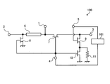
- 1 is a circuit diagram showing a high-frequency switch according to a first embodiment of the present invention.
- Equivalent circuit diagram at the time of reception without AGC operation of the high frequency switch according to the first embodiment Equivalent circuit diagram at the time of transmission and reception with AGC operation of the high frequency switch according to the first embodiment
- Equivalent circuit diagram at the time of reception without the AGC operation of the high frequency switch according to the second embodiment Equivalent circuit diagram at the time of transmission and reception with AGC operation of the high frequency switch according to the second embodiment Circuit diagram showing a high-frequency switch according to a third embodiment of the present invention.
- movement of the high frequency switch concerning Embodiment 3 Equivalent circuit diagram at the time of transmission and reception with AGC operation of the high frequency switch according to the third embodiment
- FIG. 1 is a circuit diagram showing a high-frequency switch 100 according to the first embodiment of the present invention.
- the high frequency switch 100 includes transistors 7, 8, 9, 10 that are field effect transistors, a resistor 11, a transmission line 6, and a control unit 101.
- the transistors 7, 8, 9, and 10 may be transistors other than field effect transistors.
- the control unit 101 is a control circuit that controls the gate voltages of the transistors 7, 8, 9, and 10.
- an input terminal 1 is connected to an antenna (not shown), an output terminal 3 that is a first output terminal is connected to an LNA (not shown), and an output terminal 2 that is a second output terminal is a termination (not shown). Connected to the container.
- the drain terminal of the transistor 7, which is the first transistor, is connected to a connection portion between the input terminal 1 and one end of the transmission line 6, and the source terminal of the transistor 7 is connected to the output terminal 3.
- the drain terminal of the transistor 8 is connected to the connection portion between the other end of the transmission line 6 and the output terminal 2, and the source terminal of the transistor 8 is grounded.
- the drain terminal of the transistor 9, which is the second transistor, is connected to the connection portion between the source terminal of the transistor 7 and the output terminal 3, and the source terminal of the transistor 9 is connected to the drain terminal of the transistor 10.
- the drain terminal of the transistor 10 as the third transistor is connected to the source terminal of the transistor 9, and the source terminal of the transistor 10 is grounded.
- One end of the resistor 11 is connected to a connection portion between the source terminal of the transistor 9 and the drain terminal of the transistor 10, and the other end of the resistor 11 is grounded.
- the transmission line 6 and the transistor 8 constitute a switching circuit connected between the input terminal 1 and the output terminal 2.
- the switching circuit is not limited to the configuration of the transmission line 6 and the transistor 8 as long as the switching circuit can be switched between a state of passing a transmission / reception signal between the input terminal 1 and the output terminal 2 and a state of blocking the transmission / reception signal.
- the control unit 101 controls whether the switching circuit is in a state of passing the transmission / reception signal or a state of blocking the transmission / reception signal. Specifically, the controller 101 switches the state of the switching circuit by controlling the gate voltage of the transistor 8.
- the control terminal 4 is connected to the gate terminals of the transistors 7, 8, and 10, and the control terminal 5 is connected to the gate terminal of the transistor 9.
- the control terminal 4 and the control terminal 5 are connected to the control unit 101.
- the control terminal turns on the transistor by applying a gate voltage equal to or higher than the pinch-off voltage to the gate terminal of the transistor, and turns the transistor off by applying a gate voltage lower than the pinch-off voltage.
- an on-state transistor can be equivalently regarded as a resistance, and hence this will be referred to as an on-resistance hereinafter. Since an off-state transistor can be regarded as a capacitor equivalently, it is hereinafter referred to as an off-capacitance.
- the high-frequency switch 100 shown in FIG. 1 turns on the transistors 7, 8, and 10 by controlling the gate voltage via the control terminal 4 and the control terminal 5 by the control unit 101 during reception without the AGC operation. At the same time, the transistor 9 is turned off. At this time, the switching circuit is in a state of blocking the transmission / reception signal. At the time of transmission and at the time of reception accompanied by AGC operation, the control unit 101 controls the gate voltage via the control terminal 4 and the control terminal 5, thereby turning off the transistors 7, 8, 10 and turning on the transistor 9 To. At this time, the switching circuit is in a state of passing the transmission / reception signal.
- control unit 101 includes a transistor The on state or off state of 7, 8, 9, 10 is switched according to the above.
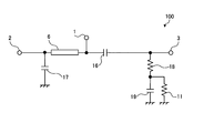
- FIG. 2 is an equivalent circuit diagram at the time of reception without the AGC operation of the high-frequency switch 100 according to the first embodiment.
- the transmission line 6 is set to have an electrical length of 90 ° at the center frequency of the transmission / reception signal, and transmission is performed if the on-resistance 13 of the transistor 8 is sufficiently smaller than the impedance of the terminator connected to the output terminal 2. Since the connection portion of the line 6 with the output terminal 2 can be regarded as a short circuit, and the impedance of the transmission line 6 viewed from the input terminal 1 can be approximated to infinity, the reception signal transmitted from the input terminal 1 to the output terminal 2 is blocked. Is done.
- the impedance of the off-capacitance 14 of the transistor 9 is set to be sufficiently high near the center frequency of the transmission / reception signal, and the reception signal is transmitted from the input terminal 1 to the output terminal 3.
- FIG. 3 is an equivalent circuit diagram at the time of transmission of the high frequency switch 100 according to the first embodiment and at the time of reception accompanied by the AGC operation.
- the impedance of the off-capacitance 16 of the transistor 7 is set to be sufficiently high in the vicinity of the center frequency of the transmission / reception signal, the input terminal 1 and the output terminal 3 are cut off.
- the impedance of the off-capacitance 17 of the transistor 8 is set to be sufficiently high near the center frequency of the transmission / reception signal, the transmission signal at the time of transmission can pass from the input terminal 1 to the output terminal 2.
- the transmission signal is transmitted from the input terminal 1 to the output terminal 2.
- the received signal is sufficiently attenuated and transmitted to the output terminal 3.
- the off-capacitance 19 of the transistor 10 is set so that the impedance is sufficiently high in the vicinity of the center frequency of the transmission / reception signal, the impedance when the high-frequency switch 100 is expected from the output terminal 3 is the on-resistance 18 of the transistor 9 and the resistor 11. Looks like it is terminated with a combined resistor. Therefore, by determining the value of the resistor 11 so that the combined resistance of the on-resistance 18 and the resistor 11 is equal to the characteristic impedance of the LNA, the high-frequency switch 100 viewed from the output terminal 3 is reduced in reflection.
- the impedance when the high frequency switch 100 is expected from the output terminal 3 to which the LNA is connected at the time of reception accompanied by the AGC operation seems to be terminated by the combined resistance of the transistor 9 and the resistor 11. Therefore, it is possible to obtain an effect of reducing reflection by the high-frequency switch 100 viewed from the output terminal 3 to which the LNA is connected without causing total reflection. That is, according to the high frequency switch 100 according to the first embodiment, the reflection of the signal from the output terminal 3 to the high frequency switch 100 at the time of transmission and reception can be made equal, and the reflection by the high frequency switch 100 viewed from the output terminal 3 is reduced. it can.
- the high frequency switch 100 it is possible to stably operate the LNA connected to the subsequent stage at the time of reception accompanied by the AGC operation, and the reception characteristics can be improved.
- the reception characteristics can be improved.
- it is not necessary to newly provide an AGC circuit it is possible to reduce the size by reducing the circuit scale.
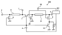
- FIG. FIG. 4 is a circuit diagram showing the high-frequency switch 200 according to the second embodiment of the present invention.
- the high frequency switch 200 includes a transistor 20 and a transmission line 21 that are fourth transistors in addition to the transistors 7, 8, 9, and 10, the resistor 11, and the transmission line 6 included in the high frequency switch 100. Further, the high frequency switch 200 includes a control unit 201 instead of the control unit 101. Below, the description of the same point as the high frequency switch 100 is omitted, and the different points will be mainly described.
- the source terminal of the transistor 7 is connected to one end of the transmission line 21.
- the other end of the transmission line 21 is connected to the output terminal 3. That is, the source terminal of the transistor 7 is connected to the output terminal 3 through the transmission line 21.
- the transmission line 21 is set to have an electrical length of 90 ° at the center frequency of the transmission / reception signal.
- the drain terminal of the transistor 20 is connected to the connection portion between the source terminal of the transistor 7 and the transmission line 21, and the source terminal of the transistor 20 is grounded.
- the drain terminal of the transistor 9 is connected to the connection portion between the other end of the transmission line 21 and the output terminal 3.
- the control terminal 50 is connected to the gate terminals of the transistors 9 and 20.
- the control terminal 4 and the control terminal 50 are connected to the control unit 201.
- the high-frequency switch 200 shown in FIG. 4 turns on the transistors 7, 8, and 10 when the control unit 201 controls the gate voltage via the control terminal 4 and the control terminal 50 during reception without an AGC operation.
- the transistors 9 and 20 are turned off.
- the switching circuit including the transmission line 6 and the transistor 8 is in a state of interrupting the transmission / reception signal.
- the control unit 201 controls the gate voltage via the control terminal 4 and the control terminal 50, thereby turning off the transistors 7, 8, 10 and turning off the transistors 9, 20 Turn on.
- the switching circuit including the transmission line 6 and the transistor 8 is in a state of passing a transmission / reception signal.
- control unit 201 includes a transistor The on state or off state of 7, 8, 9, 10, 20 is switched according to the above.
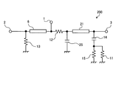
- FIG. 5 is an equivalent circuit diagram at the time of reception without the AGC operation of the high-frequency switch 200 according to the second embodiment.
- the transmission line 6 is set to have an electrical length of 90 ° at the center frequency of the transmission / reception signal, and transmission is performed if the on-resistance 13 of the transistor 8 is sufficiently smaller than the impedance of the terminator connected to the output terminal 2. Since the connection portion of the line 6 with the output terminal 2 can be regarded as a short circuit, and the impedance of the transmission line 6 viewed from the input terminal 1 can be approximated to infinity, the reception signal transmitted from the input terminal 1 to the output terminal 2 is blocked. Is done.
- the impedance of each of the off-capacitance 14 of the transistor 9 and the off-capacitance 25 of the transistor 20 is set to be sufficiently high in the vicinity of the center frequency of the transmission / reception signal, the received signal is input from the input terminal 1 to the output terminal 3. Is transmitted.
- FIG. 6 is an equivalent circuit diagram of the high frequency switch 200 according to the second embodiment at the time of transmission and at the time of reception accompanied by an AGC operation.
- the off-capacitance 16 of the transistor 7 and the off-capacitance 17 of the transistor 8 are set so that the impedance is sufficiently high in the vicinity of the center frequency of the transmission / reception signal, transmission transmitted from the input terminal 1 to the output terminal 3 during transmission is performed. The signal is blocked and the transmission signal is transmitted from the input terminal 1 to the output terminal 2. Further, the reception signal at the time of reception accompanied by the AGC operation is sufficiently attenuated and transmitted to the output terminal 3.
- the transmission signal leaked from the off-capacitance 16 of the transistor 7 is reflected because the on-resistance 29 of the transistor 20 is sufficiently small and can be regarded as a short circuit, so that the off-capacitance of the transistor 7 of the high-frequency switch 100 according to the first embodiment is reflected.
- the amount of isolation can be improved as compared with the case of blocking with only 16.
- the transmission line 21 of the high frequency switch 200 is set to have an electrical length of 90 ° at the center frequency of the transmission / reception signal, and the input impedance of the transmission line 21 viewed from the input terminal 1 can be approximated to infinity.
- the impedance of the off-capacitance 19 of the transistor 10 is set to be sufficiently high in the vicinity of the center frequency of the transmission / reception signal, the impedance when the high-frequency switch 200 is expected from the output terminal 3 is equal to the on-resistance 18 and the resistance of the transistor 9. It appears to be terminated by the combined resistance of the device 11.
- the high-frequency switch 200 according to the second embodiment can obtain the same effects as the high-frequency switch 100 according to the first embodiment, and can turn on the transistor 20 at the time of transmission or reception with an AGC operation.
- the resistance 29 provides an effect of improving the isolation amount as compared with the high frequency switch 100.
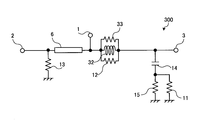
- FIG. 7 is a circuit diagram showing a high-frequency switch 300 according to the third embodiment of the present invention.
- the high frequency switch 300 includes an inductor 32 and a resistor 33 in addition to the transistors 7, 8, 9, 10 included in the high frequency switch 100, the resistor 11, the transmission line 6, and the control unit 101. Below, the description of the same point as the high frequency switch 100 is omitted, and the different points will be mainly described.
- One end of each of the inductor 32 and the resistor 33 is connected to the drain terminal of the transistor 7, and the other end of each of the inductor 32 and the resistor 33 is connected to the source terminal of the transistor 7. That is, both ends of the inductor 32 and the resistor 33 are connected to the drain terminal and the source terminal of the transistor 7.
- the high-frequency switch 300 shown in FIG. 7 controls the gate voltage via the control terminal 4 and the control terminal 5 when the signal is not accompanied by the AGC operation, so that the transistors 7, 8, and 10 are turned on. And the transistor 9 is turned off.
- the control unit 101 controls the gate voltage via the control terminal 4 and the control terminal 5, thereby turning off the transistors 7, 8, 10 and turning on the transistor 9 To.
- FIG. 8 is an equivalent circuit diagram at the time of signal reception without the AGC operation of the high frequency switch 300 according to the third embodiment.
- the transmission line 6 is set to have an electrical length of 90 ° at the center frequency of the transmission / reception signal, and transmission is performed if the on-resistance 13 of the transistor 8 is sufficiently smaller than the impedance of the terminator connected to the output terminal 2. Since the connection portion of the line 6 with the output terminal 2 can be regarded as a short circuit, and the impedance of the transmission line 6 viewed from the input terminal 1 can be approximated to infinity, the reception signal transmitted from the input terminal 1 to the output terminal 2 is blocked. Is done.
- the impedance of the off-capacitance 14 of the transistor 9 is set to be sufficiently high near the center frequency of the transmission / reception signal, and the reception signal is transmitted from the input terminal 1 to the output terminal 3. Since the on-resistance 12 of the transistor 7 is sufficiently small, the influence of the loss caused by the inductor 32 and the resistor 33 connected in parallel can be ignored.
- FIG. 9 is an equivalent circuit diagram of the high frequency switch 300 according to the third embodiment at the time of transmission and at the time of reception accompanied by an AGC operation.
- the off-capacitance 16 and the inductor 32 of the transistor 7 are set to resonate in parallel at the center frequency of the transmission / reception signal, the input terminal 1 and the output terminal 3 are cut off.
- the impedance of the off-capacitance 17 of the transistor 8 is set to be sufficiently high near the center frequency of the transmission / reception signal, the transmission signal at the time of transmission is transmitted from the input terminal 1 to the output terminal 2. Further, the reception signal at the time of reception accompanied by the AGC operation is sufficiently attenuated and transmitted to the output terminal 3.
- the resistor 33 connected in parallel to the resonance circuit composed of the off-capacitance 16 of the transistor 7 and the inductor 32 has a function of lowering the Q value of the resonance circuit to widen the isolation characteristic.
- the impedance of the resonance circuit composed of the off-capacitance 16 and the inductor 32 can be approximated to infinity, and the off-capacitance 19 of the transistor 10 is set to have a sufficiently high impedance in the vicinity of the center frequency of the transmission / reception signal.
- the impedance from which the high-frequency switch 300 is viewed from 3 appears to be terminated by the combined resistance of the on-resistance 18 of the transistor 9 and the resistor 11.
- the high-frequency switch 300 according to the third embodiment can obtain the same effect as the high-frequency switch 100 according to the first embodiment, and can be isolated by a resonance circuit including the off-capacitance 16 of the transistor 7 and the inductor 32. The effect of improving the amount of adjustment is obtained. Further, since the transmission line 21 used in the high-frequency switch 200 according to the second embodiment is unnecessary, there are advantages in that the circuit scale is reduced and the line loss is reduced as compared with the high-frequency switch 200.
- the configuration described in the above embodiment shows an example of the contents of the present invention, and can be combined with another known technique, and can be combined with other configurations without departing from the gist of the present invention. It is also possible to omit or change the part.
Landscapes
- Engineering & Computer Science (AREA)
- Computer Networks & Wireless Communication (AREA)
- Signal Processing (AREA)
- Electronic Switches (AREA)
- Transceivers (AREA)
- Waveguide Switches, Polarizers, And Phase Shifters (AREA)
Abstract
Description
図1は、本発明の実施の形態1にかかる高周波スイッチ100を示す回路図である。高周波スイッチ100は、電界効果トランジスタであるトランジスタ7,8,9,10と、抵抗器11と、伝送線路6と、制御部101と、を備える。なお、トランジスタ7,8,9,10は、電界効果トランジスタ以外のトランジスタであってもかまわない。制御部101は、トランジスタ7,8,9,10のゲート電圧を制御する制御回路である。
図4は、本発明の実施の形態2にかかる高周波スイッチ200を示す回路図である。高周波スイッチ200は、高周波スイッチ100が備えるトランジスタ7,8,9,10と、抵抗器11と、伝送線路6と、に加えて、第四のトランジスタであるトランジスタ20および伝送線路21を備える。また、高周波スイッチ200には、制御部101の代りに制御部201が備えられている。以下では、高周波スイッチ100と同様な点の説明は省いて、異なる点を主に説明する。
図7は、本発明の実施の形態3にかかる高周波スイッチ300を示す回路図である。高周波スイッチ300は、高周波スイッチ100が備えるトランジスタ7,8,9,10と、抵抗器11と、伝送線路6と、制御部101と、に加えて、インダクタ32および抵抗器33を備える。以下では、高周波スイッチ100と同様な点の説明は省いて、異なる点を主に説明する。
Claims (4)
- ドレイン端子が入力端子に接続され、ソース端子が第一の出力端子に接続された第一のトランジスタと、
ドレイン端子が前記第一の出力端子に接続された第二のトランジスタと、
ドレイン端子が前記第二のトランジスタのソース端子に接続され、ソース端子が接地された第三のトランジスタと、
一端が前記第二のトランジスタのソース端子と前記第三のトランジスタのドレイン端子との接続部に接続され、他端が接地された抵抗器と、
前記入力端子と第二の出力端子との間に接続され、前記入力端子と前記第二の出力端子との間の送受信信号を通過する状態と送受信信号を遮断する状態とに切替え可能な切替回路と、
前記第一のトランジスタ、前記第二のトランジスタ、前記第三のトランジスタおよび前記切替回路を制御する制御部と、
を備え、
前記制御部は、
自動利得制御動作を伴わない受信時には、前記切替回路を送受信信号を遮断する状態にして、前記第一のトランジスタおよび前記第三のトランジスタをオン状態にして、前記第二のトランジスタをオフ状態にし、
送信時および自動利得制御動作を伴う受信時には、前記切替回路を送受信信号を通過する状態にして、前記第一のトランジスタおよび前記第三のトランジスタをオフ状態にして、前記第二のトランジスタをオン状態にする
ことを特徴とする高周波スイッチ。 - 前記第一のトランジスタのソース端子が、前記送受信信号の中心周波数において電気長が90°になるように設定された伝送線路を介して前記第一の出力端子に接続されており、
前記第一のトランジスタのソース端子と前記伝送線路との接続部にドレイン端子が接続され、ソース端子が接地された第四のトランジスタをさらに備える
ことを特徴とする請求項1に記載の高周波スイッチ。 - 前記第一のトランジスタのドレイン端子およびソース端子に両端が接続されたインダクタをさらに備え、
前記第一のトランジスタのオフ容量と前記インダクタとが前記送受信信号の中心周波数で並列共振する
ことを特徴とする請求項1に記載の高周波スイッチ。 - 前記第一のトランジスタのドレイン端子およびソース端子に両端が接続された抵抗器をさらに備える
ことを特徴とする請求項3に記載の高周波スイッチ。
Priority Applications (3)
| Application Number | Priority Date | Filing Date | Title |
|---|---|---|---|
| EP18785220.7A EP3444890B1 (en) | 2017-04-10 | 2018-03-05 | High frequency switch |
| US16/499,622 US10700682B2 (en) | 2017-04-10 | 2018-03-05 | High-frequency switch |
| JP2019512382A JP6651056B2 (ja) | 2017-04-10 | 2018-03-05 | 高周波スイッチ |
Applications Claiming Priority (2)
| Application Number | Priority Date | Filing Date | Title |
|---|---|---|---|
| JP2017077619 | 2017-04-10 | ||
| JP2017-077619 | 2017-04-10 |
Publications (1)
| Publication Number | Publication Date |
|---|---|
| WO2018190034A1 true WO2018190034A1 (ja) | 2018-10-18 |
Family
ID=63792973
Family Applications (1)
| Application Number | Title | Priority Date | Filing Date |
|---|---|---|---|
| PCT/JP2018/008348 WO2018190034A1 (ja) | 2017-04-10 | 2018-03-05 | 高周波スイッチ |
Country Status (4)
| Country | Link |
|---|---|
| US (1) | US10700682B2 (ja) |
| EP (1) | EP3444890B1 (ja) |
| JP (1) | JP6651056B2 (ja) |
| WO (1) | WO2018190034A1 (ja) |
Families Citing this family (1)
| Publication number | Priority date | Publication date | Assignee | Title |
|---|---|---|---|---|
| US11955961B2 (en) * | 2021-10-12 | 2024-04-09 | Electronics And Telecommunications Research Institute | Switch circuit for ultra-high frequency band |
Citations (3)
| Publication number | Priority date | Publication date | Assignee | Title |
|---|---|---|---|---|
| JP2004172729A (ja) * | 2002-11-18 | 2004-06-17 | Hitachi Metals Ltd | アンテナ送受信切替え回路 |
| JP2012074890A (ja) * | 2010-09-28 | 2012-04-12 | Sumitomo Electric Device Innovations Inc | スイッチ及びスイッチの制御方法 |
| JP2013098771A (ja) | 2011-11-01 | 2013-05-20 | Mitsubishi Electric Corp | 高周波スイッチ |
Family Cites Families (1)
| Publication number | Priority date | Publication date | Assignee | Title |
|---|---|---|---|---|
| KR20130077432A (ko) * | 2011-12-29 | 2013-07-09 | 한국전자통신연구원 | 자동 이득 조절 귀환 증폭기 |
-
2018
- 2018-03-05 WO PCT/JP2018/008348 patent/WO2018190034A1/ja active Application Filing
- 2018-03-05 JP JP2019512382A patent/JP6651056B2/ja active Active
- 2018-03-05 EP EP18785220.7A patent/EP3444890B1/en active Active
- 2018-03-05 US US16/499,622 patent/US10700682B2/en active Active
Patent Citations (3)
| Publication number | Priority date | Publication date | Assignee | Title |
|---|---|---|---|---|
| JP2004172729A (ja) * | 2002-11-18 | 2004-06-17 | Hitachi Metals Ltd | アンテナ送受信切替え回路 |
| JP2012074890A (ja) * | 2010-09-28 | 2012-04-12 | Sumitomo Electric Device Innovations Inc | スイッチ及びスイッチの制御方法 |
| JP2013098771A (ja) | 2011-11-01 | 2013-05-20 | Mitsubishi Electric Corp | 高周波スイッチ |
Also Published As
| Publication number | Publication date |
|---|---|
| EP3444890A1 (en) | 2019-02-20 |
| US10700682B2 (en) | 2020-06-30 |
| US20200044651A1 (en) | 2020-02-06 |
| EP3444890A4 (en) | 2019-04-10 |
| EP3444890B1 (en) | 2019-09-11 |
| JP6651056B2 (ja) | 2020-02-19 |
| JPWO2018190034A1 (ja) | 2019-07-11 |
Similar Documents
| Publication | Publication Date | Title |
|---|---|---|
| US9037096B2 (en) | Reducing insertion loss in LNA bypass mode by using a single-pole-triple-throw switch in a RF front end module | |
| US7893791B2 (en) | Gallium nitride switch methodology | |
| US8306481B2 (en) | Single pole multi throw switch | |
| US8416032B2 (en) | Semiconductor switch, transceiver, transmitter, and receiver | |
| JP2015226313A (ja) | スイッチ回路付き利得可変型増幅器 | |
| JP2006025062A (ja) | 高周波スイッチ回路 | |
| US20080174357A1 (en) | Semiconductor device | |
| US20150381168A1 (en) | High frequency switching circuit | |
| US8532584B2 (en) | RF switches | |
| WO2018159428A1 (ja) | 増幅回路 | |
| JP2010056876A (ja) | デュプレクサ回路 | |
| WO2018190034A1 (ja) | 高周波スイッチ | |
| US8909171B2 (en) | RF antenna switch circuit, high frequency antenna component, and mobile communication device | |
| JP5094515B2 (ja) | ミリ波帯スイッチ | |
| EP1739827B1 (en) | Radio frequency receiver including a limiter and related methods | |
| US7728656B2 (en) | Signal input circuit | |
| US20090131001A1 (en) | Switch architecture | |
| KR20140086487A (ko) | 고주파 스위치 회로 | |
| JP4063230B2 (ja) | 高周波スイッチ | |
| WO2022259442A1 (ja) | 高周波スイッチ | |
| JP2008017170A (ja) | 半導体スイッチ回路並びに通信機器 | |
| JP6797041B2 (ja) | 低雑音増幅器 | |
| US20140062831A1 (en) | Switching circuit | |
| JP2024008472A (ja) | レーダー用リミタ回路及びレーダー装置 | |
| KR101963268B1 (ko) | 고주파 스위치 |
Legal Events
| Date | Code | Title | Description |
|---|---|---|---|
| WWE | Wipo information: entry into national phase |
Ref document number: 2018785220 Country of ref document: EP |
|
| ENP | Entry into the national phase |
Ref document number: 2018785220 Country of ref document: EP Effective date: 20181113 |
|
| 121 | Ep: the epo has been informed by wipo that ep was designated in this application |
Ref document number: 18785220 Country of ref document: EP Kind code of ref document: A1 |
|
| ENP | Entry into the national phase |
Ref document number: 2019512382 Country of ref document: JP Kind code of ref document: A |
|
| NENP | Non-entry into the national phase |
Ref country code: DE |