WO2018186408A1 - 磁界発生回路 - Google Patents
磁界発生回路 Download PDFInfo
- Publication number
- WO2018186408A1 WO2018186408A1 PCT/JP2018/014293 JP2018014293W WO2018186408A1 WO 2018186408 A1 WO2018186408 A1 WO 2018186408A1 JP 2018014293 W JP2018014293 W JP 2018014293W WO 2018186408 A1 WO2018186408 A1 WO 2018186408A1
- Authority
- WO
- WIPO (PCT)
- Prior art keywords
- circuit
- magnetic field
- coil
- voltage
- field generation
- Prior art date
- Legal status (The legal status is an assumption and is not a legal conclusion. Google has not performed a legal analysis and makes no representation as to the accuracy of the status listed.)
- Ceased
Links
Images

















Classifications
-
- H—ELECTRICITY
- H01—ELECTRIC ELEMENTS
- H01Q—ANTENNAS, i.e. RADIO AERIALS
- H01Q7/00—Loop antennas with a substantially uniform current distribution around the loop and having a directional radiation pattern in a plane perpendicular to the plane of the loop
- H01Q7/06—Loop antennas with a substantially uniform current distribution around the loop and having a directional radiation pattern in a plane perpendicular to the plane of the loop with core of ferromagnetic material
-
- H—ELECTRICITY
- H03—ELECTRONIC CIRCUITRY
- H03K—PULSE TECHNIQUE
- H03K17/00—Electronic switching or gating, i.e. not by contact-making and –breaking
- H03K17/51—Electronic switching or gating, i.e. not by contact-making and –breaking characterised by the components used
- H03K17/56—Electronic switching or gating, i.e. not by contact-making and –breaking characterised by the components used by the use, as active elements, of semiconductor devices
- H03K17/687—Electronic switching or gating, i.e. not by contact-making and –breaking characterised by the components used by the use, as active elements, of semiconductor devices the devices being field-effect transistors
Definitions
- the present invention relates to a magnetic field generation circuit that generates a magnetic field for communication.
- a communication system called a keyless entry system is widely used to remotely unlock and lock a door of an automobile or the like. Also, in recent years, a short distance called a passive entry system or a smart entry system that uses a magnetic field signal in the VLF band or LF band that is automatically unlocked when the remote control is close to the vehicle and is automatically locked when the remote controller is left. Communication systems are widespread.
- a VLF band or LF band magnetic field signal is transmitted from the vehicle side, and a radio wave signal of a high frequency (RF band) is received from a remote controller that receives the signal.
- RF band radio wave signal of a high frequency
- a coil antenna In a magnetic field signal transmission circuit, a coil antenna is used in which an inductor (coil) and a capacitor having a constant such that the signal frequency of the communication system is equal to the series resonance frequency are connected in series.
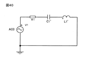
- FIG. 40 shows an example of such a magnetic field signal transmission circuit.
- a large coil current can flow even at a low voltage.
- a large magnetic field output can be obtained.
- Such a combination of a coil antenna and a drive system is particularly suitable for a short-range communication system using a magnetic field, and is employed in almost all passive keyless entry systems.
- the resonance current has a frequency characteristic having a peak at the resonance frequency, and it takes time for the current value to reach the maximum value.
- the series resonance circuit has a frequency characteristic in which the current has a maximum peak at the resonance frequency (in general, the frequency steep characteristic of the resonance circuit is expressed by a Q value). It is difficult to perfectly match the resonance frequency of the product with the driving frequency due to component variations and the like, and if this is the case, small characteristic variations of the product will cause a large difference in resonance current, making it difficult to use. Therefore, a resistor R1 (hereinafter referred to as “damping resistor”) is connected in series with the LC circuit (see FIG. 40). As a result, the above-mentioned Q value is lowered, and the frequency current characteristic is flattened to improve usability.
- a resistor R1 hereinafter referred to as “damping resistor”
- the time until the resonance current increases to the maximum value (hereinafter referred to as “rise time”) is approximately L1 ′. Proportional to / R1. In the passive keyless entry system, this rise time is an important factor that determines the communication speed. By connecting the above-described damping resistor, the rise time can be shortened.
- the value of the damping resistor is comprehensively determined from the frequency characteristics of the resonance current required by the system, the rise time, and the L and C characteristic values.
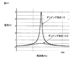
- FIG. 41 shows the frequency characteristics of the input current when R1 is 1 ⁇ and 10 ⁇ , respectively
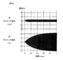
- FIG. 42 shows the current transient characteristics.
- FIG. 41 shows that the frequency characteristic of the input current is very peaky when the damping resistance R1 is 1 ⁇ . In actual use, it is very difficult to adjust the change of the current value due to the characteristic variation of the LC circuit by the driving circuit, and the current value is stabilized by the limitation by the damping resistor.
- the damping resistor is an indispensable part in the coil antenna drive system used in the magnetic field communication system in the VLF band and the LF band.
- the communication distance between the vehicle and the remote control key has been used at about 1 m.
- a longer distance for example, a use in which the communication distance is extended to about 10 m has been required. It was.
- a welcome light function that notifies the position of the vehicle by blinking a lamp when the remote control holder approaches, a walk-away lock that automatically locks when about 10 meters away, and confirmed that the owner is at a short distance of about 10 meters
- the following method can be considered. 1) Increase the coil current value (the spatial magnetic field strength is almost proportional to the current value). 2) Increase the coil inductance (the spatial magnetic field strength is approximately proportional to the square root of the inductance ratio). 3) The coil core is lengthened (the spatial magnetic field strength is approximately proportional to the length of the coil core).
- the damping resistance value cannot be reduced due to the resonance characteristic of the current value and the rise time reduction, Also, the input voltage value is determined from the vehicle system voltage and cannot usually be raised easily. Even if the voltage can be increased, it is necessary to increase the current capacity of the damping resistor because the loss in the damping resistor increases with the square of the current value.
- the method of increasing the magnetic flux density by lengthening the coil core of 3) is generally used.
- a magnetic field required by the system can be generated with a core having a length of 40 to 80 mm.
- a core having a length of more than 200 mm is required for 10 m of medium-distance communication. For this reason, various problems such as an increase in cost, a decrease in productivity, an increase in parts installation space, and a decrease in product reliability occur.
- the intensity of the resonance current is determined by the degree of resonance, that is, the interrelationship between the resonance frequency, the Q value and the drive frequency of the circuit. Therefore, in order to control the magnetic field generated in the space, it is necessary to configure a so-called current control circuit that detects the current flowing through the coil and adjusts the output voltage of the circuit. This complicates the circuit configuration and may increase the cost.
- the antenna system using the series resonance phenomenon has the above-described problems.
- the present invention provides a magnetic field generation circuit that generates a magnetic field suitable for a communication device in a keyless entry system, for example.
- a magnetic field generation circuit includes a transformer antenna that generates a magnetic field, and an AC power supply circuit that supplies an AC voltage as a drive voltage to a primary coil of the transformer antenna.
- the transformer antenna includes a transformer including a primary coil and a secondary coil, and a resonant capacitor connected in parallel to the secondary coil of the transformer.
- the resonance frequency of the parallel resonance circuit composed of the secondary coil and the resonance capacitor is set equal to the frequency of the AC voltage supplied from the AC power supply circuit.
- a magnetic field generation circuit includes a step-up transformer including a primary coil and a secondary coil, a parallel resonant coil antenna that generates a magnetic field, and an AC power supply circuit that supplies an AC voltage as a drive voltage to the step-up transformer.
- the parallel resonant coil antenna includes a third coil and a resonant capacitor connected in parallel to the third coil.
- the resonance frequency of the resonance circuit composed of the secondary coil and the parallel resonance coil antenna is set equal to the frequency of the AC voltage supplied from the AC power supply circuit.
- a magnetic field generation circuit includes a first coil, a parallel resonance coil antenna that generates a magnetic field, and an AC power supply circuit that supplies a rectangular wave AC voltage as a drive voltage to the parallel resonance coil antenna.
- the parallel resonant coil antenna includes a second coil and a resonant capacitor connected in parallel to the second coil.
- the resonance frequency of the parallel resonance coil antenna is set equal to the frequency of the AC voltage supplied from the AC power supply circuit.
- the figure which shows the structural example (transformer antenna and sine wave alternating current power supply) of the magnetic field generation circuit in Embodiment 1 of this invention The figure which shows the structure of the transformer antenna in embodiment of this invention The figure which showed the comparison of the measured value with respect to various items by each of the conventional magnetic field generation circuit and the magnetic field generation circuit of Embodiment 1
- the figure which shows the structural example of the magnetic field generator circuit in Embodiment 3 of this invention The figure which shows the structural example of the magnetic field generator circuit in Embodiment 3 of this invention.
- Timing chart of switch element in drive circuit of magnetic field generation circuit in embodiment 3 The figure which shows the simulation result with respect to the magnetic field generator circuit of Embodiment 3.
- the figure which shows the simulation result (various current waveforms) with respect to the magnetic field generator circuit of Embodiment 3.
- the figure which shows the measurement result with respect to the magnetic field generator circuit of Embodiment 3, and the conventional magnetic field generator circuit The figure which shows the measurement result with respect to the magnetic field generator circuit of Embodiment 3.
- FIG. 17 shows another configuration example of the magnetic field generation circuit in the thirteenth embodiment.
- FIG. 17 shows another configuration example of the magnetic field generation circuit in the thirteenth embodiment.
- FIG. 17 shows another configuration example of the magnetic field generation circuit in the thirteenth embodiment.
- FIG. 18 shows a configuration example (including a discharge resistor) of a magnetic field generation circuit in the fifteenth embodiment.
- FIG. 17 shows another configuration example of the magnetic field generation circuit in the fifteenth embodiment.
- FIG. 17 shows another configuration example of the magnetic field generation circuit in the fifteenth embodiment.
- FIG. 17 shows another configuration example of the magnetic field generation circuit in the fifteenth embodiment.
- the figure which shows the structure of the magnetic field generation circuit using the conventional series resonance The figure which shows the frequency characteristic of the input current in the conventional magnetic field generator circuit shown in FIG.
- the figure which shows the current transient characteristic of the input current in the conventional magnetic field generation circuit shown in FIG. Diagram showing the configuration of a basic parallel resonant circuit
- Fig. 43 shows a basic parallel resonant circuit.
- a coil L1 'formed by winding a coil around an open magnetic circuit core and a capacitor C1' are connected in parallel to an AC power supply AC.
- the drive voltage is 130 V (from peak to peak) to satisfy this requirement. It is necessary to apply a sine wave voltage of However, it is very difficult to realize such a high voltage drive system in an in-vehicle system.
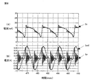
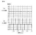
- FIGS. 44 and 45 show simulation waveforms when a sine wave voltage and a rectangular wave voltage are applied to a parallel resonance circuit of a coil L1 ′ having an inductance of 165 ⁇ H and a capacitor C1 ′ having a capacitance of 10 ⁇ F. . 44 shows the waveform of the coil current flowing in the input current (FIG.
- FIG. 30B shows waveforms of an input current and a coil current when a rectangular wave voltage of 125 kHz and 130 V (value from peak to peak) is applied to the parallel resonant circuit.
- FIG. 44 shows waveforms of an input current and a coil current when a rectangular wave voltage of 125 kHz and 130 V (value from peak to peak) is applied to the parallel resonant circuit. Referring to FIG. 44, it can be seen that when a sinusoidal voltage is applied, a coil current is generated due to resonance.
- a magnetic field generation circuit magnetic field communication circuit
- Such a magnetic field generation circuit is useful, for example, in a communication device that generates a magnetic field signal in a VLF band or an LF band that is applied to a keyless entry system of an automobile.
- FIG. 1 is a diagram showing a configuration of a magnetic field generation circuit according to Embodiment 1 of the present invention.
- the magnetic field generation circuit constitutes an AC power supply circuit AC1 that generates a sinusoidal AC voltage, a transformer Tx1 including a primary coil L1 and a secondary coil L2, and a secondary coil L2 of the transformer Tx1 and a resonance circuit. And a resonant capacitor C1.
- the transformer Tx1 is configured by winding a primary coil L1 and a secondary coil L2 around the outer periphery of an open magnetic circuit core Co (bar-shaped core).
- a resonant capacitor C1 is connected in parallel to the secondary coil L2 of the transformer Tx1.
- the secondary coil L2 of the transformer Tx1 and the resonance capacitor C1 constitute a parallel resonance circuit.
- the resonance frequency of the parallel resonance circuit is set to be equal to the drive frequency by the AC power supply circuit AC1. For this reason, the inductance (L2) of the secondary coil L2 and the capacitance (C1) of the capacitor C1 are set to values such that the resonance frequency is equal to the drive frequency.
- the ratio of the number of turns of the primary coil L1 and the secondary coil L2 is set so that a desired output voltage of the secondary coil L2 can be obtained with respect to the input voltage to the primary coil L1.
- the transformer Tx1 and the resonant capacitor C1 function as a magnetic field generating antenna having a transformer structure.
- an antenna constituted by the transformer Tx1 and the resonant capacitor C1 is referred to as a “transformer antenna” At1.
- the resonance frequency of the parallel resonance circuit composed of the secondary coil L2 and the resonance capacitor C1 and the drive frequency which is the frequency of the AC voltage supplied from the AC power supply circuit AC1 are not necessarily equal to each other. It is not necessary to set, for example, it may be set to a value that is equal within a range of ⁇ 10%.
- AC power supply circuit AC1 for supplying a sine wave voltage is connected to primary coil L1 of transformer antenna At1.
- the AC power supply circuit AC1 applies a sine wave voltage having a predetermined drive frequency to the primary coil L1 of the transformer antenna At1.
- the transformer antenna At1 generates a sine wave current in the secondary coil L2, and generates an alternating magnetic field.
- AC power supply circuit AC1 functions as a drive circuit for transformer antenna At1.
- the magnetic field generation circuit of the present embodiment having the above-described configuration uses the parallel resonance phenomenon, the rise time of the coil current is short, and there is little variation due to the frequency of the resonance current value.
- the damping resistor necessary for the series resonance circuit is not necessary. For this reason, there is no loss in the damping resistor, and the efficiency of the circuit is improved. Further, since there are no restrictions such as damping resistance and current rise time, the upper limit of the coil current is limited only to power and loss.
- the output voltage and resonance current of the secondary coil L2 can be optimized. For example, it is possible to operate at the most suitable coil-capacitor voltage in consideration of the voltage resistance of the resonant capacitor and the coil itself.
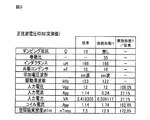
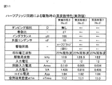
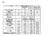
- FIG. 3 shows a comparison of measured values for various assumed items by the conventional magnetic field generation circuit (FIG. 34) and the magnetic field generation circuit of the present embodiment (FIG. 1).
- the secondary coil / primary coil turns ratio N2 / N1 35
- the length of the open magnetic circuit core Co is 90 mm.
- the measurement data is a value at the resonance frequency of each antenna.
- the input current is 21% of the conventional value and the spatial magnetic flux density is 172% of the conventional value, and the efficiency and output are greatly improved.
- parallel resonance there is a basic characteristic that the coil resonance current is constant and only the input current is reduced in accordance with the degree of LC parallel resonance. It is easy to keep the density constant.
- the magnetic field generation circuit of the present embodiment uses a parallel resonance phenomenon.
- the effect of using the parallel resonance phenomenon is that constant output, high speed, and high efficiency and high power can be achieved by eliminating the damping resistor.
- Parallel resonance has the basic characteristic that the coil resonance current is constant and only the input current decreases according to the degree of parallel resonance, and it is easy to keep the spatial magnetic flux density constant regardless of the degree of resonance.
- a damping resistor such as a resonance circuit is not necessary.
- the magnetic field generation circuit of the present embodiment since parallel resonance is used, the rise time of the coil current can be shortened, and variation due to the frequency of the resonance current value can be reduced. For this reason, a damping resistor is not required, loss at the damping resistor can be reduced, and circuit efficiency is improved. Also, by setting the transformer turns ratio and the inductance value to appropriate values, it becomes possible to set the output voltage and resonance current of the secondary coil to suitable values. For example, it is possible to operate at a suitable coil-capacitor voltage in consideration of the voltage resistance of the resonant capacitor and the coil itself. Further, it is possible to increase the magnetic field output by increasing the coil current without increasing the length of the open magnetic circuit core Co. Alternatively, the size can be reduced at the same output as the conventional method.
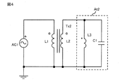
- FIG. 4 is a diagram showing a configuration of the magnetic field generation circuit according to the second embodiment of the present invention.
- the magnetic field generation circuit according to the present embodiment includes an AC power supply circuit AC1 that supplies a sine wave voltage, a step-up transformer Tx2, and a parallel resonant coil antenna At2.
- the parallel resonance coil antenna At2 includes a coil L3 and a resonance capacitor C1 connected in parallel to the coil L3.
- the coil L3 performs a function equivalent to the function of the leakage inductance component in the transformer Tx1 of the transformer antenna At1.
- the secondary coil L2 is connected in parallel with the parallel resonant coil antenna At2, and the primary coil L1 is connected to the AC power supply circuit AC1 that is a drive circuit.
- the parallel resonance frequency of the circuit composed of the secondary coil L2 of the step-up transformer Tx2 and the parallel resonance coil antenna At2 is set to be equal to the drive frequency that is the frequency of the AC voltage supplied by the AC power supply circuit AC1.
- the parallel resonance frequency of the circuit composed of the secondary coil L2 of the step-up transformer Tx2 and the parallel resonance coil antenna At2 and the drive frequency of the AC voltage supplied from the AC power supply circuit AC1 are set to be strictly equal. It is not necessary to set, for example, so as to be equal within a range of ⁇ 10%.
- step-up transformer Tx2 converts the input voltage in accordance with the turn ratio of the primary coil L1 and the secondary coil L2, supplies it to the parallel resonant coil antenna At2, and thereby generates an alternating magnetic field from the parallel resonant coil antenna At2.
- the magnetic field generation circuit of the present embodiment having the above configuration has the same effects as those of the first embodiment and further has the following effects. Since boosting is performed by the dedicated transformer Tx2, the existing coil antenna can be used. Further, since the coil input voltage can be adjusted by the turn ratio (step-up ratio) by a closed magnetic circuit transformer having good coupling, the coil current can be easily adjusted. In the first embodiment, the voltage applied to the LC parallel resonant circuit is boosted by the transformer function of the transformer antenna. On the other hand, in the present embodiment, the same function is realized by raising the voltage with a dedicated step-up transformer. Since other operations and functions are the same as those in the first embodiment, description thereof is omitted here.
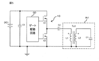
- FIG. 5 is a diagram showing the configuration of the magnetic field generation circuit according to the third embodiment of the present invention.
- the magnetic field generation circuit in the present embodiment includes a transformer antenna At1, a DC power supply DC1, and a half bridge circuit 10 as a drive circuit for driving the transformer antenna At1.
- the DC power supply DC1 and the half bridge circuit 10 (drive circuit) constitute an AC power supply circuit that outputs a rectangular wave AC voltage.
- the half-bridge circuit 10 includes an input capacitor C3, two switch elements Q1 and Q2 connected in series, and a gate drive circuit GD that controls the switch elements Q1 and Q2.
- the switch elements Q1 and Q2 are composed of, for example, FETs.
- the transformer antenna At1 is the same as that described in the first embodiment.
- the primary coil L1 of the transformer antenna At1 and the output terminal of the half bridge circuit 10 are connected. More specifically, the high voltage side terminal of the primary coil L1 of the transformer antenna At1 is connected to a connection point between the switch elements Q1 and Q2 via the bypass capacitor C2.
- the half-bridge circuit 10 receives a DC voltage from the DC power source DC1 via the input capacitor C3, converts the input DC voltage into a desired rectangular wave voltage, and supplies the voltage to the transformer antenna At1. Specifically, the half-bridge circuit 10 drives the two switch elements Q1 and Q2 in opposite phases (exclusively) and at a predetermined frequency with a predetermined on-duty ratio, thereby providing a DC power source DC1.
- a rectangular wave voltage having a predetermined driving frequency is generated from the first coil L1 and applied to the primary coil L1 of the transformer antenna At1. As a result, a sinusoidal resonance current is generated in the secondary coil L2, and an alternating magnetic field is generated in the space.
- the on-duty ratio of the switching element is set to a value within the range of 10% to 45%.
- the on-duty ratio of the switching element may be set to a value within the range of 10% to 40%. More preferably, the on-duty ratio may be set to a value within the range of 10% to 20%.
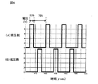
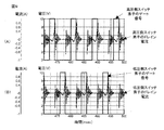
- FIGS. 6A and 6B are timing charts of the switch elements Q1 and Q2 on the high voltage side and the low voltage side, respectively. For example, as shown in FIG. 6, the off duty ratio is set to 75%, that is, the on duty ratio is set to 25%.
- the inventor has found that by setting the duty ratio in such a range, a parallel resonant operation by a rectangular wave voltage becomes possible. Further, the present inventor significantly attenuates the current peak value output from the half-bridge circuit 10 by appropriately setting and utilizing the leakage inductance between the primary coil L1 and the secondary coil L2 of the transformer antenna At1. I found it possible. As a result, a highly efficient sinusoidal resonance current can be generated.
- the on-duty ratio of the switch element of the half bridge circuit is set to an appropriate value, here 10% to 45%.
- the on-duty ratio is set to 25%
- the high-voltage side switch Q1 is short-circuited (on) at 25%
- the low-voltage side switch element Q2 is 25%
- the primary coil L1 is used for the remaining 50% period.
- the leakage inductance generated between the primary coil and the secondary coil of the transformer antenna it becomes possible to limit the maximum peak current flowing from the drive circuit to the transformer antenna.
- the transformer antenna allows high voltage to be applied to the secondary resonance system, and the combination of these four elements (high voltage by the transformer antenna, circuit capable of realizing free vibration period, setting of free vibration period, appropriate leakage inductance) For the first time, it was possible to realize a spatial magnetic field generation circuit using a practical parallel resonance phenomenon.
- FIG. 7 shows a simulation result for the configuration of the magnetic field generation circuit in the present embodiment.
- a simulation was performed when a rectangular wave voltage was applied with an on-duty of 25%.
- FIG. 8 shows an input current (circuit input current) Iin from the DC power source to the half-bridge circuit 10, an input current to the transformer Tx1 (hereinafter referred to as “transformer input current”) Itr, and a resonant current (hereinafter referred to as “transistor current”)
- Transformer input current an input current to the transformer Tx1
- transistor current a resonant current
- FIG. 9 shows simulation results of drain currents and gate signal waveforms of the high-voltage side switch element Q1 and the low-voltage side switch element Q2.
- the coil resonance current Icoil of the secondary coil L2 has a sine wave, but the transformer input current Itr has a waveform different from that of the sine wave.
- the transformer input current Itr is a current for supplying from the half-bridge circuit 10 an amount of attenuation of the secondary resonance current due to resistance loss, LC resonance frequency and drive frequency deviation, or the like. The value of this current is determined by the difference between the voltage supplied from the switch elements Q1 and Q2 and the voltage excited from the secondary resonance current, and becomes smaller as the LC parallel resonance frequency and the drive frequency become closer.
- the circuit input current Iin (mA order) is extremely small with respect to the transformer input current Itr (A order).
- Most of the drain current of the switch element Q1 on the high voltage side in FIG. 8 is supplied from the input capacitor C3 (see FIG. 5), and the negative portion of the drain current is the current regenerated in the input capacitor C3.
- the drain current of the switch element Q2 on the low voltage side is supplied from the coil resonance current Icoil of the secondary coil, and no energy is supplied from the half bridge circuit.
- the current used in this circuit is only the positive current minus the negative current of the drain current of the switch element Q1 on the high voltage side.
- the circuit input current is reduced to 23% in sample # 2 and to 42% in sample # 3.
- the spatial magnetic flux density was significantly increased to 177% for sample # 2 and 286% for sample # 3.
- the rise time of magnetic flux density was comparable as the conventional one.
- the circuit input current Iin is 0.147 A (effective value), and the coil resonance current Icoil is 0.357 A (effective value). Therefore, in the conventional method, the coil resonance current Icoil is about 2.4 times the circuit input current Iin.
- the circuit input current Iin is 0.034 A (effective value), and the coil resonance current Icoil is 0.665 A (effective value). Therefore, the coil resonance current Icoil is about 20 times the circuit input current Iin.
- the circuit input current Iin is 0.062 A (effective value), and the coil resonance current Icoil is 0.665 A (effective value). Therefore, the coil resonance current Icoil is about 10.7 times the circuit input current Iin.
- FIG. 11 shows an actual measurement value of the frequency characteristic in the sample # 2 when the drive frequency is changed.
- the drive frequency is varied, there is almost no difference in the output magnetic flux density, and it can be confirmed that the frequency characteristics of the output magnetic flux are extremely stable.
- the maximum value / minimum value was 3.5 times. It was confirmed that fluctuation was suppressed in the resonance system in which resistance components such as damping resistance were eliminated as much as possible.
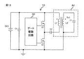
- FIGS. 12 to 14 show other examples of connection of the half bridge circuit to the transformer antenna At1.
- the bypass capacitor C2 is inserted between the low voltage side end of the primary coil L1 and the low voltage side output end of the half bridge circuit.
- the transformer antenna At1 is connected in parallel to the high-voltage side switch element Q1, and the bypass capacitor C2 is inserted between the low-voltage side end of the primary coil L1 and the low-voltage side end of the switch element Q1.
- FIG. 14 the transformer antenna At1 is connected in parallel to the high-voltage side switch element Q1, and the bypass capacitor C2 is inserted between the high-voltage side end of the primary coil L1 and the high-voltage side end of the switch element Q1. .
- the magnetic field generation circuit having the configuration described above has the following effects in addition to the effects described in the first embodiment. That is, it is possible to drive a parallel resonant circuit by a half-bridge circuit that is difficult in the prior art and has a simple configuration and simple control. For this reason, the convenience as a system can be improved and the cost can be reduced. In addition, due to the regenerative current from the transformer side and the self-excited resonance operation in the operation section of the low-voltage side switch element, the current actually supplied to the drive circuit can be extremely reduced, and the efficiency can be improved. Moreover, it becomes possible to reduce the input current variation due to the frequency variation. As a result, it is possible to realize a highly efficient circuit with little difference due to frequency variation of the input current.
- the half bridge circuit is used as the drive circuit for driving the transformer antenna At1, but this drive circuit is not limited to the half bridge circuit, and other types of drive circuits may be used.
- the half bridge circuit 10 may be changed to a full bridge circuit.
- FIG. 15 shows a configuration in which a full bridge circuit is applied as a drive circuit for the transformer antenna At1.
- the full bridge circuit 12 includes an input capacitor C3, four switch elements Q1 to Q4, and a gate drive circuit GD that controls the switch elements Q1 to Q4.
- the switch elements Q1 and Q2 are connected in series, and the switch elements Q3 and Q4 are connected in series.
- the series circuit of switch elements Q1 and Q2 and the series circuit of switch elements Q3 and Q4 are connected in parallel.
- the transformer antenna At1 is the same as that described in the first embodiment.
- the connection point between the switch element Q1 and the switch element Q2 is connected to the high voltage side end of the primary coil L1 of the transformer antenna At1, and the connection point between the switch element Q3 and the switch element Q4 is the low voltage side end of the primary coil L1 of the transformer antenna At1. Connected to.
- the full bridge circuit 12 receives a direct current voltage from the direct current power source DC1 via the input capacitor C3, and drives the switch elements Q1 to Q4 to turn on and off. Generate voltage.
- the generated rectangular wave AC voltage is applied to the primary coil L1 of the transformer antenna At1, thereby generating a sinusoidal resonance current in the secondary coil L2 and generating an AC magnetic field in the space.
- the full-bridge circuit 12 is also driven by setting the on-duty ratios of the switch elements Q1, Q2, Q3, and Q4 to appropriate values, here 10% to 45%. .
- an AC voltage having an amplitude twice that of the voltage (that is, the circuit input voltage) supplied from the DC power source DC1 is applied to the primary coil L1 of the transformer antenna At1. Since the transformer antenna At1 has a function as a “transformer”, if the input voltage is doubled, the output voltage is also doubled. For this reason, this configuration can easily increase the coil current, that is, the spatial magnetic flux density. If adjustment is made so that the output voltage does not change by changing the specifications of the transformer antenna At1, the current per switch element Q1 to Q4 is about 1 ⁇ 2, so the current value required for the switch elements Q1 to Q4 decreases. Therefore, it is possible to use a switch element having a specification with lower performance (that is, inexpensive).
- FIG. 16 shows the simulation results of the current waveforms of the circuit input current Iin, the transformer input current Itr, and the secondary coil L2 coil resonance current Icoil from the DC power supply DC1 to the gate drive circuit GD.
- FIG. 17 shows the simulation result.
- the simulation calculation by the configuration of the third embodiment is also shown for comparison.
- the ratio of the input current to the full bridge circuit 12 is about 340%.
- the input current ratio to the transformer antenna At1 is only 140%. This indicates that the current bridge values of the switching elements Q1 to Q4 are reduced by the full bridge circuit 12.
- the spatial magnetic flux density ratio is 198% and is greatly increased. From the above, it has been confirmed that the combination of the transformer antenna At1 and the full bridge circuit 12 has a great effect in reducing the current value of the currents of the switch elements Q1 to Q4 and increasing the spatial magnetic flux density.
- the voltage applied to the primary coil L1 is substantially doubled with respect to the voltage of the DC power supply DC1. From this, it becomes possible to further increase the coil output current. On the contrary, when the coil current output is made equal, the maximum drain current for each switch element can be halved, and a low-performance switch element or IC can be used. Selection becomes easy.
- a double forward circuit may be used instead of the half bridge circuit 10 as a drive circuit for the transformer antenna At1.
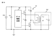
- FIG. 18 shows a configuration in which a double forward circuit is applied as a drive circuit for the transformer antenna At1.
- the double forward circuit 14 includes an input capacitor C3, a series circuit of a switch element Q1 and a diode, a series circuit of a diode D2 and a switch element Q2, and a gate drive circuit GD that controls the switch elements Q1 and Q2.
- the series circuit of the switch element Q1 and the diode D1 and the series circuit of the diode D2 and the switch element Q2 are connected in parallel.
- the transformer antenna At1 is the same as that described in the first embodiment.
- the connection point between the switch element Q1 and the diode D1 is connected to the high-voltage side end of the primary coil L1 of the transformer antenna At1.
- a connection point between the diode D2 and the switch element Q2 is connected to a low voltage side end of the primary coil L1 of the transformer antenna At1.
- the double forward circuit 14 When the transformer antenna At1 is driven, the double forward circuit 14 performs substantially the same operation as that performed by the half bridge circuit 10 of the third embodiment. That is, the double forward circuit 14 is also driven by setting the on-duty ratio of the switch elements Q1 and Q2 to an appropriate value (here, 10% to 45%).
- the configuration according to the present embodiment also provides the same effects as the configuration of the third embodiment.
- a push-pull circuit may be used in place of the half-bridge circuit 10 as a drive circuit for the transformer antenna At1.
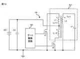
- FIG. 19 shows a configuration in which the push-pull circuit 16 is applied as a drive circuit for the transformer antenna At1.
- the push-pull circuit 16 includes an input capacitor C3, switch elements Q1 and Q2, and a gate drive circuit GD that controls the switch elements Q1 and Q2.
- the transformer Tx11 of the transformer antenna At1 includes a first coil portion L11 and a second coil portion L12 as primary coils.
- the switch element Q2 is connected in series with the second coil portion L12 on the low voltage side of the second coil portion L12.
- the switch element Q1 is connected in parallel to a series circuit including the primary coil L1 and the switch element Q2.
- the high-voltage side output end of the DC power supply DC1 is connected to a connection point between the first coil portion L11 and the second coil portion L12.
- the low voltage side ends of the switch elements Q1, Q2 are connected to the low voltage side output end of the DC power supply DC1.
- the push-pull circuit 16 is also driven by setting the on-duty ratios of the switch elements Q1 and Q2 to appropriate values (here, 10% to 45%). .
- the voltage applied to the transformer antenna At1 can be substantially double the circuit input voltage. Therefore, the coil output current can be increased, that is, the input current can be reduced.
- the push-pull circuit 16 is provided, the operation of the apparatus is almost the same as that of the fourth embodiment.
- the parallel resonant coil antenna At2 is driven by a sinusoidal AC voltage.
- the parallel resonant coil antenna At2 can be driven by a rectangular wave AC voltage as disclosed in the third to sixth embodiments. That is, in the configuration shown in the third to sixth embodiments, the transformer antenna At1 may be replaced with the parallel resonant coil antenna At2 and the step-up transformer Tx2 shown in the second embodiment. Even with such a configuration, the same effects as those of the third to sixth embodiments are obtained.
- FIG. 20 is a diagram showing, as an example, a configuration in which the transformer antenna At1 is replaced with a parallel resonant coil antenna At2 and a step-up transformer Tx2 in the configuration shown in FIG. 5 of the third embodiment. That is, FIG. 20 shows a configuration in which the parallel resonant coil antenna At2 is driven by the half bridge circuit 10.
- the half bridge circuit 10 is operated in the same manner as in the third embodiment. That is, the two switch elements Q1 and Q2 are driven in a phase opposite to each other and in an on-duty ratio range of 10% to 45%. As a result, the same effects as those of the third embodiment are obtained.
- leakage inductance between the primary coil L1 and the secondary coil L2 of the step-up transformer Tx2 in the present embodiment is equivalent to the leakage inductance between the primary coil L1 and the secondary coil L2 of the transformer antenna At1 described in the third embodiment. Demonstrate the effect of.
- the configuration of the present embodiment can be applied to the configuration of the present embodiment simply by changing the connection between the coil and the capacitor in the conventional coil antenna from series to parallel.
- the coil input voltage can be adjusted by the turn ratio (step-up ratio) by the closed magnetic circuit transformer having good coupling, the coil resonance current can be easily adjusted.
- Embodiments 3 to 6 a high voltage is applied to the LC parallel resonant circuit by the transformer antenna At1.
- the step-up transformer Tx2 a high voltage can be supplied to the LC parallel resonance circuit, and a necessary resonance current can be obtained.
- the drive circuit of the magnetic field generation circuit according to the present embodiment operates in the same manner as in the second and third to sixth embodiments to generate an alternating magnetic field in the space.
- FIG. 21 shows, as an example, a configuration in which a parallel resonance coil antenna At2 and a coil L4 having a predetermined inductance value are connected to the full bridge circuit 12 as an example of a drive circuit.
- the parallel resonance frequency of the parallel resonance coil antenna At2 is set to be equal to the drive frequency.
- the full bridge circuit 12 is operated in the same manner as in the third to sixth embodiments, and a rectangular wave AC voltage is supplied to the parallel resonant coil antenna At2 and the coil L4. A magnetic field can be generated.
- the parallel resonance frequency of the parallel resonance coil antenna At2 and the drive frequency are not necessarily set to be exactly the same, and may be set to be equal within a range of ⁇ 10%, for example.
- the inductance of the coil L4 in the present embodiment exhibits the same effect as the leakage inductance between the primary coil L1 and the secondary coil L2 of the transformer antenna At1 described in the third embodiment.
- the high antenna and the input current peak are limited by the transformer antenna At1 or the step-up transformer Tx2.
- the method for obtaining the high voltage as described above is not necessary. Therefore, the same operation as in the third to sixth embodiments can be realized by inserting the primary coil L1 for limiting the input current peak between the drive circuits 10, 12,... And the parallel resonant coil antenna At2. Can be achieved, and the same effect can be obtained.
- the connection between the coil and the capacitor in the conventional coil antenna from serial to parallel, it can be diverted to the configuration of the present embodiment.
- FIG. 22 is a diagram showing another configuration of the magnetic field generation circuit.
- the magnetic field generation circuit of the present embodiment includes a parallel resonance coil antenna At3 in which a first coil L12 and a second coil L22 are connected in series, and a resonance capacitor C1 is connected in parallel with the second coil L22. .
- the first coil L12 and the second coil L22 are formed by winding a winding around the same open magnetic path core.
- Various drive circuits 10 to 16 shown in the third to sixth embodiments are connected to the parallel resonant coil antenna At3.
- FIG. 22 discloses an example in which a full bridge circuit 12 is connected as a drive circuit to the parallel resonant coil antenna At3 as an example.
- the parallel resonance frequency of the parallel resonance coil antenna At3 is set to be equal to the drive frequency.
- the drive circuit operates in the same manner as in the third to sixth embodiments, and generates an alternating magnetic field in the space from the parallel resonant coil antenna At3.
- the parallel resonance frequency of the parallel resonance coil antenna At3 and the drive frequency do not necessarily have to be set to be exactly the same, and may be set to be equal within a range of ⁇ 10%, for example.
- the first coil L12 of the parallel resonant coil antenna At3 in the present embodiment exhibits an action equivalent to the leakage inductance between the primary coil L1 and the secondary coil L2 of the transformer antenna At1 described in the third embodiment. .
- the configuration of the present embodiment has the same effect as the third to sixth embodiments.
- the configuration of the eighth embodiment is more effective in reducing the cost and reducing the installation space.
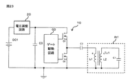
- FIG. 23 shows, as an example, a configuration in which voltage adjustment circuit 20 is inserted in the configuration of the magnetic field generation circuit of the third embodiment (FIG. 5).
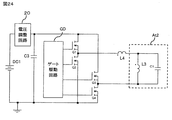
- FIG. 24 shows, as an example, a configuration in which voltage adjustment circuit 20 is inserted in the configuration of the magnetic field generation circuit of the eighth embodiment (FIG. 21).
- the coil resonance current is approximately proportional to the input voltage to the antenna regardless of the degree of deviation between the drive frequency and the resonance frequency due to the characteristics of parallel resonance. To do. Further, in the driving method using the bridge circuit as in the third to ninth embodiments, the coil resonance current is supplied to the bridge circuit or the like regardless of the degree of deviation between the driving frequency and the parallel resonance frequency of the parallel resonance circuit. It is almost proportional to the input voltage (see FIG. 10). Therefore, the parallel resonance current, that is, the spatial magnetic field strength can be adjusted by adjusting the input voltage to the bridge circuit or the like by the voltage adjustment circuit 20 as in the present embodiment.
- the output voltage of the voltage adjustment circuit 20 and the spatial magnetic field strength are almost proportional. Therefore, the correlation between the output voltage of the voltage adjustment circuit 20 and the spatial magnetic field strength may be grasped in advance, and the output voltage of the voltage adjustment circuit 20 may be set to a desired value.
- the spatial magnetic field strength can be freely adjusted without detecting the coil current or the spatial magnetic field and performing feedback control. That is, since it is possible to generate a desired spatial magnetic field strength without performing detection and feedback of the coil current and the spatial magnetic field strength, it is effective in simplifying the system and reducing the cost.
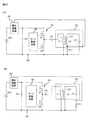
- a current monitoring resistor R11 may be connected to the secondary coil L2 of the transformer antenna At1.
- the coil current is measured by monitoring the voltage across the current monitoring resistor R11, and the measured value is fed back to the voltage adjustment circuit 20.
- the voltage adjustment circuit 20 controls the input voltage to the drive circuit (half bridge circuit 10 in the example of FIG. 25A) based on the resonance current flowing through the secondary coil L2 of the transformer antenna At1. This enables more accurate coil current control.
- a current monitoring resistor R11 may be connected in series to the resonance capacitor C1 of the transformer antenna At1. Even in this case, an effect equivalent to that obtained when the current monitoring resistor R11 is connected in series to the secondary coil L2 of the transformer antenna At1 (FIG. 25A) can be obtained.
- a current monitoring resistor R11 may be connected in series to the coil L3 of the parallel resonance coil antenna At2. Even in this case, the same effect can be obtained.
- the current monitoring resistor R11 may be disposed in the transformer antenna At1 or the parallel resonance coil antenna At2, or may be disposed outside the antennas At1 and At2.
- the values of input current and resonance current are different.
- the resonance current can be measured by measuring the voltage across the current monitoring resistor R11 connected in series to the secondary coil L2 of the transformer antenna At1 or the parallel resonance coil antenna At2 or the resonance capacitor C1.
- the current monitoring resistor R11 for example, a resistor having a resistance value that does not prevent the generation of loss in the output of the resonance current and the generated voltage has a value suitable for measurement is used.
- Embodiment 12 In the configurations of Embodiments 3 to 11, in a configuration using a half bridge circuit, a full bridge circuit, or a double forward circuit as the drive circuit, control is performed so that the switch element in the drive circuit is short-circuited after the magnetic field generation operation is completed. May be.
- the switch element Q2 is short-circuited by the gate drive circuit GD after the magnetic field generation operation is completed.
- the switch element Q1 is short-circuited by the gate drive circuit GD after the magnetic field generation operation is completed.
- the switch elements Q2 and Q4 are short-circuited by the gate drive circuit GD after the magnetic field generation operation is completed.
- the switch element Q2 is short-circuited by the gate drive circuit GD after the magnetic field generation operation is completed.
- the problem with parallel resonant circuits is that the fall time of the resonant current is long.
- the operation of the drive circuit is stopped, that is, when all the switch elements are electrically opened, the primary coil end of the transformer antenna At1 or the step-up transformer Tx2 is opened.
- the resonance current is attenuated only by the resistance loss of the resonance system.
- the time constant of 100 ⁇ s or less required by the LF communication system cannot be satisfied.
- the resonance current of the secondary coil L2 of the transformer antenna At1 and the resonance current of the parallel resonance coil antenna At2 are passed through the transformer antenna At1 and the step-up transformer Tx2. Short circuit discharge can be performed on the primary side. As a result, the resonance current is quickly attenuated, and the fall time of the magnetic field strength is shortened.
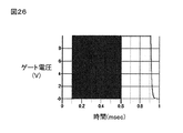
- FIG. 26 shows gate signal waveforms of the switch elements Q2 and Q4 in the simulation. After the magnetic field generation operation is stopped (after the gate signal to the switch elements Q1 and Q2 is turned off), an ON signal is input only to the gate of the switch element Q2 and the gate of the switch element Q4, and the switch elements Q2 and Q4 are electrically short-circuited. I am letting.
- the switch elements Q2 and Q4 are normally turned on during a period from 0.1 ms to 0.6 ms, and the switch elements Q2 and Q4 are discharged during a period from 0.6 ms to 0.9 ms (Q2 , Only Q4 is on). Note that the switch elements Q2 and Q4 may be turned on for a period after 0.9 ms elapses until the next operation starts. That is, the switch elements Q2 and Q4 may be turned on during the period from 0.6 ms to 0.9 ms, and thereafter, the switch elements Q2 and Q4 may be turned on or off.
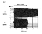
- FIG. 27 shows a simulation result of the resonance current of the secondary coil L2 of the transformer antenna At1.
- FIG. 27A shows a case where there is no short circuit operation of the switch element
- FIG. 27B shows a case where there is a short circuit operation of the switch element.
- FIG. 27A when there is no short circuit operation, the resonance of the coil current continues even after 0.6 ms, which is the end of the magnetic field generation operation.
- FIG. 27B it can be seen that when the short-circuit operation is performed, the resonance current is rapidly attenuated after the magnetic field generation operation is completed.
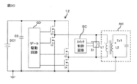
- FIG. 28 to FIG. 31 show configuration examples when the idea of the present embodiment is applied to a magnetic field generation circuit including a transformer antenna At1.
- the switch can be composed of, for example, an FET or a relay.
- the switch S1 is connected in parallel to the primary coil L1 of the transformer antenna At1 in the configuration shown in FIG. Further, in the configuration shown in FIG. 28, a switch control circuit SC for controlling on / off of the switch S1 is provided.
- the switch control circuit SC turns on the switch S1 after the magnetic field generating operation of the magnetic field generating circuit is completed. Thereby, the primary coil L1 is short-circuited and the resonant current flowing through the primary coil L1 can be forcibly discharged.
- the configuration shown in FIG. 29 is the same as the configuration shown in FIG. 15 having a full bridge circuit as a drive circuit, but between the high voltage side end of the primary coil L1 of the transformer antenna At1 and the ground potential (low voltage side output end of the DC power supply DC1). Is connected to the switch S1.
- a switch S2 is connected between the low voltage side end of the primary coil L1 of the transformer antenna At1 and the ground potential point.
- a switch control circuit SC for controlling on / off of the switches S1 and S2 is provided. The switch control circuit SC turns on the switches S1 and S2 after completion of the magnetic field generation operation of the magnetic field generation circuit. Thereby, the primary coil L1 is short-circuited and the resonant current flowing through the primary coil L1 can be forcibly discharged.
- FIG. 30 is the same as the configuration shown in FIG. 15 provided with a full bridge circuit as a drive circuit, but a switch S1 is connected in parallel to the primary coil L1 of the transformer antenna At1. Further, a switch control circuit SC for controlling on / off of the switch S1 is provided. The switch control circuit SC turns on the switch S1 after the magnetic field generating operation of the magnetic field generating circuit is completed. Thereby, the primary coil L1 is short-circuited and the resonant current flowing through the primary coil L1 can be forcibly discharged.
- the configuration shown in FIG. 31 is the same as the configuration shown in FIG. 18 having a double forward circuit as a drive circuit, but between the low voltage side end of the primary coil L1 of the transformer antenna At1 and the ground potential (low voltage side output end of the DC power supply DC1). Is connected to the switch S1. Further, a switch control circuit SC for controlling on / off of the switch S1 is provided. The switch control circuit SC turns on the switch S1 after the magnetic field generating operation of the magnetic field generating circuit is completed. Thereby, the low voltage side end of the primary coil L1 is connected to the ground, and a current path of the diode D1, the primary coil L1, and the switch S1 is formed, and the resonance current can be forcibly discharged in this path.
- the resonance current remaining in the transformer antenna At1 (or the parallel resonance coil antenna At2) can be forcibly discharged by short-circuiting the switches S1 and S2 after the magnetic field generation operation is completed, and the resonance current rises.
- the fall time can be greatly shortened.
- a diode D1 may be connected in parallel to the bypass capacitor C2.
- the cathode of the diode D1 is connected to the connection point between the switching elements Q1 and Q2 of the half-bridge circuit, and the anode of the diode D1 is connected to the high-voltage side end of the primary coil L1 of the transformer antenna At1.
- the switch element Q2 is short-circuited in order to discharge the resonance current after the magnetic field generation period ends as described in the twelfth embodiment.
- the half bridge circuit 10 when used as a drive circuit, a bypass capacitor C2 connected in series to the half bridge circuit 10 and the antenna At1 is required.
- the bypass capacitor C2 accumulates electric charges as the half bridge circuit 10 operates. Therefore, when the diode D1 as described above is not provided, even if the switch element Q2 is electrically shorted to discharge the resonance current after the end of the magnetic field generation period, the charge charged in the bypass capacitor C2 In some cases, a DC resonance phenomenon occurs between the bypass capacitor C2 and the primary coil L1, and the resonance current does not decay quickly. In the present embodiment, this problem is solved by providing the diode D1.
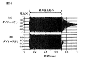
- FIG. 33 shows simulation results for changes in the resonance current when the short-circuit control shown in the twelfth embodiment is performed in each of the configuration shown in FIG. 5 (without the diode D1) and the configuration shown in FIG. 32 (with the diode D1).
- Shown in FIG. 33A shows a simulation result when the short-circuit control shown in the twelfth embodiment is performed in the configuration shown in FIG. 5 that does not have the diode D1 connected in parallel to the bypass capacitor C2.
- FIG. 33B shows a simulation result when the short-circuit control shown in the twelfth embodiment is performed in the configuration shown in FIG. 32 in which the diode D1 is connected in parallel to the bypass capacitor C2.
- FIG. 33A and 33B show simulation results of the resonance current of the secondary coil L2 of the transformer antenna At1.
- the normal on operation is performed for a period from 0.1 ms to 0.6 ms, and the discharge operation (only the switch element Q2 is turned on) for a period from 0.6 ms to 1.0 ms.
- FIG. 33A when the diode D1 is not connected in parallel to the bypass capacitor C2, the degree of attenuation is small after 0.6 ms at the end of the magnetic field generation operation, and the resonance current disappears only after 400 ⁇ s. Yes.
- FIG. 33B it can be seen that when the diode D1 is connected in parallel to the bypass capacitor C2, the resonance current is rapidly attenuated in a short period of about 40 ⁇ s.
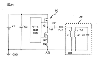
- FIG. 34 shows a configuration in which a discharge resistor R21 is added to the magnetic field generating circuit including the half bridge circuit 10 and the transformer antenna At1 shown in FIG.
- the discharge resistor R21 includes a connection point (point A) of the switch element Q2 on the low voltage side and a ground node GND for providing a ground potential, a connection point (point B) of the switch elements Q1 and Q2, and the primary coil L1 of the transformer antenna At1. It is inserted on a path connecting the connection point (point C) of the ground node GND.
- only one discharge resistor R21 is inserted, but two or more discharge resistors may be inserted.
- the current flowing through the half bridge circuit 10 is very small, and the loss in the discharge resistor R21 is also small.
- the switch element Q1 is opened, and the switch element Q2 is short-circuited, the number of turns of the secondary resonance current in the above path (path connecting point A, point B, and point C) A current that is twice as large flows. Therefore, even if the value of the discharge resistor R21 is small, it is possible to discharge quickly, and the resonance current of the secondary coil L2 of the transformer antenna At1 can be quickly attenuated.
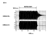
- FIG. 35 shows a simulation result of the resonance current flowing in the secondary coil L2 with and without the discharge resistor R21 in the circuit configuration of FIG.
- the resonance current was quickly attenuated after the end of the magnetic field generation period even though there was almost no difference in the waveform.
- FIG. 36 shows a configuration in which discharge resistors R21 to R23 are added to the magnetic field generating circuit including the full bridge circuit 12 and the transformer antenna At1 shown in FIG.
- the discharge resistors R21 to R23 include a connection point (point A) between the switch element Q2 and the ground node GND, a connection point (point B) between the switch element Q1 and the switch element Q2, and a connection point between the switch element Q3 and the switch element Q4 ( C point) and a current path connecting the switching element Q4 and the connection point (D point) of the ground node GND.
- at least one discharge resistor may be inserted on the above-described current path.
- FIG. 37 shows the simulation results of the resonance current of the secondary coil L2 with and without the discharge resistors R21 to R23 in the circuit configuration of FIG. In the full bridge circuit 12 as well, it can be seen that the resonance current attenuates promptly after the end of the magnetic field generation period, although there is almost no difference in the waveform at the time of resonance.
- FIG. 39 shows a magnetic field generation circuit in which a discharge resistor R21 is inserted in series with the resonance current discharge switch S1 in the circuit shown in FIG.
- FIG. 39 is the same as the configuration in which the switch S1 and the discharge resistor R21 are inserted into the half-bridge circuit 10 shown in FIG. Even in such a circuit, the same effects as those of the circuit configuration shown in FIG. 34, FIG. 36 or FIG. 38 can be obtained.
- a discharge resistor may be inserted similarly.
- the first magnetic field generating circuit is A transformer antenna including a transformer (Tx1) including a primary coil (L1) and a secondary coil (L2), and a resonant capacitor (C1) connected in parallel to the secondary coil (L2) of the transformer, and generating a magnetic field.
- Tx1 transformer
- L1 primary coil
- L2 secondary coil
- C1 resonant capacitor
- At1 AC power supply circuits (AC1, DC1 + 10, 12, 14, 16) for supplying an AC voltage as a drive voltage to the primary coil (L1) of the transformer antenna (At1).
- the resonance frequency of the parallel resonance circuit composed of the secondary coil (L2) and the resonance capacitor (C1) is set equal to the frequency of the AC voltage supplied from the AC power supply circuit (AC1).
- the AC power supply circuit may be a circuit (AC1) that outputs a sinusoidal AC voltage.
- the AC power supply circuit includes a DC power supply (DC1) that outputs a DC voltage, and a drive circuit that converts the DC voltage into a rectangular-wave AC voltage having a predetermined frequency and outputs it ( 10, 12, 14, 16) (see FIGS. 5, 12 to 14, 15, 18, 19).
- DC1 DC power supply
- drive circuit that converts the DC voltage into a rectangular-wave AC voltage having a predetermined frequency and outputs it ( 10, 12, 14, 16) (see FIGS. 5, 12 to 14, 15, 18, 19).
- the drive circuit is, for example, a half bridge circuit (10), a full bridge circuit (12), a double forward circuit (14), or a push-pull circuit (16) (FIG. 5).
- the drive circuit includes a high voltage side switch element and a low voltage side switch connected in series between the high voltage side output terminal and the low voltage side output terminal of the DC power supply (DC1).
- a half-bridge circuit (10) including the elements (Q1, Q2) and a bypass capacitor (C2) inserted between the high-voltage side and / or low-voltage side switching element and the primary coil (L1) may be used.
- a diode (D1) is further connected in parallel to the bypass capacitor (C2) so that the cathode is connected to the switch element on the high voltage side and / or the low voltage side, and the anode is connected to the primary coil (L1).
- the drive circuit may be driven within an on-duty ratio range of 10% to 45% (see FIGS. 15, 18, and 19).
- a voltage adjustment circuit (20) that receives a DC voltage from the DC power supply (DC1) and adjusts the DC voltage output to the drive circuit is further provided. You may provide (refer Embodiment 10).
- the magnetic field generation circuit of (7) may further include a current detection resistor (R11) for detecting a resonance current flowing through the secondary coil.
- the voltage adjustment circuit (20) may control the DC voltage output to the drive circuit based on the value detected by the current detection resistor (see Embodiment 11).
- the drive circuit (10, 12, 14, 16) is connected in series between the high-voltage side output terminal and the low-voltage side output terminal of the DC power supply.
- the high voltage side switch element and the low voltage side switch element (Q1, Q2,7) Connected to each other and a gate drive circuit (GD) for driving the high voltage side and low voltage side switch elements may be provided.
- the gate drive circuit (GD) may turn on either the high-voltage side or the low-voltage side switch element after the magnetic field generation operation by the drive circuit (10, 12, 14, 16) is finished (the embodiment). 12).
- a ground node for applying a ground potential
- switch elements Q2, Q4 having one end connected to the ground node
- the discharge resistors R21, R22, R23
- the second magnetic field generating circuit is A step-up transformer (Tx2) including a primary coil (L1) and a secondary coil (L2); A parallel resonant coil antenna (At2) that includes a third coil (L3) and a resonant capacitor (C1) connected in parallel to the third coil (L3); An AC power supply circuit (AC1) that supplies an AC voltage as a drive voltage to the step-up transformer (Tx2).
- the resonance frequency of the resonance circuit composed of the secondary coil (L2) and the parallel resonance coil antenna (At2) is set equal to the frequency of the AC voltage supplied from the AC power supply circuit (AC1).
- the AC power supply circuit (AC1) may be a circuit that outputs a sinusoidal AC voltage (see Embodiment 2).
- the third magnetic field generating circuit is A first coil (L4, L1); A parallel resonant coil antenna (At2, At3) that includes a second coil (L3, L2) and a resonant capacitor (C1) connected in parallel to the second coil (L3, L2); An AC power supply circuit that supplies a rectangular wave AC voltage as a drive voltage to the parallel resonant coil antennas (At2, At3).
- the resonant frequency of the parallel resonant coil antenna (At2, At3) is set equal to the frequency of the AC voltage supplied from the AC power supply circuit.
- the first coil and the second coil may be formed on the outer periphery of the same closed magnetic circuit core.
- the AC power supply circuit converts the DC voltage into a rectangular wave AC voltage of a predetermined frequency and outputs the DC voltage (DC1) that outputs a DC voltage.
- the drive circuit may be a half bridge circuit (10), a full bridge circuit (12), a double forward circuit (14), or a push-pull circuit (16).
- the drive circuit may be driven within an on-duty ratio range of 10% to 45%.
- the first to fifteenth embodiments have been described above as specific examples of the present invention.
- the present invention is not limited to the above-described embodiment, and can also be applied to an embodiment in which changes, replacements, additions, omissions, etc. are made as appropriate.
- the constituent elements described in the first to fifteenth embodiments can be combined with each other to form a new embodiment. That is, the above-described embodiment is for illustrating the technique in the present invention, and various modifications, replacements, additions, omissions, etc. can be made within the scope of the claims or an equivalent scope thereof.
Landscapes
- Inverter Devices (AREA)
Abstract
磁界発生回路は、一次コイル(L1)と二次コイル(L2)を含むトランス(Tx1)と、前記トランスの二次コイル(L2)に並列に接続された共振コンデンサ(C1)とを含み、磁界を発生するトランスアンテナ(At1)と、トランスアンテナ(At1)の一次コイル(L1)に駆動電圧として交流電圧を供給する交流電源回路(AC1,DC1,10,12,14,16)と、を備える。二次コイル(L2)と共振コンデンサ(C1)で構成される並列共振回路の共振周波数が、交流電源回路(AC1)から供給される交流電圧の周波数と等しく設定される。
Description
本発明は、通信のための磁界を発生する磁界発生回路に関する。
自動車等のドアの解錠、施錠を遠隔操作で行うためにキーレスエントリシステムとよばれる通信システムが普及している。また近年では、リモコンが車両に近づくだけで自動的に解錠し、また離れるだけで自動的に施錠されるVLF帯やLF帯の磁界信号を使用したパッシブエントリーシステムあるいはスマートエントリシステムと呼ばれる近距離通信システムが普及している。
パッシブキーレスエントリシステムの構成例として、例えば特許文献1に示されるように、車両側からはVLF帯やLF帯の磁界信号を発信し、これを受信したリモコンから高周波(RF帯)の電波信号を送信し、高周波信号を受信した車両で解錠・施錠を行う構成がある。
磁界信号の送信回路において、通信システムの信号周波数と直列共振周波数が等しくなるような定数を持つインダクタ(コイル)とコンデンサが直列に接続されたコイルアンテナが使用される。図40にそのような磁界信号の送信回路の例を示す。図40に示すような回路において、コイルアンテナに抵抗R1を介して交流電源AC0を接続し、共振周波数と等しい交流電圧V1が印加されると、低電圧でも大きなコイル電流を流すことが可能となり、大きな磁界出力を得ることができる。このようなコイルアンテナと駆動方式の組み合わせは磁界を利用した近距離通信システムに特に適したものとなり、ほぼ全てのパッシブキーレスエントリシステムに採用されている。
直列共振回路の特性として、共振電流が共振周波数をピークとした周波数特性をもつことと、電流値が極大値に達するまでに時間を要することがある。
直列共振回路は共振周波数で電流が極大ピークとなる周波数特性を持つ(一般に共振回路の周波数急峻特性はQ値であらわされる)。部品バラツキ等により製品の共振周波数を駆動周波数に完全に合わせることは難しく、このままでは製品の小さな特性バラツキが共振電流の大きな差異となってしまい使用が難しくなる。そこで、LC回路に直列に抵抗R1(以下「ダンピング抵抗」と呼ぶ)を接続している(図40参照)。これにより前述のQ値が下がって周波数電流特性をフラットにして使い勝手を上げている。
直列共振回路中のダンピング抵抗R1の抵抗値をR1、コイルL1’のインダクタンスをL1’とすると、共振電流が極大値に増加するまでの時間(以下「立ち上り時間」と呼ぶ)は、おおよそL1’/R1に比例する。パッシブキーレスエントリシステムにおいて、この立ち上り時間は通信速度を決める重要な要素となる。上述のダンピング抵抗を接続することにより、立ち上り時間を短縮することができる。ダンピング抵抗の値はシステムが要求する共振電流の周波数特性や立ち上り時間、LやCの特性値から総合的に決定される。
図40の回路でC1=10nF、L1=162μHと設定した場合に、R1をそれぞれ1Ωと10Ωにした場合の入力電流の周波数特性を図41に、電流過渡特性を図42に示す。図41より、ダンピング抵抗R1が1Ωにおいては入力電流の周波数特性が非常にピーキーとなっていることが分かる。実使用においてLC回路の特性バラツキによる電流値の変化を駆動回路にて調整することは非常に困難であり、ダンピング抵抗による制限にて電流値を安定させている。
図42より、ダンピング抵抗R1が1Ωでは、入力電流(共振電流)の立ち上りに1s以上かかっているが、ダンピング抵抗R1を10Ωとすることにより、その立ち上りが10μsに改善されていることが分かる。
以上より、ダンピング抵抗はVLF帯やLF帯の磁界通信システムに使用されるコイルアンテナ駆動方式において必須の部品で有ることが確認できる。
従来のパッシブキーレスエントリシステムにおいて、車両-リモコンキー間の通信距離が1m程度で使用されてきたが、近年ではより遠い距離、例えば通信距離を10m程度まで延長した用途が要求されるようになってきた。例えば、リモコン保持者が近付いてきたら車両の位置をランプの点滅で知らせるウェルカムライト機能、10m程度離れると自動的に施錠するウォークアウェイロック、所有者が10m程度の近距離にいることが確認できた時のみに動作する自動運転駐車機能、等がある。
これらを実現するためには、車両側の磁界信号を大幅に増加させる必要がある。一般に直列共振回路を含むアンテナシステムにおいて磁界出力(すなわち、空間磁束密度)を増加させるためには、下記の手法が考えられる。
1)コイル電流値を増加する(空間磁界強度は電流値にほぼ比例)。
2)コイルインダクタンスを増加する(空間磁界強度はインダクタンス比の平方根にほぼ比例)。
3)コイルのコアを長くする(空間磁界強度はコイルのコアの長さにほぼ比例)。
1)コイル電流値を増加する(空間磁界強度は電流値にほぼ比例)。
2)コイルインダクタンスを増加する(空間磁界強度はインダクタンス比の平方根にほぼ比例)。
3)コイルのコアを長くする(空間磁界強度はコイルのコアの長さにほぼ比例)。
コイル電流を増加させるためには、前述のダンピング抵抗を小さくするか、入力電圧を上げる必要があるが、電流値の共振特性や立ち上り時間短縮のためにダンピング抵抗値を小さくすることができず、また入力電圧値は車両のシステム電圧から決定され通常は簡単に上げることができない。仮に電圧を上げることができたとしても、ダンピング抵抗での損失が電流値の2乗で増加するためにダンピング抵抗の電流容量のアップが必要となってくる。
コイルのインダクタンスを増加させた場合、電流立ち上り時間が大きくなるためにダンピング抵抗値を増加させて立ち上り時間を同程度に保つ必要があるが、この場合、電流値が減少してしまうため、結果として、磁界強度を増加させることができない。
以上の点から、従来、3)のコイルのコアを長くすることにより磁束密度のアップを図る方法が一般的である。1m程度の通信の場合は40~80mmの長さのコアでシステムが要求する磁界発生が可能であったが、10mの中距離通信では200mm超の長さのコアが必要となる。このため、コストの上昇/生産性の低下/部品設置スペースの増加/製品信頼性の低下など、様々な課題が生じる。
直流共振現象は、共振の程度、すなわち回路がもつ共振周波数とQ値及び駆動周波数の相間関係により共振電流の強度が決まる。そのため空間に発生する磁界を制御するためにはコイルに流れる電流を検知し、回路の出力電圧などを調整する、いわゆる電流制御回路を構成する必要がある。そのため回路の構成が複雑になりコストが増大することがある。このように、直列共振現象を利用したアンテナシステムにおいては上述のような問題がある。
本発明は、例えばキーレスエントリシステムにおける通信装置に好適な、磁界を発生する磁界発生回路を提供する。
本発明の第1の態様の磁界発生回路は、磁界を発生するトランスアンテナと、トランスアンテナの一次コイルに駆動電圧として交流電圧を供給する交流電源回路と、を備える。トランスアンテナは、一次コイルと二次コイルとを含むトランスと、トランスの二次コイルに並列に接続された共振コンデンサとを含む。二次コイルと共振コンデンサで構成される並列共振回路の共振周波数が、交流電源回路から供給される交流電圧の周波数と等しく設定される。
本発明の第2の態様の磁界発生回路は、一次コイルと二次コイルを含む昇圧トランスと、磁界を発生する並列共振コイルアンテナと、昇圧トランスに駆動電圧として交流電圧を供給する交流電源回路と、を備える。並列共振コイルアンテナは、第3のコイルと、第3のコイルに並列接続された共振コンデンサとを含む。二次コイルと並列共振コイルアンテナで構成される共振回路の共振周波数が、交流電源回路から供給される交流電圧の周波数と等しく設定される。
本発明の第3の態様の磁界発生回路は、第1のコイルと、磁界を発生する並列共振コイルアンテナと、並列共振コイルアンテナに駆動電圧として矩形波交流電圧を供給する交流電源回路と、を備える。並列共振コイルアンテナは、第2のコイルと、第2のコイルに並列接続された共振コンデンサとを含む。並列共振コイルアンテナの共振周波数が、交流電源回路から供給される交流電圧の周波数と等しく設定される。
本発明によれば、並列共振回路を用いて磁界を発生させる回路を構成でき、これにより直列共振回路に起因する問題を解決できる。
以下、添付の図面を参照しながら、本発明に係る磁界発生回路の実施の形態を具体的に説明する。
(並列共振現象を用いる際の課題)
従来、空間磁界を発生させるためのアンテナとして、一般的には、コイルとコンデンサを直列に接続し、直列共振現象を利用したコイルアンテナが使用されていた。しかし、直列共振現象を利用したコイルアンテナには、前述のとおり、高出力を得るためには回路の複雑化、高出力化が必要になりコストが増大する等の問題があった。
従来、空間磁界を発生させるためのアンテナとして、一般的には、コイルとコンデンサを直列に接続し、直列共振現象を利用したコイルアンテナが使用されていた。しかし、直列共振現象を利用したコイルアンテナには、前述のとおり、高出力を得るためには回路の複雑化、高出力化が必要になりコストが増大する等の問題があった。
そこで、直列共振現象に代えて並列共振現象を利用することが考えられる。しかし、従来、並列共振現象を用いた磁界装置はほとんど実現されていなかった。その理由について下記に説明する。
図43に基本的な並列共振回路を示す。並列共振回路は、開磁路コアにコイルが巻回されて構成されたコイルL1’と、コンデンサC1’とが並列に交流電源ACに接続されている。並列共振において、入力電圧がV、共振周波数がfLの場合、I=V/(2πfL)となる共振電流Iが流れる。例えば、コイルL1’のインダクタンスが165μH、駆動周波数fが125kHの場合に、共振電流Iが1アンペアの仕様要求があったときは、これを満たすためには駆動電圧として、130V(ピークからピークまでの値)の正弦波電圧を印加する必要がある。しかし、車載システムにおいて、このような高電圧の駆動系を実現するのは非常に難しい。
また並列共振を生じさせるためには正弦波電圧を印加する必要があるが、一般に用いられるブリッジ回路等による矩形波電圧を印加しても、高次成分を持つ矩形波電圧ではLC並列共振を発生させることはできない。また、LF帯の正弦波電圧を生成するのは困難かつコストもかかる。例えば、図44、図45に、インダクタンスが165μHのコイルL1’と、容量が10μFのコンデンサC1’との並列共振回路に対して、正弦波電圧と矩形波電圧を印加した場合のシミュレーション波形を示す。図44は、その並列共振回路に125kHz、130V(ピークからピークまでの値)の正弦波電圧を印加した場合の、入力電流に流れるコイル電流の波形(図30(B))、及びコイルL1’に流れるコイル電流の波形(図30(A))をそれぞれ示した図である。図45は、その並列共振回路に対して、125kHz、130V(ピークからピークまでの値)の矩形波電圧を印加した時の入力電流及びコイル電流の波形をそれぞれ示す。図44を参照すると、正弦波電圧印加時は、共振によるコイル電流が発生していることがわかる。これに対して、図45(A)、(B)を参照すると、矩形波電圧印加時は、入力電流において60Aのピーク電流が発生しているが、そのピーク電流を除き、入力電流とコイル電流はほぼ同じ値となっており、矩形波電圧では並列共振が発生していないことが分かる。
以上の点が主な原因として、磁界発生回路において、従来、並列共振回路が適用されなかったと考えられる。
以下の各実施の形態において、従来では困難であった並列共振現象を用いて磁界を発生させることを可能とする磁界発生回路(磁界通信回路)の構成を説明する。このような磁界発生回路は、例えば、自動車のキーレスエントリシステムに適用されるVLF帯やLF帯の磁界信号を発生する通信装置に有用である。
(実施の形態1)
図1は、本発明の実施の形態1における磁界発生回路の構成を示した図である。
図1は、本発明の実施の形態1における磁界発生回路の構成を示した図である。
実施の形態1における磁界発生回路は、正弦波交流電圧を発生させる交流電源回路AC1と、一次コイルL1と二次コイルL2を含むトランスTx1と、トランスTx1の二次コイルL2と共振回路を構成する共振コンデンサC1とを備える。
トランスTx1は、図2に示すように、開磁路コアCo(棒状コア)の外周に一次コイルL1と二次コイルL2を巻回して構成される。トランスTx1の二次コイルL2には、共振コンデンサC1が並列に接続される。トランスTx1の二次コイルL2と共振コンデンサC1は並列共振回路を構成する。その並列共振回路の共振周波数は、交流電源回路AC1による駆動周波数と等しくなるように設定される。このため、二次コイルL2のインダクタンス(L2)とコンデンサC1の容量(C1)はそれぞれ、共振周波数が駆動周波数と等しくなるような値に設定される。さらに、一次コイルL1への入力電圧に対して所望の二次コイルL2の出力電圧が得られるように、一次コイルL1と二次コイルL2の巻数の比が設定されている。トランスTx1と共振コンデンサC1は、トランス構造をもつ磁界発生用アンテナとして機能する。以下、トランスTx1と共振コンデンサC1により構成されるアンテナを「トランスアンテナ」At1と呼ぶ。なお、二次コイルL2と共振コンデンサC1で構成される並列共振回路の共振周波数と、交流電源回路AC1から供給される交流電圧の周波数である駆動周波数とは、必ずしも厳密に等しくなるような値に設定する必要はなく、たとえば±10%の範囲で等しくなるような値に設定すればよい。
トランスアンテナAt1の一次コイルL1に、正弦波電圧を供給する交流電源回路AC1が接続される。交流電源回路AC1は、所定の駆動周波数の正弦波電圧を、トランスアンテナAt1の一次コイルL1に印加する。これにより、トランスアンテナAt1は、二次コイルL2に正弦波電流を発生させ、交流磁界を発生させる。このように、交流電源回路AC1はトランスアンテナAt1の駆動回路として機能する。
トランスアンテナAt1の二次コイルL2のインダクタンスの値と、共振電流Iの設定値とは、要求される空間磁束密度に基づき算出される。具体的には、共振電流I=V/(2πfL)の関係に基づき、必要な電圧値Vを算出し、入力電圧、一次・二次結合度、二次コイルL2のインダクタンスから、巻数比及び/または一次コイルL1のインダクタンス値を算出する。強い空間磁束強度が要求される場合、大きな二次コイルL2のインダクタンス及び大きな共振電流Iが必要となるため、一次巻数を極小(1~数回)とする必要があり、一次コイルL1と二次コイルL2を配置する位置が非常に重要となってくる。
上記の構成を有する本実施の形態の磁界発生回路は、並列共振現象を利用していることから、コイル電流の立ち上がり時間が短く、共振電流値の周波数によるバラツキが少ない。また、直列共振回路で必要であったダンピング抵抗が不要となる。このため、ダンピング抵抗での損失が無くなり、回路の効率が改善される。また、ダンピング抵抗や電流立ち上がり時間といった制約が無くなるため、コイル電流の上限は電力や損失に関する制限のみとなる。
また、トランスTx1の巻数比とインダクタンス値を適切な値に設定することにより、二次コイルL2の出力電圧と共振電流を最適な値にすることが可能となる。例えば、共振コンデンサやコイル自身の耐電圧性を考慮して最も適したコイル-コンデンサ電圧にて動作させることが可能となる。
また、開磁路コアCoの長さを長くすることなく、コイル電流の増加により磁界出力を増加することが可能となる。同様に従来方式と同等出力を確保しつつ、開磁路コアCoの長さを短くすること、すなわち、小型化が可能となる。
また、並列共振周波数と駆動周波数にずれが生じても、磁界を発生させる二次コイル共振電流変化はほとんど生じない。
図3に、従来の磁界発生回路(図34)と本実施の形態の磁界発生回路(図1)それぞれによる各種想定項目に対する実測値の比較を示す。従来の磁界発生回路では、図34に示す回路構成において、R1=10Ω、C1=10nF、L1=166μH、コアの長さ90mmのコイルアンテナとした。実施の形態1では、図1に示す回路構成において、C1=10nF、L2=166μH、二次コイル/一次コイルの巻数比N2/N1=35、開磁路コアCoの長さ90mmとした。測定データは各アンテナの共振周波数における値である。
図3を参照すると、本実施の形態では、入力電流で従来比21%、空間磁束密度で従来比172%となり、効率、出力共に大幅に改善されていることが分かる。また、並列共振では、コイル共振電流は一定で、入力電流のみがLC並列共振の程度に合わせて減少する、という基本特性があり、入力電流にバラつきは発生するものの共振の程度にかかわらず空間磁束密度を一定に保つことが容易である。
以上のように本実施の形態の磁界発生回路は並列共振現象を用いる。並列共振現象を用いる効果として、定出力化、高速化、ダンピング抵抗の削除による高効率化及びハイパワー化が可能となった点が上げられる。並列共振では、コイル共振電流が一定で、入力電流のみが並列共振の程度に応じて減少するという基本特性があり、共振の程度にかかわらず空間磁束密度を一定に保つことが容易であり、直列共振回路のようなダンピング抵抗は不要となる。
さらに並列共振は本質的に共振電流の立ち上り速度が極めて短いという基本特性があり、ダンピング抵抗を用いることなく、コイル共振電流(=空間磁束密度)の立ち上り時間を短くすることができる。またコイルのインダクタンス値が増加しても立ち上り時間に大きな変化は発生しない。ダンピング抵抗が不要となることにより、従来方式で損失の多くを占めていたダンピング抵抗での損失が無くなるため、回路効率が極めて高くなる。
またダンピング抵抗による電流制限がなく、共振電流を大きくすることが可能となる。インダクタンスを増加させても立ち上り時間に大きな影響はない。よって従来方式では出来なったインダクタンス値のアップ、あるいは回路共振電流のアップにより磁界出力のハイパワー化が可能となる。
以上のように、本実施の形態の磁界発生回路によれば、並列共振を利用しているため、コイル電流の立ち上がり時間を短くでき、共振電流値の周波数によるバラツキを低減できる。また、そのためにダンピング抵抗が不要となり、ダンピング抵抗での損失を低減でき、回路の効率が改善される。また、トランスの巻数比とインダクタンス値を適切な値に設定することにより、二次コイルの出力電圧と共振電流を好適な値にすることが可能となる。例えば共振コンデンサやコイル自身の耐電圧性を考慮して好適なコイル-コンデンサ電圧にて動作させることが可能となる。また、開磁路コアCoの長さを長くすることなく、コイル電流の増加により磁界出力を増加することが可能となる。または従来方式と同等出力において小型化が可能となる。
(実施の形態2)
本発明に係る磁界発生回路の別の構成を説明する。図4は、本発明における実施の形態2における磁界発生回路の構成を示す図である。本実施の形態の磁界発生回路は、正弦波電圧を供給する交流電源回路AC1と、昇圧トランスTx2と、並列共振コイルアンテナAt2とで構成される。並列共振コイルアンテナAt2は、コイルL3と、コイルL3に並列に接続された共振コンデンサC1とを備える。コイルL3は、トランスアンテナAt1のトランスTx1におけるリーケージインダクタンス成分の機能と同等の機能を果たす。昇圧トランスTx2は、二次コイルL2が並列共振コイルアンテナAt2と並列に接続され、一次コイルL1が駆動回路である交流電源回路AC1に接続されている。昇圧トランスTx2の二次コイルL2と並列共振コイルアンテナAt2とからなる回路の並列共振周波数は、交流電源回路AC1により供給される交流電圧の周波数である駆動周波数と等しくなるように設定される。なお、昇圧トランスTx2の二次コイルL2と並列共振コイルアンテナAt2とからなる回路の並列共振周波数と、交流電源回路AC1から供給される交流電圧の駆動周波数とは、必ずしも厳密に等しくなるように設定する必要はなく、たとえば±10%の範囲で等しくなるように設定すればよい。
本発明に係る磁界発生回路の別の構成を説明する。図4は、本発明における実施の形態2における磁界発生回路の構成を示す図である。本実施の形態の磁界発生回路は、正弦波電圧を供給する交流電源回路AC1と、昇圧トランスTx2と、並列共振コイルアンテナAt2とで構成される。並列共振コイルアンテナAt2は、コイルL3と、コイルL3に並列に接続された共振コンデンサC1とを備える。コイルL3は、トランスアンテナAt1のトランスTx1におけるリーケージインダクタンス成分の機能と同等の機能を果たす。昇圧トランスTx2は、二次コイルL2が並列共振コイルアンテナAt2と並列に接続され、一次コイルL1が駆動回路である交流電源回路AC1に接続されている。昇圧トランスTx2の二次コイルL2と並列共振コイルアンテナAt2とからなる回路の並列共振周波数は、交流電源回路AC1により供給される交流電圧の周波数である駆動周波数と等しくなるように設定される。なお、昇圧トランスTx2の二次コイルL2と並列共振コイルアンテナAt2とからなる回路の並列共振周波数と、交流電源回路AC1から供給される交流電圧の駆動周波数とは、必ずしも厳密に等しくなるように設定する必要はなく、たとえば±10%の範囲で等しくなるように設定すればよい。
交流電源回路AC1から供給される交流電圧V1は、昇圧トランスTx2の一次コイルL1に印加される。昇圧トランスTx2は、一次コイルL1と二次コイルL2の巻き数比に応じて入力電圧を変換し、並列共振コイルアンテナAt2に供給し、これにより並列共振コイルアンテナAt2から交流磁界を発生させる。
以上の構成を有する本実施の形態の磁界発生回路は、実施の形態1の場合と同様の効果を奏するとともにさらに以下の効果を奏する。昇圧を専用のトランスTx2により行うため、既存のコイルアンテナの使用が可能となる。また、結合の良い閉磁路トランスにより巻数比(昇圧比)にてコイル入力電圧を調整できるため、コイル電流の調整が容易となる。また、実施の形態1では、トランスアンテナのトランス機能によって、LC並列共振回路に印加される電圧を昇圧させていた。これに対して、本実施の形態では、専用の昇圧トランスによって電圧を上昇させる上げることにより、同様の機能を実現している。その他の動作、作用については実施の形態1と同様であるため、ここでの説明は省略する。
(実施の形態3)
実施の形態1では、トランスアンテナAt1を駆動する電圧として正弦波交流電圧を印加していた。これに対して本実施の形態では、トランスアンテナAt1を駆動する電圧として矩形波交流電圧を印加する磁界発生回路の構成を説明する。
実施の形態1では、トランスアンテナAt1を駆動する電圧として正弦波交流電圧を印加していた。これに対して本実施の形態では、トランスアンテナAt1を駆動する電圧として矩形波交流電圧を印加する磁界発生回路の構成を説明する。
図5は、本発明における実施の形態3における磁界発生回路の構成を示す図である。本実施の形態における磁界発生回路は、トランスアンテナAt1と、直流電源DC1と、トランスアンテナAt1を駆動する駆動回路としてのハーフブリッジ回路10と、を備える。直流電源DC1とハーフブリッジ回路10(駆動回路)とは、矩形波交流電圧を出力する交流電源回路を構成する。ハーフブリッジ回路10は、入力コンデンサC3と、直列接続された2つのスイッチ素子Q1、Q2と、スイッチ素子Q1、Q2を制御するゲート駆動回路GDとを備える。スイッチ素子Q1、Q2は例えばFETで構成される。
トランスアンテナAt1は実施の形態1で説明したものと同様である。トランスアンテナAt1の一次コイルL1と、ハーフブリッジ回路10の出力端子とが接続される。より具体的には、トランスアンテナAt1の一次コイルL1の高圧側端子は、バイパスコンデンサC2を介してスイッチ素子Q1とQ2の接続点に接続される。
ハーフブリッジ回路10は、直流電源DC1から入力コンデンサC3を介して直流電圧を入力し、入力した直流電圧を所望の矩形波電圧に変換し、トランスアンテナAt1に供給する。具体的には、ハーフブリッジ回路10は、2つのスイッチ素子Q1,Q2を、逆相で(排他的に)、かつ、所定のオンデューティ比にて所定の周波数で駆動することにより、直流電源DC1から所定の駆動周波数の矩形波電圧を発生させ、トランスアンテナAt1の一次コイルL1に印加する。これにより、二次コイルL2に正弦波共振電流を発生させ、空間に交流磁界を発生させる。
特に、矩形波電圧による共振動作を可能とするため、ハーフブリッジ回路10の各スイッチ素子Q1,Q2のスイッチ動作において適切なオフ区間を設ける。具体的には、スイッチング素子のオンデューティ比を10%~45%の範囲内の値に設定している。好ましくは、スイッチング素子のオンデューティ比を10%~40%の範囲内の値に設定してもよい。より好ましくは、オンデューティ比を10%~20%の範囲内の値に設定してもよい。図6(A)、(B)はそれぞれ高圧側及び低圧側のスイッチ素子Q1,Q2のタイミングチャートである。例えば、図6に示すように、オフデューティ比を75%、すなわち、オンデューティ比を25%に設定する。本発明者は、このような範囲のデューティ比に設定することにより、矩形波電圧による並列共振動作が可能となることを発見した。また、本発明者は、トランスアンテナAt1の一次コイルL1と二次コイルL2間のリーケージインダクタンスを適切に設定し、活用することにより、ハーフブリッジ回路10から出力される電流ピーク値を大幅に減衰させることが可能となることを発見した。結果として高効率な正弦波共振電流の生成が可能となった。
本実施の形態の構成において、ハーフブリッジ回路のスイッチ素子のオンデューティ比を適切な値、ここでは、10%~45%に設定している。例えば、オンデューティ比を25%に設定した場合、高圧側のスイッチQ1が25%、低圧側のスイッチ素子Q2が25%で短絡(オン)されるため、残りの50%の期間、一次コイルL1は入力電源からもGNDからも電気的にフローティングした状態となる。これがトランス結合を介したトランスアンテナ二次コイルでの並列共振回路での自由振動期間となり、この自由振動期間が二次並列共振回路での並列共振の実現を可能とする。さらにトランスアンテナの一次コイルと二次コイル間に発生するリーケージインダクタンスを活用することにより、駆動回路からトランスアンテナに流入する極大のピーク電流を制限することが可能となる。
トランスアンテナにより二次共振系に高電圧の印加が可能となり、これら4つの要素(トランスアンテナによる高電圧、自由振動期間が実現出来る回路、自由振動期間の設定、適切なリーケージインダクタンス)の組み合わせにより、初めて実用的な並列共振現象を用いた空間磁界発生回路を実現することが出来た。
図7に、本実施の形態における磁界発生回路の構成に対するシミュレーション結果を示す。シミュレーションは、L2=166μH、C1=10μF、巻数比N2/N1=35、コア長90mmとしたトランスアンテナAt1のサンプル(サンプル#1)について行った。この構成において、オンデューティが25%で矩形波電圧を印加した場合のシミュレーションを行った。図8に、直流電源からハーフブリッジ回路10への入力電流(回路入力電流)Iin、トランスTx1への入力電流(以下「トランス入力電流」という)Itr、及び二次コイルL2を流れる共振電流(以下「コイル共振電流」という)Icoilに対するシミュレーション結果を示す。また、図9に、高圧側のスイッチ素子Q1と低圧側のスイッチ素子Q2のドレイン電流及びゲート信号波形のシミュレーション結果を示す。
図8を参照すると、二次コイルL2のコイル共振電流Icoilは正弦波となっているが、トランス入力電流Itrは正弦波とは異なる波形となっていることが分かる。このトランス入力電流Itrは、抵抗損失分やLC共振周波数と駆動周波数のズレ等による二次共振電流の減衰分をハーフブリッジ回路10から供給するための電流である。この電流の値は、スイッチ素子Q1、Q2から供給される電圧と二次共振電流から励磁される電圧との差で決定され、LC並列共振周波数と駆動周波数が近接する程小さな値となる。
また、図8より、トランス入力電流Itr(Aオーダー)に対して回路入力電流Iin(mAオーダー)が極めて小さくなっていることが分かる。図8の高圧側のスイッチ素子Q1のドレイン電流の多くは、入力コンデンサC3(図5参照)より供給され、そのドレイン電流の負部分は、入力コンデンサC3に回生される電流となる。さらに低圧側のスイッチ素子Q2のドレイン電流は、二次コイルのコイル共振電流Icoilから供給され、ハーフブリッジ回路からのエネルギー供給は無い。結局、本回路で使用される電流は高圧側のスイッチ素子Q1のドレイン電流の正電流分-負電流分のみであり、この結果、回路入力電流Iin=0.014Armsに対して、二次コイルのコイル共振電流Icoil=0.636Armsと計算されている。
以上、シミュレーションによる結果を説明した。次に、実際の測定結果を示す。従来のコイルアンテナと、本実施の形態のトランスアンテナに対して測定を行った。本実施の形態については、シミュレーションで使用したサンプル#1と同じ条件のサンプル(サンプル#2)に加えて、二次インダクタンス値及び巻数比をさらに増加して、より高出力としたトランスアンテナAt1のサンプル#3(L2=337μH、巻数比70、C1=4.7μF)を用意した。図10に、従来及び本実施形態のサンプル#2、#3に対する実測結果を示す。
従来方式と比較して、回路入力電流がサンプル#2では23%に、サンプル#3では42%まで減少している。これに対して、空間磁束密度は、サンプル#2で177%に、サンプル#3が286%に大幅に増加していることが確認できた。また、本実施の形態による構成によれば、磁束密度の立ち上り時間も従来のものと同等程度であることが確認できた。
また、回路入力電流とコイル共振電流の比較に関して、従来方式では、回路入力電流Iinは0.147A(実効値)であり、コイル共振電流Icoilは0.357A(実効値)である。よって、従来方式では、コイル共振電流Icoilは回路入力電流Iinの約2.4倍であった。これに対して、本実施の形態のサンプル#2においては、回路入力電流Iinは0.034A(実効値)であり、コイル共振電流Icoilは0.665A(実効値)である。よって、コイル共振電流Icoilは回路入力電流Iinの約20倍である。一方、サンプル#3では、回路入力電流Iinは0.062A(実効値)であり、コイル共振電流Icoilは0.665A(実効値)である。よって、コイル共振電流Icoilは回路入力電流Iinの約10.7倍である。このように、本実施の形態によれば、従来方式に比べて非常に高効率に動作できることが確認できた。
本実施の形態の構成によれば、並列共振の特性により、駆動周波数変動に対するコイル共振電流の変動を低減できる。また入力電流についても入力コンデンサC3への電力回生が行われることから、駆動周波数変動に対する入力電流変動も比較的少なくなる。
図11に、サンプル#2における、駆動周波数を変動させた場合の周波数特性の実測値を示す。駆動周波数を変動させた場合に、出力される磁束密度に差異がほとんど無く、出力磁束の周波数特性が極めて安定していることが確認できる。回路入力電流については、最大値/最小値で3.5倍となった。ダンピング抵抗等の抵抗成分を極力排除した共振系としては、変動が抑制されていることが確認できた。
なお、トランスアンテナAt1に対するハーフブリッジ回路の接続方法は図5に示したものに限定されず、種々の接続方法が考えられる。例えば、図12~図14に、トランスアンテナAt1に対するハーフブリッジ回路の他の接続の例を示す。図12では、バイパスコンデンサC2が一次コイルL1の低圧側端と、ハーフブリッジ回路の低圧側出力端との間に挿入されている。図13では、トランスアンテナAt1が高圧側のスイッチ素子Q1に並列に接続され、かつ、バイパスコンデンサC2が一次コイルL1の低圧側端と、スイッチ素子Q1の低圧側端との間に挿入されている。図14では、トランスアンテナAt1が高圧側のスイッチ素子Q1に並列に接続され、かつ、バイパスコンデンサC2が一次コイルL1の高圧側端と、スイッチ素子Q1の高圧側端との間に挿入されている。
以上説明した構成を有する磁界発生回路は、実施の形態1に説明した効果に加えてさらに以下の効果を奏する。すなわち、従来技術では困難であった、構成がシンプルで制御も簡素なハーフブリッジ回路による並列共振回路の駆動が可能となる。このため、システムとしての利便性の向上、及びコスト低減を図ることができる。また、トランス側からの回生電流と低圧側スイッチ素子の動作区間での自励共振動作により、駆動回路に実際に供給される電流を極めて少なくでき、効率を改善することが可能となる。また周波数バラツキによる入力電流バラツキも低減することが可能となる。結果として、高効率で入力電流の周波数バラツキによる差異の少ない回路を実現できる。
(実施の形態4)
実施の形態3では、トランスアンテナAt1を駆動する駆動回路として、ハーフブリッジ回路を用いたが、この駆動回路はハーフブリッジ回路に限定されず、他の種類の駆動回路を使用してもよい。例えば、実施の形態3で示した各構成において、ハーフブリッジ回路10をフルブリッジ回路に変更してもよい。図15に、トランスアンテナAt1に対する駆動回路としてフルブリッジ回路を適用した構成を示す。
実施の形態3では、トランスアンテナAt1を駆動する駆動回路として、ハーフブリッジ回路を用いたが、この駆動回路はハーフブリッジ回路に限定されず、他の種類の駆動回路を使用してもよい。例えば、実施の形態3で示した各構成において、ハーフブリッジ回路10をフルブリッジ回路に変更してもよい。図15に、トランスアンテナAt1に対する駆動回路としてフルブリッジ回路を適用した構成を示す。
図15に示すように、フルブリッジ回路12は、入力コンデンサC3と、4のスイッチ素子Q1~Q4と、スイッチ素子Q1~Q4を制御するゲート駆動回路GDとを備える。スイッチ素子Q1、Q2は直列に接続され、スイッチ素子Q3、Q4は直列に接続される。スイッチ素子Q1、Q2の直列回路と、スイッチ素子Q3、Q4の直列回路とは並列に接続される。トランスアンテナAt1は実施の形態1で説明したものと同様である。スイッチ素子Q1とスイッチ素子Q2の接続点は、トランスアンテナAt1の一次コイルL1の高圧側端に接続され、スイッチ素子Q3とスイッチ素子Q4の接続点は、トランスアンテナAt1の一次コイルL1の低圧側端に接続される。
フルブリッジ回路12は、直流電源DC1からの直流電圧を入力コンデンサC3を介して入力し、スイッチ素子Q1~Q4をオン・オフ駆動することで、入力した直流電圧から所望の駆動周波数の矩形波交流電圧を生成する。生成された矩形波交流電圧はトランスアンテナAt1の一次コイルL1に印加され、これにより、二次コイルL2に正弦波共振電流を発生させ、空間に交流磁界を発生させる。フルブリッジ回路12に対しても、ハーフブリッジ回路10の場合と同様に、スイッチ素子Q1、Q2およびQ3、Q4のオンデューティ比を適切な値、ここでは10%~45%に設定して駆動する。
このとき、トランスアンテナAt1の一次コイルL1には、直流電源DC1が供給する電圧(すなわち、回路入力電圧)の振幅の2倍の振幅の交流電圧が印加される。トランスアンテナAt1は“トランス”としての機能を有するため、入力電圧が2倍になれば出力電圧も2倍となる。このため、本構成により、容易にコイル電流すなわち空間磁束密度を増加させることが可能となる。トランスアンテナAt1の仕様を変えて出力電圧が変わらないように調整すると、逆にスイッチ素子Q1~Q4一個当たりの電流は約1/2となるため、スイッチ素子Q1~Q4に必要な電流値が下がり、より性能の低い仕様の(すなわち、安価な)スイッチ素子を使用することが可能となる。
図16に、直流電源DC1からゲート駆動回路GDへの回路入力電流Iin、トランス入力電流Itr、及び二次コイルL2コイル共振電流Icoilの電流波形のシミュレーション結果を示す。
図15に示す回路構成において、オンデューティ比25%の矩形波電圧を印加したときのシミュレーションを行った。図17に、そのシミュレーション結果を示す。なお、図17では、実施の形態4の回路構成によるシミュレーション結果に加えて、比較のために、実施の形態3の構成によるシミュレーション計算も合わせて示している。使用したトランスアンテナAt1の仕様は、二次コイルL2のインダクタンス値(L2)=166μH、コンデンサC1の容量(C1)=10nF、トランスTx1の巻数比N2/N1=35でコアの長さ90mmとした。駆動回路(ハーフブリッジ回路またはフルブリッジ回路)のみが異なっている。実施の形態3に対して、実施の形態4の結果では、フルブリッジ回路12への入力電流比は約340%となっている。一方、トランスアンテナAt1への入力電流比は140%にとどまっている。これはフルブリッジ回路12により各スイッチ素子Q1~Q4の電流ピーク値が減少したことを示している。また空間磁束密度比は198%となり、大きく増加していることが確認できる。以上より、トランスアンテナAt1とフルブリッジ回路12の組み合わせが、スイッチ素子Q1~Q4の電流の電流値の低減や空間磁束密度の増加に大きな効果が有ることが確認できた。
本実施の形態の構成によれば、実施の形態1及び3の構成による効果に加えてさらに以下の効果を奏する。フルブリッジ回路12を使用することにより、一次コイルL1に印加される電圧が、直流電源DC1の電圧に対して実質的に2倍となる。このことから、コイル出力電流を更に増加させることが可能となる。逆に、コイル電流出力を同等とする場合、各スイッチ素子に対する最大のドレイン電流を1/2にすることが可能となり、低い性能のスイッチ素子やICの使用が可能となり、よって、スイッチ素子等の選定が容易になる。
(実施の形態5)
実施の形態3で示した各構成において、トランスアンテナAt1に対する駆動回路として、ハーフブリッジ回路10に代えてダブルフォワード回路を使用してもよい。
実施の形態3で示した各構成において、トランスアンテナAt1に対する駆動回路として、ハーフブリッジ回路10に代えてダブルフォワード回路を使用してもよい。
図18に、トランスアンテナAt1に対する駆動回路としてダブルフォワード回路を適用した構成を示す。ダブルフォワード回路14は、入力コンデンサC3と、スイッチ素子Q1とダイオードの直列回路と、ダイオードD2とスイッチ素子Q2の直列回路と、スイッチ素子Q1、Q2を制御するゲート駆動回路GDとを備える。スイッチ素子Q1とダイオードD1の直列回路と、ダイオードD2とスイッチ素子Q2の直列回路とは並列に接続される。トランスアンテナAt1は実施の形態1で説明したものと同様である。スイッチ素子Q1とダイオードD1の接続点は、トランスアンテナAt1の一次コイルL1の高圧側端に接続される。ダイオードD2とスイッチ素子Q2の接続点は、トランスアンテナAt1の一次コイルL1の低圧側端に接続される。
ダブルフォワード回路14は、トランスアンテナAt1を駆動する場合、実施の形態3のハーフブリッジ回路10による駆動とほぼ同様の動作を行う。すなわち、ダブルフォワード回路14に対しても、スイッチ素子Q1、Q2のオンデューティ比を適切な値(ここでは10%~45%)に設定して駆動する。本実施の形態による構成によっても、実施の形態3の構成と同様の効果を奏する。
(実施の形態6)
実施の形態3で示した各構成において、トランスアンテナAt1に対する駆動回路として、ハーフブリッジ回路10に代えてプッシュプル回路を使用してもよい。
実施の形態3で示した各構成において、トランスアンテナAt1に対する駆動回路として、ハーフブリッジ回路10に代えてプッシュプル回路を使用してもよい。
図19に、トランスアンテナAt1に対する駆動回路としてプッシュプル回路16を適用した構成を示す。図19において、プッシュプル回路16は、入力コンデンサC3と、スイッチ素子Q1、Q2と、スイッチ素子Q1、Q2を制御するゲート駆動回路GDとを備える。トランスアンテナAt1のトランスTx11は、一次コイルは、第1のコイル部分L11と第2のコイル部分L12とを含む。スイッチ素子Q2は、第2のコイル部分L12の低圧側において第2のコイル部分L12と直列に接続される。スイッチ素子Q1は、一次コイルL1及びスイッチ素子Q2からなる直列回路に並列に接続される。直流電源DC1の高圧側出力端は、第1のコイル部分L11と第2のコイル部分L12の接続点に接続される。スイッチ素子Q1、Q2の低圧側端は、直流電源DC1の低圧側出力端に接続される。
このようなプッシュプル回路16に対しても、ハーフブリッジ回路10の場合と同様に、スイッチ素子Q1、Q2のオンデューティ比を適切な値(ここでは10%~45%)に設定して駆動する。このプッシュプル回路16によっても、実施の形態4のフルブリッジ回路と同様に、トランスアンテナAt1への印加電圧を回路入力電圧の実質的に2倍にすることができる。よって、コイル出力電流を増加すること、すなわち、入力電流を低減することが可能になる。また、フルブリッジ回路と比較して、半分の数(2個)のスイッチ素子で同等の機能を実現する回路動作を実現することが可能となる。プッシュプル回路16を備えた場合の装置の動作は実施の形態4のものとほぼ同様である。
(実施の形態7)
実施の形態2では、並列共振コイルアンテナAt2を正弦波交流電圧により駆動した。並列共振コイルアンテナAt2を、実施の形態3~6で開示したように矩形波交流電圧により駆動することもできる。すなわち、実施の形態3~6で示した構成において、トランスアンテナAt1を、実施の形態2で示した並列共振コイルアンテナAt2と昇圧トランスTx2により置き換えてもよい。このような構成であっても、実施の形態3~6と同様の効果を奏する。
実施の形態2では、並列共振コイルアンテナAt2を正弦波交流電圧により駆動した。並列共振コイルアンテナAt2を、実施の形態3~6で開示したように矩形波交流電圧により駆動することもできる。すなわち、実施の形態3~6で示した構成において、トランスアンテナAt1を、実施の形態2で示した並列共振コイルアンテナAt2と昇圧トランスTx2により置き換えてもよい。このような構成であっても、実施の形態3~6と同様の効果を奏する。
図20は、一例として、実施の形態3の図5に示す構成において、トランスアンテナAt1を並列共振コイルアンテナAt2と昇圧トランスTx2により置き換えた構成を示す図である。すなわち、図20では、並列共振コイルアンテナAt2をハーフブリッジ回路10で駆動する構成を示している。ハーフブリッジ回路10は実施の形態3と同様に動作させる。すなわち、2つのスイッチ素子Q1、Q2を、互いに逆相でかつオンデューティ比が10%~45%の範囲内で駆動する。これにより、実施の形態3と同様の効果を奏する。
なお、本実施の形態における昇圧トランスTx2の一次コイルL1と二次コイルL2間のリーケージインダクタンスは、実施の形態3で説明したトランスアンテナAt1の一次コイルL1と二次コイルL2間のリーケージインダクタンスと同等の作用を発揮する。
本実施の形態の構成によれば、従来のコイルアンテナにおけるコイルとコンデンサの接続を直列から並列に変更するだけで、本実施の形態の構成に適用することが可能となる。また、結合の良い閉磁路トランスにより、巻数比(昇圧比)によって、コイル入力電圧を調整できるため、コイル共振電流の調整が容易となる。
実施の形態3~6では、トランスアンテナAt1によりLC並列共振回路に高電圧を印加していた。これに対して、本実施の形態では、昇圧トランスTx2を用いることにより、LC並列共振回路に高電圧を供給することが可能となり、必要な共振電流を得ることができる。本実施の形態の磁界発生回路の駆動回路は、実施の形態2、3~6の場合と同様に動作させて、空間に交流磁界を発生させる。
(実施の形態8)
実施の形態2に開示した並列共振コイルアンテナAt2と、所定のインダクタンス値を有するコイルとを、実施の形態3~6に記載の各種駆動回路(すなわち、図5、12~15、18、19に示す駆動回路)と接続してもよい。
実施の形態2に開示した並列共振コイルアンテナAt2と、所定のインダクタンス値を有するコイルとを、実施の形態3~6に記載の各種駆動回路(すなわち、図5、12~15、18、19に示す駆動回路)と接続してもよい。
図21に、一例として、並列共振コイルアンテナAt2と、所定のインダクタンス値を有するコイルL4とを、駆動回路の一例としてフルブリッジ回路12に接続した構成を示す。並列共振コイルアンテナAt2の並列共振周波数は駆動周波数と等しくなるように設定される。フルブリッジ回路12を実施の形態3~6の場合と同様に動作させて、並列共振コイルアンテナAt2及びコイルL4に対して矩形波交流電圧を供給することにより、並列共振コイルアンテナAt2から空間に交流磁界を発生させることができる。なお、並列共振コイルアンテナAt2の並列共振周波数と、駆動周波数とは、必ずしも厳密に等しくなるように設定する必要はなく、たとえば±10%の範囲で等しくなるように設定すればよい。
なお、本実施の形態におけるコイルL4のインダクタンスは、実施の形態3で説明したトランスアンテナAt1の一次コイルL1と二次コイルL2間のリーケージインダクタンスと同等の作用を発揮する。
上記の実施の形態では、トランスアンテナAt1あるいは昇圧トランスTx2にて高電圧及び入力電流ピークの制限を実現してきた。一方、駆動回路への入力電圧がLC並列共振回路にとって十分な大きさである場合、前述のような高電圧を得る方法は必要がない。よって、入力電流ピークを制限する一次コイルL1を、駆動回路10、12、…と、並列共振コイルアンテナAt2との間に挿入することによって、実施の形態3~6と同様の動作を実現することが可能となり、同様の効果を奏する。従来のコイルアンテナにおけるコイルとコンデンサの接続を直列から並列に変更するだけで、本実施の形態の構成に転用することが可能となる。
(実施の形態9)
図22は、磁界発生回路の別の構成を示す図である。本実施の形態の磁界発生回路は、第1のコイルL12と第2のコイルL22を直列に接続し、第2のコイルL22と並列に共振コンデンサC1を接続してなる並列共振コイルアンテナAt3を備える。第1のコイルL12と第2のコイルL22は同じ開磁路コアの外周に巻線を巻回して形成される。並列共振コイルアンテナAt3には、実施の形態3~6で示された各種の駆動回路10~16が接続される。図22は、一例として、並列共振コイルアンテナAt3に、駆動回路としてフルブリッジ回路12を接続した例を開示している。
図22は、磁界発生回路の別の構成を示す図である。本実施の形態の磁界発生回路は、第1のコイルL12と第2のコイルL22を直列に接続し、第2のコイルL22と並列に共振コンデンサC1を接続してなる並列共振コイルアンテナAt3を備える。第1のコイルL12と第2のコイルL22は同じ開磁路コアの外周に巻線を巻回して形成される。並列共振コイルアンテナAt3には、実施の形態3~6で示された各種の駆動回路10~16が接続される。図22は、一例として、並列共振コイルアンテナAt3に、駆動回路としてフルブリッジ回路12を接続した例を開示している。
並列共振コイルアンテナAt3の並列共振周波数は駆動周波数と等しくなるように設定される。本実施形態においても、駆動回路は実施の形態3~6の場合と同様に動作し、並列共振コイルアンテナAt3から空間に交流磁界を発生させる。例えば、並列共振コイルアンテナAt3に駆動回路としてハーフブリッジ回路が接続された場合、2つのスイッチ素子Q1、Q2は、互いに逆相でかつオンデューティ比が10%~45%の範囲内で駆動される。なお、並列共振コイルアンテナAt3の並列共振周波数と、駆動周波数とは、必ずしも厳密に等しくなるように設定する必要はなく、たとえば±10%の範囲で等しくなるように設定すればよい。
なお、本実施の形態における並列共振コイルアンテナAt3の第1のコイルL12は、実施の形態3で説明したトランスアンテナAt1の一次コイルL1と二次コイルL2間のリーケージインダクタンスと同等の作用を発揮する。
本実施の形態の構成によっても、実施の形態3~6と同様の効果がある。本実施の形態の構成において、ピーク電流制限用のコイルL22を並列共振コイルアンテナに内蔵することにより、実施の形態8の構成に対して、コストダウンや設置スペースの削減においてより効果がある。
(実施の形態10)
実施の形態3~9の磁界発生回路において、直流電源DC1と、入力コンデンサC3とスイッチ素子Q1の接続点との間に、直流電源DC1の出力電圧を調整する電圧調整回路を挿入してもよい。図23は、一例として、実施の形態3(図5)の磁界発生回路の構成において電圧調整回路20を挿入した構成を示す。図24は、一例として、実施の形態8(図21)の磁界発生回路の構成において電圧調整回路20を挿入した構成を示す。電圧調整回路20により出力電圧を調整することにより、トランスアンテナAt1または並列共振コイルアンテナAt2に流れる電流を調整し、空間に発生させる交流磁界の強度の調整を可能する。
実施の形態3~9の磁界発生回路において、直流電源DC1と、入力コンデンサC3とスイッチ素子Q1の接続点との間に、直流電源DC1の出力電圧を調整する電圧調整回路を挿入してもよい。図23は、一例として、実施の形態3(図5)の磁界発生回路の構成において電圧調整回路20を挿入した構成を示す。図24は、一例として、実施の形態8(図21)の磁界発生回路の構成において電圧調整回路20を挿入した構成を示す。電圧調整回路20により出力電圧を調整することにより、トランスアンテナAt1または並列共振コイルアンテナAt2に流れる電流を調整し、空間に発生させる交流磁界の強度の調整を可能する。
実施の形態1、2のような正弦波の駆動電圧を供給する場合、並列共振の特徴から駆動周波数と共振周波数のずれの程度に関わらず、コイル共振電流は、アンテナへの入力電圧にほぼ比例する。さらには実施の形態3~9のようにブリッジ回路などを使用した駆動方式においても、駆動周波数と並列共振回路の並列共振周波数とのずれの程度に係らず、コイル共振電流はブリッジ回路などへの入力電圧にほぼ比例する(図10参照)。このことから本実施の形態のようにブリッジ回路等への入力電圧を電圧調整回路20によって調整することにより、並列共振電流すなわち空間磁界強度を調整することが可能となる。
さらに、電圧調整回路20の出力電圧と空間磁界強度がほぼ比例する。このことから、あらかじめ電圧調整回路20の出力電圧と空間磁界強度の相関性を把握し、電圧調整回路20の出力電圧を所望の値に設定しておけばよい。これにより、コイル電流や空間磁界の検知とフィードバック制御をすることなく、空間磁界強度を自在に調整することが可能となる。すなわち、コイル電流や空間磁界強度の検出やフィードバックを行わずに、所望の空間磁界強度を発生させることが可能となるため、システムの簡素化やコストダウンに効果がある。
(実施の形態11)
本実施の形態では、電圧調整回路20を備えた実施の形態10の構成において、さらに共振電流を測定するための抵抗(以下「電流モニタ用抵抗」と呼ぶ)を備えた構成を説明する。具体的には、実施の形態10の構成において、トランスアンテナAt1もしく並列共振コイルアンテナAt2の共振電流(コイル電流)を測定するために、トランスアンテナAt1の二次コイルL2または並列共振コイルアンテナAt2のコイルに電流モニタ用抵抗を直列に接続する。
本実施の形態では、電圧調整回路20を備えた実施の形態10の構成において、さらに共振電流を測定するための抵抗(以下「電流モニタ用抵抗」と呼ぶ)を備えた構成を説明する。具体的には、実施の形態10の構成において、トランスアンテナAt1もしく並列共振コイルアンテナAt2の共振電流(コイル電流)を測定するために、トランスアンテナAt1の二次コイルL2または並列共振コイルアンテナAt2のコイルに電流モニタ用抵抗を直列に接続する。
例えば、図25(A)に示すように、図23に示す構成において、トランスアンテナAt1の二次コイルL2に電流モニタ用抵抗R11を接続してもよい。電流モニタ用抵抗R11の両端電圧をモニタリングすることにより、コイル電流を測定し、その測定値を電圧調整回路20にフィードバックする。電圧調整回路20は、トランスアンテナAt1の二次コイルL2に流れる共振電流に基づき、駆動回路(図25(A)の例ではハーフブリッジ回路10)への入力電圧を制御する。これにより、より高精度なコイル電流制御を可能とする。
なお、図25(B)に示すように、図23に示す構成において、トランスアンテナAt1を測定するために、トランスアンテナAt1の共振コンデンサC1に電流モニタ用抵抗R11を直列に接続してもよい。この場合であっても、トランスアンテナAt1の二次コイルL2に電流モニタ用抵抗R11を直列に接続した場合(図25(A))と同等の効果を得ることが出来る。
または、図24に示す構成において並列共振コイルアンテナAt2の共振電流を測定するために、並列共振コイルアンテナAt2のコイルL3に電流モニタ用抵抗R11を直列に接続してもよい。この場合であっても同様の効果を得ることが出来る。
電流モニタ用抵抗R11は、トランスアンテナAt1や並列共振コイルアンテナAt2内に配置しても、それらのアンテナAt1、At2の外部に配置してもよい。
並列共振では入力電流と共振電流(コイル電流)の値が異なる。トランスアンテナAt1の二次コイルL2または並列共振コイルアンテナAt2もしくは共振コンデンサC1に直列に接続された電流モニタ用抵抗R11の両端電圧を測定することにより、共振電流を測定することが可能となる。なお、電流モニタ用抵抗R11には、例えば、共振電流の出力を損失の発生妨げず、かつ発生電圧が測定に適した値となるような抵抗値を有するものを使用する。
(実施の形態12)
実施の形態3~11の構成において、駆動回路として、ハーフブリッジ回路、フルブリッジ回路またはダブルフォワード回路を用いている構成において、磁界発生動作の終了後に、駆動回路におけるスイッチ素子を短絡するように制御してもよい。
実施の形態3~11の構成において、駆動回路として、ハーフブリッジ回路、フルブリッジ回路またはダブルフォワード回路を用いている構成において、磁界発生動作の終了後に、駆動回路におけるスイッチ素子を短絡するように制御してもよい。
例えば、駆動回路としてハーフブリッジ回路を使用する場合、図5及び図12に示す構成では、ゲート駆動回路GDにより、磁界発生動作終了後に、スイッチ素子Q2を短絡させる。また、図13及び図14に示す構成では、磁界発生動作終了後に、ゲート駆動回路GDによりスイッチ素子Q1を短絡させる。図15に示すようなフルブリッジ回路を使用する構成の場合、磁界発生動作終了後に、ゲート駆動回路GDによりスイッチ素子Q2、Q4を短絡させる。図18に示すような、ダブルフォワード回路を使用する構成の場合、磁界発生動作終了後に、ゲート駆動回路GDによりスイッチ素子Q2を短絡させる。このような短絡動作により、トランスアンテナAt1または並列共振コイルアンテナAt2に残存する共振電流を強制的に放電し、立ち上がり時間を大幅に短縮することが可能となる。
並列共振回路がもつ課題として共振電流の立下り時間が長いという点がある。特に実施の形態3~11において駆動回路の動作が停止した状態、すなわち全てのスイッチ素子が電気的に開放状態となると、トランスアンテナAt1あるいは昇圧トランスTx2の一次コイル端が開放されることなり、コイル共振電流は共振系のもつ抵抗損失分のみでしか減衰しない。そのままでは一般的はLF通信システムが要求する100μs以下の時定数を満足できない。
そこで上述のように一次コイルL1を電気的に短絡することで、トランスアンテナAt1の二次コイルL2の共振電流や並列共振コイルアンテナAt2の共振電流が、トランスアンテナAt1や昇圧トランスTx2を介して、一次側で短絡放電することが可能となる。これにより共振電流を速やかに減衰させ、磁界強度の立下り時間短縮を実現される。
図15に示す、トランスアンテナAt1及びフルブリッジ回路12を備えた実施の形態4の構成において、本実施の形態のスイッチ素子の短絡制御を適用してシミュレーションを行った。そのシミュレーション結果を以下に示す。図26は、シミュレーションにおけるスイッチ素子Q2及びQ4のゲート信号波形を示す。磁界発生動作停止後(スイッチ素子Q1、Q2へのゲート信号オフ後)に、スイッチ素子Q2のゲート及びスイッチ素子Q4のゲートにのみ、オン信号を入力し、スイッチ素子Q2、Q4を電気的に短絡させている。この動作例では、0.1ms~0.6msまでの期間、スイッチ素子Q2、Q4を通常のオン動作を行い、0.6ms~0.9msまでの期間、スイッチ素子Q2、Q4を放電動作(Q2、Q4のみオン)させている。なお、0.9ms経過後から次の動作が始まるまでの期間、スイッチ素子Q2、Q4をオンさせておいてもよい。すなわち、0.6ms~0.9msまでの期間においてスイッチ素子Q2、Q4をオンさせておけばよく、その後はスイッチ素子Q2、Q4はオンさせてもオフさせてもよい。
図27に、トランスアンテナAt1の二次コイルL2の共振電流のシミュレーション結果を示す。図27(A)はスイッチ素子の短絡動作がない場合を示し、図27(B)はスイッチ素子の短絡動作がある場合を示す。図27(A)に示すように、短絡動作がない場合、磁界発生動作終了時である0.6ms以降もコイル電流の共振が継続している。これに対して、図27(B)に示すように、短絡動作を実施した場合、磁界発生動作終了後、共振電流が速やかに減衰していることが分かる。
(実施の形態13)
本実施の形態では、共振電流を速やかに減少させるための、実施の形態12とは異なる他の構成を説明する。
本実施の形態では、共振電流を速やかに減少させるための、実施の形態12とは異なる他の構成を説明する。
本実施の形態では、実施の形態3,4,5、7,8,9,10,11において駆動回路の出力と、トランスアンテナAt1もしくは昇圧トランスTx2の一次側とが接続される回路部において、電気的あるいは機械的に短絡可能なスイッチを挿入する。図28~図31に、本実施の形態の思想を、トランスアンテナAt1を含む磁界発生回路に適用したときの構成例を示す。スイッチは例えばFETやリレーで構成できる。
図28に示す構成は、駆動回路としてハーフブリッジ回路を備える図5に示す構成において、トランスアンテナAt1の一次コイルL1に並列にスイッチS1が接続されている。さらに、図28に示す構成において、スイッチS1のオン・オフを制御するスイッチ制御回路SCが設けられている。スイッチ制御回路SCは磁界発生回路の磁界発生動作終了後、スイッチS1をオンする。これにより、一次コイルL1が短絡され、一次コイルL1を流れる共振電流を強制的に放電できる。
図29に示す構成は、駆動回路としてフルブリッジ回路を備える図15に示す構成において、トランスアンテナAt1の一次コイルL1の高圧側端と、グランド電位(直流電源DC1の低圧側出力端)との間にスイッチS1が接続されている。また、トランスアンテナAt1の一次コイルL1の低圧側端と、グランド電位点との間にスイッチS2が接続されている。さらに、スイッチS1、S2のオン・オフを制御するスイッチ制御回路SCが設けられている。スイッチ制御回路SCは磁界発生回路の磁界発生動作終了後、スイッチS1及びS2をオンする。これにより、一次コイルL1が短絡され、一次コイルL1を流れる共振電流を強制的に放電できる。
図30に示す構成は、駆動回路としてフルブリッジ回路を備える図15に示す構成において、トランスアンテナAt1の一次コイルL1に並列にスイッチS1が接続されている。さらに、スイッチS1のオン・オフを制御するスイッチ制御回路SCが設けられている。スイッチ制御回路SCは磁界発生回路の磁界発生動作終了後、スイッチS1をオンする。これにより、一次コイルL1が短絡され、一次コイルL1を流れる共振電流を強制的に放電できる。
図31に示す構成は、駆動回路としてダブルフォワード回路を備える図18に示す構成において、トランスアンテナAt1の一次コイルL1の低圧側端と、グランド電位(直流電源DC1の低圧側出力端)との間にスイッチS1が接続されている。さらに、スイッチS1のオン・オフを制御するスイッチ制御回路SCが設けられている。スイッチ制御回路SCは磁界発生回路の磁界発生動作終了後、スイッチS1をオンする。これにより、一次コイルL1の低圧側端がグランドに接続され、ダイオードD1、一次コイルL1、スイッチS1の電流経路が形成され、この経路において共振電流を強制的に放電させることができる。
以上のような構成において、磁界発生動作終了後に、スイッチS1及びS2を短絡させることにより、トランスアンテナAt1(もしくは並列共振コイルアンテナAt2)に残存する共振電流を強制的に放電でき、共振電流の立ち下がり時間を大幅に短縮することができる。
(実施の形態14)
駆動回路としてハーフブリッジ回路を備え、さらに、実施の形態12で示したスイッチ素子の短絡制御を行う場合において、共振電流をより速やかに減衰させるために、ハーフブリッジ回路におけるバイパスコンデンサC2に並列にダイオードを接続してもよい。
駆動回路としてハーフブリッジ回路を備え、さらに、実施の形態12で示したスイッチ素子の短絡制御を行う場合において、共振電流をより速やかに減衰させるために、ハーフブリッジ回路におけるバイパスコンデンサC2に並列にダイオードを接続してもよい。
例えば、図32に示すように、バイパスコンデンサC2に並列にダイオードD1を接続してもよい。このとき、ダイオードD1のカソードがハーフブリッジ回路のスイッチ素子Q1とスイッチ素子Q2の接続点に接続され、ダイオードD1のアノードがトランスアンテナAt1の一次コイルL1の高圧側端に接続される。
上記構成を有する磁界発生回路では、実施の形態12で説明したように磁界発生期間が終了後に共振電流を放電するためにスイッチ素子Q2を短絡する。
ここで、駆動回路としてハーフブリッジ回路10を使用した場合、ハーフブリッジ回路10とアンテナAt1に直列に接続されるバイパスコンデンサC2が必要となる。バイパスコンデンサC2はハーフブリッジ回路10の動作にともない電荷を蓄積する。よって、上記のようなダイオードD1を設けない場合、磁界発生期間の終了後に共振電流を放電するためにスイッチ素子Q2を電気的に短絡しても、バイパスコンデンサC2に充電されている電荷のために、バイパスコンデンサC2と一次コイルL1間で直流共振現象が発生してしまい、共振電流が速やかに減衰しないという問題が発生する場合がある。本実施の形態では、ダイオードD1を設けることでこの課題を解決する。
磁界発生期間の終了後にスイッチ素子Q2を短絡させると、バイパスコンデンサC2と一次コイルL1により直列共振電流Irが発生し、バイパスコンデンサC2の両端にはV=±Ir/2πfC2のピーク値を有する正弦波交流電圧Vが発生する。ダイオードD1に順電圧が印加される期間に、共振電流がダイオードD1を介してスイッチ素子Q2に放電され、一次コイルL1の共振電流を速やかに減衰させることが可能となる。このように、磁界発生期間の終了後にスイッチ素子Q2を短絡した際に、ダイオードD1を介して、バイパスコンデンサC2と並列共振回路間に発生する共振電流が速やかに放電される。このため、共振電流の立下り時間を大幅に短縮することができる。
図5に示す構成(ダイオードD1なし)と図32に示す構成(ダイオードD1あり)のそれぞれにおいて、実施の形態12で示した短絡制御を行った場合の共振電流の変化についてのシミュレーション結果を図33に示す。図33(A)は、バイパスコンデンサC2に並列に接続されたダイオードD1を有しない図5に示す構成において、実施の形態12で示した短絡制御を行った場合のシミュレーション結果である。図33(B)は、バイパスコンデンサC2にダイオードD1が並列に接続された図32に示す構成において、実施の形態12で示した短絡制御を行った場合のシミュレーション結果である。図33(A)、(B)はともに、トランスアンテナAt1の二次コイルL2の共振電流のシミュレーション結果を示す。この動作例では、0.1ms~0.6msまでの期間、通常のオン動作を行い、0.6ms~1.0msまでの期間、放電動作(スイッチ素子Q2のみオン)を行っている。図33(A)に示すように、バイパスコンデンサC2にダイオードD1が並列に接続されていない場合、磁界発生動作終了時の0.6ms以降減衰の程度が少なく、400μsかかってようやく共振電流が無くなっている。一方、図33(B)に示すように、バイパスコンデンサC2にダイオードD1が並列に接続された場合、共振電流は40μs程度の短期間で速やかに減衰していることが分かる。
(実施の形態15)
図34に、図5に示すハーフブリッジ回路10とトランスアンテナAt1とを含む磁界発生回路に放電抵抗R21を追加した構成を示す。放電抵抗R21は、低圧側のスイッチ素子Q2とグランド電位を与えるグランドノードGNDの接続点(A点)と、スイッチ素子Q1とQ2の接続点(B点)と、トランスアンテナAt1の一次コイルL1とグランドノードGNDの接続点(C点)とを結ぶ経路上に挿入される。図34の例では、放電抵抗R21は1つしか挿入されていないが、2個以上の放電抵抗が挿入されてもよい。
図34に、図5に示すハーフブリッジ回路10とトランスアンテナAt1とを含む磁界発生回路に放電抵抗R21を追加した構成を示す。放電抵抗R21は、低圧側のスイッチ素子Q2とグランド電位を与えるグランドノードGNDの接続点(A点)と、スイッチ素子Q1とQ2の接続点(B点)と、トランスアンテナAt1の一次コイルL1とグランドノードGNDの接続点(C点)とを結ぶ経路上に挿入される。図34の例では、放電抵抗R21は1つしか挿入されていないが、2個以上の放電抵抗が挿入されてもよい。
並列共振時にはハーフブリッジ回路10を流れる電流は非常に少なくなり、放電抵抗R21における損失も少ない。一方、信号発生期間が終了し、スイッチ素子Q1が開放となり、スイッチ素子Q2が短絡となった場合、上記の経路(A点、B点、C点を結ぶ経路)には二次共振電流の巻数比倍の電流が流れる。そのため放電抵抗R21の値が小さくても素早く放電することが可能となり、トランスアンテナAt1の二次コイルL2の共振電流は速やかに減衰することが可能となる。
図35に、図34の回路構成において、放電抵抗R21が有る場合と無い場合の二次コイルL2に流れる共振電流のシミュレーション結果を示す。磁界発生期間(共振動作時)では、波形にほとんど差異が発生していないにも関わらず、磁界発生期間の終了後には速やかに共振電流が減衰した。
図36に、図15に示すフルブリッジ回路12とトランスアンテナAt1とを含む磁界発生回路に放電抵抗R21~R23を追加した構成を示す。放電抵抗R21~R23は、スイッチ素子Q2とグランドノードGNDの接続点(A点)と、スイッチ素子Q1とスイッチ素子Q2の接続点(B点)と、スイッチ素子Q3とスイッチ素子Q4の接続点(C点)と、スイッチ素子Q4とグランドノードGNDの接続点(D点)とを結ぶ電流経路上に挿入されている。ここで、放電抵抗は、前述した電流経路上に少なくとも1つ挿入されればよい。
図37に、図36の回路構成において、放電抵抗R21~R23が有る場合と無い場合の二次コイルL2の共振電流のシミュレーション結果を示す。フルブリッジ回路12においても、共振時の波形にはほとんど差異が発生していないにも関わらず、磁界発生期間終了後には速やかに共振電流が減衰することが分かる。
図38に、図18に示す、ダブルフォワード回路14とトランスアンテナAt1を含む磁界発生回路に放電抵抗R21~R23を追加した構成を示す。このような回路においても、図34または図36に示す回路構成の場合と同様の効果を奏する。
図39に、図28に示す回路において、共振電流放電用のスイッチS1に直列に放電抵抗R21を挿入した磁界発生回路を示す。図39は、図28に示すハーフブリッジ回路10にスイッチS1と放電抵抗R21を挿入した構成と同じである。このような回路においても、図34、図36または図38に示す回路構成の場合と同様の効果を奏する。なお、図29~図31に示す回路構成においても同様に放電抵抗を挿入してもよい。
(本開示)
上記の実施の形態において以下の思想が開示されている。
上記の実施の形態において以下の思想が開示されている。
(1)上記の実施の形態において以下の第1の磁界発生回路が開示されている(実施の形態1、3~6参照)。
第1の磁界発生回路は、
一次コイル(L1)と二次コイル(L2)とを含むトランス(Tx1)と、トランスの二次コイル(L2)に並列に接続された共振コンデンサ(C1)とを含み、磁界を発生するトランスアンテナ(At1)と、
トランスアンテナ(At1)の一次コイル(L1)に駆動電圧として交流電圧を供給する交流電源回路(AC1,DC1+10,12,14,16)と、を備える。
二次コイル(L2)と共振コンデンサ(C1)で構成される並列共振回路の共振周波数が、交流電源回路(AC1)から供給される交流電圧の周波数と等しく設定される。
第1の磁界発生回路は、
一次コイル(L1)と二次コイル(L2)とを含むトランス(Tx1)と、トランスの二次コイル(L2)に並列に接続された共振コンデンサ(C1)とを含み、磁界を発生するトランスアンテナ(At1)と、
トランスアンテナ(At1)の一次コイル(L1)に駆動電圧として交流電圧を供給する交流電源回路(AC1,DC1+10,12,14,16)と、を備える。
二次コイル(L2)と共振コンデンサ(C1)で構成される並列共振回路の共振周波数が、交流電源回路(AC1)から供給される交流電圧の周波数と等しく設定される。
(2)(1)の磁界発生回路において、交流電源回路は正弦波交流電圧を出力する回路(AC1)であってもよい。
(3)(1)の磁界発生回路において、交流電源回路は、直流電圧を出力する直流電源(DC1)と、前記直流電圧を所定の周波数の矩形波交流電圧に変換し、出力する駆動回路(10,12,14,16)とを含んでもよい(図5、12~14、15、18、19参照)。
(4)(3)の磁界発生回路において、駆動回路は、例えば、ハーフブリッジ回路(10)、フルブリッジ回路(12)、ダブルフォワード回路(14)またはプッシュプル回路(16)である(図5、図15、図18、図19参照)。
(5)(3)の磁界発生回路において、駆動回路は、直流電源(DC1)の高圧側出力端と低圧側出力端との間に直列に接続された高圧側のスイッチ素子及び低圧側のスイッチ素子(Q1,Q2)と、高圧側及び/または低圧側のスイッチ素子と一次コイル(L1)との間に挿入されたバイパスコンデンサ(C2)とを含むハーフブリッジ回路(10)であってもよい。この場合、さらに、高圧側及び/または低圧側のスイッチ素子にカソードが接続され、一次コイル(L1)にアノードが接続されるように、バイパスコンデンサ(C2)に並列にダイオード(D1)が接続されてもよい(実施の形態14参照)。
(6)(4)または(5)の磁界発生回路において、駆動回路は、オンデューティ比が10%~45%の範囲内で駆動されてもよい(図15、18、19参照)。
(7)(3)~(6)のいずれかの磁界発生回路において、直流電源(DC1)からの直流電圧を受けて、駆動回路へ出力する直流電圧を調整する電圧調整回路(20)をさらに備えてもよい(実施の形態10参照)。
(8)(7)の磁界発生回路において、二次コイルに流れる共振電流を検出するための電流検出用抵抗(R11)をさらに備えてもよい。電圧調整回路(20)は、電流検出用抵抗による検出値に基づき駆動回路へ出力する直流電圧を制御してもよい(実施の形態11参照)。
(9)(3)~(8)のいずれかの磁界発生回路において、駆動回路(10,12,14,16)は、直流電源の高圧側出力端と低圧側出力端との間に直列に接続された高圧側スイッチ素子と低圧側スイッチ素子(Q1,Q2,..)と、高圧側及び低圧側スイッチ素子を駆動するゲート駆動回路(GD)とを備えてもよい。ゲート駆動回路(GD)は、駆動回路(10,12,14,16)による磁界発生動作の終了後、高圧側及び低圧側スイッチ素子のいずれかをオンして短絡させてもよい(実施の形態12参照)。
(10)(3)~(8)のいずれかの磁界発生回路において、一次コイルの高圧側端と低圧側端の間に接続され、または、一次コイルの低圧側端とグランド電位間に接続されたスイッチ(S1,S2)と、スイッチを制御するスイッチ制御回路(SC)とをさらに備えてもよい。スイッチ制御回路(SC)は、駆動回路(10,12,14)による磁界発生動作の終了後、スイッチをオンして、一次コイルの高圧側端と低圧側端の間を短絡し、または、一次コイルの低圧側端をグランド電位に接続してもよい(実施の形態13参照)。
(11)(7)~(9)のいずれかの磁界発生回路において、駆動回路において、グランド電位を与えるグランドノード(GND)と、グランドノードに一端が接続されたスイッチ素子(Q2,Q4)と、トランスアンテナの一次巻線(L1)とを含む電流経路において、放電抵抗(R21,R22,R23)が直列に挿入されてもよい(実施の形態15参照)。
(12)さらに、上記の実施の形態は下記の第2の磁界発生回路の構成を開示する(実施の形態2、7参照)。
第2の磁界発生回路は、
一次コイル(L1)と二次コイル(L2)とを含む昇圧トランス(Tx2)と、
第3のコイル(L3)と、前記第3のコイル(L3)に並列接続された共振コンデンサ(C1)とを含み、磁界を発生する並列共振コイルアンテナ(At2)と、
昇圧トランス(Tx2)に駆動電圧として交流電圧を供給する交流電源回路(AC1)と、を備える。
二次コイル(L2)と並列共振コイルアンテナ(At2)で構成される共振回路の共振周波数が、交流電源回路(AC1)から供給される交流電圧の周波数と等しく設定される。
第2の磁界発生回路は、
一次コイル(L1)と二次コイル(L2)とを含む昇圧トランス(Tx2)と、
第3のコイル(L3)と、前記第3のコイル(L3)に並列接続された共振コンデンサ(C1)とを含み、磁界を発生する並列共振コイルアンテナ(At2)と、
昇圧トランス(Tx2)に駆動電圧として交流電圧を供給する交流電源回路(AC1)と、を備える。
二次コイル(L2)と並列共振コイルアンテナ(At2)で構成される共振回路の共振周波数が、交流電源回路(AC1)から供給される交流電圧の周波数と等しく設定される。
(13)(12)の磁界発生回路において、交流電源回路(AC1)は正弦波交流電圧を出力する回路であってもよい(実施の形態2参照)。
(14)さらに、上記の実施の形態は下記の第3の磁界発生回路の構成を開示する((実施の形態8、9参照)。
第3の磁界発生回路は、
第1のコイル(L4,L1)と、
第2のコイル(L3,L2)と、前記第2のコイル(L3,L2)に並列接続された共振コンデンサ(C1)とを含み、磁界を発生する並列共振コイルアンテナ(At2,At3)と、
並列共振コイルアンテナ(At2,At3)に駆動電圧として矩形波交流電圧を供給する交流電源回路と、を備える。
記並列共振コイルアンテナ(At2, At3)の共振周波数が、交流電源回路から供給される交流電圧の周波数と等しく設定される。
第3の磁界発生回路は、
第1のコイル(L4,L1)と、
第2のコイル(L3,L2)と、前記第2のコイル(L3,L2)に並列接続された共振コンデンサ(C1)とを含み、磁界を発生する並列共振コイルアンテナ(At2,At3)と、
並列共振コイルアンテナ(At2,At3)に駆動電圧として矩形波交流電圧を供給する交流電源回路と、を備える。
記並列共振コイルアンテナ(At2, At3)の共振周波数が、交流電源回路から供給される交流電圧の周波数と等しく設定される。
(15)(14)の磁界発生回路において、第1のコイルと第2のコイルは同一の閉磁路コアの外周に形成されてもよい。
(16)(12)または(15)の磁界発生回路において、交流電源回路は、直流電圧を出力する直流電源(DC1)と、直流電圧を所定の周波数の矩形波交流電圧に変換し、出力する駆動回路(10,12,14,16)とを含んでもよい。
(17)(16)の磁界発生回路において、駆動回路は、ハーフブリッジ回路(10)、フルブリッジ回路(12)、ダブルフォワード回路(14)またはプッシュプル回路(16)であってもよい。
(18)(17)の磁界発生回路において、駆動回路は、オンデューティ比が10%~45%の範囲内で駆動されてもよい。
以上、本発明の具体的な例示として、実施の形態1~15を説明した。しかしながら、本発明は、上記実施の形態に限定されず、適宜、変更、置き換え、付加、省略などを行った実施の形態にも適用可能である。また、上記実施の形態1~15で説明した各構成要素を互いに組み合わせて、新たな実施の形態とすることも可能である。すなわち、上述の実施の形態は、本発明における技術を例示するためのものであるから、特許請求の範囲またはその均等の範囲において種々の変更、置き換え、付加、省略などを行うことができる。
10 ハーフブリッジ回路
12 フルブリッジ回路
14 ダブルフォワード回路
16 プッシュプル回路
20 電圧調整回路
AC1 交流電源回路
At1 トランスアンテナ
At2、At3 並列共振コイルアンテナ
L1 トランスアンテナの一次コイル
L2 トランスアンテナの二次コイル
C1 共振コンデンサ
C2 バイパスコンデンサ
C3 入力コンデンサ
DC1 直流電源
GD ゲート駆動回路
R11 電流モニタ用抵抗
SC スイッチ制御回路
Q1~Q4 スイッチ素子
Tx1、Tx2 トランス
12 フルブリッジ回路
14 ダブルフォワード回路
16 プッシュプル回路
20 電圧調整回路
AC1 交流電源回路
At1 トランスアンテナ
At2、At3 並列共振コイルアンテナ
L1 トランスアンテナの一次コイル
L2 トランスアンテナの二次コイル
C1 共振コンデンサ
C2 バイパスコンデンサ
C3 入力コンデンサ
DC1 直流電源
GD ゲート駆動回路
R11 電流モニタ用抵抗
SC スイッチ制御回路
Q1~Q4 スイッチ素子
Tx1、Tx2 トランス
Claims (18)
- 一次コイルと二次コイルとを含むトランスと、前記トランスの二次コイルに並列に接続された共振コンデンサとを含み、磁界を発生するトランスアンテナと、
前記トランスアンテナの一次コイルに駆動電圧として交流電圧を供給する交流電源回路と、を備え、
前記二次コイルと前記共振コンデンサで構成される並列共振回路の共振周波数が、前記交流電源回路から供給される交流電圧の周波数と等しく設定される、
磁界発生回路。 - 前記交流電源回路は正弦波交流電圧を出力する回路である、請求項1記載の磁界発生回路。
- 前記交流電源回路は、直流電圧を出力する直流電源と、前記直流電圧を所定の周波数の矩形波交流電圧に変換し、出力する駆動回路とを含む、請求項1記載の磁界発生回路。
- 前記駆動回路は、ハーフブリッジ回路、フルブリッジ回路、ダブルフォワード回路またはプッシュプル回路である
請求項3記載の磁界発生回路。 - 前記駆動回路は、前記直流電源の高圧側出力端と低圧側出力端との間に直列に接続された高圧側スイッチ素子及び低圧側スイッチ素子と、前記高圧側及び/または低圧側スイッチ素子と前記一次コイルとの間に挿入されたバイパスコンデンサとを含むハーフブリッジ回路であり、
前記高圧側及び/または低圧側スイッチ素子にカソードが接続され、前記一次コイルにアノードが接続されるように、前記バイパスコンデンサに並列にダイオードが接続された、
請求項3に記載の磁界発生回路。 - 前記駆動回路は、オンデューティ比が10%~45%の範囲内で駆動される、請求項4または5記載の磁界発生回路。
- 前記直流電源からの直流電圧を受けて、前記駆動回路へ出力する直流電圧を調整する電圧調整回路をさらに備えた、請求項3~6のいずれかに記載の磁界発生回路。
- 前記二次コイルに流れる共振電流を検出するための電流検出用抵抗をさらに備え、
前記電圧調整回路は、前記電流検出用抵抗による検出値に基づき前記駆動回路へ出力する直流電圧を制御する、
請求項7記載の磁界発生回路。 - 前記駆動回路は、前記直流電源の高圧側出力端と低圧側出力端との間に直列に接続された高圧側スイッチ素子と低圧側スイッチ素子と、前記高圧側及び低圧側スイッチ素子を駆動するゲート駆動回路とを備え、
前記ゲート駆動回路は、前記駆動回路による磁界発生動作の終了後、前記高圧側及び低圧側スイッチ素子のいずれかをオンして短絡させる、請求項3~8のいずれかに記載の磁界発生回路。 - 前記一次コイルの高圧側端と低圧側端との間に接続され、または、前記一次コイルの低圧側端とグランド電位間に接続されたスイッチと、前記スイッチを制御するスイッチ制御回路とをさらに備え、
前記スイッチ制御回路は、前記駆動回路による磁界発生動作の終了後、前記スイッチをオンして、前記一次コイルの高圧側端と低圧側端の間を短絡し、または、前記一次コイルの低圧側端をグランド電位に接続する
請求項3~8のいずれかに記載の磁界発生回路。 - 前記駆動回路は、グランドノードと、グランドノードに一端が接続されたスイッチ素子と、トランスアンテナの一次巻線とを含む電流経路において、放電抵抗が直列に挿入された請求項8~10のいずれかに記載の磁界発生回路。
- 一次コイルと二次コイルとを含む昇圧トランスと、
第3のコイルと、前記第3のコイルに並列接続された共振コンデンサとを含み、磁界を発生する並列共振コイルアンテナと、
前記昇圧トランスに駆動電圧として交流電圧を供給する交流電源回路と、を備え、
前記二次コイルと並列共振コイルアンテナで構成される共振回路の共振周波数が、前記交流電源回路から供給される交流電圧の周波数と等しく設定される、
磁界発生回路。 - 前記交流電源回路は正弦波交流電圧を出力する回路である、請求項12記載の磁界発生回路。
- 第1のコイルと、
第2のコイルと、前記第2のコイルに並列接続された共振コンデンサとを含み、磁界を発生する並列共振コイルアンテナと、
前記並列共振コイルアンテナに駆動電圧として矩形波交流電圧を供給する交流電源回路と、を備え、
前記並列共振コイルアンテナの共振周波数が、前記交流電源回路から供給される交流電圧の周波数と等しく設定される、
磁界発生回路。 - 前記第1のコイルと前記第2のコイルは同一の閉磁路コアの外周に形成される、請求項14記載の磁界発生回路。
- 前記交流電源回路は、直流電圧を出力する直流電源と、前記直流電圧を所定の周波数の矩形波交流電圧に変換し、出力する駆動回路とを含む、請求項12または15記載の磁界発生回路。
- 前記駆動回路は、ハーフブリッジ回路、フルブリッジ回路、ダブルフォワード回路またはプッシュプル回路である、
請求項16記載の磁界発生回路。 - 前記駆動回路は、オンデューティ比が10%~45%の範囲内で駆動される、請求項17記載の磁界発生回路。
Priority Applications (3)
| Application Number | Priority Date | Filing Date | Title |
|---|---|---|---|
| CN201880022539.3A CN110506364B (zh) | 2017-04-06 | 2018-04-03 | 磁场产生电路 |
| DE112018001155.0T DE112018001155T5 (de) | 2017-04-06 | 2018-04-03 | Magnetfelderzeugungsschaltung |
| US16/591,852 US11404787B2 (en) | 2017-04-06 | 2019-10-03 | Magnetic-field generating circuit |
Applications Claiming Priority (4)
| Application Number | Priority Date | Filing Date | Title |
|---|---|---|---|
| JP2017085696 | 2017-04-06 | ||
| JP2017-085696 | 2017-04-06 | ||
| JP2017-142059 | 2017-07-21 | ||
| JP2017142059A JP6690609B2 (ja) | 2017-04-06 | 2017-07-21 | 磁界発生回路 |
Related Child Applications (1)
| Application Number | Title | Priority Date | Filing Date |
|---|---|---|---|
| US16/591,852 Continuation US11404787B2 (en) | 2017-04-06 | 2019-10-03 | Magnetic-field generating circuit |
Publications (1)
| Publication Number | Publication Date |
|---|---|
| WO2018186408A1 true WO2018186408A1 (ja) | 2018-10-11 |
Family
ID=63713439
Family Applications (1)
| Application Number | Title | Priority Date | Filing Date |
|---|---|---|---|
| PCT/JP2018/014293 Ceased WO2018186408A1 (ja) | 2017-04-06 | 2018-04-03 | 磁界発生回路 |
Country Status (1)
| Country | Link |
|---|---|
| WO (1) | WO2018186408A1 (ja) |
Cited By (2)
| Publication number | Priority date | Publication date | Assignee | Title |
|---|---|---|---|---|
| JPWO2023074108A1 (ja) * | 2021-10-27 | 2023-05-04 | ||
| WO2023006128A3 (zh) * | 2022-07-07 | 2023-09-21 | 国机传感科技有限公司 | 一种极低频磁传感信号发射系统、方法及装置 |
Citations (3)
| Publication number | Priority date | Publication date | Assignee | Title |
|---|---|---|---|---|
| JP2006041652A (ja) * | 2004-07-23 | 2006-02-09 | Mitsubishi Electric Corp | 高周波磁界発生装置 |
| JP2012169724A (ja) * | 2011-02-10 | 2012-09-06 | Panasonic Corp | 送受信アンテナとそれを用いた送受信装置 |
| WO2015129460A1 (ja) * | 2014-02-25 | 2015-09-03 | 株式会社村田製作所 | 無線通信端末の製造方法 |
-
2018
- 2018-04-03 WO PCT/JP2018/014293 patent/WO2018186408A1/ja not_active Ceased
Patent Citations (3)
| Publication number | Priority date | Publication date | Assignee | Title |
|---|---|---|---|---|
| JP2006041652A (ja) * | 2004-07-23 | 2006-02-09 | Mitsubishi Electric Corp | 高周波磁界発生装置 |
| JP2012169724A (ja) * | 2011-02-10 | 2012-09-06 | Panasonic Corp | 送受信アンテナとそれを用いた送受信装置 |
| WO2015129460A1 (ja) * | 2014-02-25 | 2015-09-03 | 株式会社村田製作所 | 無線通信端末の製造方法 |
Cited By (4)
| Publication number | Priority date | Publication date | Assignee | Title |
|---|---|---|---|---|
| JPWO2023074108A1 (ja) * | 2021-10-27 | 2023-05-04 | ||
| WO2023074108A1 (ja) * | 2021-10-27 | 2023-05-04 | 株式会社村田製作所 | アンテナ部品 |
| JP7529167B2 (ja) | 2021-10-27 | 2024-08-06 | 株式会社村田製作所 | アンテナ部品 |
| WO2023006128A3 (zh) * | 2022-07-07 | 2023-09-21 | 国机传感科技有限公司 | 一种极低频磁传感信号发射系统、方法及装置 |
Similar Documents
| Publication | Publication Date | Title |
|---|---|---|
| JP6690609B2 (ja) | 磁界発生回路 | |
| US9825553B2 (en) | Voltage regulation in resonant power wireless receiver | |
| RU2596606C2 (ru) | Динамическая резонансная согласующая схема для беспроводных приемников энергии | |
| US7990070B2 (en) | LED power source and DC-DC converter | |
| US20120068548A1 (en) | Wireless power supply apparatus | |
| JP5759482B2 (ja) | ゼロ電圧スイッチングによる電力変換 | |
| CA2519605C (en) | Discharge lamp lighting control device | |
| US20200067415A1 (en) | High side signal interface in a power converter | |
| US20110241436A1 (en) | Wireless power receiving apparatus and wireless power supply system | |
| US20090290389A1 (en) | Series resonant converter | |
| CN110554236B (zh) | 一种无线电能传输恒压或恒流输出的频率在线检测方法 | |
| JP2002233158A (ja) | 高効率適応型dc/acコンバータ | |
| CN102047549A (zh) | 扫描频率llc谐振功率调节器 | |
| JP5893089B2 (ja) | 直流変換装置の制御方法 | |
| CN105119588A (zh) | 一种瞬变电磁法脉冲电流发射电路 | |
| CN111371189B (zh) | 在具有复杂谐振电路的无线充电系统中确定q因数 | |
| US10281057B2 (en) | Circuit arrangement for inductively heating at least one fuel injector valve, and fuel injector arrangement comprising such a circuit arrangement | |
| WO2018186408A1 (ja) | 磁界発生回路 | |
| Poonahela et al. | A simple resonant frequency tracking technique for LLC resonant converters | |
| US8994284B2 (en) | High intensity discharge lamp control circuit and control method | |
| JP6775281B2 (ja) | 電源および電源を制御するための方法 | |
| Xu et al. | A modified SS wireless charging circuit with single-stage voltage regulation capability | |
| EP1313203A2 (en) | Half-bridge converters | |
| FI88233C (fi) | Resonansstroemkaella | |
| US20090072746A1 (en) | Resonant ignitor circuit for lamp with a variable output capacitance ballast |
Legal Events
| Date | Code | Title | Description |
|---|---|---|---|
| 121 | Ep: the epo has been informed by wipo that ep was designated in this application |
Ref document number: 18780592 Country of ref document: EP Kind code of ref document: A1 |
|
| 122 | Ep: pct application non-entry in european phase |
Ref document number: 18780592 Country of ref document: EP Kind code of ref document: A1 |