WO2018181908A1 - Appareil d'affichage et visiocasque - Google Patents
Appareil d'affichage et visiocasque Download PDFInfo
- Publication number
- WO2018181908A1 WO2018181908A1 PCT/JP2018/013647 JP2018013647W WO2018181908A1 WO 2018181908 A1 WO2018181908 A1 WO 2018181908A1 JP 2018013647 W JP2018013647 W JP 2018013647W WO 2018181908 A1 WO2018181908 A1 WO 2018181908A1
- Authority
- WO
- WIPO (PCT)
- Prior art keywords
- light
- red phosphor
- display
- period
- content ratio
- Prior art date
Links
- OAICVXFJPJFONN-UHFFFAOYSA-N Phosphorus Chemical compound [P] OAICVXFJPJFONN-UHFFFAOYSA-N 0.000 claims abstract description 202
- KRHYYFGTRYWZRS-UHFFFAOYSA-M Fluoride anion Chemical compound [F-] KRHYYFGTRYWZRS-UHFFFAOYSA-M 0.000 claims abstract description 42
- 150000004767 nitrides Chemical class 0.000 claims abstract description 39
- 238000005286 illumination Methods 0.000 claims description 22
- 239000011159 matrix material Substances 0.000 claims description 9
- 239000012190 activator Substances 0.000 claims description 8
- 239000011572 manganese Substances 0.000 claims description 6
- 229910052693 Europium Inorganic materials 0.000 claims description 4
- PWHULOQIROXLJO-UHFFFAOYSA-N Manganese Chemical compound [Mn] PWHULOQIROXLJO-UHFFFAOYSA-N 0.000 claims description 4
- OGPBJKLSAFTDLK-UHFFFAOYSA-N europium atom Chemical compound [Eu] OGPBJKLSAFTDLK-UHFFFAOYSA-N 0.000 claims description 4
- 150000002222 fluorine compounds Chemical group 0.000 claims description 4
- 229910052748 manganese Inorganic materials 0.000 claims description 4
- 239000004973 liquid crystal related substance Substances 0.000 abstract description 107
- 230000005284 excitation Effects 0.000 abstract description 2
- 230000000052 comparative effect Effects 0.000 description 26
- 239000000758 substrate Substances 0.000 description 21
- 210000000695 crystalline len Anatomy 0.000 description 17
- 238000002474 experimental method Methods 0.000 description 14
- 230000003287 optical effect Effects 0.000 description 12
- 210000001508 eye Anatomy 0.000 description 9
- 210000003128 head Anatomy 0.000 description 9
- 206010047571 Visual impairment Diseases 0.000 description 8
- 210000005252 bulbus oculi Anatomy 0.000 description 8
- 239000003566 sealing material Substances 0.000 description 7
- 239000000126 substance Substances 0.000 description 6
- 238000011156 evaluation Methods 0.000 description 5
- 239000011521 glass Substances 0.000 description 5
- 239000000463 material Substances 0.000 description 5
- 239000000203 mixture Substances 0.000 description 5
- 238000012545 processing Methods 0.000 description 5
- 230000008859 change Effects 0.000 description 4
- 230000004044 response Effects 0.000 description 4
- 230000005684 electric field Effects 0.000 description 3
- 206010025482 malaise Diseases 0.000 description 3
- 230000002093 peripheral effect Effects 0.000 description 3
- 230000001902 propagating effect Effects 0.000 description 3
- 230000000694 effects Effects 0.000 description 2
- 238000000034 method Methods 0.000 description 2
- 210000001525 retina Anatomy 0.000 description 2
- 239000004065 semiconductor Substances 0.000 description 2
- 239000004925 Acrylic resin Substances 0.000 description 1
- 229920000178 Acrylic resin Polymers 0.000 description 1
- 102100032047 Alsin Human genes 0.000 description 1
- 101710187109 Alsin Proteins 0.000 description 1
- 108010043121 Green Fluorescent Proteins Proteins 0.000 description 1
- 229910003564 SiAlON Inorganic materials 0.000 description 1
- 230000009471 action Effects 0.000 description 1
- 239000003086 colorant Substances 0.000 description 1
- 239000013078 crystal Substances 0.000 description 1
- 230000003247 decreasing effect Effects 0.000 description 1
- 230000000593 degrading effect Effects 0.000 description 1
- 238000010586 diagram Methods 0.000 description 1
- 238000009792 diffusion process Methods 0.000 description 1
- 239000003822 epoxy resin Substances 0.000 description 1
- 230000001747 exhibiting effect Effects 0.000 description 1
- 238000012538 light obscuration Methods 0.000 description 1
- 238000005259 measurement Methods 0.000 description 1
- 229920003229 poly(methyl methacrylate) Polymers 0.000 description 1
- 229920000647 polyepoxide Polymers 0.000 description 1
- 239000004926 polymethyl methacrylate Substances 0.000 description 1
- 230000008569 process Effects 0.000 description 1
- 239000011347 resin Substances 0.000 description 1
- 229920005989 resin Polymers 0.000 description 1
- 230000004043 responsiveness Effects 0.000 description 1
- 239000007787 solid Substances 0.000 description 1
- 230000001360 synchronised effect Effects 0.000 description 1
- 229920003002 synthetic resin Polymers 0.000 description 1
- 239000000057 synthetic resin Substances 0.000 description 1
- 229920001187 thermosetting polymer Polymers 0.000 description 1
- 230000007704 transition Effects 0.000 description 1
- 238000002834 transmittance Methods 0.000 description 1
Images

Classifications
-
- G—PHYSICS
- G02—OPTICS
- G02B—OPTICAL ELEMENTS, SYSTEMS OR APPARATUS
- G02B27/00—Optical systems or apparatus not provided for by any of the groups G02B1/00 - G02B26/00, G02B30/00
- G02B27/01—Head-up displays
- G02B27/017—Head mounted
- G02B27/0172—Head mounted characterised by optical features
-
- C—CHEMISTRY; METALLURGY
- C09—DYES; PAINTS; POLISHES; NATURAL RESINS; ADHESIVES; COMPOSITIONS NOT OTHERWISE PROVIDED FOR; APPLICATIONS OF MATERIALS NOT OTHERWISE PROVIDED FOR
- C09K—MATERIALS FOR MISCELLANEOUS APPLICATIONS, NOT PROVIDED FOR ELSEWHERE
- C09K11/00—Luminescent, e.g. electroluminescent, chemiluminescent materials
- C09K11/08—Luminescent, e.g. electroluminescent, chemiluminescent materials containing inorganic luminescent materials
- C09K11/67—Luminescent, e.g. electroluminescent, chemiluminescent materials containing inorganic luminescent materials containing refractory metals
- C09K11/674—Halogenides
- C09K11/675—Halogenides with alkali or alkaline earth metals
-
- C—CHEMISTRY; METALLURGY
- C09—DYES; PAINTS; POLISHES; NATURAL RESINS; ADHESIVES; COMPOSITIONS NOT OTHERWISE PROVIDED FOR; APPLICATIONS OF MATERIALS NOT OTHERWISE PROVIDED FOR
- C09K—MATERIALS FOR MISCELLANEOUS APPLICATIONS, NOT PROVIDED FOR ELSEWHERE
- C09K11/00—Luminescent, e.g. electroluminescent, chemiluminescent materials
- C09K11/08—Luminescent, e.g. electroluminescent, chemiluminescent materials containing inorganic luminescent materials
- C09K11/64—Luminescent, e.g. electroluminescent, chemiluminescent materials containing inorganic luminescent materials containing aluminium
- C09K11/644—Halogenides
- C09K11/645—Halogenides with alkali or alkaline earth metals
-
- C—CHEMISTRY; METALLURGY
- C09—DYES; PAINTS; POLISHES; NATURAL RESINS; ADHESIVES; COMPOSITIONS NOT OTHERWISE PROVIDED FOR; APPLICATIONS OF MATERIALS NOT OTHERWISE PROVIDED FOR
- C09K—MATERIALS FOR MISCELLANEOUS APPLICATIONS, NOT PROVIDED FOR ELSEWHERE
- C09K11/00—Luminescent, e.g. electroluminescent, chemiluminescent materials
- C09K11/08—Luminescent, e.g. electroluminescent, chemiluminescent materials containing inorganic luminescent materials
- C09K11/77—Luminescent, e.g. electroluminescent, chemiluminescent materials containing inorganic luminescent materials containing rare earth metals
- C09K11/7728—Luminescent, e.g. electroluminescent, chemiluminescent materials containing inorganic luminescent materials containing rare earth metals containing europium
- C09K11/77348—Silicon Aluminium Nitrides or Silicon Aluminium Oxynitrides
-
- G—PHYSICS
- G02—OPTICS
- G02F—OPTICAL DEVICES OR ARRANGEMENTS FOR THE CONTROL OF LIGHT BY MODIFICATION OF THE OPTICAL PROPERTIES OF THE MEDIA OF THE ELEMENTS INVOLVED THEREIN; NON-LINEAR OPTICS; FREQUENCY-CHANGING OF LIGHT; OPTICAL LOGIC ELEMENTS; OPTICAL ANALOGUE/DIGITAL CONVERTERS
- G02F1/00—Devices or arrangements for the control of the intensity, colour, phase, polarisation or direction of light arriving from an independent light source, e.g. switching, gating or modulating; Non-linear optics
- G02F1/01—Devices or arrangements for the control of the intensity, colour, phase, polarisation or direction of light arriving from an independent light source, e.g. switching, gating or modulating; Non-linear optics for the control of the intensity, phase, polarisation or colour
- G02F1/13—Devices or arrangements for the control of the intensity, colour, phase, polarisation or direction of light arriving from an independent light source, e.g. switching, gating or modulating; Non-linear optics for the control of the intensity, phase, polarisation or colour based on liquid crystals, e.g. single liquid crystal display cells
- G02F1/133—Constructional arrangements; Operation of liquid crystal cells; Circuit arrangements
- G02F1/1333—Constructional arrangements; Manufacturing methods
- G02F1/1335—Structural association of cells with optical devices, e.g. polarisers or reflectors
- G02F1/1336—Illuminating devices
-
- G—PHYSICS
- G09—EDUCATION; CRYPTOGRAPHY; DISPLAY; ADVERTISING; SEALS
- G09G—ARRANGEMENTS OR CIRCUITS FOR CONTROL OF INDICATING DEVICES USING STATIC MEANS TO PRESENT VARIABLE INFORMATION
- G09G3/00—Control arrangements or circuits, of interest only in connection with visual indicators other than cathode-ray tubes
- G09G3/001—Control arrangements or circuits, of interest only in connection with visual indicators other than cathode-ray tubes using specific devices not provided for in groups G09G3/02 - G09G3/36, e.g. using an intermediate record carrier such as a film slide; Projection systems; Display of non-alphanumerical information, solely or in combination with alphanumerical information, e.g. digital display on projected diapositive as background
- G09G3/002—Control arrangements or circuits, of interest only in connection with visual indicators other than cathode-ray tubes using specific devices not provided for in groups G09G3/02 - G09G3/36, e.g. using an intermediate record carrier such as a film slide; Projection systems; Display of non-alphanumerical information, solely or in combination with alphanumerical information, e.g. digital display on projected diapositive as background to project the image of a two-dimensional display, such as an array of light emitting or modulating elements or a CRT
-
- G—PHYSICS
- G09—EDUCATION; CRYPTOGRAPHY; DISPLAY; ADVERTISING; SEALS
- G09G—ARRANGEMENTS OR CIRCUITS FOR CONTROL OF INDICATING DEVICES USING STATIC MEANS TO PRESENT VARIABLE INFORMATION
- G09G3/00—Control arrangements or circuits, of interest only in connection with visual indicators other than cathode-ray tubes
- G09G3/20—Control arrangements or circuits, of interest only in connection with visual indicators other than cathode-ray tubes for presentation of an assembly of a number of characters, e.g. a page, by composing the assembly by combination of individual elements arranged in a matrix no fixed position being assigned to or needed to be assigned to the individual characters or partial characters
- G09G3/34—Control arrangements or circuits, of interest only in connection with visual indicators other than cathode-ray tubes for presentation of an assembly of a number of characters, e.g. a page, by composing the assembly by combination of individual elements arranged in a matrix no fixed position being assigned to or needed to be assigned to the individual characters or partial characters by control of light from an independent source
- G09G3/3406—Control of illumination source
-
- H—ELECTRICITY
- H01—ELECTRIC ELEMENTS
- H01L—SEMICONDUCTOR DEVICES NOT COVERED BY CLASS H10
- H01L33/00—Semiconductor devices having potential barriers specially adapted for light emission; Processes or apparatus specially adapted for the manufacture or treatment thereof or of parts thereof; Details thereof
- H01L33/48—Semiconductor devices having potential barriers specially adapted for light emission; Processes or apparatus specially adapted for the manufacture or treatment thereof or of parts thereof; Details thereof characterised by the semiconductor body packages
- H01L33/50—Wavelength conversion elements
- H01L33/501—Wavelength conversion elements characterised by the materials, e.g. binder
- H01L33/502—Wavelength conversion materials
-
- G—PHYSICS
- G02—OPTICS
- G02B—OPTICAL ELEMENTS, SYSTEMS OR APPARATUS
- G02B27/00—Optical systems or apparatus not provided for by any of the groups G02B1/00 - G02B26/00, G02B30/00
- G02B27/01—Head-up displays
- G02B27/0101—Head-up displays characterised by optical features
- G02B2027/0112—Head-up displays characterised by optical features comprising device for genereting colour display
-
- G—PHYSICS
- G02—OPTICS
- G02B—OPTICAL ELEMENTS, SYSTEMS OR APPARATUS
- G02B6/00—Light guides; Structural details of arrangements comprising light guides and other optical elements, e.g. couplings
- G02B6/0001—Light guides; Structural details of arrangements comprising light guides and other optical elements, e.g. couplings specially adapted for lighting devices or systems
- G02B6/0011—Light guides; Structural details of arrangements comprising light guides and other optical elements, e.g. couplings specially adapted for lighting devices or systems the light guides being planar or of plate-like form
- G02B6/0013—Means for improving the coupling-in of light from the light source into the light guide
-
- G—PHYSICS
- G02—OPTICS
- G02B—OPTICAL ELEMENTS, SYSTEMS OR APPARATUS
- G02B6/00—Light guides; Structural details of arrangements comprising light guides and other optical elements, e.g. couplings
- G02B6/0001—Light guides; Structural details of arrangements comprising light guides and other optical elements, e.g. couplings specially adapted for lighting devices or systems
- G02B6/0011—Light guides; Structural details of arrangements comprising light guides and other optical elements, e.g. couplings specially adapted for lighting devices or systems the light guides being planar or of plate-like form
- G02B6/0033—Means for improving the coupling-out of light from the light guide
- G02B6/0035—Means for improving the coupling-out of light from the light guide provided on the surface of the light guide or in the bulk of it
- G02B6/0038—Linear indentations or grooves, e.g. arc-shaped grooves or meandering grooves, extending over the full length or width of the light guide
-
- G—PHYSICS
- G02—OPTICS
- G02B—OPTICAL ELEMENTS, SYSTEMS OR APPARATUS
- G02B6/00—Light guides; Structural details of arrangements comprising light guides and other optical elements, e.g. couplings
- G02B6/0001—Light guides; Structural details of arrangements comprising light guides and other optical elements, e.g. couplings specially adapted for lighting devices or systems
- G02B6/0011—Light guides; Structural details of arrangements comprising light guides and other optical elements, e.g. couplings specially adapted for lighting devices or systems the light guides being planar or of plate-like form
- G02B6/0066—Light guides; Structural details of arrangements comprising light guides and other optical elements, e.g. couplings specially adapted for lighting devices or systems the light guides being planar or of plate-like form characterised by the light source being coupled to the light guide
- G02B6/0068—Arrangements of plural sources, e.g. multi-colour light sources
-
- G—PHYSICS
- G02—OPTICS
- G02F—OPTICAL DEVICES OR ARRANGEMENTS FOR THE CONTROL OF LIGHT BY MODIFICATION OF THE OPTICAL PROPERTIES OF THE MEDIA OF THE ELEMENTS INVOLVED THEREIN; NON-LINEAR OPTICS; FREQUENCY-CHANGING OF LIGHT; OPTICAL LOGIC ELEMENTS; OPTICAL ANALOGUE/DIGITAL CONVERTERS
- G02F1/00—Devices or arrangements for the control of the intensity, colour, phase, polarisation or direction of light arriving from an independent light source, e.g. switching, gating or modulating; Non-linear optics
- G02F1/01—Devices or arrangements for the control of the intensity, colour, phase, polarisation or direction of light arriving from an independent light source, e.g. switching, gating or modulating; Non-linear optics for the control of the intensity, phase, polarisation or colour
- G02F1/13—Devices or arrangements for the control of the intensity, colour, phase, polarisation or direction of light arriving from an independent light source, e.g. switching, gating or modulating; Non-linear optics for the control of the intensity, phase, polarisation or colour based on liquid crystals, e.g. single liquid crystal display cells
- G02F1/133—Constructional arrangements; Operation of liquid crystal cells; Circuit arrangements
- G02F1/1333—Constructional arrangements; Manufacturing methods
- G02F1/1335—Structural association of cells with optical devices, e.g. polarisers or reflectors
- G02F1/1336—Illuminating devices
- G02F1/133601—Illuminating devices for spatial active dimming
-
- G—PHYSICS
- G02—OPTICS
- G02F—OPTICAL DEVICES OR ARRANGEMENTS FOR THE CONTROL OF LIGHT BY MODIFICATION OF THE OPTICAL PROPERTIES OF THE MEDIA OF THE ELEMENTS INVOLVED THEREIN; NON-LINEAR OPTICS; FREQUENCY-CHANGING OF LIGHT; OPTICAL LOGIC ELEMENTS; OPTICAL ANALOGUE/DIGITAL CONVERTERS
- G02F1/00—Devices or arrangements for the control of the intensity, colour, phase, polarisation or direction of light arriving from an independent light source, e.g. switching, gating or modulating; Non-linear optics
- G02F1/01—Devices or arrangements for the control of the intensity, colour, phase, polarisation or direction of light arriving from an independent light source, e.g. switching, gating or modulating; Non-linear optics for the control of the intensity, phase, polarisation or colour
- G02F1/13—Devices or arrangements for the control of the intensity, colour, phase, polarisation or direction of light arriving from an independent light source, e.g. switching, gating or modulating; Non-linear optics for the control of the intensity, phase, polarisation or colour based on liquid crystals, e.g. single liquid crystal display cells
- G02F1/133—Constructional arrangements; Operation of liquid crystal cells; Circuit arrangements
- G02F1/1333—Constructional arrangements; Manufacturing methods
- G02F1/1335—Structural association of cells with optical devices, e.g. polarisers or reflectors
- G02F1/1336—Illuminating devices
- G02F1/133614—Illuminating devices using photoluminescence, e.g. phosphors illuminated by UV or blue light
-
- G—PHYSICS
- G02—OPTICS
- G02F—OPTICAL DEVICES OR ARRANGEMENTS FOR THE CONTROL OF LIGHT BY MODIFICATION OF THE OPTICAL PROPERTIES OF THE MEDIA OF THE ELEMENTS INVOLVED THEREIN; NON-LINEAR OPTICS; FREQUENCY-CHANGING OF LIGHT; OPTICAL LOGIC ELEMENTS; OPTICAL ANALOGUE/DIGITAL CONVERTERS
- G02F1/00—Devices or arrangements for the control of the intensity, colour, phase, polarisation or direction of light arriving from an independent light source, e.g. switching, gating or modulating; Non-linear optics
- G02F1/01—Devices or arrangements for the control of the intensity, colour, phase, polarisation or direction of light arriving from an independent light source, e.g. switching, gating or modulating; Non-linear optics for the control of the intensity, phase, polarisation or colour
- G02F1/13—Devices or arrangements for the control of the intensity, colour, phase, polarisation or direction of light arriving from an independent light source, e.g. switching, gating or modulating; Non-linear optics for the control of the intensity, phase, polarisation or colour based on liquid crystals, e.g. single liquid crystal display cells
- G02F1/133—Constructional arrangements; Operation of liquid crystal cells; Circuit arrangements
- G02F1/1333—Constructional arrangements; Manufacturing methods
- G02F1/1335—Structural association of cells with optical devices, e.g. polarisers or reflectors
- G02F1/1336—Illuminating devices
- G02F1/133615—Edge-illuminating devices, i.e. illuminating from the side
Definitions
- the present invention relates to a display device and a head mounted display.
- the light emission state in the first stage is a light-off state
- the light emission state in the second stage is a maximum light-on state in which the maximum lighting brightness can be obtained
- the third light-emitting state has a brightness approximately half that of the light-emitting state in the second stage.
- the intermediate lighting state is a light-off state
- the light source control unit greatly increases the current immediately after driving the cold cathode tube with a large current, and then increases the current smoothly, thereby reducing the cold cathode tube.
- the afterglow of the green phosphor contained in is canceled out.
- the light source is changed to LED and the type of phosphor is changed accordingly, there is a possibility that the afterglow of the phosphor cannot be sufficiently canceled by the duty driving method as described above.
- the color reproducibility and the luminance related to the light emitted from the phosphor are insufficient.
- the present invention has been completed based on the above-described circumstances, and aims to sufficiently obtain the color reproducibility and luminance of red light and to suppress the afterglow of red light.
- a display device includes a display panel capable of displaying an image, an illumination device that supplies light for display to the display panel, and a light source provided in the illumination device, and emitting blue light.
- a light source having at least an element, a red phosphor that emits red light when excited by blue light from the blue light emitting element, and an illumination control unit that controls driving of the light source in synchronization with display on the display panel
- the lighting control unit that controls the driving of the light source so that a one-frame display period in the display panel includes a lighting period and a non-lighting period, and the red phosphor, and the content ratio is 50% or more
- a double fluoride red phosphor that is in the range of 85% or less
- a nitride-based red phosphor that constitutes the red phosphor and that has a content ratio of 15% or more and 50% or less
- the light source of the illuminating device has at least a blue light emitted from the blue light emitting element and a red phosphor that emits red light when excited by the blue light from the blue light emitting element. Since the body contains a double fluoride red phosphor, the color reproducibility and luminance relating to red light are excellent.
- the illumination control unit controls the driving of the light source in synchronization with the display on the display panel.
- the illumination control unit is a light source including a lighting period and an extinguishing period in one frame display period on the display panel. Is driving. Thereby, for example, when displaying a moving image on the display panel, it is difficult for the user to visually recognize the afterimage, and the moving image display performance is excellent.
- the double fluoride red phosphor among the red phosphors that the light source has is after the blue light supply from the blue light emitting element is interrupted.
- red light since it has a characteristic of continuously emitting red light for a predetermined time, there is a concern that red light is visually recognized as afterglow.
- the red phosphor contains a nitride-based red phosphor in addition to the double fluoride red phosphor, the red light has excellent color reproducibility and luminance relating to red light. Becomes difficult to be visually recognized as afterglow. Specifically, when the content ratio of the double fluoride red phosphor is 50% or more, or when the content ratio of the nitride red phosphor is 50% or less, the double fluoride red phosphor is temporarily assumed.
- the color reproducibility and luminance relating to red light can be maintained sufficiently high. it can. Furthermore, when the content ratio of the double fluoride red phosphor is 85% or less or when the content ratio of the nitride red phosphor is 15% or more, the double fluoride red phosphor is temporarily included. Compared with the case where the ratio is larger than 85% and the case where the content ratio of the nitride-based red phosphor is smaller than 15%, the afterglow of red light is less visible.
- the double-fluoride red phosphor has a content ratio of 75% or more and 85% or less, whereas the nitride-based red phosphor has a content ratio of 15% or more and The range is 25% or less.
- the double fluoride red fluorescence is temporarily assumed. Maintain the color reproducibility and brightness of red light sufficiently higher than when the content ratio of the body is less than 75% or when the content ratio of the nitride-based red phosphor is greater than 25%. Can do.
- the double fluoride red phosphor is temporarily included. Compared with the case where the ratio is larger than 85% and the case where the content ratio of the nitride-based red phosphor is smaller than 15%, the afterglow of red light is less visible.
- the double-fluoride red phosphor has a content ratio of 85%, whereas the nitride-based red phosphor has a content ratio of 15%. In this way, the color reproducibility and luminance relating to the red light can be made extremely high, and the afterglow of the red light is not easily visually recognized.
- the content ratio of the double fluoride red phosphor is 75%, whereas the content ratio of the nitride red phosphor is 25%. In this way, the afterglow of red light is reliably prevented from being visually recognized.
- the double fluoride red phosphor is a fluoride complex red phosphor using manganese as an activator. This is suitable for keeping the color reproducibility and luminance related to red light high.
- the nitride red phosphor is an alkaline earth siliconitride red phosphor using europium as an activator. This is suitable for making it difficult to visually recognize the afterglow associated with red light.
- the illumination control unit starts the turn-off period in synchronization with the start of the one-frame display period, starts the turn-on period after the turn-off period ends, and ends the one-frame display period.
- the driving of the light source is controlled so that the lighting period ends in synchronization.
- the illumination control unit drives the light source to be of an impulse type, for example, when displaying a moving image on the display panel, the afterimage is more difficult to be visually recognized by the user, and the moving image display performance is further improved.
- a panel control unit that controls driving of the display panel includes a plurality of pixels arranged in a matrix, whereas the panel control unit includes the one frame.
- a pixel group consisting of a plurality of the pixels arranged in the row direction during the display period is sequentially scanned along the column direction, and the illumination device includes the plurality of light sources, and the plurality of light sources are
- the lighting control unit is arranged to selectively supply light to the plurality of pixel groups, and the illumination control unit is driven as the plurality of pixel groups are sequentially scanned by the panel control unit.
- the driving of the plurality of light sources is controlled in synchronization with the driving of the pixel group to be supplied with light so that the lighting period and the extinguishing period are included.
- the illumination control unit controls the driving of the light source in synchronization with the scanning of the plurality of pixel groups by the panel control unit. For example, when displaying a moving image on the display panel, the afterimage is more difficult for the user to visually recognize. As a result, the moving image display performance is further improved.
- a head-mounted display includes the display device described above, a lens unit that forms an image displayed on the display device on a user's eye, and the display device. And a head-mounted device that has the lens unit and is mounted on the head of the user. According to the head-mounted display having such a configuration, when the user uses the head-mounted device mounted on the head, the image displayed on the display device is formed on the user's eye by the lens unit, Accordingly, the user can visually recognize the image displayed on the display device in an enlarged form.
- the display device provided in the head-mounted device is difficult to visually recognize the afterglow of red light, it is suitable for displaying an image following the user's movement without delay, and has excellent display quality and use. It is difficult for a person to feel discomfort called “VR sickness”.
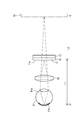
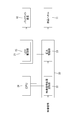
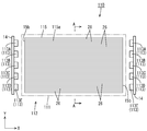
- FIG. 1 is a schematic perspective view showing a state in which a user wears a head mounted display according to Embodiment 1 of the present invention on a head.
- Schematic side view showing an optical relationship between a liquid crystal display device and a lens unit included in a head-mounted device constituting a head-mounted display, and a user's eyeball Plan view of a backlight device constituting a liquid crystal display device Cross section of liquid crystal display Cross section of LED and LED board Block diagram regarding control of liquid crystal panel and backlight device
- a goggle-type head-mounted display (HMD) HMD and a liquid crystal display device (display device) 10 used therein are exemplified.
- a part of each drawing shows an X axis, a Y axis, and a Z axis, and each axis direction is drawn to be a direction shown in each drawing.
- the goggle-type head-mounted display HMD includes a head-mounted device HMDa that is mounted so as to surround both eyes in the user's head HD.
- the head-mounted device HMDa includes a liquid crystal display device 10 that displays an image, and a lens unit that forms an image displayed on the liquid crystal display device 10 on a user's eyeball (eye) EY. At least a built-in eyepiece unit RE).
- the liquid crystal display device 10 includes at least a liquid crystal panel (display panel) 11 and a backlight device (illumination device) 12 that irradiates the liquid crystal panel 11 with light.
- the lens unit RE is disposed between the liquid crystal display device 10 and the user's eyeball EY, and imparts a refractive action to the transmitted light.
- the focal length of the lens unit RE By adjusting the focal length of the lens unit RE, the image formed on the retina (eye) EYb via the crystalline lens EYa of the eyeball EY is smaller than the actual distance L1 from the eyeball EY to the liquid crystal display device 10.
- the user can be made to recognize it as displayed on the virtual display VD that is apparently present at the position of the far distance L2.
- the user can display on the virtual display VD having a screen size (for example, about several tens of inches to several hundred inches) that is much larger than the screen size of the liquid crystal display device 10 (for example, about 0.
- the enlarged image (virtual image) is visually recognized.
- the liquid crystal display device 10 is mounted on the head-mounted device HMDa and display the right-eye image and the left-eye image on the liquid crystal display device 10
- the liquid crystal display device 10 is displayed on the head-mounted device HMDa. It is also possible to display the right-eye image on one liquid crystal display device 10 and the left-eye image on the other liquid crystal display device 10.
- illustration is abbreviate
- the liquid crystal panel 11 and the backlight device 12 constituting the liquid crystal display device 10 will be described sequentially.
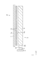
- the plate surface on the lens unit RE side is a display surface 11a for displaying an image.
- the liquid crystal panel 11 has a rectangular plate shape as a whole, and is sealed between a pair of glass substrates bonded together with a predetermined gap therebetween, and both glass substrates.
- One glass substrate array substrate, active matrix substrate
- switching elements for example, TFTs
- the pixel electrodes arranged in the region and connected to the switching element are arranged in a matrix (matrix) in a plane, and an alignment film and the like are provided.
- the other glass substrate (counter substrate, CF substrate) is provided with three color filters exhibiting R (red), G (green), and B (blue) arranged in a matrix in a predetermined arrangement.
- a light shielding layer black matrix having a substantially lattice shape, a solid counter electrode opposing the pixel electrode, an alignment film, and the like are provided so as to be arranged between adjacent color filters.
- R, G, and B color filters arranged in the X-axis direction (row direction, gate wiring extending direction) and three pixel electrodes facing each color filter have three colors. These three pixels constitute display pixels capable of color display with a predetermined gradation.
- a large number of pixels are arranged along the X-axis direction to form one pixel group, and this pixel group is arranged in a large number along the Y-axis direction (column direction).
- a large number of pixels are arranged in a matrix on the display surface 11a of the liquid crystal panel 11.
- the gate wiring described above extends along the X-axis direction, which is the arrangement direction of a large number of pixels constituting the pixel group, and collectively drives switching elements connected to the large number of pixels constituting the pixel group.
- a large number of gate wirings are individually connected to a large number of pixel groups arranged along the Y-axis direction, and along the Y-axis direction based on a signal supplied from a control board (not shown). It is possible to sequentially scan a large number of arranged pixel groups.
- the number of pixel groups arranged (number of scans) is, for example, “1080” when the liquid crystal panel 11 has 2K resolution, and “2160” when the liquid crystal panel 11 has 4K resolution.
- polarizing plates are arranged on the outer sides of both glass substrates.
- the external shape of the liquid crystal panel 11 is shown with the dashed-two dotted line.
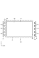
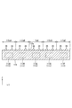
- the backlight device 12 has a horizontally long rectangular shape as a whole, and includes an LED (light source) 13, an LED substrate (light source substrate) 14 on which the LED 13 is mounted, and the LED 13. At least a light guide plate 15 that guides the light and an optical sheet (optical member) 16 that is stacked on the front side of the light guide plate 15.
- the backlight device 12 is a double-sided light input type edge light type (side light type) in which light from the LED 13 enters the light guide plate 15 from both sides.
- the long side direction coincides with the X-axis direction in each drawing
- the short side direction coincides with the Y-axis direction
- the thickness direction coincides with the Z-axis direction.
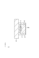
- the LED 13 is a so-called top surface emitting type in which the LED 13 is surface-mounted and the light emitting surface 13a faces away from the LED substrate 14 side.
- the LED 13 includes a blue LED element (blue light emitting element, blue LED chip) 17 that is a light source, a sealing material 18 that seals the blue LED element 17, and a blue LED element 17. And a case (housing body, housing) 19 filled with the sealing material 18.
- the blue LED element 17 is a semiconductor made of a semiconductor material such as InGaN, and emits blue light having a wavelength included in a blue wavelength region (about 420 nm to about 500 nm) when a voltage is applied in the forward direction.
- the main emission wavelength of the blue LED element 17 is preferably about 450 nm, but this is not necessarily the case.
- the sealing material 18 has a configuration in which a green phosphor and a red phosphor, both of which are not shown, are dispersed and blended at a predetermined ratio in a substantially transparent thermosetting resin material (for example, an epoxy resin material). .
- the green phosphor emits green light having a wavelength included in the green wavelength region (about 500 nm to about 570 nm) by being excited by blue light emitted from the blue LED element 17.
- the green phosphor is, for example, ⁇ -SiAlON, which is a kind of sialon phosphor, and the main emission wavelength is preferably about 540 nm, but this is not necessarily limited.
- the red phosphor emits red light having a wavelength included in a red wavelength region (about 600 nm to about 780 nm) by being excited by blue light emitted from the blue LED element 17. Details of the red phosphor will be described later in detail. Therefore, the light emitted from the LED 13 includes blue light (blue component light) emitted from the blue LED element 17, green light (green component light) emitted from the green phosphor, and red light emitted from the red phosphor. (Red component light), and generally white as a whole.
- the case 19 has a substantially box shape having an opening on the light emission side (light emission surface 13a side) as a whole, and the blue LED element 17 and the sealing material 18 are accommodated therein.
- the LED substrate 14 has a long plate shape extending along the Y-axis direction (the short side direction of the backlight device 12) and faces the light guide plate 15 side.
- a plurality of (five in FIG. 3) LEDs 13 are mounted on the plate surface at substantially equal intervals along the Y-axis direction.
- the LED boards 14 are arranged in a pair at a position sandwiching the light guide plate 15 in the X-axis direction (long side direction of the backlight device 12).
- a wiring pattern (not shown) for connecting a plurality of LEDs 13 in series is formed on the mounting surface of the LED 13 on the LED substrate 14, and the other end side of a wiring member whose one end side is connected to an external LED drive circuit board is connected A connector portion (not shown together with the wiring member) is provided.
- the light guide plate 15 is made of a synthetic resin material (for example, acrylic resin such as PMMA) having a refractive index sufficiently higher than air and substantially transparent. As shown in FIGS. 3 and 4, the light guide plate 15 has a flat plate shape, and the plate surface thereof is parallel to the plate surface (display surface 11 a) of the liquid crystal panel 11. Of the pair of plate surfaces of the light guide plate 15, the plate surface on the front side and disposed opposite to the liquid crystal panel 11 and the optical sheet 16 is a light output plate surface 15 a that emits light guided inside.
- the light guide plate 15 is disposed immediately below the liquid crystal panel 11 and the optical sheet 16, and the end surfaces on the pair of short sides of the outer peripheral end surfaces thereof are the mounting surfaces of the pair of LED substrates 14 and the respective mounting surfaces thereof.
- the light emitting surface 13a of the LED 13 is opposed to a pair of light incident end surfaces 15b on which light from the light emitting surface 13a is incident.
- the light guide plate 15 introduces light emitted from each LED 13 toward the light guide plate 15 along the X-axis direction (the alignment direction of the LEDs 13 and the light guide plate 15) from the pair of light incident end surfaces 15b, and After propagating the light inside, the light is raised to the optical sheet 16 side (front side, light emitting side) along the Z-axis direction (the alignment direction of the liquid crystal panel 11 and the optical sheet 16 and the light guide plate 15). It has a function of emitting light from the optical plate surface 15a.
- the optical sheet 16 is disposed so as to be interposed between the liquid crystal panel 11 and the light guide plate 15, thereby transmitting the light emitted from the light guide plate 15 and providing a predetermined amount of light to the transmitted light.
- the light is emitted toward the liquid crystal panel 11 while providing an optical action.
- the optical sheet 16 includes a plurality of sheets (two sheets in the present embodiment), and specific types thereof include, for example, a diffusion sheet, a lens sheet (prism sheet), a reflective polarizing sheet, and the like. It is possible to select and use as appropriate.
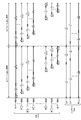
- the liquid crystal display device 10 includes a panel control unit 20 for controlling the driving of the liquid crystal panel 11 and a backlight control unit for controlling the driving of the backlight device 12 ( Lighting control unit) 21.
- the panel control unit 20 includes a video signal processing circuit unit 22 that processes a video signal, and a pixel driving unit 23 that drives each pixel based on an output signal from the video signal processing circuit unit 22. Is provided.
- the control board is provided with a CPU 24 for controlling operations of the video signal processing circuit unit 22, the pixel driving unit 23, and an LED driving unit 25 described later.
- the backlight control unit 21 includes an LED driving unit 25 that drives the LED 13 based on an output signal from the video signal processing circuit unit 22 and is provided on the LED driving circuit board.
- the operation of the LED drive unit 25 is controlled by the CPU 24 of the control board, and is synchronized with the operation of the pixel drive unit 23.
- the panel control unit 20 changes a number of pixel groups arranged along the Y-axis direction by the pixel driving unit 23 from a pixel group located at one end to a pixel group located at the other end.
- the scanning signal is sequentially supplied to a large number of gate wirings arranged along the Y-axis direction, and to the large number of source wirings arranged along the X-axis direction.
- the image signals are supplied respectively.
- the one located at one end (upper end in the vertical direction) in the Y-axis direction is referred to as a “first gate wiring”, and then the Y-axis “Second gate wiring” and “third gate wiring” are sequentially set toward the other end in the direction, and “nth gate wiring” is located at the other end (the lower end in the vertical direction) in the Y-axis direction.
- first gate wiring the one located at one end (upper end in the vertical direction) in the Y-axis direction
- nth gate wiring is located at the other end (the lower end in the vertical direction) in the Y-axis direction.
- the total scanning period for all the pixel groups is the total number of gate wirings (pixel groups). Divided number.
- the unit scanning period T1 is about 7.72 ⁇ sec (microseconds) when the liquid crystal panel 11 has 2K resolution, and in the case of 4K resolution. It is set to about 3.86 ⁇ sec.
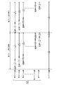
- the time required for the orientation change of the liquid crystal layer is set as a liquid crystal response time T2 ("LC" is also written in FIG. 7), and specifically, for example, about 4 msec in this embodiment.
- T2 liquid crystal response time
- each pixel included in the pixel group transmits light supplied from the backlight device 12 described below to the second alignment state of the liquid crystal molecules.
- the light is transmitted with the transmittance based on the above, and the display is performed with a predetermined gradation.
- the holding period T3 in which the second alignment state of the liquid crystal molecules is held in each pixel constituting the pixel group (also shown as “HOLD” in FIG.
- the backlight control unit 21 includes a light-off period T ⁇ b> 4 (“OFF” is also shown in FIG. 7) and a light-up period in one frame display period in the liquid crystal panel 11 whose driving is controlled by the panel control unit 20.
- the drive of each LED 13 is controlled so that T5 ("ON" is also written in FIG. 7) is included.
- the backlight control unit 21 starts the extinguishing period T4 in synchronization with the start of the one-frame display period, starts the lighting period T5 after the extinguishing period T4 ends, and ends the one-frame display period.
- the driving of each LED 13 is controlled so that the lighting period T5 ends in synchronization with the above.
- the plurality of LEDs 13 mounted on the pair of LED boards 14 are collectively controlled by the backlight control unit 21 so that the turn-off period T4 and the turn-on period T5 are the same.
- the lighting period T5 is, for example, about 1 msec.
- the turn-off period T4 is a value obtained by subtracting the turn-on period T5 from the one-frame display period, and specifically, for example, about 12.33 msec. That is, the LED 13 is turned on only for a short time before the end of the one frame display period, and is turned off at other times.
- the LED 13 is driven by a so-called impulse type by the backlight control unit 21, so that when the moving image is displayed on the liquid crystal panel 11, the afterimage is more difficult to be visually recognized by the user, and the moving image display performance is further improved. It will be excellent.
- the concrete numerical value of the light extinction period T4 and the lighting period T5 can be changed suitably.
- the red phosphor of the LED 13 includes at least a double fluoride red phosphor.
- the double fluoride red phosphor is a fluoride complex red phosphor using manganese as an activator. Specifically, for example, K 2 SiF 6 (hereinafter referred to as “KSF phosphor”) is used. .
- KSF phosphor is characterized in that the main emission wavelength is about 630 nm, for example, and both the color reproducibility and luminance related to the emitted red light are high.
- the KSF phosphor has a characteristic of continuously emitting red light for a predetermined time after the supply of blue light as excitation light from the blue LED element 17 is interrupted. There is concern about degrading the quality.
- the red phosphor of the LED 13 according to this embodiment includes a nitride red phosphor mixed with a double fluoride red phosphor.
- the nitride-based red phosphor is an alkaline earth silico-nitride red phosphor using europium as an activator. Specifically, for example, CaAlSiN 3 (hereinafter referred to as “CASN phosphor”) is used. It is done.
- the CASN phosphor has a main emission wavelength of, for example, about 650 nm, and has a color reproducibility and luminance related to the emitted red light that is lower than that of the KSF phosphor, but the afterglow time is much longer than that of the KSF phosphor. It is short, for example, about 1/100 to 1/1000.
- what mixed KSF fluorescent substance and CASN fluorescent substance with each predetermined content ratio is used for the red fluorescent substance of LED13, and the content ratio of KSF fluorescent substance is specifically 50%. While the above range is 85% or less, the CASN phosphor content ratio is 15% or more and 50% or less. According to such a configuration, the red light is difficult to be visually recognized as afterglow, while the color reproducibility and luminance related to red light are excellent. Specifically, when the content ratio of the KSF phosphor is 50% or more, or when the content ratio of the CASN phosphor is 50% or less, the content ratio of the KSF phosphor is temporarily smaller than 50%.
- the color reproducibility and the luminance relating to the red light can be maintained sufficiently high. Furthermore, when the content ratio of the KSF phosphor is 85% or less, or when the content ratio of the CASN phosphor is 15% or more, the content ratio of the KSF phosphor is temporarily larger than 85%. Compared with the case where the content ratio of the CASN phosphor is less than 15%, the afterglow of red light is less visible.
- the liquid crystal display device 10 is provided in the head-mounted device HMDa constituting the head mounted display HMD, the afterglow of red light becomes difficult to be visually recognized as described above, so that the user's operation This is suitable for displaying an image following the above without delay, and is excellent in display quality, and is less likely to cause discomfort called “VR sickness” to the user.
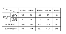
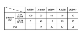
- the LED 13 was used in Example 2, and the LED 13 in which the content ratio of the KSF phosphor was 50% and the content ratio of the CASN phosphor was 50% was used as Example 3.
- the LED of Comparative Example 1 does not contain a CASN phosphor.
- the LEDs according to Comparative Examples 1 and 2 and Examples 1 to 3 are different from each other in the composition of the red phosphor, but the total amount of the red phosphor contained in the sealing material is the same, and the red phosphor It is the same also about structures (blue LED element, green fluorescent substance, etc.) other than a body.
- the LEDs according to Comparative Examples 1 and 2 and Examples 1 to 3 were applied to the liquid crystal display device 10 shown in FIGS. 3 and 4, and each LED was turned on.
- the luminance and chromaticity of the display surface 11a of the liquid crystal panel 11 were measured. The result is shown in FIG.
- the relative luminance (unit: “%”) described in FIG. 8 is a relative value when the luminance value of the display surface 11a of the liquid crystal panel 11 is 100% when the LED of Comparative Example 1 is used.
- the relative NTSC ratio (unit: “%”) described in FIG. 8 is a relative value when the NTSC ratio of the liquid crystal panel 11 is 100% when the LED of Comparative Example 1 is used.
- the NTSC ratio is a ratio based on the NTSC chromaticity region according to the NTSC (National Television System Standardization Committee) standard (100%), and the area value of the chromaticity region obtained by measurement Is a ratio obtained by dividing by the area value of the NTSC chromaticity region.
- the color reproducibility and brightness are sufficiently high.
- the content ratio of the CASN phosphor is larger than 50%, the contribution of the KSF phosphor is weakened, and it is considered that both the relative luminance and the relative NTSC ratio are decreased.
- the lower limit value of the content ratio of the KSF phosphor is preferably 50%
- the upper limit value of the content ratio of the CASN phosphor is preferably 50%.
- the content ratio of the KSF phosphor is secured to 75% or more as in Example 2
- the relative luminance is secured to 93.4% or more
- the relative NTSC ratio is secured to 94.6% or more. It can be said that reproducibility and brightness are higher. Therefore, in order to ensure higher color reproducibility and luminance, it is preferable that the content ratio of the KSF phosphor is 75% or more and the content ratio of the CASN phosphor is 25% or less.
- the evaluation is considered to be x (impossible).
- the CASN phosphor has a content ratio of 15% as in Example 1, it seems that the afterglow time of red light is further shortened and is close to the LED lighting period T5. As a result, it is difficult for the user to visually recognize the afterglow of red light, the display quality is improved, and the evaluation is considered to be ⁇ (possible).
- the CASN phosphor has a content ratio of 25% as in Example 2
- the CASN phosphor has a content ratio of 50% as in Example 3
- the residual red light remains.
- the light time is considered to be extremely short, and is considered to be shorter than the LED lighting period T5 and the liquid crystal response period T2.
- the content ratio of CASN phosphor is set to 25% and the content ratio of KSF phosphor is set to 75%. More preferably.
- the liquid crystal display device (display device) 10 includes the liquid crystal panel (display panel) 11 that can display an image, and the backlight device (illumination) that supplies light for display to the liquid crystal panel 11.
- the backlight control unit 21 that controls the driving of the LED 13 so as to include the lighting period T5 and the extinguishing period T4 in the display period, and a red phosphor are configured.
- a double fluoride red phosphor having a content ratio in the range of 50% or more and 85% or less, and a nitride system constituting the red phosphor and having a content ratio in the range of 15% or more and 50% or less
- a red phosphor A double fluoride red phosphor having a content ratio in the range of 50% or more and 85% or less, and a nitride system constituting the red phosphor and having a content ratio in the range of 15% or more and 50% or less.
- the liquid crystal panel 11 is supplied with light from the backlight device 12 from the backlight device 12 in which the drive of the LED 13 is controlled by the backlight control unit 21, and this light is used. Then, an image is displayed on the liquid crystal panel 11.
- the LED 13 of the backlight device 12 has at least a blue light emitted from the blue LED element 17 and a red phosphor that emits red light when excited by the blue light from the blue LED element 17.
- the red phosphor contains a double fluoride red phosphor, which is excellent in color reproducibility and luminance relating to red light.
- the backlight control unit 21 controls the driving of the LED 13 in synchronization with the display on the liquid crystal panel 11. More specifically, the backlight control unit 21 controls the lighting period T 5 during one frame display period on the liquid crystal panel 11. The LED 13 including the turn-off period T4 is driven. As a result, for example, when displaying a moving image on the liquid crystal panel 11, it is difficult for the user to visually recognize the afterimage, and thus the moving image display performance is excellent. On the other hand, even when the LED 13 is switched from the on state to the off state by the backlight control unit 21, among the red phosphors that the LED 13 has, the double fluoride red phosphor is supplied with blue light from the blue LED element 17.
- the red phosphor contains a nitride-based red phosphor in addition to the double fluoride red phosphor, the red light has excellent color reproducibility and luminance relating to red light. Becomes difficult to be visually recognized as afterglow. Specifically, when the content ratio of the double fluoride red phosphor is 50% or more, or when the content ratio of the nitride red phosphor is 50% or less, the double fluoride red phosphor is temporarily assumed.
- the color reproducibility and luminance relating to red light can be maintained sufficiently high. it can. Furthermore, when the content ratio of the double fluoride red phosphor is 85% or less or when the content ratio of the nitride red phosphor is 15% or more, the double fluoride red phosphor is temporarily included. Compared with the case where the ratio is larger than 85% or the case where the content ratio of the nitride-based red phosphor is smaller than 15%, the afterglow of red light is less visible.
- the double fluoride red phosphor has a content ratio of 75% or more and 85% or less, whereas the nitride-based red phosphor has a content ratio of 15% or more and 25% or less. It is made the range. In this way, when the content ratio of the double fluoride red phosphor is 75% or more, or when the content ratio of the nitride red phosphor is 25% or less, the double fluoride red fluorescence is temporarily assumed. Maintain the color reproducibility and brightness of red light sufficiently higher than when the content ratio of the body is less than 75% or when the content ratio of the nitride-based red phosphor is greater than 25%. Can do.
- the double fluoride red phosphor is temporarily included. Compared with the case where the ratio is larger than 85% and the case where the content ratio of the nitride-based red phosphor is smaller than 15%, the afterglow of red light is less visible.
- the content ratio of the double fluoride red phosphor is 85%, whereas the content ratio of the nitride red phosphor is 15%. In this way, the color reproducibility and luminance relating to the red light can be made extremely high, and the afterglow of the red light is not easily visually recognized.
- the content ratio of the double fluoride red phosphor is 75%, whereas the content ratio of the nitride-based red phosphor is 25%. In this way, the afterglow of red light is reliably prevented from being visually recognized.
- the double fluoride red phosphor is a fluoride complex red phosphor using manganese as an activator. This is suitable for keeping the color reproducibility and luminance related to red light high.
- the nitride-based red phosphor is an alkaline earth silico-nitride red phosphor using europium as an activator. This is suitable for making it difficult to visually recognize the afterglow associated with red light.
- the backlight control unit 21 starts the turn-off period T4 in synchronization with the start of the one-frame display period, starts the turn-on period T5 after the turn-off period T4 ends, and synchronizes with the end of the one-frame display period. Then, the driving of the LED 13 is controlled so that the lighting period T5 ends.
- the LED 13 is driven by the backlight controller 21 by the impulse type, for example, when displaying a moving image on the liquid crystal panel 11, the afterimage is more difficult to be visually recognized by the user, and thus the moving image display performance is more excellent. It becomes.
- the head mounted display HMD includes the liquid crystal display device 10 described above, a lens unit RE that forms an image displayed on the liquid crystal display device 10 on a user's eyeball (eye) EY, and a liquid crystal display.
- the head mounting device HMDa that includes the display device 10 and the lens unit RE and is mounted on the user's head HD is provided.
- the head mounted display HMD having such a configuration, when the user uses the head-mounted device HMDa mounted on the head HD, the image displayed on the liquid crystal display device 10 is displayed on the user by the lens unit RE. The image is formed on the eyeball EY, so that the user can visually recognize the image displayed on the liquid crystal display device 10 in an enlarged form.
- liquid crystal display device 10 provided in the head-mounted device HMDa is difficult to visually recognize the afterglow of red light, it is suitable for displaying an image following the operation of the user without delay, and is excellent in display quality. At the same time, the user is less likely to experience discomfort called “VR sickness”.
- Embodiment 2 A second embodiment of the present invention will be described with reference to FIGS. In this Embodiment 2, what changed the structure and control of the backlight apparatus 112 is shown. In addition, the overlapping description about the same structure, operation
- the light guide plate 115 constituting the backlight device 112 is provided with a prism (directional light guide) 26 on the light output plate surface 115a.
- the prism 26 has a mountain shape with a substantially triangular (substantially right-angled triangle) cross-sectional shape, and is a protrusion that extends linearly along the X-axis direction (the normal direction of the light emitting surface 113a of the LED 113).
- a plurality of light emitting plate surfaces 115a are arranged side by side along the Y-axis direction in the plane of the light output plate surface 115a.
- the prism 26 Since the prism 26 has an apex angle set substantially at right angles, the light propagating through the light guide plate 115 and totally reflected at the interface of the prism 26 has a Y-axis direction (alignment of the LEDs 113) in the light guide plate 115.
- directivity is provided so as to travel substantially straight along the X-axis direction. That is, the prism 26 imparts directivity that restricts light introduced from the LED 113 into the light guide plate 115 from diffusing in the Y-axis direction.
- the light exit plate surface 115a of the light guide plate 115 is divided into five horizontally long belt-like regions that are the same as the number of LEDs 113 arranged, and these five divided regions are selectively selected according to the lighting of the five LEDs 113. Flashes.
- the five LEDs 113 arranged in the Y-axis direction are referred to as a first LED 113A, a second LED 113B, a third LED 113C, a fourth LED 113D, and a fifth LED 113E in order from the top shown in FIG. 10 (left side shown in FIG. 11). Accordingly, the light of the first divided region 115aA and the second LED 113B that emits the light of the first LED 113A in the five divided regions on the light output plate surface 115a of the light guide plate 115 from the top shown in FIG. 10 (left side shown in FIG. 11).
- the second partitioned region 115aB that emits the light the third partitioned region 115aC that emits the light of the third LED 113C, the fourth partitioned region 115aD that emits the light of the fourth LED 113D, and the fifth partitioned region 115aE that emits the light of the fifth LED 113E.
- the light emitted from each of the divided regions 115aA to 115aE on the light exit plate surface 115a of the light guide plate 115 is a specific plurality of pixel groups among a large number of pixel groups included in the liquid crystal panel 111. Will be selectively supplied. That is, the large number of pixel groups provided in the liquid crystal panel 111 includes a first pixel group including a plurality of pixel groups that are overlapped with the first segmented region 115aA and selectively supplied with light from the first segmented region 115aA.
- a second pixel group consisting of a plurality of pixel groups that are selectively supplied with light from the second segmented region 115aB and superimposed on the second segmented region 115aB, and a third segmented region 115aC superimposed on the third segmented region 115aC.
- a third pixel group consisting of a plurality of pixel groups to which light of a predetermined amount is supplied and from a plurality of pixel groups to which light from the fourth partitioned region 115aD is selectively supplied in an overlapping manner with the fourth partitioned region 115aD
- a fifth pixel group composed of a plurality of pixel groups that are selectively supplied with light from the fifth segmented region 115aE so as to overlap the fifth segmented region 115aE.
- the total number of gate wirings is n, and the one located at one end in the Y-axis direction is referred to as the “first gate wiring” and is located at the other end in the Y-axis direction.
- the first pixel group is scanned by the (n / 5) th gate wiring from the first gate wiring, and the second pixel group is scanned by the (n / 5 + 1) th gate wiring.
- the third pixel group is scanned from the (2n / 5 + 1) gate wiring to the (3n / 5) gate wiring, and the fourth pixel group is scanned to the (3n / 5th) gate wiring.
- the 5 + 1) gate wiring is scanned by the (4n / 5) gate wiring
- the fifth pixel group is scanned by the (4n / 5 + 1) gate wiring by the nth gate wiring.
- a plurality of pixel groups are sequentially scanned by a panel control unit (both backlight control units are not shown in this embodiment, but refer to FIG. 6).
- the driving of the plurality of LEDs 113 is controlled in synchronism with the driving of the pixel group to be supplied with light so that the extinguishing period T4 and the lighting period T5 are included while being driven.
- the second alignment state of the liquid crystal molecules is maintained as the plurality of pixel groups constituting the first pixel group are scanned and driven by the (n / 5) th gate line from the first gate line.
- the first LED 113A of the backlight device 112 is in the extinguishing period T4 until reaching the holding period T3, and after a predetermined time has elapsed since reaching the holding period T3, the first LED 113A shifts to the lighting period T5.
- the second LED 113B of the backlight device 112 is set to the extinguishing period T4, and after a predetermined time has elapsed since reaching the holding period T3, the second LED 113B shifts to the lighting period T5.
- the lighting period T5 of the second LED 113B is started later than the lighting period T5 of the first LED 113A.
- the timing of the turn-off period T4 and the turn-on period T5 of the third LED 113C, the fourth LED 113D, and the fifth LED 113E is also determined in synchronization with the scanning and driving of the third pixel group, the fourth pixel group, and the fifth pixel group in the same manner as described above. .
- the lighting periods T5 of the LEDs 113A to 113E are all equal, and a part thereof extends over the first frame display period and the second frame display period.
- the backlight control unit controls the driving of the LEDs 113A to 113E in synchronization with the scanning of the pixel groups by the panel control unit, so that an afterimage is displayed to the user when displaying a moving image on the liquid crystal panel 111. It becomes harder to see, and the moving image display performance becomes better.
- the red phosphor of the LED 113 is a mixture of a KSF phosphor and a CASN phosphor, and the content ratio of the KSF phosphor is 50% or more and 85% or less.
- the content ratio of the CASN phosphor is 15% or more and 50% or less, sufficient color reproducibility and luminance of red light can be obtained, and afterglow of red light is suppressed.
- the panel control unit (see FIG. 6) that controls the driving of the liquid crystal panel 111 is provided, and the liquid crystal panel 111 includes a plurality of pixels arranged in a matrix.
- the panel control unit sequentially scans a pixel group including a plurality of pixels arranged in the row direction along the column direction during one frame display period, and the backlight device 112 includes a plurality of pixels.
- the plurality of LEDs 113 are arranged so as to selectively supply light to a plurality of pixel groups, and the backlight control unit (see FIG. 6) controls the plurality of pixel groups.
- the plurality of LEDs 113 are driven in synchronism with the driving of the pixel group to be supplied with light so that the lighting period T5 and the extinguishing period T4 are included while being sequentially driven by the scanning unit. Control .
- the backlight controller controls the driving of the LED 113 in synchronization with the scanning of the plurality of pixel groups by the panel controller, for example, when displaying a moving image on the liquid crystal panel 111, the afterimage is more visually recognized by the user. As a result, the moving image display performance is improved.
- the KSNAF phosphor K 2 Si 1-x Na x Al x F 6 : Mn
- KTF phosphor K 2 TiF 6 : Mn
- the red phosphor is composed of only two types of KSF phosphor and CASN phosphor.
- another red phosphor is included in the KSF phosphor and CASN phosphor. It is also possible to use three or more types.
- the red phosphor to be added is preferably a double fluoride red phosphor or a nitride red phosphor, but this is not necessarily the case.
- the material of the blue LED element and the green phosphor constituting the LED, the green phosphor, the main emission wavelength, and the like can be appropriately changed.
- a yellow phosphor can be included in the sealing material.
- the pair of LED substrates (LEDs) is disposed in a form facing the pair of short-side end surfaces of the light guide plate.
- a pair of LED substrates (LEDs) may be arranged so as to face the pair of long side end faces of the light guide plate.
- the LED substrate (LED) may be arranged in a form facing only one end surface on the short side or the long side of the outer peripheral end surface of the light guide plate.
- the arrangement and the number of LED substrates (LEDs) with respect to the outer peripheral end surface of the light guide plate can be appropriately changed.
- the backlight control unit is provided on the LED drive circuit board.
- the LED drive circuit board may be omitted and the backlight control unit may be provided on the control board. I do not care.
- the liquid crystal display device including the liquid crystal panel is illustrated, but other types of display panels (PDP (plasma display panel), organic EL panel, EPD (electrophoretic display panel), MEMS ( The present invention can also be applied to a display device equipped with a display panel (Micro Electro Mechanical Systems).
- PDP plasma display panel
- EPD electrostatic display panel
- MEMS MEMS
- the present invention can also be applied to a display device equipped with a display panel (Micro Electro Mechanical Systems).
- a head-mounted display is shown. However, the present invention is applied to a head-up display, a projector, and the like as a device that enlarges and displays an image displayed on a liquid crystal panel using a lens or the like. Applicable.
- the present invention is also applicable to liquid crystal display devices that do not have an enlarged display function (such as a television receiver, a tablet terminal, and a smartphone).
- the planar shape of the liquid crystal display device (liquid crystal panel or backlight device) is a horizontally long rectangle is shown.
- the planar shape of the liquid crystal display device is a square, an octagon, or the like. It may be a pentagon or more polygon, a vertically long rectangle, a circle, a semicircle, an oval, an ellipse, a trapezoid, or the like.
- the top-emitting LED is shown, but a side-emitting LED can be used as the light source.
- the case where the light-emitting plate surface of the light guide plate is made flat has been shown.
- a lenticular lens portion made of a protrusion having a semicircular cross section (saddle shape).
- the reflective dots scatter and reflect light propagating in the light guide plate to promote light output from the light output plate surface, and the distribution pattern makes the luminance distribution related to the light emitted from the light output plate surface uniform. It has been adjusted.
- the structure which concerns on a light-guide plate can be changed suitably.
Landscapes
- Chemical & Material Sciences (AREA)
- Physics & Mathematics (AREA)
- Engineering & Computer Science (AREA)
- General Physics & Mathematics (AREA)
- Inorganic Chemistry (AREA)
- Materials Engineering (AREA)
- Organic Chemistry (AREA)
- Optics & Photonics (AREA)
- Computer Hardware Design (AREA)
- Nonlinear Science (AREA)
- Theoretical Computer Science (AREA)
- Microelectronics & Electronic Packaging (AREA)
- Crystallography & Structural Chemistry (AREA)
- Mathematical Physics (AREA)
- Manufacturing & Machinery (AREA)
- Power Engineering (AREA)
- Liquid Crystal Display Device Control (AREA)
- Liquid Crystal (AREA)
- Control Of Indicators Other Than Cathode Ray Tubes (AREA)
Abstract
Selon la présente invention, un appareil d'affichage à cristaux liquides (10) comprend : un panneau à cristaux liquides (11) ; un dispositif de rétroéclairage (12) ; une DEL (13) ayant au moins un élément de DEL bleue (17) permettant d'émettre une lumière bleue et un phosphore rouge permettant d'émettre une lumière rouge par excitation associée au moyen d'une lumière bleue provenant de l'élément de DEL bleue (17) ; une unité de commande de rétroéclairage (21) permettant de commander l'entraînement de la DEL (13) en synchronisme avec l'affichage par le panneau à cristaux liquides (11), l'unité de commande de rétroéclairage (21) commandant l'entraînement de la DEL (13) de telle sorte qu'une période d'allumage et une période d'extinction sont comprises dans une période d'affichage à une seule trame dans le panneau à cristaux liquides (11) ; un phosphore rouge de fluorure complexe constituant une partie du phosphore rouge et étant dans une plage de rapport de teneur variant de 50 à 85 % ; et un phosphore rouge à base de nitrure constituant une partie du phosphore rouge et étant dans une plage de teneur variant de 15 à 50 %.
Priority Applications (4)
| Application Number | Priority Date | Filing Date | Title |
|---|---|---|---|
| US16/497,813 US10775627B2 (en) | 2017-03-30 | 2018-03-30 | Display device and head-mounted display |
| EP18774996.5A EP3605215A4 (fr) | 2017-03-30 | 2018-03-30 | Appareil d'affichage et visiocasque |
| CN201880021510.3A CN110476112B (zh) | 2017-03-30 | 2018-03-30 | 显示装置和头戴显示器 |
| US16/988,753 US11048092B2 (en) | 2017-03-30 | 2020-08-10 | Display device and head-mounted display |
Applications Claiming Priority (2)
| Application Number | Priority Date | Filing Date | Title |
|---|---|---|---|
| JP2017-067299 | 2017-03-30 | ||
| JP2017067299 | 2017-03-30 |
Related Child Applications (2)
| Application Number | Title | Priority Date | Filing Date |
|---|---|---|---|
| US16/497,813 A-371-Of-International US10775627B2 (en) | 2017-03-30 | 2018-03-30 | Display device and head-mounted display |
| US16/988,753 Continuation US11048092B2 (en) | 2017-03-30 | 2020-08-10 | Display device and head-mounted display |
Publications (1)
| Publication Number | Publication Date |
|---|---|
| WO2018181908A1 true WO2018181908A1 (fr) | 2018-10-04 |
Family
ID=63676505
Family Applications (1)
| Application Number | Title | Priority Date | Filing Date |
|---|---|---|---|
| PCT/JP2018/013647 WO2018181908A1 (fr) | 2017-03-30 | 2018-03-30 | Appareil d'affichage et visiocasque |
Country Status (4)
| Country | Link |
|---|---|
| US (2) | US10775627B2 (fr) |
| EP (1) | EP3605215A4 (fr) |
| CN (1) | CN110476112B (fr) |
| WO (1) | WO2018181908A1 (fr) |
Cited By (1)
| Publication number | Priority date | Publication date | Assignee | Title |
|---|---|---|---|---|
| US11263981B2 (en) | 2019-05-31 | 2022-03-01 | Sharp Kabushiki Kaisha | Display device and head-mounted display |
Families Citing this family (2)
| Publication number | Priority date | Publication date | Assignee | Title |
|---|---|---|---|---|
| US11635622B1 (en) * | 2018-12-07 | 2023-04-25 | Meta Platforms Technologies, Llc | Nanovided spacer materials and corresponding systems and methods |
| US10895777B1 (en) * | 2019-09-24 | 2021-01-19 | Coretronic Corporation | Display device and method for adjusting chromaticity of display beam |
Citations (5)
| Publication number | Priority date | Publication date | Assignee | Title |
|---|---|---|---|---|
| JP2004157373A (ja) * | 2002-11-07 | 2004-06-03 | Sharp Corp | 液晶表示装置 |
| JP2004206044A (ja) | 2002-10-29 | 2004-07-22 | Fujitsu Display Technologies Corp | 照明装置及びそれを用いた液晶表示装置 |
| JP2011227490A (ja) * | 2010-03-31 | 2011-11-10 | Sharp Corp | 液晶表示装置及びテレビジョン受信装置 |
| JP2012104814A (ja) * | 2010-10-15 | 2012-05-31 | Mitsubishi Chemicals Corp | 白色発光装置及び照明器具 |
| JP2015194636A (ja) * | 2014-03-31 | 2015-11-05 | シャープ株式会社 | 照明装置、表示装置及びテレビ受信装置 |
Family Cites Families (6)
| Publication number | Priority date | Publication date | Assignee | Title |
|---|---|---|---|---|
| JP2002207463A (ja) * | 2000-11-13 | 2002-07-26 | Mitsubishi Electric Corp | 液晶表示装置 |
| KR100728007B1 (ko) | 2005-10-26 | 2007-06-14 | 삼성전자주식회사 | 액정 표시 장치 및 액정 표시 장치의 구동 방법 |
| JPWO2009110285A1 (ja) * | 2008-03-03 | 2011-07-14 | シャープ株式会社 | 発光装置 |
| JP6151373B2 (ja) * | 2013-11-08 | 2017-06-21 | シャープ株式会社 | 発光装置、及び照明装置 |
| US10381528B2 (en) * | 2015-08-31 | 2019-08-13 | Sharp Kabushiki Kaisha | Image display apparatus |
| KR20160018636A (ko) * | 2016-01-29 | 2016-02-17 | 우리이앤엘 주식회사 | 표시 장치 |
-
2018
- 2018-03-30 EP EP18774996.5A patent/EP3605215A4/fr active Pending
- 2018-03-30 CN CN201880021510.3A patent/CN110476112B/zh active Active
- 2018-03-30 US US16/497,813 patent/US10775627B2/en active Active
- 2018-03-30 WO PCT/JP2018/013647 patent/WO2018181908A1/fr unknown
-
2020
- 2020-08-10 US US16/988,753 patent/US11048092B2/en active Active
Patent Citations (5)
| Publication number | Priority date | Publication date | Assignee | Title |
|---|---|---|---|---|
| JP2004206044A (ja) | 2002-10-29 | 2004-07-22 | Fujitsu Display Technologies Corp | 照明装置及びそれを用いた液晶表示装置 |
| JP2004157373A (ja) * | 2002-11-07 | 2004-06-03 | Sharp Corp | 液晶表示装置 |
| JP2011227490A (ja) * | 2010-03-31 | 2011-11-10 | Sharp Corp | 液晶表示装置及びテレビジョン受信装置 |
| JP2012104814A (ja) * | 2010-10-15 | 2012-05-31 | Mitsubishi Chemicals Corp | 白色発光装置及び照明器具 |
| JP2015194636A (ja) * | 2014-03-31 | 2015-11-05 | シャープ株式会社 | 照明装置、表示装置及びテレビ受信装置 |
Non-Patent Citations (1)
| Title |
|---|
| See also references of EP3605215A4 |
Cited By (1)
| Publication number | Priority date | Publication date | Assignee | Title |
|---|---|---|---|---|
| US11263981B2 (en) | 2019-05-31 | 2022-03-01 | Sharp Kabushiki Kaisha | Display device and head-mounted display |
Also Published As
| Publication number | Publication date |
|---|---|
| EP3605215A4 (fr) | 2020-08-12 |
| US20210096374A1 (en) | 2021-04-01 |
| US11048092B2 (en) | 2021-06-29 |
| CN110476112A (zh) | 2019-11-19 |
| CN110476112B (zh) | 2022-07-19 |
| US20200089000A1 (en) | 2020-03-19 |
| US10775627B2 (en) | 2020-09-15 |
| EP3605215A1 (fr) | 2020-02-05 |
Similar Documents
| Publication | Publication Date | Title |
|---|---|---|
| WO2020248631A1 (fr) | Appareil d'affichage à cristaux liquides | |
| JP5436050B2 (ja) | 立体映像表示装置 | |
| US11048092B2 (en) | Display device and head-mounted display | |
| KR100964467B1 (ko) | 디스플레이 장치 | |
| US7742123B2 (en) | Color-filterless LCD | |
| KR101460171B1 (ko) | 광학 부재, 이를 포함하는 백라이트 어셈블리 및 표시 장치 | |
| EP2579240B1 (fr) | Dispositif d'affichage à cristaux liquides et récepteur de télévision | |
| JP2010020961A (ja) | 面状光源及び液晶表示装置 | |
| WO2011048830A1 (fr) | Dispositif de rétro-éclairage, appareil d'affichage d'images comprenant celui-ci, et procédé de contrôle | |
| US20100149225A1 (en) | Illuminator and display having same | |
| US20170004782A1 (en) | Liquid crystal display device | |
| US9552782B2 (en) | Image display device, presentation box employing same, and method of driving image display device | |
| US20120075555A1 (en) | Liquid crystal display apparatus and light emitting assembly with light transmission control elements for illuminating same | |
| WO2014087875A1 (fr) | Dispositif d'affichage et dispositif de réception de télévision | |
| JP2006236701A (ja) | バックライト装置及び液晶表示装置 | |
| US20150262520A1 (en) | Image display device and drive method therefor | |
| EP1705927A1 (fr) | Dispositif d'affichage autostéréoscopique utilisant la méthode à séquence temporelle | |
| JP3810788B2 (ja) | 表示装置 | |
| KR102342716B1 (ko) | 표시장치 및 이의 구동방법 | |
| WO2012073795A1 (fr) | Dispositif d'affichage, son procédé de pilotage et appareil électronique | |
| KR20060065377A (ko) | 액정 표시 장치 | |
| KR20160145878A (ko) | 액정 표시 장치 | |
| JP4421575B2 (ja) | 表示装置 | |
| JP2006058483A (ja) | 液晶表示用バックライト装置及び透過型液晶表示装置 | |
| JP5397334B2 (ja) | 表示装置の駆動方法 |
Legal Events
| Date | Code | Title | Description |
|---|---|---|---|
| 121 | Ep: the epo has been informed by wipo that ep was designated in this application |
Ref document number: 18774996 Country of ref document: EP Kind code of ref document: A1 |
|
| NENP | Non-entry into the national phase |
Ref country code: DE |
|
| ENP | Entry into the national phase |
Ref document number: 2018774996 Country of ref document: EP Effective date: 20191030 |
|
| NENP | Non-entry into the national phase |
Ref country code: JP |