WO2018181908A1 - Display apparatus and head-mounted display - Google Patents
Display apparatus and head-mounted display Download PDFInfo
- Publication number
- WO2018181908A1 WO2018181908A1 PCT/JP2018/013647 JP2018013647W WO2018181908A1 WO 2018181908 A1 WO2018181908 A1 WO 2018181908A1 JP 2018013647 W JP2018013647 W JP 2018013647W WO 2018181908 A1 WO2018181908 A1 WO 2018181908A1
- Authority
- WO
- WIPO (PCT)
- Prior art keywords
- light
- red phosphor
- display
- period
- content ratio
- Prior art date
Links
Images

Classifications
-
- G—PHYSICS
- G02—OPTICS
- G02B—OPTICAL ELEMENTS, SYSTEMS OR APPARATUS
- G02B27/00—Optical systems or apparatus not provided for by any of the groups G02B1/00 - G02B26/00, G02B30/00
- G02B27/01—Head-up displays
- G02B27/017—Head mounted
- G02B27/0172—Head mounted characterised by optical features
-
- C—CHEMISTRY; METALLURGY
- C09—DYES; PAINTS; POLISHES; NATURAL RESINS; ADHESIVES; COMPOSITIONS NOT OTHERWISE PROVIDED FOR; APPLICATIONS OF MATERIALS NOT OTHERWISE PROVIDED FOR
- C09K—MATERIALS FOR MISCELLANEOUS APPLICATIONS, NOT PROVIDED FOR ELSEWHERE
- C09K11/00—Luminescent, e.g. electroluminescent, chemiluminescent materials
- C09K11/08—Luminescent, e.g. electroluminescent, chemiluminescent materials containing inorganic luminescent materials
- C09K11/67—Luminescent, e.g. electroluminescent, chemiluminescent materials containing inorganic luminescent materials containing refractory metals
- C09K11/674—Halogenides
- C09K11/675—Halogenides with alkali or alkaline earth metals
-
- C—CHEMISTRY; METALLURGY
- C09—DYES; PAINTS; POLISHES; NATURAL RESINS; ADHESIVES; COMPOSITIONS NOT OTHERWISE PROVIDED FOR; APPLICATIONS OF MATERIALS NOT OTHERWISE PROVIDED FOR
- C09K—MATERIALS FOR MISCELLANEOUS APPLICATIONS, NOT PROVIDED FOR ELSEWHERE
- C09K11/00—Luminescent, e.g. electroluminescent, chemiluminescent materials
- C09K11/08—Luminescent, e.g. electroluminescent, chemiluminescent materials containing inorganic luminescent materials
- C09K11/64—Luminescent, e.g. electroluminescent, chemiluminescent materials containing inorganic luminescent materials containing aluminium
- C09K11/644—Halogenides
- C09K11/645—Halogenides with alkali or alkaline earth metals
-
- C—CHEMISTRY; METALLURGY
- C09—DYES; PAINTS; POLISHES; NATURAL RESINS; ADHESIVES; COMPOSITIONS NOT OTHERWISE PROVIDED FOR; APPLICATIONS OF MATERIALS NOT OTHERWISE PROVIDED FOR
- C09K—MATERIALS FOR MISCELLANEOUS APPLICATIONS, NOT PROVIDED FOR ELSEWHERE
- C09K11/00—Luminescent, e.g. electroluminescent, chemiluminescent materials
- C09K11/08—Luminescent, e.g. electroluminescent, chemiluminescent materials containing inorganic luminescent materials
- C09K11/77—Luminescent, e.g. electroluminescent, chemiluminescent materials containing inorganic luminescent materials containing rare earth metals
- C09K11/7728—Luminescent, e.g. electroluminescent, chemiluminescent materials containing inorganic luminescent materials containing rare earth metals containing europium
- C09K11/77348—Silicon Aluminium Nitrides or Silicon Aluminium Oxynitrides
-
- G—PHYSICS
- G02—OPTICS
- G02F—OPTICAL DEVICES OR ARRANGEMENTS FOR THE CONTROL OF LIGHT BY MODIFICATION OF THE OPTICAL PROPERTIES OF THE MEDIA OF THE ELEMENTS INVOLVED THEREIN; NON-LINEAR OPTICS; FREQUENCY-CHANGING OF LIGHT; OPTICAL LOGIC ELEMENTS; OPTICAL ANALOGUE/DIGITAL CONVERTERS
- G02F1/00—Devices or arrangements for the control of the intensity, colour, phase, polarisation or direction of light arriving from an independent light source, e.g. switching, gating or modulating; Non-linear optics
- G02F1/01—Devices or arrangements for the control of the intensity, colour, phase, polarisation or direction of light arriving from an independent light source, e.g. switching, gating or modulating; Non-linear optics for the control of the intensity, phase, polarisation or colour
- G02F1/13—Devices or arrangements for the control of the intensity, colour, phase, polarisation or direction of light arriving from an independent light source, e.g. switching, gating or modulating; Non-linear optics for the control of the intensity, phase, polarisation or colour based on liquid crystals, e.g. single liquid crystal display cells
- G02F1/133—Constructional arrangements; Operation of liquid crystal cells; Circuit arrangements
- G02F1/1333—Constructional arrangements; Manufacturing methods
- G02F1/1335—Structural association of cells with optical devices, e.g. polarisers or reflectors
- G02F1/1336—Illuminating devices
-
- G—PHYSICS
- G09—EDUCATION; CRYPTOGRAPHY; DISPLAY; ADVERTISING; SEALS
- G09G—ARRANGEMENTS OR CIRCUITS FOR CONTROL OF INDICATING DEVICES USING STATIC MEANS TO PRESENT VARIABLE INFORMATION
- G09G3/00—Control arrangements or circuits, of interest only in connection with visual indicators other than cathode-ray tubes
- G09G3/001—Control arrangements or circuits, of interest only in connection with visual indicators other than cathode-ray tubes using specific devices not provided for in groups G09G3/02 - G09G3/36, e.g. using an intermediate record carrier such as a film slide; Projection systems; Display of non-alphanumerical information, solely or in combination with alphanumerical information, e.g. digital display on projected diapositive as background
- G09G3/002—Control arrangements or circuits, of interest only in connection with visual indicators other than cathode-ray tubes using specific devices not provided for in groups G09G3/02 - G09G3/36, e.g. using an intermediate record carrier such as a film slide; Projection systems; Display of non-alphanumerical information, solely or in combination with alphanumerical information, e.g. digital display on projected diapositive as background to project the image of a two-dimensional display, such as an array of light emitting or modulating elements or a CRT
-
- G—PHYSICS
- G09—EDUCATION; CRYPTOGRAPHY; DISPLAY; ADVERTISING; SEALS
- G09G—ARRANGEMENTS OR CIRCUITS FOR CONTROL OF INDICATING DEVICES USING STATIC MEANS TO PRESENT VARIABLE INFORMATION
- G09G3/00—Control arrangements or circuits, of interest only in connection with visual indicators other than cathode-ray tubes
- G09G3/20—Control arrangements or circuits, of interest only in connection with visual indicators other than cathode-ray tubes for presentation of an assembly of a number of characters, e.g. a page, by composing the assembly by combination of individual elements arranged in a matrix no fixed position being assigned to or needed to be assigned to the individual characters or partial characters
- G09G3/34—Control arrangements or circuits, of interest only in connection with visual indicators other than cathode-ray tubes for presentation of an assembly of a number of characters, e.g. a page, by composing the assembly by combination of individual elements arranged in a matrix no fixed position being assigned to or needed to be assigned to the individual characters or partial characters by control of light from an independent source
- G09G3/3406—Control of illumination source
-
- H—ELECTRICITY
- H01—ELECTRIC ELEMENTS
- H01L—SEMICONDUCTOR DEVICES NOT COVERED BY CLASS H10
- H01L33/00—Semiconductor devices with at least one potential-jump barrier or surface barrier specially adapted for light emission; Processes or apparatus specially adapted for the manufacture or treatment thereof or of parts thereof; Details thereof
- H01L33/48—Semiconductor devices with at least one potential-jump barrier or surface barrier specially adapted for light emission; Processes or apparatus specially adapted for the manufacture or treatment thereof or of parts thereof; Details thereof characterised by the semiconductor body packages
- H01L33/50—Wavelength conversion elements
- H01L33/501—Wavelength conversion elements characterised by the materials, e.g. binder
- H01L33/502—Wavelength conversion materials
-
- G—PHYSICS
- G02—OPTICS
- G02B—OPTICAL ELEMENTS, SYSTEMS OR APPARATUS
- G02B27/00—Optical systems or apparatus not provided for by any of the groups G02B1/00 - G02B26/00, G02B30/00
- G02B27/01—Head-up displays
- G02B27/0101—Head-up displays characterised by optical features
- G02B2027/0112—Head-up displays characterised by optical features comprising device for genereting colour display
-
- G—PHYSICS
- G02—OPTICS
- G02B—OPTICAL ELEMENTS, SYSTEMS OR APPARATUS
- G02B6/00—Light guides; Structural details of arrangements comprising light guides and other optical elements, e.g. couplings
- G02B6/0001—Light guides; Structural details of arrangements comprising light guides and other optical elements, e.g. couplings specially adapted for lighting devices or systems
- G02B6/0011—Light guides; Structural details of arrangements comprising light guides and other optical elements, e.g. couplings specially adapted for lighting devices or systems the light guides being planar or of plate-like form
- G02B6/0013—Means for improving the coupling-in of light from the light source into the light guide
-
- G—PHYSICS
- G02—OPTICS
- G02B—OPTICAL ELEMENTS, SYSTEMS OR APPARATUS
- G02B6/00—Light guides; Structural details of arrangements comprising light guides and other optical elements, e.g. couplings
- G02B6/0001—Light guides; Structural details of arrangements comprising light guides and other optical elements, e.g. couplings specially adapted for lighting devices or systems
- G02B6/0011—Light guides; Structural details of arrangements comprising light guides and other optical elements, e.g. couplings specially adapted for lighting devices or systems the light guides being planar or of plate-like form
- G02B6/0033—Means for improving the coupling-out of light from the light guide
- G02B6/0035—Means for improving the coupling-out of light from the light guide provided on the surface of the light guide or in the bulk of it
- G02B6/0038—Linear indentations or grooves, e.g. arc-shaped grooves or meandering grooves, extending over the full length or width of the light guide
-
- G—PHYSICS
- G02—OPTICS
- G02B—OPTICAL ELEMENTS, SYSTEMS OR APPARATUS
- G02B6/00—Light guides; Structural details of arrangements comprising light guides and other optical elements, e.g. couplings
- G02B6/0001—Light guides; Structural details of arrangements comprising light guides and other optical elements, e.g. couplings specially adapted for lighting devices or systems
- G02B6/0011—Light guides; Structural details of arrangements comprising light guides and other optical elements, e.g. couplings specially adapted for lighting devices or systems the light guides being planar or of plate-like form
- G02B6/0066—Light guides; Structural details of arrangements comprising light guides and other optical elements, e.g. couplings specially adapted for lighting devices or systems the light guides being planar or of plate-like form characterised by the light source being coupled to the light guide
- G02B6/0068—Arrangements of plural sources, e.g. multi-colour light sources
-
- G—PHYSICS
- G02—OPTICS
- G02F—OPTICAL DEVICES OR ARRANGEMENTS FOR THE CONTROL OF LIGHT BY MODIFICATION OF THE OPTICAL PROPERTIES OF THE MEDIA OF THE ELEMENTS INVOLVED THEREIN; NON-LINEAR OPTICS; FREQUENCY-CHANGING OF LIGHT; OPTICAL LOGIC ELEMENTS; OPTICAL ANALOGUE/DIGITAL CONVERTERS
- G02F1/00—Devices or arrangements for the control of the intensity, colour, phase, polarisation or direction of light arriving from an independent light source, e.g. switching, gating or modulating; Non-linear optics
- G02F1/01—Devices or arrangements for the control of the intensity, colour, phase, polarisation or direction of light arriving from an independent light source, e.g. switching, gating or modulating; Non-linear optics for the control of the intensity, phase, polarisation or colour
- G02F1/13—Devices or arrangements for the control of the intensity, colour, phase, polarisation or direction of light arriving from an independent light source, e.g. switching, gating or modulating; Non-linear optics for the control of the intensity, phase, polarisation or colour based on liquid crystals, e.g. single liquid crystal display cells
- G02F1/133—Constructional arrangements; Operation of liquid crystal cells; Circuit arrangements
- G02F1/1333—Constructional arrangements; Manufacturing methods
- G02F1/1335—Structural association of cells with optical devices, e.g. polarisers or reflectors
- G02F1/1336—Illuminating devices
- G02F1/133601—Illuminating devices for spatial active dimming
-
- G—PHYSICS
- G02—OPTICS
- G02F—OPTICAL DEVICES OR ARRANGEMENTS FOR THE CONTROL OF LIGHT BY MODIFICATION OF THE OPTICAL PROPERTIES OF THE MEDIA OF THE ELEMENTS INVOLVED THEREIN; NON-LINEAR OPTICS; FREQUENCY-CHANGING OF LIGHT; OPTICAL LOGIC ELEMENTS; OPTICAL ANALOGUE/DIGITAL CONVERTERS
- G02F1/00—Devices or arrangements for the control of the intensity, colour, phase, polarisation or direction of light arriving from an independent light source, e.g. switching, gating or modulating; Non-linear optics
- G02F1/01—Devices or arrangements for the control of the intensity, colour, phase, polarisation or direction of light arriving from an independent light source, e.g. switching, gating or modulating; Non-linear optics for the control of the intensity, phase, polarisation or colour
- G02F1/13—Devices or arrangements for the control of the intensity, colour, phase, polarisation or direction of light arriving from an independent light source, e.g. switching, gating or modulating; Non-linear optics for the control of the intensity, phase, polarisation or colour based on liquid crystals, e.g. single liquid crystal display cells
- G02F1/133—Constructional arrangements; Operation of liquid crystal cells; Circuit arrangements
- G02F1/1333—Constructional arrangements; Manufacturing methods
- G02F1/1335—Structural association of cells with optical devices, e.g. polarisers or reflectors
- G02F1/1336—Illuminating devices
- G02F1/133614—Illuminating devices using photoluminescence, e.g. phosphors illuminated by UV or blue light
-
- G—PHYSICS
- G02—OPTICS
- G02F—OPTICAL DEVICES OR ARRANGEMENTS FOR THE CONTROL OF LIGHT BY MODIFICATION OF THE OPTICAL PROPERTIES OF THE MEDIA OF THE ELEMENTS INVOLVED THEREIN; NON-LINEAR OPTICS; FREQUENCY-CHANGING OF LIGHT; OPTICAL LOGIC ELEMENTS; OPTICAL ANALOGUE/DIGITAL CONVERTERS
- G02F1/00—Devices or arrangements for the control of the intensity, colour, phase, polarisation or direction of light arriving from an independent light source, e.g. switching, gating or modulating; Non-linear optics
- G02F1/01—Devices or arrangements for the control of the intensity, colour, phase, polarisation or direction of light arriving from an independent light source, e.g. switching, gating or modulating; Non-linear optics for the control of the intensity, phase, polarisation or colour
- G02F1/13—Devices or arrangements for the control of the intensity, colour, phase, polarisation or direction of light arriving from an independent light source, e.g. switching, gating or modulating; Non-linear optics for the control of the intensity, phase, polarisation or colour based on liquid crystals, e.g. single liquid crystal display cells
- G02F1/133—Constructional arrangements; Operation of liquid crystal cells; Circuit arrangements
- G02F1/1333—Constructional arrangements; Manufacturing methods
- G02F1/1335—Structural association of cells with optical devices, e.g. polarisers or reflectors
- G02F1/1336—Illuminating devices
- G02F1/133615—Edge-illuminating devices, i.e. illuminating from the side
Definitions
- the present invention relates to a display device and a head mounted display.
- the light emission state in the first stage is a light-off state
- the light emission state in the second stage is a maximum light-on state in which the maximum lighting brightness can be obtained
- the third light-emitting state has a brightness approximately half that of the light-emitting state in the second stage.
- the intermediate lighting state is a light-off state
- the light source control unit greatly increases the current immediately after driving the cold cathode tube with a large current, and then increases the current smoothly, thereby reducing the cold cathode tube.
- the afterglow of the green phosphor contained in is canceled out.
- the light source is changed to LED and the type of phosphor is changed accordingly, there is a possibility that the afterglow of the phosphor cannot be sufficiently canceled by the duty driving method as described above.
- the color reproducibility and the luminance related to the light emitted from the phosphor are insufficient.
- the present invention has been completed based on the above-described circumstances, and aims to sufficiently obtain the color reproducibility and luminance of red light and to suppress the afterglow of red light.
- a display device includes a display panel capable of displaying an image, an illumination device that supplies light for display to the display panel, and a light source provided in the illumination device, and emitting blue light.
- a light source having at least an element, a red phosphor that emits red light when excited by blue light from the blue light emitting element, and an illumination control unit that controls driving of the light source in synchronization with display on the display panel
- the lighting control unit that controls the driving of the light source so that a one-frame display period in the display panel includes a lighting period and a non-lighting period, and the red phosphor, and the content ratio is 50% or more
- a double fluoride red phosphor that is in the range of 85% or less
- a nitride-based red phosphor that constitutes the red phosphor and that has a content ratio of 15% or more and 50% or less
- the light source of the illuminating device has at least a blue light emitted from the blue light emitting element and a red phosphor that emits red light when excited by the blue light from the blue light emitting element. Since the body contains a double fluoride red phosphor, the color reproducibility and luminance relating to red light are excellent.
- the illumination control unit controls the driving of the light source in synchronization with the display on the display panel.
- the illumination control unit is a light source including a lighting period and an extinguishing period in one frame display period on the display panel. Is driving. Thereby, for example, when displaying a moving image on the display panel, it is difficult for the user to visually recognize the afterimage, and the moving image display performance is excellent.
- the double fluoride red phosphor among the red phosphors that the light source has is after the blue light supply from the blue light emitting element is interrupted.
- red light since it has a characteristic of continuously emitting red light for a predetermined time, there is a concern that red light is visually recognized as afterglow.
- the red phosphor contains a nitride-based red phosphor in addition to the double fluoride red phosphor, the red light has excellent color reproducibility and luminance relating to red light. Becomes difficult to be visually recognized as afterglow. Specifically, when the content ratio of the double fluoride red phosphor is 50% or more, or when the content ratio of the nitride red phosphor is 50% or less, the double fluoride red phosphor is temporarily assumed.
- the color reproducibility and luminance relating to red light can be maintained sufficiently high. it can. Furthermore, when the content ratio of the double fluoride red phosphor is 85% or less or when the content ratio of the nitride red phosphor is 15% or more, the double fluoride red phosphor is temporarily included. Compared with the case where the ratio is larger than 85% and the case where the content ratio of the nitride-based red phosphor is smaller than 15%, the afterglow of red light is less visible.
- the double-fluoride red phosphor has a content ratio of 75% or more and 85% or less, whereas the nitride-based red phosphor has a content ratio of 15% or more and The range is 25% or less.
- the double fluoride red fluorescence is temporarily assumed. Maintain the color reproducibility and brightness of red light sufficiently higher than when the content ratio of the body is less than 75% or when the content ratio of the nitride-based red phosphor is greater than 25%. Can do.
- the double fluoride red phosphor is temporarily included. Compared with the case where the ratio is larger than 85% and the case where the content ratio of the nitride-based red phosphor is smaller than 15%, the afterglow of red light is less visible.
- the double-fluoride red phosphor has a content ratio of 85%, whereas the nitride-based red phosphor has a content ratio of 15%. In this way, the color reproducibility and luminance relating to the red light can be made extremely high, and the afterglow of the red light is not easily visually recognized.
- the content ratio of the double fluoride red phosphor is 75%, whereas the content ratio of the nitride red phosphor is 25%. In this way, the afterglow of red light is reliably prevented from being visually recognized.
- the double fluoride red phosphor is a fluoride complex red phosphor using manganese as an activator. This is suitable for keeping the color reproducibility and luminance related to red light high.
- the nitride red phosphor is an alkaline earth siliconitride red phosphor using europium as an activator. This is suitable for making it difficult to visually recognize the afterglow associated with red light.
- the illumination control unit starts the turn-off period in synchronization with the start of the one-frame display period, starts the turn-on period after the turn-off period ends, and ends the one-frame display period.
- the driving of the light source is controlled so that the lighting period ends in synchronization.
- the illumination control unit drives the light source to be of an impulse type, for example, when displaying a moving image on the display panel, the afterimage is more difficult to be visually recognized by the user, and the moving image display performance is further improved.
- a panel control unit that controls driving of the display panel includes a plurality of pixels arranged in a matrix, whereas the panel control unit includes the one frame.
- a pixel group consisting of a plurality of the pixels arranged in the row direction during the display period is sequentially scanned along the column direction, and the illumination device includes the plurality of light sources, and the plurality of light sources are
- the lighting control unit is arranged to selectively supply light to the plurality of pixel groups, and the illumination control unit is driven as the plurality of pixel groups are sequentially scanned by the panel control unit.
- the driving of the plurality of light sources is controlled in synchronization with the driving of the pixel group to be supplied with light so that the lighting period and the extinguishing period are included.
- the illumination control unit controls the driving of the light source in synchronization with the scanning of the plurality of pixel groups by the panel control unit. For example, when displaying a moving image on the display panel, the afterimage is more difficult for the user to visually recognize. As a result, the moving image display performance is further improved.
- a head-mounted display includes the display device described above, a lens unit that forms an image displayed on the display device on a user's eye, and the display device. And a head-mounted device that has the lens unit and is mounted on the head of the user. According to the head-mounted display having such a configuration, when the user uses the head-mounted device mounted on the head, the image displayed on the display device is formed on the user's eye by the lens unit, Accordingly, the user can visually recognize the image displayed on the display device in an enlarged form.
- the display device provided in the head-mounted device is difficult to visually recognize the afterglow of red light, it is suitable for displaying an image following the user's movement without delay, and has excellent display quality and use. It is difficult for a person to feel discomfort called “VR sickness”.
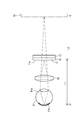
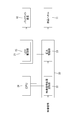
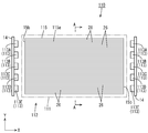
- FIG. 1 is a schematic perspective view showing a state in which a user wears a head mounted display according to Embodiment 1 of the present invention on a head.
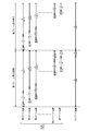
- Schematic side view showing an optical relationship between a liquid crystal display device and a lens unit included in a head-mounted device constituting a head-mounted display, and a user's eyeball Plan view of a backlight device constituting a liquid crystal display device Cross section of liquid crystal display Cross section of LED and LED board Block diagram regarding control of liquid crystal panel and backlight device
- a goggle-type head-mounted display (HMD) HMD and a liquid crystal display device (display device) 10 used therein are exemplified.
- a part of each drawing shows an X axis, a Y axis, and a Z axis, and each axis direction is drawn to be a direction shown in each drawing.
- the goggle-type head-mounted display HMD includes a head-mounted device HMDa that is mounted so as to surround both eyes in the user's head HD.
- the head-mounted device HMDa includes a liquid crystal display device 10 that displays an image, and a lens unit that forms an image displayed on the liquid crystal display device 10 on a user's eyeball (eye) EY. At least a built-in eyepiece unit RE).
- the liquid crystal display device 10 includes at least a liquid crystal panel (display panel) 11 and a backlight device (illumination device) 12 that irradiates the liquid crystal panel 11 with light.
- the lens unit RE is disposed between the liquid crystal display device 10 and the user's eyeball EY, and imparts a refractive action to the transmitted light.
- the focal length of the lens unit RE By adjusting the focal length of the lens unit RE, the image formed on the retina (eye) EYb via the crystalline lens EYa of the eyeball EY is smaller than the actual distance L1 from the eyeball EY to the liquid crystal display device 10.
- the user can be made to recognize it as displayed on the virtual display VD that is apparently present at the position of the far distance L2.
- the user can display on the virtual display VD having a screen size (for example, about several tens of inches to several hundred inches) that is much larger than the screen size of the liquid crystal display device 10 (for example, about 0.
- the enlarged image (virtual image) is visually recognized.
- the liquid crystal display device 10 is mounted on the head-mounted device HMDa and display the right-eye image and the left-eye image on the liquid crystal display device 10
- the liquid crystal display device 10 is displayed on the head-mounted device HMDa. It is also possible to display the right-eye image on one liquid crystal display device 10 and the left-eye image on the other liquid crystal display device 10.
- illustration is abbreviate
- the liquid crystal panel 11 and the backlight device 12 constituting the liquid crystal display device 10 will be described sequentially.
- the plate surface on the lens unit RE side is a display surface 11a for displaying an image.
- the liquid crystal panel 11 has a rectangular plate shape as a whole, and is sealed between a pair of glass substrates bonded together with a predetermined gap therebetween, and both glass substrates.
- One glass substrate array substrate, active matrix substrate
- switching elements for example, TFTs
- the pixel electrodes arranged in the region and connected to the switching element are arranged in a matrix (matrix) in a plane, and an alignment film and the like are provided.
- the other glass substrate (counter substrate, CF substrate) is provided with three color filters exhibiting R (red), G (green), and B (blue) arranged in a matrix in a predetermined arrangement.
- a light shielding layer black matrix having a substantially lattice shape, a solid counter electrode opposing the pixel electrode, an alignment film, and the like are provided so as to be arranged between adjacent color filters.
- R, G, and B color filters arranged in the X-axis direction (row direction, gate wiring extending direction) and three pixel electrodes facing each color filter have three colors. These three pixels constitute display pixels capable of color display with a predetermined gradation.
- a large number of pixels are arranged along the X-axis direction to form one pixel group, and this pixel group is arranged in a large number along the Y-axis direction (column direction).
- a large number of pixels are arranged in a matrix on the display surface 11a of the liquid crystal panel 11.
- the gate wiring described above extends along the X-axis direction, which is the arrangement direction of a large number of pixels constituting the pixel group, and collectively drives switching elements connected to the large number of pixels constituting the pixel group.
- a large number of gate wirings are individually connected to a large number of pixel groups arranged along the Y-axis direction, and along the Y-axis direction based on a signal supplied from a control board (not shown). It is possible to sequentially scan a large number of arranged pixel groups.
- the number of pixel groups arranged (number of scans) is, for example, “1080” when the liquid crystal panel 11 has 2K resolution, and “2160” when the liquid crystal panel 11 has 4K resolution.
- polarizing plates are arranged on the outer sides of both glass substrates.
- the external shape of the liquid crystal panel 11 is shown with the dashed-two dotted line.
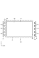
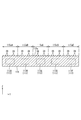
- the backlight device 12 has a horizontally long rectangular shape as a whole, and includes an LED (light source) 13, an LED substrate (light source substrate) 14 on which the LED 13 is mounted, and the LED 13. At least a light guide plate 15 that guides the light and an optical sheet (optical member) 16 that is stacked on the front side of the light guide plate 15.
- the backlight device 12 is a double-sided light input type edge light type (side light type) in which light from the LED 13 enters the light guide plate 15 from both sides.
- the long side direction coincides with the X-axis direction in each drawing
- the short side direction coincides with the Y-axis direction
- the thickness direction coincides with the Z-axis direction.
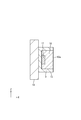
- the LED 13 is a so-called top surface emitting type in which the LED 13 is surface-mounted and the light emitting surface 13a faces away from the LED substrate 14 side.
- the LED 13 includes a blue LED element (blue light emitting element, blue LED chip) 17 that is a light source, a sealing material 18 that seals the blue LED element 17, and a blue LED element 17. And a case (housing body, housing) 19 filled with the sealing material 18.
- the blue LED element 17 is a semiconductor made of a semiconductor material such as InGaN, and emits blue light having a wavelength included in a blue wavelength region (about 420 nm to about 500 nm) when a voltage is applied in the forward direction.
- the main emission wavelength of the blue LED element 17 is preferably about 450 nm, but this is not necessarily the case.
- the sealing material 18 has a configuration in which a green phosphor and a red phosphor, both of which are not shown, are dispersed and blended at a predetermined ratio in a substantially transparent thermosetting resin material (for example, an epoxy resin material). .
- the green phosphor emits green light having a wavelength included in the green wavelength region (about 500 nm to about 570 nm) by being excited by blue light emitted from the blue LED element 17.
- the green phosphor is, for example, ⁇ -SiAlON, which is a kind of sialon phosphor, and the main emission wavelength is preferably about 540 nm, but this is not necessarily limited.
- the red phosphor emits red light having a wavelength included in a red wavelength region (about 600 nm to about 780 nm) by being excited by blue light emitted from the blue LED element 17. Details of the red phosphor will be described later in detail. Therefore, the light emitted from the LED 13 includes blue light (blue component light) emitted from the blue LED element 17, green light (green component light) emitted from the green phosphor, and red light emitted from the red phosphor. (Red component light), and generally white as a whole.
- the case 19 has a substantially box shape having an opening on the light emission side (light emission surface 13a side) as a whole, and the blue LED element 17 and the sealing material 18 are accommodated therein.
- the LED substrate 14 has a long plate shape extending along the Y-axis direction (the short side direction of the backlight device 12) and faces the light guide plate 15 side.
- a plurality of (five in FIG. 3) LEDs 13 are mounted on the plate surface at substantially equal intervals along the Y-axis direction.
- the LED boards 14 are arranged in a pair at a position sandwiching the light guide plate 15 in the X-axis direction (long side direction of the backlight device 12).
- a wiring pattern (not shown) for connecting a plurality of LEDs 13 in series is formed on the mounting surface of the LED 13 on the LED substrate 14, and the other end side of a wiring member whose one end side is connected to an external LED drive circuit board is connected A connector portion (not shown together with the wiring member) is provided.
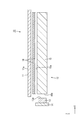
- the light guide plate 15 is made of a synthetic resin material (for example, acrylic resin such as PMMA) having a refractive index sufficiently higher than air and substantially transparent. As shown in FIGS. 3 and 4, the light guide plate 15 has a flat plate shape, and the plate surface thereof is parallel to the plate surface (display surface 11 a) of the liquid crystal panel 11. Of the pair of plate surfaces of the light guide plate 15, the plate surface on the front side and disposed opposite to the liquid crystal panel 11 and the optical sheet 16 is a light output plate surface 15 a that emits light guided inside.
- the light guide plate 15 is disposed immediately below the liquid crystal panel 11 and the optical sheet 16, and the end surfaces on the pair of short sides of the outer peripheral end surfaces thereof are the mounting surfaces of the pair of LED substrates 14 and the respective mounting surfaces thereof.
- the light emitting surface 13a of the LED 13 is opposed to a pair of light incident end surfaces 15b on which light from the light emitting surface 13a is incident.
- the light guide plate 15 introduces light emitted from each LED 13 toward the light guide plate 15 along the X-axis direction (the alignment direction of the LEDs 13 and the light guide plate 15) from the pair of light incident end surfaces 15b, and After propagating the light inside, the light is raised to the optical sheet 16 side (front side, light emitting side) along the Z-axis direction (the alignment direction of the liquid crystal panel 11 and the optical sheet 16 and the light guide plate 15). It has a function of emitting light from the optical plate surface 15a.
- the optical sheet 16 is disposed so as to be interposed between the liquid crystal panel 11 and the light guide plate 15, thereby transmitting the light emitted from the light guide plate 15 and providing a predetermined amount of light to the transmitted light.
- the light is emitted toward the liquid crystal panel 11 while providing an optical action.
- the optical sheet 16 includes a plurality of sheets (two sheets in the present embodiment), and specific types thereof include, for example, a diffusion sheet, a lens sheet (prism sheet), a reflective polarizing sheet, and the like. It is possible to select and use as appropriate.
- the liquid crystal display device 10 includes a panel control unit 20 for controlling the driving of the liquid crystal panel 11 and a backlight control unit for controlling the driving of the backlight device 12 ( Lighting control unit) 21.
- the panel control unit 20 includes a video signal processing circuit unit 22 that processes a video signal, and a pixel driving unit 23 that drives each pixel based on an output signal from the video signal processing circuit unit 22. Is provided.
- the control board is provided with a CPU 24 for controlling operations of the video signal processing circuit unit 22, the pixel driving unit 23, and an LED driving unit 25 described later.
- the backlight control unit 21 includes an LED driving unit 25 that drives the LED 13 based on an output signal from the video signal processing circuit unit 22 and is provided on the LED driving circuit board.
- the operation of the LED drive unit 25 is controlled by the CPU 24 of the control board, and is synchronized with the operation of the pixel drive unit 23.
- the panel control unit 20 changes a number of pixel groups arranged along the Y-axis direction by the pixel driving unit 23 from a pixel group located at one end to a pixel group located at the other end.
- the scanning signal is sequentially supplied to a large number of gate wirings arranged along the Y-axis direction, and to the large number of source wirings arranged along the X-axis direction.
- the image signals are supplied respectively.
- the one located at one end (upper end in the vertical direction) in the Y-axis direction is referred to as a “first gate wiring”, and then the Y-axis “Second gate wiring” and “third gate wiring” are sequentially set toward the other end in the direction, and “nth gate wiring” is located at the other end (the lower end in the vertical direction) in the Y-axis direction.
- first gate wiring the one located at one end (upper end in the vertical direction) in the Y-axis direction
- nth gate wiring is located at the other end (the lower end in the vertical direction) in the Y-axis direction.
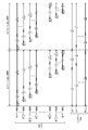
- the total scanning period for all the pixel groups is the total number of gate wirings (pixel groups). Divided number.
- the unit scanning period T1 is about 7.72 ⁇ sec (microseconds) when the liquid crystal panel 11 has 2K resolution, and in the case of 4K resolution. It is set to about 3.86 ⁇ sec.
- the time required for the orientation change of the liquid crystal layer is set as a liquid crystal response time T2 ("LC" is also written in FIG. 7), and specifically, for example, about 4 msec in this embodiment.
- T2 liquid crystal response time
- each pixel included in the pixel group transmits light supplied from the backlight device 12 described below to the second alignment state of the liquid crystal molecules.
- the light is transmitted with the transmittance based on the above, and the display is performed with a predetermined gradation.
- the holding period T3 in which the second alignment state of the liquid crystal molecules is held in each pixel constituting the pixel group (also shown as “HOLD” in FIG.
- the backlight control unit 21 includes a light-off period T ⁇ b> 4 (“OFF” is also shown in FIG. 7) and a light-up period in one frame display period in the liquid crystal panel 11 whose driving is controlled by the panel control unit 20.
- the drive of each LED 13 is controlled so that T5 ("ON" is also written in FIG. 7) is included.
- the backlight control unit 21 starts the extinguishing period T4 in synchronization with the start of the one-frame display period, starts the lighting period T5 after the extinguishing period T4 ends, and ends the one-frame display period.
- the driving of each LED 13 is controlled so that the lighting period T5 ends in synchronization with the above.
- the plurality of LEDs 13 mounted on the pair of LED boards 14 are collectively controlled by the backlight control unit 21 so that the turn-off period T4 and the turn-on period T5 are the same.
- the lighting period T5 is, for example, about 1 msec.
- the turn-off period T4 is a value obtained by subtracting the turn-on period T5 from the one-frame display period, and specifically, for example, about 12.33 msec. That is, the LED 13 is turned on only for a short time before the end of the one frame display period, and is turned off at other times.
- the LED 13 is driven by a so-called impulse type by the backlight control unit 21, so that when the moving image is displayed on the liquid crystal panel 11, the afterimage is more difficult to be visually recognized by the user, and the moving image display performance is further improved. It will be excellent.
- the concrete numerical value of the light extinction period T4 and the lighting period T5 can be changed suitably.
- the red phosphor of the LED 13 includes at least a double fluoride red phosphor.
- the double fluoride red phosphor is a fluoride complex red phosphor using manganese as an activator. Specifically, for example, K 2 SiF 6 (hereinafter referred to as “KSF phosphor”) is used. .
- KSF phosphor is characterized in that the main emission wavelength is about 630 nm, for example, and both the color reproducibility and luminance related to the emitted red light are high.
- the KSF phosphor has a characteristic of continuously emitting red light for a predetermined time after the supply of blue light as excitation light from the blue LED element 17 is interrupted. There is concern about degrading the quality.
- the red phosphor of the LED 13 according to this embodiment includes a nitride red phosphor mixed with a double fluoride red phosphor.
- the nitride-based red phosphor is an alkaline earth silico-nitride red phosphor using europium as an activator. Specifically, for example, CaAlSiN 3 (hereinafter referred to as “CASN phosphor”) is used. It is done.
- the CASN phosphor has a main emission wavelength of, for example, about 650 nm, and has a color reproducibility and luminance related to the emitted red light that is lower than that of the KSF phosphor, but the afterglow time is much longer than that of the KSF phosphor. It is short, for example, about 1/100 to 1/1000.
- what mixed KSF fluorescent substance and CASN fluorescent substance with each predetermined content ratio is used for the red fluorescent substance of LED13, and the content ratio of KSF fluorescent substance is specifically 50%. While the above range is 85% or less, the CASN phosphor content ratio is 15% or more and 50% or less. According to such a configuration, the red light is difficult to be visually recognized as afterglow, while the color reproducibility and luminance related to red light are excellent. Specifically, when the content ratio of the KSF phosphor is 50% or more, or when the content ratio of the CASN phosphor is 50% or less, the content ratio of the KSF phosphor is temporarily smaller than 50%.
- the color reproducibility and the luminance relating to the red light can be maintained sufficiently high. Furthermore, when the content ratio of the KSF phosphor is 85% or less, or when the content ratio of the CASN phosphor is 15% or more, the content ratio of the KSF phosphor is temporarily larger than 85%. Compared with the case where the content ratio of the CASN phosphor is less than 15%, the afterglow of red light is less visible.
- the liquid crystal display device 10 is provided in the head-mounted device HMDa constituting the head mounted display HMD, the afterglow of red light becomes difficult to be visually recognized as described above, so that the user's operation This is suitable for displaying an image following the above without delay, and is excellent in display quality, and is less likely to cause discomfort called “VR sickness” to the user.
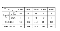
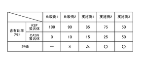
- the LED 13 was used in Example 2, and the LED 13 in which the content ratio of the KSF phosphor was 50% and the content ratio of the CASN phosphor was 50% was used as Example 3.
- the LED of Comparative Example 1 does not contain a CASN phosphor.
- the LEDs according to Comparative Examples 1 and 2 and Examples 1 to 3 are different from each other in the composition of the red phosphor, but the total amount of the red phosphor contained in the sealing material is the same, and the red phosphor It is the same also about structures (blue LED element, green fluorescent substance, etc.) other than a body.
- the LEDs according to Comparative Examples 1 and 2 and Examples 1 to 3 were applied to the liquid crystal display device 10 shown in FIGS. 3 and 4, and each LED was turned on.
- the luminance and chromaticity of the display surface 11a of the liquid crystal panel 11 were measured. The result is shown in FIG.
- the relative luminance (unit: “%”) described in FIG. 8 is a relative value when the luminance value of the display surface 11a of the liquid crystal panel 11 is 100% when the LED of Comparative Example 1 is used.
- the relative NTSC ratio (unit: “%”) described in FIG. 8 is a relative value when the NTSC ratio of the liquid crystal panel 11 is 100% when the LED of Comparative Example 1 is used.
- the NTSC ratio is a ratio based on the NTSC chromaticity region according to the NTSC (National Television System Standardization Committee) standard (100%), and the area value of the chromaticity region obtained by measurement Is a ratio obtained by dividing by the area value of the NTSC chromaticity region.
- the color reproducibility and brightness are sufficiently high.
- the content ratio of the CASN phosphor is larger than 50%, the contribution of the KSF phosphor is weakened, and it is considered that both the relative luminance and the relative NTSC ratio are decreased.
- the lower limit value of the content ratio of the KSF phosphor is preferably 50%
- the upper limit value of the content ratio of the CASN phosphor is preferably 50%.
- the content ratio of the KSF phosphor is secured to 75% or more as in Example 2
- the relative luminance is secured to 93.4% or more
- the relative NTSC ratio is secured to 94.6% or more. It can be said that reproducibility and brightness are higher. Therefore, in order to ensure higher color reproducibility and luminance, it is preferable that the content ratio of the KSF phosphor is 75% or more and the content ratio of the CASN phosphor is 25% or less.
- the evaluation is considered to be x (impossible).
- the CASN phosphor has a content ratio of 15% as in Example 1, it seems that the afterglow time of red light is further shortened and is close to the LED lighting period T5. As a result, it is difficult for the user to visually recognize the afterglow of red light, the display quality is improved, and the evaluation is considered to be ⁇ (possible).
- the CASN phosphor has a content ratio of 25% as in Example 2
- the CASN phosphor has a content ratio of 50% as in Example 3
- the residual red light remains.
- the light time is considered to be extremely short, and is considered to be shorter than the LED lighting period T5 and the liquid crystal response period T2.
- the content ratio of CASN phosphor is set to 25% and the content ratio of KSF phosphor is set to 75%. More preferably.
- the liquid crystal display device (display device) 10 includes the liquid crystal panel (display panel) 11 that can display an image, and the backlight device (illumination) that supplies light for display to the liquid crystal panel 11.
- the backlight control unit 21 that controls the driving of the LED 13 so as to include the lighting period T5 and the extinguishing period T4 in the display period, and a red phosphor are configured.
- a double fluoride red phosphor having a content ratio in the range of 50% or more and 85% or less, and a nitride system constituting the red phosphor and having a content ratio in the range of 15% or more and 50% or less
- a red phosphor A double fluoride red phosphor having a content ratio in the range of 50% or more and 85% or less, and a nitride system constituting the red phosphor and having a content ratio in the range of 15% or more and 50% or less.
- the liquid crystal panel 11 is supplied with light from the backlight device 12 from the backlight device 12 in which the drive of the LED 13 is controlled by the backlight control unit 21, and this light is used. Then, an image is displayed on the liquid crystal panel 11.
- the LED 13 of the backlight device 12 has at least a blue light emitted from the blue LED element 17 and a red phosphor that emits red light when excited by the blue light from the blue LED element 17.
- the red phosphor contains a double fluoride red phosphor, which is excellent in color reproducibility and luminance relating to red light.
- the backlight control unit 21 controls the driving of the LED 13 in synchronization with the display on the liquid crystal panel 11. More specifically, the backlight control unit 21 controls the lighting period T 5 during one frame display period on the liquid crystal panel 11. The LED 13 including the turn-off period T4 is driven. As a result, for example, when displaying a moving image on the liquid crystal panel 11, it is difficult for the user to visually recognize the afterimage, and thus the moving image display performance is excellent. On the other hand, even when the LED 13 is switched from the on state to the off state by the backlight control unit 21, among the red phosphors that the LED 13 has, the double fluoride red phosphor is supplied with blue light from the blue LED element 17.
- the red phosphor contains a nitride-based red phosphor in addition to the double fluoride red phosphor, the red light has excellent color reproducibility and luminance relating to red light. Becomes difficult to be visually recognized as afterglow. Specifically, when the content ratio of the double fluoride red phosphor is 50% or more, or when the content ratio of the nitride red phosphor is 50% or less, the double fluoride red phosphor is temporarily assumed.
- the color reproducibility and luminance relating to red light can be maintained sufficiently high. it can. Furthermore, when the content ratio of the double fluoride red phosphor is 85% or less or when the content ratio of the nitride red phosphor is 15% or more, the double fluoride red phosphor is temporarily included. Compared with the case where the ratio is larger than 85% or the case where the content ratio of the nitride-based red phosphor is smaller than 15%, the afterglow of red light is less visible.
- the double fluoride red phosphor has a content ratio of 75% or more and 85% or less, whereas the nitride-based red phosphor has a content ratio of 15% or more and 25% or less. It is made the range. In this way, when the content ratio of the double fluoride red phosphor is 75% or more, or when the content ratio of the nitride red phosphor is 25% or less, the double fluoride red fluorescence is temporarily assumed. Maintain the color reproducibility and brightness of red light sufficiently higher than when the content ratio of the body is less than 75% or when the content ratio of the nitride-based red phosphor is greater than 25%. Can do.
- the double fluoride red phosphor is temporarily included. Compared with the case where the ratio is larger than 85% and the case where the content ratio of the nitride-based red phosphor is smaller than 15%, the afterglow of red light is less visible.
- the content ratio of the double fluoride red phosphor is 85%, whereas the content ratio of the nitride red phosphor is 15%. In this way, the color reproducibility and luminance relating to the red light can be made extremely high, and the afterglow of the red light is not easily visually recognized.
- the content ratio of the double fluoride red phosphor is 75%, whereas the content ratio of the nitride-based red phosphor is 25%. In this way, the afterglow of red light is reliably prevented from being visually recognized.
- the double fluoride red phosphor is a fluoride complex red phosphor using manganese as an activator. This is suitable for keeping the color reproducibility and luminance related to red light high.
- the nitride-based red phosphor is an alkaline earth silico-nitride red phosphor using europium as an activator. This is suitable for making it difficult to visually recognize the afterglow associated with red light.
- the backlight control unit 21 starts the turn-off period T4 in synchronization with the start of the one-frame display period, starts the turn-on period T5 after the turn-off period T4 ends, and synchronizes with the end of the one-frame display period. Then, the driving of the LED 13 is controlled so that the lighting period T5 ends.
- the LED 13 is driven by the backlight controller 21 by the impulse type, for example, when displaying a moving image on the liquid crystal panel 11, the afterimage is more difficult to be visually recognized by the user, and thus the moving image display performance is more excellent. It becomes.
- the head mounted display HMD includes the liquid crystal display device 10 described above, a lens unit RE that forms an image displayed on the liquid crystal display device 10 on a user's eyeball (eye) EY, and a liquid crystal display.
- the head mounting device HMDa that includes the display device 10 and the lens unit RE and is mounted on the user's head HD is provided.
- the head mounted display HMD having such a configuration, when the user uses the head-mounted device HMDa mounted on the head HD, the image displayed on the liquid crystal display device 10 is displayed on the user by the lens unit RE. The image is formed on the eyeball EY, so that the user can visually recognize the image displayed on the liquid crystal display device 10 in an enlarged form.
- liquid crystal display device 10 provided in the head-mounted device HMDa is difficult to visually recognize the afterglow of red light, it is suitable for displaying an image following the operation of the user without delay, and is excellent in display quality. At the same time, the user is less likely to experience discomfort called “VR sickness”.
- Embodiment 2 A second embodiment of the present invention will be described with reference to FIGS. In this Embodiment 2, what changed the structure and control of the backlight apparatus 112 is shown. In addition, the overlapping description about the same structure, operation
- the light guide plate 115 constituting the backlight device 112 is provided with a prism (directional light guide) 26 on the light output plate surface 115a.
- the prism 26 has a mountain shape with a substantially triangular (substantially right-angled triangle) cross-sectional shape, and is a protrusion that extends linearly along the X-axis direction (the normal direction of the light emitting surface 113a of the LED 113).
- a plurality of light emitting plate surfaces 115a are arranged side by side along the Y-axis direction in the plane of the light output plate surface 115a.
- the prism 26 Since the prism 26 has an apex angle set substantially at right angles, the light propagating through the light guide plate 115 and totally reflected at the interface of the prism 26 has a Y-axis direction (alignment of the LEDs 113) in the light guide plate 115.
- directivity is provided so as to travel substantially straight along the X-axis direction. That is, the prism 26 imparts directivity that restricts light introduced from the LED 113 into the light guide plate 115 from diffusing in the Y-axis direction.
- the light exit plate surface 115a of the light guide plate 115 is divided into five horizontally long belt-like regions that are the same as the number of LEDs 113 arranged, and these five divided regions are selectively selected according to the lighting of the five LEDs 113. Flashes.
- the five LEDs 113 arranged in the Y-axis direction are referred to as a first LED 113A, a second LED 113B, a third LED 113C, a fourth LED 113D, and a fifth LED 113E in order from the top shown in FIG. 10 (left side shown in FIG. 11). Accordingly, the light of the first divided region 115aA and the second LED 113B that emits the light of the first LED 113A in the five divided regions on the light output plate surface 115a of the light guide plate 115 from the top shown in FIG. 10 (left side shown in FIG. 11).
- the second partitioned region 115aB that emits the light the third partitioned region 115aC that emits the light of the third LED 113C, the fourth partitioned region 115aD that emits the light of the fourth LED 113D, and the fifth partitioned region 115aE that emits the light of the fifth LED 113E.
- the light emitted from each of the divided regions 115aA to 115aE on the light exit plate surface 115a of the light guide plate 115 is a specific plurality of pixel groups among a large number of pixel groups included in the liquid crystal panel 111. Will be selectively supplied. That is, the large number of pixel groups provided in the liquid crystal panel 111 includes a first pixel group including a plurality of pixel groups that are overlapped with the first segmented region 115aA and selectively supplied with light from the first segmented region 115aA.
- a second pixel group consisting of a plurality of pixel groups that are selectively supplied with light from the second segmented region 115aB and superimposed on the second segmented region 115aB, and a third segmented region 115aC superimposed on the third segmented region 115aC.
- a third pixel group consisting of a plurality of pixel groups to which light of a predetermined amount is supplied and from a plurality of pixel groups to which light from the fourth partitioned region 115aD is selectively supplied in an overlapping manner with the fourth partitioned region 115aD
- a fifth pixel group composed of a plurality of pixel groups that are selectively supplied with light from the fifth segmented region 115aE so as to overlap the fifth segmented region 115aE.
- the total number of gate wirings is n, and the one located at one end in the Y-axis direction is referred to as the “first gate wiring” and is located at the other end in the Y-axis direction.
- the first pixel group is scanned by the (n / 5) th gate wiring from the first gate wiring, and the second pixel group is scanned by the (n / 5 + 1) th gate wiring.
- the third pixel group is scanned from the (2n / 5 + 1) gate wiring to the (3n / 5) gate wiring, and the fourth pixel group is scanned to the (3n / 5th) gate wiring.
- the 5 + 1) gate wiring is scanned by the (4n / 5) gate wiring
- the fifth pixel group is scanned by the (4n / 5 + 1) gate wiring by the nth gate wiring.
- a plurality of pixel groups are sequentially scanned by a panel control unit (both backlight control units are not shown in this embodiment, but refer to FIG. 6).
- the driving of the plurality of LEDs 113 is controlled in synchronism with the driving of the pixel group to be supplied with light so that the extinguishing period T4 and the lighting period T5 are included while being driven.
- the second alignment state of the liquid crystal molecules is maintained as the plurality of pixel groups constituting the first pixel group are scanned and driven by the (n / 5) th gate line from the first gate line.
- the first LED 113A of the backlight device 112 is in the extinguishing period T4 until reaching the holding period T3, and after a predetermined time has elapsed since reaching the holding period T3, the first LED 113A shifts to the lighting period T5.
- the second LED 113B of the backlight device 112 is set to the extinguishing period T4, and after a predetermined time has elapsed since reaching the holding period T3, the second LED 113B shifts to the lighting period T5.
- the lighting period T5 of the second LED 113B is started later than the lighting period T5 of the first LED 113A.
- the timing of the turn-off period T4 and the turn-on period T5 of the third LED 113C, the fourth LED 113D, and the fifth LED 113E is also determined in synchronization with the scanning and driving of the third pixel group, the fourth pixel group, and the fifth pixel group in the same manner as described above. .
- the lighting periods T5 of the LEDs 113A to 113E are all equal, and a part thereof extends over the first frame display period and the second frame display period.
- the backlight control unit controls the driving of the LEDs 113A to 113E in synchronization with the scanning of the pixel groups by the panel control unit, so that an afterimage is displayed to the user when displaying a moving image on the liquid crystal panel 111. It becomes harder to see, and the moving image display performance becomes better.
- the red phosphor of the LED 113 is a mixture of a KSF phosphor and a CASN phosphor, and the content ratio of the KSF phosphor is 50% or more and 85% or less.
- the content ratio of the CASN phosphor is 15% or more and 50% or less, sufficient color reproducibility and luminance of red light can be obtained, and afterglow of red light is suppressed.
- the panel control unit (see FIG. 6) that controls the driving of the liquid crystal panel 111 is provided, and the liquid crystal panel 111 includes a plurality of pixels arranged in a matrix.
- the panel control unit sequentially scans a pixel group including a plurality of pixels arranged in the row direction along the column direction during one frame display period, and the backlight device 112 includes a plurality of pixels.
- the plurality of LEDs 113 are arranged so as to selectively supply light to a plurality of pixel groups, and the backlight control unit (see FIG. 6) controls the plurality of pixel groups.
- the plurality of LEDs 113 are driven in synchronism with the driving of the pixel group to be supplied with light so that the lighting period T5 and the extinguishing period T4 are included while being sequentially driven by the scanning unit. Control .
- the backlight controller controls the driving of the LED 113 in synchronization with the scanning of the plurality of pixel groups by the panel controller, for example, when displaying a moving image on the liquid crystal panel 111, the afterimage is more visually recognized by the user. As a result, the moving image display performance is improved.
- the KSNAF phosphor K 2 Si 1-x Na x Al x F 6 : Mn
- KTF phosphor K 2 TiF 6 : Mn
- the red phosphor is composed of only two types of KSF phosphor and CASN phosphor.
- another red phosphor is included in the KSF phosphor and CASN phosphor. It is also possible to use three or more types.
- the red phosphor to be added is preferably a double fluoride red phosphor or a nitride red phosphor, but this is not necessarily the case.
- the material of the blue LED element and the green phosphor constituting the LED, the green phosphor, the main emission wavelength, and the like can be appropriately changed.
- a yellow phosphor can be included in the sealing material.
- the pair of LED substrates (LEDs) is disposed in a form facing the pair of short-side end surfaces of the light guide plate.
- a pair of LED substrates (LEDs) may be arranged so as to face the pair of long side end faces of the light guide plate.
- the LED substrate (LED) may be arranged in a form facing only one end surface on the short side or the long side of the outer peripheral end surface of the light guide plate.
- the arrangement and the number of LED substrates (LEDs) with respect to the outer peripheral end surface of the light guide plate can be appropriately changed.
- the backlight control unit is provided on the LED drive circuit board.
- the LED drive circuit board may be omitted and the backlight control unit may be provided on the control board. I do not care.
- the liquid crystal display device including the liquid crystal panel is illustrated, but other types of display panels (PDP (plasma display panel), organic EL panel, EPD (electrophoretic display panel), MEMS ( The present invention can also be applied to a display device equipped with a display panel (Micro Electro Mechanical Systems).
- PDP plasma display panel
- EPD electrostatic display panel
- MEMS MEMS
- the present invention can also be applied to a display device equipped with a display panel (Micro Electro Mechanical Systems).
- a head-mounted display is shown. However, the present invention is applied to a head-up display, a projector, and the like as a device that enlarges and displays an image displayed on a liquid crystal panel using a lens or the like. Applicable.
- the present invention is also applicable to liquid crystal display devices that do not have an enlarged display function (such as a television receiver, a tablet terminal, and a smartphone).
- the planar shape of the liquid crystal display device (liquid crystal panel or backlight device) is a horizontally long rectangle is shown.
- the planar shape of the liquid crystal display device is a square, an octagon, or the like. It may be a pentagon or more polygon, a vertically long rectangle, a circle, a semicircle, an oval, an ellipse, a trapezoid, or the like.
- the top-emitting LED is shown, but a side-emitting LED can be used as the light source.
- the case where the light-emitting plate surface of the light guide plate is made flat has been shown.
- a lenticular lens portion made of a protrusion having a semicircular cross section (saddle shape).
- the reflective dots scatter and reflect light propagating in the light guide plate to promote light output from the light output plate surface, and the distribution pattern makes the luminance distribution related to the light emitted from the light output plate surface uniform. It has been adjusted.
- the structure which concerns on a light-guide plate can be changed suitably.
Abstract
A liquid crystal display apparatus 10 is provided with: a liquid crystal panel 11; a backlight device 12; an LED 13 having at least a blue LED element 17 for emitting blue light and a red phosphor for emitting red light by excitation thereof with blue light from the blue LED element 17; a backlight control unit 21 for controlling driving of the LED 13 in synchrony with display by the liquid crystal panel 11, the backlight control unit 21 controlling driving of the LED 13 so that a light-on period and a light-off period are included in a single-frame display period in the liquid crystal panel 11; a complex fluoride red phosphor constituting part of the red phosphor and being in a content ratio range of 50% to 85%; and a nitride-based red phosphor constituting part of the red phosphor and being in a content range of 15% to 50%.
Description
本発明は、表示装置及びヘッドマウントディスプレイに関する。
The present invention relates to a display device and a head mounted display.
従来、液晶表示装置の一例として下記特許文献1に記載されたものが知られている。特許文献1に記載された液晶表示装置に備わる制御回路の光源制御部は、ゲートドライバ制御部からゲートドライバに出力されるラッチパルス信号に同期して、各光源電源回路に対して発光制御信号を出力する。各光源電源回路は、入力された発光制御信号に基づき、冷陰極管の発光状態を第1乃至第3のいずれかの発光状態に切り替えて、LCDパネルを表示領域裏面から照明する。第1段階の発光状態は消灯状態であり、第2段階の発光状態は最大点灯輝度が得られる最大点灯状態であり、第3の発光状態は第2段階の発光状態のほぼ半分の輝度が得られる中間点灯状態である。
Conventionally, what was described in following patent document 1 is known as an example of a liquid crystal display device. The light source control unit of the control circuit included in the liquid crystal display device described in Patent Document 1 outputs a light emission control signal to each light source power supply circuit in synchronization with the latch pulse signal output from the gate driver control unit to the gate driver. Output. Each light source power circuit illuminates the LCD panel from the rear surface of the display area by switching the light emission state of the cold cathode tube to any one of the first to third light emission states based on the input light emission control signal. The light emission state in the first stage is a light-off state, the light emission state in the second stage is a maximum light-on state in which the maximum lighting brightness can be obtained, and the third light-emitting state has a brightness approximately half that of the light-emitting state in the second stage. The intermediate lighting state.
(発明が解決しようとする課題)
上記した特許文献1に記載されたような液晶表示装置では、光源制御部が冷陰極管を大電流で駆動した直後に電流を大きく低下させた後に滑らかに電流を増加させることで、冷陰極管に含まれる緑色蛍光体の残光を打ち消すようにしている。しかしながら、光源をLEDに変更し、それに伴って蛍光体の種類が変更された場合には、上記のようなduty駆動方法では蛍光体の残光を十分に打ち消すことができなくなるおそれがあり、また蛍光体が発する光に係る色再現性及び輝度が不十分になるおそれもある。 (Problems to be solved by the invention)
In the liquid crystal display device described inPatent Document 1 described above, the light source control unit greatly increases the current immediately after driving the cold cathode tube with a large current, and then increases the current smoothly, thereby reducing the cold cathode tube. The afterglow of the green phosphor contained in is canceled out. However, when the light source is changed to LED and the type of phosphor is changed accordingly, there is a possibility that the afterglow of the phosphor cannot be sufficiently canceled by the duty driving method as described above. There is also a possibility that the color reproducibility and the luminance related to the light emitted from the phosphor are insufficient.
上記した特許文献1に記載されたような液晶表示装置では、光源制御部が冷陰極管を大電流で駆動した直後に電流を大きく低下させた後に滑らかに電流を増加させることで、冷陰極管に含まれる緑色蛍光体の残光を打ち消すようにしている。しかしながら、光源をLEDに変更し、それに伴って蛍光体の種類が変更された場合には、上記のようなduty駆動方法では蛍光体の残光を十分に打ち消すことができなくなるおそれがあり、また蛍光体が発する光に係る色再現性及び輝度が不十分になるおそれもある。 (Problems to be solved by the invention)
In the liquid crystal display device described in
本発明は上記のような事情に基づいて完成されたものであって、赤色光の色再現性及び輝度を十分に得るとともに、赤色光の残光を抑制することを目的とする。
The present invention has been completed based on the above-described circumstances, and aims to sufficiently obtain the color reproducibility and luminance of red light and to suppress the afterglow of red light.
(課題を解決するための手段)
本発明の表示装置は、画像を表示可能な表示パネルと、前記表示パネルに表示のための光を供給する照明装置と、前記照明装置に備えられる光源であって、青色光を発光する青色発光素子と、前記青色発光素子からの青色光に励起されて赤色光を発光する赤色蛍光体と、を少なくとも有する光源と、前記表示パネルの表示に同期して前記光源の駆動を制御する照明制御部であって、前記表示パネルにおける1フレーム表示期間に点灯期間と消灯期間とが含まれるよう前記光源の駆動を制御する照明制御部と、前記赤色蛍光体を構成し、その含有比率が50%以上で且つ85%以下の範囲とされる複フッ化物赤色蛍光体と、前記赤色蛍光体を構成し、その含有比率が15%以上で且つ50%以下の範囲とされる窒化物系赤色蛍光体と、を備える。 (Means for solving the problem)
A display device according to the present invention includes a display panel capable of displaying an image, an illumination device that supplies light for display to the display panel, and a light source provided in the illumination device, and emitting blue light. A light source having at least an element, a red phosphor that emits red light when excited by blue light from the blue light emitting element, and an illumination control unit that controls driving of the light source in synchronization with display on the display panel The lighting control unit that controls the driving of the light source so that a one-frame display period in the display panel includes a lighting period and a non-lighting period, and the red phosphor, and the content ratio is 50% or more And a double fluoride red phosphor that is in the range of 85% or less, and a nitride-based red phosphor that constitutes the red phosphor and that has a content ratio of 15% or more and 50% or less With
このようにすれば、表示パネルには、照明制御部により光源の駆動が制御される照明装置から光が供給されるようになっており、この光を利用して表示パネルに画像が表示される。照明装置の光源は、青色発光素子から発せられた青色光と、青色発光素子からの青色光に励起されて赤色光を発光する赤色蛍光体と、を少なくとも有しており、このうちの赤色蛍光体には、複フッ化物赤色蛍光体が含まれているので、赤色光に係る色再現性及び輝度が優れたものとなっている。
In this way, light is supplied to the display panel from the illumination device whose light source is controlled by the illumination control unit, and an image is displayed on the display panel using this light. . The light source of the illuminating device has at least a blue light emitted from the blue light emitting element and a red phosphor that emits red light when excited by the blue light from the blue light emitting element. Since the body contains a double fluoride red phosphor, the color reproducibility and luminance relating to red light are excellent.
ここで、照明制御部は、表示パネルの表示に同期して光源の駆動を制御しており、詳しくは照明制御部は、表示パネルにおける1フレーム表示期間に点灯期間と消灯期間とが含まれる光源を駆動している。これにより、例えば表示パネルに動画を表示する際に使用者に残像が視認され難くなり、もって動画表示性能が優れたものとなる。その一方、照明制御部により光源が点灯状態から消灯状態へと移行しても、光源が有する赤色蛍光体のうち複フッ化物赤色蛍光体は、青色発光素子からの青色光の供給が途絶えた後も所定時間、赤色光を発し続ける特性を有しているため、赤色光が残光として視認されることが懸念される。その点、赤色蛍光体には、複フッ化物赤色蛍光体に加えて窒化物系赤色蛍光体が含まれているので、赤色光に係る色再現性及び輝度を優れたものとしつつも、赤色光が残光として視認され難いものとなる。具体的には、複フッ化物赤色蛍光体の含有比率が50%以上とされる場合や窒化物系赤色蛍光体の含有比率が50%以下とされる場合には、仮に複フッ化物赤色蛍光体の含有比率を50%よりも小さくした場合や窒化物系赤色蛍光体の含有比率を50%よりも大きくした場合に比べると、赤色光に係る色再現性及び輝度を十分に高く維持することができる。さらには、複フッ化物赤色蛍光体の含有比率が85%以下とされる場合や窒化物系赤色蛍光体の含有比率が15%以上とされる場合には、仮に複フッ化物赤色蛍光体の含有比率を85%よりも大きくした場合や窒化物系赤色蛍光体の含有比率を15%よりも小さくした場合に比べると、赤色光の残光が視認され難くなる。
Here, the illumination control unit controls the driving of the light source in synchronization with the display on the display panel. Specifically, the illumination control unit is a light source including a lighting period and an extinguishing period in one frame display period on the display panel. Is driving. Thereby, for example, when displaying a moving image on the display panel, it is difficult for the user to visually recognize the afterimage, and the moving image display performance is excellent. On the other hand, even when the light source is switched from the on state to the off state by the illumination control unit, the double fluoride red phosphor among the red phosphors that the light source has is after the blue light supply from the blue light emitting element is interrupted. However, since it has a characteristic of continuously emitting red light for a predetermined time, there is a concern that red light is visually recognized as afterglow. In that respect, since the red phosphor contains a nitride-based red phosphor in addition to the double fluoride red phosphor, the red light has excellent color reproducibility and luminance relating to red light. Becomes difficult to be visually recognized as afterglow. Specifically, when the content ratio of the double fluoride red phosphor is 50% or more, or when the content ratio of the nitride red phosphor is 50% or less, the double fluoride red phosphor is temporarily assumed. As compared with the case where the content ratio is less than 50% or the content ratio of the nitride-based red phosphor is larger than 50%, the color reproducibility and luminance relating to red light can be maintained sufficiently high. it can. Furthermore, when the content ratio of the double fluoride red phosphor is 85% or less or when the content ratio of the nitride red phosphor is 15% or more, the double fluoride red phosphor is temporarily included. Compared with the case where the ratio is larger than 85% and the case where the content ratio of the nitride-based red phosphor is smaller than 15%, the afterglow of red light is less visible.
本発明の実施態様として、次の構成が好ましい。
(1)前記複フッ化物赤色蛍光体は、含有比率が75%以上で且つ85%以下となる範囲とされるのに対し、前記窒化物系赤色蛍光体は、含有比率が15%以上で且つ25%以下となる範囲とされる。このようにすれば、複フッ化物赤色蛍光体の含有比率が75%以上とされる場合や窒化物系赤色蛍光体の含有比率が25%以下とされる場合には、仮に複フッ化物赤色蛍光体の含有比率を75%よりも小さくした場合や窒化物系赤色蛍光体の含有比率を25%よりも大きくした場合に比べると、赤色光に係る色再現性及び輝度を十分に高く維持することができる。さらには、複フッ化物赤色蛍光体の含有比率が85%以下とされる場合や窒化物系赤色蛍光体の含有比率が15%以上とされる場合には、仮に複フッ化物赤色蛍光体の含有比率を85%よりも大きくした場合や窒化物系赤色蛍光体の含有比率を15%より小さくした場合に比べると、赤色光の残光が視認され難くなる。 The following configuration is preferable as an embodiment of the present invention.
(1) The double-fluoride red phosphor has a content ratio of 75% or more and 85% or less, whereas the nitride-based red phosphor has a content ratio of 15% or more and The range is 25% or less. In this way, when the content ratio of the double fluoride red phosphor is 75% or more, or when the content ratio of the nitride red phosphor is 25% or less, the double fluoride red fluorescence is temporarily assumed. Maintain the color reproducibility and brightness of red light sufficiently higher than when the content ratio of the body is less than 75% or when the content ratio of the nitride-based red phosphor is greater than 25%. Can do. Furthermore, when the content ratio of the double fluoride red phosphor is 85% or less or when the content ratio of the nitride red phosphor is 15% or more, the double fluoride red phosphor is temporarily included. Compared with the case where the ratio is larger than 85% and the case where the content ratio of the nitride-based red phosphor is smaller than 15%, the afterglow of red light is less visible.
(2)前記複フッ化物赤色蛍光体は、含有比率が85%とされるのに対し、前記窒化物系赤色蛍光体は、含有比率が15%とされる。このようにすれば、赤色光に係る色再現性及び輝度を極めて高くすることができるとともに、赤色光の残光が十分に視認され難くなる。
(2) The double-fluoride red phosphor has a content ratio of 85%, whereas the nitride-based red phosphor has a content ratio of 15%. In this way, the color reproducibility and luminance relating to the red light can be made extremely high, and the afterglow of the red light is not easily visually recognized.
(3)前記複フッ化物赤色蛍光体は、含有比率が75%とされるのに対し、前記窒化物系赤色蛍光体は、含有比率が25%とされる。このようにすれば、赤色光の残光が確実に視認され難くなる。
(3) The content ratio of the double fluoride red phosphor is 75%, whereas the content ratio of the nitride red phosphor is 25%. In this way, the afterglow of red light is reliably prevented from being visually recognized.
(4)前記複フッ化物赤色蛍光体は、付活剤としてマンガンを用いたフッ化物錯体赤色蛍光体とされる。このようにすれば、赤色光に係る色再現性及び輝度を高く保つ上で好適となる。
(4) The double fluoride red phosphor is a fluoride complex red phosphor using manganese as an activator. This is suitable for keeping the color reproducibility and luminance related to red light high.
(5)前記窒化物系赤色蛍光体は、付活剤としてユーロピウムを用いたアルカリ土類ケイ窒化物赤色蛍光体とされる。このようにすれば、赤色光に係る残光を視認し難くする上で好適となる。
(5) The nitride red phosphor is an alkaline earth siliconitride red phosphor using europium as an activator. This is suitable for making it difficult to visually recognize the afterglow associated with red light.
(6)前記照明制御部は、前記1フレーム表示期間の開始に同期して前記消灯期間が開始され、前記消灯期間が終了された後に前記点灯期間が開始されて前記1フレーム表示期間の終了に同期して前記点灯期間が終了されるよう前記光源の駆動を制御する。このように照明制御部により光源の駆動がインパルス型となるから、例えば表示パネルに動画を表示する際に使用者に残像がより視認され難くなり、もって動画表示性能がより優れたものとなる。
(6) The illumination control unit starts the turn-off period in synchronization with the start of the one-frame display period, starts the turn-on period after the turn-off period ends, and ends the one-frame display period. The driving of the light source is controlled so that the lighting period ends in synchronization. As described above, since the illumination control unit drives the light source to be of an impulse type, for example, when displaying a moving image on the display panel, the afterimage is more difficult to be visually recognized by the user, and the moving image display performance is further improved.
(7)前記表示パネルの駆動を制御するパネル制御部を備えており、前記表示パネルは、行列状に並んで配される複数の画素を有するのに対し、前記パネル制御部は、前記1フレーム表示期間中に行方向に並んだ複数の前記画素からなる画素群を列方向に沿って順次に走査しており、前記照明装置は、複数の前記光源を有していてそれら複数の前記光源が複数の前記画素群に対して選択的に光を供給するよう配されており、前記照明制御部は、複数の前記画素群が前記パネル制御部により順次に走査されるのに伴って駆動されている間に前記点灯期間と前記消灯期間とが含まれるよう、光の供給対象となる前記画素群の駆動に同期する形で複数の前記光源の駆動を制御する。このように照明制御部により光源の駆動がパネル制御部による複数の画素群の走査に同期する形で制御されるから、例えば表示パネルに動画を表示する際に使用者に残像がより視認され難くなり、もって動画表示性能がより優れたものとなる。
(7) A panel control unit that controls driving of the display panel is provided. The display panel includes a plurality of pixels arranged in a matrix, whereas the panel control unit includes the one frame. A pixel group consisting of a plurality of the pixels arranged in the row direction during the display period is sequentially scanned along the column direction, and the illumination device includes the plurality of light sources, and the plurality of light sources are The lighting control unit is arranged to selectively supply light to the plurality of pixel groups, and the illumination control unit is driven as the plurality of pixel groups are sequentially scanned by the panel control unit. The driving of the plurality of light sources is controlled in synchronization with the driving of the pixel group to be supplied with light so that the lighting period and the extinguishing period are included. In this way, the illumination control unit controls the driving of the light source in synchronization with the scanning of the plurality of pixel groups by the panel control unit. For example, when displaying a moving image on the display panel, the afterimage is more difficult for the user to visually recognize. As a result, the moving image display performance is further improved.
次に、上記課題を解決するために、本発明のヘッドマウントディスプレイは、上記記載の表示装置と、前記表示装置に表示された画像を使用者の眼に結像させるレンズ部と、前記表示装置及び前記レンズ部を有していて前記使用者の頭部に装着される頭部装着器具と、を少なくとも備える。このような構成のヘッドマウントディスプレイによれば、使用者が頭部装着器具を頭部に装着した状態で使用すると、表示装置に表示された画像がレンズ部によって使用者の眼に結像し、もって使用者は表示装置に表示された画像を拡大した形で視認することが可能となる。頭部装着器具に備えられる表示装置は、赤色光の残光が視認され難くなっているので、使用者の動作に追従した画像を遅延なく表示する上で好適となり、表示品位に優れるとともに、使用者に「VR酔い」と呼ばれる不快感が生じ難いものとなる。
Next, in order to solve the above-described problem, a head-mounted display according to the present invention includes the display device described above, a lens unit that forms an image displayed on the display device on a user's eye, and the display device. And a head-mounted device that has the lens unit and is mounted on the head of the user. According to the head-mounted display having such a configuration, when the user uses the head-mounted device mounted on the head, the image displayed on the display device is formed on the user's eye by the lens unit, Accordingly, the user can visually recognize the image displayed on the display device in an enlarged form. Since the display device provided in the head-mounted device is difficult to visually recognize the afterglow of red light, it is suitable for displaying an image following the user's movement without delay, and has excellent display quality and use. It is difficult for a person to feel discomfort called “VR sickness”.
(発明の効果)
本発明によれば、赤色光の色再現性及び輝度を十分に得るとともに、赤色光の残光を抑制することができる。 (The invention's effect)
According to the present invention, sufficient color reproducibility and luminance of red light can be obtained, and afterglow of red light can be suppressed.
本発明によれば、赤色光の色再現性及び輝度を十分に得るとともに、赤色光の残光を抑制することができる。 (The invention's effect)
According to the present invention, sufficient color reproducibility and luminance of red light can be obtained, and afterglow of red light can be suppressed.
<実施形態1>
本発明の実施形態1を図1から図9によって説明する。本実施形態では、ゴーグル型のヘッドマウントディスプレイ(HMD:Head-Mounted Display)HMD及びそれに用いられる液晶表示装置(表示装置)10を例示する。なお、各図面の一部にはX軸、Y軸及びZ軸を示しており、各軸方向が各図面で示した方向となるように描かれている。 <Embodiment 1>
A first embodiment of the present invention will be described with reference to FIGS. In the present embodiment, a goggle-type head-mounted display (HMD) HMD and a liquid crystal display device (display device) 10 used therein are exemplified. In addition, a part of each drawing shows an X axis, a Y axis, and a Z axis, and each axis direction is drawn to be a direction shown in each drawing.
本発明の実施形態1を図1から図9によって説明する。本実施形態では、ゴーグル型のヘッドマウントディスプレイ(HMD:Head-Mounted Display)HMD及びそれに用いられる液晶表示装置(表示装置)10を例示する。なお、各図面の一部にはX軸、Y軸及びZ軸を示しており、各軸方向が各図面で示した方向となるように描かれている。 <
A first embodiment of the present invention will be described with reference to FIGS. In the present embodiment, a goggle-type head-mounted display (HMD) HMD and a liquid crystal display device (display device) 10 used therein are exemplified. In addition, a part of each drawing shows an X axis, a Y axis, and a Z axis, and each axis direction is drawn to be a direction shown in each drawing.
ゴーグル型のヘッドマウントディスプレイHMDは、図1に示すように、使用者の頭部HDにおいて両方の眼を囲うような形で装着される頭部装着器具HMDaを備えている。頭部装着器具HMDaには、図2に示すように、画像を表示する液晶表示装置10と、液晶表示装置10に表示された画像を使用者の眼球(眼)EYに結像させるレンズ部(接眼レンズ部)REと、が少なくとも内蔵されている。液晶表示装置10は、詳細は後述するが、液晶パネル(表示パネル)11と、液晶パネル11に光を照射するバックライト装置(照明装置)12と、を少なくとも備える。レンズ部REは、液晶表示装置10と使用者の眼球EYとの間に介在する形で配されており、透過光に屈折作用を付与するものとされる。このレンズ部REの焦点距離を調整することで、眼球EYの水晶体EYaを介して網膜(眼)EYbに結像される像が、眼球EYから液晶表示装置10までの実際の距離L1よりも遙かに遠い距離L2の位置に見かけ上存在する仮想ディスプレイVDに表示されているように、使用者に認識させることができる。これにより、使用者は、液晶表示装置10の画面サイズ(例えば0.数インチから数インチ程度)よりも遙かに大きな画面サイズ(例えば数十インチから数百インチ程度)の仮想ディスプレイVDに表示された拡大画像(虚像)を視認するのである。頭部装着器具HMDaに液晶表示装置10を1つ搭載し、その液晶表示装置10に右目用画像と左目用画像とを表示させることも可能であるが、頭部装着器具HMDaに液晶表示装置10を2つ搭載し、一方の液晶表示装置10に右目用画像を、他方の液晶表示装置10に左目用画像を、それぞれ表示させことも可能である。なお、頭部装着器具HMDaには、図示は省略するが、使用者の耳に宛てがわれて音声を発するイヤフォンなども備えられている。
As shown in FIG. 1, the goggle-type head-mounted display HMD includes a head-mounted device HMDa that is mounted so as to surround both eyes in the user's head HD. As shown in FIG. 2, the head-mounted device HMDa includes a liquid crystal display device 10 that displays an image, and a lens unit that forms an image displayed on the liquid crystal display device 10 on a user's eyeball (eye) EY. At least a built-in eyepiece unit RE). Although the details will be described later, the liquid crystal display device 10 includes at least a liquid crystal panel (display panel) 11 and a backlight device (illumination device) 12 that irradiates the liquid crystal panel 11 with light. The lens unit RE is disposed between the liquid crystal display device 10 and the user's eyeball EY, and imparts a refractive action to the transmitted light. By adjusting the focal length of the lens unit RE, the image formed on the retina (eye) EYb via the crystalline lens EYa of the eyeball EY is smaller than the actual distance L1 from the eyeball EY to the liquid crystal display device 10. The user can be made to recognize it as displayed on the virtual display VD that is apparently present at the position of the far distance L2. As a result, the user can display on the virtual display VD having a screen size (for example, about several tens of inches to several hundred inches) that is much larger than the screen size of the liquid crystal display device 10 (for example, about 0. The enlarged image (virtual image) is visually recognized. Although it is possible to mount one liquid crystal display device 10 on the head-mounted device HMDa and display the right-eye image and the left-eye image on the liquid crystal display device 10, the liquid crystal display device 10 is displayed on the head-mounted device HMDa. It is also possible to display the right-eye image on one liquid crystal display device 10 and the left-eye image on the other liquid crystal display device 10. In addition, although illustration is abbreviate | omitted in the head mounting | wearing apparatus HMDa, the earphone etc. which are addressed to a user's ear and emit a sound are also provided.
液晶表示装置10を構成する液晶パネル11及びバックライト装置12について順次に説明する。液晶パネル11は、図2に示すように、レンズ部RE側の板面が画像を表示する表示面11aとされる。液晶パネル11は、図3及び図4に示すように、全体として方形の板状をなしており、所定のギャップを隔てた状態で貼り合わせられる一対のガラス基板と、両ガラス基板間に封入され電界印加に伴って光学特性が変化する物質である液晶分子を含む液晶層と、を少なくとも備える。一方のガラス基板(アレイ基板、アクティブマトリクス基板)には、互いに直交するソース配線とゲート配線とに接続されたスイッチング素子(例えばTFT)と、ソース配線とゲート配線とに囲まれた略方形状の領域に配されてスイッチング素子に接続される画素電極と、が行列状(マトリクス状)に平面配置される他、配向膜等が設けられている。他方のガラス基板(対向基板、CF基板)には、R(赤色),G(緑色),B(青色)を呈する3色のカラーフィルタが所定配列で行列状に平面配置される形で設けられる他、隣り合うカラーフィルタの間に配されるよう略格子状をなす遮光層(ブラックマトリクス)、画素電極と対向状をなすベタ状の対向電極、配向膜等が設けられている。
The liquid crystal panel 11 and the backlight device 12 constituting the liquid crystal display device 10 will be described sequentially. As shown in FIG. 2, in the liquid crystal panel 11, the plate surface on the lens unit RE side is a display surface 11a for displaying an image. As shown in FIGS. 3 and 4, the liquid crystal panel 11 has a rectangular plate shape as a whole, and is sealed between a pair of glass substrates bonded together with a predetermined gap therebetween, and both glass substrates. A liquid crystal layer including liquid crystal molecules that are substances whose optical properties change with application of an electric field. One glass substrate (array substrate, active matrix substrate) has a substantially rectangular shape surrounded by switching elements (for example, TFTs) connected to the source wiring and the gate wiring orthogonal to each other, and the source wiring and the gate wiring. The pixel electrodes arranged in the region and connected to the switching element are arranged in a matrix (matrix) in a plane, and an alignment film and the like are provided. The other glass substrate (counter substrate, CF substrate) is provided with three color filters exhibiting R (red), G (green), and B (blue) arranged in a matrix in a predetermined arrangement. In addition, a light shielding layer (black matrix) having a substantially lattice shape, a solid counter electrode opposing the pixel electrode, an alignment film, and the like are provided so as to be arranged between adjacent color filters.
この液晶パネル11においては、X軸方向(行方向、ゲート配線の延在方向)に沿って並ぶR,G,Bのカラーフィルタと、各カラーフィルタと対向する3つの画素電極と、が3色の画素をそれぞれ構成しており、これら3色の画素が所定の階調のカラー表示を可能な表示画素を構成している。液晶パネル11において画素は、X軸方向に沿って多数並ぶことで1つの画素群を構成しており、この画素群は、Y軸方向(列方向)に多数並ぶ形で配されている。これにより、液晶パネル11の表示面11aには、画素が多数個ずつ行列状に並んで配されている。上記したゲート配線は、画素群を構成する多数の画素の並び方向であるX軸方向に沿って延在するとともに、画素群を構成する多数の画素に接続されたスイッチング素子を一括して駆動するものである。ゲート配線は、Y軸方向に沿って並ぶ多数の画素群に対して個別に接続される形で多数が配されており、図示しないコントロール基板から供給される信号に基づいてY軸方向に沿って並ぶ多数の画素群を順次に走査することが可能とされる。画素群の並び数(走査数)は、液晶パネル11が例えば2K解像度の場合は「1080」とされ、4K解像度の場合は「2160」とされる。また、両ガラス基板の外側にはそれぞれ偏光板が配されている。なお、図3では、液晶パネル11の外形を二点鎖線にて図示している。
In the liquid crystal panel 11, R, G, and B color filters arranged in the X-axis direction (row direction, gate wiring extending direction) and three pixel electrodes facing each color filter have three colors. These three pixels constitute display pixels capable of color display with a predetermined gradation. In the liquid crystal panel 11, a large number of pixels are arranged along the X-axis direction to form one pixel group, and this pixel group is arranged in a large number along the Y-axis direction (column direction). Thus, a large number of pixels are arranged in a matrix on the display surface 11a of the liquid crystal panel 11. The gate wiring described above extends along the X-axis direction, which is the arrangement direction of a large number of pixels constituting the pixel group, and collectively drives switching elements connected to the large number of pixels constituting the pixel group. Is. A large number of gate wirings are individually connected to a large number of pixel groups arranged along the Y-axis direction, and along the Y-axis direction based on a signal supplied from a control board (not shown). It is possible to sequentially scan a large number of arranged pixel groups. The number of pixel groups arranged (number of scans) is, for example, “1080” when the liquid crystal panel 11 has 2K resolution, and “2160” when the liquid crystal panel 11 has 4K resolution. In addition, polarizing plates are arranged on the outer sides of both glass substrates. In addition, in FIG. 3, the external shape of the liquid crystal panel 11 is shown with the dashed-two dotted line.
続いて、バックライト装置12について説明する。バックライト装置12は、図3及び図4に示すように、全体として横長の方形状をなしており、LED(光源)13と、LED13が実装されたLED基板(光源基板)14と、LED13からの光を導光する導光板15と、導光板15の表側に積層配置される光学シート(光学部材)16と、を少なくとも備える。このバックライト装置12は、LED13の光が導光板15に対して両側から入光される両側入光タイプのエッジライト型(サイドライト型)とされている。なお、バックライト装置12は、長辺方向が各図のX軸方向と、短辺方向がY軸方向とそれぞれ一致し、且つ厚さ方向がZ軸方向と一致している。
Subsequently, the backlight device 12 will be described. As shown in FIGS. 3 and 4, the backlight device 12 has a horizontally long rectangular shape as a whole, and includes an LED (light source) 13, an LED substrate (light source substrate) 14 on which the LED 13 is mounted, and the LED 13. At least a light guide plate 15 that guides the light and an optical sheet (optical member) 16 that is stacked on the front side of the light guide plate 15. The backlight device 12 is a double-sided light input type edge light type (side light type) in which light from the LED 13 enters the light guide plate 15 from both sides. In the backlight device 12, the long side direction coincides with the X-axis direction in each drawing, the short side direction coincides with the Y-axis direction, and the thickness direction coincides with the Z-axis direction.
LED13は、図3及び図4に示すように、LED基板14上に表面実装されるとともにその発光面13aがLED基板14側とは反対側を向いた、いわゆる頂面発光型とされている。詳しくは、LED13は、図5に示すように、発光源である青色LED素子(青色発光素子、青色LEDチップ)17と、青色LED素子17を封止する封止材18と、青色LED素子17が収容されるとともに封止材18が充填されるケース(収容体、筐体)19と、を少なくとも有する。青色LED素子17は、例えばInGaNなどの半導体材料からなる半導体であり、順方向に電圧が印加されることで青色の波長領域(約420nm~約500nm)に含まれる波長の青色光を発光するものとされる。具体的には、青色LED素子17の主発光波長は、450nm程度とされるのが好ましいが、必ずしもその限りではない。封止材18は、ほぼ透明な熱硬化性樹脂材料(例えばエポキシ樹脂材料など)に、共に図示を省略する緑色蛍光体及び赤色蛍光体をそれぞれ所定の割合でもって分散配合した構成とされている。緑色蛍光体は、青色LED素子17から発せられた青色光により励起されることで緑色の波長領域(約500nm~約570nm)に含まれる波長の緑色光を発光するものとされる。具体的には、緑色蛍光体は、例えばサイアロン系蛍光体の一種であるβ-SiAlONとされ、その主発光波長が540nm程度とされるのが好ましいが、必ずしもその限りではない。赤色蛍光体は、青色LED素子17から発せられた青色光により励起されることで赤色の波長領域(約600nm~約780nm)に含まれる波長の赤色光を発光するものとされる。なお、赤色蛍光体の詳細については、後に詳しく説明する。従って、LED13の発光光には、青色LED素子17から発せられる青色光(青色成分の光)と、緑色蛍光体から発せられる緑色光(緑色成分の光)と、赤色蛍光体から発せられる赤色光(赤色成分の光)と、が含まれていて全体として概ね白色を呈するものとされる。ケース19は、全体として光出射側(発光面13a側)に開口部を有する略箱型をなしており、その内部に青色LED素子17及び封止材18が収容されている。
As shown in FIGS. 3 and 4, the LED 13 is a so-called top surface emitting type in which the LED 13 is surface-mounted and the light emitting surface 13a faces away from the LED substrate 14 side. Specifically, as shown in FIG. 5, the LED 13 includes a blue LED element (blue light emitting element, blue LED chip) 17 that is a light source, a sealing material 18 that seals the blue LED element 17, and a blue LED element 17. And a case (housing body, housing) 19 filled with the sealing material 18. The blue LED element 17 is a semiconductor made of a semiconductor material such as InGaN, and emits blue light having a wavelength included in a blue wavelength region (about 420 nm to about 500 nm) when a voltage is applied in the forward direction. It is said. Specifically, the main emission wavelength of the blue LED element 17 is preferably about 450 nm, but this is not necessarily the case. The sealing material 18 has a configuration in which a green phosphor and a red phosphor, both of which are not shown, are dispersed and blended at a predetermined ratio in a substantially transparent thermosetting resin material (for example, an epoxy resin material). . The green phosphor emits green light having a wavelength included in the green wavelength region (about 500 nm to about 570 nm) by being excited by blue light emitted from the blue LED element 17. Specifically, the green phosphor is, for example, β-SiAlON, which is a kind of sialon phosphor, and the main emission wavelength is preferably about 540 nm, but this is not necessarily limited. The red phosphor emits red light having a wavelength included in a red wavelength region (about 600 nm to about 780 nm) by being excited by blue light emitted from the blue LED element 17. Details of the red phosphor will be described later in detail. Therefore, the light emitted from the LED 13 includes blue light (blue component light) emitted from the blue LED element 17, green light (green component light) emitted from the green phosphor, and red light emitted from the red phosphor. (Red component light), and generally white as a whole. The case 19 has a substantially box shape having an opening on the light emission side (light emission surface 13a side) as a whole, and the blue LED element 17 and the sealing material 18 are accommodated therein.
LED基板14は、図3及び図4に示すように、Y軸方向(バックライト装置12の短辺方向)に沿って延在する、長手の板状をなしており、導光板15側を向いた板面に上記したLED13がY軸方向に沿ってほぼ等しい間隔を空けて複数(図3では5個)並ぶ形で実装されている。LED基板14は、X軸方向(バックライト装置12の長辺方向)について導光板15を挟んだ位置に対をなす形で配されている。LED基板14におけるLED13の実装面には、複数のLED13を直列接続する配線パターン(図示せず)が形成されるとともに、一端側が外部のLED駆動回路基板に接続された配線部材の他端側が接続されるコネクタ部(配線部材共々図示せず)が設けられている。
As shown in FIGS. 3 and 4, the LED substrate 14 has a long plate shape extending along the Y-axis direction (the short side direction of the backlight device 12) and faces the light guide plate 15 side. A plurality of (five in FIG. 3) LEDs 13 are mounted on the plate surface at substantially equal intervals along the Y-axis direction. The LED boards 14 are arranged in a pair at a position sandwiching the light guide plate 15 in the X-axis direction (long side direction of the backlight device 12). A wiring pattern (not shown) for connecting a plurality of LEDs 13 in series is formed on the mounting surface of the LED 13 on the LED substrate 14, and the other end side of a wiring member whose one end side is connected to an external LED drive circuit board is connected A connector portion (not shown together with the wiring member) is provided.
導光板15は、屈折率が空気よりも十分に高く且つほぼ透明な合成樹脂材料(例えばPMMAなどのアクリル樹脂など)からなる。導光板15は、図3及び図4に示すように、平板状をなしており、その板面が液晶パネル11の板面(表示面11a)に並行している。導光板15における一対の板面のうち、表側にあって液晶パネル11及び光学シート16と対向状に配される板面が、内部を導光した光を出射する出光板面15aとされる。導光板15は、液晶パネル11及び光学シート16の直下に配されており、その外周端面のうちの一対の短辺側の端面が、一対のLED基板14の実装面及びそこに実装された各LED13の発光面13aと対向して同発光面13aからの光が入射される一対の入光端面15bとされる。そして、導光板15は、各LED13からX軸方向(LED13と導光板15との並び方向)に沿って導光板15へ向けて発せられた光を一対の入光端面15bから導入するとともに、その光を内部で伝播させた後に、Z軸方向(液晶パネル11及び光学シート16と導光板15との並び方向)に沿って光学シート16側(表側、光出射側)へ向くよう立ち上げて出光板面15aから出射させる機能を有する。
The light guide plate 15 is made of a synthetic resin material (for example, acrylic resin such as PMMA) having a refractive index sufficiently higher than air and substantially transparent. As shown in FIGS. 3 and 4, the light guide plate 15 has a flat plate shape, and the plate surface thereof is parallel to the plate surface (display surface 11 a) of the liquid crystal panel 11. Of the pair of plate surfaces of the light guide plate 15, the plate surface on the front side and disposed opposite to the liquid crystal panel 11 and the optical sheet 16 is a light output plate surface 15 a that emits light guided inside. The light guide plate 15 is disposed immediately below the liquid crystal panel 11 and the optical sheet 16, and the end surfaces on the pair of short sides of the outer peripheral end surfaces thereof are the mounting surfaces of the pair of LED substrates 14 and the respective mounting surfaces thereof. The light emitting surface 13a of the LED 13 is opposed to a pair of light incident end surfaces 15b on which light from the light emitting surface 13a is incident. The light guide plate 15 introduces light emitted from each LED 13 toward the light guide plate 15 along the X-axis direction (the alignment direction of the LEDs 13 and the light guide plate 15) from the pair of light incident end surfaces 15b, and After propagating the light inside, the light is raised to the optical sheet 16 side (front side, light emitting side) along the Z-axis direction (the alignment direction of the liquid crystal panel 11 and the optical sheet 16 and the light guide plate 15). It has a function of emitting light from the optical plate surface 15a.
光学シート16は、図4に示すように、液晶パネル11と導光板15との間に介在する形で配されることで、導光板15からの出射光を透過するとともにその透過光に所定の光学作用を付与しつつ液晶パネル11に向けて出射させる。光学シート16は、複数枚(本実施形態では2枚)が備えられ、その具体的な種類としては、例えば拡散シート、レンズシート(プリズムシート)、反射型偏光シートなどがあり、これらの中から適宜に選択して使用することが可能である。
As shown in FIG. 4, the optical sheet 16 is disposed so as to be interposed between the liquid crystal panel 11 and the light guide plate 15, thereby transmitting the light emitted from the light guide plate 15 and providing a predetermined amount of light to the transmitted light. The light is emitted toward the liquid crystal panel 11 while providing an optical action. The optical sheet 16 includes a plurality of sheets (two sheets in the present embodiment), and specific types thereof include, for example, a diffusion sheet, a lens sheet (prism sheet), a reflective polarizing sheet, and the like. It is possible to select and use as appropriate.
本実施形態に係る液晶表示装置10は、図6に示すように、液晶パネル11の駆動を制御するためのパネル制御部20と、バックライト装置12の駆動を制御するためのバックライト制御部(照明制御部)21と、を少なくとも有している。パネル制御部20は、映像信号を処理する映像信号処理回路部22と、映像信号処理回路部22からの出力信号に基づいて各画素を駆動する画素駆動部23とを有しており、コントロール基板に設けられている。コントロール基板には、映像信号処理回路部22、画素駆動部23及び後述するLED駆動部25の動作をそれぞれ制御するCPU24が設けられている。ここで、映像信号処理回路52にて処理された出力信号に係るリフレッシュレートが例えば75Hzとされた場合には、1フレーム表示期間は、1/75sec(約13.33msec(ミリ秒))とされる。なお、リフレッシュレート及び1フレーム表示期間の具体的な数値は上記以外にも適宜に変更可能である。バックライト制御部21は、映像信号処理回路部22からの出力信号に基づいてLED13を駆動するLED駆動部25を有しており、LED駆動回路基板に設けられている。LED駆動部25は、コントロール基板のCPU24によって動作が制御されており、画素駆動部23の動作と同期されるようになっている。
As shown in FIG. 6, the liquid crystal display device 10 according to the present embodiment includes a panel control unit 20 for controlling the driving of the liquid crystal panel 11 and a backlight control unit for controlling the driving of the backlight device 12 ( Lighting control unit) 21. The panel control unit 20 includes a video signal processing circuit unit 22 that processes a video signal, and a pixel driving unit 23 that drives each pixel based on an output signal from the video signal processing circuit unit 22. Is provided. The control board is provided with a CPU 24 for controlling operations of the video signal processing circuit unit 22, the pixel driving unit 23, and an LED driving unit 25 described later. Here, when the refresh rate related to the output signal processed by the video signal processing circuit 52 is, for example, 75 Hz, one frame display period is 1/75 sec (about 13.33 msec (millisecond)). The Note that specific values of the refresh rate and the display period of one frame can be appropriately changed in addition to the above. The backlight control unit 21 includes an LED driving unit 25 that drives the LED 13 based on an output signal from the video signal processing circuit unit 22 and is provided on the LED driving circuit board. The operation of the LED drive unit 25 is controlled by the CPU 24 of the control board, and is synchronized with the operation of the pixel drive unit 23.
具体的には、パネル制御部20は、図7に示すように、画素駆動部23によってY軸方向に沿って並ぶ多数の画素群を一端に位置する画素群から他端に位置する画素群に至るまで順次に駆動しており、駆動に際してはY軸方向に沿って並ぶ多数のゲート配線に対して順次に走査信号を供給しているとともに、X軸方向に沿って並ぶ多数のソース配線に対してそれぞれ画像信号を供給している。なお、図7では、Y軸方向に沿って並ぶ総数n本のゲート配線のうち、Y軸方向について一端(鉛直方向の上端)に位置するものを「第1ゲート配線」とし、そこからY軸方向について他端側に向けて順次に「第2ゲート配線」、「第3ゲート配線」とし、Y軸方向について他端(鉛直方向の下端)に位置するものを「第nゲート配線」としている。また、液晶パネル11が2K解像度の場合は「n=1080」となり、4K解像度の場合は「n=2160」となる。パネル制御部20は、画素駆動部23による各画素群に対する単位走査期間T1(図7には「SCAN」を併記)が、全ての画素群に対する総走査期間をゲート配線(画素群)の総数で割った数値となる。本実施形態では、総走査期間が8.33msec程度とされているので、単位走査期間T1は、液晶パネル11が2K解像度の場合は7.72μsec(マイクロ秒)程度とされ、4K解像度の場合は3.86μsec程度とされる。ゲート配線の走査に伴って画素群に含まれる多数の画素が一括して駆動され、液晶層にソース配線の画像信号に基づく電界が印加されると、液晶層に含まれる液晶分子が第1配向状態から電界に応じた第2配向状態へと移行する。この液晶層の配向変化に要する時間が液晶応答時間T2(図7には「LC」を併記)とされ、本実施形態では具体的には例えば4msec程度とされる。液晶層に含まれる液晶分子が第2配向状態へと配向変化することで、画素群に含まれる各画素は、次述するバックライト装置12から供給される光を、液晶分子の第2配向状態に基づく透過率でもって透過し、もって所定の階調での表示を行うものとされる。画素群を構成する各画素において液晶分子の第2配向状態が保持される保持期間T3(図7には「HOLD」を併記)は、1フレーム表示期間から単位走査期間T1及び液晶応答時間T2を差し引いた数値となる。第1フレーム表示期間を終えて第2フレーム表示期間に移行すると、再び画素駆動部23及び各ゲート配線による各画素群に対する走査などが行われる。なお、単位走査期間T1、液晶応答時間T2及び保持期間T3の具体的な数値は適宜に変更可能である。
Specifically, as shown in FIG. 7, the panel control unit 20 changes a number of pixel groups arranged along the Y-axis direction by the pixel driving unit 23 from a pixel group located at one end to a pixel group located at the other end. In driving, the scanning signal is sequentially supplied to a large number of gate wirings arranged along the Y-axis direction, and to the large number of source wirings arranged along the X-axis direction. The image signals are supplied respectively. In FIG. 7, among the total number n of gate wirings arranged along the Y-axis direction, the one located at one end (upper end in the vertical direction) in the Y-axis direction is referred to as a “first gate wiring”, and then the Y-axis “Second gate wiring” and “third gate wiring” are sequentially set toward the other end in the direction, and “nth gate wiring” is located at the other end (the lower end in the vertical direction) in the Y-axis direction. . When the liquid crystal panel 11 has a 2K resolution, “n = 1080”, and when the liquid crystal panel 11 has a 4K resolution, “n = 2160”. In the panel control unit 20, the unit scanning period T1 for each pixel group by the pixel driving unit 23 (in FIG. 7, “SCAN” is also shown), the total scanning period for all the pixel groups is the total number of gate wirings (pixel groups). Divided number. In the present embodiment, since the total scanning period is about 8.33 msec, the unit scanning period T1 is about 7.72 μsec (microseconds) when the liquid crystal panel 11 has 2K resolution, and in the case of 4K resolution. It is set to about 3.86 μsec. When a large number of pixels included in the pixel group are driven together with the scanning of the gate wiring and an electric field based on the image signal of the source wiring is applied to the liquid crystal layer, the liquid crystal molecules included in the liquid crystal layer are in the first alignment. Transition from the state to the second alignment state according to the electric field. The time required for the orientation change of the liquid crystal layer is set as a liquid crystal response time T2 ("LC" is also written in FIG. 7), and specifically, for example, about 4 msec in this embodiment. As the liquid crystal molecules included in the liquid crystal layer change in alignment to the second alignment state, each pixel included in the pixel group transmits light supplied from the backlight device 12 described below to the second alignment state of the liquid crystal molecules. Thus, the light is transmitted with the transmittance based on the above, and the display is performed with a predetermined gradation. The holding period T3 in which the second alignment state of the liquid crystal molecules is held in each pixel constituting the pixel group (also shown as “HOLD” in FIG. 7) includes the unit scanning period T1 and the liquid crystal response time T2 from one frame display period. Subtracted number. When the first frame display period is over and the second frame display period is started, scanning of each pixel group by the pixel driver 23 and each gate wiring is performed again. Note that specific numerical values of the unit scanning period T1, the liquid crystal response time T2, and the holding period T3 can be changed as appropriate.
バックライト制御部21は、図7に示すように、パネル制御部20により駆動が制御される液晶パネル11における1フレーム表示期間に消灯期間T4(図7には「OFF」を併記)と点灯期間T5(図7には「ON」を併記)とが含まれるよう各LED13の駆動を制御する。具体的には、バックライト制御部21は、1フレーム表示期間の開始に同期して消灯期間T4が開始され、消灯期間T4が終了された後に点灯期間T5が開始されて1フレーム表示期間の終了に同期して点灯期間T5が終了されるよう各LED13の駆動を制御している。一対のLED基板14に実装された複数ずつのLED13は、バックライト制御部21によって消灯期間T4及び点灯期間T5が同じになるよう一括して制御されている。点灯期間T5は、例えば1msec程度とされる。消灯期間T4は、1フレーム表示期間から点灯期間T5を差し引いた数値となり、具体的には例えば12.33msec程度とされる。つまり、LED13は、1フレーム表示期間が終了する手前の僅かな時間のみ点灯し、それ以外では消灯している。このようにバックライト制御部21によりLED13の駆動がいわゆるインパルス型となっているから、液晶パネル11に動画を表示する際には使用者に残像がより視認され難くなり、もって動画表示性能がより優れたものとなる。なお、消灯期間T4及び点灯期間T5の具体的な数値は適宜に変更可能である。
As shown in FIG. 7, the backlight control unit 21 includes a light-off period T <b> 4 (“OFF” is also shown in FIG. 7) and a light-up period in one frame display period in the liquid crystal panel 11 whose driving is controlled by the panel control unit 20. The drive of each LED 13 is controlled so that T5 ("ON" is also written in FIG. 7) is included. Specifically, the backlight control unit 21 starts the extinguishing period T4 in synchronization with the start of the one-frame display period, starts the lighting period T5 after the extinguishing period T4 ends, and ends the one-frame display period. The driving of each LED 13 is controlled so that the lighting period T5 ends in synchronization with the above. The plurality of LEDs 13 mounted on the pair of LED boards 14 are collectively controlled by the backlight control unit 21 so that the turn-off period T4 and the turn-on period T5 are the same. The lighting period T5 is, for example, about 1 msec. The turn-off period T4 is a value obtained by subtracting the turn-on period T5 from the one-frame display period, and specifically, for example, about 12.33 msec. That is, the LED 13 is turned on only for a short time before the end of the one frame display period, and is turned off at other times. Thus, the LED 13 is driven by a so-called impulse type by the backlight control unit 21, so that when the moving image is displayed on the liquid crystal panel 11, the afterimage is more difficult to be visually recognized by the user, and the moving image display performance is further improved. It will be excellent. In addition, the concrete numerical value of the light extinction period T4 and the lighting period T5 can be changed suitably.
次に、LED13が有する赤色蛍光体について詳しく説明する。本実施形態に係るLED13の赤色蛍光体には、少なくとも複フッ化物赤色蛍光体が含まれている。複フッ化物赤色蛍光体は、付活剤としてマンガンを用いたフッ化物錯体赤色蛍光体とされており、具体的には例えばK2SiF6(以下では「KSF蛍光体」と言う)が用いられる。KSF蛍光体は、主発光波長が例えば630nm程度とされていて、発する赤色光に係る色再現性及び輝度が共に高いところに特徴を有している。しかしながら、KSF蛍光体は、青色LED素子17から励起光である青色光の供給が途絶えた後にも所定時間、赤色光を発し続ける特性を有しており、その残光が視認されると、表示品位を低下させることが懸念される。そこで、本実施形態に係るLED13の赤色蛍光体には、複フッ化物赤色蛍光体に窒化物系赤色蛍光体が混合されている。窒化物系赤色蛍光体は、付活剤としてユーロピウムを用いたアルカリ土類ケイ窒化物赤色蛍光体とされており、具体的には例えばCaAlSiN3(以下では「CASN蛍光体」と言う)が用いられる。CASN蛍光体は、主発光波長が例えば650nm程度とされていて、発する赤色光に係る色再現性及び輝度がKSF蛍光体に比べて低いものの、残光時間がKSF蛍光体に比べて遙かに短くて例えば1/100~1/1000程度、という特徴を有している。
Next, the red phosphor included in the LED 13 will be described in detail. The red phosphor of the LED 13 according to this embodiment includes at least a double fluoride red phosphor. The double fluoride red phosphor is a fluoride complex red phosphor using manganese as an activator. Specifically, for example, K 2 SiF 6 (hereinafter referred to as “KSF phosphor”) is used. . The KSF phosphor is characterized in that the main emission wavelength is about 630 nm, for example, and both the color reproducibility and luminance related to the emitted red light are high. However, the KSF phosphor has a characteristic of continuously emitting red light for a predetermined time after the supply of blue light as excitation light from the blue LED element 17 is interrupted. There is concern about degrading the quality. In view of this, the red phosphor of the LED 13 according to this embodiment includes a nitride red phosphor mixed with a double fluoride red phosphor. The nitride-based red phosphor is an alkaline earth silico-nitride red phosphor using europium as an activator. Specifically, for example, CaAlSiN 3 (hereinafter referred to as “CASN phosphor”) is used. It is done. The CASN phosphor has a main emission wavelength of, for example, about 650 nm, and has a color reproducibility and luminance related to the emitted red light that is lower than that of the KSF phosphor, but the afterglow time is much longer than that of the KSF phosphor. It is short, for example, about 1/100 to 1/1000.
そして、本実施形態では、KSF蛍光体とCASN蛍光体とをそれぞれ所定の含有比率でもって混合したものをLED13の赤色蛍光体に用いており、具体的にはKSF蛍光体の含有比率が50%以上で且つ85%以下の範囲とされるのに対し、CASN蛍光体の含有比率が15%以上で且つ50%以下の範囲とされる。このような構成によれば、赤色光に係る色再現性及び輝度を優れたものとしつつも、赤色光が残光として視認され難いものとなる。具体的には、KSF蛍光体の含有比率が50%以上とされる場合やCASN蛍光体の含有比率が50%以下とされる場合には、仮にKSF蛍光体の含有比率を50%よりも小さくした場合やCASN蛍光体の含有比率を50%よりも大きくした場合に比べると、赤色光に係る色再現性及び輝度を十分に高く維持することができる。さらには、KSF蛍光体の含有比率が85%以下とされる場合やCASN蛍光体の含有比率が15%以上とされる場合には、仮にKSF蛍光体の含有比率を85%よりも大きくした場合やCASN蛍光体の含有比率を15%よりも小さくした場合に比べると、赤色光の残光が視認され難くなる。本実施形態では、液晶表示装置10がヘッドマウントディスプレイHMDを構成する頭部装着器具HMDaに備えられているので、上記のように赤色光の残光が視認され難くなることで、使用者の動作に追従した画像を遅延なく表示する上で好適となり、表示品位に優れるとともに、使用者に「VR酔い」と呼ばれる不快感が生じ難いものとなる。
And in this embodiment, what mixed KSF fluorescent substance and CASN fluorescent substance with each predetermined content ratio is used for the red fluorescent substance of LED13, and the content ratio of KSF fluorescent substance is specifically 50%. While the above range is 85% or less, the CASN phosphor content ratio is 15% or more and 50% or less. According to such a configuration, the red light is difficult to be visually recognized as afterglow, while the color reproducibility and luminance related to red light are excellent. Specifically, when the content ratio of the KSF phosphor is 50% or more, or when the content ratio of the CASN phosphor is 50% or less, the content ratio of the KSF phosphor is temporarily smaller than 50%. When compared with the case where the content ratio of the CASN phosphor is larger than 50%, the color reproducibility and the luminance relating to the red light can be maintained sufficiently high. Furthermore, when the content ratio of the KSF phosphor is 85% or less, or when the content ratio of the CASN phosphor is 15% or more, the content ratio of the KSF phosphor is temporarily larger than 85%. Compared with the case where the content ratio of the CASN phosphor is less than 15%, the afterglow of red light is less visible. In the present embodiment, since the liquid crystal display device 10 is provided in the head-mounted device HMDa constituting the head mounted display HMD, the afterglow of red light becomes difficult to be visually recognized as described above, so that the user's operation This is suitable for displaying an image following the above without delay, and is excellent in display quality, and is less likely to cause discomfort called “VR sickness” to the user.
<比較実験1>
続いて、LEDの赤色蛍光体に係る組成を変更するのに伴い、LEDの発光光に係る色再現性及び輝度がどのように変化するかに関して知見を得るため、下記の比較実験1を行った。この比較実験1では、KSF蛍光体の含有比率を100%としたLEDを比較例1とし、KSF蛍光体の含有比率を90%としてCASN蛍光体の含有比率を10%としたLEDを比較例2とし、KSF蛍光体の含有比率を85%としてCASN蛍光体の含有比率を15%としたLED13を実施例1とし、KSF蛍光体の含有比率を75%としてCASN蛍光体の含有比率を25%としたLED13を実施例2とし、KSF蛍光体の含有比率を50%としてCASN蛍光体の含有比率を50%としたLED13を実施例3として用いている。比較例1のLEDは、CASN蛍光体を含有していない。なお、比較例1~2及び実施例1~3に係る各LEDは、赤色蛍光体の組成については互いに異なるものの、封止材に含有される赤色蛍光体の総量は同一であり、また赤色蛍光体以外の構成(青色LED素子及び緑色蛍光体など)に関しても同一とされる。そして、この比較実験1では、これら比較例1~2及び実施例1~3に係る各LEDを、図3及び図4に示す液晶表示装置10に適用し、各LEDを点灯させたときの、液晶パネル11の表示面11aの輝度及び色度を測定した。その結果を図8に示す。図8に記載された相対輝度(単位は「%」)は、比較例1のLEDを用いたときの、液晶パネル11の表示面11aの輝度値を100%とした相対値である。図8に記載された相対NTSC比(単位は「%」)は、比較例1のLEDを用いたときの、液晶パネル11のNTSC比を100%とした相対値である。NTSC比は、NTSC(National Television System Committee:全米テレビジョン放送方式標準化委員会)規格に係るNTSC色度領域を基準(100%)とした比率であり、測定により得られた色度領域の面積値を、NTSC色度領域の面積値にて除して得られる比率としている。 <Comparison experiment 1>
Subsequently, in order to obtain knowledge about how the color reproducibility and luminance related to the emitted light of the LED change as the composition related to the red phosphor of the LED is changed, the followingcomparative experiment 1 was performed. . In this comparative experiment 1, an LED having a KSF phosphor content ratio of 100% was used as Comparative Example 1, and an LED having a KSF phosphor content ratio of 90% and a CASN phosphor content ratio of 10% was used as Comparative Example 2. The LED 13 having a KSF phosphor content ratio of 85% and a CASN phosphor content ratio of 15% is defined as Example 1, the KSF phosphor content ratio is 75%, and the CASN phosphor content ratio is 25%. The LED 13 was used in Example 2, and the LED 13 in which the content ratio of the KSF phosphor was 50% and the content ratio of the CASN phosphor was 50% was used as Example 3. The LED of Comparative Example 1 does not contain a CASN phosphor. The LEDs according to Comparative Examples 1 and 2 and Examples 1 to 3 are different from each other in the composition of the red phosphor, but the total amount of the red phosphor contained in the sealing material is the same, and the red phosphor It is the same also about structures (blue LED element, green fluorescent substance, etc.) other than a body. In Comparative Experiment 1, the LEDs according to Comparative Examples 1 and 2 and Examples 1 to 3 were applied to the liquid crystal display device 10 shown in FIGS. 3 and 4, and each LED was turned on. The luminance and chromaticity of the display surface 11a of the liquid crystal panel 11 were measured. The result is shown in FIG. The relative luminance (unit: “%”) described in FIG. 8 is a relative value when the luminance value of the display surface 11a of the liquid crystal panel 11 is 100% when the LED of Comparative Example 1 is used. The relative NTSC ratio (unit: “%”) described in FIG. 8 is a relative value when the NTSC ratio of the liquid crystal panel 11 is 100% when the LED of Comparative Example 1 is used. The NTSC ratio is a ratio based on the NTSC chromaticity region according to the NTSC (National Television System Standardization Committee) standard (100%), and the area value of the chromaticity region obtained by measurement Is a ratio obtained by dividing by the area value of the NTSC chromaticity region.
続いて、LEDの赤色蛍光体に係る組成を変更するのに伴い、LEDの発光光に係る色再現性及び輝度がどのように変化するかに関して知見を得るため、下記の比較実験1を行った。この比較実験1では、KSF蛍光体の含有比率を100%としたLEDを比較例1とし、KSF蛍光体の含有比率を90%としてCASN蛍光体の含有比率を10%としたLEDを比較例2とし、KSF蛍光体の含有比率を85%としてCASN蛍光体の含有比率を15%としたLED13を実施例1とし、KSF蛍光体の含有比率を75%としてCASN蛍光体の含有比率を25%としたLED13を実施例2とし、KSF蛍光体の含有比率を50%としてCASN蛍光体の含有比率を50%としたLED13を実施例3として用いている。比較例1のLEDは、CASN蛍光体を含有していない。なお、比較例1~2及び実施例1~3に係る各LEDは、赤色蛍光体の組成については互いに異なるものの、封止材に含有される赤色蛍光体の総量は同一であり、また赤色蛍光体以外の構成(青色LED素子及び緑色蛍光体など)に関しても同一とされる。そして、この比較実験1では、これら比較例1~2及び実施例1~3に係る各LEDを、図3及び図4に示す液晶表示装置10に適用し、各LEDを点灯させたときの、液晶パネル11の表示面11aの輝度及び色度を測定した。その結果を図8に示す。図8に記載された相対輝度(単位は「%」)は、比較例1のLEDを用いたときの、液晶パネル11の表示面11aの輝度値を100%とした相対値である。図8に記載された相対NTSC比(単位は「%」)は、比較例1のLEDを用いたときの、液晶パネル11のNTSC比を100%とした相対値である。NTSC比は、NTSC(National Television System Committee:全米テレビジョン放送方式標準化委員会)規格に係るNTSC色度領域を基準(100%)とした比率であり、測定により得られた色度領域の面積値を、NTSC色度領域の面積値にて除して得られる比率としている。 <
Subsequently, in order to obtain knowledge about how the color reproducibility and luminance related to the emitted light of the LED change as the composition related to the red phosphor of the LED is changed, the following
比較実験1の実験結果について説明する。図8に示されるように、色再現性及び輝度は、KSF蛍光体の含有比率が高いほど向上し、逆にKSF蛍光体の含有比率が低くなるほど低下する傾向にあると言える。これは、KSF蛍光体がCASN蛍光体に比べると、色純度の高い赤色光を発するとともに、高い輝度の赤色光を発する傾向にあるためである。具体的には、実施例3のようにKSF蛍光体の含有比率が50%以上確保されていれば、相対輝度が88.7%以上確保され、相対NTSC比が93.5%以上確保されており、色再現性及び輝度が十分に高くなっている、と言える。CASN蛍光体の含有比率が50%より大きくなると、KSF蛍光体の寄与が弱くなるため、相対輝度及び相対NTSC比ともに低下することが考えられる。従って、十分な色再現性及び輝度を確保する上で、KSF蛍光体の含有比率の下限値は50%、CASN蛍光体の含有比率の上限値は50%が好ましい値である。一方、実施例2のようにKSF蛍光体の含有比率が75%以上確保されていれば、相対輝度が93.4%以上確保され、相対NTSC比が94.6%以上確保されており、色再現性及び輝度がより高くなっている、と言える。従って、より高い色再現性及び輝度を確保するには、KSF蛍光体の含有比率が75%以上とされ、CASN蛍光体の含有比率が25%以下とされるのが好ましい。
The experimental results of comparative experiment 1 will be described. As shown in FIG. 8, it can be said that the color reproducibility and the luminance are improved as the content ratio of the KSF phosphor is higher, and conversely, the color reproducibility and luminance tend to decrease as the content ratio of the KSF phosphor is lower. This is because the KSF phosphor emits red light with high color purity and tends to emit red light with high luminance as compared with the CASN phosphor. Specifically, if the content ratio of the KSF phosphor is ensured to be 50% or more as in Example 3, the relative luminance is ensured to be 88.7% or more, and the relative NTSC ratio is ensured to be 93.5% or more. Therefore, it can be said that the color reproducibility and brightness are sufficiently high. When the content ratio of the CASN phosphor is larger than 50%, the contribution of the KSF phosphor is weakened, and it is considered that both the relative luminance and the relative NTSC ratio are decreased. Accordingly, in order to ensure sufficient color reproducibility and luminance, the lower limit value of the content ratio of the KSF phosphor is preferably 50%, and the upper limit value of the content ratio of the CASN phosphor is preferably 50%. On the other hand, when the content ratio of the KSF phosphor is secured to 75% or more as in Example 2, the relative luminance is secured to 93.4% or more, and the relative NTSC ratio is secured to 94.6% or more. It can be said that reproducibility and brightness are higher. Therefore, in order to ensure higher color reproducibility and luminance, it is preferable that the content ratio of the KSF phosphor is 75% or more and the content ratio of the CASN phosphor is 25% or less.
<比較実験2>
次に、LEDの赤色蛍光体に係る組成を変更するのに伴い、LEDの発光光に含まれる赤色光に係る残光がどのように視認されるかに関して知見を得るため、下記の比較実験2を行った。この比較実験2では、上記した比較実験1と同様、比較例2及び実施例1~3を用いている。なお、比較実験1と同様に、比較例2及び実施例1~3に係る各LEDは、赤色蛍光体の組成については互いに異なるものの、封止材に含有される赤色蛍光体の総量は同一であり、また赤色蛍光体以外の構成に関しても同一とされる。そして、この比較実験2では、これら比較例2及び実施例1~3に係る各LEDを、図3及び図4に示す液晶表示装置10に適用し、各LEDを点灯させた後に消灯してから、液晶パネル11の表示面11aでの赤色光の残光の程度を、被験者10人の主観評価で評価した。その結果を図9に示す。図9では、残光の評価に関して、残光による表示品位を考慮し、×(不可)、△(可)、○(良好)の三段階で表記している。尚、比較例1自体の評価は行っていないが、参考として図には示している。 <Comparison experiment 2>
Next, in order to obtain knowledge regarding how the afterglow associated with the red light contained in the emitted light of the LED is visually recognized as the composition relating to the red phosphor of the LED is changed, the following comparative experiment 2 is performed. Went. In the comparative experiment 2, the comparative example 2 and the examples 1 to 3 are used as in thecomparative experiment 1 described above. As in Comparative Experiment 1, the LEDs according to Comparative Example 2 and Examples 1 to 3 differ in composition of the red phosphor, but the total amount of red phosphor contained in the sealing material is the same. In addition, the configuration other than the red phosphor is the same. In Comparative Experiment 2, each LED according to Comparative Example 2 and Examples 1 to 3 was applied to the liquid crystal display device 10 shown in FIGS. 3 and 4, and after each LED was turned on, the LED was turned off. The degree of afterglow of red light on the display surface 11a of the liquid crystal panel 11 was evaluated by subjective evaluation of 10 subjects. The result is shown in FIG. In FIG. 9, afterglow evaluation is described in three stages of x (impossible), Δ (possible), and ◯ (good) in consideration of display quality due to afterglow. Although Comparative Example 1 itself was not evaluated, it is shown in the figure for reference.
次に、LEDの赤色蛍光体に係る組成を変更するのに伴い、LEDの発光光に含まれる赤色光に係る残光がどのように視認されるかに関して知見を得るため、下記の比較実験2を行った。この比較実験2では、上記した比較実験1と同様、比較例2及び実施例1~3を用いている。なお、比較実験1と同様に、比較例2及び実施例1~3に係る各LEDは、赤色蛍光体の組成については互いに異なるものの、封止材に含有される赤色蛍光体の総量は同一であり、また赤色蛍光体以外の構成に関しても同一とされる。そして、この比較実験2では、これら比較例2及び実施例1~3に係る各LEDを、図3及び図4に示す液晶表示装置10に適用し、各LEDを点灯させた後に消灯してから、液晶パネル11の表示面11aでの赤色光の残光の程度を、被験者10人の主観評価で評価した。その結果を図9に示す。図9では、残光の評価に関して、残光による表示品位を考慮し、×(不可)、△(可)、○(良好)の三段階で表記している。尚、比較例1自体の評価は行っていないが、参考として図には示している。 <Comparison experiment 2>
Next, in order to obtain knowledge regarding how the afterglow associated with the red light contained in the emitted light of the LED is visually recognized as the composition relating to the red phosphor of the LED is changed, the following comparative experiment 2 is performed. Went. In the comparative experiment 2, the comparative example 2 and the examples 1 to 3 are used as in the
比較実験2の実験結果について説明する。図9に示されるように、赤色光の残光の程度は、CASN蛍光体の含有比率が高いほど視認され難くなり、逆にCASN蛍光体の含有比率が低くなるほど視認され易くなる傾向にあると言える。これは、CASN蛍光体がKSF蛍光体に比べると、赤色光の残光時間が1/100~1/1000程度と短く、応答性に優れているためである。具体的には、比較例2では、CASN蛍光体が10%の含有比率で存在するので、赤色光の残光時間が短くなっていると考えられるものの、LEDの点灯期間T5(図7を参照)よりまだ長いため、赤色光の残光が視認され易い傾向にあり、評価も×(不可)になったものと考えられる。これに対し、実施例1のようにCASN蛍光体が15%の含有比率とされれば、赤色光の残光時間がさらに短くなり、LEDの点灯期間T5に近くなっていると思われる。これにより、赤色光の残光が使用者に視認され難くなっており、表示品位が向上し、評価も△(可)になったものと思われる。また、実施例2のようにCASN蛍光体が25%の含有比率とされた場合、更に、実施例3のようにCASN蛍光体が50%の含有比率とされた場合には、赤色光の残光時間が極端に短くなっていると思われ、LEDの点灯期間T5や液晶応答期間T2に比べて短くなっていると考えられる。これにより、赤色光の残光が使用者に視認される事態をより確実に防ぐことができて極めて優れた表示品位が得られることとなり、評価が○(良好)となったものと思われる。従って、色再現性及び輝度を良好に保ちながら、赤色光の残光をより確実に抑制するには、CASN蛍光体の含有比率が25%とされ、KSF蛍光体の含有比率が75%とされるのがより好ましい。
The experimental results of comparative experiment 2 will be described. As shown in FIG. 9, the degree of afterglow of red light is less visible as the CASN phosphor content ratio is higher, and conversely, as the CASN phosphor content ratio is lower, it is more likely to be visible. I can say that. This is because the CASN phosphor has a shorter afterglow time of red light of about 1/100 to 1/1000 compared to the KSF phosphor and has excellent responsiveness. Specifically, in Comparative Example 2, since the CASN phosphor is present at a content ratio of 10%, the afterglow time of red light is considered to be shortened, but the LED lighting period T5 (see FIG. 7). ) It is still longer, so the afterglow of red light tends to be visually recognized, and the evaluation is considered to be x (impossible). On the other hand, if the CASN phosphor has a content ratio of 15% as in Example 1, it seems that the afterglow time of red light is further shortened and is close to the LED lighting period T5. As a result, it is difficult for the user to visually recognize the afterglow of red light, the display quality is improved, and the evaluation is considered to be Δ (possible). Further, when the CASN phosphor has a content ratio of 25% as in Example 2, and when the CASN phosphor has a content ratio of 50% as in Example 3, the residual red light remains. The light time is considered to be extremely short, and is considered to be shorter than the LED lighting period T5 and the liquid crystal response period T2. As a result, it is possible to more reliably prevent the afterglow of red light from being visually recognized by the user, and an extremely excellent display quality can be obtained, which is considered to be evaluated as “good”. Therefore, in order to more reliably suppress the afterglow of red light while maintaining good color reproducibility and luminance, the content ratio of CASN phosphor is set to 25% and the content ratio of KSF phosphor is set to 75%. More preferably.
以上説明したように本実施形態の液晶表示装置(表示装置)10は、画像を表示可能な液晶パネル(表示パネル)11と、液晶パネル11に表示のための光を供給するバックライト装置(照明装置)12と、バックライト装置12に備えられるLED(光源)13であって、青色光を発光する青色LED素子(青色発光素子)17と、青色LED素子17からの青色光に励起されて赤色光を発光する赤色蛍光体と、を少なくとも有するLED13と、液晶パネル11の表示に同期してLED13の駆動を制御するバックライト制御部(照明制御部)21であって、液晶パネル11における1フレーム表示期間に点灯期間T5と消灯期間T4とが含まれるようLED13の駆動を制御するバックライト制御部21と、赤色蛍光体を構成し、その含有比率が50%以上で且つ85%以下の範囲とされる複フッ化物赤色蛍光体と、赤色蛍光体を構成し、その含有比率が15%以上且つ50%以下の範囲とされる窒化物系赤色蛍光体と、を備える。
As described above, the liquid crystal display device (display device) 10 according to the present embodiment includes the liquid crystal panel (display panel) 11 that can display an image, and the backlight device (illumination) that supplies light for display to the liquid crystal panel 11. Device) 12 and an LED (light source) 13 provided in the backlight device 12, which is excited by the blue light emitted from the blue LED element (blue light emitting element) 17 and the blue LED element 17 that emits blue light. An LED 13 having at least a red phosphor that emits light, and a backlight control unit (illumination control unit) 21 that controls driving of the LED 13 in synchronization with display on the liquid crystal panel 11, and includes one frame in the liquid crystal panel 11. The backlight control unit 21 that controls the driving of the LED 13 so as to include the lighting period T5 and the extinguishing period T4 in the display period, and a red phosphor are configured. A double fluoride red phosphor having a content ratio in the range of 50% or more and 85% or less, and a nitride system constituting the red phosphor and having a content ratio in the range of 15% or more and 50% or less A red phosphor.
このようにすれば、液晶パネル11には、バックライト制御部21によりLED13の駆動が制御されるバックライト装置12からバックライト装置12から光が供給されるようになっており、この光を利用して液晶パネル11に画像が表示される。バックライト装置12のLED13は、青色LED素子17から発せられた青色光と、青色LED素子17からの青色光に励起されて赤色光を発光する赤色蛍光体と、を少なくとも有しており、このうちの赤色蛍光体には、複フッ化物赤色蛍光体が含まれているので、赤色光に係る色再現性及び輝度が優れたものとなっている。
In this way, the liquid crystal panel 11 is supplied with light from the backlight device 12 from the backlight device 12 in which the drive of the LED 13 is controlled by the backlight control unit 21, and this light is used. Then, an image is displayed on the liquid crystal panel 11. The LED 13 of the backlight device 12 has at least a blue light emitted from the blue LED element 17 and a red phosphor that emits red light when excited by the blue light from the blue LED element 17. Among them, the red phosphor contains a double fluoride red phosphor, which is excellent in color reproducibility and luminance relating to red light.
ここで、バックライト制御部21は、液晶パネル11の表示に同期してLED13の駆動を制御しており、詳しくはバックライト制御部21は、液晶パネル11における1フレーム表示期間に点灯期間T5と消灯期間T4とが含まれるLED13を駆動している。これにより、例えば液晶パネル11に動画を表示する際に使用者に残像が視認され難くなり、もって動画表示性能が優れたものとなる。その一方、バックライト制御部21によりLED13が点灯状態から消灯状態へと移行しても、LED13が有する赤色蛍光体のうち複フッ化物赤色蛍光体は、青色LED素子17からの青色光の供給が途絶えた後も所定時間、赤色光を発し続ける特性を有しているため、赤色光が残光として視認されることが懸念される。その点、赤色蛍光体には、複フッ化物赤色蛍光体に加えて窒化物系赤色蛍光体が含まれているので、赤色光に係る色再現性及び輝度を優れたものとしつつも、赤色光が残光として視認され難いものとなる。具体的には、複フッ化物赤色蛍光体の含有比率が50%以上とされる場合や窒化物系赤色蛍光体の含有比率が50%以下とされる場合には、仮に複フッ化物赤色蛍光体の含有比率を50%よりも小さくした場合や窒化物系赤色蛍光体の含有比率を50%よりも大きくした場合に比べると、赤色光に係る色再現性及び輝度を十分に高く維持することができる。さらには、複フッ化物赤色蛍光体の含有比率が85%以下とされる場合や窒化物系赤色蛍光体の含有比率が15%以上とされる場合には、仮に複フッ化物赤色蛍光体の含有比率を85%より大きくした場合や窒化物系赤色蛍光体の含有比率を15%よりも小さくした場合に比べると、赤色光の残光が視認され難くなる。
Here, the backlight control unit 21 controls the driving of the LED 13 in synchronization with the display on the liquid crystal panel 11. More specifically, the backlight control unit 21 controls the lighting period T 5 during one frame display period on the liquid crystal panel 11. The LED 13 including the turn-off period T4 is driven. As a result, for example, when displaying a moving image on the liquid crystal panel 11, it is difficult for the user to visually recognize the afterimage, and thus the moving image display performance is excellent. On the other hand, even when the LED 13 is switched from the on state to the off state by the backlight control unit 21, among the red phosphors that the LED 13 has, the double fluoride red phosphor is supplied with blue light from the blue LED element 17. Since it has a characteristic of continuously emitting red light for a predetermined time after the interruption, there is a concern that the red light is visually recognized as afterglow. In that respect, since the red phosphor contains a nitride-based red phosphor in addition to the double fluoride red phosphor, the red light has excellent color reproducibility and luminance relating to red light. Becomes difficult to be visually recognized as afterglow. Specifically, when the content ratio of the double fluoride red phosphor is 50% or more, or when the content ratio of the nitride red phosphor is 50% or less, the double fluoride red phosphor is temporarily assumed. As compared with the case where the content ratio is less than 50% or the content ratio of the nitride-based red phosphor is larger than 50%, the color reproducibility and luminance relating to red light can be maintained sufficiently high. it can. Furthermore, when the content ratio of the double fluoride red phosphor is 85% or less or when the content ratio of the nitride red phosphor is 15% or more, the double fluoride red phosphor is temporarily included. Compared with the case where the ratio is larger than 85% or the case where the content ratio of the nitride-based red phosphor is smaller than 15%, the afterglow of red light is less visible.
また、複フッ化物赤色蛍光体は、含有比率が75%以上で且つ85%以下となる範囲とされるのに対し、窒化物系赤色蛍光体は、含有比率が15%以上で且つ25%以下となる範囲とされる。このようにすれば、複フッ化物赤色蛍光体の含有比率が75%以上とされる場合や窒化物系赤色蛍光体の含有比率が25%以下とされる場合には、仮に複フッ化物赤色蛍光体の含有比率を75%よりも小さくした場合や窒化物系赤色蛍光体の含有比率を25%よりも大きくした場合に比べると、赤色光に係る色再現性及び輝度を十分に高く維持することができる。さらには、複フッ化物赤色蛍光体の含有比率が85%以下とされる場合や窒化物系赤色蛍光体の含有比率が15%以上とされる場合には、仮に複フッ化物赤色蛍光体の含有比率を85%よりも大きくした場合や窒化物系赤色蛍光体の含有比率を15%より小さくした場合に比べると、赤色光の残光が視認され難くなる。
The double fluoride red phosphor has a content ratio of 75% or more and 85% or less, whereas the nitride-based red phosphor has a content ratio of 15% or more and 25% or less. It is made the range. In this way, when the content ratio of the double fluoride red phosphor is 75% or more, or when the content ratio of the nitride red phosphor is 25% or less, the double fluoride red fluorescence is temporarily assumed. Maintain the color reproducibility and brightness of red light sufficiently higher than when the content ratio of the body is less than 75% or when the content ratio of the nitride-based red phosphor is greater than 25%. Can do. Furthermore, when the content ratio of the double fluoride red phosphor is 85% or less or when the content ratio of the nitride red phosphor is 15% or more, the double fluoride red phosphor is temporarily included. Compared with the case where the ratio is larger than 85% and the case where the content ratio of the nitride-based red phosphor is smaller than 15%, the afterglow of red light is less visible.
また、複フッ化物赤色蛍光体は、含有比率が85%とされるのに対し、窒化物系赤色蛍光体は、含有比率が15%とされる。このようにすれば、赤色光に係る色再現性及び輝度を極めて高くすることができるとともに、赤色光の残光が十分に視認され難くなる。
Further, the content ratio of the double fluoride red phosphor is 85%, whereas the content ratio of the nitride red phosphor is 15%. In this way, the color reproducibility and luminance relating to the red light can be made extremely high, and the afterglow of the red light is not easily visually recognized.
また、複フッ化物赤色蛍光体は、含有比率が75%とされるのに対し、窒化物系赤色蛍光体は、含有比率が25%とされる。このようにすれば、赤色光の残光が確実に視認され難くなる。
Further, the content ratio of the double fluoride red phosphor is 75%, whereas the content ratio of the nitride-based red phosphor is 25%. In this way, the afterglow of red light is reliably prevented from being visually recognized.
また、複フッ化物赤色蛍光体は、付活剤としてマンガンを用いたフッ化物錯体赤色蛍光体とされる。このようにすれば、赤色光に係る色再現性及び輝度を高く保つ上で好適となる。
Further, the double fluoride red phosphor is a fluoride complex red phosphor using manganese as an activator. This is suitable for keeping the color reproducibility and luminance related to red light high.
また、窒化物系赤色蛍光体は、付活剤としてユーロピウムを用いたアルカリ土類ケイ窒化物赤色蛍光体とされる。このようにすれば、赤色光に係る残光を視認し難くする上で好適となる。
The nitride-based red phosphor is an alkaline earth silico-nitride red phosphor using europium as an activator. This is suitable for making it difficult to visually recognize the afterglow associated with red light.
また、バックライト制御部21は、1フレーム表示期間の開始に同期して消灯期間T4が開始され、消灯期間T4が終了された後に点灯期間T5が開始されて1フレーム表示期間の終了に同期して点灯期間T5が終了されるようLED13の駆動を制御する。このようにバックライト制御部21によりLED13の駆動がインパルス型となるから、例えば液晶パネル11に動画を表示する際に使用者に残像がより視認され難くなり、もって動画表示性能がより優れたものとなる。
Further, the backlight control unit 21 starts the turn-off period T4 in synchronization with the start of the one-frame display period, starts the turn-on period T5 after the turn-off period T4 ends, and synchronizes with the end of the one-frame display period. Then, the driving of the LED 13 is controlled so that the lighting period T5 ends. As described above, since the LED 13 is driven by the backlight controller 21 by the impulse type, for example, when displaying a moving image on the liquid crystal panel 11, the afterimage is more difficult to be visually recognized by the user, and thus the moving image display performance is more excellent. It becomes.
また、本実施形態に係るヘッドマウントディスプレイHMDは、上記記載の液晶表示装置10と、液晶表示装置10に表示された画像を使用者の眼球(眼)EYに結像させるレンズ部REと、液晶表示装置10及びレンズ部REを有していて使用者の頭部HDに装着される頭部装着器具HMDaと、を少なくとも備える。このような構成のヘッドマウントディスプレイHMDによれば、使用者が頭部装着器具HMDaを頭部HDに装着した状態で使用すると、液晶表示装置10に表示された画像がレンズ部REによって使用者の眼球EYに結像し、もって使用者は液晶表示装置10に表示された画像を拡大した形で視認することが可能となる。頭部装着器具HMDaに備えられる液晶表示装置10は、赤色光の残光が視認され難くなっているので、使用者の動作に追従した画像を遅延なく表示する上で好適となり、表示品位に優れるとともに、使用者に「VR酔い」と呼ばれる不快感が生じ難いものとなる。
Further, the head mounted display HMD according to the present embodiment includes the liquid crystal display device 10 described above, a lens unit RE that forms an image displayed on the liquid crystal display device 10 on a user's eyeball (eye) EY, and a liquid crystal display. The head mounting device HMDa that includes the display device 10 and the lens unit RE and is mounted on the user's head HD is provided. According to the head mounted display HMD having such a configuration, when the user uses the head-mounted device HMDa mounted on the head HD, the image displayed on the liquid crystal display device 10 is displayed on the user by the lens unit RE. The image is formed on the eyeball EY, so that the user can visually recognize the image displayed on the liquid crystal display device 10 in an enlarged form. Since the liquid crystal display device 10 provided in the head-mounted device HMDa is difficult to visually recognize the afterglow of red light, it is suitable for displaying an image following the operation of the user without delay, and is excellent in display quality. At the same time, the user is less likely to experience discomfort called “VR sickness”.
<実施形態2>
本発明の実施形態2を図10から図12によって説明する。この実施形態2では、バックライト装置112の構造及び制御を変更したものを示す。なお、上記した実施形態1と同様の構造、作用及び効果について重複する説明は省略する。 <Embodiment 2>
A second embodiment of the present invention will be described with reference to FIGS. In this Embodiment 2, what changed the structure and control of thebacklight apparatus 112 is shown. In addition, the overlapping description about the same structure, operation | movement, and effect as above-mentioned Embodiment 1 is abbreviate | omitted.
本発明の実施形態2を図10から図12によって説明する。この実施形態2では、バックライト装置112の構造及び制御を変更したものを示す。なお、上記した実施形態1と同様の構造、作用及び効果について重複する説明は省略する。 <Embodiment 2>
A second embodiment of the present invention will be described with reference to FIGS. In this Embodiment 2, what changed the structure and control of the
本実施形態に係るバックライト装置112を構成する導光板115は、図10及び図11に示すように、出光板面115aにプリズム(指向性導光部)26が設けられている。プリズム26は、断面形状が略三角形(略直角三角形)の山型をなすとともに、X軸方向(LED113の発光面113aの法線方向)に沿って直線的に延在する突条とされており、出光板面115aの面内においてY軸方向に沿って複数が並んで配置されている。このプリズム26は、その頂角がほぼ直角に設定されているので、導光板115内を伝播してプリズム26の界面にて全反射した光は、導光板115内においてY軸方向(LED113の並び方向、ゲート配線の走査方向)に拡散し得る範囲が制限されることで、X軸方向に沿ってほぼ直進するような指向性を付与されるようになっている。つまり、プリズム26は、LED113から導光板115内に導入された光に対し、Y軸方向に拡散するのを規制するような指向性を付与するものである。そして、Y軸方向に沿って並ぶ複数のLED113のいずれかを選択的に点灯させると、導光板115の光出射面115aのうち選択されたLED113の照射範囲に対応した横長な帯状の領域からは光が選択的に出射されるのに対し、それ以外の領域(非選択とされたLED113の照射範囲に対応した領域)からは殆ど光が出射されることがないものとされる。本実施形態では、導光板115の出光板面115aが、LED113の並び数と同じ5つの横長な帯状の領域に区分されており、これら5つの区分領域が5つのLED113の点灯に応じて選択的に発光する。本実施形態では、Y軸方向に沿って並ぶ5つのLED113を、図10に示す上(図11に示す左)から順に第1LED113A、第2LED113B、第3LED113C、第4LED113D、第5LED113Eとする。これに伴い、導光板115の出光板面115aにおける5つの区分領域を、図10に示す上(図11に示す左)から順に第1LED113Aの光を出射させる第1区分領域115aA、第2LED113Bの光を出射させる第2区分領域115aB、第3LED113Cの光を出射させる第3区分領域115aC、第4LED113Dの光を出射させる第4区分領域115aD、第5LED113Eの光を出射させる第5区分領域115aEとする。
As shown in FIGS. 10 and 11, the light guide plate 115 constituting the backlight device 112 according to the present embodiment is provided with a prism (directional light guide) 26 on the light output plate surface 115a. The prism 26 has a mountain shape with a substantially triangular (substantially right-angled triangle) cross-sectional shape, and is a protrusion that extends linearly along the X-axis direction (the normal direction of the light emitting surface 113a of the LED 113). A plurality of light emitting plate surfaces 115a are arranged side by side along the Y-axis direction in the plane of the light output plate surface 115a. Since the prism 26 has an apex angle set substantially at right angles, the light propagating through the light guide plate 115 and totally reflected at the interface of the prism 26 has a Y-axis direction (alignment of the LEDs 113) in the light guide plate 115. By restricting the range that can be diffused in the direction and the scanning direction of the gate wiring), directivity is provided so as to travel substantially straight along the X-axis direction. That is, the prism 26 imparts directivity that restricts light introduced from the LED 113 into the light guide plate 115 from diffusing in the Y-axis direction. Then, when any one of the plurality of LEDs 113 arranged in the Y-axis direction is selectively turned on, from the horizontally long strip-shaped region corresponding to the irradiation range of the selected LED 113 on the light emitting surface 115a of the light guide plate 115, While light is selectively emitted, light is hardly emitted from other regions (regions corresponding to the irradiation range of the non-selected LED 113). In the present embodiment, the light exit plate surface 115a of the light guide plate 115 is divided into five horizontally long belt-like regions that are the same as the number of LEDs 113 arranged, and these five divided regions are selectively selected according to the lighting of the five LEDs 113. Flashes. In the present embodiment, the five LEDs 113 arranged in the Y-axis direction are referred to as a first LED 113A, a second LED 113B, a third LED 113C, a fourth LED 113D, and a fifth LED 113E in order from the top shown in FIG. 10 (left side shown in FIG. 11). Accordingly, the light of the first divided region 115aA and the second LED 113B that emits the light of the first LED 113A in the five divided regions on the light output plate surface 115a of the light guide plate 115 from the top shown in FIG. 10 (left side shown in FIG. 11). The second partitioned region 115aB that emits the light, the third partitioned region 115aC that emits the light of the third LED 113C, the fourth partitioned region 115aD that emits the light of the fourth LED 113D, and the fifth partitioned region 115aE that emits the light of the fifth LED 113E.
導光板115の出光板面115aにおける各区分領域115aA~115aEから出射された光は、図10及び図11に示すように、液晶パネル111に備わる多数の画素群のうち、特定の複数の画素群に対して選択的に供給されることになる。つまり、液晶パネル111に備わる多数の画素群は、第1区分領域115aAと重畳して第1区分領域115aAからの光が選択的に供給される複数の画素群からなる第1画素群と、第2区分領域115aBと重畳して第2区分領域115aBからの光が選択的に供給される複数の画素群からなる第2画素群と、第3区分領域115aCと重畳して第3区分領域115aCからの光が選択的に供給される複数の画素群からなる第3画素群と、第4区分領域115aDと重畳して第4区分領域115aDからの光が選択的に供給される複数の画素群からなる第4画素群と、第5区分領域115aEと重畳して第5区分領域115aEからの光が選択的に供給される複数の画素群からなる第5画素群と、に区分される。ここで、上記した実施形態1と同様に、ゲート配線の総数をn本とした上で、Y軸方向について一端に位置するものを「第1ゲート配線」とし、Y軸方向について他端に位置するものを「第nゲート配線」としたとき、第1画素群は、第1ゲート配線から第(n/5)ゲート配線により走査され、第2画素群は、第(n/5+1)ゲート配線から第(2n/5)ゲート配線により走査され、第3画素群は、第(2n/5+1)ゲート配線から第(3n/5)ゲート配線により走査され、第4画素群は、第(3n/5+1)ゲート配線から第(4n/5)ゲート配線により走査され、第5画素群は、第(4n/5+1)ゲート配線から第nゲート配線により走査される。
As shown in FIGS. 10 and 11, the light emitted from each of the divided regions 115aA to 115aE on the light exit plate surface 115a of the light guide plate 115 is a specific plurality of pixel groups among a large number of pixel groups included in the liquid crystal panel 111. Will be selectively supplied. That is, the large number of pixel groups provided in the liquid crystal panel 111 includes a first pixel group including a plurality of pixel groups that are overlapped with the first segmented region 115aA and selectively supplied with light from the first segmented region 115aA. A second pixel group consisting of a plurality of pixel groups that are selectively supplied with light from the second segmented region 115aB and superimposed on the second segmented region 115aB, and a third segmented region 115aC superimposed on the third segmented region 115aC. From a third pixel group consisting of a plurality of pixel groups to which light of a predetermined amount is supplied and from a plurality of pixel groups to which light from the fourth partitioned region 115aD is selectively supplied in an overlapping manner with the fourth partitioned region 115aD And a fifth pixel group composed of a plurality of pixel groups that are selectively supplied with light from the fifth segmented region 115aE so as to overlap the fifth segmented region 115aE. Here, in the same manner as in the first embodiment described above, the total number of gate wirings is n, and the one located at one end in the Y-axis direction is referred to as the “first gate wiring” and is located at the other end in the Y-axis direction. When the “nth gate wiring” is selected, the first pixel group is scanned by the (n / 5) th gate wiring from the first gate wiring, and the second pixel group is scanned by the (n / 5 + 1) th gate wiring. To the (2n / 5) gate wiring, the third pixel group is scanned from the (2n / 5 + 1) gate wiring to the (3n / 5) gate wiring, and the fourth pixel group is scanned to the (3n / 5th) gate wiring. The 5 + 1) gate wiring is scanned by the (4n / 5) gate wiring, and the fifth pixel group is scanned by the (4n / 5 + 1) gate wiring by the nth gate wiring.
そして、本実施形態に係るバックライト制御部は、図12に示すように、複数の画素群がパネル制御部(バックライト制御部共々本実施形態では図示しないが図6を参照)により順次に走査されるのに伴って駆動されている間に消灯期間T4と点灯期間T5とが含まれるよう、光の供給対象となる画素群の駆動に同期する形で複数のLED113の駆動を制御する。具体的には、第1画素群を構成する複数の画素群が第1ゲート配線から第(n/5)ゲート配線により走査されて駆動されるのに伴い液晶分子の第2配向状態が保持される保持期間T3に達するまでは、バックライト装置112の第1LED113Aは消灯期間T4とされ、保持期間T3に達してから所定時間が経過した後に点灯期間T5に移行する。同様に、第2画素群を構成する複数の画素群が第(n/5+1)ゲート配線から第(2n/5)ゲート配線により走査されて駆動されるのに伴い液晶分子の第2配向状態が保持される保持期間T3に達するまでは、バックライト装置112の第2LED113Bは消灯期間T4とされ、保持期間T3に達してから所定時間が経過した後に点灯期間T5に移行する。このとき、第2LED113Bの点灯期間T5は、第1LED113Aの点灯期間T5よりも遅れて開始される。第3LED113C、第4LED113D及び第5LED113Eの消灯期間T4及び点灯期間T5のタイミングについても上記と同様に第3画素群、第4画素群及び第5画素群の走査及び駆動に同期する形で決定される。なお、各LED113A~113Eの点灯期間T5は全て等しいものとされ、その一部は第1フレーム表示期間と第2フレーム表示期間とに跨るものとされる。以上のようにバックライト制御部により各LED113A~113Eの駆動がパネル制御部による各画素群の走査に同期する形で制御されるから、液晶パネル111に動画を表示する際に使用者に残像がより視認され難くなり、もって動画表示性能がより優れたものとなる。このような構成の液晶表示装置110においてLED113の赤色蛍光体がKSF蛍光体とCASN蛍光体とを混合してなり、且つKSF蛍光体の含有比率が50%以上で且つ85%以下の範囲とされるのに対し、CASN蛍光体の含有比率が15%以上且つ50%以下の範囲とされることで、赤色光の色再現性及び輝度が十分に得られるとともに、赤色光の残光が抑制される。
In the backlight control unit according to this embodiment, as shown in FIG. 12, a plurality of pixel groups are sequentially scanned by a panel control unit (both backlight control units are not shown in this embodiment, but refer to FIG. 6). The driving of the plurality of LEDs 113 is controlled in synchronism with the driving of the pixel group to be supplied with light so that the extinguishing period T4 and the lighting period T5 are included while being driven. Specifically, the second alignment state of the liquid crystal molecules is maintained as the plurality of pixel groups constituting the first pixel group are scanned and driven by the (n / 5) th gate line from the first gate line. The first LED 113A of the backlight device 112 is in the extinguishing period T4 until reaching the holding period T3, and after a predetermined time has elapsed since reaching the holding period T3, the first LED 113A shifts to the lighting period T5. Similarly, as the plurality of pixel groups constituting the second pixel group are scanned and driven by the (2n / 5) gate wiring from the (n / 5 + 1) th gate wiring, the second alignment state of the liquid crystal molecules is changed. Until the holding period T3 is reached, the second LED 113B of the backlight device 112 is set to the extinguishing period T4, and after a predetermined time has elapsed since reaching the holding period T3, the second LED 113B shifts to the lighting period T5. At this time, the lighting period T5 of the second LED 113B is started later than the lighting period T5 of the first LED 113A. The timing of the turn-off period T4 and the turn-on period T5 of the third LED 113C, the fourth LED 113D, and the fifth LED 113E is also determined in synchronization with the scanning and driving of the third pixel group, the fourth pixel group, and the fifth pixel group in the same manner as described above. . Note that the lighting periods T5 of the LEDs 113A to 113E are all equal, and a part thereof extends over the first frame display period and the second frame display period. As described above, the backlight control unit controls the driving of the LEDs 113A to 113E in synchronization with the scanning of the pixel groups by the panel control unit, so that an afterimage is displayed to the user when displaying a moving image on the liquid crystal panel 111. It becomes harder to see, and the moving image display performance becomes better. In the liquid crystal display device 110 having such a configuration, the red phosphor of the LED 113 is a mixture of a KSF phosphor and a CASN phosphor, and the content ratio of the KSF phosphor is 50% or more and 85% or less. On the other hand, when the content ratio of the CASN phosphor is 15% or more and 50% or less, sufficient color reproducibility and luminance of red light can be obtained, and afterglow of red light is suppressed. The
以上説明したように本実施形態によれば、液晶パネル111の駆動を制御するパネル制御部(図6を参照)を備えており、液晶パネル111は、行列状に並んで配される複数の画素を有するのに対し、パネル制御部は、1フレーム表示期間中に行方向に並んだ複数の画素からなる画素群を列方向に沿って順次に走査しており、バックライト装置112は、複数のLED113を有していてそれら複数のLED113が複数の画素群に対して選択的に光を供給するよう配されており、バックライト制御部(図6を参照)は、複数の画素群がパネル制御部により順次に走査されるのに伴って駆動されている間に点灯期間T5と消灯期間T4とが含まれるよう、光の供給対象となる画素群の駆動に同期する形で複数のLED113の駆動を制御する。このようにバックライト制御部によりLED113の駆動がパネル制御部による複数の画素群の走査に同期する形で制御されるから、例えば液晶パネル111に動画を表示する際に使用者に残像がより視認され難くなり、もって動画表示性能がより優れたものとなる。
As described above, according to the present embodiment, the panel control unit (see FIG. 6) that controls the driving of the liquid crystal panel 111 is provided, and the liquid crystal panel 111 includes a plurality of pixels arranged in a matrix. In contrast, the panel control unit sequentially scans a pixel group including a plurality of pixels arranged in the row direction along the column direction during one frame display period, and the backlight device 112 includes a plurality of pixels. The plurality of LEDs 113 are arranged so as to selectively supply light to a plurality of pixel groups, and the backlight control unit (see FIG. 6) controls the plurality of pixel groups. The plurality of LEDs 113 are driven in synchronism with the driving of the pixel group to be supplied with light so that the lighting period T5 and the extinguishing period T4 are included while being sequentially driven by the scanning unit. Control . Thus, since the backlight controller controls the driving of the LED 113 in synchronization with the scanning of the plurality of pixel groups by the panel controller, for example, when displaying a moving image on the liquid crystal panel 111, the afterimage is more visually recognized by the user. As a result, the moving image display performance is improved.
<他の実施形態>
本発明は上記記述及び図面によって説明した実施形態に限定されるものではなく、例えば次のような実施形態も本発明の技術的範囲に含まれる。
(1)上記した各実施形態では、窒化物系赤色蛍光体としてCASN蛍光体を用いた場合を示したが、CASN蛍光体以外にも、窒化物系赤色蛍光体としてはSCASN蛍光体(SrxCa1-xAlSiN3:Eu)などを用いることも可能である。
(2)上記した各実施形態では、複フッ化物赤色蛍光体としてKSF蛍光体を用いた場合を示したが、KSF蛍光体以外にも、複フッ化物赤色蛍光体としてはKSNAF蛍光体(K2Si1-xNaxAlxF6:Mn)やKTF蛍光体(K2TiF6:Mn)などを用いることも可能である。
(3)上記した各実施形態では、赤色蛍光体がKSF蛍光体とCASN蛍光体との2種類のみからなる場合を示したが、KSF蛍光体及びCASN蛍光体に別の赤色蛍光体を含有させて3種類以上を用いることも可能である。その場合、追加する赤色蛍光体は、複フッ化物赤色蛍光体や窒化物系赤色蛍光体であることが好ましいが必ずしもその限りではない。
(4)上記した各実施形態以外にも、LEDを構成する青色LED素子や緑色蛍光体の材料や主発光波長などは適宜に変更可能である。また、緑色蛍光体及び赤色蛍光体に加えて黄色蛍光体を封止材に含有させることも可能である。
(5)上記した各実施形態では、LED基板にLEDが5個実装された場合を示したが、LED基板に対するLEDの実装数は5個以外にも適宜に変更可能である。
(6)上記した各実施形態では、エッジライト型のバックライト装置において、一対のLED基板(LED)が導光板における一対の短辺側の端面と対向する形で配される場合を示したが、一対のLED基板(LED)が導光板における一対の長辺側の端面と対向する形で配されていても構わない。また、LED基板(LED)が導光板の外周端面のうちの短辺側または長辺側の一端面のみと対向する形で配されていても構わない。それ以外にも導光板の外周端面に対するLED基板(LED)の配置や設置数などは適宜に変更可能である。
(7)上記した各実施形態では、バックライト制御部がLED駆動回路基板に設けられた場合を示したが、LED駆動回路基板を省略し、バックライト制御部をコントロール基板に設けるようにしても構わない。
(8)上記した実施形態では、液晶パネルを備えた液晶表示装置を例示したが、他の種類の表示パネル(PDP(プラズマディスプレイパネル)、有機ELパネル、EPD(電気泳動ディスプレイパネル)、MEMS(Micro Electro Mechanical Systems)表示パネルなど)を備えた表示装置にも本発明は適用可能である。
(9)上記した各実施形態では、ヘッドマウントディスプレイを示したが、液晶パネルに表示された画像を、レンズなどを用いて拡大表示する機器として、例えばヘッドアップディスプレイやプロジェクターなどにも本発明は適用可能である。また、拡大表示機能を持たない液晶表示装置(テレビ受信装置、タブレット型端末、スマートフォンなど)にも本発明は適用可能である。
(10)上記した各実施形態では、液晶表示装置(液晶パネルやバックライト装置)の平面形状が横長の長方形とされる場合を示したが、液晶表示装置の平面形状が正方形、八角形などの五角形以上の多角形、縦長の長方形、円形、半円形、長円形、楕円形、台形などであっても構わない。
(11)上記した各実施形態では、頂面発光型のLEDを示したが、側面発光型のLEDを光源として用いることも可能である。
(12)上記した各実施形態では、導光板の出光板面がフラットな形状とされる場合を示したが、出光板面に断面形状が三角形の突条からなるプリズム部を設けることも可能であり、また断面形状が半円形(蒲鉾型)の突条からなるレンチキュラーレンズ部を設けることも可能である。さらには、これらプリズム部やレンチキュラーレンズ部を導光板における出光板面とは反対側の板面に設けることも可能である。また、導光板における出光板面とは反対側の板面に、微小な反射ドットを多数所定の分布パターンでもって配置することも可能である。反射ドットは、導光板内を伝播する光を散乱反射することで出光板面からの出光を促すものであり、その分布パターンは、出光板面からの出射光に係る輝度分布が均一化されるよう調整されている。その他にも、導光板に係る構成は適宜に変更可能である。 <Other embodiments>
The present invention is not limited to the embodiments described with reference to the above description and drawings. For example, the following embodiments are also included in the technical scope of the present invention.
(1) In each of the above-described embodiments, the case where the CASN phosphor is used as the nitride-based red phosphor is shown. However, in addition to the CASN phosphor, as the nitride-based red phosphor, the SCASN phosphor (Sr x It is also possible to use Ca 1-x AlSiN 3 : Eu) or the like.
(2) In each of the above-described embodiments, the case where the KSF phosphor is used as the double fluoride red phosphor is shown. However, in addition to the KSF phosphor, as the double fluoride red phosphor, the KSNAF phosphor (K 2 Si 1-x Na x Al x F 6 : Mn), KTF phosphor (K 2 TiF 6 : Mn), or the like can also be used.
(3) In each of the above-described embodiments, the case where the red phosphor is composed of only two types of KSF phosphor and CASN phosphor has been shown. However, another red phosphor is included in the KSF phosphor and CASN phosphor. It is also possible to use three or more types. In that case, the red phosphor to be added is preferably a double fluoride red phosphor or a nitride red phosphor, but this is not necessarily the case.
(4) Besides the above-described embodiments, the material of the blue LED element and the green phosphor constituting the LED, the green phosphor, the main emission wavelength, and the like can be appropriately changed. In addition to the green phosphor and the red phosphor, a yellow phosphor can be included in the sealing material.
(5) In each of the above-described embodiments, the case where five LEDs are mounted on the LED substrate has been described. However, the number of LEDs mounted on the LED substrate can be appropriately changed to other than five.
(6) In each of the embodiments described above, in the edge-light type backlight device, the pair of LED substrates (LEDs) is disposed in a form facing the pair of short-side end surfaces of the light guide plate. A pair of LED substrates (LEDs) may be arranged so as to face the pair of long side end faces of the light guide plate. Further, the LED substrate (LED) may be arranged in a form facing only one end surface on the short side or the long side of the outer peripheral end surface of the light guide plate. In addition, the arrangement and the number of LED substrates (LEDs) with respect to the outer peripheral end surface of the light guide plate can be appropriately changed.
(7) In each of the above-described embodiments, the backlight control unit is provided on the LED drive circuit board. However, the LED drive circuit board may be omitted and the backlight control unit may be provided on the control board. I do not care.
(8) In the above-described embodiment, the liquid crystal display device including the liquid crystal panel is illustrated, but other types of display panels (PDP (plasma display panel), organic EL panel, EPD (electrophoretic display panel), MEMS ( The present invention can also be applied to a display device equipped with a display panel (Micro Electro Mechanical Systems).
(9) In each of the above-described embodiments, a head-mounted display is shown. However, the present invention is applied to a head-up display, a projector, and the like as a device that enlarges and displays an image displayed on a liquid crystal panel using a lens or the like. Applicable. The present invention is also applicable to liquid crystal display devices that do not have an enlarged display function (such as a television receiver, a tablet terminal, and a smartphone).
(10) In each of the above-described embodiments, the case where the planar shape of the liquid crystal display device (liquid crystal panel or backlight device) is a horizontally long rectangle is shown. However, the planar shape of the liquid crystal display device is a square, an octagon, or the like. It may be a pentagon or more polygon, a vertically long rectangle, a circle, a semicircle, an oval, an ellipse, a trapezoid, or the like.
(11) In each of the above-described embodiments, the top-emitting LED is shown, but a side-emitting LED can be used as the light source.
(12) In each of the above-described embodiments, the case where the light-emitting plate surface of the light guide plate is made flat has been shown. However, it is also possible to provide a prism portion having a triangular section on the light-emitting plate surface. In addition, it is also possible to provide a lenticular lens portion made of a protrusion having a semicircular cross section (saddle shape). Furthermore, it is also possible to provide these prism portions and lenticular lens portions on the plate surface of the light guide plate opposite to the light output plate surface. It is also possible to arrange a large number of minute reflective dots with a predetermined distribution pattern on the surface of the light guide plate opposite to the light output plate surface. The reflective dots scatter and reflect light propagating in the light guide plate to promote light output from the light output plate surface, and the distribution pattern makes the luminance distribution related to the light emitted from the light output plate surface uniform. It has been adjusted. In addition, the structure which concerns on a light-guide plate can be changed suitably.
10,110…液晶表示装置(表示装置)、11,111…液晶パネル(表示パネル)、12,112…バックライト装置(照明装置)、13,113…LED(光源)、17…青色LED素子(青色発光素子)、20…パネル制御部、21…バックライト制御部(照明制御部)、EY…眼球(眼)、EYa…水晶体(眼)、EYb…網膜(眼)、HD…頭部、HMD…ヘッドマウントディスプレイ、HMDa…頭部装着器具、RE…レンズ部、T4…消灯期間、T5…点灯期間
DESCRIPTION OF SYMBOLS 10,110 ... Liquid crystal display device (display device) 11, 111 ... Liquid crystal panel (display panel), 12, 112 ... Backlight device (illumination device), 13, 113 ... LED (light source), 17 ... Blue LED element ( Blue light emitting element), 20 ... Panel control unit, 21 ... Backlight control unit (illumination control unit), EY ... Eyeball (eye), EYa ... Crystal (eye), EYb ... Retina (eye), HD ... Head, HMD ... head-mounted display, HMDa ... head-mounted device, RE ... lens, T4 ... light-out period, T5 ... light-up period
Claims (9)
- 画像を表示可能な表示パネルと、
前記表示パネルに表示のための光を供給する照明装置と、
前記照明装置に備えられる光源であって、青色光を発光する青色発光素子と、前記青色発光素子からの青色光に励起されて赤色光を発光する赤色蛍光体と、を少なくとも有する光源と、
前記表示パネルの表示に同期して前記光源の駆動を制御する照明制御部であって、前記表示パネルにおける1フレーム表示期間に点灯期間と消灯期間とが含まれるよう前記光源の駆動を制御する照明制御部と、
前記赤色蛍光体を構成し、その含有比率が50%以上で且つ85%以下の範囲とされる複フッ化物赤色蛍光体と、
前記赤色蛍光体を構成し、その含有比率が15%以上で且つ50%以下の範囲とされる窒化物系赤色蛍光体と、を備える表示装置。 A display panel capable of displaying images;
A lighting device for supplying light for display to the display panel;
A light source provided in the illumination device, the light source having at least a blue light emitting element that emits blue light, and a red phosphor that emits red light when excited by the blue light from the blue light emitting element;
An illumination control unit that controls the driving of the light source in synchronization with the display on the display panel, and controls the driving of the light source so that a one-frame display period on the display panel includes a lighting period and a light-off period A control unit;
Constituting the red phosphor, a double fluoride red phosphor having a content ratio of 50% or more and 85% or less;
A display device comprising: a nitride-based red phosphor that constitutes the red phosphor and has a content ratio of 15% or more and 50% or less. - 前記複フッ化物赤色蛍光体は、含有比率が75%以上で且つ85%以下となる範囲とされるのに対し、前記窒化物系赤色蛍光体は、含有比率が15%以上で且つ25%以下となる範囲とされる請求項1記載の表示装置。 The double fluoride red phosphor has a content ratio of 75% or more and 85% or less, whereas the nitride red phosphor has a content ratio of 15% or more and 25% or less. The display device according to claim 1, wherein
- 前記複フッ化物赤色蛍光体は、含有比率が85%とされるのに対し、前記窒化物系赤色蛍光体は、含有比率が15%とされる請求項1または請求項2記載の表示装置。 3. The display device according to claim 1, wherein the content ratio of the double fluoride red phosphor is 85%, whereas the content ratio of the nitride red phosphor is 15%.
- 前記複フッ化物赤色蛍光体は、含有比率が75%とされるのに対し、前記窒化物系赤色蛍光体は、含有比率が25%とされる請求項1記載の表示装置。 The display device according to claim 1, wherein the content ratio of the double fluoride red phosphor is 75%, whereas the content ratio of the nitride red phosphor is 25%.
- 前記複フッ化物赤色蛍光体は、付活剤としてマンガンを用いたフッ化物錯体赤色蛍光体とされる請求項1から請求項4のいずれか1項に記載の表示装置。 The display device according to any one of claims 1 to 4, wherein the double fluoride red phosphor is a fluoride complex red phosphor using manganese as an activator.
- 前記窒化物系赤色蛍光体は、付活剤としてユーロピウムを用いたアルカリ土類ケイ窒化物赤色蛍光体とされる請求項1から請求項5のいずれか1項に記載の表示装置。 The display device according to any one of claims 1 to 5, wherein the nitride-based red phosphor is an alkaline earth silico-nitride red phosphor using europium as an activator.
- 前記照明制御部は、前記1フレーム表示期間の開始に同期して前記消灯期間が開始され、前記消灯期間が終了された後に前記点灯期間が開始されて前記1フレーム表示期間の終了に同期して前記点灯期間が終了されるよう前記光源の駆動を制御する請求項1から請求項6のいずれか1項に記載の表示装置。 The lighting control unit starts the turn-off period in synchronization with the start of the one-frame display period, starts the turn-on period after the turn-off period ends, and synchronizes with the end of the one-frame display period. The display device according to claim 1, wherein the driving of the light source is controlled so that the lighting period ends.
- 前記表示パネルの駆動を制御するパネル制御部を備えており、
前記表示パネルは、行列状に並んで配される複数の画素を有するのに対し、前記パネル制御部は、前記1フレーム表示期間中に行方向に並んだ複数の前記画素からなる画素群を列方向に沿って順次に走査しており、
前記照明装置は、複数の前記光源を有していてそれら複数の前記光源が複数の前記画素群に対して選択的に光を供給するよう配されており、
前記照明制御部は、複数の前記画素群が前記パネル制御部により順次に走査されるのに伴って駆動されている間に前記点灯期間と前記消灯期間とが含まれるよう、光の供給対象となる前記画素群の駆動に同期する形で複数の前記光源の駆動を制御する請求項1から請求項6のいずれか1項に記載の表示装置。 A panel control unit for controlling the driving of the display panel;
The display panel includes a plurality of pixels arranged in a matrix, whereas the panel control unit arranges a pixel group including the plurality of pixels arranged in the row direction during the one-frame display period. Scanning sequentially along the direction,
The illumination device has a plurality of the light sources, and the plurality of light sources are arranged to selectively supply light to the plurality of pixel groups,
The illumination control unit is configured to supply light so that the lighting period and the extinguishing period are included while the plurality of pixel groups are being driven as the panel control unit sequentially scans. The display device according to claim 1, wherein driving of the plurality of light sources is controlled in synchronization with driving of the pixel group. - 請求項1から請求項8のいずれか1項に記載の表示装置と、
前記表示装置に表示された画像を使用者の眼に結像させるレンズ部と、
前記表示装置及び前記レンズ部を有していて前記使用者の頭部に装着される頭部装着器具と、を少なくとも備えるヘッドマウントディスプレイ。 A display device according to any one of claims 1 to 8,
A lens unit for forming an image displayed on the display device on a user's eye;
A head-mounted display including at least the display device and a head-mounted device having the lens unit and mounted on the head of the user.
Priority Applications (4)
| Application Number | Priority Date | Filing Date | Title |
|---|---|---|---|
| EP18774996.5A EP3605215A4 (en) | 2017-03-30 | 2018-03-30 | Display apparatus and head-mounted display |
| CN201880021510.3A CN110476112B (en) | 2017-03-30 | 2018-03-30 | Display device and head-mounted display |
| US16/497,813 US10775627B2 (en) | 2017-03-30 | 2018-03-30 | Display device and head-mounted display |
| US16/988,753 US11048092B2 (en) | 2017-03-30 | 2020-08-10 | Display device and head-mounted display |
Applications Claiming Priority (2)
| Application Number | Priority Date | Filing Date | Title |
|---|---|---|---|
| JP2017067299 | 2017-03-30 | ||
| JP2017-067299 | 2017-03-30 |
Related Child Applications (2)
| Application Number | Title | Priority Date | Filing Date |
|---|---|---|---|
| US16/497,813 A-371-Of-International US10775627B2 (en) | 2017-03-30 | 2018-03-30 | Display device and head-mounted display |
| US16/988,753 Continuation US11048092B2 (en) | 2017-03-30 | 2020-08-10 | Display device and head-mounted display |
Publications (1)
| Publication Number | Publication Date |
|---|---|
| WO2018181908A1 true WO2018181908A1 (en) | 2018-10-04 |
Family
ID=63676505
Family Applications (1)
| Application Number | Title | Priority Date | Filing Date |
|---|---|---|---|
| PCT/JP2018/013647 WO2018181908A1 (en) | 2017-03-30 | 2018-03-30 | Display apparatus and head-mounted display |
Country Status (4)
| Country | Link |
|---|---|
| US (2) | US10775627B2 (en) |
| EP (1) | EP3605215A4 (en) |
| CN (1) | CN110476112B (en) |
| WO (1) | WO2018181908A1 (en) |
Cited By (1)
| Publication number | Priority date | Publication date | Assignee | Title |
|---|---|---|---|---|
| US11263981B2 (en) | 2019-05-31 | 2022-03-01 | Sharp Kabushiki Kaisha | Display device and head-mounted display |
Families Citing this family (2)
| Publication number | Priority date | Publication date | Assignee | Title |
|---|---|---|---|---|
| US11635622B1 (en) * | 2018-12-07 | 2023-04-25 | Meta Platforms Technologies, Llc | Nanovided spacer materials and corresponding systems and methods |
| US10895777B1 (en) * | 2019-09-24 | 2021-01-19 | Coretronic Corporation | Display device and method for adjusting chromaticity of display beam |
Citations (5)
| Publication number | Priority date | Publication date | Assignee | Title |
|---|---|---|---|---|
| JP2004157373A (en) * | 2002-11-07 | 2004-06-03 | Sharp Corp | Liquid crystal display device |
| JP2004206044A (en) | 2002-10-29 | 2004-07-22 | Fujitsu Display Technologies Corp | Lighting device and liquid crystal display using the same |
| JP2011227490A (en) * | 2010-03-31 | 2011-11-10 | Sharp Corp | Liquid crystal display device and television receiver |
| JP2012104814A (en) * | 2010-10-15 | 2012-05-31 | Mitsubishi Chemicals Corp | White light-emitting device and lighting fixture |
| JP2015194636A (en) * | 2014-03-31 | 2015-11-05 | シャープ株式会社 | Lighting device, display device, and television reception device |
Family Cites Families (6)
| Publication number | Priority date | Publication date | Assignee | Title |
|---|---|---|---|---|
| JP2002207463A (en) * | 2000-11-13 | 2002-07-26 | Mitsubishi Electric Corp | Liquid crystal display device |
| KR100728007B1 (en) * | 2005-10-26 | 2007-06-14 | 삼성전자주식회사 | Liquid crystal display and method for driving the same |
| WO2009110285A1 (en) * | 2008-03-03 | 2009-09-11 | シャープ株式会社 | Light-emitting device |
| CN105706256B (en) * | 2013-11-08 | 2018-03-13 | 夏普株式会社 | Light-emitting device and lighting device |
| US10381528B2 (en) * | 2015-08-31 | 2019-08-13 | Sharp Kabushiki Kaisha | Image display apparatus |
| KR20160018636A (en) | 2016-01-29 | 2016-02-17 | 우리이앤엘 주식회사 | Display device |
-
2018
- 2018-03-30 US US16/497,813 patent/US10775627B2/en active Active
- 2018-03-30 EP EP18774996.5A patent/EP3605215A4/en active Pending
- 2018-03-30 WO PCT/JP2018/013647 patent/WO2018181908A1/en unknown
- 2018-03-30 CN CN201880021510.3A patent/CN110476112B/en active Active
-
2020
- 2020-08-10 US US16/988,753 patent/US11048092B2/en active Active
Patent Citations (5)
| Publication number | Priority date | Publication date | Assignee | Title |
|---|---|---|---|---|
| JP2004206044A (en) | 2002-10-29 | 2004-07-22 | Fujitsu Display Technologies Corp | Lighting device and liquid crystal display using the same |
| JP2004157373A (en) * | 2002-11-07 | 2004-06-03 | Sharp Corp | Liquid crystal display device |
| JP2011227490A (en) * | 2010-03-31 | 2011-11-10 | Sharp Corp | Liquid crystal display device and television receiver |
| JP2012104814A (en) * | 2010-10-15 | 2012-05-31 | Mitsubishi Chemicals Corp | White light-emitting device and lighting fixture |
| JP2015194636A (en) * | 2014-03-31 | 2015-11-05 | シャープ株式会社 | Lighting device, display device, and television reception device |
Non-Patent Citations (1)
| Title |
|---|
| See also references of EP3605215A4 |
Cited By (1)
| Publication number | Priority date | Publication date | Assignee | Title |
|---|---|---|---|---|
| US11263981B2 (en) | 2019-05-31 | 2022-03-01 | Sharp Kabushiki Kaisha | Display device and head-mounted display |
Also Published As
| Publication number | Publication date |
|---|---|
| EP3605215A1 (en) | 2020-02-05 |
| US10775627B2 (en) | 2020-09-15 |
| US20210096374A1 (en) | 2021-04-01 |
| CN110476112A (en) | 2019-11-19 |
| CN110476112B (en) | 2022-07-19 |
| EP3605215A4 (en) | 2020-08-12 |
| US20200089000A1 (en) | 2020-03-19 |
| US11048092B2 (en) | 2021-06-29 |
Similar Documents
| Publication | Publication Date | Title |
|---|---|---|
| WO2020248631A1 (en) | Liquid crystal display apparatus | |
| JP5436050B2 (en) | 3D image display device | |
| US11048092B2 (en) | Display device and head-mounted display | |
| KR100964467B1 (en) | Display apparatus | |
| US7742123B2 (en) | Color-filterless LCD | |
| KR101460171B1 (en) | Optical member , backlight assembly having the same and display apparatus | |
| EP2579240B1 (en) | Liquid crystal display device and television receiver | |
| JP2010020961A (en) | Surface light source, and liquid crystal display | |
| WO2011048830A1 (en) | Backlight device, image display apparatus comprising same, and driving method | |
| US20100149225A1 (en) | Illuminator and display having same | |
| US20170004782A1 (en) | Liquid crystal display device | |
| US9552782B2 (en) | Image display device, presentation box employing same, and method of driving image display device | |
| US20120075555A1 (en) | Liquid crystal display apparatus and light emitting assembly with light transmission control elements for illuminating same | |
| WO2014087875A1 (en) | Display device and television reception device | |
| JP2006236701A (en) | Backlight device and liquid crystal display | |
| US20150262520A1 (en) | Image display device and drive method therefor | |
| EP1705927A1 (en) | Autostereoscopic display using time-sequential method | |
| JP3810788B2 (en) | Display device | |
| KR102342716B1 (en) | Display device and method for driving the same | |
| JP2016110098A (en) | Display device and method for driving display device | |
| WO2012073795A1 (en) | Display device, method for driving same, and electronic apparatus | |
| KR20060065377A (en) | Lquid crystal display device | |
| KR20160145878A (en) | Liquid crystal display device | |
| JP4421575B2 (en) | Display device | |
| JP2006058483A (en) | Backlight device for liquid crystal display and transmissive liquid crystal display device |
Legal Events
| Date | Code | Title | Description |
|---|---|---|---|
| 121 | Ep: the epo has been informed by wipo that ep was designated in this application |
Ref document number: 18774996 Country of ref document: EP Kind code of ref document: A1 |
|
| NENP | Non-entry into the national phase |
Ref country code: DE |
|
| ENP | Entry into the national phase |
Ref document number: 2018774996 Country of ref document: EP Effective date: 20191030 |
|
| NENP | Non-entry into the national phase |
Ref country code: JP |