WO2018181709A1 - Module haute fréquence - Google Patents
Module haute fréquence Download PDFInfo
- Publication number
- WO2018181709A1 WO2018181709A1 PCT/JP2018/013235 JP2018013235W WO2018181709A1 WO 2018181709 A1 WO2018181709 A1 WO 2018181709A1 JP 2018013235 W JP2018013235 W JP 2018013235W WO 2018181709 A1 WO2018181709 A1 WO 2018181709A1
- Authority
- WO
- WIPO (PCT)
- Prior art keywords
- component
- groove
- wiring board
- shield wall
- region
- Prior art date
Links
Images


Classifications
-
- H—ELECTRICITY
- H05—ELECTRIC TECHNIQUES NOT OTHERWISE PROVIDED FOR
- H05K—PRINTED CIRCUITS; CASINGS OR CONSTRUCTIONAL DETAILS OF ELECTRIC APPARATUS; MANUFACTURE OF ASSEMBLAGES OF ELECTRICAL COMPONENTS
- H05K1/00—Printed circuits
- H05K1/02—Details
- H05K1/0213—Electrical arrangements not otherwise provided for
- H05K1/0216—Reduction of cross-talk, noise or electromagnetic interference
- H05K1/0218—Reduction of cross-talk, noise or electromagnetic interference by printed shielding conductors, ground planes or power plane
-
- H—ELECTRICITY
- H01—ELECTRIC ELEMENTS
- H01L—SEMICONDUCTOR DEVICES NOT COVERED BY CLASS H10
- H01L25/00—Assemblies consisting of a plurality of individual semiconductor or other solid state devices ; Multistep manufacturing processes thereof
- H01L25/16—Assemblies consisting of a plurality of individual semiconductor or other solid state devices ; Multistep manufacturing processes thereof the devices being of types provided for in two or more different main groups of groups H01L27/00 - H01L33/00, or in a single subclass of H10K, H10N, e.g. forming hybrid circuits
-
- H—ELECTRICITY
- H01—ELECTRIC ELEMENTS
- H01L—SEMICONDUCTOR DEVICES NOT COVERED BY CLASS H10
- H01L23/00—Details of semiconductor or other solid state devices
- H01L23/28—Encapsulations, e.g. encapsulating layers, coatings, e.g. for protection
-
- H—ELECTRICITY
- H01—ELECTRIC ELEMENTS
- H01L—SEMICONDUCTOR DEVICES NOT COVERED BY CLASS H10
- H01L23/00—Details of semiconductor or other solid state devices
- H01L23/28—Encapsulations, e.g. encapsulating layers, coatings, e.g. for protection
- H01L23/31—Encapsulations, e.g. encapsulating layers, coatings, e.g. for protection characterised by the arrangement or shape
- H01L23/3107—Encapsulations, e.g. encapsulating layers, coatings, e.g. for protection characterised by the arrangement or shape the device being completely enclosed
- H01L23/3121—Encapsulations, e.g. encapsulating layers, coatings, e.g. for protection characterised by the arrangement or shape the device being completely enclosed a substrate forming part of the encapsulation
-
- H—ELECTRICITY
- H01—ELECTRIC ELEMENTS
- H01L—SEMICONDUCTOR DEVICES NOT COVERED BY CLASS H10
- H01L23/00—Details of semiconductor or other solid state devices
- H01L23/552—Protection against radiation, e.g. light or electromagnetic waves
-
- H—ELECTRICITY
- H01—ELECTRIC ELEMENTS
- H01L—SEMICONDUCTOR DEVICES NOT COVERED BY CLASS H10
- H01L23/00—Details of semiconductor or other solid state devices
- H01L23/58—Structural electrical arrangements for semiconductor devices not otherwise provided for, e.g. in combination with batteries
- H01L23/64—Impedance arrangements
- H01L23/66—High-frequency adaptations
-
- H—ELECTRICITY
- H05—ELECTRIC TECHNIQUES NOT OTHERWISE PROVIDED FOR
- H05K—PRINTED CIRCUITS; CASINGS OR CONSTRUCTIONAL DETAILS OF ELECTRIC APPARATUS; MANUFACTURE OF ASSEMBLAGES OF ELECTRICAL COMPONENTS
- H05K3/00—Apparatus or processes for manufacturing printed circuits
- H05K3/30—Assembling printed circuits with electric components, e.g. with resistor
- H05K3/303—Surface mounted components, e.g. affixing before soldering, aligning means, spacing means
-
- H—ELECTRICITY
- H05—ELECTRIC TECHNIQUES NOT OTHERWISE PROVIDED FOR
- H05K—PRINTED CIRCUITS; CASINGS OR CONSTRUCTIONAL DETAILS OF ELECTRIC APPARATUS; MANUFACTURE OF ASSEMBLAGES OF ELECTRICAL COMPONENTS
- H05K9/00—Screening of apparatus or components against electric or magnetic fields
- H05K9/0007—Casings
- H05K9/002—Casings with localised screening
- H05K9/0022—Casings with localised screening of components mounted on printed circuit boards [PCB]
- H05K9/0024—Shield cases mounted on a PCB, e.g. cans or caps or conformal shields
-
- H—ELECTRICITY
- H01—ELECTRIC ELEMENTS
- H01L—SEMICONDUCTOR DEVICES NOT COVERED BY CLASS H10
- H01L2224/00—Indexing scheme for arrangements for connecting or disconnecting semiconductor or solid-state bodies and methods related thereto as covered by H01L24/00
- H01L2224/01—Means for bonding being attached to, or being formed on, the surface to be connected, e.g. chip-to-package, die-attach, "first-level" interconnects; Manufacturing methods related thereto
- H01L2224/10—Bump connectors; Manufacturing methods related thereto
- H01L2224/15—Structure, shape, material or disposition of the bump connectors after the connecting process
- H01L2224/16—Structure, shape, material or disposition of the bump connectors after the connecting process of an individual bump connector
- H01L2224/161—Disposition
- H01L2224/16151—Disposition the bump connector connecting between a semiconductor or solid-state body and an item not being a semiconductor or solid-state body, e.g. chip-to-substrate, chip-to-passive
- H01L2224/16221—Disposition the bump connector connecting between a semiconductor or solid-state body and an item not being a semiconductor or solid-state body, e.g. chip-to-substrate, chip-to-passive the body and the item being stacked
- H01L2224/16225—Disposition the bump connector connecting between a semiconductor or solid-state body and an item not being a semiconductor or solid-state body, e.g. chip-to-substrate, chip-to-passive the body and the item being stacked the item being non-metallic, e.g. insulating substrate with or without metallisation
- H01L2224/16227—Disposition the bump connector connecting between a semiconductor or solid-state body and an item not being a semiconductor or solid-state body, e.g. chip-to-substrate, chip-to-passive the body and the item being stacked the item being non-metallic, e.g. insulating substrate with or without metallisation the bump connector connecting to a bond pad of the item
-
- H—ELECTRICITY
- H01—ELECTRIC ELEMENTS
- H01L—SEMICONDUCTOR DEVICES NOT COVERED BY CLASS H10
- H01L2924/00—Indexing scheme for arrangements or methods for connecting or disconnecting semiconductor or solid-state bodies as covered by H01L24/00
- H01L2924/30—Technical effects
- H01L2924/301—Electrical effects
- H01L2924/3025—Electromagnetic shielding
-
- H—ELECTRICITY
- H05—ELECTRIC TECHNIQUES NOT OTHERWISE PROVIDED FOR
- H05K—PRINTED CIRCUITS; CASINGS OR CONSTRUCTIONAL DETAILS OF ELECTRIC APPARATUS; MANUFACTURE OF ASSEMBLAGES OF ELECTRICAL COMPONENTS
- H05K1/00—Printed circuits
- H05K1/02—Details
- H05K1/0213—Electrical arrangements not otherwise provided for
- H05K1/0216—Reduction of cross-talk, noise or electromagnetic interference
- H05K1/0218—Reduction of cross-talk, noise or electromagnetic interference by printed shielding conductors, ground planes or power plane
- H05K1/0224—Patterned shielding planes, ground planes or power planes
-
- H—ELECTRICITY
- H05—ELECTRIC TECHNIQUES NOT OTHERWISE PROVIDED FOR
- H05K—PRINTED CIRCUITS; CASINGS OR CONSTRUCTIONAL DETAILS OF ELECTRIC APPARATUS; MANUFACTURE OF ASSEMBLAGES OF ELECTRICAL COMPONENTS
- H05K2201/00—Indexing scheme relating to printed circuits covered by H05K1/00
- H05K2201/07—Electric details
- H05K2201/0707—Shielding
- H05K2201/0715—Shielding provided by an outer layer of PCB
-
- H—ELECTRICITY
- H05—ELECTRIC TECHNIQUES NOT OTHERWISE PROVIDED FOR
- H05K—PRINTED CIRCUITS; CASINGS OR CONSTRUCTIONAL DETAILS OF ELECTRIC APPARATUS; MANUFACTURE OF ASSEMBLAGES OF ELECTRICAL COMPONENTS
- H05K2201/00—Indexing scheme relating to printed circuits covered by H05K1/00
- H05K2201/10—Details of components or other objects attached to or integrated in a printed circuit board
- H05K2201/10227—Other objects, e.g. metallic pieces
- H05K2201/10371—Shields or metal cases
-
- H—ELECTRICITY
- H05—ELECTRIC TECHNIQUES NOT OTHERWISE PROVIDED FOR
- H05K—PRINTED CIRCUITS; CASINGS OR CONSTRUCTIONAL DETAILS OF ELECTRIC APPARATUS; MANUFACTURE OF ASSEMBLAGES OF ELECTRICAL COMPONENTS
- H05K2203/00—Indexing scheme relating to apparatus or processes for manufacturing printed circuits covered by H05K3/00
- H05K2203/13—Moulding and encapsulation; Deposition techniques; Protective layers
- H05K2203/1305—Moulding and encapsulation
- H05K2203/1316—Moulded encapsulation of mounted components
-
- H—ELECTRICITY
- H05—ELECTRIC TECHNIQUES NOT OTHERWISE PROVIDED FOR
- H05K—PRINTED CIRCUITS; CASINGS OR CONSTRUCTIONAL DETAILS OF ELECTRIC APPARATUS; MANUFACTURE OF ASSEMBLAGES OF ELECTRICAL COMPONENTS
- H05K2203/00—Indexing scheme relating to apparatus or processes for manufacturing printed circuits covered by H05K3/00
- H05K2203/13—Moulding and encapsulation; Deposition techniques; Protective layers
- H05K2203/1305—Moulding and encapsulation
- H05K2203/1327—Moulding over PCB locally or completely
-
- H—ELECTRICITY
- H05—ELECTRIC TECHNIQUES NOT OTHERWISE PROVIDED FOR
- H05K—PRINTED CIRCUITS; CASINGS OR CONSTRUCTIONAL DETAILS OF ELECTRIC APPARATUS; MANUFACTURE OF ASSEMBLAGES OF ELECTRICAL COMPONENTS
- H05K3/00—Apparatus or processes for manufacturing printed circuits
- H05K3/22—Secondary treatment of printed circuits
- H05K3/28—Applying non-metallic protective coatings
- H05K3/284—Applying non-metallic protective coatings for encapsulating mounted components
Definitions
- the present invention relates to a high-frequency module including a sealing resin layer that covers a plurality of components mounted on a wiring board and a shield wall for preventing mutual interference of noise between components.
- a high-frequency module mounted on a portable terminal device or the like is provided with a shield layer for shielding electromagnetic waves.
- a shield layer for shielding electromagnetic waves.
- this type of high-frequency module there is a type in which a component mounted on a wiring board is covered with a mold resin, and a shield layer is provided so as to cover the surface of the mold resin.
- Such a shield layer is provided to shield external noise, but when multiple components are mounted on a wiring board, noise generated from these components interferes with other components. There is a problem. Therefore, conventionally, there is a case in which a shield wall that shields not only the outside but also noise between mounted components is provided.
- the shield wall is formed, for example, by forming a groove in the sealing resin layer by laser processing and filling the groove with a conductor such as a conductive paste. In this case, there is a possibility that the wiring board may be cracked or the internal wiring board may be damaged due to the influence of the laser beam when forming the groove. Therefore, conventionally, a high-frequency module that suppresses damage to the wiring board as much as possible while forming an inter-component shield has been proposed.
- a plurality of components 102 a and 102 b are mounted on the upper surface 101 a of the wiring substrate 101, and the components 102 a and 102 b are sealed with a sealing resin layer 103.
- a groove 104 is formed between the parts 102 a and 102 in the sealing resin layer 103.
- the groove 104 is also filled with the conductive resin, so that the shield layer 105 functioning as a shield for the entire component and the shield between the components A functioning shield wall 106 is formed.
- the groove 104 forming the shield wall 106 does not reach the upper surface 101 a of the wiring substrate 101, damage to the wiring substrate 101 due to laser light when forming the groove 104 can be reduced.
- the surface electrode 107 for connection is formed in a region overlapping the groove 104 on the upper surface 101a of the wiring substrate 101, the component mounting region is limited.
- the function of the shield wall 106 as a shield between components deteriorates.
- the present invention has been made in view of the above-described problems.
- the high-frequency module can enable high-density mounting of components and can maintain the characteristics of the shield between components.
- the purpose is to provide.
- a high-frequency module includes a wiring board, a first component, a second component and a third component mounted on the main surface of the wiring substrate, and the main surface of the wiring substrate. And a sealing resin layer that seals the first component, the second component, and the third component, and a shield wall disposed in a groove formed in the sealing resin layer,
- the groove has a region disposed between the first component and the second component and a region overlapping with the third component when viewed from a direction perpendicular to the main surface of the wiring board.
- the groove in the overlapping region is formed with a depth that does not reach the third component, and the third component is opposed to the first surface facing the main surface of the wiring board and the first surface.
- the shield wall functioning as a shield between the parts is disposed is formed at a depth that does not reach the third part in the region overlapping with the third part, the shield wall is mounted on the wiring board. Without restricting the area, high-density mounting of components is possible.
- the third part has electrodes on the side surfaces, The electrode on the side surface can block the portion where the shield wall is not formed and function as a part of the shield between the components, so that the shield characteristic of the shield wall can be maintained.
- the groove does not completely divide the sealing resin layer. Can be suppressed.
- an electrode may be formed in a region overlapping the shield wall on the second surface of the third component when viewed from a direction perpendicular to the main surface of the wiring board.
- the groove for arranging the shield wall is formed by laser processing, the influence of the laser beam on the third component can be suppressed, so the gap between the third component and the groove is reduced. It is possible to improve the shield characteristics of the shield wall.
- the shield wall has a bent portion when viewed from a direction perpendicular to the main surface of the wiring board, and the third component is perpendicular to the main surface of the wiring board.
- the shield wall When viewed from the direction, the shield wall is not disposed at a location overlapping the bent portion, and the groove of the bent portion is formed with a depth at which the main surface of the wiring board is exposed. Also good.
- the laser irradiation time is stopped at this point because the laser scanning stops instantaneously. Since this portion becomes longer, the energy of the laser beam acts more strongly at this location than at other locations, so that the groove becomes deeper under the same laser conditions. This tendency is particularly prominent when the bent part has a right angle or an acute angle. Therefore, by not arranging the third component in the bent portion, it is possible to suppress the influence of the laser light at the time of forming the groove on the characteristics of the third component. In addition, since it is not necessary to change the irradiation condition of the laser beam according to the location of the groove, the shield wall can be easily formed.
- the third parts there are a plurality of the third parts, and when viewed from a direction perpendicular to the main surface of the wiring board, the plurality of third parts are arranged along the shield wall, and the groove is The main surface of the wiring board may be formed with a certain depth so as not to be exposed.
- the groove in which the shield wall is disposed does not reach the main surface of the wiring board, the influence of the laser beam on the wiring board can be suppressed when the groove is formed by laser processing.
- the component mounting area increases, the components can be mounted at high density.
- the groove can be formed under a single laser light irradiation condition by keeping the groove depth constant, the shield wall can be easily formed.
- the groove in the region that does not overlap the third part of the shield wall is formed in a shallow region in the depth direction.
- a wide width portion, a narrow width narrow portion formed in a deep region in the depth direction, the wide width portion, and a boundary portion that continuously connects the narrow width portion, and the wide width portion The groove width of the end portion closer to the boundary portion in the depth direction is formed wider than the groove width of the end portion closer to the boundary portion in the depth direction of the narrow portion, and
- the maximum value of the groove width of the narrow portion is smaller than the maximum value of the groove width of the wide portion, and when viewed from a direction perpendicular to the main surface of the wiring board, the third value of the shield wall
- the maximum value of the groove width in the region overlapping with the part may be smaller than the maximum value of the groove width of the wide portion.
- the groove in which the shield wall is disposed is formed deep in a region that does not overlap with the third component, and is formed shallow in a region that overlaps with the third component.
- the shield wall is formed of conductive paste, it is difficult to completely fill the conductive paste in a deep groove, but the maximum value of the wide groove width in the shallow groove region is the deep groove region. Since the width of the narrow portion is larger than the maximum value of the groove width, the filling property of the conductive paste at a deep groove position is improved without greatly reducing the component mounting area.
- the maximum value of the groove width of the region that overlaps the third part of the groove is smaller than the maximum value of the groove width of the wide portion, but the region has a shallow groove depth. The filling property of the paste can be ensured.
- the shield wall may be connected to a ground electrode formed on the wiring board in a region disposed between the first component and the second component. According to this structure, the shield characteristic by a shield wall improves.
- the groove in which the shield wall that functions as a shield between the parts is disposed is formed at a depth that does not reach the third part in the region overlapping with the third part. It is possible to mount components at high density without restricting the mounting area. In this case, in the region of the groove overlapping with the third part, no shield wall is formed between the bottom of the groove and the wiring board. However, since the third part has electrodes on the side surfaces, The electrode on the side surface can block the portion where the shield wall is not formed and function as a part of the shield between the components, so that the shield characteristic of the shield wall can be maintained. In addition, by creating a part that does not reach the main surface of the wiring board in a part of the groove that forms the shield wall, the groove does not completely divide the sealing resin layer. Can be suppressed.
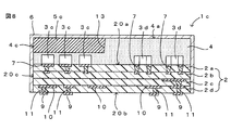
- FIG. 3 is a cross-sectional view of the high-frequency module according to the first embodiment of the present invention, taken along the line AA in FIG.
- FIG. 2 is a plan view of a state in which a top surface of a shield film of the high frequency module of FIG. 1 is removed. It is a perspective view of the components mounted in a wiring board. It is a figure which shows the groove
- FIG. 8 is a cross-sectional view of the high-frequency module according to the second embodiment of the present invention, which is a cross-sectional view taken along the line BB in FIG. 7.
- FIG. 8 is a cross-sectional view of the high-frequency module according to the second embodiment of the present invention, which is a cross-sectional view taken along the line BB in FIG. 7.
- FIG. 7 is a plan view of a state in which a top surface of a shield film of the high frequency module of FIG. 6 is removed.
- FIG. 10 is a cross-sectional view of the high-frequency module according to the third embodiment of the present invention, which is a cross-sectional view taken along the line CC in FIG. 9. It is a top view in the state where the upper surface of the shielding film of the high frequency module of FIG. 8 was removed. It is sectional drawing of the conventional high frequency module.
- FIGS. 1 is a cross-sectional view of the high-frequency module 1a
- FIG. 2 is a plan view of the high-frequency module 1a with the top surface of the shield film 6 removed
- FIG. 3 is a perspective view of a component 3c mounted on the multilayer wiring board 2.
- 4 is a view showing a groove in which the shield wall 5a of FIG. 1 is disposed.
- the high-frequency module 1 a includes a multilayer wiring board 2 (corresponding to “wiring board” of the present invention) and a plurality of components mounted on the upper surface 20 a of the multilayer wiring board 2.
- a multilayer wiring board 2 corresponding to “wiring board” of the present invention
- the sealing resin layer 4 laminated on the upper surface 20a of the multilayer wiring board 2 the shield film 6 covering the surface of the sealing resin layer 4, and the sealing resin layer 4
- it is mounted on a mother board or the like of an electronic device that uses a high-frequency signal.
- the multilayer wiring board 2 is formed by laminating a plurality of insulating layers 2a to 2d made of, for example, a low-temperature co-fired ceramic or glass epoxy resin.
- a mounting electrode 7 for mounting the components 3a and 3b and a surface layer electrode 8a connected to the shield wall 5a are formed on the upper surface 20a of the multilayer wiring board 2 (corresponding to the “main surface of the wiring board” of the present invention).
- a mounting electrode 7 for mounting the components 3a and 3b and a surface layer electrode 8a connected to the shield wall 5a are formed on the lower surface 20b.
- a plurality of external electrodes 9 for external connection are formed on the lower surface 20b.
- various internal wiring electrodes 10 are arranged between the adjacent insulating layers 2a to 2d.
- a plurality of via conductors 11 for connecting the internal wiring electrodes 10 formed in different insulating layers 2a to 2d are formed in the multilayer wiring board 2.
- the surface layer electrode 8a is connected to the internal wiring electrode 10
- the mounting electrode 7, the surface layer electrode 8a, the external electrode 9, and the internal wiring electrode 10 are all made of a metal generally adopted as a wiring electrode such as Cu, Ag, or Al.
- Each via conductor 11 is formed of a metal such as Ag or Cu.
- Each mounting electrode 7, the surface layer electrode 8a, and each external electrode 9 may be subjected to Ni / Au plating.
- Each component 3a to 3d includes a semiconductor element formed of a semiconductor such as Si or GaAs, or a chip component such as a chip inductor, a chip capacitor, or a chip resistor.
- the component 3a (corresponding to one of the “first component” and the “second component” of the present invention) and the component 3b (the “first component” and the “second component” of the present invention) Each) is an active element such as an IC, and the other components 3c and 3d are passive elements such as a chip capacitor and a chip inductor.
- the component 3c constituting the passive element is a general rectangular parallelepiped chip component, and terminal electrodes 12 for external connection are formed at two locations.
- the terminal electrode 12 is disposed at both ends in the longitudinal direction of the rectangular parallelepiped, and one terminal electrode 12 is formed on the entire side surface 3c3 (side surface 3c3 in contact with one short side of the upper surface 3c1) and the side surface 3c3. A part of each of the upper surface 3c1, the lower surface 3c2, and the two side surfaces 3c4 and 3c6 is covered.
- the other terminal electrode 12 covers the entire side surface 3c5 and a part of each of the upper surface 3c1, the lower surface 3c2, and the two side surfaces 3c4 and 3c6 in contact with the side surface 3c5 when facing the one side surface 3c3.
- One terminal electrode 12 is connected to a ground electrode (internal wiring electrode 10) inside multilayer wiring board 2 through mounting electrode 7 and via conductor 11 and the like.
- the lower surface 3c2 of the component 3c facing the upper surface 20a of the multilayer wiring board 2 in the mounted state corresponds to the “first surface of the third component” of the present invention
- the upper surface 3c1 facing the lower surface 3c2 is the main surface.
- Each of the four side surfaces 3c3 to 3c6 connecting the edges of the upper surface 3c1 and the lower surface 3c2 of the component 3c corresponds to the “side surface of the third component” of the present invention. .
- the sealing resin layer 4 is laminated on the multilayer wiring board 2 so as to cover the upper surface 20a of the multilayer wiring board 2 and the components 3a to 3d.
- the sealing resin layer 4 can be formed of a resin that is generally employed as a sealing resin such as an epoxy resin.
- the shield film 6 is for shielding noise from the outside with respect to the various internal wiring electrodes 10 and the components 3a to 3d in the multilayer wiring board 2, and includes the upper surface 4a and the side surface 4c of the sealing resin layer 4, and the multilayer The side surface 20c of the wiring board 2 is covered.
- the shield film 6 may be formed in a multilayer structure having an adhesion film laminated on the surface of the sealing resin layer 4, a conductive film laminated on the adhesion film, and a protective film laminated on the conductive film. it can.
- the adhesion film is provided to increase the adhesion strength between the conductive film and the sealing resin layer 4 and can be formed of a metal such as SUS, for example.
- the conductive film is a layer that bears the substantial shielding function of the shield film 6 and can be formed of, for example, any one of Cu, Ag, and Al.
- the protective film is provided to prevent the conductive film from being corroded or scratched, and can be formed of, for example, SUS.
- the shield wall 5a is formed so as to be disposed at least between the component 3a and the component 3b which are active elements in the sealing resin layer 4. Specifically, as shown in FIG. 2, when viewed from a direction perpendicular to the upper surface 20a of the multilayer wiring board 2, a groove 13 is formed so as to divide the sealing resin layer 4 into two regions.
- the shield wall 5a is formed by filling the groove 13 with a conductive paste mainly composed of Cu, Ag, or the like.
- some of the components 3c are mounted at a position overlapping the shield wall 5a.
- the groove 13 is formed by laser processing.
- the groove 13 in the region overlapping with the component 3c (actually the region adjacent to these components in addition to the region overlapping with the two components 3c) is formed with a depth that does not reach the component 3c, and other regions The groove 13 is formed with a depth at which the surface layer electrode 8a is exposed.
- the groove 13 in the region that does not overlap the part 3c is formed with a step portion 13c (corresponding to the “boundary portion” of the present invention) due to the change in the groove width in the middle of the depth direction (FIG. 4A). )reference).
- the widest groove width W2 of the second step portion 13b (corresponding to the “wide portion” of the present invention) with the shallower depth is the first step portion with the deeper depth.
- This portion 13a (corresponding to the “narrow portion” of the present invention) is formed wider than the widest groove width W1.
- the groove width of the end portion closer to the step portion 13c in the depth direction of the first step portion 13a is equal to that of the second step portion 13b. It is formed smaller than the groove width of the end portion closer to the stepped portion 13c in the depth direction (the minimum groove width W3 of the second step portion 13b).
- the first-stage portion 13a and the second-stage portion 13b of the groove 13 are both formed in an expanded shape in which the groove width increases as the distance from the multilayer wiring board 2 increases in the depth direction.
- the groove 13 in the region overlapping the component 3c has no step and is formed in an expanded shape in which the groove width increases as the distance from the multilayer wiring board 2 increases in the depth direction (see FIG. 4B).
- the widest groove width W4 in this region is formed narrower than the widest groove width W2 in the region that does not overlap the part 3c.
- the shield wall 5a is not formed between the groove 13 and the upper surface 20a of the wiring board 2 in this region.
- the terminal electrode 12 of the component 3c is arranged so as to fill a portion where the shield wall 5a is not formed. Since the terminal electrode 12 is connected to the ground, it is possible to suppress a deterioration in the characteristics of the inter-component shield due to the shield wall 5a.
- the distance L (see FIG. 1) between the bottom of the groove 13 in the region overlapping the part 3c and the upper surface 3c1 of the part 3c is preferably short.
- the distance L should be at least 10 ⁇ m, preferably about 20 ⁇ m.
- the distance L is preferably 1 ⁇ 4 ⁇ or less, where ⁇ is the frequency of the high-frequency signal to be used. Therefore, the component 3c is required to have electrodes on the side surfaces 3c3 to 3c6. However, even when the electrode is on the lower surface 3c2, the distance between the bottom of the groove 13 and the lower surface 3c2 of the component is 1 / 4 ⁇ . This structure will be applied.
- the maximum value of the groove width is required to be at least about 100 ⁇ m in order to ensure the required filling property.
- the groove width W4 may be about 50 ⁇ m.
- the shield wall 5a can be formed not by a conductive paste but also by a plating process. In this case, the conductor can be filled even if the groove width is about 20 ⁇ m.
- the groove 13 in which the shield wall 5a functioning as a shield between parts is disposed is formed at a depth that does not reach the part 3c in the region overlapping with the part 3c. 5a does not restrict the mounting area of the multilayer wiring board 2, and high-density mounting of the components 3a to 3d becomes possible.
- the shield wall 5a is not formed between the bottom of the groove 13 and the upper surface 20a of the wiring board 2 in the region that does not overlap the part 3c of the groove 13, but the part 3c is formed on the side surfaces 3c3 to 3c6.
- the terminal electrode 12 connected to the grant Since the terminal electrode 12 connected to the grant is formed, the terminal electrode 12 can function as a part of the shield between components by closing the hole, and the shield characteristics of the shield wall 5a can be maintained. In addition, by forming a portion that does not reach the upper surface 20a of the multilayer wiring board 2 in a part of the groove 13 that forms the shield wall 5a (a region that overlaps the component 3c), the groove 13 completely covers the sealing resin layer 4. Since the structure is not divided, warping and deformation of the high-frequency module 1a can be suppressed. In this embodiment, the shape of the groove 13 in the region that does not overlap the part 3c is shown as a two-stage shape.
- the present invention is not limited to this, and the depth can be reduced by simply changing the groove width (without a step).
- a changing structure may be used. That is, it may be a groove shape in which the second stage portion 13b and the first stage portion 13a are connected by a gentle curved surface.
- the groove 13 in the region overlapping with the component 3c has a stepless structure, but it may also be a two-step structure with a narrow groove width. For example, when it is desired to reduce the groove width, the groove width can be reduced and the groove depth can be reduced by increasing the laser scanning speed.
- the shield wall 5a is formed of a conductive paste
- the depth of the groove 13 is In the deep region (the region that does not overlap with the component 3c), as shown in FIG. 4A, the formation of the conductive paste into the groove 13 is improved because it is formed in two stages.
- the shield wall 5a overlaps the component 3c in the absence of the terminal electrode 12 when viewed from the direction perpendicular to the upper surface 20a of the multilayer wiring board 2.
- the shield wall 5a may overlap the part 3c where there is the terminal electrode 12 (the portion covering the upper surface 3c1). Since the terminal electrode 12 has a function of reflecting the laser beam and reducing damage to the component 3c, the distance L between the component 3c and the bottom of the groove 13 can be further shortened in this way.
- the distance L is required to be about 10 ⁇ m, preferably about 20 ⁇ m. However, according to this configuration, the distance L can be set to about 5 ⁇ m.
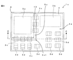
- FIGS. 1 is a cross-sectional view of the high-frequency module 1b
- FIG. 2 is a plan view of the high-frequency module 1b with the upper surface of the shield film 6 removed, corresponding to FIG.
- the high-frequency module 1b according to this embodiment differs from the high-frequency module 1a according to the first embodiment described with reference to FIGS. 1 to 4 in that, as shown in FIG. 6 and FIG.
- the arrangement configuration of the parts is different from the configuration of the surface electrode. Since other configurations are the same as those of the high-frequency module 1a of the first embodiment, description thereof is omitted by attaching the same reference numerals.
- the shield wall 5b is formed in a polygonal line having a bent portion 5b1 when viewed from a direction perpendicular to the upper surface 20a of the multilayer wiring board 2, and the shield wall 5b and the shield film 6 are components.
- Some passive elements (component 3c) are arranged along a line formed by the shield wall 5b when viewed from a direction perpendicular to the upper surface 20a of the multilayer wiring board 2.
- none of the components 3a to 3d are arranged in the region overlapping the bent portion 5b1, and the rectangular surface layer electrode 8b is formed.
- the groove 13 of the bent portion 5b1 where the components 3a to 3d are not disposed is formed at a depth at which the surface layer electrode 8b is exposed, and the shield wall 5b is connected to the surface layer electrode 8b at the bent portion 5b1. Further, the groove 13 in the region other than the bent portion 5b1 is formed with a certain depth that does not reach the component 3c.
- the surface layer electrode 8b is connected to a ground electrode (internal wiring electrode 10) formed inside the multilayer wiring board 2.
- the groove 13 of the shield wall 5b is formed by laser processing or the like, if there is a bent portion 5b1 in the groove 13, the energy of the laser beam acts on this part more strongly than the other part. Deepen. Therefore, according to this configuration, since the components 3a to 3d are not arranged in the bent portion 5b1, it is possible to suppress the influence of the laser beam on the characteristics of the components 3a to 3d when the groove 13 is formed. Moreover, since it is not necessary to change the irradiation condition of the laser beam according to the location of the groove 13, the shield wall 5b can be easily formed.
- the groove 13 of the shield wall 5b is formed with a depth at which the surface layer electrode 8b is exposed only in a region near the bent portion 5b1, and the other region is formed with a depth that does not reach the upper surface 20a of the multilayer wiring board 2.
- the components 3a to 3 can be mounted at high density. In this case, there is a possibility that the hole of the shield wall 5b becomes wide and the shield characteristics deteriorate.
- the terminal electrode 12 of each component 3c can function as a part of the shield between components. It is possible to suppress the deterioration of the shield characteristics due to.
- FIGS. 8 is a cross-sectional view of the high-frequency module 1c
- FIG. 9 is a plan view of the high-frequency module 1c with the top surface of the shield film 6 removed, corresponding to FIG.
- the high-frequency module 1c according to this embodiment differs from the high-frequency module 1b according to the second embodiment described with reference to FIGS. 6 and 7 in that a surface layer electrode is provided as shown in FIGS. There is no difference and the configuration of the shield wall is different. Since other configurations are the same as those of the high-frequency module 1b of the second embodiment, description thereof is omitted by attaching the same reference numerals.
- the shield wall 5b of the second embodiment described above is formed with a depth that allows the groove 13 of the bent portion 5b1 to reach the upper surface 20a of the multilayer wiring board 2.
- the shield wall 5c of this embodiment has the bent portion 5c1.
- the groove 13 is formed with the same depth as the groove 13 in the region other than the bent portion 5c1. That is, the shield wall 5c does not have a portion that contacts the upper surface 20a of the multilayer wiring board 2, and the groove 13 of the shield wall 5c is formed at a certain depth that does not reach the component 3c in the entire region.
- the shield film 6 is connected to the ground electrode (internal wiring electrode 10) exposed on the side surface 20c of the multilayer wiring board 2.
- the shield wall 5 c is grounded through the shield film 6 because the upper end portion is connected to the shield film 6.
- the groove 13 in which the shield wall 5c is disposed does not reach the upper surface 20a of the multilayer wiring board 2, when the groove 13 is formed by laser processing, the groove 13 is formed on the multilayer wiring board 2 by laser light. The influence can be suppressed.
- the component mounting area increases, the components can be mounted at high density.
- the groove can be formed under one laser light irradiation condition, so that the shield wall 5c can be easily formed.
- the groove 13 forming the shield wall 5c is formed at a depth that does not reach the upper surface 20a of the multilayer wiring board 2 in the entire region, so that the groove 13 does not completely divide the sealing resin layer 4. Therefore, warpage and deformation of the high frequency module 1c can be suppressed.
- the groove 13 in which the shield wall 5a of the first embodiment described above is disposed has the widest groove width W4 in the region overlapping with the component 3c, which is the largest of the second-stage portion 13b in the region not overlapping with the component 3c.
- the groove widths may be the same or similar.
- the number of insulating layers and wiring layers constituting the multilayer wiring board 2 can be changed as appropriate.
- the present invention can be applied to various high-frequency modules including a sealing resin layer that covers components mounted on a wiring board and a shield wall that prevents mutual interference of noise between components.
Abstract
Le but de la présente invention est de permettre un montage à haute densité de composants dans une configuration pourvue d'un blindage de composant à composant, et de maintenir une caractéristique de protection de composant à composant. Un module haute fréquence 1a est pourvu : d'une carte de câblage multicouche 2 ; d'une pluralité de composants 3a à 3d montés sur une surface supérieure 20a de la carte de câblage multicouche 2 ; d'une couche de résine d'étanchéité 4 qui est empilée sur la surface supérieure 20a de la carte de câblage multicouche 2 et qui scelle la pluralité de composants 3a à 3d ; et d'une paroi de blindage 5a qui est disposée dans une rainure 13 formée entre un composant 3a et un composant 3b de la couche de résine d'étanchéité 4. La paroi de blindage 5a, vue depuis une direction perpendiculaire à la surface supérieure 20a de la carte de câblage multicouche 2, comprend une région chevauchant le composant 3c. La rainure 13 dans la région de chevauchement est formée avec une profondeur qui n'atteint pas le composant 3c. Le composant 3c présente des surfaces latérales 3c3, 3c5 qui sont entièrement recouvertes d'une électrode de borne 12, et une surface supérieure 3c1, une surface inférieure 3c2, et des surfaces latérales 3c4, 3c6 qui sont partiellement recouvertes de celle-ci.
Priority Applications (2)
| Application Number | Priority Date | Filing Date | Title |
|---|---|---|---|
| CN201880020282.8A CN110506457B (zh) | 2017-03-31 | 2018-03-29 | 高频模块 |
| US16/581,887 US11291108B2 (en) | 2017-03-31 | 2019-09-25 | Radio-frequency module with shield wall |
Applications Claiming Priority (2)
| Application Number | Priority Date | Filing Date | Title |
|---|---|---|---|
| JP2017072318 | 2017-03-31 | ||
| JP2017-072318 | 2017-03-31 |
Related Child Applications (1)
| Application Number | Title | Priority Date | Filing Date |
|---|---|---|---|
| US16/581,887 Continuation US11291108B2 (en) | 2017-03-31 | 2019-09-25 | Radio-frequency module with shield wall |
Publications (1)
| Publication Number | Publication Date |
|---|---|
| WO2018181709A1 true WO2018181709A1 (fr) | 2018-10-04 |
Family
ID=63678008
Family Applications (1)
| Application Number | Title | Priority Date | Filing Date |
|---|---|---|---|
| PCT/JP2018/013235 WO2018181709A1 (fr) | 2017-03-31 | 2018-03-29 | Module haute fréquence |
Country Status (3)
| Country | Link |
|---|---|
| US (1) | US11291108B2 (fr) |
| CN (1) | CN110506457B (fr) |
| WO (1) | WO2018181709A1 (fr) |
Cited By (1)
| Publication number | Priority date | Publication date | Assignee | Title |
|---|---|---|---|---|
| WO2021131776A1 (fr) * | 2019-12-27 | 2021-07-01 | 株式会社村田製作所 | Module |
Families Citing this family (2)
| Publication number | Priority date | Publication date | Assignee | Title |
|---|---|---|---|---|
| US20220066036A1 (en) * | 2020-08-25 | 2022-03-03 | Lumentum Operations Llc | Package for a time of flight device |
| US20230092873A1 (en) * | 2021-09-23 | 2023-03-23 | Advanced Semiconductor Engineering, Inc. | Semiconductor device package |
Citations (3)
| Publication number | Priority date | Publication date | Assignee | Title |
|---|---|---|---|---|
| JPH06252581A (ja) * | 1993-02-24 | 1994-09-09 | Murata Mfg Co Ltd | 貫通コンデンサの取付け構造 |
| JP2015057804A (ja) * | 2013-08-13 | 2015-03-26 | 太陽誘電株式会社 | 回路モジュール |
| JP2015111747A (ja) * | 2013-10-30 | 2015-06-18 | 太陽誘電株式会社 | 通信モジュール |
Family Cites Families (9)
| Publication number | Priority date | Publication date | Assignee | Title |
|---|---|---|---|---|
| WO2006059556A1 (fr) | 2004-12-02 | 2006-06-08 | Murata Manufacturing Co., Ltd. | Composant electronique et son procede de production |
| CN101978490B (zh) * | 2008-03-31 | 2012-10-17 | 株式会社村田制作所 | 电子元器件组件及该电子元器件组件的制造方法 |
| JP6113585B2 (ja) * | 2013-06-26 | 2017-04-12 | 富士通コンポーネント株式会社 | 電子部品モジュール、基板及び電子部品モジュールの製造方法 |
| JP5622906B1 (ja) | 2013-08-09 | 2014-11-12 | 太陽誘電株式会社 | 回路モジュールの製造方法 |
| CN104602366B (zh) * | 2013-10-30 | 2018-09-25 | 太阳诱电株式会社 | 通信模块 |
| US9160825B2 (en) | 2013-10-30 | 2015-10-13 | Taiyo Yuden Co., Ltd. | Communication module |
| JP5958454B2 (ja) * | 2013-12-05 | 2016-08-02 | 株式会社村田製作所 | 部品内蔵モジュール |
| WO2017043621A1 (fr) * | 2015-09-11 | 2017-03-16 | 株式会社村田製作所 | Module haute fréquence |
| US20180090466A1 (en) * | 2016-09-29 | 2018-03-29 | Advanced Semiconductor Engineering, Inc. | Semiconductor device package and method of manufacturing the same |
-
2018
- 2018-03-29 CN CN201880020282.8A patent/CN110506457B/zh active Active
- 2018-03-29 WO PCT/JP2018/013235 patent/WO2018181709A1/fr active Application Filing
-
2019
- 2019-09-25 US US16/581,887 patent/US11291108B2/en active Active
Patent Citations (3)
| Publication number | Priority date | Publication date | Assignee | Title |
|---|---|---|---|---|
| JPH06252581A (ja) * | 1993-02-24 | 1994-09-09 | Murata Mfg Co Ltd | 貫通コンデンサの取付け構造 |
| JP2015057804A (ja) * | 2013-08-13 | 2015-03-26 | 太陽誘電株式会社 | 回路モジュール |
| JP2015111747A (ja) * | 2013-10-30 | 2015-06-18 | 太陽誘電株式会社 | 通信モジュール |
Cited By (1)
| Publication number | Priority date | Publication date | Assignee | Title |
|---|---|---|---|---|
| WO2021131776A1 (fr) * | 2019-12-27 | 2021-07-01 | 株式会社村田製作所 | Module |
Also Published As
| Publication number | Publication date |
|---|---|
| US11291108B2 (en) | 2022-03-29 |
| US20200022250A1 (en) | 2020-01-16 |
| CN110506457B (zh) | 2021-03-12 |
| CN110506457A (zh) | 2019-11-26 |
Similar Documents
| Publication | Publication Date | Title |
|---|---|---|
| JP7120295B2 (ja) | 高周波モジュール | |
| US10849257B2 (en) | Module | |
| JP6806166B2 (ja) | 高周波モジュール | |
| US10349512B2 (en) | High-frequency module | |
| US10312172B2 (en) | High-frequency module | |
| JP6965928B2 (ja) | 高周波モジュール | |
| WO2018164158A1 (fr) | Module à haute fréquence | |
| US10667381B2 (en) | High frequency module | |
| US5235208A (en) | Package for microwave integrated circuit | |
| JP7111112B2 (ja) | 高周波モジュール | |
| JP7067609B2 (ja) | 高周波モジュール | |
| WO2017043621A1 (fr) | Module haute fréquence | |
| WO2018181709A1 (fr) | Module haute fréquence | |
| US11348894B2 (en) | High-frequency module | |
| JP6900660B2 (ja) | シールド層を有するモジュール | |
| US10546820B2 (en) | Radio frequency module and method for manufacturing the same | |
| US20230199965A1 (en) | Circuit module and method for manufacturing submodule | |
| US20220159825A1 (en) | Module |
Legal Events
| Date | Code | Title | Description |
|---|---|---|---|
| 121 | Ep: the epo has been informed by wipo that ep was designated in this application |
Ref document number: 18774342 Country of ref document: EP Kind code of ref document: A1 |
|
| NENP | Non-entry into the national phase |
Ref country code: DE |
|
| 122 | Ep: pct application non-entry in european phase |
Ref document number: 18774342 Country of ref document: EP Kind code of ref document: A1 |
|
| NENP | Non-entry into the national phase |
Ref country code: JP |