WO2018180522A1 - 固体撮像装置、電子機器、及び駆動方法 - Google Patents
固体撮像装置、電子機器、及び駆動方法 Download PDFInfo
- Publication number
- WO2018180522A1 WO2018180522A1 PCT/JP2018/010124 JP2018010124W WO2018180522A1 WO 2018180522 A1 WO2018180522 A1 WO 2018180522A1 JP 2018010124 W JP2018010124 W JP 2018010124W WO 2018180522 A1 WO2018180522 A1 WO 2018180522A1
- Authority
- WO
- WIPO (PCT)
- Prior art keywords
- transistor
- signal
- pixel
- selection
- reset
- Prior art date
- Legal status (The legal status is an assumption and is not a legal conclusion. Google has not performed a legal analysis and makes no representation as to the accuracy of the status listed.)
- Ceased
Links
Images









Classifications
-
- H—ELECTRICITY
- H04—ELECTRIC COMMUNICATION TECHNIQUE
- H04N—PICTORIAL COMMUNICATION, e.g. TELEVISION
- H04N25/00—Circuitry of solid-state image sensors [SSIS]; Control thereof
- H04N25/70—SSIS architectures; Circuits associated therewith
- H04N25/76—Addressed sensors, e.g. MOS or CMOS sensors
- H04N25/77—Pixel circuitry, e.g. memories, A/D converters, pixel amplifiers, shared circuits or shared components
-
- H—ELECTRICITY
- H04—ELECTRIC COMMUNICATION TECHNIQUE
- H04N—PICTORIAL COMMUNICATION, e.g. TELEVISION
- H04N25/00—Circuitry of solid-state image sensors [SSIS]; Control thereof
- H04N25/50—Control of the SSIS exposure
- H04N25/57—Control of the dynamic range
- H04N25/571—Control of the dynamic range involving a non-linear response
- H04N25/573—Control of the dynamic range involving a non-linear response the logarithmic type
-
- H—ELECTRICITY
- H04—ELECTRIC COMMUNICATION TECHNIQUE
- H04N—PICTORIAL COMMUNICATION, e.g. TELEVISION
- H04N25/00—Circuitry of solid-state image sensors [SSIS]; Control thereof
- H04N25/70—SSIS architectures; Circuits associated therewith
- H04N25/76—Addressed sensors, e.g. MOS or CMOS sensors
- H04N25/766—Addressed sensors, e.g. MOS or CMOS sensors comprising control or output lines used for a plurality of functions, e.g. for pixel output, driving, reset or power
-
- H—ELECTRICITY
- H04—ELECTRIC COMMUNICATION TECHNIQUE
- H04N—PICTORIAL COMMUNICATION, e.g. TELEVISION
- H04N25/00—Circuitry of solid-state image sensors [SSIS]; Control thereof
- H04N25/70—SSIS architectures; Circuits associated therewith
- H04N25/76—Addressed sensors, e.g. MOS or CMOS sensors
- H04N25/77—Pixel circuitry, e.g. memories, A/D converters, pixel amplifiers, shared circuits or shared components
- H04N25/778—Pixel circuitry, e.g. memories, A/D converters, pixel amplifiers, shared circuits or shared components comprising amplifiers shared between a plurality of pixels, i.e. at least one part of the amplifier must be on the sensor array itself
-
- H—ELECTRICITY
- H10—SEMICONDUCTOR DEVICES; ELECTRIC SOLID-STATE DEVICES NOT OTHERWISE PROVIDED FOR
- H10F—INORGANIC SEMICONDUCTOR DEVICES SENSITIVE TO INFRARED RADIATION, LIGHT, ELECTROMAGNETIC RADIATION OF SHORTER WAVELENGTH OR CORPUSCULAR RADIATION
- H10F39/00—Integrated devices, or assemblies of multiple devices, comprising at least one element covered by group H10F30/00, e.g. radiation detectors comprising photodiode arrays
- H10F39/10—Integrated devices
- H10F39/12—Image sensors
Definitions
- the present disclosure relates to a solid-state imaging device, an electronic device, and a driving method, and more particularly, to a solid-state imaging device, an electronic device, and a driving method that can realize multi-pixels while suppressing power consumption of pixels. .
- a logarithmic sensor (Logarithmic Image Sensor) is known that operates an open circuit in the same manner as a solar cell to measure an output voltage (see, for example, Non-Patent Document 1).
- Such a logarithmic sensor in the solar cell mode uses a potential difference generated when a current flows in the forward direction of the PN junction, that is, a relationship in which the voltage is proportional to the logarithm of the current. If this forward current is replaced with a photocurrent generated by photoelectric conversion and the forward voltage of the PN junction is monitored, it becomes a signal obtained by logarithmically compressing the photocurrent.
- the structure of each pixel is a two-stage amplifier composed of two stages.
- an amplifier structure is employed.
- the present disclosure has been made in view of such a situation, and in a logarithmic sensor in a solar cell mode, the power consumption of a pixel can be suppressed and a large number of pixels can be realized.
- a solid-state imaging device includes a photoelectric conversion unit, a reset transistor that resets the photoelectric conversion unit in response to a reset signal, a first amplification transistor that amplifies a signal from the photoelectric conversion unit, In response to a selection signal, a selection transistor that selects a signal from the first amplification transistor, a second amplification transistor that amplifies the signal from the selection transistor and applies the signal to a vertical signal line, the selection transistor, and the selection transistor A pixel connected to a second amplifying transistor and having a bias transistor functioning as a current source, the pixel having a logarithmic characteristic output signal and having a pixel array section arranged in a matrix; The amplification transistor and the second amplification transistor are each a solid-state imaging device connected to a power supply voltage.
- An electronic apparatus includes a photoelectric conversion unit, a reset transistor that resets the photoelectric conversion unit according to a reset signal, a first amplification transistor that amplifies a signal from the photoelectric conversion unit, and a selection A selection transistor that selects a signal from the first amplification transistor according to a signal, a second amplification transistor that amplifies the signal from the selection transistor and applies the signal to a vertical signal line, the selection transistor, and the first transistor A pixel array unit that is connected to two amplification transistors and has a bias transistor that functions as a current source, and in which the pixels from which logarithmic characteristic output signals are obtained are arranged in a matrix, the first amplification An electronic device including a transistor and a solid-state imaging device each connected to a power supply voltage A.
- a photoelectric conversion unit a reset transistor that resets the photoelectric conversion unit according to a reset signal, and a first signal that amplifies a signal from the photoelectric conversion unit
- a pixel array unit is provided that includes a bias transistor that is connected to a selection transistor and the second amplifying transistor and functions as a current source, and in which the pixels from which a logarithmic characteristic output signal is obtained are arranged in a matrix.
- the first amplification transistor and the second amplification transistor are connected to a power supply voltage, respectively. Configured.
- solid-state imaging device or electronic device may be an independent device, or may be an internal block constituting one device.
- a driving method includes: a photoelectric conversion unit; a reset transistor that resets the photoelectric conversion unit in response to a reset signal; a first amplification transistor that amplifies a signal from the photoelectric conversion unit; A selection transistor that selects a signal from the first amplification transistor according to a signal, a second amplification transistor that amplifies the signal from the selection transistor and applies the signal to a vertical signal line, the selection transistor, and the first transistor
- a pixel array unit that is connected to two amplification transistors and has a bias transistor that functions as a current source, and in which the pixels from which logarithmic characteristic output signals are obtained are arranged in a matrix, the first amplification
- the transistor and the second amplification transistor are each a driving method of a solid-state imaging device connected to a power supply voltage.
- the reset transistor is driven to be in an on state during a shutter driving period prior to an exposure period, and the selection transistor is driven to be in an on state during a readout period after the exposure period, so that the reading is performed.
- the reset transistor is driven to be in an on state when a reset level is read during the period.
- the reset transistor is driven to be in an on state in a shutter driving period before the exposure period, and the selection transistor is in an on state in a readout period after the exposure period.
- the reset transistor is driven so as to be in an on state at the time of reading the reset level in the reading period.
- a driving method includes: a photoelectric conversion unit; a reset transistor that resets the photoelectric conversion unit in response to a reset signal; a first amplification transistor that amplifies a signal from the photoelectric conversion unit; A selection transistor that selects a signal from the first amplification transistor according to a signal, a second amplification transistor that amplifies the signal from the selection transistor and applies the signal to a vertical signal line, the selection transistor, and the first transistor
- a pixel array unit that is connected to two amplification transistors and has a bias transistor that functions as a current source, and in which the pixels from which logarithmic characteristic output signals are obtained are arranged in a matrix, the first amplification
- the transistor and the second amplification transistor are each a driving method of a solid-state imaging device connected to a power supply voltage.
- the reset transistor is driven to be in an on state during a shutter driving period prior to an exposure period, and the selection transistor is driven to be in an on state during a readout period after the exposure period, so that the reading is performed.
- the reset transistor is driven to be in an on state at the time of reading a reset level in a period, and the bias transistor is driven to be in an off state except for the reading period.
- the reset transistor is driven to be in an on state in a shutter driving period before the exposure period, and the selection transistor is in an on state in a readout period after the exposure period.
- the reset transistor is driven to be turned on, and the bias transistor is driven to be turned off except in the reading period.
- FIG. 12 is a cross-sectional view illustrating another configuration example of a stacked solid-state imaging device to which the technology according to the present disclosure can be applied.
- It is a block diagram which shows an example of a schematic structure of a vehicle control system. It is explanatory drawing which shows an example of the installation position of a vehicle exterior information detection part and an imaging part. It is a block diagram which shows an example of a schematic structure of an in-vivo information acquisition system.
- FIG. 1 is a diagram illustrating a pixel configuration of a logarithmic sensor in a general solar cell mode.
- the pixel 900 of the general logarithmic sensor shown in FIG. 1 is one of a plurality of pixels arranged in a matrix in a pixel array unit in a solid-state imaging device such as a CMOS (Complementary Metal Oxide Semiconductor) image sensor. This corresponds to one pixel.
- CMOS Complementary Metal Oxide Semiconductor
- a pixel 900 of a general logarithmic sensor includes a photodiode 911, a reset transistor 912, an amplification transistor 913, a bias transistor 914, an amplification transistor 915, and a selection transistor 916.
- the photodiode 911 is a photoelectric conversion unit including n-type and p-type semiconductor regions.
- the reset transistor 912 controls the resetting of the photodiode 911 in accordance with on / off of a reset signal (RST) applied to the gate electrode.
- RST reset signal
- the amplification transistor 913 amplifies the signal from the photodiode 911 applied to the gate electrode and outputs the amplified signal to the amplification transistor 915.
- the bias transistor 914 functions as a current source.
- the amplification transistor 915 amplifies the signal from the photodiode 911 applied to the gate electrode and outputs the amplified signal to the selection transistor 916.
- the selection transistor 916 outputs a signal from the amplification transistor 915 to the vertical signal line 921 in accordance with the on / off of the selection signal (SEL) applied to the gate electrode.
- the amplification transistor as the first stage amplifier (AMP1).
- a two-stage amplifier structure including 913 and an amplification transistor 915 as a second-stage amplifier (AMP2) is employed.
- a bias transistor 914 functioning as a current source in the pixel 900.
- a bias current I Bias flows constantly.
- FIG. 2 is a timing chart for explaining a driving method of the pixel 900 (FIG. 1) of the logarithmic sensor in a general solar cell mode.
- the level of the signal (RST) is represented in time series.
- the level of the signal (VSL) applied to the vertical signal line 921 is represented in time series.
- Pre-Shutter represents the shutter drive period
- Exposure represents the exposure period
- Readout represents the readout period.
- the time direction is a direction from the left side to the right side in the figure, and the periods transition in the order of the shutter driving period, the exposure period, and the readout period.
- the reset signal (RST) becomes H level, and the reset transistor 912 resets the photodiode 911 to a low potential.
- the charge accumulated in the photodiode 911 is read by the selection transistor 916 as a signal level (S: Signal), and then the reset signal (RST) becomes H level, and the photodiode 911 is read.
- the noise level (N: Noise) is read out with the reset.
- the difference (S ⁇ N) between the signal level (S) and the noise level (N) obtained in this way is the output signal (Output).
- the selection signal (SEL) becomes the L level and the selection transistor 916 is turned off
- the output of the amplification transistor 915 is cut off, and the vertical signal line (VSL) 921 reaches the vicinity of the ground (GND).
- the potential will be lowered.
- the bias current I Bias always flows in the bias transistor 914.
- a linear signal (a signal proportional to the intensity of light) is output until the charge is accumulated in the photodiode 911, and the charge is applied to the photodiode 911.
- the current flows exponentially with respect to the generated voltage. Therefore, the voltage and the current have a logarithmic relationship, and the output of the logarithmic signal is started.
- the amplification transistor 913 As a two-stage amplifier structure. That is, in the pixel 900 of a general logarithmic sensor, in order not to superimpose the potential fluctuation of the transient response VSL of the photodiode 911, the amplification transistor 913 as the first stage amplifier (AMP1) and the second stage amplifier (AMP2). ) As a two-stage amplifier structure.
- a bias transistor 914 that functions as a current source needs to be mounted in the pixel 900.
- the bias transistor 914 by mounting the bias transistor 914, the amplification transistor 913 as the first stage amplifier (AMP1) is always in operation, and the bias current I Bias constantly flows in the pixel 900. (Current is always flowing through the bias transistor 914), and power consumption increases. Such an increase in power consumption becomes a parameter that controls the increase in the number of pixels, and as a result, becomes an obstacle to the increase in the number of pixels.
- the logarithmic sensor in the solar cell mode (solid-state imaging) that can realize the increase in the number of pixels by suppressing the power consumption of the pixel. Equipment).
- solid-state imaging device having a configuration for solving such problems will be described.
- FIG. 3 is a diagram illustrating an embodiment of a solid-state imaging device to which the present technology is applied.
- the solid-state imaging device 10 in FIG. 3 is a solid-state imaging device using CMOS (Complementary Metal Metal Oxide Semiconductor).
- CMOS Complementary Metal Metal Oxide Semiconductor
- the solid-state imaging device 10 takes in incident light (image light) from a subject via an optical lens system (not shown), and converts the amount of incident light imaged on the imaging surface into an electrical signal in units of pixels. Output as a pixel signal.
- the solid-state imaging device 10 includes a pixel array unit 11, a vertical drive circuit 12, a column signal processing circuit 13, a horizontal drive circuit 14, an output circuit 15, a control circuit 16, and an input / output terminal 17. .
- the pixel 100 includes a photodiode (PD) as a photoelectric conversion region and a plurality of pixel transistors.
- PD photodiode
- the vertical drive circuit 12 includes, for example, a shift register, selects a predetermined pixel drive line 21, supplies a pulse for driving the pixel 100 to the selected pixel drive line 21, and sets the pixels 100 in units of rows. To drive. That is, the vertical drive circuit 12 selectively scans each pixel 100 of the pixel array unit 11 in the vertical direction sequentially in units of rows, and is based on the signal charge (charge) generated according to the amount of light received by the photodiode of each pixel 100. The pixel signal is supplied to the column signal processing circuit 13 through the vertical signal line 22.
- the column signal processing circuit 13 is arranged for each column of the pixels 100, and performs signal processing such as noise removal on the signal output from the pixels 100 for one row for each pixel column.
- the column signal processing circuit 13 performs signal processing such as CDS (Correlated Double Sampling) and A / D (Analog / Digital) conversion for removing fixed pattern noise unique to a pixel.
- the horizontal drive circuit 14 is constituted by, for example, a shift register, and sequentially outputs horizontal scanning pulses to sequentially select each of the column signal processing circuits 13, and outputs a pixel signal from each of the column signal processing circuits 13 to the horizontal signal line. 23 to output.
- the output circuit 15 performs signal processing on the signals sequentially supplied from each of the column signal processing circuits 13 through the horizontal signal line 23 and outputs the signals.
- the output circuit 15 may perform only buffering, for example, or may perform black level adjustment, column variation correction, various digital signal processing, and the like.
- the control circuit 16 controls the operation of each part of the solid-state imaging device 10.
- the control circuit 16 receives an input clock signal and data for instructing an operation mode, and outputs data such as internal information of the solid-state imaging device 10. That is, the control circuit 16 uses the vertical synchronization signal, the horizontal synchronization signal, and the master clock signal as a reference for the operation of the vertical drive circuit 12, the column signal processing circuit 13, the horizontal drive circuit 14, and the like. Generate a signal.
- the control circuit 16 outputs the generated clock signal and control signal to the vertical drive circuit 12, the column signal processing circuit 13, the horizontal drive circuit 14, and the like.
- the input / output terminal 17 exchanges signals with the outside.
- the solid-state imaging device 10 of FIG. 3 configured as described above has a solar cell mode in which logarithmic characteristic output signals can be obtained from the pixels 100 arranged in a two-dimensional shape (matrix) in the pixel array unit 11. Configured as a logarithmic sensor.
- the configuration of the pixels 100 arranged two-dimensionally in the pixel array unit 11 of the solid-state imaging device 10 the configuration of the pixels in the first to fifth embodiments described later may be employed. it can.
- configuration examples of the pixels according to the first to fifth embodiments arranged in the pixel array unit 11 will be described.
- the pixel of the first embodiment is described as a pixel 100 to distinguish it from the pixels of other embodiments.
- the pixels of the second to fifth embodiments are described as a pixel 200, a pixel 300, a pixel 400, and a pixel 500, respectively, and these pixels are also described as the solid-state imaging device 10 (FIG. 1). There is no change in the two-dimensional arrangement in the pixel array section 11.
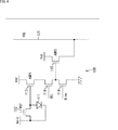
- FIG. 4 is a circuit diagram illustrating a configuration example of the pixel according to the first embodiment.
- the pixel 100 includes a photodiode 111, a reset transistor 112, an amplification transistor 113, a bias transistor 114, an amplification transistor 115, and a selection transistor 116.
- the photodiode 111 is a photoelectric conversion unit including n-type and p-type semiconductor regions.
- the cathode electrode is connected to the intermediate potential Vmid and the drain of the reset transistor 112
- the anode electrode is connected to the source of the reset transistor 112 and the gate of the amplification transistor 113.
- the drain is connected to the intermediate potential Vmid and the cathode electrode of the photodiode 111, and the source is connected to the anode electrode of the photodiode 111 and the gate of the amplification transistor 113.
- a reset signal (RST) is applied to the gate electrode of the reset transistor 112. When this reset signal (RST) becomes active, the reset gate of the reset transistor 112 becomes conductive, and the potential of the photodiode 111 is reset.
- the amplification transistor 113 In the amplification transistor 113, its drain is connected to the power supply voltage Vdd, and its source is connected to the drain of the selection transistor 116.
- the gate of the amplification transistor 113 is connected to the photodiode 111 and the source of the reset transistor 112. Since the signal from the photodiode 111 is applied to the gate of the amplification transistor 113, the signal is amplified and output to the selection transistor 116.
- the drain is connected to the source of the amplification transistor 113, and the source is connected to the drain of the bias transistor 114 and the gate of the amplification transistor 115.
- a selection signal (SEL) is applied to the gate electrode of the selection transistor 116.
- the selection transistor 116 is in a conductive state, and the pixel 100 is in a selection state.
- a signal output from the amplification transistor 113 is output to the amplification transistor 115 via the selection transistor 116.
- the drain is connected to the source of the selection transistor 116 and the gate of the amplification transistor 115, and the source is grounded.
- a predetermined signal is applied to the gate electrode of the bias transistor 114 to set a reference current.
- the bias transistor 114 functions as a current source.
- the amplifying transistor 115 has a drain connected to the power supply voltage Vdd and a source connected to the vertical signal line (VSL) 121 (vertical signal line 22 in FIG. 3).
- the gate of the amplification transistor 115 is connected to the source of the selection transistor 116 and the drain of the bias transistor 114.
- the selection signal (SEL) becomes conductive in the selection transistor 116
- a signal output from the amplification transistor 113 is applied to the gate of the amplification transistor 115 via the selection transistor 116.
- the amplification transistor 115 amplifies the signal applied to its gate and outputs it to the vertical signal line 121.
- the amplification transistor 113 provided on the photodiode 111 side of the amplification transistor 113 and the amplification transistor 115 corresponds to the first stage amplifier (AMP1) and is provided on the vertical signal line (VSL) 121 side.
- the amplifying transistor 115 corresponds to a second-stage amplifier (AMP2).
- the first-stage amplifier (AMP1) and the second-stage amplifier (AMP2) constitute a two-stage amplifier.
- the selection transistor 116 Compared to a general logarithmic sensor pixel 900 (FIG. 1), the selection transistor 116 has two stages. The difference is that the eye amp (AMP2) is moved to the first amp (AMP1).
- the photodiode 111 and the amplification transistor are compared.
- the polarity of the bias transistor 114, the amplification transistor 115, and the selection transistor 116 are inverted.
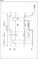
- FIG. 5 is a timing chart illustrating a pixel driving method according to the first embodiment.
- the level of the bias signal (Bias) applied to the gate electrode of the bias transistor 114 are represented in time series.
- the levels of the signal (AMP1_S) applied to the source of the amplification transistor 113 and the signal (VSL) applied to the vertical signal line 121 are represented in time series.
- Pre-Shutter represents the shutter drive period
- Exposure represents the exposure period
- Readout represents the readout period.
- the time direction is a direction from the left side to the right side in the figure, and the periods transition in the order of the shutter driving period, the exposure period, and the readout period.
- the reset signal (RST) becomes H level, and the reset transistor 112 resets the photodiode 111 to a low potential.
- the exposure period is entered.
- the photodiode 111 During the exposure period, charges are accumulated in the photodiode 111. In this exposure period, the signal from the photodiode 111 is applied to the gate of the amplification transistor 113 as the first stage amplifier (AMP1), and the signal is amplified. As shown by the dotted line in the figure, the amplification transistor The potential of the source 113 (AMP1_S) fluctuates.
- the bias transistor 114 starts from the power supply voltage Vdd connected to the drain of the amplification transistor 113. Disconnected.
- the through current (bias current) generated in the pixel 900 (FIG. 1) of a general logarithmic sensor is cut off, the pixel 100 (FIG. 4) is compared with the pixel 900 (FIG. 1). As a result, power consumption is suppressed.
- the selection signal (SEL) becomes H level, and the charge accumulated in the photodiode 111 is read out by the selection transistor 116.
- the charge accumulated in the photodiode 111 is read as the signal level (S: Signal) by the selection transistor 116.
- the noise level (N: Noise) is read out by the selection transistor 116 in a state where the reset signal (RST) becomes H level and the photodiode 111 is reset. It is.
- the difference (SN) between the signal level (S) and the noise level (N) obtained in this way becomes an output signal (Output), and through the amplification transistor 115 as the second-stage amplifier (AMP2), It is output to the vertical signal line 121.
- the selection transistor 116 is turned on (the selection signal (SEL) is at the H level), and the second-stage amplifier is output by the output of the amplification transistor 113 as the first-stage amplifier (AMP1) at the time of D-phase reading.
- the amplification transistor 115 as (AMP2) is naturally activated.
- the selection transistor 116 when the selection transistor 116 is turned off (the selection signal (SEL) is at L level), the bias transistor 114 lowers its drain to near the ground (GND).
- the amplification transistor 115 as the second-stage amplifier (AMP2) is naturally inactivated. Thereby, in the pixel 100 (FIG. 4), the two-stage amplifier including the first-stage amplifier (AMP1) and the second-stage amplifier (AMP2) is automatically turned off.
- a linear signal (a signal proportional to the light intensity) is output until the charge is accumulated in the photodiode 111, and the charge is applied to the photodiode 111.
- the current flows exponentially with respect to the generated voltage. Therefore, the voltage and the current have a logarithmic relationship, and the output of the logarithmic signal is started.
- the selection transistor 116 is turned off because the selection transistor 116 is provided not on the second-stage amplifier (AMP2) side but on the first-stage amplifier (AMP1) side.
- the bias transistor 114 is disconnected from the power supply voltage Vdd connected to the drain of the amplification transistor 113.
- the through current (bias current) generated in the pixel 900 (FIG. 1) of a general logarithmic sensor can be cut off.
- the first embodiment has been described above.
- FIG. 6 is a circuit diagram illustrating a configuration example of a pixel according to the second embodiment.
- the pixel 200 includes a photodiode 211, a reset transistor 212, an amplification transistor 213, a bias transistor 214, an amplification transistor 215, and a selection transistor 216.
- the photodiode 211 to the selection transistor 216 are configured similarly to the photodiode 111 to the selection transistor 116 in the pixel 100 in FIG. 4, but the bias transistor 214 is driven by the bias transistor 114 in FIG. 4. The drive is different.
- the bias signal (Bias) applied to the gate electrode of the bias transistor 214 is controlled, and is driven so that the bias transistor 214 is turned off except for the reading period. This is different from the pixel 100 of FIG.
- FIG. 7 is a timing chart illustrating a pixel driving method according to the second embodiment.
- the timing chart of FIG. 7 shows the selection signal (SEL) of the selection transistor 216, the reset signal (RST) of the reset transistor 212, and the bias signal (Bias) of the bias transistor 214 in the pixel 200 (FIG. 6) of the logarithmic sensor. Levels are represented in time series. In the timing chart of FIG. 7, the level of the signal (AMP1_S) applied to the source of the amplification transistor 213 and the signal (VSL) applied to the vertical signal line 221 is represented in time series.
- the time direction is the direction from the left side to the right side in the drawing, and the shutter drive period (Pre Shutter), exposure period (Exposure), and readout period (The period transitions in the order of “Readout”.
- the reset signal (RST) becomes H level, and the reset transistor 212 resets the photodiode 211 to a low potential.
- the bias signal (Bias) in the shutter driving period and the exposure period is at the L level and the bias transistor 214 is turned off, no bias current flows through the bias transistor 214.
- the through current (bias current) generated in the pixel 900 (FIG. 1) of a general logarithmic sensor is cut off, the pixel 200 (FIG. 6) is compared with the pixel 900 (FIG. 1). As a result, power consumption is suppressed.
- the selection transistor 216 accumulates in the photodiode 211.
- the charged charge is read out.
- the charge accumulated in the photodiode 211 is read out as the signal level (S) by the selection transistor 216 during the D-phase reading.
- the noise level (N) is read by the selection transistor 216 in a state where the reset signal (RST) becomes H level and the photodiode 211 is reset.
- the difference (SN) between the signal level (S) and the noise level (N) obtained in this way becomes an output signal (Output), and passes through the amplification transistor 215 as the second-stage amplifier (AMP2). It is output to the vertical signal line 221.
- the selection transistor 216 is turned on (the selection signal (SEL) is at the H level), and the second-stage amplifier is output by the output of the amplification transistor 213 as the first-stage amplifier (AMP1) at the time of D-phase reading.
- the amplification transistor 215 as (AMP2) is naturally activated.
- selection transistor 216 when the selection transistor 216 is turned on (selection signal (SEL) is at H level), the reset transistor 212 is turned on (reset signal (RST) is at H level) during P-phase reading.
- reset signal (RST) is at H level
- the selection transistor 216 is turned off (the selection signal (SEL) is at L level), the bias signal (Bias) is at L level, and the bias transistor 214 is turned off. As a result, no bias current flows through the bias transistor 214. As a result, since the through current is interrupted, power consumption is suppressed.
- a linear signal (a signal proportional to the light intensity) is output until the charge is accumulated in the photodiode 211, and the charge is applied to the photodiode 211.
- the current flows exponentially with respect to the generated voltage. Therefore, the voltage and the current have a logarithmic relationship, and the output of the logarithmic signal is started.
- the selection transistor 216 is provided not on the second-stage amplifier (AMP2) side but on the first-stage amplifier (AMP1) side, and further, the bias transistor 214 is driven. Therefore, when the selection transistor 216 is turned off, the bias transistor 214 is also turned off, and a bias current does not flow through the bias transistor 214.
- the through current (bias current) generated in the pixel 900 (FIG. 1) of a general logarithmic sensor can be cut off.
- the pixel 900 (FIG. Since the power consumption can be suppressed as compared with 1), the increase in the power consumption does not become a parameter for limiting the number of pixels, and the number of pixels can be realized.
- FIG. 8 is a circuit diagram illustrating a configuration example of a pixel according to the third embodiment.
- the pixel 300 has a configuration in which the polarities of the photodiodes and the transistors of the two-stage amplifier in the pixel 100 shown in FIG. 4 are inverted.
- the photodiode 311, the amplification transistor 313, the bias transistor 314, the amplification transistor 315, and the selection transistor 316 are the same as the photodiode 111, the amplification transistor 113, and the bias in the pixel 100 in FIG.
- the polarity of the transistor 114, the amplification transistor 115, and the selection transistor 116 is inverted.
- the selection transistor 316 Since the pixel 300 having such a configuration is obtained by inverting the polarities of the photodiodes and the transistors of the two-stage amplifier in the pixel 100, the selection transistor 316 is connected to the first-stage amplifier from the second-stage amplifier (AMP2) side. It has been moved to the (AMP1) side. Therefore, the selection transistor 316 operates in accordance with the selection signal (SEL), so that the connection of the current source in the pixel 300 can be cut off except in the reading period. As a result, it is possible to cut off the through current constantly generated in the pixel 300 and reduce the power consumption.
- SEL selection signal
- the selection transistor 316 is turned on, and when the D phase is read, the amplification as the second stage amplifier (AMP2) is performed by the output of the amplification transistor 313 as the first stage amplifier (AMP1).
- Transistor 315 is naturally activated.
- the selection transistor 316 when the selection transistor 316 is turned off, the potential of the bias transistor 314 is lowered to the vicinity of the ground (GND), so that the current from the bias transistor 314 serves as a second-stage amplifier (AMP2).
- the amplifying transistor 315 is naturally deactivated. Thereby, in the image 300, the two-stage amplifier including the first-stage amplifier (AMP1) and the second-stage amplifier (AMP2) is automatically turned off.
- the bias transistor 314 is turned off except for the reading period. You may make it drive so that it may become.
- the third embodiment has been described above.
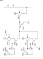
- FIG. 9 is a circuit diagram illustrating a configuration example of a pixel according to the fourth embodiment.
- a pixel 400-1 and a pixel 400-2 are an example of a plurality of pixels arranged two-dimensionally in the pixel array unit 11, and include a bias transistor 414 and a second-stage amplifier (AMP2).
- the amplifying transistor 415 is shared.
- the pixel 400-1 includes a bias transistor 414 shared with the pixel 400-2 in addition to the photodiode 411-1, the reset transistor 412-1, the amplification transistor 413-1, and the selection transistor 416-1. And an amplifying transistor 415.
- the selection transistor 416-1 is moved to the first-stage amplifier (AMP1-1) side as in the pixel 100 of FIG.
- AMP1-1-1 the first-stage amplifier
- the selection transistor 416-1 when the selection transistor 416-1 is turned on, the output of the amplification transistor 413-1 as the first-stage amplifier (AMP1-1) is read out in the two-stage state during the D-phase reading.
- the amplification transistor 415 as the eye amplifier (AMP2) is naturally activated.
- the bias transistor 414 is lowered to the vicinity of the ground (GND), so that the current from the bias transistor 414 causes the second-stage amplifier.
- the amplification transistor 415 as (AMP2) is naturally inactivated. Accordingly, in the image 400-1, the two-stage amplifier including the first-stage amplifier (AMP1-1) and the second-stage amplifier (AMP2) is automatically turned off.
- the pixel 400-2 includes a bias transistor 414 and an amplification transistor shared with the pixel 400-1. 415 is configured.
- the selection transistor 416-2 is moved to the first stage amplifier (AMP1-2) side as in the pixel 100 of FIG.
- AMP1-2 the first stage amplifier
- the selection signal (SEL) the selection signal
- the connection of the current source in the pixel 400-2 can be cut off except for the readout period.
- the selection transistor 416-2 when the selection transistor 416-2 is turned on, the output of the amplification transistor 413-2 as the first-stage amplifier (AMP1-2) is read out in two stages during the D-phase reading.
- the amplification transistor 415 as the eye amplifier (AMP2) is naturally activated.
- the bias transistor 414 is lowered to the vicinity of the ground (GND), so that the current from the bias transistor 414 causes the second-stage amplifier.
- the amplification transistor 415 as (AMP2) is naturally inactivated. Thereby, in the pixel 400-2, the two-stage amplifier including the first-stage amplifier (AMP1-2) and the second-stage amplifier (AMP2) is automatically turned off.
- the bias transistor 314 may be driven so as to be turned off.
- two-pixel sharing of the pixel 400-1 and the pixel 400-2 is illustrated as a unit of the shared pixel.
- the bias transistor includes more pixels such as 4-pixel sharing and 8-pixel sharing.
- the amplification transistor as the second-stage amplifier (AMP2) may be shared.
- the fourth embodiment has been described above.
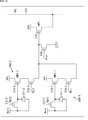
- FIG. 10 is a circuit diagram illustrating a configuration example of a pixel according to the fifth embodiment.
- a pixel 500-1 and a pixel 500-2 are configured by inverting the polarities of the photodiodes and the transistors of the two-stage amplifier in the pixels 400-1 and 400-2 shown in FIG.
- the photodiode 511-1, the amplification transistor 513-1, and the selection transistor 516-1, and the bias transistor 514 and the amplification transistor 515 shared with the pixel 500-2 are as follows. 9, the polarities of the photodiode 411-1, the amplification transistor 413-1, the selection transistor 416-1, the bias transistor 414, and the amplification transistor 415 in the pixel 400-1 in FIG. 9 are inverted.
- the selection transistor 516-1 is moved to the first-stage amplifier (AMP1-1) side similarly to the pixel 100 in FIG.
- AMP1-1-1 the first-stage amplifier
- the connection of the current source in the pixel 500-1 can be cut off except for the readout period.
- the selection transistor 516-1 when the selection transistor 516-1 is turned on, the output of the amplification transistor 513-1 serving as the first-stage amplifier (AMP1-1) is read out in two stages during the D-phase reading.
- the amplification transistor 515 as the eye amplifier (AMP2) is naturally activated.
- the selection transistor 516-1 when the selection transistor 516-1 is turned off, the bias transistor 514 is lowered to the vicinity of the ground (GND), so that the second-stage amplifier is driven by the current from the bias transistor 514.
- the amplification transistor 515 as (AMP2) is naturally inactivated.
- the two-stage amplifier including the first-stage amplifier (AMP1-1) and the second-stage amplifier (AMP2) is automatically turned off.
- the photodiode 511-2, the amplification transistor 513-2, and the selection transistor 516-2, and the bias transistor 514 and the amplification transistor 515 shared with the pixel 500-1 are illustrated in FIG.
- the polarities of the photodiode 411-2, the amplification transistor 413-2, the selection transistor 416-2, the bias transistor 414, and the amplification transistor 415 are inverted.
- the selection transistor 516-2 is moved to the first stage amplifier (AMP1-2) side as in the case of the pixel 100 in FIG.
- AMP1-2 the first stage amplifier
- the selection signal (SEL) the selection signal
- the connection of the current source in the pixel 500-2 can be cut off except for the readout period.
- the selection transistor 516-2 is turned on, and at the time of D-phase reading, the output of the amplification transistor 513-2 as the first-stage amplifier (AMP1-2)
- the amplification transistor 515 as the eye amplifier (AMP2) is naturally activated.
- the bias transistor 514 is lowered to the vicinity of the ground (GND), so that the current from the bias transistor 514 causes the second-stage amplifier.
- the amplification transistor 515 as (AMP2) is naturally inactivated. Thereby, in the pixel 500-2, the two-stage amplifier including the first-stage amplifier (AMP1-2) and the second-stage amplifier (AMP2) is automatically turned off.
- the fifth embodiment has been described above.
- FIG. 11 is a block diagram illustrating a configuration example of an electronic apparatus 1000 having a solid-state imaging device to which the technology according to the present disclosure is applied.
- the electronic device 1000 is an electronic device such as an imaging device such as a digital still camera or a video camera, or a mobile terminal device such as a smartphone or a tablet terminal.
- an imaging device such as a digital still camera or a video camera
- a mobile terminal device such as a smartphone or a tablet terminal.
- the electronic device 1000 includes a solid-state imaging device 1001, a DSP circuit 1002, a frame memory 1003, a display unit 1004, a recording unit 1005, an operation unit 1006, and a power supply unit 1007.
- the DSP circuit 1002, the frame memory 1003, the display unit 1004, the recording unit 1005, the operation unit 1006, and the power supply unit 1007 are connected to each other via a bus line 1008.
- the solid-state imaging device 1001 corresponds to the above-described solid-state imaging device 10 (FIG. 3), and the pixels 100 arranged in the pixel array unit 11 have, for example, the configuration shown in FIG. That is, in the solid-state imaging device 10, the pixel array unit 11 includes a selection transistor 116 (or a selection transistor selected from the selection transistors 216 to 516) from the second stage amplifier (AMP2) side to the first stage amplifier (AMP1). A pixel 100 (or any one of the pixels 200 to 500) moved to the side is disposed.
- the DSP circuit 1002 is a camera signal processing circuit that processes a signal supplied from the solid-state imaging device 1001.
- the DSP circuit 1002 outputs image data obtained by processing a signal from the solid-state image sensor 1001.
- the frame memory 1003 temporarily holds the image data processed by the DSP circuit 1002 in units of frames.
- the display unit 1004 includes, for example, a panel type display device such as a liquid crystal panel or an organic EL (Electro Luminescence) panel, and displays a moving image or a still image captured by the solid-state imaging device 1001.
- the recording unit 1005 records moving image or still image data captured by the solid-state imaging device 1001 on a recording medium such as a semiconductor memory or a hard disk.
- the operation unit 1006 outputs operation commands for various functions of the electronic device 1000 in accordance with user operations.
- the power supply unit 1007 appropriately supplies various power sources serving as operation power sources for the DSP circuit 1002, the frame memory 1003, the display unit 1004, the recording unit 1005, and the operation unit 1006 to these supply targets.
- the electronic device 1000 is configured as described above.
- the technology according to the present disclosure is applied to the solid-state imaging device 1001 as described above.
- the solid-state imaging device 10 in FIG. 3 can be applied to the solid-state imaging device 1001.
- the technology according to the present disclosure to the solid-state imaging device 1001, for example, it is possible to reduce the power consumption of the pixels and realize a multi-pixel, and thus it is possible to obtain a higher quality captured image.
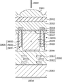
- FIG. 12 is a cross-sectional view illustrating a configuration example of a solid-state imaging device to which the technology according to the present disclosure can be applied.
- a PD (photodiode) 20019 constituting the pixel 20010 receives incident light 20001 incident from the back surface (upper surface in the drawing) side of the semiconductor substrate 20018.
- a planarizing film 20013, a CF (color filter) 20012, and a micro lens 20011 are provided above the PD 20019.
- incident light 20001 incident through each part is received by the light receiving surface 20017. Photoelectric conversion is performed.
- the n-type semiconductor region 20020 is formed as a charge accumulation region for accumulating charges (electrons).
- the n-type semiconductor region 20020 is provided inside the p-type semiconductor regions 20016 and 20041 of the semiconductor substrate 20018.
- a p-type semiconductor region 20009 having a higher impurity concentration than the back surface (upper surface) side is provided on the front surface (lower surface) side of the semiconductor substrate 20018 in the n-type semiconductor region 20020.
- PD20019 has a HAD (Hole-Accumulation Diode) structure, and a p-type semiconductor is used to suppress the occurrence of dark current at each interface between the upper surface side and the lower surface side of n-type semiconductor region 20020. Regions 20061 and 20041 are formed.
- HAD Hole-Accumulation Diode
- a pixel separation unit 20030 for electrically separating a plurality of pixels 20010 is provided, and a PD 20019 is provided in a region partitioned by the pixel separation unit 20030.
- the pixel separation unit 20030 is formed in a lattice shape so as to be interposed between a plurality of pixels 20010, for example, and the PD 20001 includes the pixel separation unit 20030. It is formed in a region partitioned by
- each PD20019 the anode is grounded, and in the solid-state imaging device, signal charges (for example, electrons) accumulated in the PD20019 are read out via a transfer Tr (MOS FET) (not shown) and the like as an electrical signal. It is output to a VSL (vertical signal line) (not shown).
- MOS FET transfer Tr
- VSL vertical signal line
- the wiring layer 20050 is provided on the surface (lower surface) opposite to the back surface (upper surface) of the semiconductor substrate 20018 where the light shielding film 20014, CF20012, microlens 20011, and the like are provided.
- the wiring layer 20050 includes a wiring 20051 and an insulating layer 20052, and the wiring 20051 is formed in the insulating layer 20052 so as to be electrically connected to each element.
- the wiring layer 20050 is a so-called multilayer wiring layer, and is formed by alternately stacking an interlayer insulating film constituting the insulating layer 20052 and the wiring 20051 a plurality of times.
- wiring 20051 wiring to the Tr for reading out charges from the PD 20019 such as the transfer Tr and wirings such as VSL are stacked via the insulating layer 20052.
- a support substrate 20061 is provided on the surface of the wiring layer 20050 opposite to the side on which the PD 20019 is provided.
- a substrate made of a silicon semiconductor having a thickness of several hundred ⁇ m is provided as the support substrate 20061.
- the light shielding film 20014 is provided on the back surface (upper surface in the drawing) side of the semiconductor substrate 20018.
- the light shielding film 20014 is configured to shield a part of incident light 20001 from the upper side of the semiconductor substrate 20018 to the lower side of the semiconductor substrate 20018.
- the light shielding film 20014 is provided above the pixel separation unit 20030 provided inside the semiconductor substrate 20018.
- the light shielding film 20014 is provided on the back surface (upper surface) of the semiconductor substrate 20018 so as to protrude in a convex shape through an insulating film 20015 such as a silicon oxide film.
- the light shielding film 20014 is not provided and is opened so that the incident light 20001 enters the PD 20019.
- the planar shape of the light shielding film 20014 is a lattice shape, and an opening through which incident light 20001 passes to the light receiving surface 20017 is formed.
- the light shielding film 20014 is formed of a light shielding material that shields light.
- a light shielding film 20014 is formed by sequentially stacking a titanium (Ti) film and a tungsten (W) film.
- the light-shielding film 20014 can be formed by sequentially stacking a titanium nitride (TiN) film and a tungsten (W) film, for example.
- the light shielding film 20014 may be covered with nitride (N) or the like.
- the light shielding film 20014 is covered with a planarizing film 20013.
- the planarization film 20013 is formed using an insulating material that transmits light.
- the pixel separation portion 20030 includes a groove portion 20031, a fixed charge film 20032, and an insulating film 20033.
- the fixed charge film 20032 is formed on the back surface (upper surface) side of the semiconductor substrate 20018 so as to cover the groove portions 20031 partitioning the plurality of pixels 20010.
- the fixed charge film 20032 is provided so as to cover the inner surface of the groove portion 20031 formed on the back surface (upper surface) side of the semiconductor substrate 20018 with a certain thickness. Then, an insulating film 20003 is provided (filled) so as to fill the inside of the groove part 20031 covered with the fixed charge film 20032.
- the fixed charge film 20032 is made of a high dielectric material having a negative fixed charge so that a positive charge (hole) accumulation region is formed at the interface with the semiconductor substrate 20018 and generation of dark current is suppressed. Is formed.
- the fixed charge film 20032 By forming the fixed charge film 20032 to have a negative fixed charge, an electric field is applied to the interface with the semiconductor substrate 20018 by the negative fixed charge, and a positive charge (hole) accumulation region is formed.
- the fixed charge film 20032 can be formed of, for example, a hafnium oxide film (HfO 2 film).
- the fixed charge film 20032 can be formed to include at least one of oxides such as hafnium, zirconium, aluminum, tantalum, titanium, magnesium, yttrium, and a lanthanoid element.
- the technology according to the present disclosure can be applied to the solid-state imaging device as described above.
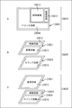
- FIG. 13 is a diagram illustrating an outline of a configuration example of a stacked solid-state imaging device to which the technology according to the present disclosure can be applied.
- FIG. 13A shows a schematic configuration example of a non-stacked solid-state imaging device.
- the solid-state imaging device 23010 includes a single die (semiconductor substrate) 23011 as illustrated in FIG.
- the die 23011 is mounted with a pixel region 23012 in which pixels are arranged in an array, a control circuit 23013 for driving the pixel and other various controls, and a logic circuit 23014 for signal processing.
- the solid-state imaging device 23020 is configured as a single semiconductor chip in which two dies, a sensor die 23021 and a logic die 23024, are stacked and electrically connected.
- the sensor die 23021 has a pixel region 23012 and a control circuit 23013 mounted thereon, and the logic die 23024 has a logic circuit 23014 including a signal processing circuit for performing signal processing.
- the sensor die 23021 has a pixel region 23012 mounted thereon
- the logic die 23024 has a control circuit 23013 and a logic circuit 23014 mounted thereon.
- FIG. 14 is a cross-sectional view illustrating a first configuration example of a stacked solid-state imaging device 23020.
- a PD photodiode
- an FD floating diffusion
- a Tr MOS FET
- a Tr serving as a control circuit 23013 are formed.
- a wiring layer 23101 having a plurality of layers, in this example, three layers of wirings 23110 is formed on the sensor die 23021.
- the control circuit 23013 (being Tr) can be configured in the logic die 23024 instead of the sensor die 23021.
- a Tr constituting the logic circuit 23014 is formed. Further, the logic die 23024 is formed with a wiring layer 23161 including a plurality of layers 23170 in this example. In addition, a connection hole 23171 having an insulating film 23172 formed on the inner wall surface is formed in the logic die 23024, and a connection conductor 23173 connected to the wiring 23170 and the like is embedded in the connection hole 23171.
- the sensor die 23021 and the logic die 23024 are bonded together so that the wiring layers 23101 and 23161 face each other, thereby forming a stacked solid-state imaging device 23020 in which the sensor die 23021 and the logic die 23024 are stacked.
- a film 23191 such as a protective film is formed on a surface where the sensor die 23021 and the logic die 23024 are bonded.
- connection hole 23111 is formed which penetrates the sensor die 23021 from the back side (side where light enters the PD) (upper side) of the sensor die 23021 and reaches the uppermost wiring 23170 of the logic die 23024.
- a connection hole 23121 is formed in the sensor die 23021 in the vicinity of the connection hole 23111 so as to reach the first layer wiring 23110 from the back surface side of the sensor die 23021.
- An insulating film 23112 is formed on the inner wall surface of the connection hole 23111, and an insulating film 23122 is formed on the inner wall surface of the connection hole 23121.
- Connection conductors 23113 and 23123 are embedded in the connection holes 23111 and 23121, respectively.
- connection conductor 23113 and the connection conductor 23123 are electrically connected on the back side of the sensor die 23021, whereby the sensor die 23021 and the logic die 23024 are connected to the wiring layer 23101, the connection hole 23121, the connection hole 23111, and the wiring layer. It is electrically connected through 23161.
- FIG. 15 is a cross-sectional view illustrating a second configuration example of the stacked solid-state imaging device 23020.
- the sensor die 23021 (the wiring layer 23101 (the wiring 23110)) and the logic die 23024 (the wiring layer 23161 (the wiring thereof) are formed by one connection hole 23211 formed in the sensor die 23021. 23170)) are electrically connected.
- connection hole 23211 is formed so as to penetrate the sensor die 23021 from the back side of the sensor die 23021 to reach the uppermost layer wiring 23170 of the logic die 23024 and to reach the uppermost layer wiring 23110 of the sensor die 23021. Is done.
- An insulating film 23212 is formed on the inner wall surface of the connection hole 23211, and a connection conductor 23213 is embedded in the connection hole 23211.
- the sensor die 23021 and the logic die 23024 are electrically connected through the two connection holes 23111 and 23121.
- the sensor die 23021 and the logic die 23024 are connected through the single connection hole 23211. Electrically connected.
- FIG. 16 is a cross-sectional view illustrating a third configuration example of the stacked solid-state imaging device 23020.
- the solid-state imaging device 23020 in FIG. 16 has a surface on which the sensor die 23021 and the logic die 23024 are bonded to each other in that a film 23191 such as a protective film is not formed on the surface on which the sensor die 23021 and the logic die 23024 are bonded. 14 differs from the case of FIG. 14 in which a film 23191 such as a protective film is formed.
- the sensor die 23021 and the logic die 23024 are superposed so that the wirings 23110 and 23170 are in direct contact with each other and heated while applying a required weight, thereby directly joining the wirings 23110 and 23170. Composed.
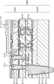
- FIG. 17 is a cross-sectional view illustrating another configuration example of the stacked solid-state imaging device to which the technology according to the present disclosure can be applied.
- the solid-state imaging device 23401 has a three-layer stacked structure in which three dies of a sensor die 23411, a logic die 23412, and a memory die 23413 are stacked.
- the memory die 23413 includes, for example, a memory circuit that stores data temporarily necessary for signal processing performed by the logic die 23412.
- a logic die 23412 and a memory die 23413 are stacked in that order under the sensor die 23411. 23411 can be laminated.
- the sensor die 23411 is formed with a PD serving as a photoelectric conversion portion of the pixel and a source / drain region of the pixel Tr.
- a gate electrode is formed around the PD via a gate insulating film, and a pixel Tr 23421 and a pixel Tr 23422 are formed by a source / drain region paired with the gate electrode.
- a pixel Tr 23421 adjacent to the PD is a transfer Tr, and one of a pair of source / drain regions constituting the pixel Tr 23421 is an FD.
- an interlayer insulating film is formed in the sensor die 23411, and a connection hole is formed in the interlayer insulating film.
- a connection hole is formed in the interlayer insulating film.
- a wiring layer 23433 having a plurality of layers of wirings 23432 connected to the respective connection conductors 23431 is formed in the sensor die 23411.
- an aluminum pad 23434 serving as an electrode for external connection is formed in the lowermost layer of the wiring layer 23433 of the sensor die 23411.
- the aluminum pad 23434 is formed at a position closer to the bonding surface 23440 with the logic die 23412 than to the wiring 23432.
- the aluminum pad 23434 is used as one end of wiring related to signal input / output with the outside.
- a contact 23441 used for electrical connection with the logic die 23412 is formed on the sensor die 23411.
- the contact 23441 is connected to the contact 23451 of the logic die 23412 and is also connected to the aluminum pad 23442 of the sensor die 23411.
- a pad hole 23443 is formed so as to reach the aluminum pad 23442 from the back side (upper side) of the sensor die 23411.
- the technology according to the present disclosure can be applied to the solid-state imaging device as described above.
- the technology (this technology) according to the present disclosure can be applied to various products.
- the technology according to the present disclosure is realized as a device that is mounted on any type of mobile body such as an automobile, an electric vehicle, a hybrid electric vehicle, a motorcycle, a bicycle, personal mobility, an airplane, a drone, a ship, and a robot. May be.
- FIG. 18 is a block diagram illustrating a schematic configuration example of a vehicle control system that is an example of a mobile control system to which the technology according to the present disclosure can be applied.
- the vehicle control system 12000 includes a plurality of electronic control units connected via a communication network 12001.
- the vehicle control system 12000 includes a drive system control unit 12010, a body system control unit 12020, a vehicle exterior information detection unit 12030, a vehicle interior information detection unit 12040, and an integrated control unit 12050.
- a microcomputer 12051, a sound image output unit 12052, and an in-vehicle network I / F (Interface) 12053 are illustrated as a functional configuration of the integrated control unit 12050.
- the drive system control unit 12010 controls the operation of the device related to the drive system of the vehicle according to various programs.
- the drive system control unit 12010 includes a driving force generator for generating a driving force of a vehicle such as an internal combustion engine or a driving motor, a driving force transmission mechanism for transmitting the driving force to wheels, and a steering angle of the vehicle. It functions as a control device such as a steering mechanism that adjusts and a braking device that generates a braking force of the vehicle.
- the body system control unit 12020 controls the operation of various devices mounted on the vehicle body according to various programs.
- the body system control unit 12020 functions as a keyless entry system, a smart key system, a power window device, or a control device for various lamps such as a headlamp, a back lamp, a brake lamp, a blinker, or a fog lamp.
- the body control unit 12020 can be input with radio waves transmitted from a portable device that substitutes for a key or signals from various switches.
- the body system control unit 12020 receives input of these radio waves or signals, and controls a door lock device, a power window device, a lamp, and the like of the vehicle.
- the vehicle outside information detection unit 12030 detects information outside the vehicle on which the vehicle control system 12000 is mounted.
- the imaging unit 12031 is connected to the vehicle exterior information detection unit 12030.
- the vehicle exterior information detection unit 12030 causes the imaging unit 12031 to capture an image outside the vehicle and receives the captured image.
- the vehicle outside information detection unit 12030 may perform an object detection process or a distance detection process such as a person, a car, an obstacle, a sign, or a character on a road surface based on the received image.
- the imaging unit 12031 is an optical sensor that receives light and outputs an electrical signal corresponding to the amount of received light.
- the imaging unit 12031 can output an electrical signal as an image, or can output it as distance measurement information. Further, the light received by the imaging unit 12031 may be visible light or invisible light such as infrared rays.
- the vehicle interior information detection unit 12040 detects vehicle interior information.
- a driver state detection unit 12041 that detects a driver's state is connected to the in-vehicle information detection unit 12040.
- the driver state detection unit 12041 includes, for example, a camera that images the driver, and the vehicle interior information detection unit 12040 determines the degree of fatigue or concentration of the driver based on the detection information input from the driver state detection unit 12041. It may be calculated or it may be determined whether the driver is asleep.
- the microcomputer 12051 calculates a control target value of the driving force generator, the steering mechanism, or the braking device based on the information inside / outside the vehicle acquired by the vehicle outside information detection unit 12030 or the vehicle interior information detection unit 12040, and the drive system control unit A control command can be output to 12010.
- the microcomputer 12051 realizes ADAS (Advanced Driver Assistance System) functions including vehicle collision avoidance or impact mitigation, following traveling based on inter-vehicle distance, vehicle speed maintenance traveling, vehicle collision warning, or vehicle lane departure warning. It is possible to perform cooperative control for the purpose.
- ADAS Advanced Driver Assistance System
- the microcomputer 12051 controls the driving force generator, the steering mechanism, the braking device, and the like based on the information around the vehicle acquired by the vehicle exterior information detection unit 12030 or the vehicle interior information detection unit 12040. It is possible to perform cooperative control for the purpose of automatic driving that autonomously travels without depending on the operation.
- the microcomputer 12051 can output a control command to the body system control unit 12020 based on information outside the vehicle acquired by the vehicle outside information detection unit 12030.
- the microcomputer 12051 controls the headlamp according to the position of the preceding vehicle or the oncoming vehicle detected by the outside information detection unit 12030, and performs cooperative control for the purpose of anti-glare, such as switching from a high beam to a low beam. It can be carried out.
- the sound image output unit 12052 transmits an output signal of at least one of sound and image to an output device capable of visually or audibly notifying information to a vehicle occupant or the outside of the vehicle.
- an audio speaker 12061, a display unit 12062, and an instrument panel 12063 are illustrated as output devices.
- the display unit 12062 may include at least one of an on-board display and a head-up display, for example.
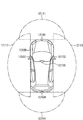
- FIG. 19 is a diagram illustrating an example of an installation position of the imaging unit 12031.
- the imaging unit 12031 includes imaging units 12101, 12102, 12103, 12104, and 12105.
- the imaging units 12101, 12102, 12103, 12104, and 12105 are provided, for example, at positions such as a front nose, a side mirror, a rear bumper, a back door, and an upper part of a windshield in the vehicle interior of the vehicle 12100.
- the imaging unit 12101 provided in the front nose and the imaging unit 12105 provided in the upper part of the windshield in the vehicle interior mainly acquire an image in front of the vehicle 12100.
- the imaging units 12102 and 12103 provided in the side mirror mainly acquire an image of the side of the vehicle 12100.
- the imaging unit 12104 provided in the rear bumper or the back door mainly acquires an image behind the vehicle 12100.
- the imaging unit 12105 provided on the upper part of the windshield in the passenger compartment is mainly used for detecting a preceding vehicle or a pedestrian, an obstacle, a traffic light, a traffic sign, a lane, or the like.
- FIG. 19 shows an example of the shooting range of the imaging units 12101 to 12104.
- the imaging range 12111 indicates the imaging range of the imaging unit 12101 provided in the front nose
- the imaging ranges 12112 and 12113 indicate the imaging ranges of the imaging units 12102 and 12103 provided in the side mirrors, respectively
- the imaging range 12114 The imaging range of the imaging part 12104 provided in the rear bumper or the back door is shown. For example, by superimposing the image data captured by the imaging units 12101 to 12104, an overhead image when the vehicle 12100 is viewed from above is obtained.
- At least one of the imaging units 12101 to 12104 may have a function of acquiring distance information.
- at least one of the imaging units 12101 to 12104 may be a stereo camera including a plurality of imaging elements, or may be an imaging element having pixels for phase difference detection.
- the microcomputer 12051 based on the distance information obtained from the imaging units 12101 to 12104, the distance to each three-dimensional object in the imaging range 12111 to 12114 and the temporal change in this distance (relative speed with respect to the vehicle 12100).
- a solid object that travels at a predetermined speed (for example, 0 km / h or more) in the same direction as the vehicle 12100, particularly the closest three-dimensional object on the traveling path of the vehicle 12100. it can.
- the microcomputer 12051 can set an inter-vehicle distance to be secured in advance before the preceding vehicle, and can perform automatic brake control (including follow-up stop control), automatic acceleration control (including follow-up start control), and the like.
- automatic brake control including follow-up stop control
- automatic acceleration control including follow-up start control
- cooperative control for the purpose of autonomous driving or the like autonomously traveling without depending on the operation of the driver can be performed.
- the microcomputer 12051 converts the three-dimensional object data related to the three-dimensional object to other three-dimensional objects such as a two-wheeled vehicle, a normal vehicle, a large vehicle, a pedestrian, and a utility pole based on the distance information obtained from the imaging units 12101 to 12104. It can be classified and extracted and used for automatic avoidance of obstacles.
- the microcomputer 12051 identifies obstacles around the vehicle 12100 as obstacles that are visible to the driver of the vehicle 12100 and obstacles that are difficult to see.
- the microcomputer 12051 determines the collision risk indicating the risk of collision with each obstacle, and when the collision risk is equal to or higher than the set value and there is a possibility of collision, the microcomputer 12051 is connected via the audio speaker 12061 or the display unit 12062. By outputting an alarm to the driver and performing forced deceleration or avoidance steering via the drive system control unit 12010, driving assistance for collision avoidance can be performed.
- At least one of the imaging units 12101 to 12104 may be an infrared camera that detects infrared rays.
- the microcomputer 12051 can recognize a pedestrian by determining whether a pedestrian is present in the captured images of the imaging units 12101 to 12104. Such pedestrian recognition is, for example, whether or not the user is a pedestrian by performing a pattern matching process on a sequence of feature points indicating the outline of an object and a procedure for extracting feature points in the captured images of the imaging units 12101 to 12104 as infrared cameras. It is carried out by the procedure for determining.
- the audio image output unit 12052 When the microcomputer 12051 determines that there is a pedestrian in the captured images of the imaging units 12101 to 12104 and recognizes the pedestrian, the audio image output unit 12052 has a rectangular contour line for emphasizing the recognized pedestrian.
- the display unit 12062 is controlled so as to be superimposed and displayed.
- voice image output part 12052 may control the display part 12062 so that the icon etc. which show a pedestrian may be displayed on a desired position.
- the technology according to the present disclosure can be applied to the imaging unit 12101 among the configurations described above.
- the solid-state imaging device 10 in FIG. 3 can be applied to the imaging unit 12101.
- the technology (this technology) according to the present disclosure can be applied to various products.
- the technology according to the present disclosure may be applied to an endoscopic surgery system.
- FIG. 20 is a block diagram illustrating an example of a schematic configuration of a patient in-vivo information acquisition system using a capsule endoscope to which the technology (present technology) according to the present disclosure can be applied.
- the in-vivo information acquisition system 10001 includes a capsule endoscope 10100 and an external control device 10200.
- the capsule endoscope 10100 is swallowed by the patient at the time of examination.
- the capsule endoscope 10100 has an imaging function and a wireless communication function, and moves inside the organ such as the stomach and the intestine by peristaltic motion or the like until it is spontaneously discharged from the patient.
- Images (hereinafter also referred to as in-vivo images) are sequentially captured at predetermined intervals, and information about the in-vivo images is sequentially wirelessly transmitted to the external control device 10200 outside the body.
- the external control device 10200 comprehensively controls the operation of the in-vivo information acquisition system 10001. Further, the external control device 10200 receives information about the in-vivo image transmitted from the capsule endoscope 10100 and, based on the received information about the in-vivo image, displays the in-vivo image on the display device (not shown). The image data for displaying is generated.
- an in-vivo image obtained by imaging the inside of the patient's body can be obtained at any time in this manner until the capsule endoscope 10100 is swallowed and discharged.
- the capsule endoscope 10100 includes a capsule-type casing 10101.
- a light source unit 10111 In the casing 10101, a light source unit 10111, an imaging unit 10112, an image processing unit 10113, a wireless communication unit 10114, a power supply unit 10115, and a power supply unit 10116 and the control unit 10117 are stored.
- the light source unit 10111 includes a light source such as an LED (light-emitting diode), and irradiates the imaging field of the imaging unit 10112 with light.
- a light source such as an LED (light-emitting diode)
- the image capturing unit 10112 includes an image sensor and an optical system including a plurality of lenses provided in front of the image sensor. Reflected light (hereinafter referred to as observation light) of light irradiated on the body tissue to be observed is collected by the optical system and enters the image sensor. In the imaging unit 10112, in the imaging element, the observation light incident thereon is photoelectrically converted, and an image signal corresponding to the observation light is generated. The image signal generated by the imaging unit 10112 is provided to the image processing unit 10113.
- the image processing unit 10113 is configured by a processor such as a CPU (Central Processing Unit) or a GPU (Graphics Processing Unit), and performs various types of signal processing on the image signal generated by the imaging unit 10112.
- the image processing unit 10113 provides the radio communication unit 10114 with the image signal subjected to signal processing as RAW data.
- the wireless communication unit 10114 performs predetermined processing such as modulation processing on the image signal that has been subjected to signal processing by the image processing unit 10113, and transmits the image signal to the external control apparatus 10200 via the antenna 10114A.
- the wireless communication unit 10114 receives a control signal related to drive control of the capsule endoscope 10100 from the external control device 10200 via the antenna antenna 10114A.
- the wireless communication unit 10114 provides a control signal received from the external control device 10200 to the control unit 10117.
- the power feeding unit 10115 includes a power receiving antenna coil, a power regeneration circuit that regenerates power from a current generated in the antenna coil, a booster circuit, and the like. In the power feeding unit 10115, electric power is generated using a so-called non-contact charging principle.
- the power supply unit 10116 is composed of a secondary battery, and stores the electric power generated by the power supply unit 10115.
- FIG. 20 in order to avoid complication of the drawing, illustration of an arrow or the like indicating a power supply destination from the power supply unit 10116 is omitted, but the power stored in the power supply unit 10116 is the light source unit 10111.
- the imaging unit 10112, the image processing unit 10113, the wireless communication unit 10114, and the control unit 10117 can be used for driving them.
- the control unit 10117 includes a processor such as a CPU, and a control signal transmitted from the external control device 10200 to drive the light source unit 10111, the imaging unit 10112, the image processing unit 10113, the wireless communication unit 10114, and the power feeding unit 10115. Control accordingly.
- a processor such as a CPU
- the external control device 10200 is constituted by a CPU, a processor such as a GPU, or a microcomputer or a control board in which a processor and a storage element such as a memory are mounted.
- the external control device 10200 controls the operation of the capsule endoscope 10100 by transmitting a control signal to the control unit 10117 of the capsule endoscope 10100 via the antenna 10200A.
- the capsule endoscope 10100 for example, the light irradiation condition for the observation target in the light source unit 10111 can be changed by a control signal from the external control device 10200.
- an imaging condition for example, a frame rate or an exposure value in the imaging unit 10112
- the contents of processing in the image processing unit 10113 and the conditions (for example, the transmission interval, the number of transmission images, etc.) by which the wireless communication unit 10114 transmits an image signal may be changed by a control signal from the external control device 10200. .
- the external control device 10200 performs various image processing on the image signal transmitted from the capsule endoscope 10100, and generates image data for displaying the captured in-vivo image on the display device.
- the image processing includes, for example, development processing (demosaic processing), image quality enhancement processing (band enhancement processing, super-resolution processing, NR (Noise reduction) processing and / or camera shake correction processing, etc.), and / or enlargement processing ( Various signal processing such as electronic zoom processing can be performed.
- the external control device 10200 controls driving of the display device to display an in-vivo image captured based on the generated image data. Alternatively, the external control device 10200 may cause the generated image data to be recorded on a recording device (not shown) or may be printed out on a printing device (not shown).
- the technology according to the present disclosure can be applied to the imaging unit 10112 among the configurations described above.
- the solid-state imaging device 10 in FIG. 3 can be applied to the imaging unit 10112.
- the technique according to the present disclosure to the imaging unit 10112, for example, by suppressing the power consumption of the pixels and realizing a large number of pixels, a higher-quality captured image can be obtained.
- the technology according to the present disclosure can take the following configurations.
- a photoelectric conversion unit A reset transistor that resets the photoelectric conversion unit in response to a reset signal; A first amplification transistor for amplifying a signal from the photoelectric conversion unit; A selection transistor that selects a signal from the first amplification transistor in response to a selection signal; A second amplification transistor for amplifying a signal from the selection transistor and applying the amplified signal to a vertical signal line; A pixel array unit, the pixel having a bias transistor connected to the selection transistor and the second amplification transistor and functioning as a current source, in which the pixels from which logarithmic characteristic output signals are obtained are arranged in a matrix , The first amplification transistor and the second amplification transistor are connected to a power supply voltage, respectively.
- the gate is connected to the photoelectric conversion unit, Its source is connected to the drain of the selection transistor, Its drain is connected to the power supply voltage, In the second amplification transistor, Its gate is connected to the source of the selection transistor, Its source is connected to the vertical signal line, The drain is connected to the power supply voltage.
- the solid-state imaging device according to (1) In the bias transistor, Its source is grounded The drain is connected to the source of the selection transistor and the gate of the second amplification transistor.
- the reset transistor is driven so as to be in an ON state at the time of reading a reset level in a shutter driving period before the exposure period and a reading period after the exposure period, The solid-state imaging device according to (3), wherein the selection transistor is driven to be in an on state during the readout period.
- the reset transistor is driven so as to be in an ON state at the time of reading a reset level in a shutter driving period before the exposure period and a reading period after the exposure period, The selection transistor is driven to be in an on state during the readout period, The solid-state imaging device according to (3), wherein the bias transistor is driven to be in an off state except for the readout period.
- Polarities of the photoelectric conversion unit, the first amplification transistor, the selection transistor, the second amplification transistor, and the bias transistor are inverted.
- the solid-state imaging device is a logarithmic sensor in a solar cell mode.
- the first amplification transistor and the second amplification transistor are electronic devices each including a solid-state imaging device connected to a power supply voltage.
- the first amplifying transistor and the second amplifying transistor are respectively connected to a power supply voltage and are driving methods of a solid-state imaging device, Drive so that the reset transistor is turned on in the shutter driving period before the exposure period, In a readout period after the exposure period, the selection transistor is driven to be turned on, A driving method of driving so that the reset transistor is turned on at the time of reading the reset
- a photoelectric conversion unit A reset transistor that resets the photoelectric conversion unit in response to a reset signal; A first amplification transistor for amplifying a signal from the photoelectric conversion unit; A selection transistor that selects a signal from the first amplification transistor in response to a selection signal; A second amplifying transistor for amplifying a signal from the selection transistor and applying the signal to a vertical signal line; a bias transistor connected to the selection transistor and the second amplifying transistor and functioning as a current source; A pixel array section in which the pixels from which logarithmic characteristic output signals are obtained are arranged in a matrix, The first amplifying transistor and the second amplifying transistor are respectively connected to a power supply voltage and are driving methods of a solid-state imaging device, Drive so that the reset transistor is turned on in the shutter driving period before the exposure period, In a readout period after the exposure period, the selection transistor is driven to be turned on, When the reset level is read during the read period, the reset transistor is driven to be in an on state, A driving method of driving so
- 10 solid-state imaging device 11 pixel array section, 100, 200 pixels, 111, 211 photodiode, 112, 212 reset transistor, 113, 213 amplification transistor, 114, 214 bias transistor, 115, 215 amplification transistor, 116, 216 selection transistor , 121, 221 vertical signal line, 300 pixels, 311 photodiode, 312 reset transistor, 313 amplification transistor, 314 bias transistor, 315 amplification transistor, 316 selection transistor, 321 vertical signal line, 400-1, 400-2, 500- 1,500-2 pixels, 411-1, 411-2, 511-1, 511-2, photodiode, 4 2-1, 412-2, 512-1, 512-2 reset transistor, 413-1, 413-2, 513-1, 513-2 amplification transistor, 414, 514 bias transistor, 415, 515 amplification transistor, 416- 1, 416-2, 516-1, 516-2, select transistor, 421, 521, vertical signal line, 1000 electronic device, 1001, solid-state image sensor
Landscapes
- Engineering & Computer Science (AREA)
- Multimedia (AREA)
- Signal Processing (AREA)
- Physics & Mathematics (AREA)
- Nonlinear Science (AREA)
- Solid State Image Pick-Up Elements (AREA)
- Transforming Light Signals Into Electric Signals (AREA)
Abstract
本開示は、画素の消費電力を抑制して、多画素化を実現することができるようにする固体撮像装置、電子機器、及び駆動方法に関する。 光電変換部と、リセット信号に応じて、光電変換部をリセットするリセットトランジスタと、光電変換部からの信号を増幅する第1の増幅トランジスタと、選択信号に応じて、第1の増幅トランジスタからの信号を選択する選択トランジスタと、選択トランジスタからの信号を増幅し、垂直信号線に印加する第2の増幅トランジスタと、電流源として機能するバイアストランジスタとを有する画素であって、対数特性の出力信号が得られる画素を行列状に配置した画素アレイ部を備え、第1の増幅トランジスタと、第2の増幅トランジスタは、電源電圧とそれぞれ接続される固体撮像装置が提供される。本開示に係る技術は、例えば、太陽電池モードの対数センサに適用することができる。
Description
本開示は、固体撮像装置、電子機器、及び駆動方法に関し、特に、画素の消費電力を抑制して、多画素化を実現することができるようにした固体撮像装置、電子機器、及び駆動方法に関する。
フォトダイオードを、太陽電池と同様に、開回路で動作させて、出力電圧を計測する対数センサ(Logarithmic Image Sensor)が知られている(例えば、非特許文献1参照)。
このような太陽電池モードの対数センサは、PNジャンクションの順方向に電流を流したときに生じる電位差、すなわち、電圧が電流の対数と比例する関係を用いている。この順方向の電流を、光電変換によって発生した光電流に置き換えて、PNジャンクションの順方向の電圧をモニタすれば、それは、光電流を対数圧縮した信号となる。
2011年 International Image Sensor Workshop (IISW), 2011/6/9, 講演 R35, "A 768x576 Logarithmic Image Sensor with Photodiode in Solar Cell mode" Yang Ni, YiMing Zhu, Bogdan Arion New Imaging Technologies SA
ところで、太陽電池モードの対数センサでは、フォトダイオードの過渡応答に垂直信号線(VSL)の電位変動を重畳しないようにするために、各画素の構造として、2段のアンプで構成される2段アンプ構造を採用するのが一般的である。
このような2段アンプ構造を採用する場合には、画素内に、電流源を搭載する必要が出てくる。しかしながら、このように、画素内に、電流源を搭載すると、定常的に貫通電流が流れることになり、消費電力が大きくなるとともに、多画素化の阻害要因にもなる。
本開示はこのような状況に鑑みてなされたものであり、太陽電池モードの対数センサにおいて、画素の消費電力を抑制して、多画素化を実現することができるようにするものである。
本開示の一側面の固体撮像装置は、光電変換部と、リセット信号に応じて、前記光電変換部をリセットするリセットトランジスタと、前記光電変換部からの信号を増幅する第1の増幅トランジスタと、選択信号に応じて、前記第1の増幅トランジスタからの信号を選択する選択トランジスタと、前記選択トランジスタからの信号を増幅し、垂直信号線に印加する第2の増幅トランジスタと、前記選択トランジスタ及び前記第2の増幅トランジスタと接続され、電流源として機能するバイアストランジスタとを有する画素であって、対数特性の出力信号が得られる前記画素を行列状に配置した画素アレイ部を備え、前記第1の増幅トランジスタと、前記第2の増幅トランジスタは、電源電圧とそれぞれ接続される固体撮像装置である。
本開示の一側面の電子機器は、光電変換部と、リセット信号に応じて、前記光電変換部をリセットするリセットトランジスタと、前記光電変換部からの信号を増幅する第1の増幅トランジスタと、選択信号に応じて、前記第1の増幅トランジスタからの信号を選択する選択トランジスタと、前記選択トランジスタからの信号を増幅し、垂直信号線に印加する第2の増幅トランジスタと、前記選択トランジスタ及び前記第2の増幅トランジスタと接続され、電流源として機能するバイアストランジスタとを有する画素であって、対数特性の出力信号が得られる前記画素を行列状に配置した画素アレイ部を備え、前記第1の増幅トランジスタと、前記第2の増幅トランジスタは、電源電圧とそれぞれ接続される固体撮像装置を搭載した電子機器である。
本開示の一側面の固体撮像装置及び電子機器においては、光電変換部と、リセット信号に応じて、前記光電変換部をリセットするリセットトランジスタと、前記光電変換部からの信号を増幅する第1の増幅トランジスタと、選択信号に応じて、前記第1の増幅トランジスタからの信号を選択する選択トランジスタと、前記選択トランジスタからの信号を増幅し、垂直信号線に印加する第2の増幅トランジスタと、前記選択トランジスタ及び前記第2の増幅トランジスタと接続され、電流源として機能するバイアストランジスタとを有する画素であって、対数特性の出力信号が得られる前記画素を行列状に配置した画素アレイ部が設けられ、前記第1の増幅トランジスタと、前記第2の増幅トランジスタは、電源電圧とそれぞれ接続されるように構成される。
なお、本開示の一側面の固体撮像装置又は電子機器は、独立した装置であってもよいし、1つの装置を構成している内部ブロックであってもよい。
本開示の一側面の駆動方法は、光電変換部と、リセット信号に応じて、前記光電変換部をリセットするリセットトランジスタと、前記光電変換部からの信号を増幅する第1の増幅トランジスタと、選択信号に応じて、前記第1の増幅トランジスタからの信号を選択する選択トランジスタと、前記選択トランジスタからの信号を増幅し、垂直信号線に印加する第2の増幅トランジスタと、前記選択トランジスタ及び前記第2の増幅トランジスタと接続され、電流源として機能するバイアストランジスタとを有する画素であって、対数特性の出力信号が得られる前記画素を行列状に配置した画素アレイ部を備え、前記第1の増幅トランジスタと、前記第2の増幅トランジスタは、電源電圧とそれぞれ接続される固体撮像装置の駆動方法であって、露光期間よりも前のシャッタ駆動期間に、前記リセットトランジスタがオン状態となるように駆動し、前記露光期間よりも後の読み出し期間に、前記選択トランジスタがオン状態となるように駆動し、前記読み出し期間のリセットレベルの読み出し時に、前記リセットトランジスタがオン状態となるように駆動する駆動方法である。
本開示の一側面の駆動方法においては、露光期間よりも前のシャッタ駆動期間に、リセットトランジスタがオン状態となるように駆動され、露光期間よりも後の読み出し期間に、選択トランジスタがオン状態となるように駆動され、読み出し期間のリセットレベルの読み出し時に、リセットトランジスタがオン状態となるように駆動される。
本開示の一側面の駆動方法は、光電変換部と、リセット信号に応じて、前記光電変換部をリセットするリセットトランジスタと、前記光電変換部からの信号を増幅する第1の増幅トランジスタと、選択信号に応じて、前記第1の増幅トランジスタからの信号を選択する選択トランジスタと、前記選択トランジスタからの信号を増幅し、垂直信号線に印加する第2の増幅トランジスタと、前記選択トランジスタ及び前記第2の増幅トランジスタと接続され、電流源として機能するバイアストランジスタとを有する画素であって、対数特性の出力信号が得られる前記画素を行列状に配置した画素アレイ部を備え、前記第1の増幅トランジスタと、前記第2の増幅トランジスタは、電源電圧とそれぞれ接続される固体撮像装置の駆動方法であって、露光期間よりも前のシャッタ駆動期間に、前記リセットトランジスタがオン状態となるように駆動し、前記露光期間よりも後の読み出し期間に、前記選択トランジスタがオン状態となるように駆動し、前記読み出し期間のリセットレベルの読み出し時に、前記リセットトランジスタがオン状態となるように駆動し、前記読み出し期間を除いて、前記バイアストランジスタがオフ状態となるように駆動する駆動方法である。
本開示の一側面の駆動方法においては、露光期間よりも前のシャッタ駆動期間に、リセットトランジスタがオン状態となるように駆動され、露光期間よりも後の読み出し期間に、選択トランジスタがオン状態となるように駆動され、読み出し期間のリセットレベルの読み出し時に、リセットトランジスタがオン状態となるように駆動され、読み出し期間を除いて、バイアストランジスタがオフ状態となるように駆動される。
本開示の一側面によれば、画素の消費電力を抑制して、多画素化を実現することができる。
なお、ここに記載された効果は必ずしも限定されるものではなく、本開示中に記載されたいずれかの効果であってもよい。
以下、図面を参照しながら本開示に係る技術(本技術)の実施の形態について説明する。なお、説明は以下の順序で行うものとする。
1.本開示に係る技術の概要
2.本開示に係る技術を適用した固体撮像装置の構成例
3.第1の実施の形態:基本構成
4.第2の実施の形態:Biasのゲート入力電圧を駆動した構成
5.第3の実施の形態:PDと2段アンプのトランジスタの極性を反転した構成
6.第4の実施の形態:Bias,AMP2を、複数の画素で共有した構成
7.第5の実施の形態:共有画素で、PDと2段アンプのトランジスタの極性を反転した構成
8.本開示に係る技術を適用した固体撮像装置を有する電子機器の構成例
9.本開示に係る技術を適用し得る固体撮像装置の断面構成例
10.本開示に係る技術を適用し得る積層型の固体撮像装置の構成例
11.移動体への応用例
12.体内情報取得システムへの応用例
2.本開示に係る技術を適用した固体撮像装置の構成例
3.第1の実施の形態:基本構成
4.第2の実施の形態:Biasのゲート入力電圧を駆動した構成
5.第3の実施の形態:PDと2段アンプのトランジスタの極性を反転した構成
6.第4の実施の形態:Bias,AMP2を、複数の画素で共有した構成
7.第5の実施の形態:共有画素で、PDと2段アンプのトランジスタの極性を反転した構成
8.本開示に係る技術を適用した固体撮像装置を有する電子機器の構成例
9.本開示に係る技術を適用し得る固体撮像装置の断面構成例
10.本開示に係る技術を適用し得る積層型の固体撮像装置の構成例
11.移動体への応用例
12.体内情報取得システムへの応用例
<1.本開示に係る技術の概要>
(対数センサの画素の構成)
図1は、一般的な太陽電池モードの対数センサの画素の構成を示す図である。
図1は、一般的な太陽電池モードの対数センサの画素の構成を示す図である。
なお、図1に示した一般的な対数センサの画素900は、CMOS(Complementary Metal Oxide Semiconductor)イメージセンサ等の固体撮像装置において、画素アレイ部に行列状に配置される複数の画素のうちの1つの画素に相当するものである。
図1において、一般的な対数センサの画素900は、フォトダイオード911、リセットトランジスタ912、増幅トランジスタ913、バイアストランジスタ914、増幅トランジスタ915、及び選択トランジスタ916を含んで構成される。
フォトダイオード911は、n型とp型の半導体領域からなる光電変換部である。リセットトランジスタ912は、そのゲート電極に印加されるリセット信号(RST)のオンオフに応じて、フォトダイオード911のリセットを制御する。
増幅トランジスタ913は、そのゲート電極に印加されるフォトダイオード911からの信号を増幅し、増幅トランジスタ915に出力する。バイアストランジスタ914は、電流源として機能する。
増幅トランジスタ915は、そのゲート電極に印加されるフォトダイオード911からの信号を増幅し、選択トランジスタ916に出力する。選択トランジスタ916は、そのゲート電極に印加される選択信号(SEL)のオンオフに応じて、増幅トランジスタ915からの信号を、垂直信号線921に出力する。
このように、一般的な対数センサの画素900においては、フォトダイオード911の過渡応答に垂直信号線(VSL)921の電位変動を重畳しないようにするために、初段アンプ(AMP1)としての増幅トランジスタ913と、2段目アンプ(AMP2)としての増幅トランジスタ915とからなる2段アンプ構造を採用している。
また、このような2段アンプ構造を採用した場合には、画素900内に、電流源として機能するバイアストランジスタ914を搭載する必要が出てくるが、バイアストランジスタ914を搭載することで、画素900内には、定常的にバイアス電流IBiasが流れることになる。
(対数センサの画素の駆動方法)
図2は、一般的な太陽電池モードの対数センサの画素900(図1)の駆動方法を説明するタイミングチャートである。
図2は、一般的な太陽電池モードの対数センサの画素900(図1)の駆動方法を説明するタイミングチャートである。
図2のタイミングチャートには、一般的な対数センサの画素900(図1)における、選択トランジスタ916のゲート電極に印加される選択信号(SEL)と、リセットトランジスタ912のゲート電極に印加されるリセット信号(RST)のレベルが時系列で表されている。また、図2のタイミングチャートには、垂直信号線921に印加される信号(VSL)のレベルが、時系列で表されている。
なお、図2においては、Pre Shutterが、シャッタ駆動期間を表し、Exposureが、露光期間を表し、Readoutが、読み出し期間を表している。また、時間の方向は、図中の左側から右側に向かう方向とされ、シャッタ駆動期間、露光期間、読み出し期間の順に、期間が遷移している。
図2に示すように、シャッタ駆動期間においては、リセット信号(RST)がHレベルとなり、リセットトランジスタ912によって、フォトダイオード911が低電位にリセットされる。
次に、露光期間においては、フォトダイオード911には、電荷が蓄積される。この露光期間においては、初段アンプ(AMP1)としての増幅トランジスタ913と、2段目アンプ(AMP2)としての増幅トランジスタ915のソース電位が変動することになる。このとき、図中の上段の矢印で示すように、バイアストランジスタ914において、バイアス電流IBiasは、常に流れている状態となる。
次に、読み出し期間において、選択信号(SEL)がHレベルとなって、選択トランジスタ916がオン状態になると、増幅トランジスタ915からの信号が、垂直信号線(VSL)921に出力される。
ここでは、まず、選択トランジスタ916によって、フォトダイオード911に溜まった電荷が、信号レベル(S:Signal)として読み出され、さらにその後に、リセット信号(RST)がHレベルとなって、フォトダイオード911がリセットされた状態で、ノイズレベル(N:Noise)が読み出される。このようにして得られる信号レベル(S)とノイズレベル(N)との差分(S-N)が、出力信号(Output)となる。
その後、選択信号(SEL)がLレベルとなって、選択トランジスタ916がオフ状態になった後は、増幅トランジスタ915の出力が切断され、垂直信号線(VSL)921がグランド(GND)付近まで、低電位化することになる。これ以降も、バイアストランジスタ914において、バイアス電流IBiasは、常に流れている状態となる。
そして、対数センサの画素900(図1)においては、フォトダイオード911に電荷が溜まるまでは、線形の信号(光の強度に対して比例するような信号)が出力され、フォトダイオード911に電荷が溜まると、発生する電圧に対して電流が指数的に流れるため、電圧と電流とが対数関係となって、対数の信号の出力が開始されることになる。
以上をまとめると、次のようになる。すなわち、一般的な対数センサの画素900においては、フォトダイオード911の過渡応答VSLの電位変動を重畳しないようにするために、初段アンプ(AMP1)としての増幅トランジスタ913と、2段目アンプ(AMP2)としての増幅トランジスタ915とからなる2段アンプ構造を採用している。
このような2段アンプ構造を採用した場合には、画素900内に、電流源として機能するバイアストランジスタ914を搭載する必要が出てくる。
一方で、バイアストランジスタ914を搭載することで、初段アンプ(AMP1)としての増幅トランジスタ913は、常に動作している状態であって、画素900内に定常的にバイアス電流IBiasが流れることになり(バイアストランジスタ914には常に電流が流れている状態となり)、消費電力が大きくなる。そして、このような消費電力の増加が、多画素化を律速するパラメータとなり、結果として、多画素化の阻害要因となる。
そこで、本開示に係る技術(本技術)では、上述した問題を解決するために、画素の消費電力を抑制して、多画素化を実現することができる、太陽電池モードの対数センサ(固体撮像装置)を提案する。以下、このような問題点を解決するための構成を有する固体撮像装置について説明する。
<2.本開示に係る技術を適用した固体撮像装置の構成例>
(固体撮像装置の構成例)
図3は、本技術を適用した固体撮像装置の一実施の形態を示す図である。
図3は、本技術を適用した固体撮像装置の一実施の形態を示す図である。
図3の固体撮像装置10は、CMOS(Complementary Metal Oxide Semiconductor)を用いた固体撮像装置である。固体撮像装置10は、光学レンズ系(不図示)を介して被写体からの入射光(像光)を取り込んで、撮像面上に結像された入射光の光量を画素単位で電気信号に変換して画素信号として出力する。
図3において、固体撮像装置10は、画素アレイ部11、垂直駆動回路12、カラム信号処理回路13、水平駆動回路14、出力回路15、制御回路16、及び入出力端子17を含んで構成される。
画素アレイ部11には、複数の画素100が2次元状(行列状)に配置される。画素100は、光電変換領域としてのフォトダイオード(PD:Photodiode)と、複数の画素トランジスタを有して構成される。
垂直駆動回路12は、例えばシフトレジスタによって構成され、所定の画素駆動線21を選択して、選択された画素駆動線21に画素100を駆動するためのパルスを供給し、行単位で画素100を駆動する。すなわち、垂直駆動回路12は、画素アレイ部11の各画素100を行単位で順次垂直方向に選択走査し、各画素100のフォトダイオードにおいて受光量に応じて生成された信号電荷(電荷)に基づく画素信号を、垂直信号線22を通してカラム信号処理回路13に供給する。
カラム信号処理回路13は、画素100の列ごとに配置されており、1行分の画素100から出力される信号を画素列ごとにノイズ除去などの信号処理を行う。例えば、カラム信号処理回路13は、画素固有の固定パターンノイズを除去するためのCDS(Correlated Double Sampling)及びA/D(Analog/Digital)変換等の信号処理を行う。
水平駆動回路14は、例えばシフトレジスタによって構成され、水平走査パルスを順次出力することによって、カラム信号処理回路13の各々を順番に選択し、カラム信号処理回路13の各々から画素信号を水平信号線23に出力させる。
出力回路15は、カラム信号処理回路13の各々から水平信号線23を通して順次に供給される信号に対し、信号処理を行って出力する。なお、出力回路15は、例えば、バッファリングだけする場合もあるし、黒レベル調整、列ばらつき補正、各種デジタル信号処理などが行われる場合もある。
制御回路16は、固体撮像装置10の各部の動作を制御する。例えば、制御回路16は、入力クロック信号と、動作モードなどを指令するデータを受け取り、また、固体撮像装置10の内部情報などのデータを出力する。すなわち、制御回路16は、垂直同期信号、水平同期信号、及びマスタクロック信号に基づいて、垂直駆動回路12、カラム信号処理回路13、及び水平駆動回路14などの動作の基準となるクロック信号や制御信号を生成する。制御回路16は、生成したクロック信号や制御信号を、垂直駆動回路12、カラム信号処理回路13、及び水平駆動回路14などに出力する。
入出力端子17は、外部と信号のやりとりを行う。
以上のように構成される、図3の固体撮像装置10は、画素アレイ部11に2次元状(行列状)に配置される画素100から、対数特性の出力信号が得られる、太陽電池モードの対数センサとして構成される。
また、固体撮像装置10の画素アレイ部11に2次元状に配置される画素100の構成としては、後述する第1の実施の形態乃至第5の実施の形態の画素の構成を採用することができる。以下、画素アレイ部11に配置される、第1の実施の形態乃至第5の実施の形態の画素の構成例について説明する。
なお、説明の都合上、以下の説明では、第1の実施の形態の画素を、画素100と記述して、他の実施の形態の画素と区別する。同様に、第2の実施の形態乃至第5の実施の形態の画素を、画素200、画素300、画素400、画素500とそれぞれ記述するが、これらの画素も、固体撮像装置10(図1)の画素アレイ部11に2次元状に配置されることには変わりはない。
<3.第1の実施の形態>
(第1の回路構成)
図4は、第1の実施の形態の画素の構成例を示す回路図である。
図4は、第1の実施の形態の画素の構成例を示す回路図である。
図4において、画素100は、フォトダイオード111、リセットトランジスタ112、増幅トランジスタ113、バイアストランジスタ114、増幅トランジスタ115、及び選択トランジスタ116から構成される。
フォトダイオード111は、n型とp型の半導体領域からなる光電変換部である。フォトダイオード111において、カソード電極は、中間電位Vmid及びリセットトランジスタ112のドレインに接続され、アノード電極は、リセットトランジスタ112のソースと増幅トランジスタ113のゲートに接続される。
リセットトランジスタ112において、そのドレインは、中間電位Vmid及びフォトダイオード111のカソード電極に接続され、そのソースは、フォトダイオード111のアノード電極と増幅トランジスタ113のゲートに接続される。また、リセットトランジスタ112のゲート電極には、リセット信号(RST)が印加される。このリセット信号(RST)がアクティブ状態になると、リセットトランジスタ112のリセットゲートが導通状態となり、フォトダイオード111の電位がリセットされる。
増幅トランジスタ113において、そのドレインは、電源電圧Vddと接続され、そのソースは、選択トランジスタ116のドレインと接続される。増幅トランジスタ113のゲートは、フォトダイオード111とリセットトランジスタ112のソースに接続される。増幅トランジスタ113のゲートには、フォトダイオード111からの信号が印加されるので、その信号を増幅して、選択トランジスタ116に出力する。
選択トランジスタ116において、そのドレインは、増幅トランジスタ113のソースと接続され、そのソースは、バイアストランジスタ114のドレインと増幅トランジスタ115のゲートに接続される。また、選択トランジスタ116のゲート電極には、選択信号(SEL)が印加される。この選択信号(SEL)がアクティブ状態になると、選択トランジスタ116が導通状態になり、画素100が選択状態となる。これにより、増幅トランジスタ113から出力される信号が、選択トランジスタ116を介して、増幅トランジスタ115に出力される。
バイアストランジスタ114において、そのドレインは、選択トランジスタ116のソースと増幅トランジスタ115のゲートに接続され、そのソースは、接地されている。バイアストランジスタ114のゲート電極には、所定の信号が印加され、基準となる電流を設定する。バイアストランジスタ114は、電流源として機能する。
増幅トランジスタ115は、そのドレインは、電源電圧Vddと接続され、そのソースは、垂直信号線(VSL)121(図3の垂直信号線22)と接続される。また、増幅トランジスタ115のゲートは、選択トランジスタ116のソースと、バイアストランジスタ114のドレインと接続される。
ここで、選択トランジスタ116において、選択信号(SEL)が導通状態になると、増幅トランジスタ115のゲートには、選択トランジスタ116を介して、増幅トランジスタ113から出力される信号が印加される。増幅トランジスタ115は、そのゲートに印加された信号を増幅して、垂直信号線121に出力する。
なお、画素100においては、増幅トランジスタ113と増幅トランジスタ115のうち、フォトダイオード111側に設けられた増幅トランジスタ113が、初段アンプ(AMP1)に相当し、垂直信号線(VSL)121側に設けられた増幅トランジスタ115が、2段目アンプ(AMP2)に相当する。そして、これらの初段アンプ(AMP1)と2段目アンプ(AMP2)により2段アンプが構成されるが、一般的な対数センサの画素900(図1)と比べれば、選択トランジスタ116が、2段目アンプ(AMP2)側から、初段アンプ(AMP1)側に移動されている点が異なっている。
また、画素100においては、一般的な対数センサの画素900(図1)におけるフォトダイオード911、増幅トランジスタ913、バイアストランジスタ914、増幅トランジスタ915、及び選択トランジスタ916と比べれば、フォトダイオード111、増幅トランジスタ113、バイアストランジスタ114、増幅トランジスタ115、及び選択トランジスタ116の極性が反転されている。
これは、フォトダイオード111で発生するキャリアが、正孔(ホール)による正の電荷となるので、図4に示すように極性を反転して、後段のトランジスタ(増幅トランジスタ113、バイアストランジスタ114、増幅トランジスタ115、及び選択トランジスタ116)では、電子として取り扱われるようにしている。このように極性を反転させることで、増幅トランジスタ115のオン/オフが、自動で切り替えられるようにしている。
(第1の駆動方法)
図5は、第1の実施の形態の画素の駆動方法を説明するタイミングチャートである。
図5は、第1の実施の形態の画素の駆動方法を説明するタイミングチャートである。
図5のタイミングチャートには、対数センサの画素100(図4)における、選択トランジスタ116のゲート電極に印加される選択信号(SEL)と、リセットトランジスタ112のゲート電極に印加されるリセット信号(RST)と、バイアストランジスタ114のゲート電極に印加されるバイアス信号(Bias)のレベルが時系列で表されている。
また、図5のタイミングチャートには、増幅トランジスタ113のソースに印加される信号(AMP1_S)と、垂直信号線121に印加される信号(VSL)のレベルが、時系列で表されている。
なお、図5においては、図2と同様に、Pre Shutterが、シャッタ駆動期間を表し、Exposureが、露光期間を表し、Readoutが、読み出し期間を表している。また、時間の方向は、図中の左側から右側に向かう方向とされ、シャッタ駆動期間、露光期間、読み出し期間の順に、期間が遷移している。
図5に示すように、シャッタ駆動期間においては、リセット信号(RST)がHレベルとなり、リセットトランジスタ112によって、フォトダイオード111が低電位にリセットされる。シャッタ駆動期間が終了して光の入射時になると、露光期間に遷移する。
露光期間においては、フォトダイオード111に、電荷が蓄積される。この露光期間においては、初段アンプ(AMP1)としての増幅トランジスタ113のゲートに、フォトダイオード111からの信号が印加され、その信号が増幅されるので、図中の点線で表したように、増幅トランジスタ113のソース(AMP1_S)の電位が変動することになる。
ここで、シャッタ駆動期間と露光期間における選択信号(SEL)がLレベルであって、選択トランジスタ116がオフ状態となるため、バイアストランジスタ114は、増幅トランジスタ113のドレインに接続された電源電圧Vddから切断された状態になる。その結果として、一般的な対数センサの画素900(図1)で発生していた貫通電流(バイアス電流)が遮断されるため、画素100(図4)では、画素900(図1)と比べて、消費電力が抑制されることになる。露光期間が終了して光の入射が終わると、読み出し期間に遷移する。
読み出し期間においては、選択信号(SEL)がHレベルとなり、選択トランジスタ116によって、フォトダイオード111に溜まった電荷が読み出される。ここでは、まず、D相(信号レベル)の読み出し時に、選択トランジスタ116によって、フォトダイオード111に溜まった電荷が信号レベル(S:Signal)として読み出される。
さらにその後に、P相(リセットレベル)の読み出し時に、リセット信号(RST)がHレベルとなって、フォトダイオード111がリセットされた状態で、選択トランジスタ116によって、ノイズレベル(N:Noise)が読み出される。このようにして得られる信号レベル(S)とノイズレベル(N)との差分(S-N)が、出力信号(Output)となって、2段目アンプ(AMP2)としての増幅トランジスタ115を介して、垂直信号線121に出力される。
このとき、選択トランジスタ116がオン状態(選択信号(SEL)がHレベル)となる場合であって、D相の読み出し時に、初段アンプ(AMP1)としての増幅トランジスタ113の出力によって、2段目アンプ(AMP2)としての増幅トランジスタ115が、自然に活性化される。
一方で、選択トランジスタ116がオフ状態(選択信号(SEL)がLレベル)になると、バイアストランジスタ114が、そのドレインを、グランド(GND)付近まで低電位化するため、バイアストランジスタ114からの電流によって、2段目アンプ(AMP2)としての増幅トランジスタ115が、自然に不活性化される。これにより、画素100(図4)では、初段アンプ(AMP1)と2段目アンプ(AMP2)からなる2段アンプが自動的にオフ状態になる。
そして、対数センサの画素100(図4)においては、フォトダイオード111に電荷が溜まるまでは、線形の信号(光の強度に対して比例するような信号)が出力され、フォトダイオード111に電荷が溜まると、発生する電圧に対して電流が指数的に流れるため、電圧と電流とが対数関係となって、対数の信号の出力が開始されることになる。
以上のように、第1の実施の形態の画素100では、選択トランジスタ116が、2段目アンプ(AMP2)側ではなく、初段アンプ(AMP1)側に設けられているため、選択トランジスタ116がオフ状態となるときに、バイアストランジスタ114が、増幅トランジスタ113のドレインに接続された電源電圧Vddから切断された状態になる。
その結果として、一般的な対数センサの画素900(図1)で発生していた貫通電流(バイアス電流)を遮断することが可能となり、第1の実施の形態の画素100では、画素900(図1)と比べて、消費電力を抑制することができるので、消費電力の増加が、多画素化を律速するパラメータとはならず、多画素化を実現することができる。
以上、第1の実施の形態について説明した。
<4.第2の実施の形態>
(第2の回路構成)
図6は、第2の実施の形態の画素の構成例を示す回路図である。
図6は、第2の実施の形態の画素の構成例を示す回路図である。
図6において、画素200は、フォトダイオード211、リセットトランジスタ212、増幅トランジスタ213、バイアストランジスタ214、増幅トランジスタ215、及び選択トランジスタ216から構成される。
図6の画素200において、フォトダイオード211乃至選択トランジスタ216は、図4の画素100のフォトダイオード111乃至選択トランジスタ116と同様に構成されるが、バイアストランジスタ214の駆動が、図4のバイアストランジスタ114の駆動と異なっている。
すなわち、図6の画素200においては、バイアストランジスタ214のゲート電極に印加されるバイアス信号(Bias)の制御が行われ、読み出し期間を除いて、バイアストランジスタ214がオフ状態となるように駆動される点が、図4の画素100とは異なっている。
(第2の駆動方法)
図7は、第2の実施の形態の画素の駆動方法を説明するタイミングチャートである。
図7は、第2の実施の形態の画素の駆動方法を説明するタイミングチャートである。
図7のタイミングチャートには、対数センサの画素200(図6)における、選択トランジスタ216の選択信号(SEL)と、リセットトランジスタ212のリセット信号(RST)と、バイアストランジスタ214のバイアス信号(Bias)のレベルが時系列で表されている。また、図7のタイミングチャートには、増幅トランジスタ213のソースに印加される信号(AMP1_S)と、垂直信号線221に印加される信号(VSL)のレベルが、時系列で表されている。
なお、図7においては、図2や図5と同様に、時間の方向は、図中の左側から右側に向かう方向とされ、シャッタ駆動期間(Pre Shutter)、露光期間(Exposure)、読み出し期間(Readout)の順に、期間が遷移している。
図7に示すように、シャッタ駆動期間においては、リセット信号(RST)がHレベルとなり、リセットトランジスタ212によって、フォトダイオード211が低電位にリセットされる。
次に、露光期間においては、フォトダイオード211に、電荷が蓄積される。この露光期間においては、初段アンプ(AMP1)としての増幅トランジスタ213のゲートに、フォトダイオード211からの信号が印加され、その信号が増幅されるので、図中の点線で表したように、増幅トランジスタ213のソース(AMP1_S)の電位が変動することになる。
このとき、シャッタ駆動期間と露光期間におけるバイアス信号(Bias)がLレベルであって、バイアストランジスタ214がオフ状態となるため、バイアストランジスタ214には、バイアス電流が流れることはない。その結果として、一般的な対数センサの画素900(図1)で発生していた貫通電流(バイアス電流)が遮断されるため、画素200(図6)では、画素900(図1)と比べて、消費電力が抑制されることになる。
次に、読み出し期間においては、選択信号(SEL)とバイアス信号(Bias)がHレベルであって、選択トランジスタ216とバイアストランジスタ214がオン状態となるため、選択トランジスタ216によって、フォトダイオード211に溜まった電荷が読み出される。ここでは、まず、D相の読み出し時に、選択トランジスタ216によって、フォトダイオード211に溜まった電荷が信号レベル(S)として読み出される。
さらにその後に、P相の読み出し時に、リセット信号(RST)がHレベルとなって、フォトダイオード211がリセットされた状態で、選択トランジスタ216によって、ノイズレベル(N)が読み出される。このようにして得られる信号レベル(S)とノイズレベル(N)との差分(S-N)が、出力信号(Output)となって、2段目アンプ(AMP2)としての増幅トランジスタ215を介して、垂直信号線221に出力される。
このとき、選択トランジスタ216がオン状態(選択信号(SEL)がHレベル)となる場合であって、D相の読み出し時に、初段アンプ(AMP1)としての増幅トランジスタ213の出力によって、2段目アンプ(AMP2)としての増幅トランジスタ215が、自然に活性化される。
一方で、選択トランジスタ216がオン状態(選択信号(SEL)がHレベル)となる場合であって、P相の読み出し時に、リセットトランジスタ212をオン状態(リセット信号(RST)がHレベル)にして、フォトダイオード211を低電位にリセットすることで、2段目アンプ(AMP2)としての増幅トランジスタ215が、不活性化される。
その後、選択トランジスタ216がオフ状態(選択信号(SEL)がLレベル)となった場合に、バイアス信号(Bias)がLレベルとなって、バイアストランジスタ214がオフ状態となる。これにより、バイアストランジスタ214には、バイアス電流が流れることはない。その結果として、貫通電流が遮断されるため、消費電力が抑制されることになる。
そして、対数センサの画素200(図6)においては、フォトダイオード211に電荷が溜まるまでは、線形の信号(光の強度に対して比例するような信号)が出力され、フォトダイオード211に電荷が溜まると、発生する電圧に対して電流が指数的に流れるため、電圧と電流とが対数関係となって、対数の信号の出力が開始されることになる。
以上のように、第2の実施の形態の画素200では、選択トランジスタ216が、2段目アンプ(AMP2)側ではなく、初段アンプ(AMP1)側に設けられ、さらに、バイアストランジスタ214の駆動が制御されているため、選択トランジスタ216がオフ状態となるときに、バイアストランジスタ214もオフ状態となって、バイアストランジスタ214には、バイアス電流が流れない状態になる。
その結果として、一般的な対数センサの画素900(図1)で発生していた貫通電流(バイアス電流)を遮断することが可能となり、第2の実施の形態の画素200では、画素900(図1)と比べて、消費電力を抑制することができるので、消費電力の増加が、多画素化を律速するパラメータとはならず、多画素化を実現することができる。
以上、第2の実施の形態について説明した。
<5.第3の実施の形態>
(第3の回路構成)
図8は、第3の実施の形態の画素の構成例を示す回路図である。
図8は、第3の実施の形態の画素の構成例を示す回路図である。
図8において、画素300は、図4に示した画素100におけるフォトダイオード及び2段アンプの各トランジスタの極性を反転させた構成からなる。
具体的には、図8の画素300において、フォトダイオード311、増幅トランジスタ313、バイアストランジスタ314、増幅トランジスタ315、及び選択トランジスタ316は、図4の画素100における、フォトダイオード111、増幅トランジスタ113、バイアストランジスタ114、増幅トランジスタ115、及び選択トランジスタ116の極性をそれぞれ反転させたものとなる。
このような構成からなる画素300は、画素100におけるフォトダイオード及び2段アンプの各トランジスタの極性を反転させたものであるため、選択トランジスタ316が、2段目アンプ(AMP2)側から、初段アンプ(AMP1)側に移動されている。そのため、この選択トランジスタ316が、選択信号(SEL)に応じた動作をすることで、読み出し期間を除いて、画素300内の電流源の接続を遮断することができる。その結果として、画素300内に定常的に発生する貫通電流を遮断して、消費電力を低減することができる。
また、画像300においては、選択トランジスタ316がオン状態となる場合であって、D相の読み出し時に、初段アンプ(AMP1)としての増幅トランジスタ313の出力によって、2段目アンプ(AMP2)としての増幅トランジスタ315が、自然に活性化される。
一方で、画像300においては、選択トランジスタ316がオフ状態になると、バイアストランジスタ314が、グランド(GND)付近まで低電位化するため、バイアストランジスタ314からの電流によって、2段目アンプ(AMP2)としての増幅トランジスタ315が、自然に不活性化される。これにより、画像300では、初段アンプ(AMP1)と2段目アンプ(AMP2)からなる2段アンプが自動的にオフ状態になる。
なお、画像300においては、図6及び図7に示した画素200の駆動方法と同様に、バイアストランジスタ314のゲート入力電圧を制御することで、読み出し期間を除いて、バイアストランジスタ314がオフ状態になるように駆動されるようにしてもよい。
以上、第3の実施の形態について説明した。
<6.第4の実施の形態>
(第4の回路構成)
図9は、第4の実施の形態の画素の構成例を示す回路図である。
図9は、第4の実施の形態の画素の構成例を示す回路図である。
図9において、画素400-1と、画素400-2は、画素アレイ部11に2次元状に配置される複数の画素の一例であって、バイアストランジスタ414と、2段目アンプ(AMP2)としての増幅トランジスタ415を共有した構成からなる。
具体的には、画素400-1は、フォトダイオード411-1、リセットトランジスタ412-1、増幅トランジスタ413-1、及び選択トランジスタ416-1のほかに、画素400-2と共有されるバイアストランジスタ414及び増幅トランジスタ415を含んで構成される。
このような構成からなる画素400-1においては、図4の画素100と同様に、選択トランジスタ416-1が、初段アンプ(AMP1-1)側に移動されているため、この選択トランジスタ416-1が、選択信号(SEL)に応じた動作をすることで、読み出し期間を除いて、画素400-1内の電流源の接続を遮断することができる。その結果として、画素400-1内に定常的に発生する貫通電流を遮断して、消費電力を低減することができる。
また、画素400-1においては、選択トランジスタ416-1がオン状態となる場合であって、D相の読み出し時に、初段アンプ(AMP1-1)としての増幅トランジスタ413-1の出力によって、2段目アンプ(AMP2)としての増幅トランジスタ415が、自然に活性化される。
一方で、画素400-1においては、選択トランジスタ416-1がオフ状態になると、バイアストランジスタ414が、グランド(GND)付近まで低電位化するため、バイアストランジスタ414からの電流によって、2段目アンプ(AMP2)としての増幅トランジスタ415が、自然に不活性化される。これにより、画像400-1では、初段アンプ(AMP1-1)と2段目アンプ(AMP2)からなる2段アンプが自動的にオフ状態になる。
また、画素400-2は、フォトダイオード411-2、リセットトランジスタ412-2、増幅トランジスタ413-2、及び選択トランジスタ416-2のほかに、画素400-1と共有されるバイアストランジスタ414及び増幅トランジスタ415を含んで構成される。
このような構成からなる画素400-2においては、図4の画素100と同様に、選択トランジスタ416-2が、初段アンプ(AMP1-2)側に移動されているため、この選択トランジスタ416-2が、選択信号(SEL)に応じた動作をすることで、読み出し期間を除いて、画素400-2内の電流源の接続を遮断することができる。その結果として、画素400-2内に定常的に発生する貫通電流を遮断して、消費電力を低減することができる。
また、画素400-2においては、選択トランジスタ416-2がオン状態となる場合であって、D相の読み出し時に、初段アンプ(AMP1-2)としての増幅トランジスタ413-2の出力によって、2段目アンプ(AMP2)としての増幅トランジスタ415が、自然に活性化される。
一方で、画素400-2においては、選択トランジスタ416-2がオフ状態になると、バイアストランジスタ414が、グランド(GND)付近まで低電位化するため、バイアストランジスタ414からの電流によって、2段目アンプ(AMP2)としての増幅トランジスタ415が、自然に不活性化される。これにより、画素400-2では、初段アンプ(AMP1-2)と2段目アンプ(AMP2)からなる2段アンプが自動的にオフ状態になる。
なお、画素400-1及び画素400-2においては、図6及び図7に示した画素200の駆動方法と同様に、バイアストランジスタ314のゲート入力電圧を制御することで、読み出し期間を除いて、バイアストランジスタ314がオフ状態になるように駆動されるようにしてもよい。
また、図9においては、共有画素の単位として、画素400-1と画素400-2の2画素共有を例示したが、例えば、4画素共有や8画素共有など、さらに多くの画素によって、バイアストランジスタと、2段目アンプ(AMP2)としての増幅トランジスタが共有されるようにしてもよい。
以上、第4の実施の形態について説明した。
<7.第5の実施の形態>
(第5の回路構成)
図10は、第5の実施の形態の画素の構成例を示す回路図である。
図10は、第5の実施の形態の画素の構成例を示す回路図である。
図10において、画素500-1と、画素500-2は、図9に示した画素400-1と画素400-2におけるフォトダイオード及び2段アンプの各トランジスタの極性を反転させた構成からなる。
具体的には、図10の画素500-1において、フォトダイオード511-1、増幅トランジスタ513-1、及び選択トランジスタ516-1、並びに画素500-2と共有されるバイアストランジスタ514及び増幅トランジスタ515は、図9の画素400-1における、フォトダイオード411-1、増幅トランジスタ413-1、選択トランジスタ416-1、バイアストランジスタ414、及び増幅トランジスタ415の極性をそれぞれ反転させたものとなる。
このような構成からなる画素500-1においては、図4の画素100と同様に、選択トランジスタ516-1が、初段アンプ(AMP1-1)側に移動されているため、この選択トランジスタ516-1が、選択信号(SEL)に応じた動作をすることで、読み出し期間を除いて、画素500-1内の電流源の接続を遮断することができる。その結果として、画素500-1内に定常的に発生する貫通電流を遮断して、消費電力を低減することができる。
また、画素500-1においては、選択トランジスタ516-1がオン状態となる場合であって、D相の読み出し時に、初段アンプ(AMP1-1)としての増幅トランジスタ513-1の出力によって、2段目アンプ(AMP2)としての増幅トランジスタ515が、自然に活性化される。
一方で、画素500-1においては、選択トランジスタ516-1がオフ状態になると、バイアストランジスタ514が、グランド(GND)付近まで低電位化するため、バイアストランジスタ514からの電流によって、2段目アンプ(AMP2)としての増幅トランジスタ515が、自然に不活性化される。これにより、画像500-1では、初段アンプ(AMP1-1)と2段目アンプ(AMP2)からなる2段アンプが自動的にオフ状態になる。
また、図10の画素500-2において、フォトダイオード511-2、増幅トランジスタ513-2、及び選択トランジスタ516-2、並びに画素500-1と共有されるバイアストランジスタ514及び増幅トランジスタ515は、図9の画素400-2における、フォトダイオード411-2、増幅トランジスタ413-2、選択トランジスタ416-2、バイアストランジスタ414、及び増幅トランジスタ415の極性をそれぞれ反転させたものとなる。
このような構成からなる画素500-2においては、図4の画素100と同様に、選択トランジスタ516-2が、初段アンプ(AMP1-2)側に移動されているため、この選択トランジスタ516-2が、選択信号(SEL)に応じた動作をすることで、読み出し期間を除いて、画素500-2内の電流源の接続を遮断することができる。その結果として、画素500-2内に定常的に発生する貫通電流を遮断して、消費電力を低減することができる。
また、画素500-2においては、選択トランジスタ516-2がオン状態となる場合であって、D相の読み出し時に、初段アンプ(AMP1-2)としての増幅トランジスタ513-2の出力によって、2段目アンプ(AMP2)としての増幅トランジスタ515が、自然に活性化される。
一方で、画素500-2においては、選択トランジスタ516-2がオフ状態になると、バイアストランジスタ514が、グランド(GND)付近まで低電位化するため、バイアストランジスタ514からの電流によって、2段目アンプ(AMP2)としての増幅トランジスタ515が、自然に不活性化される。これにより、画素500-2では、初段アンプ(AMP1-2)と2段目アンプ(AMP2)からなる2段アンプが自動的にオフ状態になる。
以上、第5の実施の形態について説明した。
<8.本開示に係る技術を適用した固体撮像装置を有する電子機器の構成例>
図11は、本開示に係る技術を適用した固体撮像装置を有する電子機器1000の構成例を示すブロック図である。
電子機器1000は、例えば、デジタルスチルカメラやビデオカメラ等の撮像装置や、スマートフォンやタブレット型端末等の携帯端末装置などの電子機器である。
電子機器1000は、固体撮像素子1001、DSP回路1002、フレームメモリ1003、表示部1004、記録部1005、操作部1006、及び、電源部1007から構成される。また、電子機器1000において、DSP回路1002、フレームメモリ1003、表示部1004、記録部1005、操作部1006、及び電源部1007は、バスライン1008を介して相互に接続されている。
固体撮像素子1001は、上述した固体撮像装置10(図3)に対応しており、画素アレイ部11に配置される画素100は、例えば、図4等に示した構成からなる。すなわち、固体撮像装置10において、画素アレイ部11には、選択トランジスタ116(又は選択トランジスタ216乃至選択トランジスタ516のいずれかの選択トランジスタ)が、2段目アンプ(AMP2)側から初段アンプ(AMP1)側に移動された画素100(又は画素200乃至画素500のいずれかの画素)が配置されている。
DSP回路1002は、固体撮像素子1001から供給される信号を処理するカメラ信号処理回路である。DSP回路1002は、固体撮像素子1001からの信号を処理して得られる画像データを出力する。フレームメモリ1003は、DSP回路1002により処理された画像データを、フレーム単位で一時的に保持する。
表示部1004は、例えば、液晶パネルや有機EL(Electro Luminescence)パネル等のパネル型表示装置からなり、固体撮像素子1001で撮像された動画又は静止画を表示する。記録部1005は、固体撮像素子1001で撮像された動画又は静止画の画像データを、半導体メモリやハードディスク等の記録媒体に記録する。
操作部1006は、ユーザによる操作に従い、電子機器1000が有する各種の機能についての操作指令を出力する。電源部1007は、DSP回路1002、フレームメモリ1003、表示部1004、記録部1005、及び、操作部1006の動作電源となる各種の電源を、これら供給対象に対して適宜供給する。
電子機器1000は、以上のように構成される。本開示に係る技術は、以上説明したように、固体撮像素子1001に適用される。具体的には、図3の固体撮像装置10は、固体撮像素子1001に適用することができる。固体撮像素子1001に本開示に係る技術を適用することにより、例えば、画素の消費電力を抑制して、多画素化を実現することができるため、より高品質な撮像画像を得ることができる。
<9.本開示に係る技術を適用し得る固体撮像装置の断面構成例>
図12は、本開示に係る技術を適用し得る固体撮像装置の構成例を示す断面図である。
固体撮像装置では、画素20010を構成するPD(フォトダイオード)20019が、半導体基板20018の裏面(図では上面)側から入射する入射光20001を受光する。PD20019の上方には、平坦化膜20013,CF(カラーフィルタ)20012、及び、マイクロレンズ20011が設けられており、PD20019では、各部を順次介して入射した入射光20001を、受光面20017で受光して光電変換が行われる。
例えば、PD20019は、n型半導体領域20020が、電荷(電子)を蓄積する電荷蓄積領域として形成されている。PD20019においては、n型半導体領域20020は、半導体基板20018のp型半導体領域20016,20041の内部に設けられている。n型半導体領域20020の、半導体基板20018の表面(下面)側には、裏面(上面)側よりも不純物濃度が高いp型半導体領域20041が設けられている。つまり、PD20019は、HAD(Hole-Accumulation Diode)構造になっており、n型半導体領域20020の上面側と下面側との各界面において、暗電流が発生することを抑制するように、p型半導体領域20016,20041が形成されている。
半導体基板20018の内部には、複数の画素20010の間を電気的に分離する画素分離部20030が設けられており、この画素分離部20030で区画された領域に、PD20019が設けられている。図中、上面側から、固体撮像装置を見た場合、画素分離部20030は、例えば、複数の画素20010の間に介在するように格子状に形成されており、PD20019は、この画素分離部20030で区画された領域内に形成されている。
各PD20019では、アノードが接地されており、固体撮像装置において、PD20019が蓄積した信号電荷(例えば、電子)は、図示せぬ転送Tr(MOS FET)等を介して読み出され、電気信号として、図示せぬVSL(垂直信号線)へ出力される。
配線層20050は、半導体基板20018のうち、遮光膜20014,CF20012、マイクロレンズ20011等の各部が設けられた裏面(上面)とは反対側の表面(下面)に設けられている。
配線層20050は、配線20051と絶縁層20052とを含み、絶縁層20052内において、配線20051が各素子に電気的に接続するように形成されている。配線層20050は、いわゆる多層配線の層になっており、絶縁層20052を構成する層間絶縁膜と配線20051とが交互に複数回積層されて形成されている。ここでは、配線20051としては、転送Tr等のPD20019から電荷を読み出すためのTrへの配線や、VSL等の各配線が、絶縁層20052を介して積層されている。
配線層20050の、PD20019が設けられている側に対して反対側の面には、支持基板20061が設けられている。例えば、厚みが数百μmのシリコン半導体からなる基板が、支持基板20061として設けられている。
遮光膜20014は、半導体基板20018の裏面(図では上面)の側に設けられている。
遮光膜20014は、半導体基板20018の上方から半導体基板20018の下方へ向かう入射光20001の一部を、遮光するように構成されている。
遮光膜20014は、半導体基板20018の内部に設けられた画素分離部20030の上方に設けられている。ここでは、遮光膜20014は、半導体基板20018の裏面(上面)上において、シリコン酸化膜等の絶縁膜20015を介して、凸形状に突き出るように設けられている。これに対して、半導体基板20018の内部に設けられたPD20019の上方においては、PD20019に入射光20001が入射するように、遮光膜20014は、設けられておらず、開口している。
つまり、図中、上面側から、固体撮像装置を見た場合、遮光膜20014の平面形状は、格子状になっており、入射光20001が受光面20017へ通過する開口が形成されている。
遮光膜20014は、光を遮光する遮光材料で形成されている。例えば、チタン(Ti)膜とタングステン(W)膜とを、順次、積層することで、遮光膜20014が形成されている。この他に、遮光膜20014は、例えば、窒化チタン(TiN)膜とタングステン(W)膜とを、順次、積層することで形成することができる。また、遮光膜20014は、ナイトライド(N)などで被覆されていても良い。
遮光膜20014は、平坦化膜20013によって被覆されている。平坦化膜20013は、光を透過する絶縁材料を用いて形成されている。
画素分離部20030は、溝部20031、固定電荷膜20032、及び、絶縁膜20033を有する。
固定電荷膜20032は、半導体基板20018の裏面(上面)の側において、複数の画素20010の間を区画している溝部20031を覆うように形成されている。
具体的には、固定電荷膜20032は、半導体基板20018において裏面(上面)側に形成された溝部20031の内側の面を一定の厚みで被覆するように設けられている。そして、その固定電荷膜20032で被覆された溝部20031の内部を埋め込むように、絶縁膜20033が設けられている(充填されている)。
ここでは、固定電荷膜20032は、半導体基板20018との界面部分において正電荷(ホール)蓄積領域が形成されて暗電流の発生が抑制されるように、負の固定電荷を有する高誘電体を用いて形成されている。固定電荷膜20032が負の固定電荷を有するように形成されていることで、その負の固定電荷によって、半導体基板20018との界面に電界が加わり、正電荷(ホール)蓄積領域が形成される。
固定電荷膜20032は、例えば、ハフニウム酸化膜(HfO2膜)で形成することができる。また、固定電荷膜20032は、その他、例えば、ハフニウム、ジルコニウム、アルミニウム、タンタル、チタン、マグネシウム、イットリウム、ランタノイド元素等の酸化物の少なくとも1つを含むように形成することができる。
本開示に係る技術は、以上のような固体撮像装置に適用することができる。
<10.本開示に係る技術を適用し得る積層型の固体撮像装置の構成例>
図13は、本開示に係る技術を適用し得る積層型の固体撮像装置の構成例の概要を示す図である。
図13のAは、非積層型の固体撮像装置の概略構成例を示している。固体撮像装置23010は、図13のAに示すように、1枚のダイ(半導体基板)23011を有する。このダイ23011には、画素がアレイ状に配置された画素領域23012と、画素の駆動その他の各種の制御を行う制御回路23013と、信号処理するためのロジック回路23014とが搭載されている。
図13のB及びCは、積層型の固体撮像装置の概略構成例を示している。固体撮像装置23020は、図13のB及びCに示すように、センサダイ23021とロジックダイ23024との2枚のダイが積層され、電気的に接続されて、1つの半導体チップとして構成されている。
図13のBでは、センサダイ23021には、画素領域23012と制御回路23013が搭載され、ロジックダイ23024には、信号処理を行う信号処理回路を含むロジック回路23014が搭載されている。
図13のCでは、センサダイ23021には、画素領域23012が搭載され、ロジックダイ23024には、制御回路23013及びロジック回路23014が搭載されている。
図14は、積層型の固体撮像装置23020の第1の構成例を示す断面図である。
センサダイ23021には、画素領域23012となる画素を構成するPD(フォトダイオード)や、FD(フローティングディフュージョン)、Tr(MOS FET)、及び、制御回路23013となるTr等が形成される。さらに、センサダイ23021には、複数層、本例では3層の配線23110を有する配線層23101が形成される。なお、制御回路23013(となるTr)は、センサダイ23021ではなく、ロジックダイ23024に構成することができる。
ロジックダイ23024には、ロジック回路23014を構成するTrが形成される。さらに、ロジックダイ23024には、複数層、本例では3層の配線23170を有する配線層23161が形成される。また、ロジックダイ23024には、内壁面に絶縁膜23172が形成された接続孔23171が形成され、接続孔23171内には、配線23170等と接続される接続導体23173が埋め込まれる。
センサダイ23021とロジックダイ23024とは、互いの配線層23101及び23161が向き合うように貼り合わされ、これにより、センサダイ23021とロジックダイ23024とが積層された積層型の固体撮像装置23020が構成されている。センサダイ23021とロジックダイ23024とが貼り合わされる面には、保護膜等の膜23191が形成されている。
センサダイ23021には、センサダイ23021の裏面側(PDに光が入射する側)(上側)からセンサダイ23021を貫通してロジックダイ23024の最上層の配線23170に達する接続孔23111が形成される。さらに、センサダイ23021には、接続孔23111に近接して、センサダイ23021の裏面側から1層目の配線23110に達する接続孔23121が形成される。接続孔23111の内壁面には、絶縁膜23112が形成され、接続孔23121の内壁面には、絶縁膜23122が形成される。そして、接続孔23111及び23121内には、接続導体23113及び23123がそれぞれ埋め込まれる。接続導体23113と接続導体23123とは、センサダイ23021の裏面側で電気的に接続され、これにより、センサダイ23021とロジックダイ23024とが、配線層23101、接続孔23121、接続孔23111、及び、配線層23161を介して、電気的に接続される。
図15は、積層型の固体撮像装置23020の第2の構成例を示す断面図である。
固体撮像装置23020の第2の構成例では、センサダイ23021に形成する1つの接続孔23211によって、センサダイ23021(の配線層23101(の配線23110))と、ロジックダイ23024(の配線層23161(の配線23170))とが電気的に接続される。
すなわち、図15では、接続孔23211が、センサダイ23021の裏面側からセンサダイ23021を貫通してロジックダイ23024の最上層の配線23170に達し、且つ、センサダイ23021の最上層の配線23110に達するように形成される。接続孔23211の内壁面には、絶縁膜23212が形成され、接続孔23211内には、接続導体23213が埋め込まれる。上述の図14では、2つの接続孔23111及び23121によって、センサダイ23021とロジックダイ23024とが電気的に接続されるが、図15では、1つの接続孔23211によって、センサダイ23021とロジックダイ23024とが電気的に接続される。
図16は、積層型の固体撮像装置23020の第3の構成例を示す断面図である。
図16の固体撮像装置23020は、センサダイ23021とロジックダイ23024とが貼り合わされる面に、保護膜等の膜23191が形成されていない点で、センサダイ23021とロジックダイ23024とが貼り合わされる面に、保護膜等の膜23191が形成されている図14の場合と異なる。
図16の固体撮像装置23020は、配線23110及び23170が直接接触するように、センサダイ23021とロジックダイ23024とを重ね合わせ、所要の加重をかけながら加熱し、配線23110及び23170を直接接合することで構成される。
図17は、本開示に係る技術を適用し得る積層型の固体撮像装置の他の構成例を示す断面図である。
図17では、固体撮像装置23401は、センサダイ23411と、ロジックダイ23412と、メモリダイ23413との3枚のダイが積層された3層の積層構造になっている。
メモリダイ23413は、例えば、ロジックダイ23412で行われる信号処理において一時的に必要となるデータの記憶を行うメモリ回路を有する。
図17では、センサダイ23411の下に、ロジックダイ23412及びメモリダイ23413が、その順番で積層されているが、ロジックダイ23412及びメモリダイ23413は、逆順、すなわち、メモリダイ23413及びロジックダイ23412の順番で、センサダイ23411の下に積層することができる。
なお、図17では、センサダイ23411には、画素の光電変換部となるPDや、画素Trのソース/ドレイン領域が形成されている。
PDの周囲にはゲート絶縁膜を介してゲート電極が形成され、ゲート電極と対のソース/ドレイン領域により画素Tr23421、画素Tr23422が形成されている。
PDに隣接する画素Tr23421が転送Trであり、その画素Tr23421を構成する対のソース/ドレイン領域の一方がFDになっている。
また、センサダイ23411には、層間絶縁膜が形成され、層間絶縁膜には、接続孔が形成される。接続孔には、画素Tr23421、及び、画素Tr23422に接続する接続導体23431が形成されている。
さらに、センサダイ23411には、各接続導体23431に接続する複数層の配線23432を有する配線層23433が形成されている。
また、センサダイ23411の配線層23433の最下層には、外部接続用の電極となるアルミパッド23434が形成されている。すなわち、センサダイ23411では、配線23432よりもロジックダイ23412との接着面23440に近い位置にアルミパッド23434が形成されている。アルミパッド23434は、外部との信号の入出力に係る配線の一端として用いられる。
さらに、センサダイ23411には、ロジックダイ23412との電気的接続に用いられるコンタクト23441が形成されている。コンタクト23441は、ロジックダイ23412のコンタクト23451に接続されるとともに、センサダイ23411のアルミパッド23442にも接続されている。
そして、センサダイ23411には、センサダイ23411の裏面側(上側)からアルミパッド23442に達するようにパッド孔23443が形成されている。
本開示に係る技術は、以上のような固体撮像装置に適用することができる。
<11.移動体への応用例>
本開示に係る技術(本技術)は、様々な製品へ応用することができる。例えば、本開示に係る技術は、自動車、電気自動車、ハイブリッド電気自動車、自動二輪車、自転車、パーソナルモビリティ、飛行機、ドローン、船舶、ロボット等のいずれかの種類の移動体に搭載される装置として実現されてもよい。
図18は、本開示に係る技術が適用され得る移動体制御システムの一例である車両制御システムの概略的な構成例を示すブロック図である。
車両制御システム12000は、通信ネットワーク12001を介して接続された複数の電子制御ユニットを備える。図18に示した例では、車両制御システム12000は、駆動系制御ユニット12010、ボディ系制御ユニット12020、車外情報検出ユニット12030、車内情報検出ユニット12040、及び統合制御ユニット12050を備える。また、統合制御ユニット12050の機能構成として、マイクロコンピュータ12051、音声画像出力部12052、及び車載ネットワークI/F(Interface)12053が図示されている。
駆動系制御ユニット12010は、各種プログラムにしたがって車両の駆動系に関連する装置の動作を制御する。例えば、駆動系制御ユニット12010は、内燃機関又は駆動用モータ等の車両の駆動力を発生させるための駆動力発生装置、駆動力を車輪に伝達するための駆動力伝達機構、車両の舵角を調節するステアリング機構、及び、車両の制動力を発生させる制動装置等の制御装置として機能する。
ボディ系制御ユニット12020は、各種プログラムにしたがって車体に装備された各種装置の動作を制御する。例えば、ボディ系制御ユニット12020は、キーレスエントリシステム、スマートキーシステム、パワーウィンドウ装置、あるいは、ヘッドランプ、バックランプ、ブレーキランプ、ウィンカー又はフォグランプ等の各種ランプの制御装置として機能する。この場合、ボディ系制御ユニット12020には、鍵を代替する携帯機から発信される電波又は各種スイッチの信号が入力され得る。ボディ系制御ユニット12020は、これらの電波又は信号の入力を受け付け、車両のドアロック装置、パワーウィンドウ装置、ランプ等を制御する。
車外情報検出ユニット12030は、車両制御システム12000を搭載した車両の外部の情報を検出する。例えば、車外情報検出ユニット12030には、撮像部12031が接続される。車外情報検出ユニット12030は、撮像部12031に車外の画像を撮像させるとともに、撮像された画像を受信する。車外情報検出ユニット12030は、受信した画像に基づいて、人、車、障害物、標識又は路面上の文字等の物体検出処理又は距離検出処理を行ってもよい。
撮像部12031は、光を受光し、その光の受光量に応じた電気信号を出力する光センサである。撮像部12031は、電気信号を画像として出力することもできるし、測距の情報として出力することもできる。また、撮像部12031が受光する光は、可視光であっても良いし、赤外線等の非可視光であっても良い。
車内情報検出ユニット12040は、車内の情報を検出する。車内情報検出ユニット12040には、例えば、運転者の状態を検出する運転者状態検出部12041が接続される。運転者状態検出部12041は、例えば運転者を撮像するカメラを含み、車内情報検出ユニット12040は、運転者状態検出部12041から入力される検出情報に基づいて、運転者の疲労度合い又は集中度合いを算出してもよいし、運転者が居眠りをしていないかを判別してもよい。
マイクロコンピュータ12051は、車外情報検出ユニット12030又は車内情報検出ユニット12040で取得される車内外の情報に基づいて、駆動力発生装置、ステアリング機構又は制動装置の制御目標値を演算し、駆動系制御ユニット12010に対して制御指令を出力することができる。例えば、マイクロコンピュータ12051は、車両の衝突回避あるいは衝撃緩和、車間距離に基づく追従走行、車速維持走行、車両の衝突警告、又は車両のレーン逸脱警告等を含むADAS(Advanced Driver Assistance System)の機能実現を目的とした協調制御を行うことができる。
また、マイクロコンピュータ12051は、車外情報検出ユニット12030又は車内情報検出ユニット12040で取得される車両の周囲の情報に基づいて駆動力発生装置、ステアリング機構又は制動装置等を制御することにより、運転者の操作に拠らずに自律的に走行する自動運転等を目的とした協調制御を行うことができる。
また、マイクロコンピュータ12051は、車外情報検出ユニット12030で取得される車外の情報に基づいて、ボディ系制御ユニット12020に対して制御指令を出力することができる。例えば、マイクロコンピュータ12051は、車外情報検出ユニット12030で検知した先行車又は対向車の位置に応じてヘッドランプを制御し、ハイビームをロービームに切り替える等の防眩を図ることを目的とした協調制御を行うことができる。
音声画像出力部12052は、車両の搭乗者又は車外に対して、視覚的又は聴覚的に情報を通知することが可能な出力装置へ音声及び画像のうちの少なくとも一方の出力信号を送信する。図18の例では、出力装置として、オーディオスピーカ12061、表示部12062及びインストルメントパネル12063が例示されている。表示部12062は、例えば、オンボードディスプレイ及びヘッドアップディスプレイの少なくとも一つを含んでいてもよい。
図19は、撮像部12031の設置位置の例を示す図である。
図19では、撮像部12031として、撮像部12101、12102、12103、12104、12105を有する。
撮像部12101、12102、12103、12104、12105は、例えば、車両12100のフロントノーズ、サイドミラー、リアバンパ、バックドア及び車室内のフロントガラスの上部等の位置に設けられる。フロントノーズに備えられる撮像部12101及び車室内のフロントガラスの上部に備えられる撮像部12105は、主として車両12100の前方の画像を取得する。サイドミラーに備えられる撮像部12102、12103は、主として車両12100の側方の画像を取得する。リアバンパ又はバックドアに備えられる撮像部12104は、主として車両12100の後方の画像を取得する。車室内のフロントガラスの上部に備えられる撮像部12105は、主として先行車両又は、歩行者、障害物、信号機、交通標識又は車線等の検出に用いられる。
なお、図19には、撮像部12101ないし12104の撮影範囲の一例が示されている。撮像範囲12111は、フロントノーズに設けられた撮像部12101の撮像範囲を示し、撮像範囲12112,12113は、それぞれサイドミラーに設けられた撮像部12102,12103の撮像範囲を示し、撮像範囲12114は、リアバンパ又はバックドアに設けられた撮像部12104の撮像範囲を示す。例えば、撮像部12101ないし12104で撮像された画像データが重ね合わせられることにより、車両12100を上方から見た俯瞰画像が得られる。
撮像部12101ないし12104の少なくとも1つは、距離情報を取得する機能を有していてもよい。例えば、撮像部12101ないし12104の少なくとも1つは、複数の撮像素子からなるステレオカメラであってもよいし、位相差検出用の画素を有する撮像素子であってもよい。
例えば、マイクロコンピュータ12051は、撮像部12101ないし12104から得られた距離情報を基に、撮像範囲12111ないし12114内における各立体物までの距離と、この距離の時間的変化(車両12100に対する相対速度)を求めることにより、特に車両12100の進行路上にある最も近い立体物で、車両12100と略同じ方向に所定の速度(例えば、0km/h以上)で走行する立体物を先行車として抽出することができる。さらに、マイクロコンピュータ12051は、先行車の手前に予め確保すべき車間距離を設定し、自動ブレーキ制御(追従停止制御も含む)や自動加速制御(追従発進制御も含む)等を行うことができる。このように運転者の操作に拠らずに自律的に走行する自動運転等を目的とした協調制御を行うことができる。
例えば、マイクロコンピュータ12051は、撮像部12101ないし12104から得られた距離情報を元に、立体物に関する立体物データを、2輪車、普通車両、大型車両、歩行者、電柱等その他の立体物に分類して抽出し、障害物の自動回避に用いることができる。例えば、マイクロコンピュータ12051は、車両12100の周辺の障害物を、車両12100のドライバが視認可能な障害物と視認困難な障害物とに識別する。そして、マイクロコンピュータ12051は、各障害物との衝突の危険度を示す衝突リスクを判断し、衝突リスクが設定値以上で衝突可能性がある状況であるときには、オーディオスピーカ12061や表示部12062を介してドライバに警報を出力することや、駆動系制御ユニット12010を介して強制減速や回避操舵を行うことで、衝突回避のための運転支援を行うことができる。
撮像部12101ないし12104の少なくとも1つは、赤外線を検出する赤外線カメラであってもよい。例えば、マイクロコンピュータ12051は、撮像部12101ないし12104の撮像画像中に歩行者が存在するか否かを判定することで歩行者を認識することができる。かかる歩行者の認識は、例えば赤外線カメラとしての撮像部12101ないし12104の撮像画像における特徴点を抽出する手順と、物体の輪郭を示す一連の特徴点にパターンマッチング処理を行って歩行者か否かを判別する手順によって行われる。マイクロコンピュータ12051が、撮像部12101ないし12104の撮像画像中に歩行者が存在すると判定し、歩行者を認識すると、音声画像出力部12052は、当該認識された歩行者に強調のための方形輪郭線を重畳表示するように、表示部12062を制御する。また、音声画像出力部12052は、歩行者を示すアイコン等を所望の位置に表示するように表示部12062を制御してもよい。
以上、本開示に係る技術が適用され得る車両制御システムの一例について説明した。本開示に係る技術は、以上説明した構成のうち、撮像部12101に適用され得る。具体的には、図3の固体撮像装置10は、撮像部12101に適用することができる。撮像部12101に本開示に係る技術を適用することにより、例えば、画素の消費電力を抑制して、多画素化を実現することで、より高品質な撮像画像を得ることができるので、より正確に歩行者等の障害物を認識することが可能になる。
<12.体内情報取得システムへの応用例>
本開示に係る技術(本技術)は、様々な製品へ応用することができる。例えば、本開示に係る技術は、内視鏡手術システムに適用されてもよい。
図20は、本開示に係る技術(本技術)が適用され得る、カプセル型内視鏡を用いた患者の体内情報取得システムの概略的な構成の一例を示すブロック図である。
体内情報取得システム10001は、カプセル型内視鏡10100と、外部制御装置10200とから構成される。
カプセル型内視鏡10100は、検査時に、患者によって飲み込まれる。カプセル型内視鏡10100は、撮像機能及び無線通信機能を有し、患者から自然排出されるまでの間、胃や腸等の臓器の内部を蠕動運動等によって移動しつつ、当該臓器の内部の画像(以下、体内画像ともいう)を所定の間隔で順次撮像し、その体内画像についての情報を体外の外部制御装置10200に順次無線送信する。
外部制御装置10200は、体内情報取得システム10001の動作を統括的に制御する。また、外部制御装置10200は、カプセル型内視鏡10100から送信されてくる体内画像についての情報を受信し、受信した体内画像についての情報に基づいて、表示装置(図示せず)に当該体内画像を表示するための画像データを生成する。
体内情報取得システム10001では、このようにして、カプセル型内視鏡10100が飲み込まれてから排出されるまでの間、患者の体内の様子を撮像した体内画像を随時得ることができる。
カプセル型内視鏡10100と外部制御装置10200の構成及び機能についてより詳細に説明する。
カプセル型内視鏡10100は、カプセル型の筐体10101を有し、その筐体10101内には、光源部10111、撮像部10112、画像処理部10113、無線通信部10114、給電部10115、電源部10116、及び制御部10117が収納されている。
光源部10111は、例えばLED(light emitting diode)等の光源から構成され、撮像部10112の撮像視野に対して光を照射する。
撮像部10112は、撮像素子、及び当該撮像素子の前段に設けられる複数のレンズからなる光学系から構成される。観察対象である体組織に照射された光の反射光(以下、観察光という)は、当該光学系によって集光され、当該撮像素子に入射する。撮像部10112では、撮像素子において、そこに入射した観察光が光電変換され、その観察光に対応する画像信号が生成される。撮像部10112によって生成された画像信号は、画像処理部10113に提供される。
画像処理部10113は、CPU(Central Processing Unit)やGPU(Graphics Processing Unit)等のプロセッサによって構成され、撮像部10112によって生成された画像信号に対して各種の信号処理を行う。画像処理部10113は、信号処理を施した画像信号を、RAWデータとして無線通信部10114に提供する。
無線通信部10114は、画像処理部10113によって信号処理が施された画像信号に対して変調処理等の所定の処理を行い、その画像信号を、アンテナ10114Aを介して外部制御装置10200に送信する。また、無線通信部10114は、外部制御装置10200から、カプセル型内視鏡10100の駆動制御に関する制御信号を、アンテナアンテナ10114Aを介して受信する。無線通信部10114は、外部制御装置10200から受信した制御信号を制御部10117に提供する。
給電部10115は、受電用のアンテナコイル、当該アンテナコイルに発生した電流から電力を再生する電力再生回路、及び昇圧回路等から構成される。給電部10115では、いわゆる非接触充電の原理を用いて電力が生成される。
電源部10116は、二次電池によって構成され、給電部10115によって生成された電力を蓄電する。図20では、図面が煩雑になることを避けるために、電源部10116からの電力の供給先を示す矢印等の図示を省略しているが、電源部10116に蓄電された電力は、光源部10111、撮像部10112、画像処理部10113、無線通信部10114、及び制御部10117に供給され、これらの駆動に用いられ得る。
制御部10117は、CPU等のプロセッサによって構成され、光源部10111、撮像部10112、画像処理部10113、無線通信部10114、及び、給電部10115の駆動を、外部制御装置10200から送信される制御信号に従って適宜制御する。
外部制御装置10200は、CPU、GPU等のプロセッサ、又はプロセッサとメモリ等の記憶素子が混載されたマイクロコンピュータ若しくは制御基板等で構成される。外部制御装置10200は、カプセル型内視鏡10100の制御部10117に対して制御信号を、アンテナ10200Aを介して送信することにより、カプセル型内視鏡10100の動作を制御する。カプセル型内視鏡10100では、例えば、外部制御装置10200からの制御信号により、光源部10111における観察対象に対する光の照射条件が変更され得る。また、外部制御装置10200からの制御信号により、撮像条件(例えば、撮像部10112におけるフレームレート、露出値等)が変更され得る。また、外部制御装置10200からの制御信号により、画像処理部10113における処理の内容や、無線通信部10114が画像信号を送信する条件(例えば、送信間隔、送信画像数等)が変更されてもよい。
また、外部制御装置10200は、カプセル型内視鏡10100から送信される画像信号に対して、各種の画像処理を施し、撮像された体内画像を表示装置に表示するための画像データを生成する。当該画像処理としては、例えば現像処理(デモザイク処理)、高画質化処理(帯域強調処理、超解像処理、NR(Noise reduction)処理及び/又は手ブレ補正処理等)、並びに/又は拡大処理(電子ズーム処理)等、各種の信号処理を行うことができる。外部制御装置10200は、表示装置の駆動を制御して、生成した画像データに基づいて撮像された体内画像を表示させる。あるいは、外部制御装置10200は、生成した画像データを記録装置(図示せず)に記録させたり、印刷装置(図示せず)に印刷出力させてもよい。
以上、本開示に係る技術が適用され得る体内情報取得システムの一例について説明した。本開示に係る技術は、以上説明した構成のうち、撮像部10112に適用され得る。具体的には、図3の固体撮像装置10は、撮像部10112に適用することができる。撮像部10112に本開示に係る技術を適用することにより、例えば、画素の消費電力を抑制して、多画素化を実現することで、より高品質な撮像画像を得ることができるので、より正確に、患者の体内情報を取得することが可能となる。
なお、本開示に係る技術(本技術)の実施の形態は、上述した実施の形態に限定されるものではなく、本開示に係る技術の要旨を逸脱しない範囲において種々の変更が可能である。
また、本開示に係る技術は、以下のような構成をとることができる。
(1)
光電変換部と、
リセット信号に応じて、前記光電変換部をリセットするリセットトランジスタと、
前記光電変換部からの信号を増幅する第1の増幅トランジスタと、
選択信号に応じて、前記第1の増幅トランジスタからの信号を選択する選択トランジスタと、
前記選択トランジスタからの信号を増幅し、垂直信号線に印加する第2の増幅トランジスタと、
前記選択トランジスタ及び前記第2の増幅トランジスタと接続され、電流源として機能するバイアストランジスタと
を有する画素であって、対数特性の出力信号が得られる前記画素を行列状に配置した画素アレイ部を備え、
前記第1の増幅トランジスタと、前記第2の増幅トランジスタは、電源電圧とそれぞれ接続される
固体撮像装置。
(2)
前記第1の増幅トランジスタにおいて、
そのゲートは、前記光電変換部に接続され、
そのソースは、前記選択トランジスタのドレインに接続され、
そのドレインは、前記電源電圧に接続され、
前記第2の増幅トランジスタにおいて、
そのゲートは、前記選択トランジスタのソースに接続され、
そのソースは、前記垂直信号線に接続され、
そのドレインは、前記電源電圧に接続される
前記(1)に記載の固体撮像装置。
(3)
前記バイアストランジスタにおいて、
そのソースは、接地され、
そのドレインは、前記選択トランジスタのソースと、前記第2の増幅トランジスタのゲートに接続される
前記(2)に記載の固体撮像装置。
(4)
前記リセットトランジスタは、露光期間よりも前のシャッタ駆動期間と、前記露光期間よりも後の読み出し期間のリセットレベルの読み出し時に、オン状態となるように駆動され、
前記選択トランジスタは、前記読み出し期間に、オン状態となるように駆動される
前記(3)に記載の固体撮像装置。
(5)
前記リセットトランジスタは、露光期間よりも前のシャッタ駆動期間と、前記露光期間よりも後の読み出し期間のリセットレベルの読み出し時に、オン状態となるように駆動され、
前記選択トランジスタは、前記読み出し期間に、オン状態となるように駆動され、
前記バイアストランジスタは、前記読み出し期間を除いて、オフ状態となるように駆動される
前記(3)に記載の固体撮像装置。
(6)
前記光電変換部、前記第1の増幅トランジスタ、前記選択トランジスタ、前記第2の増幅トランジスタ、及び前記バイアストランジスタは、その極性が反転される
前記(3)乃至(5)のいずれかに記載の固体撮像装置。
(7)
前記バイアストランジスタと、前記第2の増幅トランジスタは、複数の前記画素により共有される
前記(3)乃至(5)のいずれかに記載の固体撮像装置。
(8)
前記光電変換部、前記第1の増幅トランジスタ、前記選択トランジスタ、前記第2の増幅トランジスタ、及び前記バイアストランジスタは、その極性が反転される
前記(7)に記載の固体撮像装置。
(9)
前記固体撮像装置は、太陽電池モードの対数センサである
前記(1)乃至(8)のいずれかに記載の固体撮像装置。
(10)
光電変換部と、
リセット信号に応じて、前記光電変換部をリセットするリセットトランジスタと、
前記光電変換部からの信号を増幅する第1の増幅トランジスタと、
選択信号に応じて、前記第1の増幅トランジスタからの信号を選択する選択トランジスタと、
前記選択トランジスタからの信号を増幅し、垂直信号線に印加する第2の増幅トランジスタと、
前記選択トランジスタ及び前記第2の増幅トランジスタと接続され、電流源として機能するバイアストランジスタと
を有する画素であって、対数特性の出力信号が得られる前記画素を行列状に配置した画素アレイ部を備え、
前記第1の増幅トランジスタと、前記第2の増幅トランジスタは、電源電圧とそれぞれ接続される
固体撮像装置
を搭載した電子機器。
(11)
光電変換部と、
リセット信号に応じて、前記光電変換部をリセットするリセットトランジスタと、
前記光電変換部からの信号を増幅する第1の増幅トランジスタと、
選択信号に応じて、前記第1の増幅トランジスタからの信号を選択する選択トランジスタと、
前記選択トランジスタからの信号を増幅し、垂直信号線に印加する第2の増幅トランジスタと、
前記選択トランジスタ及び前記第2の増幅トランジスタと接続され、電流源として機能するバイアストランジスタと
を有する画素であって、対数特性の出力信号が得られる前記画素を行列状に配置した画素アレイ部を備え、
前記第1の増幅トランジスタと、前記第2の増幅トランジスタは、電源電圧とそれぞれ接続される
固体撮像装置の駆動方法であって、
露光期間よりも前のシャッタ駆動期間に、前記リセットトランジスタがオン状態となるように駆動し、
前記露光期間よりも後の読み出し期間に、前記選択トランジスタがオン状態となるように駆動し、
前記読み出し期間のリセットレベルの読み出し時に、前記リセットトランジスタがオン状態となるように駆動する
駆動方法。
(12)
光電変換部と、
リセット信号に応じて、前記光電変換部をリセットするリセットトランジスタと、
前記光電変換部からの信号を増幅する第1の増幅トランジスタと、
選択信号に応じて、前記第1の増幅トランジスタからの信号を選択する選択トランジスタと、
前記選択トランジスタからの信号を増幅し、垂直信号線に印加する第2の増幅トランジスタと
前記選択トランジスタ及び前記第2の増幅トランジスタと接続され、電流源として機能するバイアストランジスタと、
を有する画素であって、対数特性の出力信号が得られる前記画素を行列状に配置した画素アレイ部を備え、
前記第1の増幅トランジスタと、前記第2の増幅トランジスタは、電源電圧とそれぞれ接続される
固体撮像装置の駆動方法であって、
露光期間よりも前のシャッタ駆動期間に、前記リセットトランジスタがオン状態となるように駆動し、
前記露光期間よりも後の読み出し期間に、前記選択トランジスタがオン状態となるように駆動し、
前記読み出し期間のリセットレベルの読み出し時に、前記リセットトランジスタがオン状態となるように駆動し、
前記読み出し期間を除いて、前記バイアストランジスタがオフ状態となるように駆動する
駆動方法。
光電変換部と、
リセット信号に応じて、前記光電変換部をリセットするリセットトランジスタと、
前記光電変換部からの信号を増幅する第1の増幅トランジスタと、
選択信号に応じて、前記第1の増幅トランジスタからの信号を選択する選択トランジスタと、
前記選択トランジスタからの信号を増幅し、垂直信号線に印加する第2の増幅トランジスタと、
前記選択トランジスタ及び前記第2の増幅トランジスタと接続され、電流源として機能するバイアストランジスタと
を有する画素であって、対数特性の出力信号が得られる前記画素を行列状に配置した画素アレイ部を備え、
前記第1の増幅トランジスタと、前記第2の増幅トランジスタは、電源電圧とそれぞれ接続される
固体撮像装置。
(2)
前記第1の増幅トランジスタにおいて、
そのゲートは、前記光電変換部に接続され、
そのソースは、前記選択トランジスタのドレインに接続され、
そのドレインは、前記電源電圧に接続され、
前記第2の増幅トランジスタにおいて、
そのゲートは、前記選択トランジスタのソースに接続され、
そのソースは、前記垂直信号線に接続され、
そのドレインは、前記電源電圧に接続される
前記(1)に記載の固体撮像装置。
(3)
前記バイアストランジスタにおいて、
そのソースは、接地され、
そのドレインは、前記選択トランジスタのソースと、前記第2の増幅トランジスタのゲートに接続される
前記(2)に記載の固体撮像装置。
(4)
前記リセットトランジスタは、露光期間よりも前のシャッタ駆動期間と、前記露光期間よりも後の読み出し期間のリセットレベルの読み出し時に、オン状態となるように駆動され、
前記選択トランジスタは、前記読み出し期間に、オン状態となるように駆動される
前記(3)に記載の固体撮像装置。
(5)
前記リセットトランジスタは、露光期間よりも前のシャッタ駆動期間と、前記露光期間よりも後の読み出し期間のリセットレベルの読み出し時に、オン状態となるように駆動され、
前記選択トランジスタは、前記読み出し期間に、オン状態となるように駆動され、
前記バイアストランジスタは、前記読み出し期間を除いて、オフ状態となるように駆動される
前記(3)に記載の固体撮像装置。
(6)
前記光電変換部、前記第1の増幅トランジスタ、前記選択トランジスタ、前記第2の増幅トランジスタ、及び前記バイアストランジスタは、その極性が反転される
前記(3)乃至(5)のいずれかに記載の固体撮像装置。
(7)
前記バイアストランジスタと、前記第2の増幅トランジスタは、複数の前記画素により共有される
前記(3)乃至(5)のいずれかに記載の固体撮像装置。
(8)
前記光電変換部、前記第1の増幅トランジスタ、前記選択トランジスタ、前記第2の増幅トランジスタ、及び前記バイアストランジスタは、その極性が反転される
前記(7)に記載の固体撮像装置。
(9)
前記固体撮像装置は、太陽電池モードの対数センサである
前記(1)乃至(8)のいずれかに記載の固体撮像装置。
(10)
光電変換部と、
リセット信号に応じて、前記光電変換部をリセットするリセットトランジスタと、
前記光電変換部からの信号を増幅する第1の増幅トランジスタと、
選択信号に応じて、前記第1の増幅トランジスタからの信号を選択する選択トランジスタと、
前記選択トランジスタからの信号を増幅し、垂直信号線に印加する第2の増幅トランジスタと、
前記選択トランジスタ及び前記第2の増幅トランジスタと接続され、電流源として機能するバイアストランジスタと
を有する画素であって、対数特性の出力信号が得られる前記画素を行列状に配置した画素アレイ部を備え、
前記第1の増幅トランジスタと、前記第2の増幅トランジスタは、電源電圧とそれぞれ接続される
固体撮像装置
を搭載した電子機器。
(11)
光電変換部と、
リセット信号に応じて、前記光電変換部をリセットするリセットトランジスタと、
前記光電変換部からの信号を増幅する第1の増幅トランジスタと、
選択信号に応じて、前記第1の増幅トランジスタからの信号を選択する選択トランジスタと、
前記選択トランジスタからの信号を増幅し、垂直信号線に印加する第2の増幅トランジスタと、
前記選択トランジスタ及び前記第2の増幅トランジスタと接続され、電流源として機能するバイアストランジスタと
を有する画素であって、対数特性の出力信号が得られる前記画素を行列状に配置した画素アレイ部を備え、
前記第1の増幅トランジスタと、前記第2の増幅トランジスタは、電源電圧とそれぞれ接続される
固体撮像装置の駆動方法であって、
露光期間よりも前のシャッタ駆動期間に、前記リセットトランジスタがオン状態となるように駆動し、
前記露光期間よりも後の読み出し期間に、前記選択トランジスタがオン状態となるように駆動し、
前記読み出し期間のリセットレベルの読み出し時に、前記リセットトランジスタがオン状態となるように駆動する
駆動方法。
(12)
光電変換部と、
リセット信号に応じて、前記光電変換部をリセットするリセットトランジスタと、
前記光電変換部からの信号を増幅する第1の増幅トランジスタと、
選択信号に応じて、前記第1の増幅トランジスタからの信号を選択する選択トランジスタと、
前記選択トランジスタからの信号を増幅し、垂直信号線に印加する第2の増幅トランジスタと
前記選択トランジスタ及び前記第2の増幅トランジスタと接続され、電流源として機能するバイアストランジスタと、
を有する画素であって、対数特性の出力信号が得られる前記画素を行列状に配置した画素アレイ部を備え、
前記第1の増幅トランジスタと、前記第2の増幅トランジスタは、電源電圧とそれぞれ接続される
固体撮像装置の駆動方法であって、
露光期間よりも前のシャッタ駆動期間に、前記リセットトランジスタがオン状態となるように駆動し、
前記露光期間よりも後の読み出し期間に、前記選択トランジスタがオン状態となるように駆動し、
前記読み出し期間のリセットレベルの読み出し時に、前記リセットトランジスタがオン状態となるように駆動し、
前記読み出し期間を除いて、前記バイアストランジスタがオフ状態となるように駆動する
駆動方法。
10 固体撮像装置, 11 画素アレイ部, 100,200 画素, 111,211 フォトダイオード, 112,212 リセットトランジスタ, 113,213 増幅トランジスタ, 114,214 バイアストランジスタ, 115,215 増幅トランジスタ, 116,216 選択トランジスタ, 121,221 垂直信号線, 300 画素, 311 フォトダイオード, 312 リセットトランジスタ, 313 増幅トランジスタ, 314 バイアストランジスタ, 315 増幅トランジスタ, 316 選択トランジスタ, 321 垂直信号線, 400-1,400-2,500-1,500-2 画素, 411-1,411-2,511-1,511-2, フォトダイオード, 412-1,412-2,512-1,512-2 リセットトランジスタ, 413-1,413-2,513-1,513-2 増幅トランジスタ, 414,514 バイアストランジスタ, 415,515 増幅トランジスタ, 416-1,416-2,516-1,516-2 選択トランジスタ, 421,521 垂直信号線, 1000 電子機器, 1001 固体撮像素子
Claims (12)
- 光電変換部と、
リセット信号に応じて、前記光電変換部をリセットするリセットトランジスタと、
前記光電変換部からの信号を増幅する第1の増幅トランジスタと、
選択信号に応じて、前記第1の増幅トランジスタからの信号を選択する選択トランジスタと、
前記選択トランジスタからの信号を増幅し、垂直信号線に印加する第2の増幅トランジスタと、
前記選択トランジスタ及び前記第2の増幅トランジスタと接続され、電流源として機能するバイアストランジスタと
を有する画素であって、対数特性の出力信号が得られる前記画素を行列状に配置した画素アレイ部を備え、
前記第1の増幅トランジスタと、前記第2の増幅トランジスタは、電源電圧とそれぞれ接続される
固体撮像装置。 - 前記第1の増幅トランジスタにおいて、
そのゲートは、前記光電変換部に接続され、
そのソースは、前記選択トランジスタのドレインに接続され、
そのドレインは、前記電源電圧に接続され、
前記第2の増幅トランジスタにおいて、
そのゲートは、前記選択トランジスタのソースに接続され、
そのソースは、前記垂直信号線に接続され、
そのドレインは、前記電源電圧に接続される
請求項1に記載の固体撮像装置。 - 前記バイアストランジスタにおいて、
そのソースは、接地され、
そのドレインは、前記選択トランジスタのソースと、前記第2の増幅トランジスタのゲートに接続される
請求項2に記載の固体撮像装置。 - 前記リセットトランジスタは、露光期間よりも前のシャッタ駆動期間と、前記露光期間よりも後の読み出し期間のリセットレベルの読み出し時に、オン状態となるように駆動され、
前記選択トランジスタは、前記読み出し期間に、オン状態となるように駆動される
請求項3に記載の固体撮像装置。 - 前記リセットトランジスタは、露光期間よりも前のシャッタ駆動期間と、前記露光期間よりも後の読み出し期間のリセットレベルの読み出し時に、オン状態となるように駆動され、
前記選択トランジスタは、前記読み出し期間に、オン状態となるように駆動され、
前記バイアストランジスタは、前記読み出し期間を除いて、オフ状態となるように駆動される
請求項3に記載の固体撮像装置。 - 前記光電変換部、前記第1の増幅トランジスタ、前記選択トランジスタ、前記第2の増幅トランジスタ、及び前記バイアストランジスタは、その極性が反転される
請求項3に記載の固体撮像装置。 - 前記バイアストランジスタと、前記第2の増幅トランジスタは、複数の前記画素により共有される
請求項3に記載の固体撮像装置。 - 前記光電変換部、前記第1の増幅トランジスタ、前記選択トランジスタ、前記第2の増幅トランジスタ、及び前記バイアストランジスタは、その極性が反転される
請求項7に記載の固体撮像装置。 - 前記固体撮像装置は、太陽電池モードの対数センサである
請求項1に記載の固体撮像装置。 - 光電変換部と、
リセット信号に応じて、前記光電変換部をリセットするリセットトランジスタと、
前記光電変換部からの信号を増幅する第1の増幅トランジスタと、
選択信号に応じて、前記第1の増幅トランジスタからの信号を選択する選択トランジスタと、
前記選択トランジスタからの信号を増幅し、垂直信号線に印加する第2の増幅トランジスタと、
前記選択トランジスタ及び前記第2の増幅トランジスタと接続され、電流源として機能するバイアストランジスタと
を有する画素であって、対数特性の出力信号が得られる前記画素を行列状に配置した画素アレイ部を備え、
前記第1の増幅トランジスタと、前記第2の増幅トランジスタは、電源電圧とそれぞれ接続される
固体撮像装置
を搭載した電子機器。 - 光電変換部と、
リセット信号に応じて、前記光電変換部をリセットするリセットトランジスタと、
前記光電変換部からの信号を増幅する第1の増幅トランジスタと、
選択信号に応じて、前記第1の増幅トランジスタからの信号を選択する選択トランジスタと、
前記選択トランジスタからの信号を増幅し、垂直信号線に印加する第2の増幅トランジスタと、
前記選択トランジスタ及び前記第2の増幅トランジスタと接続され、電流源として機能するバイアストランジスタと
を有する画素であって、対数特性の出力信号が得られる前記画素を行列状に配置した画素アレイ部を備え、
前記第1の増幅トランジスタと、前記第2の増幅トランジスタは、電源電圧とそれぞれ接続される
固体撮像装置の駆動方法であって、
露光期間よりも前のシャッタ駆動期間に、前記リセットトランジスタがオン状態となるように駆動し、
前記露光期間よりも後の読み出し期間に、前記選択トランジスタがオン状態となるように駆動し、
前記読み出し期間のリセットレベルの読み出し時に、前記リセットトランジスタがオン状態となるように駆動する
駆動方法。 - 光電変換部と、
リセット信号に応じて、前記光電変換部をリセットするリセットトランジスタと、
前記光電変換部からの信号を増幅する第1の増幅トランジスタと、
選択信号に応じて、前記第1の増幅トランジスタからの信号を選択する選択トランジスタと、
前記選択トランジスタからの信号を増幅し、垂直信号線に印加する第2の増幅トランジスタと、
前記選択トランジスタ及び前記第2の増幅トランジスタと接続され、電流源として機能するバイアストランジスタと
を有する画素であって、対数特性の出力信号が得られる前記画素を行列状に配置した画素アレイ部を備え、
前記第1の増幅トランジスタと、前記第2の増幅トランジスタは、電源電圧とそれぞれ接続される
固体撮像装置の駆動方法であって、
露光期間よりも前のシャッタ駆動期間に、前記リセットトランジスタがオン状態となるように駆動し、
前記露光期間よりも後の読み出し期間に、前記選択トランジスタがオン状態となるように駆動し、
前記読み出し期間のリセットレベルの読み出し時に、前記リセットトランジスタがオン状態となるように駆動し、
前記読み出し期間を除いて、前記バイアストランジスタがオフ状態となるように駆動する
駆動方法。
Priority Applications (1)
| Application Number | Priority Date | Filing Date | Title |
|---|---|---|---|
| US16/495,141 US10880506B2 (en) | 2017-03-29 | 2018-03-15 | Solid-state imaging device, electronic apparatus, and driving method |
Applications Claiming Priority (2)
| Application Number | Priority Date | Filing Date | Title |
|---|---|---|---|
| JP2017-064273 | 2017-03-29 | ||
| JP2017064273A JP2018170543A (ja) | 2017-03-29 | 2017-03-29 | 固体撮像装置、電子機器、及び駆動方法 |
Publications (1)
| Publication Number | Publication Date |
|---|---|
| WO2018180522A1 true WO2018180522A1 (ja) | 2018-10-04 |
Family
ID=63675567
Family Applications (1)
| Application Number | Title | Priority Date | Filing Date |
|---|---|---|---|
| PCT/JP2018/010124 Ceased WO2018180522A1 (ja) | 2017-03-29 | 2018-03-15 | 固体撮像装置、電子機器、及び駆動方法 |
Country Status (3)
| Country | Link |
|---|---|
| US (1) | US10880506B2 (ja) |
| JP (1) | JP2018170543A (ja) |
| WO (1) | WO2018180522A1 (ja) |
Cited By (2)
| Publication number | Priority date | Publication date | Assignee | Title |
|---|---|---|---|---|
| WO2021112150A1 (en) * | 2019-12-02 | 2021-06-10 | Sony Semiconductor Solutions Corporation | Imaging devices and imaging apparatuses, and methods for the same |
| US12137297B2 (en) | 2019-12-02 | 2024-11-05 | Sony Semiconductor Solutions Corporation | Imaging devices and imaging apparatuses, and methods for the same |
Families Citing this family (4)
| Publication number | Priority date | Publication date | Assignee | Title |
|---|---|---|---|---|
| JP7247493B2 (ja) | 2018-09-12 | 2023-03-29 | 王子ホールディングス株式会社 | 表面増強ラマン分析用基板 |
| JP7433863B2 (ja) * | 2019-11-27 | 2024-02-20 | キヤノン株式会社 | 光電変換装置、撮像システム、および移動体 |
| JP7330124B2 (ja) | 2020-03-19 | 2023-08-21 | 株式会社東芝 | 固体撮像装置 |
| WO2024009781A1 (ja) * | 2022-07-05 | 2024-01-11 | 株式会社ジャパンディスプレイ | 検出装置 |
Citations (3)
| Publication number | Priority date | Publication date | Assignee | Title |
|---|---|---|---|---|
| JP2006120679A (ja) * | 2004-10-19 | 2006-05-11 | Sony Corp | 固体撮像装置 |
| JP2016058633A (ja) * | 2014-09-11 | 2016-04-21 | 株式会社東芝 | 撮像装置 |
| WO2017022451A1 (ja) * | 2015-07-31 | 2017-02-09 | ソニーセミコンダクタソリューションズ株式会社 | 固体撮像装置および電子機器 |
Family Cites Families (3)
| Publication number | Priority date | Publication date | Assignee | Title |
|---|---|---|---|---|
| EP1643754A1 (en) * | 2004-09-29 | 2006-04-05 | CSEM Centre Suisse d'Electronique et de Microtechnique SA | Highly sensitive solid-state image sensor |
| US7675560B2 (en) * | 2006-05-16 | 2010-03-09 | Konica Minolta Holdings, Inc. | Solid-state image sensing device |
| US7595474B2 (en) * | 2007-03-05 | 2009-09-29 | Canon Kabushiki Kaisha | Photoelectric conversion apparatus, photoelectric conversion system, and method of driving the same |
-
2017
- 2017-03-29 JP JP2017064273A patent/JP2018170543A/ja active Pending
-
2018
- 2018-03-15 US US16/495,141 patent/US10880506B2/en not_active Expired - Fee Related
- 2018-03-15 WO PCT/JP2018/010124 patent/WO2018180522A1/ja not_active Ceased
Patent Citations (3)
| Publication number | Priority date | Publication date | Assignee | Title |
|---|---|---|---|---|
| JP2006120679A (ja) * | 2004-10-19 | 2006-05-11 | Sony Corp | 固体撮像装置 |
| JP2016058633A (ja) * | 2014-09-11 | 2016-04-21 | 株式会社東芝 | 撮像装置 |
| WO2017022451A1 (ja) * | 2015-07-31 | 2017-02-09 | ソニーセミコンダクタソリューションズ株式会社 | 固体撮像装置および電子機器 |
Cited By (5)
| Publication number | Priority date | Publication date | Assignee | Title |
|---|---|---|---|---|
| WO2021112150A1 (en) * | 2019-12-02 | 2021-06-10 | Sony Semiconductor Solutions Corporation | Imaging devices and imaging apparatuses, and methods for the same |
| CN114503539A (zh) * | 2019-12-02 | 2022-05-13 | 索尼半导体解决方案公司 | 摄像装置、摄像设备及其方法 |
| JP2023503765A (ja) * | 2019-12-02 | 2023-02-01 | ソニーセミコンダクタソリューションズ株式会社 | 撮像デバイス及び撮像装置、並びにそれらの方法 |
| US12137297B2 (en) | 2019-12-02 | 2024-11-05 | Sony Semiconductor Solutions Corporation | Imaging devices and imaging apparatuses, and methods for the same |
| JP7598927B2 (ja) | 2019-12-02 | 2024-12-12 | ソニーセミコンダクタソリューションズ株式会社 | 撮像デバイス及び撮像装置、並びにそれらの方法 |
Also Published As
| Publication number | Publication date |
|---|---|
| JP2018170543A (ja) | 2018-11-01 |
| US10880506B2 (en) | 2020-12-29 |
| US20200021759A1 (en) | 2020-01-16 |
Similar Documents
| Publication | Publication Date | Title |
|---|---|---|
| JP7562719B2 (ja) | 固体撮像装置 | |
| US11688747B2 (en) | Solid-state imaging device and electronic apparatus | |
| US20230238404A1 (en) | Solid-state imaging device and electronic apparatus | |
| US11798968B2 (en) | Image pickup device and electronic apparatus | |
| US11336860B2 (en) | Solid-state image capturing device, method of driving solid-state image capturing device, and electronic apparatus | |
| CN110537366B (zh) | 固态摄像装置 | |
| US11211412B2 (en) | Imaging device and electronic apparatus | |
| JP7679198B2 (ja) | 固体撮像装置および電子機器 | |
| WO2018180522A1 (ja) | 固体撮像装置、電子機器、及び駆動方法 | |
| WO2018190126A1 (ja) | 固体撮像装置、及び電子機器 | |
| US20250060489A1 (en) | Solid-state imaging device and electronic apparatus | |
| WO2018180574A1 (ja) | 固体撮像装置、および電子機器 | |
| US20250006751A1 (en) | Imaging device and electronic apparatus | |
| WO2018139281A1 (ja) | 固体撮像装置、電子機器、及び駆動方法 |
Legal Events
| Date | Code | Title | Description |
|---|---|---|---|
| 121 | Ep: the epo has been informed by wipo that ep was designated in this application |
Ref document number: 18775952 Country of ref document: EP Kind code of ref document: A1 |
|
| NENP | Non-entry into the national phase |
Ref country code: DE |
|
| 122 | Ep: pct application non-entry in european phase |
Ref document number: 18775952 Country of ref document: EP Kind code of ref document: A1 |