WO2018179927A1 - 発光素子、表示装置、および電子機器 - Google Patents
発光素子、表示装置、および電子機器 Download PDFInfo
- Publication number
- WO2018179927A1 WO2018179927A1 PCT/JP2018/004874 JP2018004874W WO2018179927A1 WO 2018179927 A1 WO2018179927 A1 WO 2018179927A1 JP 2018004874 W JP2018004874 W JP 2018004874W WO 2018179927 A1 WO2018179927 A1 WO 2018179927A1
- Authority
- WO
- WIPO (PCT)
- Prior art keywords
- electrode
- light emitting
- refractive index
- layer
- emitting element
- Prior art date
- Legal status (The legal status is an assumption and is not a legal conclusion. Google has not performed a legal analysis and makes no representation as to the accuracy of the status listed.)
- Ceased
Links
Images








Classifications
-
- H—ELECTRICITY
- H10—SEMICONDUCTOR DEVICES; ELECTRIC SOLID-STATE DEVICES NOT OTHERWISE PROVIDED FOR
- H10K—ORGANIC ELECTRIC SOLID-STATE DEVICES
- H10K59/00—Integrated devices, or assemblies of multiple devices, comprising at least one organic light-emitting element covered by group H10K50/00
- H10K59/10—OLED displays
- H10K59/12—Active-matrix OLED [AMOLED] displays
- H10K59/122—Pixel-defining structures or layers, e.g. banks
-
- G—PHYSICS
- G09—EDUCATION; CRYPTOGRAPHY; DISPLAY; ADVERTISING; SEALS
- G09F—DISPLAYING; ADVERTISING; SIGNS; LABELS OR NAME-PLATES; SEALS
- G09F9/00—Indicating arrangements for variable information in which the information is built-up on a support by selection or combination of individual elements
- G09F9/30—Indicating arrangements for variable information in which the information is built-up on a support by selection or combination of individual elements in which the desired character or characters are formed by combining individual elements
-
- H—ELECTRICITY
- H05—ELECTRIC TECHNIQUES NOT OTHERWISE PROVIDED FOR
- H05B—ELECTRIC HEATING; ELECTRIC LIGHT SOURCES NOT OTHERWISE PROVIDED FOR; CIRCUIT ARRANGEMENTS FOR ELECTRIC LIGHT SOURCES, IN GENERAL
- H05B33/00—Electroluminescent light sources
- H05B33/02—Details
- H05B33/04—Sealing arrangements, e.g. against humidity
-
- H—ELECTRICITY
- H05—ELECTRIC TECHNIQUES NOT OTHERWISE PROVIDED FOR
- H05B—ELECTRIC HEATING; ELECTRIC LIGHT SOURCES NOT OTHERWISE PROVIDED FOR; CIRCUIT ARRANGEMENTS FOR ELECTRIC LIGHT SOURCES, IN GENERAL
- H05B33/00—Electroluminescent light sources
- H05B33/12—Light sources with substantially two-dimensional [2D] radiating surfaces
-
- H—ELECTRICITY
- H05—ELECTRIC TECHNIQUES NOT OTHERWISE PROVIDED FOR
- H05B—ELECTRIC HEATING; ELECTRIC LIGHT SOURCES NOT OTHERWISE PROVIDED FOR; CIRCUIT ARRANGEMENTS FOR ELECTRIC LIGHT SOURCES, IN GENERAL
- H05B33/00—Electroluminescent light sources
- H05B33/12—Light sources with substantially two-dimensional [2D] radiating surfaces
- H05B33/22—Light sources with substantially two-dimensional [2D] radiating surfaces characterised by the chemical or physical composition or the arrangement of auxiliary dielectric or reflective layers
-
- H—ELECTRICITY
- H10—SEMICONDUCTOR DEVICES; ELECTRIC SOLID-STATE DEVICES NOT OTHERWISE PROVIDED FOR
- H10K—ORGANIC ELECTRIC SOLID-STATE DEVICES
- H10K50/00—Organic light-emitting devices
- H10K50/80—Constructional details
- H10K50/84—Passivation; Containers; Encapsulations
- H10K50/844—Encapsulations
- H10K50/8445—Encapsulations multilayered coatings having a repetitive structure, e.g. having multiple organic-inorganic bilayers
-
- H—ELECTRICITY
- H10—SEMICONDUCTOR DEVICES; ELECTRIC SOLID-STATE DEVICES NOT OTHERWISE PROVIDED FOR
- H10K—ORGANIC ELECTRIC SOLID-STATE DEVICES
- H10K50/00—Organic light-emitting devices
- H10K50/80—Constructional details
- H10K50/85—Arrangements for extracting light from the devices
- H10K50/858—Arrangements for extracting light from the devices comprising refractive means, e.g. lenses
-
- H—ELECTRICITY
- H10—SEMICONDUCTOR DEVICES; ELECTRIC SOLID-STATE DEVICES NOT OTHERWISE PROVIDED FOR
- H10K—ORGANIC ELECTRIC SOLID-STATE DEVICES
- H10K59/00—Integrated devices, or assemblies of multiple devices, comprising at least one organic light-emitting element covered by group H10K50/00
- H10K59/10—OLED displays
- H10K59/12—Active-matrix OLED [AMOLED] displays
-
- H—ELECTRICITY
- H10—SEMICONDUCTOR DEVICES; ELECTRIC SOLID-STATE DEVICES NOT OTHERWISE PROVIDED FOR
- H10K—ORGANIC ELECTRIC SOLID-STATE DEVICES
- H10K59/00—Integrated devices, or assemblies of multiple devices, comprising at least one organic light-emitting element covered by group H10K50/00
- H10K59/80—Constructional details
- H10K59/87—Passivation; Containers; Encapsulations
- H10K59/873—Encapsulations
- H10K59/8731—Encapsulations multilayered coatings having a repetitive structure, e.g. having multiple organic-inorganic bilayers
-
- H—ELECTRICITY
- H10—SEMICONDUCTOR DEVICES; ELECTRIC SOLID-STATE DEVICES NOT OTHERWISE PROVIDED FOR
- H10K—ORGANIC ELECTRIC SOLID-STATE DEVICES
- H10K59/00—Integrated devices, or assemblies of multiple devices, comprising at least one organic light-emitting element covered by group H10K50/00
- H10K59/80—Constructional details
- H10K59/875—Arrangements for extracting light from the devices
- H10K59/879—Arrangements for extracting light from the devices comprising refractive means, e.g. lenses
-
- H—ELECTRICITY
- H10—SEMICONDUCTOR DEVICES; ELECTRIC SOLID-STATE DEVICES NOT OTHERWISE PROVIDED FOR
- H10K—ORGANIC ELECTRIC SOLID-STATE DEVICES
- H10K2102/00—Constructional details relating to the organic devices covered by this subclass
- H10K2102/301—Details of OLEDs
- H10K2102/302—Details of OLEDs of OLED structures
- H10K2102/3023—Direction of light emission
- H10K2102/3026—Top emission
-
- H—ELECTRICITY
- H10—SEMICONDUCTOR DEVICES; ELECTRIC SOLID-STATE DEVICES NOT OTHERWISE PROVIDED FOR
- H10K—ORGANIC ELECTRIC SOLID-STATE DEVICES
- H10K59/00—Integrated devices, or assemblies of multiple devices, comprising at least one organic light-emitting element covered by group H10K50/00
- H10K59/30—Devices specially adapted for multicolour light emission
- H10K59/38—Devices specially adapted for multicolour light emission comprising colour filters or colour changing media [CCM]
Definitions
- the present disclosure relates to a light emitting element, a display device, and an electronic device.
- organic electroluminescence elements so-called organic EL elements
- a light emitting element used for such an illuminating device or a display device it is required to extract light more efficiently from a light emitting source in order to improve luminance.
- an organic EL element is formed at the bottom of a concave structure, and the inner side surface of the concave structure is made to function as a reflector due to a difference in refractive index, thereby improving the light extraction efficiency from the organic EL element.
- a display device is disclosed.
- the present disclosure proposes a new and improved light emitting element, display device, and electronic device that can further improve the light extraction efficiency.
- the first electrode, the first member which is provided on both sides of the first electrode and forms a concave structure with the first electrode as a bottom, and the organic light emitting material are included, along the concave structure.
- a light-emitting element that is formed and provided with a barrier layer having a refractive index of the entire laminate that is a value between the refractive index of the second electrode and the refractive index of the second member.
- the concave structure includes a first electrode, a first member that is provided on both sides of the first electrode, forms a concave structure with the first electrode as a bottom, and an organic light emitting material. And an organic light emitting layer provided on the first electrode and the first member, a second electrode provided on the organic light emitting layer, and a refractive index higher than that of the first member.
- a second member provided on the second electrode so as to embed the concave structure, and a plurality of layers having different refractive indexes between the second electrode and the second member
- a plurality of light-emitting elements formed on a plane and provided with a barrier layer having a refractive index as a whole between the refractive index of the second electrode and the refractive index of the second member.
- a display device comprising: an arrayed display unit; and a display control unit that controls the display unit. There is provided.
- the concave structure includes a first electrode, a first member that is provided on both sides of the first electrode and forms a concave structure with the first electrode as a bottom, and an organic light emitting material. And an organic light emitting layer provided on the first electrode and the first member, a second electrode provided on the organic light emitting layer, and a refractive index higher than that of the first member.
- An electronic apparatus comprising: an arrayed display unit; and a control unit that controls the display unit It is provided.
- FIG. 36D is an exterior diagram showing another example of the display device or the electronic device to which the light emitting element according to the embodiment can be applied.
- FIG. 36D is an exterior diagram showing another example of the display device or the electronic device to which the light emitting element according to the embodiment can be applied.
- FIG. 36D is an exterior diagram showing another example of the display device or the electronic device to which the light emitting element according to the embodiment can be applied.
- FIG. 1 is a cross-sectional view schematically showing a cross section of a display device according to an embodiment of the present disclosure cut in the stacking direction.
- a display device 1 includes a plurality of transistor TFTs provided on a first substrate 11, a plurality of light emitting elements 10 electrically connected to each of the transistor TFTs, and a plurality of light emitting elements. 10 is provided with a color filter layer 33 provided via a planarizing layer 32 on the substrate 10 and a second substrate 34 provided on the color filter layer 33.
- the display device 1 shown in FIG. 1 is a top emission type display device that extracts light from the light emitting element 10 through a second substrate 34, but a bottom emission type display device that extracts light through the first substrate 11. It may be.
- the stacking direction of the layers in the display device 1 is expressed as the vertical direction. Further, the direction in which the first substrate 11 is arranged is expressed as a downward direction, and the direction in which the second substrate 34 is arranged is expressed as an upward direction.
- the first substrate 11 is composed of, for example, a single crystal, polycrystalline, or amorphous silicon (Si) substrate. Since a substrate made of a semiconductor such as silicon is easy to finely process, it is easy to form the transistor TFT and the light-emitting element 10 more finely.
- Si amorphous silicon
- the transistor TFT is provided corresponding to each of the light emitting elements 10 and controls the driving of each of the light emitting elements 10. Specifically, an arbitrary light emitting element 10 is selectively driven by the transistor TFT, so that light is emitted from the driven light emitting element 10 and a desired image or character is displayed on the display device 1.
- the transistor TFT may be a thin film transistor (TFT).
- the transistor TFT is provided on the gate electrode 12 provided on the first substrate 11, the gate insulating film 13 provided on the first substrate 11 and the gate electrode 12, and the gate insulating film 13.
- the semiconductor layer 15 may be formed. According to this configuration, in the semiconductor layer 15, a region located immediately above the gate electrode 12 functions as the channel region 15A, and a region positioned so as to sandwich the channel region 15A functions as the source / drain region 15B.
- FIG. 1 shows a bottom gate type transistor TFT
- the transistor TFT may be a top gate type.
- a known material can be used.
- a lower insulating layer 16A and an upper insulating layer 16B are provided on the upper layer of the semiconductor layer 15.
- the lower insulating layer 16A is provided with an opening in a region corresponding to the source / drain region 15B, and a contact 17A is provided so as to fill the opening.
- a wiring 17 is provided on the contact 17A, and an upper insulating layer 16B is provided so as to embed the wiring 17 and the transistor TFT.
- connection wiring 18 is provided so as to be electrically connected to the wiring 17 through the opening.
- connection wiring 18 is also provided on the upper insulating layer 16 ⁇ / b> B so as to function as the first electrode 21 of the light emitting element 10.
- the first electrode 21 is electrically connected to the wiring 17 through the connection wiring 18, thereby being electrically connected to the source / drain region 15 ⁇ / b> B of the transistor TFT.
- the contact 17A, the wiring 17, and the connection wiring 18 are made of copper (Cu), aluminum (Al), gold (Au), platinum (Pt), titanium (Ti), chromium (Cr), or tungsten (W). It can be formed of a metal or an alloy such as
- the lower insulating layer 16A and the upper insulating layer 16B are made of silicon oxide (SiO x ) -based materials (for example, SiO 2 , BPSG, PSG, BSG, AsSG, PbSG, SiON, SOG, low melting glass, glass paste, etc.
- the light emitting element 10 is provided on the upper insulating layer 16B in which the transistor TFT or the like is embedded.
- the light emitting element 10 emits light when an electric field is applied to the organic light emitting layer 23 sandwiched between the first electrode 21 and the second electrode 22.
- a barrier layer 24 is provided on the second electrode 22 in order to protect the light emitting element 10 (particularly, the organic light emitting layer 23) from oxygen and moisture in the atmosphere.
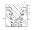
- the light emitting element 10 is provided inside a concave structure having the first member 41 as a side wall and the first electrode 21 as a bottom, and the concave structure is embedded by a second member 42. Accordingly, the second member 42 functions as a layer that propagates light emitted from the light emitting element 10 upward. Note that specific configurations of the light-emitting element 10 and the barrier layer 24 will be described later with reference to FIG.
- the first member 41 and second member 42 is formed of a material with refractive index n 1 of the first member 41, and the refractive index n 2 of the second member 42 satisfies n 2> n 1 relationship The Thereby, since the light propagated through the second member 42 is reflected on the surface of the first member 41 facing the second member 42, the surface of the first member 41 facing the second member 42 is It will function as a reflector (light reflecting portion).
- the concave structure in which the light emitting element 10 is provided has an inversely tapered shape that is inclined so that the opening area on the first electrode 21 side is reduced. Reflected upward at the interface with the two members 42. According to such a configuration, since the display device 1 can improve the light extraction efficiency from the light emitting element 10, it is possible to improve the luminance of the entire display device 1.
- the planarization layer 32 is provided on the second member 42 and planarizes unevenness caused by the structure provided below the second member 42.
- the planarizing layer 32 after forming and SiO x or SiN x, a surface is polished by CMP (Chemical Mechanical Polish), etc., it may be formed by flattening.
- the color filter layer 33 is provided on the planarizing layer 32. Specifically, the color filter layer 33 is provided so that the color filters of each color corresponding to each of the light emitting elements 10 are in a predetermined arrangement.
- the color filter layer 33 may be provided so that each of a red color filter, a green color filter, and a blue color filter having a predetermined area is distributed in a plane in a predetermined arrangement. That is, the display device 1 shown in FIG. 1 is a so-called on-chip color filter (OCCF) type display device in which the color filter layer 33 is provided on the first substrate 11 on which the light emitting element 10 is provided.
- the color filter layer 33 may include a black matrix that blocks light from the light emitting element 10 as necessary.
- the second substrate 34 is provided on the color filter layer 33 via a sealing resin such as an epoxy resin.
- the second substrate 34 may be made of, for example, quartz glass, but may be high strain point glass, soda glass (a mixture of Na 2 O, CaO, and SiO 2 ), borosilicate glass (Na 2 O, B 2 O 3).
- the second substrate 34 is preferably formed of a material having a high light transmittance that can suitably transmit the light from the light emitting element 10.
- the sealing resin it is preferable to use a material having high light transmittance with respect to the light emitted from the light emitting element 10.
- FIG. 2 is a schematic cross-sectional view showing an enlarged region where the light emitting element 10 of FIG. 1 is provided.
- the light emitting element 10 includes a first electrode 21, a first member 41 that forms a concave structure with the first electrode 21 as a bottom, and a concave formed by the first electrode 21 and the first member 41.
- the organic light emitting layer 23 is provided along the structure, and the second electrode 22 is provided on the organic light emitting layer 23.
- the barrier layer 24 is provided on the second electrode 22, and the concave structure formed by the first electrode 21 and the first member 41 is embedded by the second member 42 from above the barrier layer 24.
- the light emitting element 10 is formed in a concave structure having the first member 41 provided between the light emitting elements 10 as a side wall and the first electrode 21 as a bottom.
- the concave structure is embedded by the second member 42, and the refractive index n 2 of the second member 42 is larger than the refractive index n 1 of the first member 41.
- the surface of the first member 41 facing the second member 42 can function as a reflector that reflects the light propagated through the second member 42.
- the concave structure in which the light emitting element 10 is provided has a reverse taper shape in which the opening is widened toward the second substrate 34 side, the light emitted from the light emitting element 10 is the first member 41 and the second member 42. It is reflected upwards at the interface with. According to such a configuration, the light extraction efficiency from the light emitting element 10 can be improved.
- the first electrode 21 is provided for each light emitting element 10 and functions as an anode of the light emitting element 10.
- the first electrode 21 is provided at the bottom of the concave structure with the first member 41 as a side wall.
- the first electrode 21 is formed as a light reflecting electrode that reflects light emitted from the organic light emitting layer 23 with a material having high light reflectance. It is preferable.
- the first electrode 21 includes platinum (Pt), gold (Au), silver (Ag), chromium (Cr), tungsten (W), nickel (Ni), copper (Cu), iron (Fe), cobalt ( Co), tantalum (Ta), or other metal having a high work function may be used.
- the first electrode 21 is a laminated electrode obtained by laminating a transparent conductive material such as indium zinc oxide (IZO) or indium tin oxide (ITO) on a dielectric multilayer film or a thin film having high light reflectivity such as aluminum. May be formed.
- IZO indium zinc oxide
- ITO indium tin oxide
- the organic light emitting layer 23 includes an organic light emitting material, and is provided on the first electrode 21 and the first member 41 along the concave structure as a continuous film extending over the plurality of light emitting elements 10.
- the organic light emitting layer 23 can emit light when an electric field is applied between the first electrode 21 and the second electrode 22.
- the organic light emitting layer 23 may be formed in a multilayer structure in which a plurality of functional layers are stacked.
- the organic light emitting layer 23 may be formed in a multilayer structure in which a hole injection layer, a hole transport layer, a light emitting layer, an electron transport layer, and an electron injection layer are stacked in this order from the first electrode 21 side.
- the organic light emitting layer 23 may be formed in a so-called tandem structure in which a plurality of light emitting layers are connected via a charge generation layer or an intermediate electrode.
- the hole injection layer is a layer that includes a hole injection material and increases the efficiency of hole injection from the first electrode 21.
- the hole injection material known materials can be used. For example, triphenylamine-containing polyetherketone (TPAPEK), 4-isopropyl-4′-methyldiphenyliodonium tetrakis (pentafluorophenyl) borate (PPBI), N , N′-diphenyl-N, N′-bis- [4- (phenyl-m-tolyl-amino) -phenyl] -biphenyl-4,4′-diamine (DNTPD), copper phthalocyanine, 4,4 ′, 4 "-Tris (3-methylphenylphenylamino) triphenylamine (m-MTDATA), N, N'-di (1-naphthyl) -N, N'-diphenylbenzidine (NPB), 4,4 ', 4" -Tris (diphenylamin
- the hole transport layer is a layer that includes a hole transport material and enhances the efficiency of transporting holes from the first electrode 21.
- a hole transport material known materials can be used, for example, benzine, styrylamine, triphenylamine, porphyrin, triphenylene, azatriphenylene, tetracyanoquinodimethane, triazole, imidazole, oxadiazole, polyarylalkane. , Phenylenediamine, arylamine, oxazole, anthracene, fluorenone, hydrazone, stilbene, or derivatives thereof can be used.
- ⁇ -naphthylphenylphenylenediamine ⁇ -NPD
- porphyrin metal tetraphenylporphyrin
- metal naphthalocyanine hexacyanoazatriphenylene (HAT)
- 7,7,8,8- Tetracyanoquinodimethane TNQ
- 7,7,8,8-tetracyano-2,3,5,6-tetrafluoroquinodimethane F4-TCNQ
- tetracyano 4,4,4-tris (3-methyl Phenylphenylamino) triphenylamine, N, N, N ′, N′-tetrakis (p-tolyl) p-phenylenediamine, N, N, N ′, N′-tetraphenyl-4,4′-diaminobiphenyl, N-phenylcarbazole, 4-di-p-tolylaminostilbene, or the
- the light emitting layer includes a hole transport material that is a host material, an electron transport material, or at least one charge transport material of both charge transport materials, and a fluorescent or phosphorescent organic light emitting material that is a dopant material.
- a known charge transport material can be used as the host material.
- a styryl derivative, anthracene derivative, naphthacene derivative, carbazole derivative, aromatic amine derivative, phenanthroline derivative, triazole derivative, quinolinolato metal complex, or phenanthroline derivative can be used.
- fluorescent material a well-known fluorescent material and phosphorescent material can be used as a dopant material (organic luminescent material).
- Known fluorescent materials include, for example, dye materials such as styrylbenzene dyes, oxazole dyes, perylene dyes, coumarin dyes or acridine dyes, polyaromatics such as anthracene derivatives, naphthacene derivatives, pentacene derivatives, or chrysene derivatives.
- Hydrocarbon materials for example, ruthenium (Ru), rhodium (Rh), palladium (Pd), silver (Ag), rhenium (Re), osmium (Os), iridium (Ir), platinum (Pt) ), And an organometallic complex containing at least one metal selected from the group consisting of gold (Au).
- complexes such 3 such Ir (ppy) having a noble metal element of Ir such as the central metal, Ir (bt) complexes such as 2 ⁇ acac 3, complexes such as PtOEt 3 Can be used.
- the light emitting layer may emit light corresponding to each color of the display device instead of white.
- a red light-emitting layer that emits red light includes 4,4-bis (2,2-diphenylbinine) biphenyl (DPVBi) and 2,6-bis [(4′-methoxydiphenylamino) styryl] -1, It can be formed by mixing 30% by mass of 5-dicyanonaphthalene (BSN).
- the green light emitting layer which emits green light can be formed by mixing 5 mass% of coumarin 6 with DPVBi.
- the blue light-emitting layer emitting blue light is mixed with 2.5% by mass of 4,4′-bis [2- ⁇ 4- (N, N-diphenylamino) phenyl ⁇ vinyl] biphenyl (DPAVBi) in DPVBi. Can be formed.
- the electron transport layer is a layer that includes an electron transport material and increases the efficiency of electron injection from the second electrode 22.
- the electron transporting material known materials can be used. For example, tris (8-quinolinolato) aluminum (Alq 3 ) and a compound having a nitrogen-containing aromatic ring can be used. More specifically, as the electron transport material, the above-described tris (8-quinolinolato) aluminum (Alq 3 ), 2,9-dimethyl-4,7-diphenyl-1,10-phenanthroline (BCP), or bathophenanthroline (Bphen) ) Can be used.
- the electron transport layer may be composed of a plurality of layers. When the electron transport layer is formed of a plurality of layers, the electron transport layer may further include a layer doped with an alkali metal element or an alkaline earth metal element.
- the electron injection layer is a layer that increases the efficiency of electron injection from the second electrode 22.
- the electron injection layer may be formed of a known material, for example, lithium fluoride (LiF), sodium chloride (NaCl), cesium fluoride (CsF), lithium oxide (Li 2 O), or barium oxide (BaO). ) Or the like.
- the second electrode 22 functions as a cathode of the light emitting element and is provided on the organic light emitting layer 23 along the concave structure as a continuous film extending over the plurality of light emitting elements.
- the second electrode 22 is formed of a material having a high light transmittance as a transparent electrode that transmits light emitted from the organic light emitting layer 23. Is preferred.
- the second electrode 22 is made of aluminum (Al), silver (Ag), magnesium (Mg), calcium (Ca), sodium (Na), strontium (Sr), an alloy of an alkali metal and silver, or an alkaline earth metal. It may be formed of a metal or alloy having a low work function such as an alloy of silver and silver, an alloy of magnesium and calcium, or an alloy of aluminum and lithium.
- the second electrode 22 may be formed of a transparent conductive material such as indium zinc oxide (IZO) or indium tin oxide (ITO), and includes a layer made of the above-described material having a low work function, and indium zinc oxide. It may be formed as a laminated electrode with a layer made of a transparent conductive material such as (IZO) or indium tin oxide (ITO).
- the first member 41 is provided between the first electrodes 21 and separates the light emitting elements 10 from each other. Specifically, the first member 41 is formed around the first electrode 21 in a substantially trapezoidal shape (that is, a tapered shape) having an inclined portion. As a result, the first member 41 can form a concave structure with the first electrode 21 as a bottom and an opening area that increases toward the second substrate 34 (that is, an inversely tapered shape).
- the first member 41 is preferably formed of a material having a refractive index smaller than that of the second member 42.
- the first member 41 is made of, for example, an organic insulating material such as polyimide resin, acrylic resin, or novolac resin, or silicon oxide (SiO x ), silicon nitride (SiN x ), or silicon oxynitride (SiON). It may be formed of an inorganic insulating material or the like.
- the second member 42 is provided on the barrier layer 24 so as to embed the concave structure formed by the first member 41.
- the second member 42 is preferably formed of a material having a refractive index larger than that of the first member 41. Accordingly, the second member 42 can cause the surface of the first member 41 facing the second member 42 to function as a reflector that reflects at least a part of the light propagated through the second member 42.
- the second member 42 is made of, for example, a transparent organic insulating material such as polyimide resin, acrylic resin, or novolac resin, or silicon oxide (SiO x ), silicon nitride (SiN x ), or silicon oxynitride (SiON). It may be formed of a transparent inorganic insulating material or the like.
- the material having a high refractive index for forming the second member 42 is, for example, an organic resin containing a large amount of substituents having a high molecular refraction such as a sulfur-containing substituent, a phosphorus-containing substituent, or an aromatic ring in the molecular structure, or ITO.
- Inorganic oxides having a high refractive index such as IZO, TiO 2 , or Nb 2 O 5 can be exemplified.
- the second member 42 having a high refractive index can also be formed by allowing the second member 42 to contain a high refractive index inorganic filler such as TiO 2 or ZrO 2 .
- the barrier layer 24 is a layer provided on the second electrode 22 to prevent moisture and oxygen from entering the organic light emitting layer 23.
- the refractive index of the barrier layer 24 is controlled to be a value between the refractive index of the second electrode 22 and the refractive index of the second member 42.
- the barrier layer 24 can prevent a large variation in refractive index between the second electrode 22 and the second member 42 provided above and below the barrier layer 24.
- the barrier layer 24 can suppress unintentional reflection of the light emitted from the light emitting element 10.
- the barrier layer 24 having such a controlled refractive index can be formed of a laminate of a plurality of layers having different refractive indexes. This is because when the thickness of each layer of the laminate constituting the barrier layer 24 is extremely small with respect to the wavelength of incident light (for example, 1/50 or less of the wavelength of incident light), the incident light is This is because there is almost no interaction with each layer. In such a case, the barrier layer 24 behaves as if it is a single-layer film as a whole with respect to incident light. Note that the refractive index of the entire barrier layer 24 at this time is approximately a value obtained by averaging the refractive indexes of the respective layers of the laminated body constituting the barrier layer 24 by the film thickness ratio.
- the barrier layer 24 formed as a laminate of a plurality of layers having different refractive indexes can arbitrarily control the refractive index of the entire barrier layer 24 by the refractive index and film thickness of each layer constituting the laminate. Is possible. According to this, the barrier layer 24 suppresses light reflection by controlling the refractive index in accordance with the refractive index of the second electrode 22 provided above and below and the refractive index of the second member 42. It is possible to do so. Therefore, the barrier layer 24 according to the present embodiment can suppress the light emitted from the light emitting element 10 from being reflected at an unintended interface between layers, thereby improving the light extraction efficiency of the light emitting element 10. it can.
- the barrier layer 24 can be formed as a laminated body of a plurality of layers, thereby improving the barrier property against moisture and oxygen.
- the reason for this is not clear, but by laminating different layers, the crystallization of each layer is suppressed, so the formation of crystal grain boundaries or crystal defects that serve as paths for gas molecules, etc. Is considered to be suppressed.
- the barrier layer 24 may be formed as a laminate of two types of layers having different refractive indexes, or may be formed as a laminate of three or more types of layers having different refractive indexes.
- FIG. 3 is a schematic cross-sectional view showing a more specific configuration of the barrier layer 24.
- the barrier layer 24 can be formed by repeatedly laminating two types of layers having different refractive indexes.
- the barrier layer 24 includes protective layers 241A, 241B, 241C, and 241D (hereinafter collectively referred to as protective layers 241) made of a material having a high barrier property against moisture and oxygen, and a material having a high refractive index. It may be formed as a laminate in which the refractive index adjustment layers 242A, 242B, 242C, and 242D (hereinafter collectively referred to as a refractive index adjustment layer 242) are alternately laminated.
- the present embodiment is not limited to this.
- the number of repetitions of stacking the barrier layer 24 may be at least once.
- the upper limit of the repetition number of lamination is not particularly limited.
- the protective layer 241 and the refractive index adjustment layer 242 are formed of an inorganic material containing different elements, and the difference between the refractive index of the protective layer 241 and the refractive index of the refractive index adjustment layer 242 is 0.1. It may be the above.
- the barrier layer 24 can easily optimize the barrier property against moisture and oxygen and the refractive index in the entire barrier layer 24. become.
- the material having a high barrier property against moisture and oxygen for forming the protective layer 241 include Al 2 O 3 , SiN x , SiO 2 , SiON, SiC, and SiCO.
- Specific examples of the material having a high refractive index for forming the refractive index adjusting layer 242 include metal oxides, such as TiO 2 , ZrO 2 , ZnO, Ta 2 O 5 , HfO 2. , And Nb 2 O 5 . By using such a material, the barrier layer 24 can control the refractive index to an arbitrary value by the refractive index adjustment layer 242 while ensuring the barrier property against moisture and oxygen by the protective layer 241.
- either the film thickness of the protective layer 241 or the film thickness of the refractive index adjusting layer 242 is preferably 10 nm or less.
- the film thickness of the protective layer 241 or the refractive index adjustment layer 242 depends on the wavelength of the incident light. In contrast to (approximately 360 nm to 830 nm), it is preferably small enough to be ignored. Therefore, either the film thickness of the protective layer 241 or the film thickness of the refractive index adjustment layer 242 is preferably 10 nm or less.
- the ratio between the thickness of the protective layer 241 and the thickness of the refractive index adjustment layer 242 in the repeating unit may be any ratio as long as the thickness of each layer is in the above-described range. Further, the ratio between the thickness of the protective layer 241 and the thickness of the refractive index adjustment layer 242 in the repeating unit may be different for each repeating unit.
- the total film thickness of the repeating units composed of the protective layer 241 and the refractive index adjusting layer 242 is preferably 24 nm or less.
- the barrier layer 24 is formed as a laminated body in which repeating units composed of a protective layer 241 and a refractive index adjusting layer 242 are further laminated. Therefore, the total film thickness of the repeating units composed of the protective layer 241 and the refractive index adjusting layer 242 is also preferably small with respect to the wavelength of incident light (approximately 360 nm to 830 nm). From the results shown in FIG. It is preferable that it is 24 nm or less.
- the barrier layer 24 behaves as a multi-layer stack with respect to the incident light, so that the light This is not preferable because of the increase in reflection.
- the barrier layer 24 is made of Al 2 O 3 with a film thickness of 7 nm to 15 nm.
- a protective layer 241 formed below may be constituted by a laminate of alternately laminated refractive index adjusting layer 242 formed in a thickness of 0.5nm or more 5nm below in TiO 2.
- FIG. 4 is a schematic cross-sectional view illustrating the laminated structure of the barrier layer 24 according to the test example.
- the barrier layer 24 is a laminate in which protective layers 241A and 241B made of Al 2 O 3 and refractive index adjustment layers 242A and 242B made of TiO 2 are alternately and repeatedly laminated. Consists of the body. Note that ALD (Atomic Layer Deposition) was used to form the protective layers 241A and 241B and the refractive index adjustment layers 242A and 242B.
- ALD Atomic Layer Deposition
- the protective layer 241A, the thickness of 241B as t 1, the refractive index adjustment layer 242A, the thickness of 242B and t 2 the thickness of the repeating units consisting of the protective layer 241A and the refractive index adjusting layer 242A (i.e., t 1 + t 2 ) was t unit, and the film thickness of the entire barrier layer 24 was t total .
- the film thickness t unit of the repeating unit is set to 10 nm
- the film thickness t total of the entire barrier layer 24 is set to 20 nm
- the ratio of t 1 and t 2 is changed to control the refractive index of the entire barrier layer 24. Confirmed that it was possible.
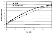
- FIG. FIG. 5 is a graph showing the effective refractive index of the barrier layer 24 when the ratio of the refractive index adjustment layer 242 made of TiO 2 is changed (note that the wavelength of incident light is 550 nm).
- the effective refractive index of the barrier layer 24 was calculated using spectroscopic ellipsometry.
- Spectral ellipsometry is a measurement method that can calculate the optical constant of a sample from the change in the polarization of reflected light with respect to the polarization of incident light irradiated on the sample by giving a film configuration model of the sample.
- the film configuration model of the barrier layer 24 by using the film configuration model when it is assumed that the barrier layer 24 is a single layer film without using the actual film configuration of the stacked body, the barrier layer 24 is used.
- the overall refractive index was calculated as the effective refractive index.
- the least square error indicating the fitting error between the measured value and the value calculated from the film configuration model of the given sample is also calculated.
- the least square error is large, it indicates that the actual film configuration of the sample is not consistent with the film configuration model of the given sample. That is, when the least square error of the barrier layer 24 composed of the laminate is large, an interaction occurs between each layer of the laminate constituting the barrier layer 24 and the incident light. It can be seen that the barrier layer 24 does not behave as a single layer film.
- the case where the ratio of the refractive index adjustment layer 242 made of TiO 2 is changed by the film thickness is shown by a square point plot, and the ratio of the refractive index adjustment layer 242 made of TiO 2 is expressed by the number of film formation cycles by ALD.
- the case of changing is shown by a plot of diamond points. Since ALD can form atoms one by one, the number of film formation cycles by ALD is considered to correspond to the number of crystal lattices of the formed layer. In the results shown in FIG. 5, it was confirmed that the least square error of spectroscopic ellipsometry was small, and the barrier layer 24 behaved as a single layer film with respect to incident light.
- the refractive index of the entire barrier layer 24 increases as the proportion of TiO 2 having a higher refractive index than Al 2 O 3 increases.
- the barrier layer 24 is composed of a single layer film of Al 2 O 3.
- the barrier layer 24 is a single layer of TiO 2 . This is a case of being composed of a layer film. Therefore, it can be seen that the refractive index of the entire barrier layer 24 is an intermediate value of the refractive index of each layer to be laminated.
- the ratio of TiO 2 calculated from the film formation cycle of ALD is higher than the ratio of TiO 2 calculated from the film thickness of the refractive index adjustment layer 242, the linearity with respect to the entire refractive index of the barrier layer 24 is higher. It can be seen that for ultrathin films, the number of crystal lattices is more important for controlling the refractive index than the film thickness.
- the barrier layer 24 can be regarded as a single layer film.
- the film thickness of each layer was examined. The result is shown in FIG. FIG. 6 is a graph showing the least square error of the spectroscopic ellipsometer when the film thickness t unit of the repeating unit is changed.
- the barrier layer 24 is a single layer film of Al 2 O 3 .
- the film thickness t unit of the repeating unit is 24 nm
- the least square error by spectroscopic ellipsometry increases rapidly.
- the minimum square error is almost the same value as the case where the barrier layer 24 is a single layer film until the film thickness t unit of the repeating unit is about 12 nm
- the barrier layer 24 configured as a multilayered structure is formed. It can be seen that it can be regarded as a single layer film. Therefore, it can be seen that the total thickness of the repeating units of the barrier layer 24 is preferably 24 nm or less.
- the light emitting device 10 by forming a barrier layer with a stack of a plurality of layers having different refractive indexes, the light of unintended light inside the light emitting device 10 can be obtained. It is possible to suppress reflection. According to this, since the light which goes upwards from the light emitting element 10 can be increased, the light extraction efficiency from the light emitting element 10 can be improved.
- FIGS. 7 to 11 are cross-sectional views schematically showing each step of the method for manufacturing the light emitting element 10 according to this embodiment.
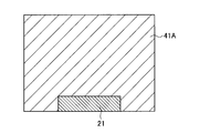
- the first member layer 41 ⁇ / b> A is formed on the first electrode 21.
- the first electrode 21 that is electrically connected to various circuits including the transistor TFT is formed by sputtering or the like.
- the first electrode 21 may be formed of an aluminum copper alloy (AlCu), or may be formed of a multilayer film in which an aluminum copper alloy (AlCu) and indium tin oxide are sequentially stacked from the bottom.
- the first member layer 41A is formed on the first electrode 21 by using CVD (Chemical Vapor Deposition) or the like.
- the first member layer 41A is a layer that forms the first member 41 by being patterned by subsequent etching, and may be formed of, for example, silicon oxide (SiO x ) or the like.
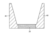
- the first member layer 41A is patterned using etching or the like so that the first electrode 21 is exposed.
- a concave structure is formed with the first electrode 21 as the bottom and the first member 41 as the side wall.
- the concave structure may be formed in a reverse tapered shape in which the opening area of the surface on which the first electrode 21 is provided is smaller than the opening area of the opposing surface by controlling the etching conditions. preferable.
- the organic light emitting layer 23 is formed along the concave structure on the first electrode 21 and the first member 41, and the second along the concave structure is formed on the organic light emitting layer 23. Electrode 22 is formed.
- a hole injection layer, a hole transport layer, a light emitting layer, and an electron transport layer are formed on the first electrode 21 and the first member 41 from the first electrode 21 side using a vacuum deposition method.
- the organic light emitting layer 23 is formed by sequentially forming the electron injection layer and the electron injection layer. Note that the materials described above can be used as the material of each layer.
- the second electrode 22 is formed on the organic light emitting layer 23 using sputtering or the like.
- the second electrode 22 may be formed of a transparent conductive material such as indium zinc oxide or indium tin oxide.
- a barrier layer 24 is formed on the second electrode 22.
- the barrier layer 24 is formed as a stacked body of a plurality of layers having different refractive indexes by using CVD, sputtering, ALD (Atomic Layer Deposition), or ion plating.
- the barrier layer 24 may be formed as a laminate in which Al 2 O 3 and TiO 2 are alternately and repeatedly laminated in nanometer order using ALD.
- the barrier layer 24 is formed so that the refractive index value of the entire barrier layer 24 is an intermediate value between the refractive index of the second electrode 22 and the refractive index of the second member 42.
- the second member 42 is formed on the barrier layer 24 so as to embed the concave structure formed by the first member 41.
- the second member 42 can be formed so as to embed a concave structure on the barrier layer 24 by using a spin coating method or the like. Alternatively, after the second member 42 is formed over the entire surface of the barrier layer 24, the second member 42 formed outside the inside of the concave structure is removed by using CMP or etch back, whereby the first member 42 is removed.
- Two members 42 can be formed.
- the second member 42 may be formed of an acrylic resin in which a filler made of TiO 2 or ZrO 2 is dispersedly contained.
- the display device 1 is formed.
- the light emitting element 10 and the display device 1 according to the present embodiment can be manufactured.
- said manufacturing method is an example to the last, and the manufacturing method of the light emitting element 10 which concerns on this embodiment, and the display apparatus 1 is not limited above.
- FIGS. 12 to 15 are external views illustrating an example of a display device or an electronic apparatus to which the light emitting element 10 according to an embodiment of the present disclosure can be applied.
- the light emitting element 10 according to the present embodiment can be applied to a pixel element of a display unit included in an electronic device such as a smartphone.
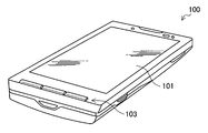
- the smartphone 100 includes a display unit 101 that displays various types of information, and an operation unit 103 that includes buttons that accept operation inputs from the user.
- the display unit 101 may include the light emitting element 10 according to the present embodiment, and may be configured by the display device 1 according to the present embodiment.
- the light emitting element 10 according to the present embodiment can be applied to a pixel element of a display unit of an electronic device such as a digital camera.
- the digital camera 110 includes a main body (camera body) 111, an interchangeable lens unit 113, a grip portion 115 that is gripped by a user during shooting, A monitor unit 117 that displays information and an EVF (Electronic View Finder) 119 that displays a through image observed by the user at the time of shooting.
- 13 shows an external view of the digital camera 110 viewed from the front (that is, the subject side)
- FIG. 14 shows an external view of the digital camera 110 viewed from the back (that is, the photographer side).
- the monitor unit 117 and the EVF 119 may include the light emitting element 10 according to the present embodiment, and may be configured by the display device 1 according to the present embodiment.
- the light emitting element 10 according to the present embodiment can be applied to a display unit of an electronic device such as an HMD (Head Mounted Display).
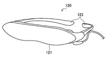
- the HMD 120 includes a glasses-type display unit 121 that displays various types of information, and an ear hook unit 123 that is hooked on the user's ear when worn.
- the display unit 121 may include the light emitting element 10 according to the present embodiment, and may be configured by the display device 1 according to the present embodiment.
- the light emitting element 10 according to the present embodiment can be applied to a display unit of an electronic device in any field that performs display based on an image signal input from the outside or an image signal generated inside.
- Examples of such an electronic device include a television device, an electronic book, a PDA (Personal Digital Assistant), a notebook personal computer, a video camera, or a game device.
- the present disclosure is not limited to such an example.
- the display device targeted by the present disclosure may be any display device as long as it can realize color display, such as a liquid crystal display, a plasma display, and electronic paper.
- the barrier layer is formed as a laminate and the refractive index of the barrier layer is controlled so that unintended light reflection does not occur. It is possible to obtain the effect of improving the light extraction efficiency.
- the light emitting element is a portion that emits light toward the outside in each pixel of the display device.
- the light emitting element corresponds to an organic light emitting layer (that is, an organic EL element) sandwiched between the lower electrode and the upper electrode.
- the light emitting element corresponds to one pixel of a liquid crystal panel provided with a backlight.
- the light emitting element corresponds to one discharge cell in the plasma display panel.
- a first electrode A first member provided on both sides of the first electrode and forming a concave structure with the first electrode as a bottom;
- An organic light emitting layer comprising an organic light emitting material and provided on the first electrode and the first member along the concave structure;
- a second electrode provided on the organic light emitting layer;
- a second member having a refractive index higher than that of the first member and provided on the second electrode so as to embed the concave structure;
- the said laminated body is a light emitting element as described in said (1) which is a laminated body which laminated
- the light emitting element according to (2) wherein the film thickness of at least one of the two types of layers is 10 nm or less.
- the said laminated body is a light emitting element as described in said (1) which is a laminated body which laminated
- the light emitting device according to (8), wherein the metal oxide is any one of TiO 2 , ZrO 2 , ZnO, Ta 2 O 5 , HfO 2 , or Nb 2 O 5 .
- a second member provided on the second electrode, and the laminate is formed as a laminate of a plurality of layers having different refractive indexes between the second electrode and the second member.
- a display unit in which a plurality of light-emitting elements provided with a barrier layer having a refractive index as a whole between the refractive index of the second electrode and the refractive index of the second member are arranged on a plane;
- a display control unit for controlling the display unit;
- a display device comprising: (11) A first member, a first member provided on both sides of the first electrode, forming a concave structure with the first electrode as a bottom, an organic light emitting material, and the first electrode and the first electrode along the concave structure; An organic light emitting layer provided on the first member, a second electrode provided on the organic light emitting layer, and a refractive index higher than a refractive index of the first member so as to embed the concave structure
- a second member provided on the second electrode, and the laminate is formed as a laminate of a plurality of layers having different refractive indexes between the second electrode and the second member.
- a display unit in which a plurality of light-emitting elements provided with a barrier layer having a refractive index as a whole between the refractive index of the second electrode and the refractive index of the second member are arranged on a plane;
- a control unit for controlling the display unit;
- An electronic device for controlling the display unit;
Landscapes
- Engineering & Computer Science (AREA)
- Chemical & Material Sciences (AREA)
- Inorganic Chemistry (AREA)
- Physics & Mathematics (AREA)
- Microelectronics & Electronic Packaging (AREA)
- Optics & Photonics (AREA)
- General Physics & Mathematics (AREA)
- Theoretical Computer Science (AREA)
- Electroluminescent Light Sources (AREA)
- Devices For Indicating Variable Information By Combining Individual Elements (AREA)
Abstract
【課題】光取出し効率が向上した発光素子、表示装置、および電子機器を提供する。 【解決手段】第1電極と、前記第1電極の両側に設けられ、前記第1電極を底部とする凹構造を形成する第1部材と、有機発光材料を含み、前記凹構造に沿って前記第1電極および前記第1部材の上に設けられる有機発光層と、前記有機発光層の上に設けられる第2電極と、前記第1部材の屈折率よりも高い屈折率を有し、前記凹構造を埋め込むように前記第2電極の上に設けられる第2部材と、を備え、前記第2電極および前記第2部材の間には、異なる屈折率を有する複数の層の積層体として形成され、前記積層体の全体での屈折率が前記第2電極の屈折率と、前記第2部材の屈折率との間の値であるバリア層が設けられる、発光素子。
Description
本開示は、発光素子、表示装置、および電子機器に関する。
近年、有機エレクトロルミネッセンス素子(いわゆる、有機EL素子)を発光素子として用いる照明装置または表示装置が普及しつつある。このような照明装置または表示装置に用いられる発光素子では、輝度を向上させるために、発光源からより効率的に光を取り出すことが求められている。
例えば、下記の特許文献1には、有機EL素子を凹構造の底部に形成し、屈折率差によって凹構造の内部側面をリフレクタとして機能させることで、有機EL素子からの光取出し効率を向上させる表示装置が開示されている。
しかし、特許文献1に開示された表示装置では、発光素子を構成する層ごとに屈折率が異なるため、発光素子から発せられた光は、様々な層の界面で複数回反射する可能性があった。したがって、特許文献1に開示された表示装置では、意図しない反射によって、発光素子からの光取出し効率が低下する可能性があった。
そこで、本開示では、光取出し効率をより向上させることが可能な、新規かつ改良された発光素子、表示装置、および電子機器を提案する。
本開示によれば、第1電極と、前記第1電極の両側に設けられ、前記第1電極を底部とする凹構造を形成する第1部材と、有機発光材料を含み、前記凹構造に沿って前記第1電極および前記第1部材の上に設けられる有機発光層と、前記有機発光層の上に設けられる第2電極と、前記第1部材の屈折率よりも高い屈折率を有し、前記凹構造を埋め込むように前記第2電極の上に設けられる第2部材と、を備え、前記第2電極および前記第2部材の間には、異なる屈折率を有する複数の層の積層体として形成され、前記積層体の全体での屈折率が前記第2電極の屈折率と、前記第2部材の屈折率との間の値であるバリア層が設けられる、発光素子が提供される。
また、本開示によれば、第1電極と、前記第1電極の両側に設けられ、前記第1電極を底部とする凹構造を形成する第1部材と、有機発光材料を含み、前記凹構造に沿って前記第1電極および前記第1部材の上に設けられる有機発光層と、前記有機発光層の上に設けられる第2電極と、前記第1部材の屈折率よりも高い屈折率を有し、前記凹構造を埋め込むように前記第2電極の上に設けられる第2部材と、を備え、前記第2電極および前記第2部材の間には、異なる屈折率を有する複数の層の積層体として形成され、前記積層体の全体での屈折率が前記第2電極の屈折率と、前記第2部材の屈折率との間の値であるバリア層が設けられる発光素子を平面上に複数配列した表示部と、前記表示部を制御する表示制御部と、を備える、表示装置が提供される。
さらに、本開示によれば、第1電極と、前記第1電極の両側に設けられ、前記第1電極を底部とする凹構造を形成する第1部材と、有機発光材料を含み、前記凹構造に沿って前記第1電極および前記第1部材の上に設けられる有機発光層と、前記有機発光層の上に設けられる第2電極と、前記第1部材の屈折率よりも高い屈折率を有し、前記凹構造を埋め込むように前記第2電極の上に設けられる第2部材と、を備え、前記第2電極および前記第2部材の間には、異なる屈折率を有する複数の層の積層体として形成され、前記積層体の全体での屈折率が前記第2電極の屈折率と、前記第2部材の屈折率との間の値であるバリア層が設けられる発光素子を平面上に複数配列した表示部と、前記表示部を制御する制御部と、を備える、電子機器が提供される。
本開示によれば、意図しない層の界面で光の反射が生じることを抑制することができるため、発光素子からの光取出し効率を向上させることが可能である。
以上説明したように本開示によれば、光取出し効率が向上した発光素子、表示装置、および電子機器を提供することが可能である。
なお、上記の効果は必ずしも限定的なものではなく、上記の効果とともに、または上記の効果に代えて、本明細書に示されたいずれかの効果、または本明細書から把握され得る他の効果が奏されてもよい。
以下に添付図面を参照しながら、本開示の好適な実施の形態について詳細に説明する。なお、本明細書及び図面において、実質的に同一の機能構成を有する構成要素については、同一の符号を付することにより重複説明を省略する。
なお、説明は以下の順序で行うものとする。
1.表示装置の構成
2.発光素子の構成
3.バリア層の構成
4.製造方法
5.適用例
1.表示装置の構成
2.発光素子の構成
3.バリア層の構成
4.製造方法
5.適用例
<1.表示装置の構成>
まず、図1を参照して、本開示の一実施形態に係る表示装置の構成について説明する。図1は、本開示の一実施形態に係る表示装置を積層方向に切断した断面を模式的に示す断面図である。
まず、図1を参照して、本開示の一実施形態に係る表示装置の構成について説明する。図1は、本開示の一実施形態に係る表示装置を積層方向に切断した断面を模式的に示す断面図である。
図1に示すように、表示装置1は、第1基板11の上に設けられた複数のトランジスタTFTと、トランジスタTFTの各々と電気的に接続された複数の発光素子10と、複数の発光素子10の上に平坦化層32を介して設けられたカラーフィルタ層33と、カラーフィルタ層33の上に設けられた第2基板34とを備える。図1で示す表示装置1は、第2基板34を介して、発光素子10から光を取り出す上面発光型の表示装置であるが、第1基板11を介して光を取り出す下面発光型の表示装置であってもよい。
なお、以下の説明では、表示装置1における各層の積層方向を上下方向と表現する。また、第1基板11が配置される方向を下方向と表現し、第2基板34が配置される方向を上方向と表現する。
第1基板11は、例えば、単結晶、多結晶、またはアモルファスのシリコン(Si)基板にて構成される。シリコン等の半導体からなる基板は、微細加工が容易であるため、トランジスタTFT、および発光素子10をより微細に形成することが容易である。
トランジスタTFTは、発光素子10の各々に対応して設けられ、発光素子10の各々の駆動を制御する。具体的には、トランジスタTFTによって任意の発光素子10が選択的に駆動されることで、駆動された発光素子10から光が射出され、所望の画像または文字等が表示装置1に表示される。
例えば、トランジスタTFTは、薄膜トランジスタ(Thin Film Transistor:TFT)であってもよい。このような場合、トランジスタTFTは、第1基板11の上に設けられるゲート電極12と、第1基板11およびゲート電極12の上に設けられるゲート絶縁膜13と、ゲート絶縁膜13の上に設けられる半導体層15とから構成されてもよい。この構成によれば、半導体層15は、ゲート電極12の直上に位置する領域がチャネル領域15Aとして機能し、チャネル領域15Aを挟むように位置する領域がソース/ドレイン領域15Bとして機能する。なお、図1では、ボトムゲート型のトランジスタTFTを示したが、トランジスタTFTは、トップゲート型であってもよい。これらの層を構成する材料については、公知の材料を用いることが可能である。
また、半導体層15の上層には、下層絶縁層16A、および上層絶縁層16Bが設けられる。下層絶縁層16Aには、ソース/ドレイン領域15Bの直上に相当する領域に開口が設けられ、該開口を埋め込むようにコンタクト17Aが設けられる。さらに、コンタクト17Aの上には、配線17が設けられ、配線17およびトランジスタTFTを埋め込むように、上層絶縁層16Bが設けられる。
上層絶縁層16Bには、配線17が設けられた領域に開口が設けられ、該開口を介して配線17と電気的に接続するように接続配線18が設けられる。また、接続配線18は、上層絶縁層16Bの上にも延伸して設けられ、発光素子10の第1電極21として機能する。これにより、発光素子10では、第1電極21は、接続配線18を介して配線17と電気的に接続することで、トランジスタTFTのソース/ドレイン領域15Bと電気的に接続する。
なお、コンタクト17A、配線17、および接続配線18等は、銅(Cu)、アルミニウム(Al)、金(Au)、白金(Pt)、チタン(Ti)、クロム(Cr)、もしくはタングステン(W)などの金属または合金で形成することができる。また、下層絶縁層16A、および上層絶縁層16Bは、酸化シリコン(SiOx)系材料(例えば、SiO2、BPSG、PSG、BSG、AsSG、PbSG、SiON、SOG、低融点ガラス、又はガラスペースト等)、窒化シリコン(SiNx)系材料、酸窒化シリコン(SiON)系材料、または絶縁性樹脂(例えば、ポリイミド樹脂、ノボラック系樹脂、アクリル系樹脂、ポリベンゾオキサゾール等)を単独で、または複数種を組み合わせることで形成することができる。なお、これらの構成は、上述した材料以外にも公知の材料であれば適宜用いて形成することができる。
発光素子10は、トランジスタTFTなどを埋め込んだ上層絶縁層16Bの上に設けられ、例えば、第1電極21と、第1電極21の上に設けられた有機発光層23と、有機発光層23の上に設けられた第2電極22とから構成される。発光素子10は、第1電極21および第2電極22に挟持された有機発光層23に電界が印加されることで光を出射する。また、第2電極22の上には、発光素子10(特に、有機発光層23)を大気中の酸素および水分から保護するために、バリア層24が設けられる。
発光素子10は、第1部材41を側壁とし、第1電極21を底部とする凹構造の内部に設けられ、該凹構造は、第2部材42によって埋め込まれる。これにより、第2部材42は、発光素子10からの出射される光を上方に向かって伝播する層として機能する。なお、発光素子10、およびバリア層24の具体的な構成については、図2を参照して、後述する。
ここで、第1部材41および第2部材42は、第1部材41の屈折率n1と、第2部材42の屈折率n2とがn2>n1の関係を満たす材料にて形成される。これにより、第2部材42と対向する第1部材41の表面では、第2部材42を伝播した光が反射されるようになるため、第2部材42と対向する第1部材41の表面は、リフレクタ(光反射部)として機能することになる。
また、発光素子10が設けられる凹構造は、第1電極21側の開口面積が減少するように傾斜した逆テーパ形状を有するため、発光素子10から出射された光は、第1部材41と第2部材42との界面にて、上方に向かって反射されることとなる。このような構成によれば、表示装置1は、発光素子10からの光取り出し効率を向上させることができるため、表示装置1全体での輝度を向上させることができる。
平坦化層32は、第2部材42の上に設けられ、第2部材42より下に設けられた構造によって生じた凹凸を平坦化する。例えば、平坦化層32は、SiOxまたはSiNxなどを成膜した後に、表面をCMP(Chemical Mechanical Polish)等によって研磨し、平坦化することによって形成されてもよい。
カラーフィルタ層33は、平坦化層32の上に設けられる。具体的には、カラーフィルタ層33は、発光素子10の各々に対応する各色のカラーフィルタが所定の配置となるように設けられる。例えば、カラーフィルタ層33は、所定の面積を有する赤色カラーフィルタ、緑色カラーフィルタ、および青色カラーフィルタの各々が所定の配置で面内に分布するように設けられてもよい。すなわち、図1で示す表示装置1は、発光素子10が設けられた第1基板11の上にカラーフィルタ層33が設けられる、いわゆるオンチップカラーフィルタ(OCCF)方式の表示装置である。また、カラーフィルタ層33は、必要に応じて、発光素子10からの光を遮蔽するブラックマトリクスを含んでもよい。
第2基板34は、カラーフィルタ層33の上に、エポキシ樹脂等の封止樹脂を介して設けられる。第2基板34は、例えば、石英ガラスで構成されてもよいが、高歪点ガラス、ソーダガラス(Na2O、CaOおよびSiO2の混合物)、ホウケイ酸ガラス(Na2O、B2O3およびSiO2の混合物)、フォルステライト(Mg2SiO4)、鉛ガラス(Na2O、PbOおよびSiO2の混合物)、石英、または有機樹脂(例えば、ポリメチルメタクリレート(PMMA)、ポリビニルアルコール(PVA)、ポリビニルフェノール(PVP)、ポリエーテルスルホン(PES)、ポリイミド、ポリカーボネート、またはポリエチレンテレフタレート(PET)等)にて形成されてもよく、他の公知の材料で形成されてもよい。ただし、第2基板34は、発光素子10からの光を好適に透過させることが可能な、光透過率の高い材料によって形成されることが好ましい。また、封止樹脂についても、発光素子10からの出射光に対する光透過性が高い材料を用いることが好ましい。
<2.発光素子の構成>
次に、図2を参照して、本実施形態に係る表示装置1に備えられる発光素子10についてより詳細に説明する。図2は、図1の発光素子10が設けられた領域を拡大して示した模式的な断面図である。
次に、図2を参照して、本実施形態に係る表示装置1に備えられる発光素子10についてより詳細に説明する。図2は、図1の発光素子10が設けられた領域を拡大して示した模式的な断面図である。
図2に示すように、発光素子10は、第1電極21と、第1電極21を底部とする凹構造を形成する第1部材41と、第1電極21および第1部材41が形成する凹構造に沿って設けられた有機発光層23と、有機発光層23の上に設けられた第2電極22と、から構成される。また、第2電極22の上にはバリア層24が設けられ、第1電極21および第1部材41が形成する凹構造は、バリア層24の上から第2部材42によって埋め込まれている。
上述したように、発光素子10は、発光素子10の各々の間に設けられた第1部材41を側壁とし、第1電極21を底部とする凹構造の内部に形成される。また、該凹構造は、第2部材42によって埋め込まれ、第2部材42の屈折率n2は、第1部材41の屈折率n1よりも大きい。このため、第2部材42と対向する第1部材41の表面は、第2部材42を伝播した光を反射するリフレクタとして機能させることができる。
さらに、発光素子10が設けられる凹構造は、第2基板34側に向かって開口が広がった逆テーパ形状を有するため、発光素子10から出射された光は、第1部材41と第2部材42との界面にて、上方に向かって反射されることとなる。このような構成によれば、発光素子10からの光取り出し効率を向上させることができる。
第1電極21は、発光素子10ごとに設けられ、発光素子10のアノードとして機能する。また、第1電極21は、第1部材41を側壁とする凹構造の底部に設けられる。上述したように表示装置1は、上面発光型であるため、第1電極21は、光反射率が高い材料にて、有機発光層23から出射される光を反射する光反射電極として形成されることが好ましい。
例えば、第1電極21は、白金(Pt)、金(Au)、銀(Ag)、クロム(Cr)、タングステン(W)、ニッケル(Ni)、銅(Cu)、鉄(Fe)、コバルト(Co)、もしくはタンタル(Ta)などの仕事関数が高い金属の単体または合金などで形成されてもよい。また、第1電極21は、誘電体多層膜またはアルミニウムなどの光反射性の高い薄膜の上に、酸化インジウム亜鉛(IZO)または酸化インジウムスズ(ITO)などの透明導電性材料を積層した積層電極として形成されてもよい。
有機発光層23は、有機発光材料を含み、複数の発光素子10に亘る連続膜として、凹構造に沿って第1電極21および第1部材41の上に設けられる。有機発光層23は、第1電極21と、第2電極22との間で電界が印加されることによって発光することができる。
具体的には、有機発光層23に電界が印加された場合、有機発光層23では、第1電極21から正孔が注入され、第2電極22から電子が注入される。注入された正孔および電子は、有機発光層23中で再結合することで励起子を形成し、形成された励起子のエネルギーが有機発光材料を励起させることで、有機発光材料から蛍光またはりん光が発生する。
ここで、有機発光層23は、複数の機能層を積層した多層構造にて形成されてもよい。例えば、有機発光層23は、第1電極21側から順に、正孔注入層、正孔輸送層、発光層、電子輸送層、および電子注入層を積層した多層構造で形成されてもよい。また、有機発光層23は、複数の発光層を電荷発生層または中間電極を介して接続した、いわゆるタンデム型構造で形成されてもよい。
正孔注入層は、正孔注入材料を含み、第1電極21からの正孔の注入効率を高める層である。正孔注入材料は、公知のものを用いることができ、例えば、トリフェニルアミン含有ポリエーテルケトン(TPAPEK)、4-イソプロピル-4’-メチルジフェニルヨードニウムテトラキス(ペンタフルオロフェニル)ボラート(PPBI)、N,N’-ジフェニル-N,N’-ビス-[4-(フェニル-m-トリル-アミノ)-フェニル]-ビフェニル-4,4’-ジアミン(DNTPD)、銅フタロシアニン、4,4’,4”-トリス(3-メチルフェニルフェニルアミノ)トリフェニルアミン(m-MTDATA)、N,N’-ジ(1-ナフチル)-N,N’-ジフェニルベンジジン(NPB)、4,4’,4”-トリス(ジフェニルアミノ)トリフェニルアミン(TDATA)、4,4’,4”-トリス(N,N-2-ナフチルフェニルアミノ)トリフェニルアミン(2-TNATA)等を挙げることができる。
正孔輸送層は、正孔輸送材料を含み、第1電極21からの正孔の輸送効率を高める層である。正孔輸送材料は、公知のものを用いることができ、例えば、ベンジン、スチリルアミン、トリフェニルアミン、ポルフィリン、トリフェニレン、アザトリフェニレン、テトラシアノキノジメタン、トリアゾール、イミダゾール、オキサジアゾール、ポリアリールアルカン、フェニレンジアミン、アリールアミン、オキザゾール、アントラセン、フルオレノン、ヒドラゾン、もしくはスチルベン、またはこれらの誘導体などを用いることができる。
より具体的には、正孔輸送材料として、α-ナフチルフェニルフェニレンジアミン(α-NPD)、ポルフィリン、金属テトラフェニルポルフィリン、金属ナフタロシアニン、ヘキサシアノアザトリフェニレン(HAT)、7,7,8,8-テトラシアノキノジメタン(TCNQ)、7,7,8,8-テトラシアノ-2,3,5,6-テトラフルオロキノジメタン(F4-TCNQ)、テトラシアノ4,4,4-トリス(3-メチルフェニルフェニルアミノ)トリフェニルアミン、N,N,N’,N’-テトラキス(p-トリル)p-フェニレンジアミン、N,N,N’,N’-テトラフェニル-4,4’-ジアミノビフェニル、N-フェニルカルバゾール、または4-ジ-p-トリルアミノスチルベン等を用いることができる。
発光層は、ホスト材料である正孔輸送材料、電子輸送材料、または両電荷輸送材料の少なくとも1つ以上の電荷輸送材料と、ドーパント材料である蛍光性またはりん光性の有機発光材料とを含み、電気エネルギーを光エネルギーに変換する層である。
ホスト材料としては、公知の電荷輸送材料を用いることができ、例えば、スチリル誘導体、アントラセン誘導体、ナフタセン誘導体、カルバゾール誘導体、芳香族アミン誘導体、フェナントロリン誘導体、トリアゾール誘導体、キノリノラト系金属錯体、またはフェナントロリン誘導体等を用いることができる。
また、ドーパント材料(有機発光材料)として、公知の蛍光材料およびりん光材料を用いることができる。公知の蛍光材料としては、例えば、スチリルベンゼン系色素、オキサゾール系色素、ペリレン系色素、クマリン系色素またはアクリジン系色素などの色素材料、アントラセン誘導体、ナフタセン誘導体、ペンタセン誘導体またはクリセン誘導体等の多芳香族炭化水素系材料、ピロメテン骨格材料、キナクリドン系誘導体、シアノメチレンピラン系誘導体、ベンゾチアゾール系誘導体、ベンゾイミダゾール系誘導体、または金属キレート化オキシノイド化合物等を用いることができる。また、公知のりん光材料としては、例えば、ルテニウム(Ru)、ロジウム(Rh)、パラジウム(Pd)、銀(Ag)、レニウム(Re)、オスミウム(Os)、イリジウム(Ir)、白金(Pt)、および金(Au)からなる群より選択された少なくとも一つの金属を含む有機金属錯体を用いることができる。具体的には、りん光材料として、Ir等の貴金属元素を中心金属として有するIr(ppy)3等の錯体類、Ir(bt)2・acac3等の錯体類、PtOEt3等の錯体類を用いることができる。
また、発光層は、白色ではなく、表示装置の各色に対応した光を発してもよい。例えば、赤色の光を発する赤色発光層は、4,4-ビス(2,2-ジフェニルビニン)ビフェニル(DPVBi)に2,6-ビス[(4’-メトキシジフェニルアミノ)スチリル]-1,5-ジシアノナフタレン(BSN)を30質量%混合することで形成することができる。また、緑色の光を発する緑色発光層は、DPVBiにクマリン6を5質量%混合することで形成することができる。さらに、青色の光を発する青色発光層は、DPVBiに4,4’-ビス[2-{4-(N,N-ジフェニルアミノ)フェニル}ビニル]ビフェニル(DPAVBi)を2.5質量%混合することで形成することができる。
電子輸送層は、電子輸送材料を含み、第2電極22からの電子の注入効率を高める層である。
電子輸送材料としては、公知のものを用いることができ、例えば、トリス(8-キノリノラト)アルミニウム(Alq3)、および含窒素芳香環を有する化合物等を用いることができる。より具体的には、電子輸送材料として、上述したトリス(8-キノリノラト)アルミニウム(Alq3)、2,9-ジメチルー4,7-ジフェニル-1,10-フェナントロリン(BCP)、またはバソフェナントロリン(Bphen)を用いることができる。なお、電子輸送層は、複数層にて構成されてもよい。電子輸送層が複数層で形成される場合、電子輸送層は、さらにアルカリ金属元素またはアルカリ土類金属元素がドープされた層を含んでもよい。
電子注入層は、第2電極22からの電子の注入効率を高める層である。電子注入層は、公知のもので構成されてもよく、例えば、フッ化リチウム(LiF)、塩化ナトリウム(NaCl)、フッ化セシウム(CsF)、酸化リチウム(Li2O)、または酸化バリウム(BaO)等にて構成されてもよい。
第2電極22は、発光素子のカソードとして機能し、複数の発光素子に亘る連続膜として、凹構造に沿って有機発光層23の上に設けられる。上述したように表示装置1は、上面発光型であるため、第2電極22は、光透過率が高い材料にて、有機発光層23から出射される光を透過させる透明電極として形成されることが好ましい。
例えば、第2電極22は、アルミニウム(Al)、銀(Ag)、マグネシウム(Mg)、カルシウム(Ca)、ナトリウム(Na)、ストロンチウム(Sr)、アルカリ金属と銀との合金、アルカリ土類金属と銀との合金、マグネシウムとカルシウムとの合金、またはアルミニウムとリチウムとの合金などの仕事関数が低い金属または合金などで形成されてもよい。また、第2電極22は、酸化インジウム亜鉛(IZO)または酸化インジウムスズ(ITO)などの透明導電性材料にて形成されてもよく、上述した仕事関数が低い材料からなる層と、酸化インジウム亜鉛(IZO)または酸化インジウムスズ(ITO)などの透明導電性材料からなる層との積層電極として形成されてもよい。
第1部材41は、第1電極21の間に設けられ、発光素子10を互いに離隔する。具体的には、第1部材41は、傾斜部を有する略台形形状(すなわち、テーパー形状)にて、第1電極21の周囲に形成される。これにより、第1部材41は、第1電極21を底部として、第2基板34に向かって開口面積が大きくなる(すなわち、逆テーパ形状となる)凹構造を形成することができる。
第1部材41は、第2部材42の屈折率よりも屈折率が小さい材料で形成されることが好ましい。第1部材41は、例えば、ポリイミド系樹脂、アクリル系樹脂、もしくはノボラック系樹脂などの有機絶縁材料、または酸化シリコン(SiOx)、窒化シリコン(SiNx)、もしくは酸窒化シリコン(SiON)などの無機絶縁材料などで形成されてもよい。
第2部材42は、第1部材41によって形成された凹構造を埋め込むように、バリア層24の上に設けられる。第2部材42は、第1部材41の屈折率よりも屈折率が大きい材料で形成されることが好ましい。これにより、第2部材42は、第2部材42と対向する第1部材41の表面を、第2部材42を伝播した光の少なくとも一部を反射させるリフレクタとして機能させることができる。
第2部材42は、例えば、ポリイミド系樹脂、アクリル系樹脂、もしくはノボラック系樹脂などの透明な有機絶縁材料、または酸化シリコン(SiOx)、窒化シリコン(SiNx)、もしくは酸窒化シリコン(SiON)などの透明な無機絶縁材料などで形成されてもよい。なお、第2部材42を形成する屈折率が高い材料は、例えば、分子構造中に硫黄含有置換基、りん含有置換基または芳香環などの分子屈折が高い置換基を多く含む有機樹脂、またはITO、IZO、TiO2、もしくはNb2O5などの高屈折率の無機酸化物などを例示することができる。また、高屈折率な第2部材42は、TiO2またはZrO2などの高屈折率の無機フィラーを第2部材42に含有させることでも形成することができる。
バリア層24は、第2電極22の上に設けられ、有機発光層23への水分および酸素の侵入を防止する層である。本実施形態では、バリア層24の屈折率は、第2電極22の屈折率と、第2部材42の屈折率との間の値となるように制御される。これにより、バリア層24は、バリア層24の上下に設けられた第2電極22および第2部材42との間で屈折率の大きな変動が生じないようにすることができる。これにより、バリア層24は、発光素子10から出射された光が意図しない反射を起こすことを抑制することができる。
このような制御された屈折率を有するバリア層24は、具体的には、異なる屈折率を有する複数の層の積層体にて形成することができる。これは、バリア層24を構成する積層体の各層の膜厚が入射する光の波長に対して極めて小さい場合(例えば、入射光の波長の1/50以下の場合)、入射光は、積層体の各層との間で相互作用をほとんど及ぼさなくなるためである。このような場合、バリア層24は、入射光に対して、全体で単層膜であるかのように振る舞うようになる。なお、この時のバリア層24の全体での屈折率は、おおよそバリア層24を構成する積層体の各層の屈折率を膜厚比で平均した値となる。
したがって、異なる屈折率を有する複数の層の積層体として形成されたバリア層24は、積層体を構成する各層の屈折率および膜厚によって、バリア層24全体での屈折率を任意に制御することが可能である。これによれば、バリア層24は、上下に設けられた第2電極22の屈折率、および第2部材42の屈折率に合わせて、屈折率を制御することで、光の反射が抑制されるようにすることが可能である。したがって、本実施形態に係るバリア層24は、発光素子10から出射した光が意図しない層同士の界面で反射することを抑制することができるため、発光素子10の光取出し効率を向上させることができる。
また、バリア層24は、複数の層の積層体として形成することによって、水分および酸素に対するバリア性を向上させることも可能である。これは、詳細な理由は定かではないが、異なる複数の層を積層することによって、それぞれの層の結晶化が抑制されるため、ガス分子等の通り道となる結晶粒界、または結晶欠陥の生成が抑制されるためであると考えられる。また、異なる複数の層を積層することによって、各層の界面で、各層を構成する材料同士が複合した緻密な複合化合物が生成されるため、バリア層24の緻密性が向上するためであると考えられる。
なお、バリア層24は、異なる屈折率を有する2種の層の積層体として形成されてもよく、異なる屈折率を有する3種以上の層の積層体として形成されてもよい。
<3.バリア層の構成>
続いて、上述したバリア層24の構成について、図3を参照して、より詳細に説明する。図3は、バリア層24のより具体的な構成を示す模式的な断面図である。
続いて、上述したバリア層24の構成について、図3を参照して、より詳細に説明する。図3は、バリア層24のより具体的な構成を示す模式的な断面図である。
図3に示すように、例えば、バリア層24は、異なる屈折率を有する2種の層を繰り返し交互に積層することで形成することが可能である。具体的には、バリア層24は、水分および酸素に対するバリア性が高い材料からなる保護層241A、241B、241C、241D(以下、まとめて保護層241とも称する)と、屈折率が高い材料からなる屈折率調整層242A、242B、242C、242D(以下、まとめて屈折率調整層242とも称する)とを交互に積層した積層体として形成されてもよい。なお、図3では、バリア層24として、2種の層が交互に繰り返し4回積層された構造を示したが、本実施形態はこれに限定されない。バリア層24の積層の繰り返し回数は、少なくとも1回以上であればよい。また、積層の繰り返し回数の上限は特に限定されない。
保護層241、および屈折率調整層242は、互いに異種の元素を含む無機材料にて形成され、保護層241の屈折率、および屈折率調整層242の屈折率の互いの差は、0.1以上であってもよい。互いに性質が異なる材料で保護層241および屈折率調整層242を形成することによって、バリア層24は、水分および酸素に対するバリア性と、屈折率とをバリア層24全体にて最適化することが容易になる。
保護層241を形成する水分および酸素に対するバリア性が高い材料としては、具体的には、Al2O3、SiNx、SiO2、SiON、SiC、およびSiCOなどを例示することができる。また、屈折率調整層242を形成する屈折率が高い材料としては、具体的には、金属酸化物を例示することができ、例えば、TiO2、ZrO2、ZnO、Ta2O5、HfO2、およびNb2O5を例示することができる。このような材料を用いることによって、バリア層24は、保護層241によって水分および酸素に対するバリア性を確保しつつ、屈折率調整層242によって屈折率を任意の値に制御することが可能である。
ここで、保護層241の膜厚、および屈折率調整層242の膜厚のいずれかは、10nm以下であることが好ましい。上述したように、バリア層24が入射光に対して、全体で1つの層であるかのように振る舞うためには、保護層241、または屈折率調整層242の膜厚は、入射光の波長(おおよそ360nm~830nm)に対して、無視可能な程度に小さいことが好ましい。したがって、保護層241の膜厚、および屈折率調整層242の膜厚のいずれかは、10nm以下であることが好ましい。
なお、繰り返し単位における保護層241の膜厚と、屈折率調整層242の膜厚との割合は、各層の膜厚が上述した範囲となるのであれば、いかなる割合であってもよい。また、繰り返し単位における保護層241の膜厚と、屈折率調整層242の膜厚との割合は、繰り返し単位ごとに異なっていてもよい。
また、保護層241、および屈折率調整層242からなる繰り返し単位の合計膜厚は、24nm以下であることが好ましい。バリア層24は、保護層241、および屈折率調整層242からなる繰り返し単位をさらに積層した積層体として形成される。したがって、保護層241、および屈折率調整層242からなる繰り返し単位の合計膜厚についても、入射光の波長(おおよそ360nm~830nm)に対して、小さいことが好ましく、後述する図6で示す結果から24nm以下であることが好ましい。保護層241、および屈折率調整層242からなる繰り返し単位の合計膜厚が24nm超となる場合、入射光に対して、バリア層24が複数層の積層体として振る舞うようになることで、かえって光の反射が増加するため好ましくない。
例えば、第2電極22が酸化インジウム亜鉛(IZO)で形成され、第2部材42が窒化シリコン(SiNx)で形成される場合、バリア層24は、Al2O3にて膜厚7nm以上15nm以下で形成された保護層241と、TiO2にて膜厚0.5nm以上5nm以下で形成された屈折率調整層242とを交互に積層した積層体にて構成されてもよい。
ここで、図4~図6を参照して、バリア層24における屈折率の制御について、試験例を用いて説明する。図4は、試験例に係るバリア層24の積層構造を説明する模式的な断面図である。
図4に示すように、試験例に係るバリア層24は、Al2O3からなる保護層241A、241Bと、TiO2からなる屈折率調整層242A、242Bとを2回繰り返し交互に積層した積層体にて構成される。なお、保護層241A、241B、および屈折率調整層242A、242Bの成膜には、ALD(Atomic Layer Deposition)を用いた。
また、保護層241A、241Bの膜厚をt1とし、屈折率調整層242A、242Bの膜厚をt2とし、保護層241Aおよび屈折率調整層242Aからなる繰り返し単位の膜厚(すなわち、t1+t2)をtunitとし、バリア層24全体の膜厚をttotalとした。
まず、繰り返し単位の膜厚tunitを10nmとし、バリア層24全体の膜厚ttotalを20nmとして、t1およびt2の割合を変動させることで、バリア層24の全体での屈折率を制御可能であることを確認した。その結果を図5に示す。図5は、TiO2からなる屈折率調整層242の割合を変化させた場合のバリア層24の実効的な屈折率(なお、入射光の波長は、550nm)を示すグラフ図である。
ここで、バリア層24の実効的な屈折率は、分光エリプソメトリーを用いて算出した。分光エリプソメトリーは、試料の膜構成モデルを与えることで、試料に照射した入射光の偏光に対する反射光の偏光の変化から、試料の光学定数を算出することができる測定方法である。図5では、バリア層24の膜構成モデルとして、積層体の実際の膜構成を用いずに、バリア層24が単層膜であると仮定した場合の膜構成モデルを用いることで、バリア層24全体での屈折率を実効的な屈折率として算出した。
なお、分光エリプソメトリーでは、測定値と、与えた試料の膜構成モデルから算出される値とのフィッティング誤差を示す最小二乗誤差も算出される。最小二乗誤差が大きい場合、試料の実際の膜構成と、与えた試料の膜構成モデルとの整合性が低いことを示す。すなわち、積層体で構成されるバリア層24の最小二乗誤差が大きい場合、バリア層24を構成する積層体の各層と、入射した光との間で相互作用が生じており、入射光に対してバリア層24が単層膜として振る舞っていないことがわかる。
図5では、TiO2からなる屈折率調整層242の割合を膜厚で変化させた場合を四角点のプロットで示し、TiO2からなる屈折率調整層242の割合をALDによる成膜サイクル数で変化させた場合を菱形点のプロットで示す。ALDは、一層ずつ原子を成膜することができるため、ALDによる成膜サイクル数は、成膜した層の結晶格子数に対応すると考えられる。図5で示す結果では、いずれも分光エリプソメトリーの最小二乗誤差は小さく、入射光に対いて、バリア層24は、単層膜として振る舞っていることが確認された。
図5を参照すると、Al2O3よりも高屈折率であるTiO2の割合が増加するに伴って、バリア層24全体での屈折率も増加することがわかる。なお、TiO2比率が0である場合は、バリア層24がAl2O3の単層膜で構成される場合であり、TiO2比率が1である場合は、バリア層24がTiO2の単層膜で構成される場合である。したがって、バリア層24の全体での屈折率は、積層する各層の屈折率の中間の値となることがわかる。また、屈折率調整層242の膜厚から算出したTiO2の割合ではなく、ALDの成膜サイクルから算出したTiO2の割合のほうがバリア層24の全体の屈折率に対する線形性が高いことから、極薄膜では、膜厚よりも結晶格子数のほうが屈折率の制御に重要であることがわかる。
次に、t2/(t1+t2)をおおよそ0.1に固定して、繰り返し単位の膜厚tunitを変動させることで、バリア層24が単層膜とみなすことができる積層体の各層の膜厚について検討した。その結果を図6に示す。図6は、繰り返し単位の膜厚tunitを変化させた場合の分光エリプソメータの最小二乗誤差を示すグラフ図である。なお、繰り返し単位の膜厚tunitが0nmである場合は、バリア層24がAl2O3の単層膜である場合を示す。
図6に示すように、繰り返し単位の膜厚tunitが24nmである場合に、分光エリプソメトリーによる最小二乗誤差が急激に増加していることがわかる。一方、繰り返し単位の膜厚tunitが12nm程度までは、バリア層24が単層膜である場合と最小二乗誤差がほぼ同様の値であるため、複数層の積層体として構成したバリア層24を単層膜とみなすことができることがわかる。したがって、バリア層24の繰り返し単位の合計膜厚は、24nm以下が好ましいことがわかる。
以上の結果からわかるように、本実施形態に係る発光素子10では、異なる屈折率を有する複数の層の積層体にてバリア層を形成することで、発光素子10の内部での意図しない光の反射を抑制することが可能である。これによれば、発光素子10から上方へ向かう光を増加させることができるため、発光素子10からの光取り出し効率を向上させることができる。
<4.製造方法>
次に、図7~図11を参照して、本実施形態に係る発光素子10の製造方法について説明する。図7~図11は、本実施形態に係る発光素子10の製造方法の各工程を模式的に示す断面図である。
次に、図7~図11を参照して、本実施形態に係る発光素子10の製造方法について説明する。図7~図11は、本実施形態に係る発光素子10の製造方法の各工程を模式的に示す断面図である。
まず、図7に示すように、第1電極21が形成された後、第1電極21の上に第1部材層41Aが形成される。
具体的には、まず、スパッタ等を用いて、トランジスタTFTを含む各種回路と電気的に接続する第1電極21が形成される。第1電極21は、アルミニウム銅合金(AlCu)で形成されてもよく、アルミニウム銅合金(AlCu)と、酸化インジウムスズとを下から順に積層した多層膜で形成されてもよい。その後、CVD(Chemical Vapor Deposition)等を用いて、第1電極21の上に第1部材層41Aが形成される。第1部材層41Aは、後段のエッチングによってパターニングされることで、第1部材41を形成する層であり、例えば、酸化シリコン(SiOx)等で形成されてもよい。
次に、図8に示すように、エッチング等を用いて、第1電極21が露出するように第1部材層41Aをパターニングする。これにより、第1電極21を底部とし、第1部材41を側壁とする凹構造が形成される。ここで、凹構造は、エッチング条件を制御することによって、第1電極21が設けられた面の開口面積のほうが、対向する面の開口面積よりも小さくなる逆テーパ形状にて形成されることが好ましい。
続いて、図9に示すように、第1電極21および第1部材41の上に、凹構造に沿って有機発光層23が形成され、有機発光層23の上に凹構造に沿って第2電極22が形成される。
具体的には、まず、真空蒸着法を用いて、第1電極21および第1部材41の上に、第1電極21側から、正孔注入層、正孔輸送層、発光層、電子輸送層、および電子注入層を順に成膜されることで、有機発光層23が形成される。なお、各層の材料は、上述したような材料を用いることが可能である。その後、スパッタ等を用いて、有機発光層23の上に第2電極22が形成される。第2電極22は、酸化インジウム亜鉛、または酸化インジウムスズなどの透明導電性材料にて形成されてもよい。
次に、図10に示すように、第2電極22の上にバリア層24が形成される。
具体的には、バリア層24は、CVD、スパッタ、ALD(Atomic layer Deposition)、またはイオンプレーティングを用いて、異なる屈折率を有する複数の層の積層体として形成される。例えば、バリア層24は、ALDを用いて、Al2O3と、TiO2とをナノメートルオーダーで交互に繰り返し積層した積層体として形成されてもよい。ただし、バリア層24は、バリア層24全体での屈折率の値が第2電極22の屈折率、および第2部材42の屈折率の中間の値になるように形成される。
続いて、図11に示すように、第1部材41によって形成された凹構造を埋め込むように、バリア層24の上に第2部材42が形成される。
具体的には、スピンコート法等を用いることで、バリア層24の上に凹構造を埋め込むように、第2部材42を成膜することができる。または、バリア層24の上に全面に亘って第2部材42を形成した後、CMPまたはエッチバックを用いて、凹構造の内部以外に成膜された第2部材42を除去することで、第2部材42を形成することができる。例えば、第2部材42は、TiO2またはZrO2からなるフィラーを分散含有させたアクリル樹脂にて形成されてもよい。
さらに、第2部材42の上にカラーフィルタ層33が設けられた後、発光素子10が形成された第1基板11と、第2基板34とが貼り合わされることによって、表示装置1が形成される。このような工程によって、本実施形態に係る発光素子10、および表示装置1を製造することができる。なお、上記の製造方法は、あくまでも一例であって、本実施形態に係る発光素子10、および表示装置1の製造方法が上記に限定されるものではない。
<5.適用例>
続いて、図12~図15を参照して、本開示の一実施形態に係る発光素子10の適用例について説明する。図12~図15は、本開示の一実施形態に係る発光素子10が適用され得る表示装置または電子機器の一例を示す外観図である。
続いて、図12~図15を参照して、本開示の一実施形態に係る発光素子10の適用例について説明する。図12~図15は、本開示の一実施形態に係る発光素子10が適用され得る表示装置または電子機器の一例を示す外観図である。
例えば、本実施形態に係る発光素子10は、スマートフォンなどの電子機器が備える表示部の画素素子に適用することができる。具体的には、図12に示すように、スマートフォン100は、各種情報を表示する表示部101と、ユーザによる操作入力を受け付けるボタン等から構成される操作部103と、を備える。ここで、表示部101は、本実施形態に係る発光素子10を備えていてもよく、本実施形態に係る表示装置1にて構成されてもよい。
また、例えば、本実施形態に係る発光素子10は、デジタルカメラなどの電子機器の表示部の画素素子に適用することができる。具体的には、図13および図14に示すように、デジタルカメラ110は、本体部(カメラボディ)111と、交換式のレンズユニット113と、撮影時にユーザによって把持されるグリップ部115と、各種情報を表示するモニタ部117と、撮影時にユーザによって観察されるスルー画を表示するEVF(Electronic View Finder)119と、を備える。なお、図13は、デジタルカメラ110を前方(すなわち、被写体側)から眺めた外観を示し、図14は、デジタルカメラ110を後方(すなわち、撮影者側)から眺めた外観を示す。ここで、モニタ部117およびEVF119は、本実施形態に係る発光素子10を備えていてもよく、本実施形態に係る表示装置1にて構成されてもよい。
また、例えば、本実施形態に係る発光素子10は、HMD(Head Mounted Display)などの電子機器の表示部に適用することができる。具体的には、図15に示すように、HMD120は、各種情報を表示する眼鏡型の表示部121と、装着時にユーザの耳に掛止される耳掛け部123と、を備える。ここで、表示部121は、本実施形態に係る発光素子10を備えていてもよく、本実施形態に係る表示装置1にて構成されてもよい。
なお、本実施形態に係る発光素子10が適用され得る電子機器は、上記例示に限定されない。本実施形態に係る発光素子10は、外部から入力された画像信号、または内部で生成された画像信号に基づいて表示を行うあらゆる分野の電子機器の表示部に適用することが可能である。このような電子機器としては、例えば、テレビジョン装置、電子ブック、PDA(Personal Digital Assistant)、ノート型パーソナルコンピュータ、ビデオカメラ、またはゲーム機器等を例示することができる。
以上、添付図面を参照しながら本開示の好適な実施形態について詳細に説明したが、本開示の技術的範囲はかかる例に限定されない。本開示の技術分野における通常の知識を有する者であれば、特許請求の範囲に記載された技術的思想の範疇内において、各種の変更例または修正例に想到し得ることは明らかであり、これらについても、当然に本開示の技術的範囲に属するものと了解される。
以上では、本開示の一実施形態として、有機EL素子を発光素子に用いた表示装置、および電子機器について説明したが、本開示はかかる例に限定されない。本開示の対象となる表示装置は、液晶ディスプレイ、プラズマディスプレイ、および電子ペーパー等、カラー表示を実現し得る表示装置であれば、いかなる表示装置であってよい。これらの他の表示装置においても、意図しない光の反射が生じないように、バリア層を積層体として形成し、バリア層の屈折率を制御することで、上述した実施形態と同様に発光素子からの光取出し効率を向上させる効果を得ることが可能である。
ここで、発光素子とは、表示装置の各画素において、外部に向かって発光する部位のことである。例えば、上記実施形態で説明した表示装置であれば、発光素子は、下部電極および上部電極で挟持された有機発光層(すなわち、有機EL素子)に対応する。また、液晶ディスプレイであれば、発光素子は、バックライトを備えた液晶パネルのうちの1つの画素に対応する。さらに、プラズマディスプレイであれば、発光素子は、プラズマディスプレイパネルのうち1つの放電セルに対応する。
また、本明細書に記載された効果は、あくまで説明的または例示的なものであって限定的ではない。つまり、本開示に係る技術は、上記の効果とともに、または上記の効果に代えて、本明細書の記載から当業者には明らかな他の効果を奏しうる。
なお、以下のような構成も本開示の技術的範囲に属する。
(1)
第1電極と、
前記第1電極の両側に設けられ、前記第1電極を底部とする凹構造を形成する第1部材と、
有機発光材料を含み、前記凹構造に沿って前記第1電極および前記第1部材の上に設けられる有機発光層と、
前記有機発光層の上に設けられる第2電極と、
前記第1部材の屈折率よりも高い屈折率を有し、前記凹構造を埋め込むように前記第2電極の上に設けられる第2部材と、
を備え、
前記第2電極および前記第2部材の間には、異なる屈折率を有する複数の層の積層体として形成され、前記積層体の全体での屈折率が前記第2電極の屈折率と、前記第2部材の屈折率との間の値であるバリア層が設けられる、発光素子。
(2)
前記積層体は、2種の層を繰り返し交互に積層した積層体である、前記(1)に記載の発光素子。
(3)
前記2種の層のうち少なくともいずれかの膜厚は、10nm以下である、前記(2)に記載の発光素子。
(4)
前記2種の層からなる繰り返し単位の合計膜厚は、24nm以下である、前記(2)または(3)に記載の発光素子。
(5)
前記2種の層の互いの屈折率の差は、0.1以上である、前記(2)~(4)のいずれか一項に記載の発光素子。
(6)
前記積層体は、3種以上の層を積層した積層体である、前記(1)に記載の発光素子。
(7)
前記積層体は、異種の元素を含む複数種の無機材料を積層することで形成される、前記(1)~(6)のいずれか一項に記載の発光素子。
(8)
前記無機材料のうち少なくとも1つ以上は、金属酸化物である、前記(7)に記載の発光素子。
(9)
前記金属酸化物は、TiO2、ZrO2、ZnO、Ta2O5、HfO2、またはNb2O5のいずれかである、前記(8)に記載の発光素子。
(10)
第1電極と、前記第1電極の両側に設けられ、前記第1電極を底部とする凹構造を形成する第1部材と、有機発光材料を含み、前記凹構造に沿って前記第1電極および前記第1部材の上に設けられる有機発光層と、前記有機発光層の上に設けられる第2電極と、前記第1部材の屈折率よりも高い屈折率を有し、前記凹構造を埋め込むように前記第2電極の上に設けられる第2部材と、を備え、前記第2電極および前記第2部材の間には、異なる屈折率を有する複数の層の積層体として形成され、前記積層体の全体での屈折率が前記第2電極の屈折率と、前記第2部材の屈折率との間の値であるバリア層が設けられる発光素子を平面上に複数配列した表示部と、
前記表示部を制御する表示制御部と、
を備える、表示装置。
(11)
第1電極と、前記第1電極の両側に設けられ、前記第1電極を底部とする凹構造を形成する第1部材と、有機発光材料を含み、前記凹構造に沿って前記第1電極および前記第1部材の上に設けられる有機発光層と、前記有機発光層の上に設けられる第2電極と、前記第1部材の屈折率よりも高い屈折率を有し、前記凹構造を埋め込むように前記第2電極の上に設けられる第2部材と、を備え、前記第2電極および前記第2部材の間には、異なる屈折率を有する複数の層の積層体として形成され、前記積層体の全体での屈折率が前記第2電極の屈折率と、前記第2部材の屈折率との間の値であるバリア層が設けられる発光素子を平面上に複数配列した表示部と、
前記表示部を制御する制御部と、
を備える、電子機器。
(1)
第1電極と、
前記第1電極の両側に設けられ、前記第1電極を底部とする凹構造を形成する第1部材と、
有機発光材料を含み、前記凹構造に沿って前記第1電極および前記第1部材の上に設けられる有機発光層と、
前記有機発光層の上に設けられる第2電極と、
前記第1部材の屈折率よりも高い屈折率を有し、前記凹構造を埋め込むように前記第2電極の上に設けられる第2部材と、
を備え、
前記第2電極および前記第2部材の間には、異なる屈折率を有する複数の層の積層体として形成され、前記積層体の全体での屈折率が前記第2電極の屈折率と、前記第2部材の屈折率との間の値であるバリア層が設けられる、発光素子。
(2)
前記積層体は、2種の層を繰り返し交互に積層した積層体である、前記(1)に記載の発光素子。
(3)
前記2種の層のうち少なくともいずれかの膜厚は、10nm以下である、前記(2)に記載の発光素子。
(4)
前記2種の層からなる繰り返し単位の合計膜厚は、24nm以下である、前記(2)または(3)に記載の発光素子。
(5)
前記2種の層の互いの屈折率の差は、0.1以上である、前記(2)~(4)のいずれか一項に記載の発光素子。
(6)
前記積層体は、3種以上の層を積層した積層体である、前記(1)に記載の発光素子。
(7)
前記積層体は、異種の元素を含む複数種の無機材料を積層することで形成される、前記(1)~(6)のいずれか一項に記載の発光素子。
(8)
前記無機材料のうち少なくとも1つ以上は、金属酸化物である、前記(7)に記載の発光素子。
(9)
前記金属酸化物は、TiO2、ZrO2、ZnO、Ta2O5、HfO2、またはNb2O5のいずれかである、前記(8)に記載の発光素子。
(10)
第1電極と、前記第1電極の両側に設けられ、前記第1電極を底部とする凹構造を形成する第1部材と、有機発光材料を含み、前記凹構造に沿って前記第1電極および前記第1部材の上に設けられる有機発光層と、前記有機発光層の上に設けられる第2電極と、前記第1部材の屈折率よりも高い屈折率を有し、前記凹構造を埋め込むように前記第2電極の上に設けられる第2部材と、を備え、前記第2電極および前記第2部材の間には、異なる屈折率を有する複数の層の積層体として形成され、前記積層体の全体での屈折率が前記第2電極の屈折率と、前記第2部材の屈折率との間の値であるバリア層が設けられる発光素子を平面上に複数配列した表示部と、
前記表示部を制御する表示制御部と、
を備える、表示装置。
(11)
第1電極と、前記第1電極の両側に設けられ、前記第1電極を底部とする凹構造を形成する第1部材と、有機発光材料を含み、前記凹構造に沿って前記第1電極および前記第1部材の上に設けられる有機発光層と、前記有機発光層の上に設けられる第2電極と、前記第1部材の屈折率よりも高い屈折率を有し、前記凹構造を埋め込むように前記第2電極の上に設けられる第2部材と、を備え、前記第2電極および前記第2部材の間には、異なる屈折率を有する複数の層の積層体として形成され、前記積層体の全体での屈折率が前記第2電極の屈折率と、前記第2部材の屈折率との間の値であるバリア層が設けられる発光素子を平面上に複数配列した表示部と、
前記表示部を制御する制御部と、
を備える、電子機器。
1 表示装置
10 発光素子
21 第1電極
22 第2電極
23 有機発光層
24 バリア層
41 第1部材
42 第2部材
241 保護層
242 屈折率調整層
10 発光素子
21 第1電極
22 第2電極
23 有機発光層
24 バリア層
41 第1部材
42 第2部材
241 保護層
242 屈折率調整層
Claims (11)
- 第1電極と、
前記第1電極の両側に設けられ、前記第1電極を底部とする凹構造を形成する第1部材と、
有機発光材料を含み、前記凹構造に沿って前記第1電極および前記第1部材の上に設けられる有機発光層と、
前記有機発光層の上に設けられる第2電極と、
前記第1部材の屈折率よりも高い屈折率を有し、前記凹構造を埋め込むように前記第2電極の上に設けられる第2部材と、
を備え、
前記第2電極および前記第2部材の間には、異なる屈折率を有する複数の層の積層体として形成され、前記積層体の全体での屈折率が前記第2電極の屈折率と、前記第2部材の屈折率との間の値であるバリア層が設けられる、発光素子。 - 前記積層体は、2種の層を繰り返し交互に積層した積層体である、請求項1に記載の発光素子。
- 前記2種の層のうち少なくともいずれかの膜厚は、10nm以下である、請求項2に記載の発光素子。
- 前記2種の層からなる繰り返し単位の合計膜厚は、24nm以下である、請求項2に記載の発光素子。
- 前記2種の層の互いの屈折率の差は、0.1以上である、請求項2に記載の発光素子。
- 前記積層体は、3種以上の層を積層した積層体である、請求項1に記載の発光素子。
- 前記積層体は、異種の元素を含む複数種の無機材料を積層することで形成される、請求項1に記載の発光素子。
- 前記無機材料のうち少なくとも1つ以上は、金属酸化物である、請求項7に記載の発光素子。
- 前記金属酸化物は、TiO2、ZrO2、ZnO、Ta2O5、HfO2、またはNb2O5のいずれかである、請求項8に記載の発光素子。
- 第1電極と、前記第1電極の両側に設けられ、前記第1電極を底部とする凹構造を形成する第1部材と、有機発光材料を含み、前記凹構造に沿って前記第1電極および前記第1部材の上に設けられる有機発光層と、前記有機発光層の上に設けられる第2電極と、前記第1部材の屈折率よりも高い屈折率を有し、前記凹構造を埋め込むように前記第2電極の上に設けられる第2部材と、を備え、前記第2電極および前記第2部材の間には、異なる屈折率を有する複数の層の積層体として形成され、前記積層体の全体での屈折率が前記第2電極の屈折率と、前記第2部材の屈折率との間の値であるバリア層が設けられる発光素子を平面上に複数配列した表示部と、
前記表示部を制御する表示制御部と、
を備える、表示装置。 - 第1電極と、前記第1電極の両側に設けられ、前記第1電極を底部とする凹構造を形成する第1部材と、有機発光材料を含み、前記凹構造に沿って前記第1電極および前記第1部材の上に設けられる有機発光層と、前記有機発光層の上に設けられる第2電極と、前記第1部材の屈折率よりも高い屈折率を有し、前記凹構造を埋め込むように前記第2電極の上に設けられる第2部材と、を備え、前記第2電極および前記第2部材の間には、異なる屈折率を有する複数の層の積層体として形成され、前記積層体の全体での屈折率が前記第2電極の屈折率と、前記第2部材の屈折率との間の値であるバリア層が設けられる発光素子を平面上に複数配列した表示部と、
前記表示部を制御する制御部と、
を備える、電子機器。
Priority Applications (3)
| Application Number | Priority Date | Filing Date | Title |
|---|---|---|---|
| JP2019508717A JP7007366B2 (ja) | 2017-03-31 | 2018-02-13 | 発光素子、表示装置、および電子機器 |
| CN201880020377.XA CN110447308B (zh) | 2017-03-31 | 2018-02-13 | 发光元件、显示设备以及电子装置 |
| US16/497,128 US10777774B2 (en) | 2017-03-31 | 2018-02-13 | Light emitting element, display device, and electronic apparatus |
Applications Claiming Priority (2)
| Application Number | Priority Date | Filing Date | Title |
|---|---|---|---|
| JP2017071547 | 2017-03-31 | ||
| JP2017-071547 | 2017-03-31 |
Publications (1)
| Publication Number | Publication Date |
|---|---|
| WO2018179927A1 true WO2018179927A1 (ja) | 2018-10-04 |
Family
ID=63675004
Family Applications (1)
| Application Number | Title | Priority Date | Filing Date |
|---|---|---|---|
| PCT/JP2018/004874 Ceased WO2018179927A1 (ja) | 2017-03-31 | 2018-02-13 | 発光素子、表示装置、および電子機器 |
Country Status (4)
| Country | Link |
|---|---|
| US (1) | US10777774B2 (ja) |
| JP (1) | JP7007366B2 (ja) |
| CN (1) | CN110447308B (ja) |
| WO (1) | WO2018179927A1 (ja) |
Cited By (1)
| Publication number | Priority date | Publication date | Assignee | Title |
|---|---|---|---|---|
| WO2025206044A1 (ja) * | 2024-03-27 | 2025-10-02 | ソニーセミコンダクタソリューションズ株式会社 | 発光装置および画像表示装置 |
Families Citing this family (5)
| Publication number | Priority date | Publication date | Assignee | Title |
|---|---|---|---|---|
| US11121342B2 (en) * | 2019-12-16 | 2021-09-14 | Shenzhen China Star Optoelectronics Semiconductor Display Technology Co., Ltd. | Display panel having a nano-stack layer |
| KR102744750B1 (ko) * | 2020-02-04 | 2024-12-20 | 삼성디스플레이 주식회사 | 발광 소자 |
| EP4214757A4 (en) * | 2020-09-21 | 2024-06-05 | Applied Materials, Inc. | ORGANIC ELECTROLUMINESCENT DEVICES WITH IMPROVED OPTICAL OUTCOUPLING |
| CN115605934A (zh) * | 2021-01-26 | 2023-01-13 | 京东方科技集团股份有限公司(Cn) | 显示基板及其制备方法、显示装置 |
| TWI765666B (zh) | 2021-04-19 | 2022-05-21 | 友達光電股份有限公司 | X光感測裝置 |
Citations (9)
| Publication number | Priority date | Publication date | Assignee | Title |
|---|---|---|---|---|
| JP2011113968A (ja) * | 2009-11-25 | 2011-06-09 | Samsung Mobile Display Co Ltd | 有機発光表示装置 |
| JP2013191533A (ja) * | 2012-02-17 | 2013-09-26 | Sony Corp | 表示装置及び表示装置の製造方法 |
| US20150123086A1 (en) * | 2013-11-06 | 2015-05-07 | Samsung Display Co., Ltd. | Organic light emitting diode display and manufacturing method thereof |
| US20160149157A1 (en) * | 2014-11-24 | 2016-05-26 | Samsung Display Co., Ltd. | Organic light emitting diode display including capping layer having high refractive index |
| WO2016093009A1 (ja) * | 2014-12-11 | 2016-06-16 | ソニー株式会社 | 表示装置および電子機器 |
| US20160380235A1 (en) * | 2015-06-25 | 2016-12-29 | Samsung Display Co., Ltd. | Organic light emitting diode display |
| KR101695652B1 (ko) * | 2016-04-11 | 2017-01-12 | 엘지디스플레이 주식회사 | 유기발광표시장치와 그의 제조방법 |
| KR20170062786A (ko) * | 2015-11-30 | 2017-06-08 | 엘지디스플레이 주식회사 | 유기발광 표시장치 |
| JP2017224416A (ja) * | 2016-06-13 | 2017-12-21 | 株式会社ジャパンディスプレイ | 表示装置 |
Family Cites Families (4)
| Publication number | Priority date | Publication date | Assignee | Title |
|---|---|---|---|---|
| WO2011061789A1 (ja) * | 2009-11-17 | 2011-05-26 | 富士電機ホールディングス株式会社 | 有機elディスプレイ |
| CN103258838B (zh) * | 2012-02-17 | 2017-04-12 | 株式会社日本有机雷特显示器 | 显示设备及用于制造显示设备的方法 |
| KR20140033867A (ko) * | 2012-09-11 | 2014-03-19 | 엘지디스플레이 주식회사 | 유기 전계 발광 표시 패널 |
| KR102298757B1 (ko) * | 2014-10-24 | 2021-09-07 | 삼성디스플레이 주식회사 | 유기발광 표시장치 |
-
2018
- 2018-02-13 JP JP2019508717A patent/JP7007366B2/ja active Active
- 2018-02-13 WO PCT/JP2018/004874 patent/WO2018179927A1/ja not_active Ceased
- 2018-02-13 CN CN201880020377.XA patent/CN110447308B/zh active Active
- 2018-02-13 US US16/497,128 patent/US10777774B2/en active Active
Patent Citations (9)
| Publication number | Priority date | Publication date | Assignee | Title |
|---|---|---|---|---|
| JP2011113968A (ja) * | 2009-11-25 | 2011-06-09 | Samsung Mobile Display Co Ltd | 有機発光表示装置 |
| JP2013191533A (ja) * | 2012-02-17 | 2013-09-26 | Sony Corp | 表示装置及び表示装置の製造方法 |
| US20150123086A1 (en) * | 2013-11-06 | 2015-05-07 | Samsung Display Co., Ltd. | Organic light emitting diode display and manufacturing method thereof |
| US20160149157A1 (en) * | 2014-11-24 | 2016-05-26 | Samsung Display Co., Ltd. | Organic light emitting diode display including capping layer having high refractive index |
| WO2016093009A1 (ja) * | 2014-12-11 | 2016-06-16 | ソニー株式会社 | 表示装置および電子機器 |
| US20160380235A1 (en) * | 2015-06-25 | 2016-12-29 | Samsung Display Co., Ltd. | Organic light emitting diode display |
| KR20170062786A (ko) * | 2015-11-30 | 2017-06-08 | 엘지디스플레이 주식회사 | 유기발광 표시장치 |
| KR101695652B1 (ko) * | 2016-04-11 | 2017-01-12 | 엘지디스플레이 주식회사 | 유기발광표시장치와 그의 제조방법 |
| JP2017224416A (ja) * | 2016-06-13 | 2017-12-21 | 株式会社ジャパンディスプレイ | 表示装置 |
Cited By (1)
| Publication number | Priority date | Publication date | Assignee | Title |
|---|---|---|---|---|
| WO2025206044A1 (ja) * | 2024-03-27 | 2025-10-02 | ソニーセミコンダクタソリューションズ株式会社 | 発光装置および画像表示装置 |
Also Published As
| Publication number | Publication date |
|---|---|
| JP7007366B2 (ja) | 2022-01-24 |
| US10777774B2 (en) | 2020-09-15 |
| CN110447308B (zh) | 2022-11-18 |
| CN110447308A (zh) | 2019-11-12 |
| US20200020886A1 (en) | 2020-01-16 |
| JPWO2018179927A1 (ja) | 2020-04-23 |
Similar Documents
| Publication | Publication Date | Title |
|---|---|---|
| US11621405B2 (en) | Display device and electronic apparatus | |
| US11063243B2 (en) | Display apparatus and electronic device | |
| US10777774B2 (en) | Light emitting element, display device, and electronic apparatus | |
| US10804499B2 (en) | Light emitting element, display element, and method for producing light emitting element | |
| CN101521263A (zh) | 微谐振器色变换el元件和使用该元件的有机el显示器 | |
| CN101599536A (zh) | 有机发光二极管显示器装置 | |
| JP2005285708A (ja) | 有機発光素子,画像表示装置、及びその製造方法 | |
| WO2016084759A1 (ja) | 有機エレクトロルミネッセンス装置、照明装置および表示装置 | |
| US20210036262A1 (en) | Organic electro-luminescence device, and method of manufacturing organic electro-luminescence device | |
| JP2006302878A (ja) | 発光素子、その発光素子を備えた発光装置及びその製造方法 | |
| JP7084913B2 (ja) | 発光素子、表示装置、および電子機器 | |
| JP2009301858A (ja) | 発光素子、表示装置および電子機器 | |
| JP2006302879A (ja) | 発光素子、その発光素子を備えた発光装置及びその製造方法 | |
| JP6629505B2 (ja) | 発光素子およびそれを備えた表示装置 | |
| JP2009301760A (ja) | 発光素子、発光装置、発光素子の製造方法、表示装置および電子機器 | |
| US11038140B2 (en) | Display device, electronic device, and method of producing display device | |
| JP5306949B2 (ja) | 有機電界発光装置 | |
| KR20130057204A (ko) | 유기발광다이오드 및 그 제조 방법 |
Legal Events
| Date | Code | Title | Description |
|---|---|---|---|
| 121 | Ep: the epo has been informed by wipo that ep was designated in this application |
Ref document number: 18776471 Country of ref document: EP Kind code of ref document: A1 |
|
| ENP | Entry into the national phase |
Ref document number: 2019508717 Country of ref document: JP Kind code of ref document: A |
|
| NENP | Non-entry into the national phase |
Ref country code: DE |
|
| 122 | Ep: pct application non-entry in european phase |
Ref document number: 18776471 Country of ref document: EP Kind code of ref document: A1 |