WO2018147268A1 - 画像表示装置 - Google Patents
画像表示装置 Download PDFInfo
- Publication number
- WO2018147268A1 WO2018147268A1 PCT/JP2018/003999 JP2018003999W WO2018147268A1 WO 2018147268 A1 WO2018147268 A1 WO 2018147268A1 JP 2018003999 W JP2018003999 W JP 2018003999W WO 2018147268 A1 WO2018147268 A1 WO 2018147268A1
- Authority
- WO
- WIPO (PCT)
- Prior art keywords
- plate
- outer edge
- support pins
- lower frame
- luminance
- Prior art date
Links
Images


Classifications
-
- G—PHYSICS
- G02—OPTICS
- G02F—OPTICAL DEVICES OR ARRANGEMENTS FOR THE CONTROL OF LIGHT BY MODIFICATION OF THE OPTICAL PROPERTIES OF THE MEDIA OF THE ELEMENTS INVOLVED THEREIN; NON-LINEAR OPTICS; FREQUENCY-CHANGING OF LIGHT; OPTICAL LOGIC ELEMENTS; OPTICAL ANALOGUE/DIGITAL CONVERTERS
- G02F1/00—Devices or arrangements for the control of the intensity, colour, phase, polarisation or direction of light arriving from an independent light source, e.g. switching, gating or modulating; Non-linear optics
- G02F1/01—Devices or arrangements for the control of the intensity, colour, phase, polarisation or direction of light arriving from an independent light source, e.g. switching, gating or modulating; Non-linear optics for the control of the intensity, phase, polarisation or colour
- G02F1/13—Devices or arrangements for the control of the intensity, colour, phase, polarisation or direction of light arriving from an independent light source, e.g. switching, gating or modulating; Non-linear optics for the control of the intensity, phase, polarisation or colour based on liquid crystals, e.g. single liquid crystal display cells
- G02F1/133—Constructional arrangements; Operation of liquid crystal cells; Circuit arrangements
- G02F1/1333—Constructional arrangements; Manufacturing methods
- G02F1/1335—Structural association of cells with optical devices, e.g. polarisers or reflectors
- G02F1/1336—Illuminating devices
- G02F1/133602—Direct backlight
-
- F—MECHANICAL ENGINEERING; LIGHTING; HEATING; WEAPONS; BLASTING
- F21—LIGHTING
- F21S—NON-PORTABLE LIGHTING DEVICES; SYSTEMS THEREOF; VEHICLE LIGHTING DEVICES SPECIALLY ADAPTED FOR VEHICLE EXTERIORS
- F21S2/00—Systems of lighting devices, not provided for in main groups F21S4/00 - F21S10/00 or F21S19/00, e.g. of modular construction
-
- G—PHYSICS
- G02—OPTICS
- G02F—OPTICAL DEVICES OR ARRANGEMENTS FOR THE CONTROL OF LIGHT BY MODIFICATION OF THE OPTICAL PROPERTIES OF THE MEDIA OF THE ELEMENTS INVOLVED THEREIN; NON-LINEAR OPTICS; FREQUENCY-CHANGING OF LIGHT; OPTICAL LOGIC ELEMENTS; OPTICAL ANALOGUE/DIGITAL CONVERTERS
- G02F1/00—Devices or arrangements for the control of the intensity, colour, phase, polarisation or direction of light arriving from an independent light source, e.g. switching, gating or modulating; Non-linear optics
- G02F1/01—Devices or arrangements for the control of the intensity, colour, phase, polarisation or direction of light arriving from an independent light source, e.g. switching, gating or modulating; Non-linear optics for the control of the intensity, phase, polarisation or colour
- G02F1/13—Devices or arrangements for the control of the intensity, colour, phase, polarisation or direction of light arriving from an independent light source, e.g. switching, gating or modulating; Non-linear optics for the control of the intensity, phase, polarisation or colour based on liquid crystals, e.g. single liquid crystal display cells
- G02F1/133—Constructional arrangements; Operation of liquid crystal cells; Circuit arrangements
- G02F1/1333—Constructional arrangements; Manufacturing methods
- G02F1/1335—Structural association of cells with optical devices, e.g. polarisers or reflectors
- G02F1/1336—Illuminating devices
- G02F1/133602—Direct backlight
- G02F1/133603—Direct backlight with LEDs
-
- G—PHYSICS
- G02—OPTICS
- G02F—OPTICAL DEVICES OR ARRANGEMENTS FOR THE CONTROL OF LIGHT BY MODIFICATION OF THE OPTICAL PROPERTIES OF THE MEDIA OF THE ELEMENTS INVOLVED THEREIN; NON-LINEAR OPTICS; FREQUENCY-CHANGING OF LIGHT; OPTICAL LOGIC ELEMENTS; OPTICAL ANALOGUE/DIGITAL CONVERTERS
- G02F1/00—Devices or arrangements for the control of the intensity, colour, phase, polarisation or direction of light arriving from an independent light source, e.g. switching, gating or modulating; Non-linear optics
- G02F1/01—Devices or arrangements for the control of the intensity, colour, phase, polarisation or direction of light arriving from an independent light source, e.g. switching, gating or modulating; Non-linear optics for the control of the intensity, phase, polarisation or colour
- G02F1/13—Devices or arrangements for the control of the intensity, colour, phase, polarisation or direction of light arriving from an independent light source, e.g. switching, gating or modulating; Non-linear optics for the control of the intensity, phase, polarisation or colour based on liquid crystals, e.g. single liquid crystal display cells
- G02F1/133—Constructional arrangements; Operation of liquid crystal cells; Circuit arrangements
- G02F1/1333—Constructional arrangements; Manufacturing methods
- G02F1/1335—Structural association of cells with optical devices, e.g. polarisers or reflectors
- G02F1/1336—Illuminating devices
- G02F1/133602—Direct backlight
- G02F1/133606—Direct backlight including a specially adapted diffusing, scattering or light controlling members
-
- G—PHYSICS
- G02—OPTICS
- G02F—OPTICAL DEVICES OR ARRANGEMENTS FOR THE CONTROL OF LIGHT BY MODIFICATION OF THE OPTICAL PROPERTIES OF THE MEDIA OF THE ELEMENTS INVOLVED THEREIN; NON-LINEAR OPTICS; FREQUENCY-CHANGING OF LIGHT; OPTICAL LOGIC ELEMENTS; OPTICAL ANALOGUE/DIGITAL CONVERTERS
- G02F1/00—Devices or arrangements for the control of the intensity, colour, phase, polarisation or direction of light arriving from an independent light source, e.g. switching, gating or modulating; Non-linear optics
- G02F1/01—Devices or arrangements for the control of the intensity, colour, phase, polarisation or direction of light arriving from an independent light source, e.g. switching, gating or modulating; Non-linear optics for the control of the intensity, phase, polarisation or colour
- G02F1/13—Devices or arrangements for the control of the intensity, colour, phase, polarisation or direction of light arriving from an independent light source, e.g. switching, gating or modulating; Non-linear optics for the control of the intensity, phase, polarisation or colour based on liquid crystals, e.g. single liquid crystal display cells
- G02F1/133—Constructional arrangements; Operation of liquid crystal cells; Circuit arrangements
- G02F1/1333—Constructional arrangements; Manufacturing methods
- G02F1/1335—Structural association of cells with optical devices, e.g. polarisers or reflectors
- G02F1/1336—Illuminating devices
- G02F1/133602—Direct backlight
- G02F1/133608—Direct backlight including particular frames or supporting means
-
- G—PHYSICS
- G02—OPTICS
- G02F—OPTICAL DEVICES OR ARRANGEMENTS FOR THE CONTROL OF LIGHT BY MODIFICATION OF THE OPTICAL PROPERTIES OF THE MEDIA OF THE ELEMENTS INVOLVED THEREIN; NON-LINEAR OPTICS; FREQUENCY-CHANGING OF LIGHT; OPTICAL LOGIC ELEMENTS; OPTICAL ANALOGUE/DIGITAL CONVERTERS
- G02F1/00—Devices or arrangements for the control of the intensity, colour, phase, polarisation or direction of light arriving from an independent light source, e.g. switching, gating or modulating; Non-linear optics
- G02F1/01—Devices or arrangements for the control of the intensity, colour, phase, polarisation or direction of light arriving from an independent light source, e.g. switching, gating or modulating; Non-linear optics for the control of the intensity, phase, polarisation or colour
- G02F1/13—Devices or arrangements for the control of the intensity, colour, phase, polarisation or direction of light arriving from an independent light source, e.g. switching, gating or modulating; Non-linear optics for the control of the intensity, phase, polarisation or colour based on liquid crystals, e.g. single liquid crystal display cells
- G02F1/133—Constructional arrangements; Operation of liquid crystal cells; Circuit arrangements
- G02F1/1333—Constructional arrangements; Manufacturing methods
- G02F1/1335—Structural association of cells with optical devices, e.g. polarisers or reflectors
- G02F1/1336—Illuminating devices
- G02F1/133602—Direct backlight
- G02F1/133611—Direct backlight including means for improving the brightness uniformity
-
- G—PHYSICS
- G09—EDUCATION; CRYPTOGRAPHY; DISPLAY; ADVERTISING; SEALS
- G09F—DISPLAYING; ADVERTISING; SIGNS; LABELS OR NAME-PLATES; SEALS
- G09F9/00—Indicating arrangements for variable information in which the information is built-up on a support by selection or combination of individual elements
-
- G—PHYSICS
- G02—OPTICS
- G02F—OPTICAL DEVICES OR ARRANGEMENTS FOR THE CONTROL OF LIGHT BY MODIFICATION OF THE OPTICAL PROPERTIES OF THE MEDIA OF THE ELEMENTS INVOLVED THEREIN; NON-LINEAR OPTICS; FREQUENCY-CHANGING OF LIGHT; OPTICAL LOGIC ELEMENTS; OPTICAL ANALOGUE/DIGITAL CONVERTERS
- G02F1/00—Devices or arrangements for the control of the intensity, colour, phase, polarisation or direction of light arriving from an independent light source, e.g. switching, gating or modulating; Non-linear optics
- G02F1/01—Devices or arrangements for the control of the intensity, colour, phase, polarisation or direction of light arriving from an independent light source, e.g. switching, gating or modulating; Non-linear optics for the control of the intensity, phase, polarisation or colour
- G02F1/13—Devices or arrangements for the control of the intensity, colour, phase, polarisation or direction of light arriving from an independent light source, e.g. switching, gating or modulating; Non-linear optics for the control of the intensity, phase, polarisation or colour based on liquid crystals, e.g. single liquid crystal display cells
- G02F1/133—Constructional arrangements; Operation of liquid crystal cells; Circuit arrangements
- G02F1/1333—Constructional arrangements; Manufacturing methods
- G02F1/133308—Support structures for LCD panels, e.g. frames or bezels
- G02F1/133314—Back frames
Definitions
- the present disclosure relates to an image display device including a display panel such as a liquid crystal cell.
- Patent Document 1 discloses a display device that uses a surface light source unit including a light-transmitting / reflecting plate for obtaining uniform surface illumination light with less luminance unevenness as a direct backlight.
- the present disclosure provides an image display device having an appearance that looks thin and capable of displaying with higher luminance uniformity over the entire screen.
- An image display device includes a display panel, a flat portion having a substantially flat surface smaller than an effective area of the display panel, and a side wall portion that rises from an outer edge of the flat portion and reaches the outer edge of the effective area in a front view.
- a plurality of light sources arranged in a matrix at substantially equal intervals on the flat portion, and arranged in a matrix at substantially equal intervals at positions on the flat portion apart from each of the plurality of light sources.
- Brightness uniform plate The provided, luminance uniformity plate, so that the distance between the lower frame gradually decreases the outer edge of the side wall portion from the outer edge of the flat portion, curved side wall portion between the diffuser plate and the side wall portion.
- the image display device of the present disclosure it is possible to display with a thin appearance and higher uniformity of luminance over the entire screen.
- FIG. 1 is an external perspective view of a liquid crystal television according to each embodiment.
- FIG. 2 is an exploded perspective view of the liquid crystal module according to each embodiment.
- FIG. 3 is an exploded perspective view of the liquid crystal module according to each embodiment.
- FIG. 4 is a schematic cross-sectional view for explaining a mounting state of support pins in the liquid crystal module.
- FIG. 5 is a schematic cross-sectional view for explaining the configuration of the liquid crystal module according to the first embodiment.
- FIG. 6 is a schematic cross-sectional view of a comparative example for explaining the effect of the liquid crystal module according to the first embodiment.
- FIG. 7 is a schematic cross-sectional view for explaining the configuration of the liquid crystal module according to the second embodiment.
- FIG. 1 is an external perspective view of a liquid crystal television according to each embodiment.
- FIG. 2 is an exploded perspective view of the liquid crystal module according to each embodiment.
- FIG. 3 is an exploded perspective view of the liquid crystal module according to each embodiment.
- FIG. 4 is
- FIG. 8 is a schematic cross-sectional view for explaining the configuration of the liquid crystal module according to the third embodiment.
- FIG. 9 is a schematic cross-sectional view for explaining the bending that may occur in the luminance uniform plate around the support pin in the liquid crystal module according to the third embodiment.
- FIG. 10 is a schematic cross-sectional view for explaining the configuration of a liquid crystal module according to a modification of the third embodiment.
- FIG. 11 is a front view for explaining the configuration of a liquid crystal module according to a modification of the third embodiment.
- the inventor of the present application has found that the following problems occur with respect to a conventional image display device.
- a display module including a display panel is roughly a thin rectangular parallelepiped on the front and back, but more strictly, the four sides on the back side are relatively large and chamfered. It has such a shape. By adopting such a shape with a small thickness at the end face, an appearance effect is obtained that makes the display module itself appear thin.
- the thickness of the peripheral part is smaller than that of the other parts.
- the present disclosure has been made on the basis of such knowledge, and the inventor of the present application is capable of displaying images with higher luminance uniformity over the entire screen while responding to the above-described requirements relating to appearance. I got the idea of the structure of the device.
- the vertical direction of the image display device is matched with the y-axis direction
- the front-rear direction is matched with the z-axis direction
- the horizontal direction is matched with the x-axis direction.
- the association of the directions does not limit the posture at the time of manufacturing or using the image display device according to the present disclosure.
- FIG. 1 is an external perspective view of an image display apparatus 10 according to each embodiment.
- 2 and 3 are exploded perspective views of the liquid crystal module 100 according to each embodiment.
- the image display device 10 is, for example, a liquid crystal television, and includes a liquid crystal module 100, a bezel 101, a back cover 103, and a stand 200 as shown in FIG.
- the liquid crystal module 100 is a module for displaying images that can display still images and moving images, and includes a display panel 102.
- the display panel 102 is a so-called liquid crystal cell, and is an element in which liquid crystal is sealed between a plurality of glass plates.
- the display panel 102 is controlled based on the video signal input to the image display device 10 and displays a video.
- the liquid crystal module 100 can be set on a floor or a stand using the stand 200.
- the liquid crystal module 100 can be used as the image display device 10 without being used with the stand 200, being hung on a wall or embedded with another fixture, or suspended from the ceiling. There may be.
- the bezel 101 made of resin is divided and formed so as to correspond to each of the four sides of the image display device 10, and is coupled to each other using, for example, screws.
- the bezel 101 sandwiches a plurality of components from a display panel 102 (described later) to a lower frame 111 together with the back cover 103.
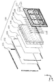
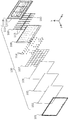
- the liquid crystal module 100 having the above configuration further includes a mold frame 104, an optical sheet unit 105, a diffusion plate 106, a luminance uniform plate 107, a reflection sheet 108, and an LED sheet. 109, a relay sheet 110, a lower frame 111, and support pins 112.
- the mold frame 104 supports a plurality of components (so-called backlight units) from the optical sheet unit 105 to the LED sheet 109 and the relay sheet 110 with the lower frame 111 interposed therebetween. In FIG. 3, the mold frame 104 is not shown.
- the optical sheet unit 105 is configured by stacking a plurality of two or three types of sheets having different optical characteristics.
- the optical sheet unit 105 includes a vertical prism sheet, a horizontal prism sheet, and a diffusion sheet.
- the diffusion plate 106 diffuses light incident from a plurality of LEDs (Light-Emitting Diodes) 113 disposed on the LED sheet 109 and serving as a light source of the image display device 10, and emits the light toward the display panel 102.
- LEDs Light-Emitting Diodes
- the luminance uniform plate 107 transmits light from the plurality of LEDs 113 arranged on the LED sheet 109 (hereinafter also referred to as emitted light) to the side where the diffusion plate 106 is present while increasing the uniformity of luminance that varies depending on the location.
- the uniform brightness plate 107 is a sheet-like member made of a resin such as PET (polyethylene terephthalate) that contains fine bubbles densely and has good light reflectivity.
- PET polyethylene terephthalate
- the uniform luminance plate 107 has a large number of holes having different diameters, that is, openings. More specifically, the diameter of the hole immediately above each LED 113 is extremely small, and the diameter of the hole farther from the nearest LED 113 is larger.
- a part of the light emitted from the LED 113 passes through these holes to the opposite side, that is, the side where the diffusion plate 106 is located (this disclosure also expresses that “light passes through the uniform luminance plate 107”).
- the uniform brightness plate 107 has the number, size, and distribution of these holes adjusted so that the transmission amount per unit area of light from a light source at a predetermined distance is made uniform. Smoothes the alignment characteristics of the emitted light.
- the light from the LED 113 whose orientation characteristics have been smoothed by the luminance uniform plate 107 is diffused by the diffusion plate 106 so as to further suppress the luminance unevenness, and then emitted toward the display panel 102.
- the reflection sheet 108 is a sheet in which holes having positions and sizes corresponding to the plurality of LEDs 113 arranged on the LED sheet 109 are provided, and reflects light on the entire front surface of the image display device 10. .
- the reflection sheet 108 rises from a flat portion having a substantially flat surface smaller than the effective area of the display panel 102 and from the ends of the four sides of the flat portion, and is an effective area of the display panel 102 as viewed from the front side of the image display device 10. And a side wall that reaches the outer edge, and has a shape that generally follows the lower frame 111 described below.
- the LED sheet 109 is a flexible printed circuit board (hereinafter referred to as FPC (Flexible Printed Circuits)) on which a plurality of LEDs 113 are arranged.
- the LED 113 is disposed on one of the two main surfaces of the sheet-like FPC, and a reflective layer that reflects light is disposed on the main surface on which the FPC LED is disposed, that is, the main surface on the front side of the image display device 10. It is formed.
- the plurality of LEDs 113 on the main surface of the LED sheet 109 are arranged in a matrix at substantially equal intervals so as to irradiate the widest possible range of the back surface of the display panel 102 with as little unevenness as possible.
- the relay sheet 110 is an FPC in which an electrical path for sending power, a control signal, and the like to each LED 113 arranged on the LED sheet 109 is formed. Further, in the relay sheet 110, similarly to the LED sheet 109, a reflective layer is formed on the main surface on the front side of the image display device 10.
- the lower frame 111 is a plate-like member formed of a thin sheet metal and is also referred to as a base plate, and supports the LED sheet 109 and the relay sheet 110.
- the lower frame 111 rises from a flat portion 111A having a substantially flat surface smaller than the effective area of the display panel 102, and from the outer edge of the flat portion 111A, that is, from the ends of the four sides. And a side wall portion 111B reaching the outer edge of the effective area of the display panel 102 as viewed from a certain side.
- the liquid crystal module 100 has the four sides on the back side that are relatively large chamfered from the thin rectangular parallelepiped in the front-rear direction (the direction along the z-axis). There is an appearance effect that looks thinner due to the shape.
- a plurality of LEDs 113 as light sources are arranged on the flat portion 111A of the lower frame 111. More specifically, the LED sheet 109 and the relay sheet 110 in which the plurality of LEDs 113 are arranged at substantially equal intervals are attached to the flat portion 111A. Thereafter, the reflection sheet 108 is further attached so that each LED 113 is exposed from the plurality of holes of the reflection sheet 108. The light emitted from each LED 113 is reflected directly or by the reflection layer and the reflection sheet 108 formed on the FPC, and is incident on the luminance uniform plate 107 on the front side of the image display device 10 with respect to each LED 113.
- the lower frame 111 further supports the backlight unit from the optical sheet unit 105 to the LED sheet 109 and the relay sheet 110 with the mold frame 104 interposed therebetween.
- the lower frame 111 may further have a structure for supporting each structure of the backlight unit.
- the lower frame 111 may have a cut-and-raised part that hangs the optical sheet unit 105 in the vicinity of the upper side when the image display device 10 is put into use.
- the optical sheet unit 105 is provided with, for example, a tab having a hole for hooking it.
- the plurality of support pins 112 shown in FIG. 3 are columnar members.
- Each support pin 112 has a tip end portion 112A which is an end portion on the opposite side to the end portion attached to the lower frame 111, and a flange-like flange portion 112B in the middle of the columnar shape in the longitudinal direction.
- the plurality of support pins 112 are attached to the flat portion 111A of the lower frame 111 through the reflection sheet 108, and support the reflection sheet 108 with the lower frame 111 interposed therebetween.
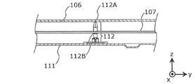
- FIG. 4 is a schematic diagram for explaining how the support pins 112 attached to the lower frame 111 support the diffusion plate 106 and the luminance uniform plate 107 inside the liquid crystal module 100.
- the configuration of the liquid crystal module 100 that is not necessary for this description is omitted.
- the brightness uniform plate 107 is provided with holes for inserting the support pins 112 at positions corresponding to the plurality of support pins 112 attached to the lower frame 111.
- the brightness uniform plate 107 is attached so that the support pin 112 is inserted into the hole from the tip end portion 112A and supported by the flange portion 112B of the support pin 112 as shown in FIG.
- the support pin 112 only needs to support the luminance uniform plate 107 at a certain appropriate distance from the lower frame 111 or the LED 113, which is determined by design, in the middle of the longitudinal direction.
- the configuration for this support is as follows.
- the flange shape is not limited to the flange portion 112B.
- the support pin 112 may have a base-like portion with a top surface instead of the flange portion 112B, and the luminance uniform plate 107 may be supported by the top surface of this portion.
- the support pin 112 has a portion that becomes thicker from the front to the back of the liquid crystal module 100 when attached, and supports the luminance uniform plate 107 at a place where the diameter of the hole of the luminance uniform plate 107 coincides with this portion. Also good.
- the diffusion plate 106 is supported by the end of the side wall 111B of the lower frame 111 in the periphery, and is erected on the flat portion 111A of the lower frame 111 as shown in FIG. It is supported by the tip 112A of the support pin 112.
- the support pins 112 are arranged in a substantially equidistant matrix so as to support the entire diffuser plate 106 and luminance uniform plate 107 in the flat portion 111A. Further, the support pin 112 is arranged at a position away from each LED 113, for example, on a straight line connecting two equidistant points from the two LEDs 113 adjacent in the matrix direction so as not to block the light toward the luminance uniform plate 107 as much as possible.
- the configuration of the liquid crystal module 100 for further improving the uniformity of luminance over the entire screen will be described below.
- FIG. 5 is a schematic cross-sectional view for explaining the configuration of the liquid crystal module 100 according to the first embodiment.
- FIG. 5 shows a partial cross section of the liquid crystal module 100 including a portion extending from the flat portion 111A of the lower frame 111 to the upper side wall portion 111B.
- the configuration of the liquid crystal module 100 is common even in a portion extending from the flat portion 111A to the lower side or the left and right side wall portions 111B.
- FIG. 6 is a schematic cross-sectional view of a comparative example used to explain the effects of the configuration of the liquid crystal module 100 according to the first embodiment.
- the illustration of the configuration of the liquid crystal module 100 that is not necessary for the description of the present embodiment is omitted.
- the configuration common to that shown in FIG. 4 is also shown by a simplified diagram in consideration of easy viewing.
- 5 and 6 indicate the position of the outer edge (upper end) on the upper side of the effective area of the display panel 102 as viewed from the lateral direction.
- the side wall portion 111B extends from the outer edge of the flat portion 111A and reaches the outer edge of the effective area of the display panel 102.
- the outer edge of the uniform luminance plate 107 also reaches the outer edge of the effective area. Further, although the whole cannot be grasped in the sectional view of FIG. 5, the outer edge of the uniform luminance plate 107 substantially coincides with the outer edge of the effective area, and the uniform luminance plate 107 covers the lower frame 111 to the end. Further, the uniform luminance plate 107 has a constant distance to the lower frame 111 from the flat portion 111A, but the side wall between the diffusion plate 106 and the side wall portion 111B extends from the outer edge of the flat portion 111A to the outer edge of the side wall portion 111B. This distance is gradually reduced by curving toward the portion 111B.
- the emitted light of the LED 113 is diffused through the luminance uniform plate 107 after being reflected directly or by the reflective sheet 108 on the lower frame 111 or the reflective layer of the LED sheet 109 in the entire effective area. Incident on the plate 106.
- the entire luminance uniform plate 107 is flat. Therefore, the distance between the uniform brightness plate 107 and the lower frame 111 is constant with the flat portion 111A, and the side wall portion 111B gradually decreases from the outer edge of the flat portion 111A toward the outside. However, the uniform luminance plate 107 does not reach the outer edge of the effective area of the display panel 102 and contacts the side wall portion 111B.
- the broken lines in FIG. 6 indicate the position in the vertical direction (on the y axis) where the luminance uniform plate 107 and the side wall portion 111B are in contact with each other and the position on the diffusion plate 106 corresponding to this position, as viewed from the lateral direction.
- the light incident on the region inside (shown by the white arrow) from the broken line has a smooth orientation characteristic by the uniform luminance plate 107.
- the light entering the diffuser 106 is in the inner area. Only the light that has traveled a certain distance after passing through the uniform luminance plate 107, and the incident light is weaker than the light incident on the inner region.
- This situation occurs in the four peripheral areas in the effective area of the display panel 102, and in the peripheral area of the screen, a luminance difference occurs depending on the presence or absence of the luminance uniform plate 107 directly below. Such a difference in brightness may appear on the screen as unevenness visible to the user.
- the outer dimension of the luminance uniform plate 107 is larger than that of the comparative example, and the outer edge thereof reaches the outer edge of the effective area of the display panel 102. Further, there is a space sandwiched between the luminance uniform plate 107 and the side wall portion 111B of the lower frame 111 from the rise of the side wall portion 111B to the very vicinity of the outer edge of the effective region, and the light from the LED 113 is emitted from the luminance uniform plate. Advancing while reflecting between 107 and the reflective sheet 108 along the lower frame 111, it reaches the very vicinity of the outer edge of the effective area.
- the light incident on the diffusion plate 106 is adjusted so that the intensity thereof is uniformly approached by the luminance uniform plate 107 located directly below the entire effective area of the display panel 102.
- the light incident on the diffusion plate 106 is stronger in the four peripheral areas in the effective area than in the configuration of FIG. 6, and the overall uniformity is high. Therefore, in liquid crystal module 100 according to the present embodiment, display with higher uniformity of luminance is possible from the center of the screen to the peripheral region.
- the image display device 10 includes a display panel 102, a lower frame 111, a plurality of LEDs 113 that are light sources, a plurality of columnar support pins 112, a plate-like diffusion plate 106, and a sheet. And a uniform luminance plate 107.
- the lower frame 111 includes a flat portion 111A having a substantially flat surface smaller than the effective area of the display panel 102, and a side wall portion 111B that rises from the outer edge of the flat portion 111A and reaches the outer edge of the effective area in a front view.
- the plurality of LEDs 113 are arranged in a matrix at substantially equal intervals on the flat portion 111A.
- the plurality of support pins 112 are arranged in a substantially equidistant matrix at positions on the flat portion 111 ⁇ / b> A that are distant from each of the plurality of LEDs 113.
- the diffusion plate 106 is supported by the front end portions 112 ⁇ / b> A of the plurality of support pins 112 and the lower frame 111.
- the diffusion plate 106 diffuses incident light emitted from the LEDs 113 and emits the light toward the display panel 102.
- the uniform luminance plate 107 is supported between the diffusion plate 106 and the lower frame 111 in the middle of the plurality of support pins 112, the outer edge substantially coincides with the outer edge of the effective area, and a part of the emitted light of the LED 113 is used.
- the diffusion plate 106 is transmitted to the side where it exists.
- the uniform luminance plate 107 is curved toward the side wall 111B between the diffusion plate 106 and the side wall 111B so that the distance from the lower frame 111 gradually decreases from the outer edge of the flat portion 111A to the outer edge of the side wall 111B.
- the light from the LED 113 can travel between the luminance uniform plate 107 and the lower frame 111 to the very vicinity of the outer edge of the effective area of the display panel 102.
- the light also passes through the luminance uniform plate 107 from the very vicinity of the outer edge of the effective region, enters the diffusion plate 106, is diffused by the diffusion plate 106, and is emitted toward the display panel 102.
- the image display apparatus 10 can perform display with higher uniformity of luminance from the center of the screen to the peripheral region.
- FIG. 7 is a schematic cross-sectional view for explaining the configuration of the liquid crystal module 100 according to the second embodiment.
- FIG. 7 shows a cross section of a part of the liquid crystal module 100 including a portion extending from the flat portion 111A of the lower frame 111 to the upper side wall portion 111B, as in FIG.
- the configuration of the liquid crystal module 100 that is not necessary for the description of the present embodiment is omitted.
- the configuration common to that shown in FIG. 4 is also shown by a simplified diagram in consideration of easy viewing.
- the wedge shape in FIG. 7 indicates the position of the outer edge (upper end) on the upper side of the effective area of the display panel 102 as viewed from the side as in FIG.
- the configuration of the liquid crystal module 100 is common even in a portion extending from the flat portion 111A to the lower side or the left and right side wall portions 111B.
- the light from the LED 113 is allowed to reach the peripheral region by a configuration in which the light is advanced while being reflected between the luminance uniform plate 107 and the reflection sheet 108.
- the luminance uniform plate 107 in order to allow the light from the LED 113 to reach the peripheral region, the luminance uniform plate 107 having a smaller outer dimension than that of the comparative example shown in FIG. A gap is provided between the uniform plate 107 and the side wall 111B of the lower frame 111 for allowing light to pass through.
- a white arrow in FIG. 7 indicates a path through which light from the LED 113 enters the peripheral region.
- the light from the LED 113 wraps around the uniform luminance plate 107 into the peripheral area of the liquid crystal module 100.
- the liquid crystal module 100 can display with higher uniformity of luminance from the center of the screen to the peripheral region.
- FIG. 8 is a schematic cross-sectional view for explaining the configuration of the liquid crystal module 100 according to the third embodiment.
- FIG. 8 shows a cross section of a part of the liquid crystal module 100 including a portion extending from the flat portion 111 ⁇ / b> A of the lower frame 111 to the upper side wall portion 111 ⁇ / b> B, as in FIGS. 5 and 7.
- the configuration of the liquid crystal module 100 that is not necessary for this explanation is omitted.
- the configuration common to that shown in FIG. 4 is also shown by a simplified diagram in consideration of easy viewing.
- the configuration of the liquid crystal module 100 is common even in a portion extending from the flat portion 111A to the lower side or the left and right side wall portions 111B.
- the side wall portion 111B of the lower frame 111 has a standing wall 1110 that stands up toward the diffusion plate 106 starting from the outer edge thereof. Further, the outer edge of the uniform luminance plate 107 reaches the outer edge of the side wall portion 111B and substantially coincides with the starting point of the standing wall 1110. Accordingly, as compared with the liquid crystal module 100 shown in FIG. 5, a distance substantially equal to the height of the standing wall 1110 (dimension in the z-axis direction) is ensured between the diffusion plate 106 and the luminance uniform plate 107.
- the outer edge of the luminance uniform plate 107 reaches very close to the diffusion plate 106 in the vicinity of the outer edge of the effective area of the display panel 102.
- the shadow of the uniform luminance plate 107 falls on the diffusion plate 106 near the outer edge of the effective area, and the difference in brightness between the shadow and the portion other than the shadow appears on the screen as luminance unevenness that can be visually recognized by the user. Can appear.
- the standing wall 1110 may be positioned substantially immediately below the effective area of the display panel 102. More preferably, the standing wall 1110 may be positioned outside the effective area by about 1 to 2 millimeters. As a result, the entire display panel 102 can be more reliably included in the irradiation range of the light transmitted through the uniform luminance plate 107.
- the light from the LED 113 travels while reflecting between the reflective sheet 108 along the uniform luminance plate 107 and reaches the very vicinity of the outer edge of the effective area.
- the occurrence of a shadow of the uniform luminance plate 107 falling on the diffusion plate 106 is prevented or the shadow is thinned.
- the liquid crystal module 100 according to the present embodiment enables display with higher uniformity of luminance from the center of the screen to the peripheral region.
- the dimensions of the standing wall 1110 for example, when the distance between the lower frame 111 and the diffusion plate 106 is 20 millimeters, and the distance between the lower frame 111 and the luminance uniform plate 107 is 10 millimeters, the height 3 A standing wall 1110 on the order of millimeters may be provided. However, these dimensions are changed in design for adjustment according to the overall size of the liquid crystal module 100 or the required appearance, the density or light emission intensity of the LEDs 113 to be arranged, and the like.
- the configuration of the liquid crystal module 100 is not limited.
- the standing wall 1110 is higher, the effect of suppressing the shadow of the luminance uniform plate 107 on the diffusion plate 106 is further increased, but the image display device 10 is difficult to show thinly.
- the height of the standing wall 1110 is preferably determined in consideration of this point.
- the side wall portion 111B has the standing wall 1110 that stands up toward the diffusion plate 106 with the outer edge as a starting point, and the outer edge of the luminance uniform plate 107 is the diffusion plate 106. It almost coincides with the starting point of.
- an interval corresponding to the height of the standing wall 1110 is ensured between the diffusion plate 106 and the outer edge closest to the diffusion plate 106 in the luminance uniform plate 107.
- the image display device 10 can display with higher uniformity of luminance from the center of the screen to the peripheral region.
- the curved shape of the uniform luminance plate 107 in Embodiment 1 or 3 may be the shape of the formed uniform luminance plate 107 itself.
- Such a shape may be provided by bending the outer edge of the lower frame 111 against the lower frame 111. In this case, the luminance uniform plate 107 is stretched against the lower frame 111 by its own elasticity and supported by the lower frame 111.
- FIG. 9 is a schematic cross-sectional view for explaining such bending that occurs in the liquid crystal module 100 according to the third embodiment.
- FIG. 9 shows a cross section of a part of the liquid crystal module 100 including a portion extending from the flat portion 111A of the lower frame 111 to the upper side wall portion 111B, as in FIG.
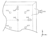
- FIG. 10 is a schematic cross-sectional view for explaining the configuration of the liquid crystal module 100 according to this modification.
- FIG. 11 is a schematic front view for explaining the configuration of the liquid crystal module 100 according to this modification.
- FIG. 10 shows a cross section of a part of the liquid crystal module 100 including a portion extending from the flat portion 111A of the lower frame 111 to the upper side wall portion 111B, as in FIG. 9 and the like.
- FIG. 11 shows a part including the upper right corner of the lower frame 111 as viewed from the front (side with the display panel 102).
- illustrations of the configuration of the liquid crystal module 100 that are not necessary for the description of this modification are omitted.
- FIG. 4 is also shown by a simplified diagram in consideration of easy viewing.
- the broken lines in FIG. 11 indicate valley-folded portions, and the alternate long and short dash lines are virtual straight lines that connect points that are equidistant from the two LEDs 113 adjacent in the matrix direction.
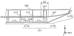
- the liquid crystal module 100 further includes a columnar auxiliary support pin 114 on an imaginary straight line (the one-dot chain line in FIG. 11) on which the support pin 112 is arranged.
- the auxiliary support pins 114 also support the luminance uniform plate 107 between the diffusion plate 106 and the lower frame 111.
- the position in the z-axis direction where the auxiliary support pin 114 supports the luminance uniform plate 107, in other words, the height from the lower frame 111 is the same as the height supported by the support pin 112.
- the set of auxiliary support pins 114 is closer to the outer edge of the flat portion 111A than the plurality of support pins 112 and the plurality of LEDs 113. . Further, the interval between the pair of auxiliary support pins 114 is narrower than the interval between the plurality of support pins 112.
- the auxiliary support pins 114 are arranged in the flat portion 111A at a position closer to the outer edge of the flat portion 111A than the plurality of LEDs 113, and the continuous flat range without deflection in the uniform luminance plate 107 is arranged in a matrix. This is because a plurality of LEDs 113 are directly underneath, and are secured in a wider inner region. In this modification, as shown in FIG. 10, the bending of the luminance uniform plate 107 is suppressed in a narrower range (double arrow D3 in FIG. 10) outside this region.
- auxiliary support pins 114 are arranged on the above-described straight line by extending as far as possible from any of the LEDs 113 so that the auxiliary support pins 114 can block light from the LEDs 113 and extend toward the side wall 111B. This is to minimize the influence of shadows.
- the liquid crystal module 100 according to the present modification can display with higher uniformity of luminance from the center of the screen to the peripheral region.
- auxiliary support pins 114 are used as one set.
- three or more auxiliary support pins 114 may be used as a set according to the necessity for suppressing bending.
- the shadow generated by the auxiliary support pin 114 blocking the light from the LED 113 affects the uniformity of the luminance, so that it is desirable that the amount be as small as possible.
- auxiliary support pins may be interpreted as a set of auxiliary support pins 114.
- the interval between the auxiliary support pins may not be uniform.
- the auxiliary support pins 114 support the luminance uniform plate 107 at a predetermined height from the lower frame 111 in order to suppress the deflection of the luminance uniform plate 107, and the support pin 112 supports the luminance uniform plate 107 at this height. It is common with the height to do.
- the diffusion plate 106 need not be supported by all the auxiliary support pins 114 unlike the support pins 112.
- the auxiliary support pins 114 other than one of the set of auxiliary support pins 114 have a height and structure for supporting the luminance uniform plate 107, for example, two flanges sandwiching the luminance uniform plate 107 at a predetermined height. And may be shorter than the support pin 112.
- the amount of the light transmitted through the uniform luminance plate 107 blocked by the auxiliary support pins 114 can be suppressed to the same level as the configuration without the auxiliary support pins 114 as shown in FIG.
- the shape of the auxiliary support pin 114 may not be the same as that of the support pin 112, and may be thinner than the support pin 112, for example. Thereby, the influence of the shadow which falls on the side wall part 111B can be suppressed more.
- the above-described configuration described as a modification of the third embodiment can also be applied as a modification of the first embodiment.
- the amount of bending (the difference in height in the z-axis direction) of the luminance uniform plate 107 in the peripheral region is larger.
- the amount of deflection can be large. Therefore, by providing the auxiliary support pins 114 and suppressing the bending, the liquid crystal module 100 can display with higher uniformity of luminance from the center of the screen to the peripheral region.
- the plurality of support pins 112 are positioned on a straight line connecting points that are equidistant from the two LEDs 113 that are adjacent in the matrix direction among the plurality of LEDs 113 that are light sources.
- the image display device 10 further includes the luminance uniform plate 107 and the lower frame 111 and the diffusion plate at a position on the straight line and closer to the outer edge of the flat portion 111A than the plurality of support pins 112 and the plurality of LEDs 113.
- a pair of columnar auxiliary support pins 114 that support at least one pair are provided. The distance between the pair of auxiliary support pins 114 is narrower than the distance between the plurality of support pins 112.
- the bending amount of the bending that may occur due to the stress on the luminance uniform plate 107 is suppressed by the auxiliary support pins 114.
- the auxiliary support pins 114 are positioned near the outer edge of the uniform brightness plate 107, a flat area that is wider and continuous in the uniform brightness plate 107 is obtained.
- the image display device 10 can perform display with higher uniformity of luminance in a region that extends from the center to the periphery of the screen.
- each of the above-described embodiments and modification examples can be applied to a direct backlight type image display apparatus using a light source other than LEDs.
- the light source other than the LED of the image display device to which each embodiment or modification is applied include a cold cathode tube and a fluorescent tube.
- the reflection sheet 108 supported by being sandwiched between the support pin 112 and the lower frame 111 is described.
- the configuration is not limited to this.
- the entire front surface of the lower frame 111 may be coated with a material having a high light reflectance, or the lower frame 111 itself may be made of a material having a high light reflectance.
- the reflection sheet 108 as the reflection material and the lower frame 111 may be identified with each other.
- the distance between the luminance uniform plate 107 and the lower frame 111 in the above description is the same as the luminance uniform plate 107 and the reflection sheet 108. Can be interpreted synonymously with the distance.
- image display device 10 has been described as a liquid crystal television, for example, other examples include a monitor display for a personal computer and a display for digital signage.
- the present disclosure can be applied to an image display device having an appearance that looks thinner, for example, by suppressing the thickness of the peripheral portion from other portions. More specifically, the present disclosure is applicable to a television receiver, a monitor display, a digital signage display, or the like.
- Image display apparatus 100 Liquid crystal module 101 Bezel 102 Display panel 103 Back cover 104 Mold frame 105 Optical sheet unit 106 Diffuser plate 107 Brightness uniform plate 108 Reflective sheet 109 LED sheet 110 Relay sheet 111 Lower frame 111A Flat part 111B Side wall part 112 Support pin 112A tip 112B flange 113 LED (light source) 114 Auxiliary support pin 200 Stand 1110 Standing wall
Abstract
画像表示装置(10)は、表示パネル(102)と、平坦部(111A)及び側壁部(111B)を含む下フレーム(111)と、平坦部(111A)に行列状に配置される光源(113)と、光源(113)とは離れた平坦部(111A)上の位置で行列状に配置されるサポートピン(112)と、光源(113)の出射光を拡散して表示パネル(102)に向けて出射する拡散板(106)と、サポートピン(112)の途中で拡散板(106)と下フレーム(111)との間に支持され、外縁が表示パネル(102)の有効領域の外縁と略一致し、光源(113)の出射光の一部を拡散板(106)がある側に透過させる輝度均一板(107)とを備え、輝度均一板(107)は、下フレーム(111)との距離が平坦部(111A)の外縁から側壁部(111B)の外縁にかけて漸減するよう、拡散板(106)と側壁部(111B)との間で側壁部(111B)側に湾曲する。
Description
本開示は、液晶セル等の表示パネルを備える画像表示装置に関する。
特許文献1は、輝度ムラが少ない均一な面照明光を得るための光透過反射板を含む面光源ユニットを直下型のバックライトとして用いる表示装置を開示する。
本開示は、薄く見える外観を備え、かつ画面全体で輝度の均一性のより高い表示が可能な画像表示装置を提供する。
本開示における画像表示装置は、表示パネルと、表示パネルの有効領域より小さい略平坦な面を有する平坦部、及び当該平坦部の外縁から立ち上がり、正面視において上記の有効領域の外縁に達する側壁部を含む下フレームと、平坦部に略等間隔で行列状に配置される複数の光源と、複数の光源のそれぞれとは離れた平坦部上の位置で、略等間隔の行列状に配置される、柱状の複数のサポートピンと、複数のサポートピンの先端部及び下フレームで支持され、入射する複数の光源の出射光を拡散して表示パネルに向けて出射する板状の拡散板と、複数のサポートピンの途中で、拡散板と下フレームとの間に支持され、外縁が上記の有効領域の外縁と略一致し、複数の光源の出射光の一部を拡散板がある側に透過させるシート状の輝度均一板とを備え、輝度均一板は、下フレームとの距離が平坦部の外縁から側壁部の外縁にかけて漸減するよう、拡散板と側壁部との間で側壁部側に湾曲する。
本開示における画像表示装置によれば、薄く見える外観を備え、かつ画面全体で輝度の均一性のより高い表示が可能である。
本願発明者は、従来の画像表示装置に関し、以下の問題が生じることを見出した。
従来の液晶テレビ等の画像表示装置では、表示パネルを取り囲むように含む表示モジュールは、大まかには前後に薄い直方体であるが、より厳密には、その背面側の四辺が比較的大きく面取りされたような形状を有する。このような端面での厚さの小さい形状とすることで、表示モジュールそのものを薄く見せるという外観上の効果を得ている。
このような形状の表示モジュールの内部では、周辺部分の厚さがその他の部分に比べて小さい。
ところがこのような画像表示装置では、周辺部分においては内部空間の厚さ方向の制約上、その他の部分と共通の表示機構が採用できない。そのため、画面全体で均一な画質を得るのが困難であるという問題がある。より具体的には、直下型バックライト方式を用いる画像表示装置では、画面の中心から周辺にわたって均一な輝度を得るのが困難な場合がある。
本開示はこのような知見に基づいてなされたものであり、本願発明者は、上記のような外観に関する要求に応えつつ、かつ、画面全体で輝度の均一性のより高い表示が可能な画像表示装置の構造の着想を得た。
以下、適宜図面を参照しながら実施の形態を説明する。ただし、必要以上に詳細な説明は省略する場合がある。例えば、既によく知られた事項の詳細説明や実質的に同一の構成に対する重複説明を省略する場合がある。これは、以下の説明が不必要に冗長になるのを避け、当業者の理解を容易にするためである。
なお、本願発明者は、当業者が本開示を十分に理解するために添付図面および以下の説明を提供するのであって、これらによって請求の範囲に記載の主題を限定することを意図するものではない。
以下、液晶テレビを構成する画像表示装置を例に用いて、図を参照して複数の実施の形態について説明するが、それに先立って、各実施の形態及びその変形例に共通して関連する画像表示装置の構造の概要について説明する。実施の形態間での差異は後述する。
また、以下の実施の形態において、説明の便宜上、画像表示装置の上下方向をy軸の方向と一致させ、前後方向をz軸の方向と一致させ、左右方向をx軸の方向と一致させているが、方向のこれらの対応付けは、本開示に係る画像表示装置の製造時又は使用時における姿勢を限定するものではない。
(画像表示装置の構成概要)
図1は、各実施の形態に係る画像表示装置10の外観斜視図である。図2及び図3はそれぞれ、各実施の形態に係る液晶モジュール100の分解斜視図である。
図1は、各実施の形態に係る画像表示装置10の外観斜視図である。図2及び図3はそれぞれ、各実施の形態に係る液晶モジュール100の分解斜視図である。
画像表示装置10は例えば液晶テレビであり、図1に示されるように、液晶モジュール100と、ベゼル101と、バックカバー103と、スタンド200とを備える。
液晶モジュール100は静止画及び動画を表示可能な映像表示のためのモジュールであり、表示パネル102を備える。
表示パネル102は、以下に説明する各実施の形態では、いわゆる液晶セルであり、複数のガラス板の間に液晶が封入された素子である。表示パネル102は、画像表示装置10に入力された映像信号に基づいて制御され、映像を表示する。
また、液晶モジュール100はスタンド200を用いて、床又は台の上に立てることができる。ただし、液晶モジュール100は、スタンド200を用いずに、他の取付具を用いて壁に掛けられるか又は埋め込まれたり、天井から吊り下げられたりしての画像表示装置10としての使用が可能であってもよい。
樹脂で形成されるベゼル101は、画像表示装置10の四辺それぞれに対応するよう分割して形成され、例えばネジを用いて相互に結合される。ベゼル101は、後述の表示パネル102から下フレーム111までの複数の部品を、バックカバー103と共に挟持する。
上記構成を有する液晶モジュール100はさらに、図2又は図3に示されるように、モールドフレーム104と、光学シートユニット105と、拡散板106と、輝度均一板107と、反射シート108と、LEDシート109と、中継シート110と、下フレーム111と、サポートピン112とを備える。
モールドフレーム104は、光学シートユニット105からLEDシート109及び中継シート110までの複数の部品(いわゆるバックライトユニット)を、下フレーム111と挟んで支持する。なお、図3ではモールドフレーム104の図示を省略している。
光学シートユニット105は、光学特性の異なる2、3種類のシートを複数枚重ねて構成される。例えば、光学シートユニット105には、縦方向のプリズムシート、横方向のプリズムシート及び拡散シートが含まれる。
拡散板106は、LEDシート109上に配置された、画像表示装置10の光源である複数のLED(Light-Emitting Diode)113から入射する光を拡散して、表示パネル102に向けて出射する。
輝度均一板107は、LEDシート109上に配置された複数のLED113からの光(以下、出射光ともいう)を、場所によって異なる輝度の均一度を高めて拡散板106がある側に透過させる。輝度均一板107は、例えば微細な気泡を密に含むPET(polyethylene terephthalate)等の樹脂製で、良好な光反射性を有するシート状の部材である。また、輝度均一板107には、径の異なる孔、つまり開口が全体にわたって多数形成されている。より具体的には、各LED113の直上にある孔の径は極めて小さく、最寄りのLED113から遠い孔ほど径が大きい。LED113の出射光は、その一部がこれらの孔を通って反対側、つまり拡散板106のある側に抜ける(本開示では「光が輝度均一板107を透過する」とも表現している)。輝度均一板107は、所定の距離にある光源からの光の単位面積当たりの透過量を均一に近づけるようにこれらの孔の個数、大きさ及び分布が調整されており、この構成によって、各LED113が出射した光の配向特性をなだらかにする。輝度均一板107によって配向特性がなだらかにされたLED113からの光は、拡散板106によって輝度ムラがさらに抑えられるよう拡散されてから表示パネル102に向けて出射される。
反射シート108は、LEDシート109上に配置された複数のLED113のそれぞれに対応する位置及び大きさの孔が設けられたシートであり、画像表示装置10の正面側の面全体で光を反射する。反射シート108は、表示パネル102の有効領域より小さい略平坦な面を有する平坦部と、平坦部の四辺の端部から立ちあがり、画像表示装置10の正面側から見て表示パネル102の有効領域の外縁に達する側壁部とを含み、全体として後述の下フレーム111に概ね沿う形状を有する。
LEDシート109は、複数のLED113が配置されたフレキシブルプリント基板(以下、FPC(Flexible Printed Circuitsの頭字語)という)である。LED113はシート状のFPCの2つの主面の一方に配置され、FPCのLEDが配置されている主面、つまりは画像表示装置10の正面側の主面には、光を反射する反射層が形成される。また、LEDシート109の主面にある複数のLED113は、表示パネル102の背面の極力広い範囲を、場所によるムラを極力抑えて照射できるよう、略等間隔で行列状に配置される。
中継シート110は、LEDシート109に配置されている各LED113へ電力や制御信号などを送るための電気経路が形成されたFPCである。また、中継シート110では、LEDシート109と同様に、画像表示装置10の正面側の主面に反射層が形成される。
下フレーム111は薄い板金で形成される板状の部材であってベースプレートとも称され、LEDシート109及び中継シート110を支持する。下フレーム111は、表示パネル102の有効領域より小さい略平坦な面を有する平坦部111Aと、平坦部111Aの外縁、つまり四辺の端部から立ちあがり、画像表示装置10の正面側(表示パネル102のある側)から見て表示パネル102の有効領域の外縁に達する側壁部111Bとを含む。バックカバー103を下フレーム111の外形に沿った形状にすることで、液晶モジュール100は上述の、前後(z軸に沿う方向)に薄い直方体から背面側の四辺が比較的大きく面取りされたような形状による、より薄く見えるという外観上の効果を奏している。
また、下フレーム111の平坦部111Aには、光源である複数のLED113が配置される。より具体的には、複数のLED113が略等間隔で配置されたLEDシート109及び中継シート110が平坦部111Aに取り付けられる。その後、さらに反射シート108が、反射シート108の複数の孔から各LED113が露出するように貼り付けられる。各LED113の出射光は、直接、又はFPCに形成された反射層及び反射シート108によって反射されて、各LED113に対して画像表示装置10の正面側にある輝度均一板107に入射する。下フレーム111はさらに、光学シートユニット105からLEDシート109及び中継シート110までのバックライトユニットを、モールドフレーム104と挟んで支持する。
下フレーム111はバックライトユニット各構成を支持するための構成をさらに有してもよい。例えば、下フレーム111には、画像表示装置10を使用状態に置いたときに上側となる一辺の近辺に、光学シートユニット105を吊り下げる切り起こしが形成されていてもよい。この場合、光学シートユニット105には、例えばこの切り起こしに引っ掛けるための孔を有するタブが設けられる。
図3に示される複数のサポートピン112は、柱状の部材である。各サポートピン112は、下フレーム111に取り付けられる端部と反対側の端部である先端部112Aと、柱状の形状の長手方向の途中にある鍔状のフランジ部112Bを有する。
複数のサポートピン112は、反射シート108越しに下フレーム111の平坦部111Aに取り付けられ、反射シート108を下フレーム111と挟んで支持する。
また、複数のサポートピン112は、拡散板106及び輝度均一板107を支持する。図4は、液晶モジュール100の内部で下フレーム111に取り付けられたサポートピン112が拡散板106及び輝度均一板107を支持する様子を説明するための模式図である。ただし、図4では、液晶モジュール100の構成のうち、この説明に必要ないものは図示を省略している。
輝度均一板107には、下フレーム111に取り付けられた複数のサポートピン112のそれぞれに対応する位置に、サポートピン112を挿入するための孔が設けられている。輝度均一板107は、この孔にサポートピン112が先端部112Aから挿入されて、図4に示されるように、サポートピン112のフランジ部112Bで支持されるように取り付けられる。
なお、サポートピン112はその長手方向の途中で、設計上決定される、下フレーム111又はLED113から一定の適切な距離の位置に輝度均一板107を支持すればよく、この支持のための構成は、鍔状のフランジ部112Bに限定されない。例えばサポートピン112は、フランジ部112Bに代えて頂面のある台座のような部分を有し、この部分の頂面で輝度均一板107を支持してもよい。または、サポートピン112は、取付時に液晶モジュール100の正面から背面に向かって太くなる部分を有し、この部分と輝度均一板107の孔の径が一致する場所で輝度均一板107を支持してもよい。
また、拡散板106は、周辺において下フレーム111の側壁部111Bの端部で支持されるとともに、周辺以外の部分では、図4に示されるように、下フレーム111の平坦部111Aに立設するサポートピン112の先端部112Aで支持される。
このようなサポートピン112は、平坦部111Aにおいて、拡散板106及び輝度均一板107の全体を支えられるよう、略等間隔の行列状に配置される。また、輝度均一板107に向かう光を極力遮らないよう、サポートピン112は、各LED113から離れた位置、例えば、行列方向に隣接する2個のLED113から等距離の点を結ぶ直線上に配置される。
このような本開示に係る画像表示装置10において、画面全体で輝度の均一性をより高めるための液晶モジュール100の構成を以下に説明する。
(実施の形態1)
図5は、実施の形態1に係る液晶モジュール100の構成を説明するための模式断面図である。図5に示されるのは、下フレーム111の平坦部111Aから上側の側壁部111Bに跨る部分を含む液晶モジュール100の一部の断面である。平坦部111Aから下側又は左右の側壁部111Bに跨る部分でも液晶モジュール100の構成は共通である。
図5は、実施の形態1に係る液晶モジュール100の構成を説明するための模式断面図である。図5に示されるのは、下フレーム111の平坦部111Aから上側の側壁部111Bに跨る部分を含む液晶モジュール100の一部の断面である。平坦部111Aから下側又は左右の側壁部111Bに跨る部分でも液晶モジュール100の構成は共通である。
図6は、実施の形態1に係る液晶モジュール100の構成の効果を説明するために用いる比較例の模式断面図である。ただし、図5及び図6では、液晶モジュール100の構成のうち、本実施の形態の説明に必要ないものは図示を省略している。また、図4までと共通の構成も、見やすさを考慮してより簡略化した図形で示している。
図5及び図6中の楔形は、横方向から見た表示パネル102の有効領域の上側の外縁(上端)の位置を指す。上述のとおり、側壁部111Bは、平坦部111Aの外縁から延在して表示パネル102の有効領域の外縁に達する。
図5に示されるように、輝度均一板107もまた、その外縁が上記の有効領域の外縁に達する。また、図5の断面図では全体が把握できないが、輝度均一板107の外縁は上記の有効領域の外縁と略一致しており、輝度均一板107は下フレーム111を端まで覆う。さらに、輝度均一板107は、下フレーム111との距離が平坦部111Aとは一定であるが、平坦部111Aの外縁から側壁部111Bの外縁にかけて、拡散板106と側壁部111Bとの間で側壁部111B側に湾曲してこの距離が漸減する。この構成により、LED113の出射光は、上記有効領域の全域において、直接又は下フレーム111の上にある反射シート108若しくはLEDシート109の反射層に反射されてから輝度均一板107を透過して拡散板106に入射する。
ここで、図5に示される構成の効果を説明するために、図6に示される構成と比較する。図6の構成では、輝度均一板107は全体が平坦である。したがって、輝度均一板107と下フレーム111との距離が、平坦部111Aとは一定であり、側壁部111Bとは平坦部111Aの外縁から外側に向かって漸減する。ただし、輝度均一板107は表示パネル102の有効領域の外縁に達することなく、側壁部111Bと接触する。図6の破線は、横方向から見た、輝度均一板107と側壁部111Bとが接触する上下方向(y軸上)の位置、及びこの位置に対応する拡散板106上の位置を示す。
拡散板106に入射する光のうち、この破線より内側(白い矢印で示される側)の領域に入射する光は、輝度均一板107によって配向特性がなだらかにされている。これに対し、この破線より外側(ハッチングが施された矢印で示される側)の領域に輝度均一板107を透過する前に到達する光はなく、拡散板106に入射するのは内側の領域で輝度均一板107を透過後にある程度の距離を進んだ光のみであり、内側の領域に入射する光に比べて入射光は弱い。この状況は、表示パネル102の有効領域における四方の周辺領域で発生し、画面の周辺領域では直下の輝度均一板107の有無に輝度差が生じる。このような明るさの差は、ユーザが視認可能なムラとなって画面に現れ得る。
一方、図5に示される本実施の形態における構成では、輝度均一板107の外形寸法が比較例よりも大きく、その外縁は表示パネル102の有効領域の外縁に達する。また、側壁部111Bの立ち上がりから当該有効領域の外縁の極近傍に至るまで、輝度均一板107と下フレーム111の側壁部111Bとに挟まれた空間があり、LED113からの光は、輝度均一板107と下フレーム111に沿う反射シート108との間を反射しながら進んで上記の有効領域の外縁の極近傍にまで到達する。また、拡散板106に入射する光は、表示パネル102の有効領域全体で直下にある輝度均一板107によって強さが一様に近づくよう調整されている。これにより、拡散板106に入射する光は図6の構成に比べて有効領域における四方の周辺領域でより強く、全体では均一性が高い。したがって、本実施の形態に係る液晶モジュール100では、画面の中心から周辺領域にわたって輝度の均一性のより高い表示が可能である。
上述した本実施の形態に係る画像表示装置10は、表示パネル102と、下フレーム111と、光源である複数のLED113と、柱状の複数のサポートピン112と、板状の拡散板106と、シート状の輝度均一板107とを備える。下フレーム111は、表示パネル102の有効領域より小さい略平坦な面を有する平坦部111A、及び平坦部111Aの外縁から立ち上がり、正面視において上記の有効領域の外縁に達する側壁部111Bを含む。複数のLED113は、平坦部111Aに略等間隔で行列状に配置される。複数のサポートピン112は、複数のLED113のそれぞれとは離れた平坦部111A上の位置で略等間隔の行列状に配置される。拡散板106は、複数のサポートピン112の先端部112A及び下フレーム111で支持され、入射するLED113の出射光を拡散して表示パネル102に向けて出射する。輝度均一板107は、複数のサポートピン112の途中で、拡散板106と下フレーム111との間に支持され、外縁が上記の有効領域の外縁と略一致し、LED113の出射光の一部を拡散板106がある側に透過させる。また、輝度均一板107は、下フレーム111との距離が平坦部111Aの外縁から側壁部111Bの外縁にかけて漸減するよう、拡散板106と側壁部111Bとの間で側壁部111B側に湾曲する。
このような画像表示装置10では、LED113からの光は輝度均一板107と下フレーム111との間を、表示パネル102の有効領域の外縁の極近傍まで進むことができる。そして光は、有効領域の外縁の極近傍からも輝度均一板107を透過して拡散板106に入射し、拡散板106で拡散されて表示パネル102に向かって出射される。これにより、画像表示装置10は、画面の中心から周辺領域にわたって輝度の均一性のより高い表示が可能である。
(実施の形態2)
図7は、実施の形態2に係る液晶モジュール100の構成を説明するための模式断面図である。図7に示されるのは、図5と同様に、下フレーム111の平坦部111Aから上側の側壁部111Bに跨る部分を含む液晶モジュール100の一部の断面である。ただし、図7では、液晶モジュール100の構成のうち、本実施の形態の説明に必要ないものは図示を省略している。また、図4までと共通の構成も、見やすさを考慮してより簡略化した図形で示している。図7中の楔形は、図5と同様に、横方向から見た表示パネル102の有効領域の上側の外縁(上端)の位置を指す。平坦部111Aから下側又は左右の側壁部111Bに跨る部分でも液晶モジュール100の構成は共通である。
図7は、実施の形態2に係る液晶モジュール100の構成を説明するための模式断面図である。図7に示されるのは、図5と同様に、下フレーム111の平坦部111Aから上側の側壁部111Bに跨る部分を含む液晶モジュール100の一部の断面である。ただし、図7では、液晶モジュール100の構成のうち、本実施の形態の説明に必要ないものは図示を省略している。また、図4までと共通の構成も、見やすさを考慮してより簡略化した図形で示している。図7中の楔形は、図5と同様に、横方向から見た表示パネル102の有効領域の上側の外縁(上端)の位置を指す。平坦部111Aから下側又は左右の側壁部111Bに跨る部分でも液晶モジュール100の構成は共通である。
以下、実施の形態1又は図6に示した比較例との差異を中心に説明する。
図7に示されるように、実施の形態2に係る液晶モジュール100では、輝度均一板107と下フレーム111の側壁部111Bとの間に隙間がある。
上述のように、比較例では、LED113からの光で画像表示装置10の画面の周辺領域に到達するのは、輝度均一板107を透過した光のみである。また、実施の形態1では、LED113からの光を輝度均一板107と反射シート108との間を反射しながら進ませる構成によって周辺領域にも光を到達させている。
これに対し、実施の形態2に係る液晶モジュール100では、LED113からの光を周辺領域まで到達させるために、図6に示される比較例よりさらに外形寸法の小さい輝度均一板107を採用し、輝度均一板107と下フレーム111の側壁部111Bとの間に光を通過させるための隙間を設けている。図7における白い矢印は、LED113からの光が周辺領域に入る経路を示す。
これにより、液晶モジュール100の周辺領域に、LED113から光が輝度均一板107を回り込んで入る。この光によって、LED113から遠い周辺領域における明るさが補償される結果、液晶モジュール100は、画面の中心から周辺領域にわたって輝度の均一性のより高い表示が可能となる。
(実施の形態3)
図8は、実施の形態3に係る液晶モジュール100の構成を説明するための模式断面図である。図8に示されるのは、図5及び図7と同様に、下フレーム111の平坦部111Aから上側の側壁部111Bに跨る部分を含む液晶モジュール100の一部の断面である。ただし、図8では、液晶モジュール100の構成のうち、この説明に必要ないものは図示を省略している。また、図4までと共通の構成も、見やすさを考慮してより簡略化した図形で示している。図8中の楔形は、図5及び図7と同様に、横方向から見た表示パネル102の有効領域の上側の外縁(上端)の位置を指す。平坦部111Aから下側又は左右の側壁部111Bに跨る部分でも液晶モジュール100の構成は共通である。
図8は、実施の形態3に係る液晶モジュール100の構成を説明するための模式断面図である。図8に示されるのは、図5及び図7と同様に、下フレーム111の平坦部111Aから上側の側壁部111Bに跨る部分を含む液晶モジュール100の一部の断面である。ただし、図8では、液晶モジュール100の構成のうち、この説明に必要ないものは図示を省略している。また、図4までと共通の構成も、見やすさを考慮してより簡略化した図形で示している。図8中の楔形は、図5及び図7と同様に、横方向から見た表示パネル102の有効領域の上側の外縁(上端)の位置を指す。平坦部111Aから下側又は左右の側壁部111Bに跨る部分でも液晶モジュール100の構成は共通である。
以下、実施の形態1との差異を中心に説明する。
図8に示されるように、実施の形態3に係る液晶モジュール100では、下フレーム111の側壁部111Bが、その外縁を起点として拡散板106に向かって立設する立ち壁1110を有する。また、輝度均一板107の外縁は、側壁部111Bの外縁に到達して立ち壁1110の起点と略一致する。これにより、図5に示される液晶モジュール100と比較して、拡散板106と輝度均一板107との間に立ち壁1110の高さ(z軸方向の寸法)に略等しい距離が確保される。
実施の形態1の構成では、表示パネル102の有効領域の外縁近傍で、輝度均一板107の外縁が拡散板106の極近くに達する。この場合、この有効領域の外縁近傍で、輝度均一板107の影が拡散板106に落ち、この影と影以外の部分との明るさの差は、ユーザが視認可能な輝度のムラとして画面に現れ得る。しかし、上記の構成によって拡散板106と輝度均一板107との間に所定の距離を確保することで、拡散板106に落ちる輝度均一板107の影の発生を防ぐか、又は少なくともこのような影を薄くすることができる。
立ち壁1110は、表示パネル102の有効領域の略直下に位置してもよい。また、より望ましくは、立ち壁1110は当該有効領域から1~2ミリメートル程度外側に位置してもよい。これにより、表示パネル102全体を、輝度均一板107を透過した光の照射範囲に、より確実に包含させることができる。
実施の形態3に係る液晶モジュール100においても、LED113からの光は、輝度均一板107に沿う反射シート108との間を反射しながら進んで上記の有効領域の外縁の極近傍にまで到達する。その一方で、拡散板106と輝度均一板107との間には所定の距離が確保されるため、拡散板106に落ちる輝度均一板107の影の発生が防止されたり、又は影が薄められたりして、ユーザが視認可能な輝度のムラの発生を抑えることができる。これにより、本実施の形態に係る液晶モジュール100は、画面の中心から周辺領域にわたって輝度の均一性のより高い表示が可能となる。
なお、立ち壁1110の寸法に関する一実施例を挙げると、例えば下フレーム111と拡散板106との距離が20ミリメートル、下フレーム111と輝度均一板107との距離が10ミリメートルの場合、高さ3ミリメートル程度の立ち壁1110が設けられてもよい。ただし、これらの寸法は、液晶モジュール100全体の大きさ又は求められる外観、配置されるLED113の密度又は発光強度等に応じて調整のために設計上変更されるものであり、本実施の形態に係る液晶モジュール100の構成を限定するものではない。
また、立ち壁1110がより高ければ、拡散板106上への輝度均一板107の影の発生を抑える効果はより高まるが、画像表示装置10を薄く見せにくくなる。立ち壁1110の高さは、この点を考慮して決定されるのが望ましい。
上述した本実施の形態に係る画像表示装置10では、側壁部111Bは、外縁を起点として拡散板106に向かって立設する立ち壁1110を有し、輝度均一板107の外縁は、拡散板106の起点と略一致する。
このような画像表示装置10では、拡散板106と、輝度均一板107において拡散板106に最も近い外縁との間に、立ち壁1110の高さに応じた間隔が確保される。これにより、拡散板106に落ちる輝度均一板107の影の発生が防止されたり、又は影が薄められたりする。画像表示装置10は、画面の中心から周辺領域にわたって輝度の均一性のより高い表示が可能である。
(実施の形態3の変形例)
実施の形態1又は3における輝度均一板107の曲面的な形状は、成形された輝度均一板107そのものの形状であってもよい。しかしながら、上述のとおり樹脂製のシート状である輝度均一板107が備える可撓性を利用して、本来は平坦な形状で、表示パネル102の有効領域よりも大きい外形寸法を持つ輝度均一板107の外縁を下フレーム111に当接させて撓ませることでそのような形状を持たせてもよい。この場合、輝度均一板107はそれ自体が備える弾性によって下フレーム111に突っ張り、下フレーム111に支持される。このとき、輝度均一板107に生じる応力の影響で、サポートピン112によって固定されている箇所の周辺で輝度均一板107に上下方向(z軸方向)の撓みが生じ得る。図9は、実施の形態3に係る液晶モジュール100において生じるこのような撓みを説明するための模式断面図である。図9に示されるのは、図5等と同様に、下フレーム111の平坦部111Aから上側の側壁部111Bに跨る部分を含む液晶モジュール100の一部の断面である。
実施の形態1又は3における輝度均一板107の曲面的な形状は、成形された輝度均一板107そのものの形状であってもよい。しかしながら、上述のとおり樹脂製のシート状である輝度均一板107が備える可撓性を利用して、本来は平坦な形状で、表示パネル102の有効領域よりも大きい外形寸法を持つ輝度均一板107の外縁を下フレーム111に当接させて撓ませることでそのような形状を持たせてもよい。この場合、輝度均一板107はそれ自体が備える弾性によって下フレーム111に突っ張り、下フレーム111に支持される。このとき、輝度均一板107に生じる応力の影響で、サポートピン112によって固定されている箇所の周辺で輝度均一板107に上下方向(z軸方向)の撓みが生じ得る。図9は、実施の形態3に係る液晶モジュール100において生じるこのような撓みを説明するための模式断面図である。図9に示されるのは、図5等と同様に、下フレーム111の平坦部111Aから上側の側壁部111Bに跨る部分を含む液晶モジュール100の一部の断面である。
図9では、横方向の両矢印D1で示す範囲で輝度均一板107に上下方向の撓みが見られる。縦方向の両矢印D2は、この撓みの上下方向の大きさを示す。
輝度均一板107において図9に示されるような撓みがある範囲では、各LED113と輝度均一板107のとの距離に不測のばらつきがあり、LED113からの距離に応じて決定された径の孔では、光の配向特性を思うように調整することが困難である。つまり、画像表示装置10の画面上では、ユーザに視認され得る輝度のムラが現れるという問題がある。以下では、図10及び図11を用いてこのような問題を解決するための構成を説明する。
図10は、本変形例に係る液晶モジュール100の構成を説明するための模式断面図である。また、図11は、本変形例に係る液晶モジュール100の構成を説明するための模式的な正面図である。図10に示されるのは、図9等と同様に、下フレーム111の平坦部111Aから上側の側壁部111Bに跨る部分を含む液晶モジュール100の一部の断面である。図11に示されるのは、正面(表示パネル102のある側)から見た下フレーム111の右上角を含む一部である。ただし、図10及び図11では、液晶モジュール100の構成のうち、本変形例の説明に必要ないものは図示を省略している。また、図4までと共通の構成も、見やすさを考慮してより簡略化した図形で示している。図11中の破線は谷折状の箇所を示し、一点鎖線は、行列方向に隣接する2個のLED113から等距離の点を結ぶ仮想の直線である。
本変形例に係る液晶モジュール100では、サポートピン112が配置される仮想の直線(図11の一点鎖線)上に、さらに柱状の補助サポートピン114を備える。補助サポートピン114もまた、輝度均一板107を拡散板106と下フレーム111との間で支持する。補助サポートピン114が輝度均一板107を支持するz軸方向の位置、言い換えると、下フレーム111からの高さは、サポートピン112が支持する高さと同じである。
補助サポートピン114は、同一直線上で隣り合う2本を一組とすると、一組の補助サポートピン114は、複数のサポートピン112及び複数のLED113よりも平坦部111Aの外縁に近い位置にある。また、一組の補助サポートピン114間の間隔は、複数のサポートピン112間の間隔よりも狭い。
補助サポートピン114同士のより狭い間隔では、上記の応力の影響による輝度均一板107の上下方向の撓みがより小さく収束する(図10の両矢印D4)。
また、補助サポートピン114を平坦部111Aにおいて複数のLED113よりも平坦部111Aの外縁に近い位置に配置するのは、輝度均一板107における撓みのない連続的に平坦な範囲を、行列状に並ぶ複数のLED113が直下にある、より内側の領域で広く確保するためである。本変形例では、図10に示されるように、この領域の外側にあるより狭い範囲(図10の両矢印D3)で輝度均一板107の撓みが抑えられている。
なお、補助サポートピン114を上記の直線上に配置するのは、いずれのLED113からも極力距離をおくことで、補助サポートピン114がLED113からの光を遮ってできる、側壁部111Bに向かって伸びる影の影響を最小限に抑えるためである。
これにより、本変形例に係る液晶モジュール100は、画面の中心から周辺領域にわたって輝度の均一性のより高い表示が可能となる。
なお、上記では補助サポートピン114は2本で一組としたが、撓みを抑えるための必要性に応じて3本以上で一組をなしてもよい。ただし上記のように、補助サポートピン114がLED113からの光を遮って生じさせる影は輝度の均一性に影響を与えるため、できるだけ少量が望ましい。
また、平坦部111Aに略等間隔で行列状に配置された複数のサポートピン112のうち、各行及び列の一端に位置するサポートピン112と、このサポートピン112からより短い間隔で設ける1本以上の補助サポートピンとを一組の補助サポートピン114と解釈してもよい。
また、3本以上の補助サポートピン114を一組とする場合、補助サポートピン間の間隔は均等でなくてもよい。
また、補助サポートピン114は、輝度均一板107の撓みを抑えるために、輝度均一板107を下フレーム111から所定の高さで支持し、この高さはサポートピン112が輝度均一板107を支持する高さと共通である。しかし、拡散板106については、サポートピン112のようにすべての補助サポートピン114で支える必要はない。例えば一組の補助サポートピン114のうち、1本を除く他の補助サポートピン114は、輝度均一板107を支持する高さと構造、例えば輝度均一板107を所定の高さで挟む2枚のフランジを備え、サポートピン112よりも短くてもよい。これにより、輝度均一板107を透過した光が補助サポートピン114によって遮られる量を、図8のような補助サポートピン114のない構成と同程度に抑えることができる。また、これに関連し、補助サポートピン114の形状はサポートピン112と共通でなくてもよく、例えばサポートピン112より細くてもよい。これにより、側壁部111Bに落ちる影の影響をより抑えることができる。
また、実施の形態3の変形例として説明した上記の構成は、実施の形態1の変形例としても適用可能である。立ち壁1110のない実施の形態1に係る液晶モジュール100の構成では、周辺領域での輝度均一板107の湾曲量(z軸方向の高さの差)がより大きいため、より内側の領域での撓み量が大きくなり得る。したがって、補助サポートピン114が設けられて撓みが抑制されることで、液晶モジュール100は、画面の中心から周辺領域にわたって輝度の均一性のより高い表示が可能となる。
上述した本変形例に係る画像表示装置10では、複数のサポートピン112は、光源である複数のLED113のうち、行列方向に隣接する2個のLED113から等距離の点を結ぶ直線上に位置する。また、画像表示装置10は、さらに、上記の直線上であって、複数のサポートピン112及び複数のLED113よりも平坦部111Aの外縁に近い位置において、輝度均一板107を下フレーム111と拡散板106との間で支持する、少なくとも2本で一組の、柱状の補助サポートピン114を備える。この一組の補助サポートピン114間の間隔は、複数のサポートピン112間の間隔よりも狭い。
このような画像表示装置10では、輝度均一板107に応力の影響で生じ得る撓みの湾曲量が補助サポートピン114で抑えられる。これにより、LED113と輝度均一板107との距離のばらつきが抑えられるため、輝度均一板107による光の配向特性の調整の効果は、設計の意図により近いものが得られる。また、補助サポートピン114は輝度均一板107の外縁寄りに位置するため、輝度均一板107においてより広く連続する平坦な領域が得られる。これにより、画像表示装置10は、画面の中心から周辺にわたって連続する領域で輝度の均一性のより高い表示が可能である。
(他の実施の形態)
以上のように、本出願において開示する技術の例示として、実施の形態を説明した。しかしながら、本開示における技術は、これらに限定されず、適宜、変更、置き換え、付加、省略などを行った実施の形態にも適用可能である。
以上のように、本出願において開示する技術の例示として、実施の形態を説明した。しかしながら、本開示における技術は、これらに限定されず、適宜、変更、置き換え、付加、省略などを行った実施の形態にも適用可能である。
例えば、上記では複数のLED113を光源として説明したが、上記の各実施の形態及び変形例は、LED以外の光源が用いられている直下型バックライト方式の画像表示装置にも適用可能である。各実施の形態又は変形例が適用される画像表示装置のLED以外の光源としては、例えば冷陰極管及び蛍光管が挙げられる。
また、光源からの光を反射して有効領域の外縁まで導くための構成のひとつとして、サポートピン112と下フレーム111とで挟んで支持される反射シート108を挙げたが、画像表示装置10の構成はこれに限定されない。例えば下フレーム111の正面側の面全体が光反射率の高い素材でコーティングされてもよいし、下フレーム111自体が光反射率の高い素材で作られてもよい。この意味で、反射材としての反射シート108と下フレーム111とは同一視してもよく、例えば上記の説明における輝度均一板107と下フレーム111との距離は、輝度均一板107と反射シート108との距離と同義に解釈することができる。
また、画像表示装置10は例えば液晶テレビであると説明したが、他の例として、パーソナルコンピュータ用のモニタディスプレイ、デジタルサイネージ用のディスプレイが挙げあられる。
また、上述の各実施の形態及びその変形例で説明した各構成要素を組み合わせて、新たな実施の形態とすることも可能である。
また、上述の実施の形態及びその変形例は、本開示における技術を例示するためのものであるから、請求の範囲又はその均等の範囲において種々の変更、置き換え、付加、省略などを行うことができる。
本開示は、例えば周辺部分の厚さを他の部分より抑えたことでより薄く見える外観を備える画像表示装置に適用可能である。より具体的には、テレビジョン受像機、モニタディスプレイ、又はデジタルサイネージ用ディスプレイ等に本開示は適用可能である。
10 画像表示装置
100 液晶モジュール
101 ベゼル
102 表示パネル
103 バックカバー
104 モールドフレーム
105 光学シートユニット
106 拡散板
107 輝度均一板
108 反射シート
109 LEDシート
110 中継シート
111 下フレーム
111A 平坦部
111B 側壁部
112 サポートピン
112A 先端部
112B フランジ部
113 LED(光源)
114 補助サポートピン
200 スタンド
1110 立ち壁
100 液晶モジュール
101 ベゼル
102 表示パネル
103 バックカバー
104 モールドフレーム
105 光学シートユニット
106 拡散板
107 輝度均一板
108 反射シート
109 LEDシート
110 中継シート
111 下フレーム
111A 平坦部
111B 側壁部
112 サポートピン
112A 先端部
112B フランジ部
113 LED(光源)
114 補助サポートピン
200 スタンド
1110 立ち壁
Claims (3)
- 表示パネルと、
前記表示パネルの有効領域より小さい略平坦な面を有する平坦部、及び前記平坦部の外縁から立ち上がり、正面視において前記有効領域の外縁に達する側壁部を含む下フレームと、
前記平坦部に略等間隔で行列状に配置される複数の光源と、
前記複数の光源のそれぞれとは離れた前記平坦部上の位置で、略等間隔の行列状に配置される、柱状の複数のサポートピンと、
前記複数のサポートピンの先端部及び前記下フレームで支持され、入射する前記複数の光源の出射光を拡散して前記表示パネルに向けて出射する板状の拡散板と、
前記複数のサポートピンの途中で、前記拡散板と前記下フレームとの間に支持され、外縁が前記有効領域の外縁と略一致し、前記複数の光源の出射光の一部を前記拡散板がある側に透過させるシート状の輝度均一板とを備え、
前記輝度均一板は、前記下フレームとの距離が前記平坦部の外縁から前記側壁部の外縁にかけて漸減するよう、前記拡散板と前記側壁部との間で前記側壁部側に湾曲する
画像表示装置。 - 前記側壁部は、外縁を起点として前記拡散板に向かって立設する立ち壁を有し、
前記輝度均一板の外縁は、前記起点と略一致する
請求項1に記載の画像表示装置。 - 前記複数のサポートピンは、前記複数の光源のうち、行列方向に隣接する2個の光源から等距離の点を結ぶ直線上に位置し、
さらに、前記直線上であって、前記複数のサポートピン及び前記複数の光源よりも前記平坦部の外縁に近い位置において、前記輝度均一板を前記下フレームと前記拡散板との間で支持する、少なくとも2本で一組の、柱状の補助サポートピンを備え、
前記一組の補助サポートピン間の間隔は、前記複数のサポートピン間の間隔よりも狭い
請求項1又は2に記載の画像表示装置。
Priority Applications (3)
| Application Number | Priority Date | Filing Date | Title |
|---|---|---|---|
| JP2018535190A JP7108897B2 (ja) | 2017-02-09 | 2018-02-06 | 画像表示装置 |
| US16/094,299 US10761372B2 (en) | 2017-02-09 | 2018-02-06 | Image display apparatus |
| EP18750651.4A EP3581995B1 (en) | 2017-02-09 | 2018-02-06 | Image display device |
Applications Claiming Priority (4)
| Application Number | Priority Date | Filing Date | Title |
|---|---|---|---|
| US201762456836P | 2017-02-09 | 2017-02-09 | |
| US62/456,836 | 2017-02-09 | ||
| JP2017-161516 | 2017-08-24 | ||
| JP2017161516 | 2017-08-24 |
Publications (1)
| Publication Number | Publication Date |
|---|---|
| WO2018147268A1 true WO2018147268A1 (ja) | 2018-08-16 |
Family
ID=63107420
Family Applications (1)
| Application Number | Title | Priority Date | Filing Date |
|---|---|---|---|
| PCT/JP2018/003999 WO2018147268A1 (ja) | 2017-02-09 | 2018-02-06 | 画像表示装置 |
Country Status (1)
| Country | Link |
|---|---|
| WO (1) | WO2018147268A1 (ja) |
Citations (9)
| Publication number | Priority date | Publication date | Assignee | Title |
|---|---|---|---|---|
| US20060158904A1 (en) * | 2005-01-19 | 2006-07-20 | Au Optronics Corp. | Backlight module |
| JP2006330659A (ja) * | 2005-04-28 | 2006-12-07 | Sony Corp | 支柱、この支柱を使用するバックライト装置及び液晶表示装置 |
| JP2009223314A (ja) * | 2008-03-11 | 2009-10-01 | Cree Inc | 多平面光拡散器のための装置および方法およびそれを用いた表示パネル |
| JP2010033818A (ja) * | 2008-07-28 | 2010-02-12 | Sonac Kk | 均一発光構造を有する面状発光装置 |
| WO2011001754A1 (ja) * | 2009-07-02 | 2011-01-06 | シャープ株式会社 | 照明装置、表示装置、及びテレビ受信装置 |
| JP2011151002A (ja) | 2009-11-16 | 2011-08-04 | Opt Design:Kk | 面光源ユニット、面照明装置及び液晶表示装置 |
| JP2015040919A (ja) * | 2013-08-20 | 2015-03-02 | 船井電機株式会社 | 表示装置 |
| WO2017002307A1 (ja) * | 2015-07-01 | 2017-01-05 | パナソニックIpマネジメント株式会社 | バックライト装置および液晶表示装置 |
| JP2017069154A (ja) * | 2015-10-02 | 2017-04-06 | シャープ株式会社 | 照明装置、表示装置及びテレビ受信装置 |
-
2018
- 2018-02-06 WO PCT/JP2018/003999 patent/WO2018147268A1/ja unknown
Patent Citations (9)
| Publication number | Priority date | Publication date | Assignee | Title |
|---|---|---|---|---|
| US20060158904A1 (en) * | 2005-01-19 | 2006-07-20 | Au Optronics Corp. | Backlight module |
| JP2006330659A (ja) * | 2005-04-28 | 2006-12-07 | Sony Corp | 支柱、この支柱を使用するバックライト装置及び液晶表示装置 |
| JP2009223314A (ja) * | 2008-03-11 | 2009-10-01 | Cree Inc | 多平面光拡散器のための装置および方法およびそれを用いた表示パネル |
| JP2010033818A (ja) * | 2008-07-28 | 2010-02-12 | Sonac Kk | 均一発光構造を有する面状発光装置 |
| WO2011001754A1 (ja) * | 2009-07-02 | 2011-01-06 | シャープ株式会社 | 照明装置、表示装置、及びテレビ受信装置 |
| JP2011151002A (ja) | 2009-11-16 | 2011-08-04 | Opt Design:Kk | 面光源ユニット、面照明装置及び液晶表示装置 |
| JP2015040919A (ja) * | 2013-08-20 | 2015-03-02 | 船井電機株式会社 | 表示装置 |
| WO2017002307A1 (ja) * | 2015-07-01 | 2017-01-05 | パナソニックIpマネジメント株式会社 | バックライト装置および液晶表示装置 |
| JP2017069154A (ja) * | 2015-10-02 | 2017-04-06 | シャープ株式会社 | 照明装置、表示装置及びテレビ受信装置 |
Similar Documents
| Publication | Publication Date | Title |
|---|---|---|
| JP6695035B2 (ja) | バックライト装置および液晶表示装置 | |
| KR102333790B1 (ko) | 곡면표시장치 | |
| JP5530620B2 (ja) | 液晶表示装置 | |
| JP5616988B2 (ja) | バックライトユニット用の支持部材と、それを備えたバックライトユニットおよび映像表示装置 | |
| WO2017002308A1 (ja) | バックライト装置および液晶表示装置 | |
| JP7108897B2 (ja) | 画像表示装置 | |
| KR102339539B1 (ko) | 디스플레이 장치 | |
| KR102600982B1 (ko) | 디스플레이 장치 | |
| JPWO2012002010A1 (ja) | 液晶表示装置およびテレビ受像機 | |
| US9575238B2 (en) | Back light module | |
| WO2018147274A1 (ja) | 画像表示装置 | |
| US7821593B2 (en) | Blacklight module and liquid crystal display | |
| WO2013038802A1 (ja) | 面発光装置およびそれを備えた液晶表示装置 | |
| US10620476B2 (en) | Image display apparatus | |
| US10401679B2 (en) | Display apparatus | |
| JP5728066B2 (ja) | バックライトユニット | |
| WO2018147268A1 (ja) | 画像表示装置 | |
| US8958029B2 (en) | Liquid crystal display device | |
| TWI405102B (zh) | 背光模組與光學式觸控面板 | |
| US10317732B2 (en) | Display apparatus with backlight unit | |
| US10866460B2 (en) | Display apparatus | |
| KR102609364B1 (ko) | 디스플레이 장치 | |
| KR102369367B1 (ko) | 백 라이트 유닛 및 이를 이용한 표시 장치 | |
| JP2006202692A (ja) | 面光源装置及びそれを用いた液晶表示装置 |
Legal Events
| Date | Code | Title | Description |
|---|---|---|---|
| ENP | Entry into the national phase |
Ref document number: 2018535190 Country of ref document: JP Kind code of ref document: A |
|
| 121 | Ep: the epo has been informed by wipo that ep was designated in this application |
Ref document number: 18750651 Country of ref document: EP Kind code of ref document: A1 |
|
| NENP | Non-entry into the national phase |
Ref country code: DE |
|
| ENP | Entry into the national phase |
Ref document number: 2018750651 Country of ref document: EP Effective date: 20190909 |