WO2018139579A1 - 構造物及びその製造方法 - Google Patents
構造物及びその製造方法 Download PDFInfo
- Publication number
- WO2018139579A1 WO2018139579A1 PCT/JP2018/002459 JP2018002459W WO2018139579A1 WO 2018139579 A1 WO2018139579 A1 WO 2018139579A1 JP 2018002459 W JP2018002459 W JP 2018002459W WO 2018139579 A1 WO2018139579 A1 WO 2018139579A1
- Authority
- WO
- WIPO (PCT)
- Prior art keywords
- titanium oxide
- metal compound
- layer
- type titanium
- anatase
- Prior art date
- Legal status (The legal status is an assumption and is not a legal conclusion. Google has not performed a legal analysis and makes no representation as to the accuracy of the status listed.)
- Ceased
Links
Images













Classifications
-
- B—PERFORMING OPERATIONS; TRANSPORTING
- B01—PHYSICAL OR CHEMICAL PROCESSES OR APPARATUS IN GENERAL
- B01J—CHEMICAL OR PHYSICAL PROCESSES, e.g. CATALYSIS OR COLLOID CHEMISTRY; THEIR RELEVANT APPARATUS
- B01J21/00—Catalysts comprising the elements, oxides, or hydroxides of magnesium, boron, aluminium, carbon, silicon, titanium, zirconium, or hafnium
- B01J21/06—Silicon, titanium, zirconium or hafnium; Oxides or hydroxides thereof
-
- B—PERFORMING OPERATIONS; TRANSPORTING
- B01—PHYSICAL OR CHEMICAL PROCESSES OR APPARATUS IN GENERAL
- B01J—CHEMICAL OR PHYSICAL PROCESSES, e.g. CATALYSIS OR COLLOID CHEMISTRY; THEIR RELEVANT APPARATUS
- B01J23/00—Catalysts comprising metals or metal oxides or hydroxides, not provided for in group B01J21/00
- B01J23/16—Catalysts comprising metals or metal oxides or hydroxides, not provided for in group B01J21/00 of arsenic, antimony, bismuth, vanadium, niobium, tantalum, polonium, chromium, molybdenum, tungsten, manganese, technetium or rhenium
- B01J23/24—Chromium, molybdenum or tungsten
- B01J23/30—Tungsten
-
- B—PERFORMING OPERATIONS; TRANSPORTING
- B01—PHYSICAL OR CHEMICAL PROCESSES OR APPARATUS IN GENERAL
- B01J—CHEMICAL OR PHYSICAL PROCESSES, e.g. CATALYSIS OR COLLOID CHEMISTRY; THEIR RELEVANT APPARATUS
- B01J37/00—Processes, in general, for preparing catalysts; Processes, in general, for activation of catalysts
- B01J37/02—Impregnation, coating or precipitation
-
- B—PERFORMING OPERATIONS; TRANSPORTING
- B01—PHYSICAL OR CHEMICAL PROCESSES OR APPARATUS IN GENERAL
- B01J—CHEMICAL OR PHYSICAL PROCESSES, e.g. CATALYSIS OR COLLOID CHEMISTRY; THEIR RELEVANT APPARATUS
- B01J37/00—Processes, in general, for preparing catalysts; Processes, in general, for activation of catalysts
- B01J37/34—Irradiation by, or application of, electric, magnetic or wave energy, e.g. ultrasonic waves ; Ionic sputtering; Flame or plasma spraying; Particle radiation
-
- B—PERFORMING OPERATIONS; TRANSPORTING
- B01—PHYSICAL OR CHEMICAL PROCESSES OR APPARATUS IN GENERAL
- B01J—CHEMICAL OR PHYSICAL PROCESSES, e.g. CATALYSIS OR COLLOID CHEMISTRY; THEIR RELEVANT APPARATUS
- B01J2235/00—Indexing scheme associated with group B01J35/00, related to the analysis techniques used to determine the catalysts form or properties
-
- B—PERFORMING OPERATIONS; TRANSPORTING
- B01—PHYSICAL OR CHEMICAL PROCESSES OR APPARATUS IN GENERAL
- B01J—CHEMICAL OR PHYSICAL PROCESSES, e.g. CATALYSIS OR COLLOID CHEMISTRY; THEIR RELEVANT APPARATUS
- B01J35/00—Catalysts, in general, characterised by their form or physical properties
- B01J35/70—Catalysts, in general, characterised by their form or physical properties characterised by their crystalline properties, e.g. semi-crystalline
Definitions
- the present invention relates to a structure having photocatalytic activity and a method for producing the structure.
- Titanium oxide (TiO 2 ) is known to exhibit photocatalytic activity when irradiated with excitation light.
- Metal compounds having photocatalytic activity such as metal oxides such as titanium oxide, metal oxynitrides, metal nitrides, and metal sulfides are used in various fields.
- Patent Document 1 in a water splitting photoelectrode, a coating layer containing a p-type semiconductor is provided on the surface of a photocatalytic layer containing an n-type semiconductor. It is described that the onset potential is improved by using an electrode.
- Patent Document 2 discloses a photocatalyst exhibiting a remarkable photocatalytic action by supporting two different types of nanoclusters (amorphous oxide nanocluster (A) and oxide nanocluster (B)) on the surface of a semiconductor. It is described as a material.
- Non-Patent Document 1 describes that the trap level of photoexcited carriers is deepened due to structural defects of the photocatalyst and the photocatalytic activity is reduced, and that the trap level of photoexcited carriers can be evaluated by a transient absorption spectrum.
- the strontium titanate (SrTiO 3 ) particles are heated (flux treatment) in a molten salt (strontium chloride (SrCl 2 )) and recrystallized to reduce crystal defects of the strontium titanate particles. It is described that the photocatalytic activity can be improved by making the trap level of the photocatalyst shallow.
- the photoelectrode described in Patent Document 1 has a maximum photocurrent density of 4 mA / cm 2 (a tantalum nitride electrode of Example 2) at a reference voltage of 1.2 V, and the coating layer It cannot be said that the catalytic activity is significantly improved as compared with a photoelectrode (such as the tantalum nitride electrode of Comparative Example 1) that does not have a light source.
- a photoelectrode such as the tantalum nitride electrode of Comparative Example 1
- the photocatalytic material described in Patent Document 2 has improved photocatalytic activity by irradiation with visible light, but there is room for further improvement.
- Non-Patent Document 1 In the flux treatment described in Non-Patent Document 1, it is difficult to coat the structural defects of the photocatalyst with nano-order, and there is a limit to the improvement of the photocatalytic activity by making the carrier trap level shallow. Furthermore, the cation of the molten salt may be combined with the metal compound of the photocatalyst to change the composition and structure, thereby reducing the photocatalytic activity.
- an object of the present invention is to provide a structure having a shallow trap level of photoexcited carriers and high photocatalytic activity, and a method for producing the structure.
- the present inventors can reduce the trap level by coating the structural defects present on the surface of the photocatalyst with a nano film of a metal compound having a structure different from the crystal structure of the photocatalyst, and free electrons.
- the inventors have found that the photocatalytic activity is improved by increasing the amount of photocatalyst, thereby completing the present invention.
- the structure of the present invention includes a first metal compound having a first crystal structure and a second metal structure located on the surface of the first metal compound and having a second structure different from the first crystal structure. comprising a second metal compound layer, wherein the first metal compound having a second metal compound layer on the surface, the resolved spectroscopy measurement time measured after 5 ⁇ s laser pulse irradiation, 1000 cm -1 or 20000 cm -1 the maximum value of the transient absorption intensity in the following wavenumber ranges are present in a wave number range of 1000 cm -1 or 8000 cm -1 or less, 10 times the ratio of the transient absorption intensity of the maximum value for the transient absorption intensity at a wave number 15000 cm -1 It is the above.
- the structure of the present invention includes a first metal compound having a first crystal structure and a second metal structure located on the surface of the first metal compound and having a second structure different from the first crystal structure. 2, wherein the second metal compound layer has a thickness of 10 nm or less, and the first metal compound having the second metal compound layer on the surface thereof is time-resolved spectroscopic measurement In the method, the absorption peak is in a wave number range less than the first wave number.
- the second metal compound layer preferably has a thickness of 10 nm or less.
- a protective layer having a third structure different from the first crystal structure is further provided on the surface of the second metal compound layer.
- the second structure is an amorphous structure.
- the third structure is an amorphous structure.
- the ratio of the transient absorption intensity is preferably 100 times or more.
- the first metal compound is preferably a photocatalyst.
- the first metal compound and the second metal compound are any one of a metal oxide, a metal nitride, a metal oxynitride, a metal sulfide, and a metal oxysulfide.
- the first metal compound has an emission peak of an emission spectrum when excited by excitation light in a first wavelength region, and the first metal compound having the second metal compound layer on the surface is The emission peak of the emission spectrum is in a second wavelength range smaller than the first wavelength range, and the emission intensity of the second metal compound layer in the second wavelength range is the second wavelength range. It is preferable that the emission intensity of the first metal compound in the wavelength range is larger.
- the second metal compound layer having a second structure different from the first crystal structure is formed on the surface of the first metal compound having the first crystal structure.
- the second metal compound layer is formed by an atomic layer deposition apparatus, and the first metal compound having the second metal compound layer on the surface is measured for 5 ⁇ s after laser pulse irradiation.
- the maximum value of the transient absorption intensity in the wave number range of 1000 cm -1 or 20000 cm -1 or less is present in the following wavenumber range 1000 cm -1 or 8000 cm -1, to transient absorption intensity at a wave number 15000 cm -1
- the ratio of the maximum transient absorption intensity is 10 times or more.
- a second metal compound layer having a second structure different from the first crystal structure is formed on the surface of the first metal compound having the first crystal structure.
- the first metal compound having the second metal compound layer on the surface thereof has an absorption peak in a wave number range less than the first wave number in time-resolved spectroscopy, and the second metal compound
- the layer is formed by an atomic layer deposition apparatus so as to have a thickness of 10 nm or less.
- the second metal compound layer is preferably formed to have a thickness of 10 nm or less.
- the method further includes a step of forming a protective layer having a third structure different from the first crystal structure on the surface of the second metal compound layer.
- the second structure is an amorphous structure.
- the third structure is an amorphous structure.
- the first metal compound is preferably a photocatalyst.
- the first metal compound and the second metal compound are any one of a metal oxide, a metal nitride, a metal oxynitride, a metal sulfide, and a metal oxysulfide.
- the trap level of the photoexcited carrier can be made shallow by having the nano film of the metal compound having a structure different from the crystal structure of the photocatalyst. , Photocatalytic activity can be improved.
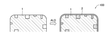
- FIG. 6 is a schematic diagram showing a titanium oxide electrode 201 according to Experimental Example 1.
- FIG. 6 is a schematic diagram showing a titanium oxide electrode 101 according to Experimental Example 1.
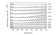
- FIG. 6 is a graph showing water decomposition activity of rutile titanium oxide electrodes 101a to 101i and 201a according to Experimental Example 1.
- FIG. 4 is a graph showing current densities of rutile titanium oxide electrodes 101a to 101i and 201a at a reference voltage of 1.0V.
- 6 is a graph showing water decomposition activity of anatase-type titanium oxide electrodes 101j to 101r and 201b according to Experimental Example 1.
- 6 is a graph showing current densities of anatase-type titanium oxide electrodes 101j to 101r and 201b at a reference voltage of 1.0 V.
- 6 is a schematic diagram showing a tungsten oxide electrode 202 according to Experimental Example 2.
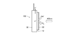
- FIG. 6 is a schematic diagram showing a tungsten oxide electrode 102 according to Experimental Example 2.
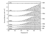
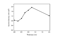
- FIG. 7 is a graph showing water decomposition activity of tungsten oxide electrodes 102a to 102f and 202 according to Experimental Example 2.
- 6 is a graph showing current densities of tungsten oxide electrodes 102a to 102f and 202 at a reference voltage of 1.0V.
- 10 is a graph showing water decomposition activity of tungsten oxide electrodes 102g to 102l and 202 according to Experimental Example 2.
- 6 is a graph showing current densities of tungsten oxide electrodes 102g to 102l and 202 at a reference voltage of 1.0V.
- It is a schematic diagram which shows the anatase type titanium oxide structure 203 which concerns on Experimental example 3.
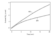
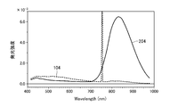
- FIG. 6 is a graph showing organic matter decomposing activities of anatase-type titanium oxide structures 103 and 203 according to Experimental Example 3. It is a figure which shows the emission spectrum of the rutile type titanium oxides 104 and 204 which concern on Experimental example 4. It is a figure explaining time-resolved spectroscopy measurement. It is a figure explaining time-resolved spectroscopy measurement. It is a figure explaining time-resolved spectroscopy measurement. It is a figure explaining time-resolved spectroscopy measurement. 6 is a diagram showing a transient absorption spectrum of rutile titanium oxide 205 according to Experimental Example 5. FIG.
- FIG. 10 is a diagram showing a transient absorption spectrum of rutile titanium oxide 105 according to Experimental Example 5.
- FIG. 6 is a graph showing transient absorption intensity of rutile titanium oxide 105 according to Experimental Example 5. It is a figure which shows the transient absorption spectrum of the anatase type titanium oxide 206 which concerns on Experimental example 6.
- FIG. 10 is a graph showing water decomposition activity of rutile titanium oxide electrodes 107a and 207a according to Experimental Example 7.
- 14 is a graph showing water decomposition activity of anatase-type titanium oxide electrodes 107b and 207b according to Experimental Example 7.
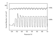
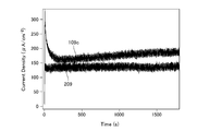
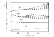
- FIG. 10 is a graph showing water decomposition activity of rutile titanium oxide electrodes 108a to 108c and 208 according to Experimental Example 8.
- 12 is a graph showing water decomposition activity of rutile titanium oxide electrodes 108c and 208 according to Experimental Example 8.
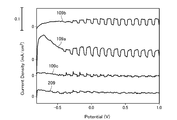
- 10 is a graph showing water decomposition activity of anatase-type titanium oxide electrodes 109a to 109c and 209 according to Experimental Example 9.
- 10 is a graph showing water decomposition activity of anatase-type titanium oxide electrodes 109c and 209 according to Experimental Example 9.
- 10 is a graph showing water decomposition activity when rutile titanium oxide electrodes 108a to 108c and 208 according to Experimental Example 8 are irradiated with visible light.
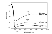
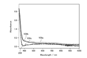
- FIG. 10 is a diagram showing transient absorption spectra of rutile-type titanium oxide electrodes 108a to 108c and 208 according to Experimental Example 8.
- 10 is a graph showing water decomposition activity when anatase-type titanium oxide electrodes 109a to 109c and 209 according to Experimental Example 9 are irradiated with visible light.
- FIG. 10 is a graph showing water decomposition activity of anatase-type titanium oxide electrodes 109c and 209 according to Experimental Example 9.
- 12 is a diagram showing transient absorption spectra of anatase-type titanium oxide electrodes 109a to 109c and 209 according to Experimental Example 9.
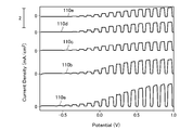
- 12 is a graph showing water decomposition activity of anatase-type titanium oxide electrodes 110a to 110e according to Experimental Example 10.
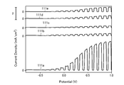
- 14 is a graph showing water decomposition activity of rutile titanium oxide electrodes 111a to 111e according to Experimental Example 11.
- FIG. 1 is a cross-sectional view illustrating a schematic configuration of a structure 100 according to the first embodiment.
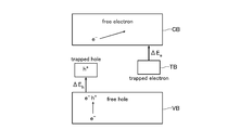
- FIG. 2 is a schematic diagram showing an energy band of the metal compound 1 according to the present embodiment.
- 3 and 4 are schematic views illustrating an example of the structure 100 according to the present embodiment.
- the structure 100 includes a metal compound 1 (first metal compound) and a coating layer 2 (second metal compound layer) disposed on the surface of the metal compound 1. Is provided.
- metal compound 1 one that exhibits photocatalytic activity by irradiation with excitation light (ultraviolet light, visible light, or near infrared light) can be used.
- Metal oxynitrides such as zinc oxide (LaTiO 2 N), metal sulfides such as zinc sulfide (ZnS), cadmium sulfide (CdS), mercury sulfide (HgS), molybdenum sulfide (MoS 2 ), Sm 2 Ti 2 S 2 O
- metal compounds such as metal oxy
- the metal compound 1 is a structure other than an amorphous structure.
- the surface structure of the metal compound 1 is not uniform, and surface defects such as oxygen defects, nitrogen defects, sulfur defects, metal defects, and metal insertion defects exist.
- the metal compound 1 when the metal compound 1 is irradiated with light energy (h ⁇ ) having a band gap or more, the excited electron e ⁇ moves from the valence band VB to the conduction band CB, and then within several picoseconds.
- the trap level TB is trapped by surface defects. When the trap level TB due to this surface defect is deep, the photocatalytic activity of the metal compound 1 falls.
- the electrons trapped in the trap level TB may be referred to as “trap electrons”.
- size of the metal compound 1 which is a metal catalyst It can be set as arbitrary shapes, such as layer shape, particle shape, and column shape.
- a metal compound 1, a quartz glass substrate, FTO glass substrates, various substrates such as CaF 2 substrate, may be provided on the other support.
- the coating layer 2 is a layer deposited so as to fill the surface defects of the metal compound 1. It may be located on the outermost part of the structure 100, and may further include a protective layer on the surface thereof. Various known methods can be employed as the method for depositing the coating layer 2, and it is particularly preferable to deposit using a later-described atomic layer deposition apparatus (Atomic Layer Deposition (ALD) apparatus).
- ALD atomic layer deposition
- the coating layer 2 may be deposited on the entire surface of the metal compound 1 or may be deposited only on a part of the surface of the metal compound 1. Further, the coating layer 2 may be deposited only on the defect of the metal compound 1.
- the coating layer 2 is composed of a metal compound having a structure different from the crystal structure of the metal compound 1 (second structure of the present invention).
- the different structure means a crystal structure different from that of the metal compound 1, an amorphous structure, or a mixed structure of crystal and amorphous.
- the structure of the coating layer 2 include an anatase type and a rutile type in the case of a crystal structure.
- the structure of the coating layer 2 a structure that can suppress structural distortion caused by surface defects of the metal compound 1 and has few defects is preferable. From this viewpoint, the coating layer 2 is most preferably an amorphous structure. In this case, the amorphous structure may partially include a rutile type and / or anatase type crystal structure.
- an anatase type is preferable to a rutile type.
- the same compound as the metal compound 1 can be used.
- the valence of the metal cation of the coating layer 2 is preferably the same as or smaller than the valence of the metal cation of the metal compound 1.
- the metal compound 1 is titanium oxide
- the metal cation of the coating layer 2 is Ti 4+ , Si 4+ , Zr 4+ , Ga 3+ , Al 3+ , Zn 2+, etc.
- Cr 6+ and W 6+ are not preferable. This is because the coating layer 2 itself tends to attract and capture electrons as the valence increases.
- the thickness of the coating layer 2 is not particularly limited, but is usually 20 nm or less, preferably 0.1 nm to 10 nm, more preferably 0.2 nm to 7 nm. If the thickness of the coating layer 2 is 20 nm or less, the light absorbed by the coating layer 2 is small, and the movement of the excited electrons of the metal compound 1 is difficult to be inhibited. can do. In addition, when it is smaller than 0.1 nm or larger than 10 nm, it is difficult to improve the photocatalytic activity. In the present embodiment, the coating layer 2 is made of the same metal compound as the metal compound 1, but has a photocatalytic activity or becomes low due to the thickness being 0.1 nm to 10 nm.
- FIG. 3 shows an example in which the metal compound 1 is a rutile type or anatase type titanium oxide and the coating layer 2 is an amorphous titanium oxide.
- FIG. 4 shows an example in which the metal compound 1 is a rutile type or anatase type titanium oxide and the coating layer 2 is an amorphous gallium oxide and an amorphous tantalum oxide.
- the coating layer 2 disposed on the surface of the metal compound 1 can be a metal compound having a crystal structure different from that of the metal compound 1 and having the same or different composition as the metal compound 1.
- a composite metal compound having two or more metal elements can be formed as the coating layer 2 using a plurality of metal compounds having different compositions. 3 and 4, the crystal structures (atom arrangement) of the metal compound 1 and the coating layer 2 are schematically shown, and may be different from actual ones.
- a protective layer (not shown) may be provided on the surface of the coating layer 2.
- the protective layer is a layer intended to protect the surface of the coating layer 2 and contributes to an improvement in photocatalytic activity and an increase in durability.
- Examples of the compound constituting the protective layer include aluminum oxide, zirconium oxide (ZrO 2 ), and silicon dioxide (silica).
- the protective layer is composed of a compound having a structure (third structure) different from the crystal structure of the metal compound 1.
- the structure of the protective layer and the structure of the coating layer 2 may be the same or different from each other.
- the structure of the protective layer is most preferably an amorphous structure.
- the thickness of the protective layer is usually 5 nm or less, and preferably in the range of 0.1 to 3 nm.
- the protective layer may be provided on the entire surface of the coating layer 2 or may be provided on a part of the surface. Further, when the coating layer 2 is provided on a part of the surface of the metal compound 1, a protective layer may also be disposed on the surface of the metal compound 1.
- Structure of the present invention 100 (a first metal compound having a second metal compound layer on the surface), in resolved spectroscopy measurement time measured after 5 ⁇ s laser pulse irradiation, 1000 cm -1 or 20000 cm -1 following wavenumber range the maximum value of the transient absorption intensity at the inner is present in the wave number range of 1000 cm -1 or 8000 cm -1 or less, the ratio of the transient absorption intensity of this maximum value for the transient absorption intensity at a wave number 15000 cm -1 is 10 times or more.
- the maximum value of the transient absorption intensity is the value of the transient absorption intensity at the position showing the absorption peak of the transient absorption intensity as shown in FIG. 18 described later, and does not show the absorption peak as shown in FIG. 21 described later. Is the value of the transient absorption intensity at the position where absorption is exhibited.
- the free electrons (Free e ⁇ ) of the metal compound 1 contribute to the photocatalytic activity, and the photocatalytic activity increases as the number increases.
- the metal compound 1 that does not include the coating layer 2 on the surface has a surface defect, and this surface defect causes a distortion in the charge balance of the metal compound 1 and the like.
- the metal compound 1 contains many electrons (trapped e ⁇ ) and holes (trapped h + ) trapped in deep defect levels. The electrons excited by the light irradiation are trapped by the trapped electrons and holes, and as a result, the photocatalytic activity decreases.
- the covering layer 2 may have any structure as long as it has a structure that reduces the strain of the metal compound 1. However, since the strain cannot be reduced in the case of the same crystal structure as the metal compound 1, the structure is different from that of the metal compound 1. Need to be.
- the free electrons (Free e -) is to provide a strong absorption from the mid-infrared to the microwave region, the absorption intensity as wave number toward the 0 cm -1 is higher in the transient absorption spectra by time-resolved spectroscopy, 0 cm - 1 has an absorption peak (see FIG. 15 described later).
- electrons (trapped e ⁇ ) and holes (trapped h + ) trapped in deep defect levels absorb in the visible light to near infrared region. Therefore, when the trap level TB for trapping electrons becomes shallower, the absorption wavelength given by the trapped electrons shifts to the longer wavelength side.
- the absorption intensity of wave numbers from 10000 cm ⁇ 1 to 15000 cm ⁇ 1 Becomes higher. Therefore, the behavior of free electrons, trapped electrons, and holes can be independently evaluated by measuring the transient absorption spectrum by time-resolved spectroscopy.
- Structure 100 of the present invention for example as shown in FIG. 18, has an absorption peak in a wave number range 1000 cm -1 or 8000 cm -1, transient absorption intensity at the absorption peak wavenumber 1000 cm -1 or more 20000 cm - The maximum value of transient absorption intensity within a range of 1 or less is shown.
- the provision of the coating layer 2 means that the surface defects of the metal compound 1 are filled, and the defect levels of the trapped electrons and holes are shallow. As a result, the number of excited electrons trapped by the surface defects is reduced, and the photocatalytic activity is improved.
- the wave number indicating the maximum transient absorption intensity is in the vicinity of 0 cm ⁇ 1 .
- the above mechanism is not limited to a specific photocatalytic compound such as titanium oxide or tungsten oxide, but also applies to various other photocatalytic compounds.
- the ratio of the maximum value to the transient absorption intensity at a wave number of 15000 cm ⁇ 1 is 10 times or more, preferably 15 times or more, and preferably 30 times or more. It is more preferable that the ratio is 100 times or more.
- the above maximum value is 10 times or more with respect to the transient absorption intensity at the wave number of 15000 cm ⁇ 1 , the number of free electrons and the number of electrons trapped in the shallow defect level are sufficiently large, and the photocatalytic activity is increased. It can be said that.
- the metal compound 1 according to the present embodiment has an absorption peak in a wave number range of a first wave number (for example, 7000 cm ⁇ 1 ) or more in a transient absorption spectrum by time-resolved spectroscopic measurement. Further, the structure 100 having the coating layer 2 on the surface of the metal compound 1 has an absorption peak in a wave number range less than the first wave number (for example, 7000 cm ⁇ 1 ) in a transient absorption spectrum by time-resolved spectroscopic measurement. As described above, the transient absorption spectrum of the structure 100 has an absorption peak on the lower wave number side than the transient absorption spectrum of the metal compound 1 alone. In addition, the transient absorption spectrum of the structure 100 has a higher absorption intensity on the low wave number side than the transient absorption spectrum of the metal compound 1.
- the trap level of a metal compound used as a photocatalyst can be estimated from the position of the emission peak due to recombination of carriers trapped in the trap by measuring the emission spectrum.
- the emission peak appearing on the long wavelength side of 700 nm or more is derived from trapped electrons that have fallen into a deep trap level.
- the emission peak appearing on the short wavelength side of less than 700 nm is derived from trapped electrons or free electrons that have fallen into a shallow trap level.
- the metal compound 1 has an emission peak in a first wavelength region (for example, a wavelength region of 700 nm or more) longer than the first wavelength (for example, 700 nm) in an emission spectrum when excited by excitation light.
- the structure 100 of the present invention has a second wavelength band shorter than the first wavelength (for example, 700 nm) (for example, a wavelength band of less than 700 nm) in the emission spectrum when excited by excitation light.
- the metal compound 1 is rutile titanium oxide 204
- the rutile titanium oxide 204 has an emission peak at 840 nm in an emission spectrum when excited by excitation light.
- the structure 104 having an amorphous titanium oxide layer on the surface of rutile titanium oxide has an emission peak at 500 nm.
- the structure 100 having the coating layer 2 on the surface of the metal compound 1 has a light emission intensity in the second wavelength region that is higher than the light emission intensity of the metal compound 1.
- the emission spectrum of the structure 100 has an emission peak in a wavelength region (second wavelength region) shorter than the first wavelength, compared to the emission spectrum of the metal compound 1 alone.
- the light emission intensity of the structure 100 is larger in the wavelength region (second wavelength region) on the shorter wavelength side than the first wavelength, compared to the light emission intensity of the metal compound 1.
- the structure 104 having an amorphous titanium oxide layer on the surface has higher emission intensity than the rutile titanium oxide 204 in a wavelength region of less than 700 nm.
- the structure 100 according to this embodiment can be used as a photocatalyst material for various applications in various fields.
- a photocatalyst electrode a metal oxide thin film transparent electrode, a dye-sensitized solar cell, a perovskite solar cell, an anti-fogging / anti-proofing agent. It can be applied to soiling materials and antibacterial materials.
- the manufacturing method of the structure 100 according to the present embodiment uses an atomic layer deposition apparatus (ALD apparatus) on the surface of the metal compound 1 having surface defects to have a thickness of 0.1 nm to It has the process of forming the coating layer 2 so that it may become 10 nm.
- ALD apparatus atomic layer deposition apparatus
- the atomic layer deposition apparatus is suitable for forming a very thin film because it enables film formation for each atomic layer.
- the atomic layer deposition method (ALD method) is a method in which two or more kinds of gaseous raw materials are alternately supplied to a reaction chamber to cause a chemical reaction on the film formation surface, which is equivalent to an atomic layer in one cycle.
- the thickness of the level can be formed with high accuracy.
- a known apparatus can be used as the atomic layer deposition apparatus.
- the formation of the coating layer 2 by the atomic layer deposition apparatus is preferably performed under conditions of 80 ° C. to 400 ° C., more preferably 80 ° C. to 300 ° C.
- the structure of the coating layer 2 can be changed depending on the temperature at which the coating layer 2 is formed. For example, when the coating layer 2 is made of titanium oxide, an amorphous structure is formed if the formation temperature of the coating layer 2 is 300 ° C. or lower, and if it exceeds this, anatase type crystal structure is mixed in part.
- the crystal structure is as follows.
- a metal compound 1 may have a step of fixing the FTO glass substrate or CaF 2 on a variety of supports such as a substrate.
- the method for fixing the metal compound 1 on the support is not particularly limited, and any method such as a method of applying and sintering the powder of the metal compound 1 can be employed.
- the process of carrying out UV (ultraviolet) ozone treatment on the surface of the metal compound 1 as pretreatment.
- the conditions for the UV ozone treatment are not particularly limited, but the flow rate of supplied oxygen is preferably 1 to 10 ml / min.
- the treatment time is preferably 3 to 20 minutes.
- the wavelength range of the irradiated UV is preferably 185 nm to 254 nm, the output is preferably 20 to 45 W, and the irradiation intensity is preferably 2000 to 3500 ⁇ W / cm 2 .
- an annealing treatment step may be performed as necessary.
- the annealing conditions are not particularly limited, but the heating temperature is preferably 100 ° C. to 800 ° C., more preferably 100 ° C. to 500 ° C.
- the heating time is preferably 0.25 to 1.5 hours, more preferably 0.5 to 1 hour.
- the annealing method is not particularly limited, and a known oven or the like can be used.
- the photocatalytic activity may be reduced by performing the annealing process as compared with the case where the annealing process is not performed. This is considered to be because the structure of the coating layer 2 is changed by performing the annealing process, and may have a structure similar to the crystal structure of the metal compound 1. For example, when the structure of the coating layer 2 is an amorphous structure, crystallization is promoted by annealing treatment, and the same crystal structure as that of the metal compound 1 may be changed.
- FIG. 5A is a schematic diagram showing a titanium oxide electrode 201 according to a conventional example.
- FIG. 5B is a schematic diagram showing a titanium oxide electrode 101 having a coating layer 21 on the surface.
- the titanium oxide electrode 201 according to the conventional example is an electrode having the titanium oxide layer 11 on the FTO glass substrate 31, but does not have the coating layer 21.
- a layer in which the titanium oxide layer 11 is a rutile type titanium oxide layer is referred to as a rutile type titanium oxide electrode 201a
- a case in which the titanium oxide layer is an anatase type titanium oxide layer is referred to as an anatase type titanium oxide electrode 201b.
- the titanium oxide electrode 101 according to the present invention has an amorphous titanium oxide layer 21 as a coating layer on the surface of the titanium oxide layer 11 (first metal compound) of the titanium oxide electrode 201 shown in FIG. 5A. It is an electrode obtained by forming (second metal compound layer). An amorphous titanium oxide layer 21 as a second metal compound layer is formed on the titanium oxide layer 11 under a temperature condition of 100 ° C. using an electronic layer deposition apparatus (Cambridge Nanotech, Savannah G2, S100), and a coating layer A titanium oxide electrode 101 having 21 was obtained.
- an amorphous titanium oxide layer 21 having a thickness of 1 nm, 2 nm, 3 nm, 4 nm, 5 nm, 6 nm, 7 nm, 10 nm, or 20 nm is formed on the surface of the rutile type titanium oxide electrode 201a, and the rutile type titanium oxide electrode 101a ⁇ 101i.
- an amorphous titanium oxide layer 21 having a thickness of 1 nm, 2 nm, 3 nm, 4 nm, 5 nm, 6 nm, 7 nm, 10 nm, or 20 nm is formed on the surface of the anatase type titanium oxide electrode 201b, respectively, and the anatase type titanium oxide electrodes 101j to 101r are formed. It was.
- a silver / silver chloride electrode is used as a reference electrode
- a 0.1 M Na 2 SO 4 aqueous solution is used as an electrolyte
- an LED lamp M375L3, manufactured by Thorlabs
- Water was decomposed by intermittently irradiating 375 nm ultraviolet rays at 0.1 Hz (200 mW / cm 2 ), and the current density was measured to evaluate the water decomposition activity.
- the current density was measured using a potentio galvanostat (PS-14, manufactured by Toho Giken Co., Ltd.) while changing the applied potential from ⁇ 0.5 V to 1.0 V with respect to the reference electrode at a rate of 10 mV / s. This was done by measuring the oxidation current due to the oxidation of water.
- PS-14 potentio galvanostat
- FIG. 6A is a graph showing the water decomposition activity of the titanium oxide electrodes 101a to 101i and 201a in which the titanium oxide layer 11 is a rutile type.
- FIG. 6B is a graph showing the current density of rutile titanium oxide electrodes 101a to 101i and 201a at a reference voltage of 1.0V.
- FIG. 7A is a graph showing the water decomposition activity of the titanium oxide electrodes 101j to 101r and 201b in which the titanium oxide layer 11 is of anatase type.
- FIG. 7B is a graph showing current densities of anatase titanium oxide electrodes 101j to 101r and 201b at a reference voltage of 1.0V.
- FIGS. 1 is a graph showing the water decomposition activity of the titanium oxide electrodes 101a to 101i and 201a in which the titanium oxide layer 11 is a rutile type.
- FIG. 6B is a graph showing the current density of rutile titanium oxide electrodes 101a to 101i and
- Table 1 shows current densities of rutile titanium oxide electrodes 101a to 101i and 201a at a reference voltage of 1.0 V
- Table 2 shows current densities of anatase titanium oxide electrodes 101j to 101r and 201b at a reference voltage of 1.0 V. Indicated.
- the current density generated by the decomposition of water by the rutile-type titanium oxide electrode 201a not having the coating layer 21 is a reference voltage of 1.0 V and 0.2 mA / cm 2 at the time of ultraviolet irradiation. is there.
- the current density generated by the decomposition of water by the rutile titanium oxide electrodes 101a ⁇ 101h having a coating layer 21 is a 0.4mA / cm 2 ⁇ 13mA / cm 2 , respectively, in the reference voltage 1.0 V.
- the current density generated by the decomposition of water by the rutile titanium oxide electrode 101i having a thickness of the coating layer 21 of 20 nm is 0.02 mA / cm 2 at a reference voltage of 1.0 V.
- the water decomposition activity of the rutile-type titanium oxide electrode increases as the thickness of the amorphous titanium oxide layer 21 increases from 1 nm to 5 nm, and is 5 nm (rutile-type titanium oxide). It can be seen that the maximum is obtained at the electrode 101e).
- the current density generated by the decomposition of water by the anatase-type titanium oxide electrode 201b not having the coating layer 21 is 0.2 mA / cm 2 at the reference voltage of 1.0 V.
- the current density generated by the decomposition of water by the anatase titanium oxide electrode 101j ⁇ 101 q having a coating layer 21 is a 0.5mA / cm 2 ⁇ 6.5mA / cm 2 , respectively, in the reference voltage 1.0 V.
- the current density generated by the decomposition of water by the anatase-type titanium oxide electrode 101r having a thickness of the covering layer 21 is 0.3 mA / cm 2 at a reference voltage of 1.0 V. As shown in FIG.
- the water decomposition activity of the anatase-type titanium oxide electrode increases as the thickness of the amorphous titanium oxide layer 21 increases from 1 nm to 5 nm and is 5 nm (anatase-type titanium oxide). It can be seen that it is maximum at electrode 101n) and then decreases as the thickness increases.
- the rutile-type titanium oxide electrodes 101a to 101h and the anatase-type titanium oxide electrodes 101j to 101q having the coating layer 21 having a thickness of 1 nm to 10 nm have the titanium oxide electrodes 201a and 201b and the coating layer 21 having a thickness of 20 nm. It can be seen that the current density generated by the decomposition of water is larger than that of the titanium oxide electrodes 101i and 101r.
- FIG. 8A is a schematic diagram showing a tungsten oxide electrode 202 according to a conventional example.
- FIG. 8B is a schematic diagram showing a tungsten oxide electrode 102 having a coating layer 22 on the surface.
- the tungsten oxide electrode 202 according to the conventional example has the tungsten oxide layer 12 on the FTO glass substrate 32 but does not have the coating layer 22.
- a coating layer 22 (second metal compound layer) is formed on the surface of the tungsten oxide layer 12 (first metal compound) of the conventional tungsten oxide electrode 202 shown in FIG. 8A. Electrode.
- the coating layer 22 is formed on the tungsten oxide layer 12 under a temperature condition of 100 ° C. using an electronic layer deposition apparatus (ALD) (Cambridge Nanotech, Savannah G2, S100) to obtain a tungsten electrode 102 having a coating layer. It was.
- ALD electronic layer deposition apparatus
- amorphous titanium oxide having a thickness of 0.2 nm, 0.4 nm, 0.6 nm, 0.8 nm, 1 nm, or 2 nm is formed as the covering layer 22, respectively. 102a to 102f.
- amorphous tantalum oxide having a thickness of 0.2 nm, 0.4 nm, 0.6 nm, 0.8 nm, 1 nm, or 2 nm is formed as a coating layer 22 on the surface of the tungsten oxide electrode 202, and the tungsten oxide electrodes 102g to 102l are formed. It was.
- the current density was measured using a potentio galvanostat (PS-14, manufactured by Toho Giken Co., Ltd.) while changing the applied potential from 0.5 V to 1.0 V at a rate of 10 mV / s with respect to the reference electrode. This was done by measuring the oxidation current due to the oxidation of.
- PS-14 potentio galvanostat
- FIG. 9A is a graph showing the water decomposition activity when the coating layer 22 is amorphous titanium oxide.
- FIG. 9B is a graph showing the current density of the tungsten oxide electrodes 102a to 102f and 202 at a reference voltage of 1.0V.
- FIG. 10A is a graph showing the water decomposition activity when the coating layer 22 is amorphous tantalum oxide.
- FIG. 10B is a graph showing the current density of the tungsten oxide electrodes 102g to 102l and 202 at the reference voltage of 1.0V.
- the baseline is shifted to clarify the difference in water decomposition activity.
- the current density generated by the decomposition of water by the tungsten oxide electrode 202 without the coating layer 22 is 0.85 mA / cm 2 at a reference voltage of 1.0 V.
- the current density generated by the decomposition of water by the tungsten oxide electrodes 102b to 102e is 1.5 mA / cm 2 to 3.8 mA / cm 2 at a reference voltage of 1.0 V.
- tungsten oxide electrodes 102b to 102e each having an amorphous titanium oxide layer having a thickness of 0.4 nm to 1 nm as a covering layer 22 are a tungsten oxide electrode 202, an amorphous titanium oxide layer having a thickness of 0.2 nm, and 2 nm. It can be seen that the current density generated by the decomposition of water is larger than that of the tungsten oxide electrodes 102a and 102f having the thickness.
- the water decomposition activity of the tungsten oxide electrode increases as the thickness of the amorphous titanium oxide layer as the coating layer 22 increases from 0.2 nm to 1 nm, and increases to 1 nm (tungsten oxide electrode 102e). It turns out that it becomes the maximum in the case.
- tungsten oxide electrodes 102h to 102l having an amorphous tantalum oxide layer with a thickness of 0.4 nm to 2 nm are oxidized with a tungsten oxide electrode 202 and an amorphous tantalum oxide layer with a thickness of 0.2 nm. It can be seen that the current density generated by the decomposition of water is larger than that of the tungsten electrode 102g.
- the water decomposition activity of the tungsten oxide electrode increases as the thickness of the amorphous tantalum oxide layer as the coating layer 22 increases from 0.2 nm to 1 nm, and increases to 1 nm (tungsten oxide electrode 102k). It turns out that it becomes the maximum in the case.
- FIG. 11A is a schematic diagram showing an anatase-type titanium oxide structure 203 according to a conventional example.
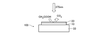
- FIG. 11B is a schematic diagram showing an anatase-type titanium oxide structure 103 having an amorphous titanium oxide layer 23 on the surface.
- FIG. 12 is a graph showing the relationship between acetic acid decomposition time and carbon dioxide production in anatase-type titanium oxide structures 103 and 203.
- Anatase-type titanium oxide structure 203 shown in FIG. 11A forms anatase-type titanium oxide thin film 23 by applying 20 mg of anatase-type titanium oxide particles on a 5 cm 2 FTO glass substrate 33 and fixing and sintering them. can get.
- An anatase-type titanium oxide structure 103 shown in FIG. 11B is formed on an anatase-type titanium oxide thin film 13 (first metal compound) shown in FIG. 11A on an electronic layer deposition apparatus (ALD) (manufactured by Cambridge Nanotech, Savannah G2 S100). )
- ALD electronic layer deposition apparatus
- Each of the anatase-type titanium oxide structures 103 and 203 was placed in a reaction vessel made of hard glass having a volume of 100 ml, and 10 mg (about 16.7 ⁇ mol) of acetic acid was sufficiently vaporized in the atmosphere.
- An LED lamp manufactured by Thorlabs, M375L3
- An LED lamp was continuously irradiated with ultraviolet rays of 375 nm (200 mW / cm 2 ) to decompose acetic acid, and the amount of carbon dioxide produced was measured.
- the amount of carbon dioxide produced was measured using a micro GC (manufactured by Agilent Technologies, 490-GC). The results are shown in FIG.
- a plot indicated by a circle indicates the amount of carbon dioxide produced by the decomposition of acetic acid by the anatase-type titanium oxide structure 103
- a plot indicated by a square indicates the result by the anatase-type titanium oxide structure 203.
- the amount of carbon dioxide produced by the decomposition of acetic acid is shown.
- the amount of carbon dioxide generated by the decomposition of acetic acid by the anatase-type titanium oxide structure 103 is about 3 ⁇ mol after 15 minutes from the start of the decomposition, which is about the amount of the anatase-type titanium oxide structure 203. 2 times.
- the anatase-type titanium oxide structure 103 having the amorphous titanium oxide layer 23 has a higher acetic acid decomposition rate than the anatase-type titanium oxide structure 203.
- the trap level of the metal compound used as the photocatalyst can be estimated from the position of the emission peak due to the recombination of the carriers trapped in the trap by measuring the emission spectrum.
- the emission peak appearing on the long wavelength side of 700 nm or more is derived from trapped electrons that have fallen into a deep trap level.
- the emission peak appearing on the short wavelength side of less than 700 nm is derived from trapped electrons or free electrons that have fallen into a shallow trap level. Therefore, it can be said that the photocatalytic activity is high when the emission peak in the emission spectrum measurement is in a wavelength region of less than 700 nm.
- the example which evaluated the photocatalytic activity of the structure which concerns on Experimental example 4 by the emission spectrum is demonstrated.
- illustration is omitted, as a conventional example, 3 mg of powdery rutile type titanium oxide was applied to a 1.5 cm 2 CaF 2 substrate to prepare rutile type titanium oxide 204 (first metal compound).
- rutile type titanium oxide 204 having a coating layer formed by forming an amorphous titanium oxide layer (second metal compound layer) having a thickness of 2 nm under a temperature condition of 100 ° C. using an atomic layer deposition apparatus.
- Type titanium oxide 104 was prepared.
- the rutile titanium oxides 104 and 204 were excited by irradiating them with ultraviolet light of 375 nm in the atmosphere at room temperature using a semiconductor laser (Topica Photonics, iBeam smart: 5 mW, beam diameter: 3 mm). Manufactured, SP2300) and a CCD detector (manufactured by Princeton Instruments, PIXIS: 100F), and the emission spectrum was measured with an exposure time of 15 seconds. The results are shown in FIG.
- FIG. 13 shows the emission spectra of rutile titanium oxides 104 and 204.
- FIG. 13 the emission spectrum of rutile titanium oxide 204 is indicated by a solid line, and the emission spectrum of rutile titanium oxide 104 is indicated by a dotted line.
- the broad emission peak centered at 840 nm disappears, the emission intensity around 450 to 700 nm increases, A broad emission band was observed.
- the rutile type titanium oxide 104 having an amorphous titanium oxide layer is larger than the rutile type titanium oxide 204. Note that the emission peak observed near 750 nm is the one where 375 nm ultraviolet light from the semiconductor laser was detected as noise (second harmonic).
- the second metal compound layer having a different structure is formed on the surface of the first metal compound so as to cover the surface defects, thereby increasing trapped electrons or free electrons that have fallen into the shallow trap level. I was able to. In Experimental Examples 1 to 3, it can be seen that this is the reason why the photocatalytic activity is improved when the coating layer is formed.
- FIG. 14 is a schematic diagram showing the energy levels of electrons of a certain metal compound.
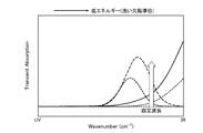
- 15 and 16 are diagrams for explaining the meaning of each peak of the transient absorption spectrum in a certain metal compound.
- the defect structure that captures photoexcited electrons and holes changes, and the depth of the defect level becomes shallow, so that the reaction between electrons and holes occurs.
- the photocatalytic activity is improved because the property is improved.
- the band gap may be excited with a pulse laser, and transient absorption in the visible light to far infrared region or microwave region may be measured.
- free electrons (Free e ⁇ ) in the conduction band CB give strong absorption from the mid-infrared region to the microwave region.
- electrons (trapped e ⁇ ) and holes (trapped h + ) trapped in deep defect levels absorb in the visible light to near infrared region. Therefore, when the trap level TB for trapping electrons becomes shallower, the absorption wavelength given by the trapped electrons shifts to the longer wavelength side.
- the photocatalytic activity can be evaluated by measuring a transient absorption spectrum and observing a change in absorption wavelength or a change in absorption intensity at a fixed wavelength.
- rutile type titanium oxide structure 205 3 mg was applied on a 1.5 cm 2 CaF 2 substrate to form a thin film, thereby obtaining a rutile type titanium oxide structure 205 according to a conventional example. Further, an amorphous titanium oxide layer (second metal compound layer) having a thickness of 2 nm is deposited on the surface of rutile-type titanium oxide 205 (first metal compound) at a temperature of 100 ° C. by an atomic layer deposition apparatus (Cambridge Nanotech). The rutile type titanium oxide structure 105 according to the present invention was obtained by Savannah G2 S100).
- the rutile titanium oxide structures 105 and 205 are irradiated with a laser pulse of 355 nm (Continuum, Surelite I: intensity 0.5 mJ) in vacuum at 6 ns and 5 Hz to excite the band gap, and time-resolved spectroscopy was carried out to obtain the transient absorption spectra of the visible light-far-infrared region, the microwave region (wavenumber range of 25000cm -1 ⁇ 1000cm -1).
- Time-resolved spectrometry, known devices, was carried out by the method (Akira Yamakata, Junie Jhon M. Vequizo , and Hironori Matsunaga (2015). Distinctive Behavior of Photogenerated Electrons and Holes in Anatase and Rutile TiO 2 Powders, J. Phys. Chem. C 119, 24538-24545). The results are shown in FIGS.
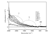
- FIG. 17 is a diagram showing a transient absorption spectrum in the time-resolved spectroscopic measurement of the rutile-type titanium oxide structure 205.
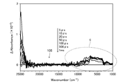
- FIG. 18 is a diagram showing a transient absorption spectrum in the time-resolved spectroscopic measurement of the rutile-type titanium oxide structure 105.
- Figure 19 is a graph showing the absorption intensity at a wave number 2000 cm -1 and 6000 cm -1, the relationship between the thickness of the amorphous titanium oxide layer of rutile titanium oxide structure 105.
- the rutile-type titanium oxide structure 205 has an absorption peak a due to holes and a transient absorption peak b due to trapped electrons in a wave number range larger than the wave number 8000 cm ⁇ 1 .
- rutile-type titanium oxide structure 105 having an amorphous titanium oxide layer on the surface as shown in FIG. 18, the wave number 1000 cm -1 or 8000 cm -1
- the following wavenumber range, transient absorption peak due to highly reactive electron c It can be seen that the peak position is shifted to the long wavelength side as compared with the case of only rutile titanium oxide. From this, it can be seen that by forming the amorphous titanium oxide layer, the electron trap level becomes shallow and the photocatalytic activity is improved.
- the transient absorption intensity at a wave number of 2000 cm ⁇ 1 is maximized when the thickness of the amorphous titanium oxide layer is 10 nm. It can also be seen that the transient absorption intensity at a wave number of 6000 cm ⁇ 1 is maximized when the thickness of the amorphous titanium oxide layer is 3 nm.
- the rutile-type titanium oxide structure 105 has an absorption peak at a wave number of 6600 cm ⁇ 1 when measured 5 ⁇ s after laser pulse irradiation in time-resolved spectroscopy, and the absorption peak has a wave number of 1000 cm ⁇
- the maximum value of transient absorption intensity in the wave number range of 1 to 20000 cm ⁇ 1 is shown.
- the rutile-type titanium oxide structure 105 provided with a coating layer of amorphous titanium oxide has a transient absorption intensity at an absorption peak (wave number 6600 cm ⁇ 1 ) of about 110 with respect to the transient absorption intensity at a wave number 15000 cm ⁇ 1 . It turns out that it is double. Furthermore, rutile titanium oxide structure 105, transient absorption intensity at wave number 1000 cm -1 is found to be approximately 31 times the transient absorption intensity at a wavenumber 15000 cm -1.
- rutile type titanium oxide 105 can be said to have high photocatalytic activity because the ratio of the transient absorption intensity at wave number 15000 cm ⁇ 1 to the transient absorption intensity at the absorption peak (wave number 6600 cm ⁇ 1 ) is 10 times or more.
- rutile-type titanium oxide structure 205 according to the related art having no coating layer, as shown in FIG. 17, the wave number 1000 cm -1 or 8000 cm -1 The following wavenumber ranges, having an absorption peak at a wavenumber of 5800cm -1 . Furthermore, rutile titanium oxide structure 205, the wave number 1000 cm -1 or 20000 cm -1 or less wavenumber range, with a maximum of the transient absorption intensity at a wavenumber of 20000 cm -1.
- the rutile type titanium oxide structure 205 shows that the transient absorption intensity at the absorption peak (wave number 5800 cm ⁇ 1 ) is about 0.43 times the transient absorption intensity at the wave number 15000 cm ⁇ 1 . .
- the ratio of the transient absorption intensity at the wave number of 15000 cm ⁇ 1 to the transient absorption intensity at the absorption peak (wave number of 5800 cm ⁇ 1 ) is less than 10 times, the rutile-type titanium oxide structure 205 has a low photocatalytic activity. I can say that.
- an anatase-type titanium oxide thin film was formed on a CaF 2 substrate to obtain an anatase-type titanium oxide structure 206 according to a conventional example. Further, an amorphous titanium oxide layer (second metal compound layer) having a thickness of 2 nm is formed on the surface of the anatase-type titanium oxide structure 206 (first metal compound) under a temperature condition of 100 ° C. by an atomic layer deposition apparatus. The anatase-type titanium oxide structure 106 according to the present invention was obtained. The anatase-type titanium oxide structures 106 and 206 were subjected to time-resolved spectroscopic measurement in the same manner as in Experimental Example 5 to obtain transient absorption spectra.
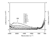
- FIG. 20 is a diagram showing a transient absorption spectrum in the time-resolved spectroscopic measurement of the anatase type titanium oxide structure 206.
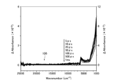
- FIG. 21 is a diagram showing a transient absorption spectrum in the time-resolved spectroscopic measurement of the anatase-type titanium oxide structure 106.
- the transient absorption intensity in the wave number range below 6000 cm ⁇ 1 refers to the right vertical axis.
- the transient absorption intensity in the wave number range below 5800 cm ⁇ 1 refers to the right vertical axis.
- the anatase type titanium oxide structure 206 has a transient absorption peak due to free electrons or shallow trapped electrons at a wave number of 5800 cm ⁇ 1 .
- the anatase-type titanium oxide structure 106 of the present invention having an amorphous titanium oxide layer on the surface has no change in the position of the absorption peak as compared with the anatase-type titanium oxide structure 206. It can be seen that the absorption intensity is increased. Therefore, it can be seen that the number of electrons having high reaction activity increases by forming an amorphous titanium oxide layer on the surface of anatase-type titanium oxide.
- anatase type titanium oxide structure 106 comprising a coating layer of amorphous titanium oxide, time-resolved spectroscopic measurement when measured after 5 ⁇ s laser pulse irradiation at wave number 1000 cm -1 or 20000 cm -1 following wavenumbers In the range, the maximum value of the transient absorption intensity is at a wave number of 1000 cm ⁇ 1 .
- the anatase-type titanium oxide structure 106 has an absorption peak at a wave number of 5800 cm ⁇ 1 .
- the anatase-type titanium oxide structure 106 has a transient absorption intensity at the absorption peak (wave number 5800 cm ⁇ 1 ) that is about 25 times the transient absorption intensity at the wave number 15000 cm ⁇ 1 .
- the ratio of the transient absorption intensity at the wave number of 15000 cm ⁇ 1 to the transient absorption intensity at the absorption peak (wave number of 5800 cm ⁇ 1 ) of the anatase type titanium oxide structure 106 is 10 times or more, the photocatalytic activity is high. I can say that.
- anatase titanium oxide structure 106 transient absorption intensity at wave number 1000 cm -1 transient absorption intensity is maximum, it can be seen that about 150 times the transient absorption intensity at a wavenumber 15000 cm -1. From this, it can be said that the anatase-type titanium oxide structure 106 has a large number of free electrons and high photocatalytic activity.
- the anatase type titanium oxide structure 206 having no coating layer as shown in FIG. 20, the wave number 1000 cm -1 or 8000 cm -1
- the anatase titanium oxide structure 206, and transient absorption intensity in the laser pulse irradiation of 5 ⁇ s after wavenumber 20000 cm -1 as measured in, 5800cm -1, 2000cm -1, 1000cm -1 in time-resolved spectroscopy, wavenumber Table 6 shows the ratio to the transient absorption intensity at 15000 cm ⁇ 1 .
- anatase titanium oxide structure 206 transient absorption intensity at the absorption peak (wavenumber 6000 cm -1) is found to be about 1.1 times the transient absorption intensity at a wavenumber 15000 cm -1 .
- the photocatalytic activity is low I can say that.
- transient absorption intensity at wave number 1000 cm -1 is found to be about 5.0 times the transient absorption intensity at a wavenumber 15000 cm -1. From this, it can be said that the anatase-type titanium oxide structure 206 has a small number of free electrons and a low photocatalytic activity.
- the manufacturing method of the structure based on a comparative example is demonstrated.
- the method for manufacturing the structure according to the comparative example is different from the method for manufacturing the structure 100 according to the first embodiment in the method for forming the coating layer.
- the covering layer 2 is formed using an atomic layer deposition apparatus, whereas in the structure according to the comparative example, the covering layer is formed by a sol-gel method.
- Example 7 (Formation of coating layer by sol-gel method) Rutile titanium oxide and anatase titanium oxide were fixed on an FTO glass substrate to obtain a rutile titanium oxide electrode 207a and an anatase titanium oxide electrode 207b.
- 100 mL of a 200 g / L isopropyl alcohol dispersion was prepared in terms of titanium oxide concentration.
- 10 g / L of titanium tetraisopropoxide / isopropyl alcohol dispersion in terms of titanium oxide concentration was prepared, added to the previous isopropyl alcohol dispersion of titanium oxide, and stirred for 2 hours.
- the solvent was evaporated to obtain a rutile-type titanium oxide electrode 107a and anatase-type titanium oxide electrode 107b which were subjected to amorphous surface treatment.
- the thicknesses of the coating layers in the amorphous surface-treated titanium oxide electrodes 107a and 107b thus obtained were 90 nm and 50 nm, respectively.
- FIG. 22 is a graph showing the water decomposition activity in the amorphous surface-treated rutile titanium oxide 107a
- FIG. 23 is a graph showing the water decomposition activity in the amorphous surface-treated anatase titanium oxide 107b.
- the water decomposition activity of the titanium oxide electrodes 207a and 207b not subjected to the amorphous surface treatment is indicated by a solid line
- the water decomposition activity of the titanium oxide electrodes 107a and 107b subjected to the amorphous surface treatment is indicated by a broken line.
- the titanium oxide electrodes 107a and 107b obtained by the above-described amorphous surface treatment method have lower water decomposition activity than the titanium oxide electrodes 207a and 207b having no coating layer. I understand. Therefore, from the results of Experimental Examples 1, 2, and 7, the structure in which the coating layer was formed by the atomic layer deposition apparatus was compared with the structure obtained by forming the coating layer by the sol-gel method. It can be said that the activity is high and the photocatalytic activity is high.
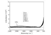
- the rutile-type titanium oxide electrode 107a subjected to the amorphous surface treatment by the sol-gel method is the same as the rutile-type titanium oxide electrode 207a not subjected to the surface treatment (the same as the rutile-type titanium oxide electrode 201a in Experimental Example 1). , See FIG. 17), it can be seen that the transient absorption intensity has decreased as a whole.
- the anatase-type titanium oxide electrode 107b subjected to the amorphous surface treatment by the sol-gel method is the same as the anatase-type titanium oxide electrode 207b that is not subjected to the surface treatment (because it is the same as the anatase-type titanium oxide electrode 201b in Experimental Example 1).
- the transient absorption intensity is generally reduced.
- Rutile titanium oxide electrode 107a As shown in FIG. 24, the wave number 1000 cm -1 or 8000 cm -1 The following wavenumber ranges, having an absorption peak at a wavenumber of 5800cm -1. Further, the wave number 1000 cm -1 or 20000 cm -1 or less wavenumber range, with a maximum of the transient absorption intensity at a wavenumber of 20000 cm -1.
- Table 7 the ratio of the transient absorption intensity at a wavenumber 15000 cm -1 It was shown to.
- the rutile-type titanium oxide electrode 107a has a transient absorption intensity at an absorption peak (wave number 5800 cm ⁇ 1 ) that is about 0.35 times the transient absorption intensity at a wave number 15000 cm ⁇ 1 .
- the rutile-type titanium oxide electrode 107a subjected to the amorphous surface treatment by the sol-gel method has a ratio of the transient absorption intensity at the wave number of 15000 cm ⁇ 1 to the transient absorption intensity at the absorption peak (wave number of 5800 cm ⁇ 1 ) of less than 10 times. Therefore, it can be said that the photocatalytic activity is low.
- rutile titanium oxide electrode 107a is transient absorption intensity at wave number 1000 cm -1 is, it can be seen that the relative transient absorption intensity at a wavenumber 15000 cm -1 is about 0.049 times.
- the anatase-type titanium oxide electrode 107b has a maximum transient absorption intensity at a wave number of 1000 cm ⁇ 1 in a wave number range of a wave number of 20000 cm ⁇ 1 or less.
- anatase titanium oxide electrode 107b is transient absorption intensity at wave number 1000 cm -1 indicating the maximum value of the transient absorption intensity is about 7.3 times the transient absorption intensity at a wavenumber 15000 cm -1 I understand that.
- an amorphous surface treated anatase type titanium oxide electrode 107b by a sol-gel method 10 times the ratio of the transient absorption intensity at a wave number 15000 cm -1 to transient absorption intensity at a wave number 1000 cm -1 indicating the maximum value of the transient absorption intensity Therefore, it can be said that the photocatalytic activity is low.
- an amorphous aluminum oxide (Al 2 O 3 ) layer having a thickness of 1 nm is formed on the surface of the amorphous titanium oxide layer using an atomic layer deposition apparatus under a temperature condition of 100 ° C., and the covering layer and the protective layer A rutile-type titanium oxide electrode 108b provided with
- the rutile-type titanium oxide electrode 108b provided with the coating layer and the protective layer has a larger current density, a slow attenuation, and durability compared to the rutile-type titanium oxide electrode 108a provided with only the coating layer. It was excellent. From this, it is considered that the protective layer of amorphous aluminum oxide has the effect of further improving the catalytic activity by protecting the coating layer of amorphous titanium oxide.
- amorphous aluminum oxide layer (second metal compound layer) having a thickness of 4 nm is formed on the surface of the rutile-type titanium oxide electrode 208 (first metal compound) using an atomic layer deposition apparatus under a temperature condition of 100 ° C., A rutile-type titanium oxide electrode 108c was obtained. Similarly, the rutile-type titanium oxide electrode 108c was irradiated with ultraviolet rays to decompose water, and the current density was measured. The results are shown in FIG.
- the rutile titanium oxide electrode 108c having an amorphous aluminum oxide layer has the same current density as that of the rutile titanium oxide electrode 208, and the activity was maintained.
- the rutile-type titanium oxide electrode 108b having a coating layer and a protective layer exhibits high catalytic activity when irradiated with visible light. Further, since the rutile titanium oxide electrode 108b has a higher current density than the rutile titanium oxide electrode 108a, it can be seen that the catalytic activity is further improved by providing a protective layer on the surface of the coating layer.
- the rutile-type titanium oxide electrode 108b provided with the coating layer and the protective layer has absorption in the visible light region, and it can be seen that the photocatalytic activity is expressed by irradiation with visible light. Further, since the rutile type titanium oxide electrode 108b generally has higher absorption strength than the rutile type titanium oxide electrode 108a, higher catalytic activity can be obtained by having a protective layer of amorphous aluminum oxide. Recognize.
- the rutile titanium oxide electrode 108a having the amorphous titanium oxide coating layer has a catalytic activity as compared with the rutile titanium oxide electrode 108c having the amorphous aluminum oxide coating layer. It is high. From this, it can be seen that, as the coating layer, the activity is easily improved when the valence of the metal cation is equal to or less than the valence of the metal cation of the photocatalyst.
- Example 9 (Formation of protective layer made of amorphous aluminum oxide: anatase-type titanium oxide)
- an amorphous layer having a thickness of 4 nm was formed as a coating layer at a temperature of 100 ° C. using an atomic layer deposition apparatus.
- a titanium oxide layer (second metal compound layer) was formed to obtain an anatase-type titanium oxide electrode 109a according to the present invention.
- an amorphous aluminum oxide (Al 2 O 3 ) layer having a thickness of 1 nm is formed on the surface of the amorphous titanium oxide layer using an atomic layer deposition apparatus at a temperature of 100 ° C.
- An anatase-type titanium oxide electrode 109b having a layer was obtained.
- the anatase-type titanium oxide electrode 209, the anatase-type titanium oxide electrode 109a having a coating layer, and the anatase-type titanium oxide electrode 109b having a coating layer and a protective layer are continuously irradiated with ultraviolet rays having a wavelength of 375 nm in the same manner as in Experimental Example 8. Then, water was decomposed and the current density was measured. The results are shown in FIG.
- the anatase-type titanium oxide electrode 109b having a coating layer and a protective layer has a slow decay of current density and excellent durability compared to the anatase-type titanium oxide electrode 109a having only a coating layer. It was. From this, it is considered that the protective layer of amorphous aluminum oxide has the effect of further improving the catalytic activity by protecting the coating layer of amorphous titanium oxide.
- an amorphous aluminum oxide layer (second metal compound layer) having a thickness of 4 nm is formed on the surface of the anatase-type titanium oxide electrode 209 (first metal compound) by an atomic layer deposition apparatus at a temperature of 100 ° C.
- an anatase-type titanium oxide electrode 109c according to the present invention was obtained.
- the anatase type titanium oxide electrode 109c it carried out similarly to the experiment example 8, and irradiated the ultraviolet-ray, water was decomposed
- anatase-type titanium oxide electrode 109c having an amorphous aluminum oxide layer has a higher current density and improved activity compared to the anatase-type titanium oxide electrode 209.
- the anatase-type titanium oxide electrode 109b provided with the coating layer and the protective layer exhibits high catalytic activity when irradiated with visible light.
- the anatase-type titanium oxide electrode 109b has a higher current density than the anatase-type titanium oxide electrode 109a, and thus it can be seen that the catalytic activity is further improved by providing a protective layer on the surface of the coating layer.
- the anatase-type titanium oxide electrode 109b provided with the coating layer and the protective layer shows absorption in the visible light region and exhibits photocatalytic activity by irradiation with visible light.
- the anatase-type titanium oxide electrode 109b has higher overall absorption strength than the anatase-type titanium oxide electrode 109a, higher catalytic activity can be obtained by having a protective layer of amorphous aluminum oxide. Recognize.
- the anatase-type titanium oxide electrode 109a having the amorphous titanium oxide coating layer has catalytic activity as compared with the anatase-type titanium oxide electrode 109c having the amorphous aluminum oxide coating layer. It is high. From this, it can be seen that, as the coating layer, the activity is easily improved when the valence of the metal cation is equal to or less than the valence of the metal cation of the photocatalyst.
- anatase-type titanium oxide electrodes 110a to 110e according to Experimental Example 10 will be described.
- an amorphous titanium oxide coating layer (second metal compound layer) having a thickness of 4 nm was formed on the surface of anatase-type titanium oxide (first metal compound) using an atomic layer deposition apparatus.
- an anatase-type titanium oxide electrode 110a according to the present invention was obtained.
- annealing was performed in the atmosphere for 1 hour at a temperature of 200 ° C. to obtain an anatase type titanium oxide electrode 110b.
- anatase-type titanium oxide electrodes 110c to 110e were manufactured in the same manner as the anatase-type titanium oxide electrode 110b except that the annealing temperature was changed to 300 ° C., 400 ° C., and 500 ° C.
- a silver / silver chloride electrode is used as a reference electrode
- a 0.1 M Na 2 SO 4 aqueous solution is used as an electrolyte
- an LED lamp manufactured by Thorlabs, M375L3
- Water was decomposed by irradiating ultraviolet rays at 0.1 Hz intermittently (50 mW / cm 2 ), and the current density was measured to evaluate the water decomposition activity.
- the current density was measured using a potentio galvanostat (PS-14, manufactured by Toho Giken Co., Ltd.) while changing the applied potential from ⁇ 0.8 V to 1.0 V at a rate of 10 mV / s with respect to the reference electrode. This was done by measuring the oxidation current due to the oxidation of water. The results are shown in FIG.
- the anatase-type titanium oxide electrodes 110b to 110e that were annealed after the formation of the coating layer had a lower current density than the anatase-type titanium oxide electrodes 110a that were not annealed. From this, it can be seen that the catalytic activity decreases.
- the rutile titanium oxide electrodes 111b to 111e that were annealed after the coating layer was formed had a lower current density than the rutile titanium oxide electrodes 111a that were not annealed. From this, it can be seen that the catalytic activity decreases.
Landscapes
- Chemical & Material Sciences (AREA)
- Engineering & Computer Science (AREA)
- Materials Engineering (AREA)
- Organic Chemistry (AREA)
- Chemical Kinetics & Catalysis (AREA)
- Physics & Mathematics (AREA)
- Health & Medical Sciences (AREA)
- Plasma & Fusion (AREA)
- Toxicology (AREA)
- Catalysts (AREA)
- Inorganic Compounds Of Heavy Metals (AREA)
Abstract
高い光触媒活性を有する構造物及びその製造方法を提供する。一の実施形態に係る構造物は、第1の結晶構造を有する第1の金属化合物と、前記第1の金属化合物の表面に位置し、前記第1の結晶構造と異なる第2の構造を有する第2の金属化合物層と、を備え、表面に前記第2の金属化合物層を有する前記第1の金属化合物は、レーザーパルス照射の5μs後に測定した時間分解分光測定において、1000cm-1以上20000cm-1以下の波数範囲内における過渡吸収強度の最大値が、1000cm-1以上8000cm-1以下の波数範囲に存在し、波数15000cm-1における過渡吸収強度に対する前記最大値の過渡吸収強度の比が10倍以上であることを特徴とする。
Description
本発明は、光触媒活性を有する構造物及びその製造方法に関する。
酸化チタン(TiO2)は、励起光を照射することにより光触媒活性を発現することが知られている。酸化チタンをはじめとする金属酸化物や金属酸窒化物、金属窒化物、金属硫化物などの光触媒活性を有する金属化合物は、様々な分野において用いられている。
このような金属化合物の表面には、酸素欠陥や窒素欠陥、硫黄欠陥、金属欠損、金属挿入欠陥などが存在する。欠陥の周辺にある原子は、励起された電子や正孔などの光励起キャリアーを捕捉し、電子と正孔が有する反応活性を低下させる。また、電子と正孔との再結合速度が速くなることで、光触媒活性が低下するという問題がある。
光触媒活性を向上するために種々の提案がなされており、例えば特許文献1には、水分解用光電極において、n型半導体を含む光触媒層の表面に、p型半導体を含む被覆層を設けた電極とすることで、オンセットポテンシャルを向上させることが記載されている。
特許文献2には、半導体の表面に2種類の異なるナノクラスター(アモルファス状酸化物のナノクラスター(A)及び酸化物ナノクラスター(B))を担持させることにより、顕著な光触媒作用を発現する光触媒材料とすることが記載されている。
非特許文献1には、光触媒の構造上の欠陥によって光励起キャリアーのトラップ準位が深くなり、光触媒活性が小さくなること、光励起キャリアーのトラップ準位は過渡吸収スペクトルによって評価できることが記載されている。また、チタン酸ストロンチウム(SrTiO3)粒子を溶融塩(塩化ストロンチウム(SrCl2))の中で加熱(フラックス処理)し、再結晶化させ、チタン酸ストロンチウム粒子の結晶欠陥を低減することで、キャリアーのトラップ準位が浅くなり、光触媒活性を向上できたことが記載されている。
Akira Yamakata, Ham Yeilin, Masayuki Kawaguchi, Takashi Hisatomi, Jun Kubota, Yoshihisa Sakata, and Kazunari Domen. Morphology-sensitive Trapping States of Photogenerated Charge Carriers on SrTiO3 Particles Studied by Time-resolved Visible to Mid-IR Absorption Spectroscopy: the Effects of Molten Salt Flux Treatments. J. PhotoChem. Photobiol. A - chem. 313, 168-175 (2015).
しかし、特許文献1に記載の光電極は、表1に示されるように、基準電圧1.2Vにおける光電流密度が最大でも4mA/cm2(実施例2の窒化タンタル電極)であり、被覆層を有しない光電極(比較例1の窒化タンタル電極等)と比較して、触媒活性が有意に向上したとはいえない。また、特許文献1においては、光電極の活性が向上するメカニズムについての検討が全くなされていない。特許文献2に記載の光触媒材料は、可視光の照射による光触媒活性を向上させているが、さらなる改善の余地がある。
非特許文献1に記載のフラックス処理は、光触媒の構造上の欠陥をナノオーダーで被覆することが難しく、キャリアーのトラップ準位を浅くすることによる光触媒活性の向上には限界がある。さらに、溶融塩の陽イオンが光触媒の金属化合物と結合して組成や構造が変化してしまい、光触媒活性が低下する場合がある。
そこで、本発明は、光励起キャリアーのトラップ準位が浅く、高い光触媒活性を有する構造物及びその製造方法を提供することを目的とする。
本発明者らは、光触媒の結晶構造と異なる構造を有する金属化合物のナノ皮膜によって、光触媒の表面に存在する構造上の欠陥を被覆することで、トラップ準位を浅くすることができ、自由電子が増加することにより光触媒活性が改善されることを見出し、本発明を完成させた。
すなわち、本発明の構造物は、第1の結晶構造を有する第1の金属化合物と、前記第1の金属化合物の表面に位置し、前記第1の結晶構造と異なる第2の構造を有する第2の金属化合物層と、を備え、表面に前記第2の金属化合物層を有する前記第1の金属化合物は、レーザーパルス照射の5μs後に測定した時間分解分光測定において、1000cm-1以上20000cm-1以下の波数範囲内における過渡吸収強度の最大値が、1000cm-1以上8000cm-1以下の波数範囲に存在し、波数15000cm-1における過渡吸収強度に対する前記最大値の過渡吸収強度の比が10倍以上であることを特徴とする。
あるいは、本発明の構造物は、第1の結晶構造を有する第1の金属化合物と、前記第1の金属化合物の表面に位置し、前記第1の結晶構造と異なる第2の構造を有する第2の金属化合物層と、を備え、前記第2の金属化合物層は、厚さが10nm以下であり、表面に前記第2の金属化合物層を有する前記第1の金属化合物は、時間分解分光測定において第1の波数未満の波数範囲に吸収ピークを有することを特徴とする。
上記いずれかの場合において、前記第2の金属化合物層は、厚さが10nm以下であることが好ましい。
上記いずれかの場合において、前記第2の金属化合物層の表面に、前記第1の結晶構造と異なる第3の構造を有する保護層をさらに備えることが好ましい。
上記の場合において、前記第2の構造がアモルファス構造であることが好適である。
上記の場合において、前記第3の構造がアモルファス構造であることが好適である。
上記の場合において、前記過渡吸収強度の比が100倍以上であることが好ましい。
上記の場合において、前記第1の金属化合物が光触媒であることが好ましい。
上記の場合において、前記第1の金属化合物及び前記第2の金属化合物が金属酸化物、金属窒化物、金属酸窒化物、金属硫化物及び金属酸硫化物のいずれかであることが好ましい。
さらに、前記第1の金属化合物は、励起光により励起したときの発光スペクトルの発光ピークを第1の波長域に有し、表面に前記第2の金属化合物層を有する前記第1の金属化合物は、前記発光スペクトルの発光ピークを前記第1の波長域よりも小さい第2の波長域に有し、且つ前記第2の波長域における前記第2の金属化合物層の発光強度が、前記第2の波長域における前記第1の金属化合物の発光強度よりも大きいことが好ましい。
また、本発明の構造物の製造方法は、第1の結晶構造を有する第1の金属化合物の表面に、前記第1の結晶構造と異なる第2の構造を有する第2の金属化合物層を形成する工程を備え、前記第2の金属化合物層は、原子層堆積装置により形成され、表面に前記第2の金属化合物層を有する前記第1の金属化合物は、レーザーパルス照射の5μs後に測定した時間分解分光測定において、1000cm-1以上20000cm-1以下の波数範囲内における過渡吸収強度の最大値が、1000cm-1以上8000cm-1以下の波数範囲に存在し、波数15000cm-1における過渡吸収強度に対する前記最大値の過渡吸収強度の比が10倍以上であることを特徴とする。
あるいは、本発明の構造物の製造方法は、第1の結晶構造を有する第1の金属化合物の表面に、前記第1の結晶構造と異なる第2の構造を有する第2の金属化合物層を形成する工程を備え、表面に前記第2の金属化合物層を有する前記第1の金属化合物は、時間分解分光測定において第1の波数未満の波数範囲に吸収ピークを有し、前記第2の金属化合物層は、原子層堆積装置により厚さが10nm以下となるように形成されることを特徴とする。
上記いずれかの場合において、前記第2の金属化合物層は、厚さが10nm以下となるように形成されることが好ましい。
上記いずれかの場合において、前記第2の金属化合物層の表面に、前記第1の結晶構造と異なる第3の構造を有する保護層を形成する工程をさらに備えることが好ましい。
上記の場合において、前記第2の構造がアモルファス構造であることが好適である。
上記の場合において、前記第3の構造がアモルファス構造であることが好適である。
上記の場合において、前記第1の金属化合物が光触媒であることが好ましい。
上記の場合において、前記第1の金属化合物及び前記第2の金属化合物が金属酸化物、金属窒化物、金属酸窒化物、金属硫化物及び金属酸硫化物のいずれかであることが好ましい。
以上のように、本発明に係る構造物及びその製造方法によれば、光触媒の結晶構造と異なる構造を有する金属化合物のナノ皮膜を有することで、光励起キャリアーのトラップ準位を浅くすることができ、光触媒活性を向上することができる。
以下、図面を参照して本発明の実施形態について詳細に説明する。
[第1の実施形態]
図1~4を参照して、第1の実施形態に係る構造物100について説明する。図1は、第1の実施形態に係る構造物100の概略構成を示す断面図である。図2は、本実施形態に係る金属化合物1のエネルギーバンドを示す模式図である。図3及び図4は、本実施形態に係る構造物100の一例を示す模式図である。
図1~4を参照して、第1の実施形態に係る構造物100について説明する。図1は、第1の実施形態に係る構造物100の概略構成を示す断面図である。図2は、本実施形態に係る金属化合物1のエネルギーバンドを示す模式図である。図3及び図4は、本実施形態に係る構造物100の一例を示す模式図である。
図1の右側に示すように、本実施形態に係る構造物100は、金属化合物1(第1の金属化合物)及び金属化合物1の表面に配置された被覆層2(第2の金属化合物層)を備える。
金属化合物1としては、励起光(紫外線、可視光、又は近赤外線)の照射により光触媒活性を発現するものを使用することができ、例えば酸化チタン(TiO2)や酸化タングステン(WO3)、酸化タンタル(Ta2O5)、酸化ガリウム(Ga2O3)などの金属酸化物、窒化タンタル(TaN)や窒化ガリウム(GaN)などの金属窒化物、酸窒化タンタル(TaON)やランタンチタン酸窒化物(LaTiO2N)などの金属酸窒化物、硫化亜鉛(ZnS)や硫化カドミウム(CdS)、硫化水銀(HgS)、硫化モリブデン(MoS2)などの金属硫化物、Sm2Ti2S2O5などの金属酸硫化物等の金属化合物が挙げられる。これらの金属化合物のうち、1種を単独で用いることも、2種以上を併用して2種以上の金属元素を有する複合金属化合物とすることもできる。これらのうち、光触媒として広く用いられていることなどから、酸化チタン、酸化タングステンが特に好ましい。なお、金属化合物1の結晶構造(本発明における第1の結晶構造)は、非晶質(アモルファス)構造以外の構造である。
図1の左側や図3に示すように、金属化合物1の表面構造は均一ではなく、酸素欠陥や窒素欠陥、硫黄欠陥、金属欠損、金属挿入欠陥等の表面欠陥が存在する。図2に示すように、金属化合物1にバンドギャップ以上の光エネルギー(hν)を照射すると、励起された電子e-は価電子帯VBから伝導帯CBに移動するが、その後数ピコ秒のうちに、表面欠陥によるトラップ準位TBにトラップされる。この表面欠陥によるトラップ準位TBが深いことにより、金属化合物1の光触媒活性が落ちてしまう。以下、トラップ準位TBにトラップされた電子を「トラップ電子」ということがある。
金属触媒である金属化合物1の形状や大きさとして特に限定はなく、層状、粒子状、柱状など、任意の形状とすることができる。なお、図示は省略しているが、金属化合物1は、石英ガラス基板、FTOガラス基板、CaF2基板等の各種基板や、その他の支持体上に設けられていてもよい。
被覆層2は、金属化合物1の表面欠陥を埋めるように堆積された層である。構造物100の最外部に位置してもよく、さらにその表面の保護層を備えていてもよい。被覆層2の堆積方法として、種々の公知の方法を採用することができ、特に、後述する原子層堆積装置(Atomic Layer Deposition(ALD)装置)を用いて堆積することが好ましい。被覆層2は、金属化合物1の表面全体に堆積されていてもよいし、金属化合物1の表面の一部のみに堆積されていてもよい。また、被覆層2は、金属化合物1の欠陥上にのみ堆積されていてもよい。
被覆層2は、金属化合物1の結晶構造と異なる構造(本発明の第2の構造)の金属化合物から構成される。ここで、異なる構造とは、金属化合物1とは異なる結晶構造、非晶質構造、結晶・非晶質の混合構造を意味する。被覆層2の構造としては、例えば結晶構造であればアナターゼ型、ルチル型などを挙げることができる。被覆層2の構造としては、金属化合物1の表面欠陥に起因する構造的ひずみを抑制でき、自身に欠陥が少ないものが好ましい。この観点から、被覆層2としては、特に非晶質(アモルファス)構造が最も好ましい。この場合において、アモルファス構造には、ルチル型及び/又はアナターゼ型の結晶構造が一部に含まれていてもよい。また、被覆層2が結晶構造の場合、ルチル型よりもアナターゼ型が好ましい。
被覆層2を構成する金属化合物として、金属化合物1と同様のものを使用することができ、例えば酸化チタン(TiO2)や酸化タングステン(WO3)、酸化タンタル(Ta2O5)、酸化ガリウム(Ga2O3)、酸化アルミニウム(Al2O3)、酸化ジルコニウム(ZrO2)などの金属酸化物、窒化タンタル(TaN)や窒化ガリウム(GaN)などの金属窒化物、酸窒化タンタル(TaON)やランタンチタン酸窒化物(LaTiO2N)などの金属酸窒化物、硫化亜鉛(ZnS)や硫化カドミウム(CdS)、硫化水銀(HgS)、硫化モリブデン(MoS2)などの金属硫化物、Sm2Ti2S2O5などの金属酸硫化物等の金属化合物が挙げられる。これらの金属化合物のうち、1種を単独で用いることも、2種以上を併用して2種以上の金属元素を有する複合金属化合物とすることもできる。これらのうち、酸化チタン、酸化タングステン、酸化タンタルが特に好ましい。金属化合物1と被覆層2との組み合わせとして、被覆層2の金属カチオンの価数が、金属化合物1の金属カチオンの価数と同じか、それよりも小さな価数であることが好ましい。例えば、金属化合物1が酸化チタンである場合、Tiの価数は4+であるため、被覆層2の金属カチオンはTi4+、Si4+、Zr4+、Ga3+、Al3+、Zn2+などであることが好ましく、Cr6+やW6+などは好ましくない。これは、原子価が大きくなると被覆層2自体が電子を引きつけて捕捉する傾向にあるためである。
被覆層2の厚さは特に制限はないが、通常は20nm以下であり、0.1nm~10nmであることが好ましく、0.2nm~7nmであることがより好ましい。被覆層2の厚さが20nm以下であれば、被覆層2によって吸収される光が少なく、また、金属化合物1の励起された電子の移動が阻害されにくいため、金属化合物1による光触媒活性を高くすることができる。なお、0.1nmより小さい、あるいは10nmより大きいと、光触媒活性を向上させることが困難になりやすい。なお、本実施形態において、被覆層2は金属化合物1と同様の金属化合物から構成されるが、その厚さが0.1nm~10nmであることにより、光触媒活性を有しないか、低くなる。
図3において、金属化合物1がルチル型又はアナターゼ型酸化チタンであり、被覆層2がアモルファス酸化チタンである例を示している。また、図4において、金属化合物1がルチル型又はアナターゼ型酸化チタンであり、被覆層2がアモルファス酸化ガリウム及びアモルファス酸化タンタルである例を示している。このように、金属化合物1の表面に配置される被覆層2は、当該金属化合物1と異なる結晶構造を有し、且つ当該金属化合物1と同一又は異なる組成の金属化合物とすることができる。また、図4に示す例のように、異なる組成の複数の金属化合物を用いて、被覆層2として、2種以上の金属元素を有する複合金属化合物とすることができる。なお、図3及び図4において、金属化合物1及び被覆層2の結晶構造(原子配置)は模式的に示したものであり、実際のものとは異なっている場合がある。
被覆層2の表面には、保護層(不図示)を設けてもよい。保護層は、被覆層2の表面を保護する目的の層であり、光触媒活性の向上と耐久性の増加に寄与する。保護層を構成する化合物としては、酸化アルミニウム、酸化ジルコニウム(ZrO2)、二酸化ケイ素(シリカ)などを挙げることができる。保護層は、金属化合物1の結晶構造と異なる構造(第3の構造)を有する化合物から構成される。保護層の構造と被覆層2の構造は、互いに同一であってもよいし、異なっていてもよい。保護層の構造としては、非晶質(アモルファス)構造が最も好ましい。保護層の厚さは、通常は5nm以下であり、0.1~3nmの範囲が好ましい。保護層の厚さが厚すぎると、保護層による光の吸収や、金属化合物1の励起された電子の移動が阻害されることによって構造物の光触媒活性が低くなりやすい。保護層は、被覆層2の表面の全体に設けられていてもよいし、表面の一部に設けられていてもよい。また、被覆層2が金属化合物1の表面の一部に設けられている場合、金属化合物1の表面にも保護層が配置されていてもよい。
本発明の構造物100(表面に第2の金属化合物層を有する第1の金属化合物)は、レーザーパルス照射の5μs後に測定した時間分解分光測定において、1000cm-1以上20000cm-1以下の波数範囲内における過渡吸収強度の最大値が、1000cm-1以上8000cm-1以下の波数範囲に存在し、波数15000cm-1における過渡吸収強度に対するこの最大値の過渡吸収強度の比が10倍以上である。ここで、過渡吸収強度の最大値は、後述する図18のように過渡吸収強度の吸収ピークを示す位置における過渡吸収強度の値である場合と、後述する図21のように吸収ピークを示さないが吸収を示す位置における過渡吸収強度の値である場合とを含む。
ここで、本発明の構造物100が高い光触媒活性を有する点について説明する。金属化合物1の自由電子(Free e-)は光触媒活性に寄与しており、その数が多いほど光触媒活性が高くなる。表面に被覆層2を備えていない金属化合物1は、表面欠陥を有しており、この表面欠陥は金属化合物1の電荷のバランスなどにひずみを引き起こす。これにより、金属化合物1には、深い欠陥準位に捕捉された電子(trapped e-)や正孔(trapped h+)が多く含まれる。光の照射によって励起された電子は、この捕捉された電子や正孔にトラップされ、その結果、光触媒活性が低下する。
これに対して、金属化合物1の表面に被覆層2を形成すると、金属化合物1の表面欠陥が埋まり、欠陥構造が変化し、電荷のバランスなどのひずみが低減され、欠陥準位の深さが浅くなる。これにより、電子と正孔の反応性が上がり、光触媒活性が向上する。被覆層2は、金属化合物1のひずみを低減する構造のものであればどのような構造でもよいが、金属化合物1と同じ結晶構造の場合はひずみを低減できないため、金属化合物1とは異なる構造である必要がある。
一般に、自由電子(Free e-)は、中赤外からマイクロ波領域に強い吸収を与えるため、時間分解分光測定による過渡吸収スペクトルにおいて波数が0cm-1に向かうにつれて吸収強度が高くなり、0cm-1近傍に吸収ピークを有する(後述する図15参照)。一方、深い欠陥準位に捕捉された電子(trapped e-)や正孔(trapped h+)は、可視光~近赤外領域に吸収を与える。したがって、電子を捕捉するトラップ準位TBが浅くなれば、トラップ電子が与える吸収波長は長波長側にシフトするため、時間分解分光測定による過渡吸収スペクトルにおいて波数10000cm-1~15000cm-1の吸収強度が高くなる。したがって、時間分解分光測定による過渡吸収スペクトルを測定すれば、自由電子、捕捉された電子、正孔の挙動を独立に評価することができる。
本発明の構造物100は、例えば図18に示すように、1000cm-1以上8000cm-1以下の波数範囲に吸収ピークを有し、吸収ピークにおける過渡吸収強度は、波数が1000cm-1以上20000cm-1以下の範囲内における過渡吸収強度の最大値を示す。これは、捕捉された電子や正孔に起因する吸収が小さく、光によって励起された自由電子に起因する吸収が大きいことを意味する。すなわち、被覆層2を備えることで、金属化合物1の表面欠陥が埋まり、捕捉された電子や正孔の欠陥準位が浅くなっていることを意味する。この結果、表面欠陥によってトラップされる励起電子が少なくなり、光触媒活性が向上する。仮に捕捉された電子や正孔が全くなくなった場合、励起された自由電子のみとなるため、過渡吸収強度の最大値を示す波数は0cm-1近傍となる。上記のメカニズムは、酸化チタンや酸化タングステンといった特定の光触媒化合物に限定されるものではなく、他の様々な光触媒化合物にも当てはまる。
本発明の構造物100は、波数15000cm-1における過渡吸収強度に対する上記の最大値の比(過渡吸収強度比)が10倍以上であり、15倍以上であることが好ましく、30倍以上であることがより好ましく、100倍以上であることが特に好ましい。波数15000cm-1における過渡吸収強度に対して上記の最大値が10倍以上であることで、自由電子の数や浅い欠陥準位に捕捉された電子の数が十分多く、光触媒活性が高くなっているといえる。
本実施形態に係る金属化合物1は、時間分解分光測定による過渡吸収スペクトルにおいて、第1の波数(例えば、7000cm-1)以上の波数範囲に吸収ピークを有する。また、金属化合物1の表面に被覆層2を有する構造物100は、時間分解分光測定による過渡吸収スペクトルにおいて、第1の波数(例えば7000cm-1)未満の波数範囲に吸収ピークを有する。このように、構造物100の過渡吸収スペクトルは、金属化合物1のみの過渡吸収スペクトルと比較して、より低波数側に吸収ピークを有する。また、構造物100の過渡吸収スペクトルは、金属化合物1の過渡吸収スペクトルと比較して、低波数側において吸収強度が大きくなる。
一般に、光触媒として用いられる金属化合物のトラップ準位は、発光スペクトル測定を行い、トラップに捕捉されたキャリアーの再結合による発光ピークの位置により見積もることができる。金属化合物1の発光スペクトルにおいて、700nm以上の長波長側に現れる発光ピークは、深いトラップ準位に落ち込んだトラップ電子に由来する。また、700nm未満の短波長側に現れる発光ピークは、浅いトラップ準位に落ち込んだトラップ電子又は自由電子に由来する。このことは、非特許文献(Xiuli Wang, Zhaochi Feng, Jianying Shi, Guoqing Jia, Shuai Shen, Jun Zhou and Can Li. Trap states and carrier dynamics of TiO2 studied by photoluminescence spectroscopy under weak excitation condition. Phys. 2010, 12, 7083?7090.)に記載されている。従って、発光スペクトル測定における発光ピークが700nm未満の波長領域にある場合、光触媒活性が高いといえる。
金属化合物1は、励起光により励起したときの発光スペクトルにおいて、第1の波長(例えば、700nm)より長波長側の第1の波長域(例えば、700nm以上の波長域)に発光ピークを有する。一方、本発明の構造物100は、励起光により励起したときの発光スペクトルにおいて、第1の波長(例えば、700nm)より短波長側の第2の波長域(例えば、700nm未満の波長域)に発光ピークを有する。例えば、後述する図13に示すように、金属化合物1がルチル型酸化チタン204である場合、該ルチル型酸化チタン204は、励起光により励起したときの発光スペクトルにおいて、発光ピークを840nmに有する。一方、ルチル型酸化チタンの表面にアモルファス酸化チタン層を有する構造物104は、発光ピークを500nmに有する。
また、金属化合物1の表面に被覆層2を有する構造物100は、第2の波長域における発光強度が、金属化合物1の発光強度よりも大きい。このように、構造物100の発光スペクトルは、金属化合物1のみの発光スペクトルと比較して、第1の波長より短波長側の波長域(第2の波長域)に発光ピークを有する。また、構造物100の発光強度は、金属化合物1の発光強度と比較して、第1の波長より短波長側の波長域(第2の波長域)において大きくなる。例えば図13に示すように、表面にアモルファス酸化チタン層を有する構造物104は、700nm未満の波長域において、ルチル型酸化チタン204よりも発光強度が大きくなっている。
また、金属化合物1の表面に被覆層2を有する構造物100は、第2の波長域における発光強度が、金属化合物1の発光強度よりも大きい。このように、構造物100の発光スペクトルは、金属化合物1のみの発光スペクトルと比較して、第1の波長より短波長側の波長域(第2の波長域)に発光ピークを有する。また、構造物100の発光強度は、金属化合物1の発光強度と比較して、第1の波長より短波長側の波長域(第2の波長域)において大きくなる。例えば図13に示すように、表面にアモルファス酸化チタン層を有する構造物104は、700nm未満の波長域において、ルチル型酸化チタン204よりも発光強度が大きくなっている。
本実施形態に係る構造物100は、光触媒材料としてあらゆる分野における各種用途に用いることができ、例えば、光触媒電極、金属酸化物薄膜透明電極、色素増感太陽電池、ペロブスカイト太陽電池、防曇・防汚材料、抗菌材料等に応用することができる。
[製造方法]
次に、第1の実施形態に係る構造物100の製造方法について説明する。本実施形態に係る構造物100の製造方法は、図1に示すように、表面欠陥を有する金属化合物1の表面に、原子層堆積装置(ALD装置)を用いて、厚さが0.1nm~10nmとなるように被覆層2を形成する工程を有する。
次に、第1の実施形態に係る構造物100の製造方法について説明する。本実施形態に係る構造物100の製造方法は、図1に示すように、表面欠陥を有する金属化合物1の表面に、原子層堆積装置(ALD装置)を用いて、厚さが0.1nm~10nmとなるように被覆層2を形成する工程を有する。
原子層堆積装置は、原子層毎の成膜を可能とするため、非常に薄い膜を形成する場合に適している。原子層堆積法(ALD法)は一般に、2種類以上のガス状の原料を反応室に交互に供給し、膜形成面で化学反応を起こして成膜する方法であり、1サイクルで原子層相当レベルの厚みを高精度に形成することができる。原子層堆積装置として、公知の装置を用いることができる。なお、被覆層2の形成方法として、ゾルゲル法やCVD(Chemical Vapor Deposition)法は、被覆層2の厚さを制御することが困難となり、光触媒活性が低下する場合がある。
原子層堆積装置による被覆層2の形成は、80℃~400℃の条件下で行われることが好ましく、80℃~300℃がより好ましい。被覆層2を形成する温度によって、被覆層2の構造を変えることが可能である。例えば、被覆層2が酸化チタンの場合、被覆層2の形成温度が300℃以下であればアモルファス構造となり、これを超えると一部にアナターゼ型の結晶構造が混じり、500℃以上ではほぼアナターゼ型の結晶構造となる。
なお、金属化合物1の表面に被覆層2を形成する工程の前に、金属化合物1を、FTOガラス基板やCaF2基板等の各種支持体上に固定する工程を有していてもよい。支持体上に金属化合物1を固定する方法として特に限定はなく、金属化合物1の粉末を塗布して焼結する方法など、任意の方法を採用することができる。
また、金属化合物1の表面に被覆層2を形成する工程の前に、前処理として金属化合物1の表面をUV(紫外線)オゾン処理する工程を有していてもよい。UVオゾン処理の条件は特に制限されないが、供給される酸素の流量は1~10ml/minが好ましい。また、処理時間は、3~20分間が好ましい。また、照射されるUVの波長領域は、185nm~254nmが好ましく、出力は20~45Wが好ましく、照射強度は2000~3500μW/cm2が好ましい。
また、被覆層2を形成した後、必要に応じて、アニール処理工程を実施してもよい。アニール処理の条件は特に制限されないが、加熱温度は100℃~800℃が好ましく、100℃~500℃がより好ましい。また、加熱時間は0.25時間~1.5時間が好ましく、0.5時間~1時間がより好ましい。なお、アニール処理の方法は特に制限されず、公知のオーブンなどを使用できる。ただし、アニール処理を行わなかった場合と比較して、アニール処理を行うことにより、光触媒活性が低下する場合がある。これは、アニール処理を行うことによって被覆層2の構造が変化し、金属化合物1の結晶構造と同様の構造となる場合があるためであると考えられる。例えば、被覆層2の構造がアモルファス構造である場合、アニール処理により結晶化が促進され、金属化合物1と同じ結晶構造に変化する場合がある。
[実施例]
以下、図5A~図35を参照して、実験例1~11に基づき、従来例及び本発明に係る構造物について具体的に説明するが、本発明はこれにより限定されるものではない。
以下、図5A~図35を参照して、実験例1~11に基づき、従来例及び本発明に係る構造物について具体的に説明するが、本発明はこれにより限定されるものではない。
<実験例1>
(酸化チタン電極における水の分解活性)
図5A~図7Bを参照して、実験例1に係る酸化チタン電極の水の分解活性について説明する。
(酸化チタン電極における水の分解活性)
図5A~図7Bを参照して、実験例1に係る酸化チタン電極の水の分解活性について説明する。
図5Aは、従来例に係る酸化チタン電極201を示す模式図である。図5Bは、表面に被覆層21を有する酸化チタン電極101を示す模式図である。図5Aに示すように、従来例に係る酸化チタン電極201は、FTOガラス基板31上に酸化チタン層11を有する電極であるが、被覆層21を有しない。ここで、酸化チタン層11がルチル型酸化チタン層であるものをルチル型酸化チタン電極201a、酸化チタン層がアナターゼ型酸化チタン層であるものをアナターゼ型酸化チタン電極201bとする。
図5Bに示すように、本発明に係る酸化チタン電極101は、図5Aに示した酸化チタン電極201の酸化チタン層11(第1の金属化合物)の表面に被覆層としてのアモルファス酸化チタン層21(第2の金属化合物層)を形成して得られる電極である。第2の金属化合物層であるアモルファス酸化チタン層21を、電子層堆積装置(Cambridge Nanotech社製、Savannah G2 S100)を用いて100℃の温度条件下において酸化チタン層11上に形成し、被覆層21を有する酸化チタン電極101を得た。ここで、ルチル型酸化チタン電極201aの表面に、厚さ1nm、2nm、3nm、4nm、5nm、6nm、7nm、10nm又は20nmのアモルファス酸化チタン層21をそれぞれ形成し、ルチル型酸化チタン電極101a~101iとした。また、アナターゼ型酸化チタン電極201bの表面に、厚さ1nm、2nm、3nm、4nm、5nm、6nm、7nm、10nm又は20nmのアモルファス酸化チタン層21をそれぞれ形成し、アナターゼ型酸化チタン電極101j~101rとした。
酸化チタン電極101a~101r、201a及び201bのそれぞれについて、基準電極として銀/塩化銀電極、電解液として0.1MのNa2SO4水溶液を用い、LEDランプ(Thorlabs社製、M375L3)を用いて375nmの紫外線を0.1Hzで断続的に照射して(200mW/cm2)水の分解を行い、電流密度を測定して水の分解活性について評価を行った。電流密度の測定は、ポテンショ・ガルバノスタット(東方技研社製、PS-14)を用いて、印加電位を基準電極に対して-0.5Vから1.0Vまで10mV/sの速度で変化させながら、水の酸化による酸化電流を測定することにより行った。
図6Aは、酸化チタン層11がルチル型である酸化チタン電極101a~101i及び201aの水の分解活性を示すグラフである。図6Bは、基準電圧1.0Vにおけるルチル型酸化チタン電極101a~101i及び201aの電流密度を示すグラフである。図7Aは、酸化チタン層11がアナターゼ型である酸化チタン電極101j~101r及び201bの水の分解活性を示すグラフである。図7Bは、基準電圧1.0Vにおけるアナターゼ型酸化チタン電極101j~101r及び201bの電流密度を示すグラフである。なお、図6A及び7Aにおいて、水の分解活性の差異を明瞭にするため、ベースラインをずらして図示している。また、基準電圧1.0Vにおけるルチル型酸化チタン電極101a~101i及び201aの電流密度を表1に示し、基準電圧1.0Vにおけるアナターゼ型酸化チタン電極101j~101r及び201bの電流密度を表2に示した。
図6A及び表1に示すように、被覆層21を有しないルチル型酸化チタン電極201aによる水の分解で生じた電流密度は、基準電圧1.0V、紫外線照射時において0.2mA/cm2である。また、被覆層21を有するルチル型酸化チタン電極101a~101hによる水の分解で生じた電流密度は、基準電圧1.0Vにおいてそれぞれ0.4mA/cm2~13mA/cm2である。被覆層21の厚さが20nmであるルチル型酸化チタン電極101iによる水の分解で生じた電流密度は、基準電圧1.0Vにおいて0.02mA/cm2である。図6A及び表1に示すように、ルチル型酸化チタン電極の水の分解活性は、アモルファス酸化チタン層21の厚さが1nm~5nmと増加するにつれて増加し、5nmである場合(ルチル型酸化チタン電極101e)において最大となることがわかる。

また、図7A及び表2に示すように、被覆層21を有しないアナターゼ型酸化チタン電極201bによる水の分解で生じた電流密度は、基準電圧1.0Vにおいて0.2mA/cm2である。また、被覆層21を有するアナターゼ型酸化チタン電極101j~101qによる水の分解で生じた電流密度は、基準電圧1.0Vにおいてそれぞれ0.5mA/cm2~6.5mA/cm2である。被覆層21の厚さが20nmであるアナターゼ型酸化チタン電極101rによる水の分解で生じた電流密度は、基準電圧1.0Vにおいて0.3mA/cm2である。図7B及び表2に示すように、アナターゼ型酸化チタン電極の水の分解活性は、アモルファス酸化チタン層21の厚さが1nm~5nmと増加するにつれて増加し、5nmである場合(アナターゼ型酸化チタン電極101n)において最大となり、その後厚さが増加するにつれて減少することがわかる。

このように、厚さ1nm~10nmの被覆層21を有するルチル型酸化チタン電極101a~101h及びアナターゼ型酸化チタン電極101j~101qは、酸化チタン電極201a及び201b、厚さ20nmの被覆層21を有する酸化チタン電極101i及び101rと比較して、水の分解によって生じる電流密度が大きくなることがわかる。
<実験例2>
(酸化タングステン電極における水の分解活性)
図8A~図10Bを参照して、実験例2に係る酸化タングステン電極の水の分解活性について説明する。
(酸化タングステン電極における水の分解活性)
図8A~図10Bを参照して、実験例2に係る酸化タングステン電極の水の分解活性について説明する。
図8Aは、従来例に係る酸化タングステン電極202を示す模式図である。図8Bは、表面に被覆層22を有する酸化タングステン電極102を示す模式図である。従来例に係る酸化タングステン電極202は、FTOガラス基板32上に酸化タングステン層12を有するが、被覆層22を有しない。
図8Bに示す酸化タングステン電極102は、図8Aに示した従来の酸化タングステン電極202の酸化タングステン層12(第1の金属化合物)の表面に被覆層22(第2の金属化合物層)を形成した電極である。被覆層22は、電子層堆積装置(ALD)(Cambridge Nanotech社製、Savannah G2 S100)を用いて100℃の温度条件下において酸化タングステン層12上に形成し、被覆層を有するタングステン電極102を得た。ここで、従来の酸化タングステン電極202の表面に、厚さ0.2nm、0.4nm、0.6nm、0.8nm、1nm又は2nmのアモルファス酸化チタンを被覆層22としてそれぞれ形成し、酸化タングステン電極102a~102fとした。また、酸化タングステン電極202の表面に、厚さ0.2nm、0.4nm、0.6nm、0.8nm、1nm又は2nmのアモルファス酸化タンタルを被覆層22としてそれぞれ形成し、酸化タングステン電極102g~102lとした。
酸化タングステン電極102a~102l及び202のそれぞれについて、基準電極として銀/塩化銀電極、電解液として0.1MのNa2SO4水溶液を用い、LEDランプ(Thorlabs社製、M455L3)を用いて455nmの可視光を0.2Hzで断続的に照射して(200mW/cm2)水の分解を行い、電流密度を測定して水の分解活性について評価を行った。電流密度の測定は、ポテンショ・ガルバノスタット(東方技研社製、PS-14)を用いて、印加電位を基準電極に対して0.5Vから1.0Vまで10mV/sの速度で変化させながら水の酸化による酸化電流を測定することにより行った。
図9Aは、被覆層22がアモルファス酸化チタンである場合の水の分解活性を示すグラフである。図9Bは、基準電圧1.0Vにおける酸化タングステン電極102a~102f及び202の電流密度を示すグラフである。図10Aは、被覆層22がアモルファス酸化タンタルである場合の水の分解活性を示すグラフである。図10Bは、基準電圧1.0Vにおける酸化タングステン電極102g~102l及び202の電流密度を示すグラフである。なお、図9A及び10Aにおいて、水の分解活性の差異を明瞭にするため、ベースラインをずらして図示している。
図9A及び9B、図10A及び10Bに示すように、被覆層22を有しない酸化タングステン電極202による水の分解で生じた電流密度は、基準電圧1.0Vにおいて0.85mA/cm2である。また、図9Aに示すように、酸化タングステン電極102b~102eによる水の分解で生じた電流密度は、基準電圧1.0Vにおいて1.5mA/cm2~3.8mA/cm2である。また、酸化タングステン電極102a及び102fによる水の分解で生じた電流密度は、基準電圧1.0Vにおいてそれぞれ0.6mA/cm2、0.2mA/cm2である。
図9Aに示すように、被覆層22として厚さ0.4nm~1nmのアモルファス酸化チタン層を有する酸化タングステン電極102b~102eは、酸化タングステン電極202、厚さ0.2nm、2nmのアモルファス酸化チタン層を有する酸化タングステン電極102a及び102fと比較して、水の分解によって生じる電流密度が大きくなることがわかる。
図9Bに示すように、酸化タングステン電極の水の分解活性は、被覆層22としてのアモルファス酸化チタン層の厚さが0.2nm~1nmと増加するにつれて増加し、1nm(酸化タングステン電極102e)の場合に最大となることがわかる。
また、図10Aに示すように、厚さ0.4nm~2nmのアモルファス酸化タンタル層を有する酸化タングステン電極102h~102lは、酸化タングステン電極202、及び厚さ0.2nmのアモルファス酸化タンタル層を有する酸化タングステン電極102gと比較して、水の分解によって生じる電流密度が大きくなることがわかる。
図10Bに示すように、酸化タングステン電極の水の分解活性は、被覆層22としてのアモルファス酸化タンタル層の厚さが0.2nm~1nmと増加するにつれて増加し、1nm(酸化タングステン電極102k)の場合に最大となることがわかる。
<実験例3>
(アナターゼ型酸化チタン構造物における有機物分解活性)
図11A~図12を参照して、実験例3に係るアナターゼ型酸化チタン構造物の有機物分解性について説明する。
(アナターゼ型酸化チタン構造物における有機物分解活性)
図11A~図12を参照して、実験例3に係るアナターゼ型酸化チタン構造物の有機物分解性について説明する。
図11Aは、従来例に係るアナターゼ型酸化チタン構造物203を示す模式図である。図11Bは、表面にアモルファス酸化チタン層23を有するアナターゼ型酸化チタン構造物103を示す模式図である。図12は、アナターゼ型酸化チタン構造物103及び203における酢酸分解時間と二酸化炭素生成量との関係を示すグラフである。
図11Aに示すアナターゼ型酸化チタン構造物203は、5cm2のFTOガラス基板33上にアナターゼ型酸化チタンの粒子20mgを塗布して固定、焼結させることによりアナターゼ型酸化チタン薄膜23を形成して得られる。図11Bに示すアナターゼ型酸化チタン構造物103は、図11Aに示したアナターゼ型酸化チタン薄膜13(第1の金属化合物)上に、電子層堆積装置(ALD)(Cambridge Nanotech社製、Savannah G2 S100)を用いて100℃の温度条件下においてアモルファス酸化チタン層23(第2の金属化合物層)を形成し得られたものである。アモルファス酸化チタン層23の厚さは0.1nmとした。
アナターゼ型酸化チタン構造物103及び203のそれぞれについて、容積100mlの硬質ガラス製反応容器に設置し、大気中で酢酸10mg(約16.7μモル)を十分に気化させた後、酢酸雰囲気下において、LEDランプ(Thorlabs社製、M375L3)を用いて375nmの紫外線を連続的に照射して(200mW/cm2)酢酸の分解を行い、二酸化炭素の生成量を測定した。二酸化炭素生成量の測定は、マイクロGC(アジレント・テクノロジー社製、490-GC)を用いて行った。結果を図12に示す。
図12のグラフにおいて、丸で示したプロットは、アナターゼ型酸化チタン構造物103による酢酸の分解によって生じた二酸化炭素の生成量を示し、四角で示したプロットは、アナターゼ型酸化チタン構造物203による酢酸の分解によって生じた二酸化炭素の生成量を示す。
図12に示すように、アナターゼ型酸化チタン構造物103による酢酸の分解で生じた二酸化炭素発生量は、分解開始から15分経過後において約3μモルであり、アナターゼ型酸化チタン構造物203の約2倍である。このように、アモルファス酸化チタン層23を有するアナターゼ型酸化チタン構造物103は、アナターゼ型酸化チタン構造物203と比較して、酢酸の分解速度が大きくなることがわかる。
<実験例4>
(発光スペクトルの測定)
上述のように、光触媒として用いられる金属化合物のトラップ準位は、発光スペクトル測定を行い、トラップに捕捉されたキャリアーの再結合による発光ピークの位置により見積もることができる。金属化合物の発光スペクトルにおいて、700nm以上の長波長側に現れる発光ピークは、深いトラップ準位に落ち込んだトラップ電子に由来する。また、700nm未満の短波長側に現れる発光ピークは、浅いトラップ準位に落ち込んだトラップ電子又は自由電子に由来する。従って、発光スペクトル測定における発光ピークが700nm未満の波長領域にある場合、光触媒活性が高いといえる。
(発光スペクトルの測定)
上述のように、光触媒として用いられる金属化合物のトラップ準位は、発光スペクトル測定を行い、トラップに捕捉されたキャリアーの再結合による発光ピークの位置により見積もることができる。金属化合物の発光スペクトルにおいて、700nm以上の長波長側に現れる発光ピークは、深いトラップ準位に落ち込んだトラップ電子に由来する。また、700nm未満の短波長側に現れる発光ピークは、浅いトラップ準位に落ち込んだトラップ電子又は自由電子に由来する。従って、発光スペクトル測定における発光ピークが700nm未満の波長領域にある場合、光触媒活性が高いといえる。
図13を参照して、実験例4に係る構造物の光触媒活性を発光スペクトルにより評価した例について説明する。図示は省略しているが、従来例として粉末状のルチル型酸化チタン3mgを1.5cm2のCaF2基板に塗布し、ルチル型酸化チタン204(第1の金属化合物)を用意した。また、ルチル型酸化チタン204の表面に、原子層堆積装置を用いて100℃の温度条件下において厚さ2nmのアモルファス酸化チタン層(第2の金属化合物層)を形成し、被覆層を有するルチル型酸化チタン104を作成した。ルチル型酸化チタン104及び204に半導体レーザー(Toptica Photonics社製、iBeam smart:5mW、ビーム径3ミリ)を用いて、室温、大気中で375nmの紫外線を照射して励起し、分光器(Acton社製、SP2300)及びCCD検出器(Princeton Instruments社製、PIXIS:100F)を用いて露光時間を15秒として発光スペクトルを測定した。結果を図13に示す。
図13は、ルチル型酸化チタン104及び204の発光スペクトルを示す図である。図13において、ルチル型酸化チタン204の発光スペクトルを実線で示し、ルチル型酸化チタン104の発光スペクトルを点線で示した。
図13に示すように、ルチル型酸化チタンの表面にアモルファス酸化チタン層を形成することで、840nmを中心とするブロードな発光ピークは消失し、450~700nm付近の発光強度が増加して、新たにブロードな発光帯が観測された。700nm未満の波長領域における発光強度について、ルチル型酸化チタン204と比較して、アモルファス酸化チタン層を形成したルチル型酸化チタン104の方が大きくなっている。なお、750nm付近に観測された発光ピークは、上記半導体レーザーによる375nmの紫外線がノイズ(2倍波)として検出されたものである。このように、第1の金属化合物の表面に、表面欠陥を覆うように構造の異なる第2の金属化合物層を形成したことで、浅いトラップ準位に落ち込んだトラップ電子又は自由電子を増加させることができた。実験例1~3において、被覆層を形成した場合に、光触媒活性が向上しているのはこのためであることがわかる。
<実験例5>
(ルチル型酸化チタンにおける時間分解分光測定)
図14~16を参照して、時間分解分光測定による過渡吸収スペクトルについて説明する。図14は、ある金属化合物の電子のエネルギー準位を示す模式図である。図15及び16は、ある金属化合物における過渡吸収スペクトルの各ピークの意味を説明するための図である。
(ルチル型酸化チタンにおける時間分解分光測定)
図14~16を参照して、時間分解分光測定による過渡吸収スペクトルについて説明する。図14は、ある金属化合物の電子のエネルギー準位を示す模式図である。図15及び16は、ある金属化合物における過渡吸収スペクトルの各ピークの意味を説明するための図である。
上述のように、金属化合物1の表面に被覆層2を設けることで、光励起電子や正孔を捕捉する欠陥構造が変化し、欠陥準位の深さが浅くなることで電子と正孔の反応性が上がるので、光触媒活性が向上する。欠陥準位が浅くなったことを確認するためには、バンドギャップをパルスレーザーで励起し、可視光~遠赤外領域、又はマイクロ波領域の過渡吸収を測定すればよい。
図14及び15に示すように、例えば伝導帯CB中の自由電子(Free e-)は、中赤外からマイクロ波領域に強い吸収を与える。一方、深い欠陥準位に捕捉された電子(trapped e-)や正孔(trapped h+)は、可視光~近赤外領域に吸収を与える。従って、電子を捕捉するトラップ準位TBが浅くなれば、トラップ電子が与える吸収波長は長波長側にシフトする。
また、図16に示すように、再結合が抑制されると、吸収強度が増加する。よって、過渡吸収スペクトルを測定し、吸収波長の変化や固定波長における吸収強度の変化を観察することで、光触媒活性を評価することができる。
次に、図17及び18を参照して、実験例5に係るルチル型酸化チタン構造物の過渡吸収スペクトルについて説明する。
まず、1.5cm2のCaF2基板上に粉末状のルチル型酸化チタン3mgを塗布して薄膜を形成し、従来例に係るルチル型酸化チタン構造物205とした。また、ルチル型酸化チタン205(第1の金属化合物)の表面に、100℃の温度条件下において、厚さ2nmのアモルファス酸化チタン層(第2の金属化合物層)を原子層堆積装置(Cambridge Nanotech社製、Savannah G2 S100)により形成し、本発明に係るルチル型酸化チタン構造物105を得た。ルチル型酸化チタン構造物105及び205に対し、真空中で355nmのレーザーパルス(Continuum社製、Surelite I:強度0.5mJ)を6ns、5Hzで照射してバンドギャップを励起し、時間分解分光測定を行い、可視光~遠赤外領域、マイクロ波領域(25000cm-1~1000cm-1の波数範囲)の過渡吸収スペクトルを得た。時間分解分光測定は、公知の装置、方法により行った(Akira Yamakata, Junie Jhon M. Vequizo, and Hironori Matsunaga (2015). Distinctive Behavior of Photogenerated Electrons and Holes in Anatase and Rutile TiO2 Powders, J. Phys. Chem. C 119, 24538-24545)。結果を図17及び図18に示す。
図17は、ルチル型酸化チタン構造物205の時間分解分光測定における過渡吸収スペクトルを示す図である。図18は、ルチル型酸化チタン構造物105の時間分解分光測定における過渡吸収スペクトルを示す図である。図19は、波数2000cm-1及び6000cm-1における吸収強度と、ルチル型酸化チタン構造物105のアモルファス酸化チタン層の膜厚との関係を示すグラフである。
図17に示すように、ルチル型酸化チタン構造物205は、波数8000cm-1より大きい波数範囲において、正孔による吸収ピークa、トラップ電子による過渡吸収ピークbを有する。一方、表面にアモルファス酸化チタン層を有するルチル型酸化チタン構造物105は、図18に示すように、波数1000cm-1以上8000cm-1以下の波数範囲において、反応性の高い電子による過渡吸収ピークcを有し、ルチル型酸化チタンのみの場合と比較して、長波長側にピークの位置がシフトしていることがわかる。このことから、アモルファス酸化チタン層を形成することにより、電子のトラップ準位が浅くなり、光触媒活性が向上したことがわかる。
また、ルチル型酸化チタン構造物205(第1の金属化合物)の表面に、厚さ1nm、2nm、3nm、10nm、20nmのアモルファス酸化チタン層(第2の金属化合物層)をそれぞれ形成した構造物を作成し、過渡吸収スペクトルを測定した。波数2000cm-1及び6000cm-1における過渡吸収強度を図19に示す。
図19に示すように、波数2000cm-1における過渡吸収強度は、アモルファス酸化チタン層の厚さが10nmの場合に最大となることがわかる。また、波数6000cm-1における過渡吸収強度は、アモルファス酸化チタン層の厚さが3nmの場合に最大となることがわかる。
(吸収ピークにおける過渡吸収強度の評価)
図18に示すように、ルチル型酸化チタン構造物105は、時間分解分光測定においてレーザーパルス照射の5μs後に測定した場合の吸収ピークを波数6600cm-1に有し、該吸収ピークは、波数1000cm-1以上20000cm-1以下の波数範囲における過渡吸収強度の最大値を示す。時間分解分光測定においてレーザーパルス照射の5μs後に測定した場合の波数6600cm-1、2000cm-1、1000cm-1における過渡吸収強度と、波数15000cm-1における過渡吸収強度との比をそれぞれ表3に示した。
図18に示すように、ルチル型酸化チタン構造物105は、時間分解分光測定においてレーザーパルス照射の5μs後に測定した場合の吸収ピークを波数6600cm-1に有し、該吸収ピークは、波数1000cm-1以上20000cm-1以下の波数範囲における過渡吸収強度の最大値を示す。時間分解分光測定においてレーザーパルス照射の5μs後に測定した場合の波数6600cm-1、2000cm-1、1000cm-1における過渡吸収強度と、波数15000cm-1における過渡吸収強度との比をそれぞれ表3に示した。
表3に示すように、アモルファス酸化チタンの被覆層を備えるルチル型酸化チタン構造物105は、吸収ピーク(波数6600cm-1)における過渡吸収強度が、波数15000cm-1における過渡吸収強度に対し約110倍であることがわかる。また、ルチル型酸化チタン構造物105は、波数1000cm-1における過渡吸収強度が、波数15000cm-1における過渡吸収強度に対し約31倍であることがわかる。このように、ルチル型酸化チタン105は、吸収ピーク(波数6600cm-1)における過渡吸収強度に対する波数15000cm-1における過渡吸収強度の比が10倍以上であることから、光触媒活性が高いといえる。
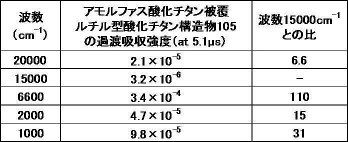
一方、被覆層を有しない従来例に係るルチル型酸化チタン構造物205は、図17に示すように、波数1000cm-1以上8000cm-1以下の波数範囲において、吸収ピークを波数5800cm-1に有する。また、ルチル型酸化チタン構造物205は、波数1000cm-1以上20000cm-1以下の波数範囲において、過渡吸収強度の最大値を波数20000cm-1に有する。ルチル型酸化チタン構造物205についても同様に、時間分解分光測定においてレーザーパルス照射の5μs後に測定した場合の波数20000cm-1、5800cm-1、2000cm-1、1000cm-1における過渡吸収強度と、波数15000cm-1における過渡吸収強度との比をそれぞれ表4に示した。
表4に示すように、ルチル型酸化チタン構造物205は、吸収ピーク(波数5800cm-1)における過渡吸収強度が、波数15000cm-1における過渡吸収強度に対し約0.43倍であることがわかる。このように、ルチル型酸化チタン構造物205は、吸収ピーク(波数5800cm-1)における過渡吸収強度に対する波数15000cm-1における過渡吸収強度の比が10倍未満であることから、光触媒活性が低いといえる。

<実験例6>
(アナターゼ型酸化チタンにおける時間分解分光測定)
図20及び21を参照して、実験例6に係るアナターゼ型酸化チタン構造物の過渡吸収スペクトルについて説明する。
(アナターゼ型酸化チタンにおける時間分解分光測定)
図20及び21を参照して、実験例6に係るアナターゼ型酸化チタン構造物の過渡吸収スペクトルについて説明する。
まず、CaF2基板上にアナターゼ型酸化チタンの薄膜を形成し、従来例に係るアナターゼ型酸化チタン構造物206とした。また、アナターゼ型酸化チタン構造物206(第1の金属化合物)の表面に、100℃の温度条件下において、厚さ2nmのアモルファス酸化チタン層(第2の金属化合物層)を原子層堆積装置により形成し、本発明に係るアナターゼ型酸化チタン構造物106を得た。アナターゼ型酸化チタン構造物106及び206について、実験例5と同様にして時間分解分光測定を行い、過渡吸収スペクトルを得た。
図20は、アナターゼ型酸化チタン構造物206の時間分解分光測定における過渡吸収スペクトルを示す図である。図21は、アナターゼ型酸化チタン構造物106の時間分解分光測定における過渡吸収スペクトルを示す図である。なお、図20において、波数6000cm-1以下の波数範囲における過渡吸収強度は、右側の縦軸を参照する。また、図21において、波数5800cm-1以下の波数範囲における過渡吸収強度は、右側の縦軸を参照する。
図20に示すように、従来例に係るアナターゼ型酸化チタン構造物206は、波数5800cm-1において自由電子又は浅くトラップされたトラップ電子による過渡吸収ピークを有する。一方、図21に示すように、表面にアモルファス酸化チタン層を有する本発明のアナターゼ型酸化チタン構造物106は、アナターゼ型酸化チタン構造物206と比較して、吸収ピークの位置に変化はないが、吸収強度が増加していることがわかる。よって、アナターゼ型酸化チタンの表面にアモルファス酸化チタン層を形成することによって、反応活性が高い電子の数が増加することがわかる。
(吸収ピークにおける過渡吸収強度の評価)
図21に示すように、アモルファス酸化チタンの被覆層を備えるアナターゼ型酸化チタン構造物106は、時間分解分光測定においてレーザーパルス照射の5μs後に測定した場合、波数1000cm-1以上20000cm-1以下の波数範囲において、過渡吸収強度の最大値を波数1000cm-1に有する。また、アナターゼ型酸化チタン構造物106は、吸収ピークを波数5800cm-1に有する。波数20000cm-1、5800cm-1、2000cm-1、1000cm-1における過渡吸収強度と、波数15000cm-1における過渡吸収強度との比をそれぞれ算出し、結果を表5に示した。
図21に示すように、アモルファス酸化チタンの被覆層を備えるアナターゼ型酸化チタン構造物106は、時間分解分光測定においてレーザーパルス照射の5μs後に測定した場合、波数1000cm-1以上20000cm-1以下の波数範囲において、過渡吸収強度の最大値を波数1000cm-1に有する。また、アナターゼ型酸化チタン構造物106は、吸収ピークを波数5800cm-1に有する。波数20000cm-1、5800cm-1、2000cm-1、1000cm-1における過渡吸収強度と、波数15000cm-1における過渡吸収強度との比をそれぞれ算出し、結果を表5に示した。
表5に示すように、アナターゼ型酸化チタン構造物106は、吸収ピーク(波数5800cm-1)における過渡吸収強度が、波数15000cm-1における過渡吸収強度に対し約25倍であることがわかる。このように、アナターゼ型酸化チタン構造物106は、吸収ピーク(波数5800cm-1)における過渡吸収強度に対する波数15000cm-1における過渡吸収強度の比が10倍以上であることから、光触媒活性が高いといえる。また、アナターゼ型酸化チタン構造物106は、過渡吸収強度が最大となる波数1000cm-1における過渡吸収強度が、波数15000cm-1における過渡吸収強度に対し約150倍であることがわかる。このことから、アナターゼ型酸化チタン構造物106は、自由電子の数が多く、光触媒活性が高いといえる。
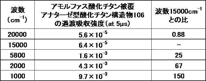
一方、被覆層を有しないアナターゼ型酸化チタン構造物206は、図20に示すように、波数1000cm-1以上8000cm-1以下の波数範囲において、吸収ピークを波数6000cm-1に有する。また、アナターゼ型酸化チタン構造物206は、波数1000cm-1以上20000cm-1以下の波数範囲において、過渡吸収強度の最大値を波数1000cm-1に有する。アナターゼ型酸化チタン構造物206についても同様に、時間分解分光測定においてレーザーパルス照射の5μs後に測定した場合の波数20000cm-1、5800cm-1、2000cm-1、1000cm-1における過渡吸収強度と、波数15000cm-1における過渡吸収強度との比をそれぞれ表6に示した。
表6に示すように、アナターゼ型酸化チタン構造物206は、吸収ピーク(波数6000cm-1)における過渡吸収強度が、波数15000cm-1における過渡吸収強度に対し約1.1倍であることがわかる。このように、アナターゼ型酸化チタン構造物206は、吸収ピーク(波数6000cm-1)における過渡吸収強度に対する波数15000cm-1における過渡吸収強度の比が10倍未満であることから、光触媒活性が低いといえる。また、アナターゼ型酸化チタン構造物206は、波数1000cm-1における過渡吸収強度が、波数15000cm-1における過渡吸収強度に対し約5.0倍であることがわかる。このことから、アナターゼ型酸化チタン構造物206は、自由電子の数が少なく、光触媒活性が低いといえる。
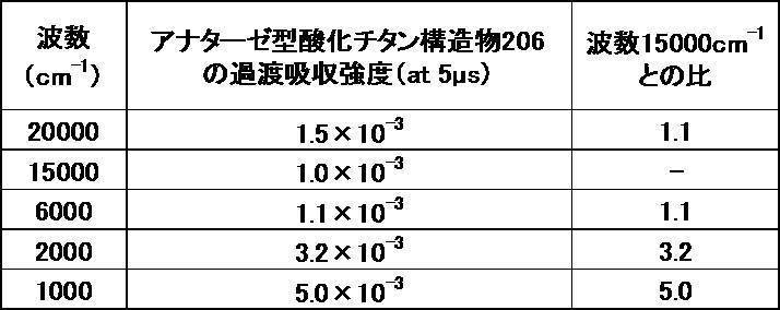
[比較例]
次に、図22及び23を参照して、比較例に係る構造物の製造方法について説明する。比較例に係る構造物の製造方法は、第1の実施形態に係る構造物100の製造方法と比較して、被覆層の形成方法が異なっている。第1の実施形態に係る構造物100において、被覆層2は、原子層堆積装置を用いて形成されるのに対し、比較例に係る構造物においては、ゾルゲル法により被覆層が形成される。
次に、図22及び23を参照して、比較例に係る構造物の製造方法について説明する。比較例に係る構造物の製造方法は、第1の実施形態に係る構造物100の製造方法と比較して、被覆層の形成方法が異なっている。第1の実施形態に係る構造物100において、被覆層2は、原子層堆積装置を用いて形成されるのに対し、比較例に係る構造物においては、ゾルゲル法により被覆層が形成される。
<実験例7>
(ゾルゲル法による被覆層の形成)
FTOガラス基板上にルチル型酸化チタン及びアナターゼ型酸化チタンを固定し、ルチル型酸化チタン電極207a及びアナターゼ型酸化チタン電極207bを得た。それぞれ酸化チタン濃度に換算して200g/Lのイソプロピルアルコール分散液100mLを調整した。別に、酸化チタン濃度に換算して10g/Lのチタンテトライソプロポキシド・イソプロピルアルコール分散液を調整し、先の酸化チタンのイソプロピルアルコール分散液に添加し、2時間撹拌後、純水を0.225g添加し、30分熟成後、溶剤を蒸発させ、アモルファス表面処理されたルチル型酸化チタン電極107a及びアナターゼ型酸化チタン電極107bを得た。このようにして得られたアモルファス表面処理酸化チタン電極107a及び107bにおける被覆層の厚さは、それぞれ90nm及び50nmであった。
(ゾルゲル法による被覆層の形成)
FTOガラス基板上にルチル型酸化チタン及びアナターゼ型酸化チタンを固定し、ルチル型酸化チタン電極207a及びアナターゼ型酸化チタン電極207bを得た。それぞれ酸化チタン濃度に換算して200g/Lのイソプロピルアルコール分散液100mLを調整した。別に、酸化チタン濃度に換算して10g/Lのチタンテトライソプロポキシド・イソプロピルアルコール分散液を調整し、先の酸化チタンのイソプロピルアルコール分散液に添加し、2時間撹拌後、純水を0.225g添加し、30分熟成後、溶剤を蒸発させ、アモルファス表面処理されたルチル型酸化チタン電極107a及びアナターゼ型酸化チタン電極107bを得た。このようにして得られたアモルファス表面処理酸化チタン電極107a及び107bにおける被覆層の厚さは、それぞれ90nm及び50nmであった。
ゾルゲル法によりアモルファス表面処理されたルチル型酸化チタン電極107a及びアナターゼ型酸化チタン電極107bについて、実験例1と同様にして、水の分解活性を測定した。結果を図22及び23に示す。図22は、アモルファス表面処理されたルチル型酸化チタン107aにおける水の分解活性を示すグラフであり、図23は、アモルファス表面処理されたアナターゼ型酸化チタン107bにおける水の分解活性を示すグラフである。図22及び23において、アモルファス表面処理していない酸化チタン電極207a及び207bの水の分解活性を実線、アモルファス表面処理された酸化チタン電極107a及107bの水の分解活性を破線で示した。
図22及び23に示すように、上述のアモルファス表面処理方法で得られた酸化チタン電極107a及107bは、被覆層を有しない酸化チタン電極207a及び207bと比較して、水の分解活性が低いことがわかる。よって、実験例1、2、及び7の結果から、被覆層をゾルゲル法により形成して得られた構造物と比較して、原子層堆積装置により被覆層を形成した構造物は、水の分解活性が高く、光触媒活性が高いといえる。
(ゾルゲル法による被覆層を有する酸化チタン電極の時間分解分光測定)
図24及び25を参照して、実験例7に係る酸化チタン電極の過渡吸収スペクトルについて説明する。ゾルゲル法によりアモルファス表面処理されたルチル型酸化チタン電極107a及びアナターゼ型酸化チタン電極107bについて、実験例1と同様にして時間分解分光測定を行い、過渡吸収スペクトルを得た。それぞれ結果を図24、図25に示す。
図24及び25を参照して、実験例7に係る酸化チタン電極の過渡吸収スペクトルについて説明する。ゾルゲル法によりアモルファス表面処理されたルチル型酸化チタン電極107a及びアナターゼ型酸化チタン電極107bについて、実験例1と同様にして時間分解分光測定を行い、過渡吸収スペクトルを得た。それぞれ結果を図24、図25に示す。
図24に示すように、ゾルゲル法によりアモルファス表面処理されたルチル型酸化チタン電極107aは、表面処理されていないルチル型酸化チタン電極207a(実験例1におけるルチル型酸化チタン電極201aと同様であるため、図17参照)と比較して、全体的に過渡吸収強度が低下したことがわかる。
図25に示すように、ゾルゲル法によりアモルファス表面処理されたアナターゼ型酸化チタン電極107bは、表面処理されていないアナターゼ型酸化チタン電極207b(実験例1におけるアナターゼ型酸化チタン電極201bと同様であるため、図20参照)と比較して、全体的に過渡吸収強度が低下したことがわかる。
(吸収ピークにおける過渡吸収強度の評価)
ルチル型酸化チタン電極107aは、図24に示すように、波数1000cm-1以上8000cm-1以下の波数範囲において、吸収ピークを波数5800cm-1に有する。また、波数1000cm-1以上20000cm-1以下の波数範囲において、過渡吸収強度の最大値を波数20000cm-1に有する。レーザーパルス照射の5μs後に測定した時間分解分光測定における波数20000cm-1、5800cm-1、2000cm-1、1000cm-1における過渡吸収強度と、波数15000cm-1における過渡吸収強度との比をそれぞれ表7に示した。
ルチル型酸化チタン電極107aは、図24に示すように、波数1000cm-1以上8000cm-1以下の波数範囲において、吸収ピークを波数5800cm-1に有する。また、波数1000cm-1以上20000cm-1以下の波数範囲において、過渡吸収強度の最大値を波数20000cm-1に有する。レーザーパルス照射の5μs後に測定した時間分解分光測定における波数20000cm-1、5800cm-1、2000cm-1、1000cm-1における過渡吸収強度と、波数15000cm-1における過渡吸収強度との比をそれぞれ表7に示した。
表7に示すように、ルチル型酸化チタン電極107aは、吸収ピーク(波数5800cm-1)における過渡吸収強度が、波数15000cm-1における過渡吸収強度に対し約0.35倍であることがわかる。このように、ゾルゲル法によりアモルファス表面処理されたルチル型酸化チタン電極107aは、吸収ピーク(波数5800cm-1)における過渡吸収強度に対する波数15000cm-1における過渡吸収強度の比が10倍未満であることから、光触媒活性が低いといえる。また、ルチル型酸化チタン電極107aは、波数1000cm-1における過渡吸収強度が、波数15000cm-1における過渡吸収強度に対し約0.049倍であることがわかる。
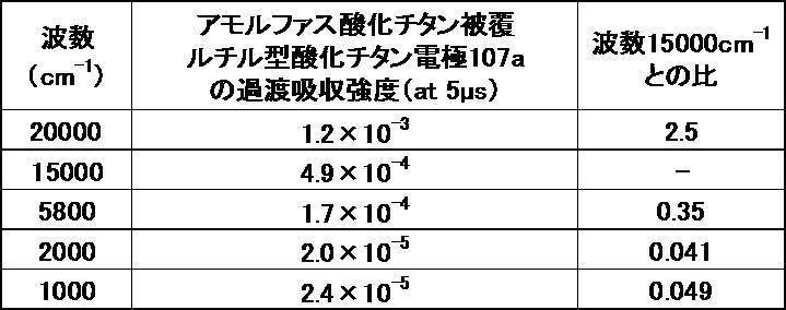
一方、アナターゼ型酸化チタン電極107bは、図25に示すように、波数20000cm-1以下の波数範囲において、過渡吸収強度の最大値を波数1000cm-1に有する。レーザーパルス照射の5μs後に測定した時間分解分光測定における波数20000cm-1、5800cm-1、2000cm-1、1000cm-1における過渡吸収強度と、波数15000cm-1における過渡吸収強度との比をそれぞれ表8に示した。
表8に示すように、アナターゼ型酸化チタン電極107bは、過渡吸収強度の最大値を示す波数1000cm-1における過渡吸収強度が、波数15000cm-1における過渡吸収強度に対し約7.3倍であることがわかる。このように、ゾルゲル法によりアモルファス表面処理されたアナターゼ型酸化チタン電極107bは、過渡吸収強度の最大値を示す波数1000cm-1における過渡吸収強度に対する波数15000cm-1における過渡吸収強度の比が10倍未満であることから、光触媒活性が低いといえる。

[変形例]
<実験例8>
(アモルファス酸化アルミニウムからなる保護層の形成:ルチル型酸化チタン)
まず、実験例1と同様にして、ルチル型酸化チタン電極208(第1の金属化合物)の表面に、被覆層として、原子層堆積装置を用いて100℃の温度条件下で厚さ4nmのアモルファス酸化チタン層(第2の金属化合物層)を形成し、本発明のルチル型酸化チタン電極108aを得た。その後、保護層として、アモルファス酸化チタン層の表面に、原子層堆積装置により、100℃の温度条件下で厚さ1nmのアモルファス酸化アルミニウム(Al2O3)層を形成し、被覆層及び保護層を備えるルチル型酸化チタン電極108bを得た。
<実験例8>
(アモルファス酸化アルミニウムからなる保護層の形成:ルチル型酸化チタン)
まず、実験例1と同様にして、ルチル型酸化チタン電極208(第1の金属化合物)の表面に、被覆層として、原子層堆積装置を用いて100℃の温度条件下で厚さ4nmのアモルファス酸化チタン層(第2の金属化合物層)を形成し、本発明のルチル型酸化チタン電極108aを得た。その後、保護層として、アモルファス酸化チタン層の表面に、原子層堆積装置により、100℃の温度条件下で厚さ1nmのアモルファス酸化アルミニウム(Al2O3)層を形成し、被覆層及び保護層を備えるルチル型酸化チタン電極108bを得た。
(水の分解における電流密度の測定:紫外線の照射)
ルチル型酸化チタン電極208、被覆層を備えるルチル型酸化チタン電極108a、被覆層及び保護層を備えるルチル型酸化チタン電極108bのそれぞれについて、以下のようにして水の分解を行い、その際に生じた電流密度を測定した。すなわち、基準電極として銀/塩化銀電極を用い、電解液として0.1MのNa2SO4水溶液を用いて、電圧を1.0Vに固定して、LEDランプ(Thorlabs社製、M375L3)を用いて波長375nmの紫外線(50mW/cm2)を連続的に照射し、水の分解を行った。紫外光の照射開始0秒~2000秒の間において電流密度を測定した。電流密度の測定は、ポテンショ・ガルバノスタット(東方技研社製、PS-14)を用いて行った。それぞれ結果を図26に示す。
ルチル型酸化チタン電極208、被覆層を備えるルチル型酸化チタン電極108a、被覆層及び保護層を備えるルチル型酸化チタン電極108bのそれぞれについて、以下のようにして水の分解を行い、その際に生じた電流密度を測定した。すなわち、基準電極として銀/塩化銀電極を用い、電解液として0.1MのNa2SO4水溶液を用いて、電圧を1.0Vに固定して、LEDランプ(Thorlabs社製、M375L3)を用いて波長375nmの紫外線(50mW/cm2)を連続的に照射し、水の分解を行った。紫外光の照射開始0秒~2000秒の間において電流密度を測定した。電流密度の測定は、ポテンショ・ガルバノスタット(東方技研社製、PS-14)を用いて行った。それぞれ結果を図26に示す。
図26に示すように、被覆層及び保護層を備えるルチル型酸化チタン電極108bは、被覆層のみを備えるルチル型酸化チタン電極108aと比較して、電流密度が大きく、減衰も緩やかであり耐久性に優れていた。このことから、アモルファス酸化アルミニウムの保護層は、アモルファス酸化チタンの被覆層を保護することにより触媒活性をさらに向上させる効果があると考えられる。
(アモルファス酸化アルミニウムからなる被覆層の形成)
ルチル型酸化チタン電極208(第1の金属化合物)の表面に、原子層堆積装置により、100℃の温度条件下で厚さ4nmのアモルファス酸化アルミニウム層(第2の金属化合物層)を形成し、ルチル型酸化チタン電極108cを得た。ルチル型酸化チタン電極108cについても同様に、紫外線を照射して水の分解を行い、電流密度を測定した。結果を図27に示す。
ルチル型酸化チタン電極208(第1の金属化合物)の表面に、原子層堆積装置により、100℃の温度条件下で厚さ4nmのアモルファス酸化アルミニウム層(第2の金属化合物層)を形成し、ルチル型酸化チタン電極108cを得た。ルチル型酸化チタン電極108cについても同様に、紫外線を照射して水の分解を行い、電流密度を測定した。結果を図27に示す。
図27に示すように、アモルファス酸化アルミニウム層を備えるルチル型酸化チタン電極108cは、ルチル型酸化チタン電極208と比較して、電流密度が同等であり、活性が維持されていたことがわかる。
(水の分解における電流密度の測定:可視光の照射)
ルチル型酸化チタン電極208、被覆層を備えるルチル型酸化チタン電極108a、被覆層及び保護層を備えるルチル型酸化チタン電極108b、アモルファス酸化アルミニウムの被覆層を備えるルチル型酸化チタン電極108cのそれぞれについて、基準電極として銀/塩化銀電極を用い、電解液として0.1MのNa2SO4水溶液を用いて、LEDランプ(Thorlabs社製、M455L3)を用いて、波長455nmの可視光を断続的に照射(200mW/cm2)して水の分解を行い、電流密度を測定して水の分解活性について評価を行った。電流密度の測定は、ポテンショ・ガルバノスタット(東方技研社製、PS-14)を用いて行った。それぞれ結果を図30に示した。
ルチル型酸化チタン電極208、被覆層を備えるルチル型酸化チタン電極108a、被覆層及び保護層を備えるルチル型酸化チタン電極108b、アモルファス酸化アルミニウムの被覆層を備えるルチル型酸化チタン電極108cのそれぞれについて、基準電極として銀/塩化銀電極を用い、電解液として0.1MのNa2SO4水溶液を用いて、LEDランプ(Thorlabs社製、M455L3)を用いて、波長455nmの可視光を断続的に照射(200mW/cm2)して水の分解を行い、電流密度を測定して水の分解活性について評価を行った。電流密度の測定は、ポテンショ・ガルバノスタット(東方技研社製、PS-14)を用いて行った。それぞれ結果を図30に示した。
図30に示すように、被覆層及び保護層を備えるルチル型酸化チタン電極108bは、可視光の照射によって高い触媒活性を発現することがわかる。また、ルチル型酸化チタン電極108bは、ルチル型酸化チタン電極108aと比較して電流密度が高かったことから、被覆層の表面に保護層を備えることにより、より触媒活性が向上することがわかる。
(吸収スペクトル)
ルチル型酸化チタン電極208、被覆層を備えるルチル型酸化チタン電極108a、被覆層及び保護層を備えるルチル型酸化チタン電極108b、アモルファス酸化アルミニウムの被覆層を備えるルチル型酸化チタン電極108cのそれぞれについて、吸収スペクトルを測定した。吸収スペクトルの測定は、紫外可視分光装置(日本分光株式会社製、V-670)に積分球(日本分光株式会社製、PIN-757)を設置し、反射配置により行った。結果を図31に示す。
ルチル型酸化チタン電極208、被覆層を備えるルチル型酸化チタン電極108a、被覆層及び保護層を備えるルチル型酸化チタン電極108b、アモルファス酸化アルミニウムの被覆層を備えるルチル型酸化チタン電極108cのそれぞれについて、吸収スペクトルを測定した。吸収スペクトルの測定は、紫外可視分光装置(日本分光株式会社製、V-670)に積分球(日本分光株式会社製、PIN-757)を設置し、反射配置により行った。結果を図31に示す。
図31に示すように、被覆層及び保護層を備えるルチル型酸化チタン電極108bは、可視光領域に吸収が出現しており、可視光の照射により光触媒活性を発現することがわかる。また、ルチル型酸化チタン電極108bは、ルチル型酸化チタン電極108aと比較して全体的に吸収強度が高いことから、アモルファス酸化アルミニウムの保護層を有することにより、より高い触媒活性が得られることがわかる。
また、図30及び図31に示すように、アモルファス酸化チタンの被覆層を備えるルチル型酸化チタン電極108aは、アモルファス酸化アルミニウムの被覆層を備えるルチル型酸化チタン電極108cと比較して、触媒活性が高くなっている。このことから、被覆層として、その金属カチオンの価数が、光触媒の金属カチオンの価数と同等以下であることで、活性が向上しやすくなることがわかる。
<実験例9>
(アモルファス酸化アルミニウムからなる保護層の形成:アナターゼ型酸化チタン)
まず、実験例1と同様にして、アナターゼ型酸化チタン電極209(第1の金属化合物)の表面に、被覆層として、原子層堆積装置を用いて100℃の温度条件下で厚さ4nmのアモルファス酸化チタン層(第2の金属化合物層)を形成し、本発明に係るアナターゼ型酸化チタン電極109aを得た。その後、保護層として、アモルファス酸化チタン層の表面に、原子層堆積装置を用いて100℃の温度条件下で厚さ1nmのアモルファス酸化アルミニウム(Al2O3)層を形成し、被覆層及び保護層を備えるアナターゼ型酸化チタン電極109bを得た。
(アモルファス酸化アルミニウムからなる保護層の形成:アナターゼ型酸化チタン)
まず、実験例1と同様にして、アナターゼ型酸化チタン電極209(第1の金属化合物)の表面に、被覆層として、原子層堆積装置を用いて100℃の温度条件下で厚さ4nmのアモルファス酸化チタン層(第2の金属化合物層)を形成し、本発明に係るアナターゼ型酸化チタン電極109aを得た。その後、保護層として、アモルファス酸化チタン層の表面に、原子層堆積装置を用いて100℃の温度条件下で厚さ1nmのアモルファス酸化アルミニウム(Al2O3)層を形成し、被覆層及び保護層を備えるアナターゼ型酸化チタン電極109bを得た。
(水の分解における電流密度の測定:紫外線の照射)
アナターゼ型酸化チタン電極209、被覆層を備えるアナターゼ型酸化チタン電極109a、被覆層及び保護層を備えるアナターゼ型酸化チタン電極109bについて、実験例8と同様にして、波長375nmの紫外線を連続的に照射して水の分解を行い、電流密度を測定した。それぞれ結果を図28に示す。
アナターゼ型酸化チタン電極209、被覆層を備えるアナターゼ型酸化チタン電極109a、被覆層及び保護層を備えるアナターゼ型酸化チタン電極109bについて、実験例8と同様にして、波長375nmの紫外線を連続的に照射して水の分解を行い、電流密度を測定した。それぞれ結果を図28に示す。
図28に示すように、被覆層及び保護層を備えるアナターゼ型酸化チタン電極109bは、被覆層のみを備えるアナターゼ型酸化チタン電極109aと比較して、電流密度の減衰が緩やかであり耐久性に優れていた。このことから、アモルファス酸化アルミニウムの保護層は、アモルファス酸化チタンの被覆層を保護することにより触媒活性をさらに向上させる効果があると考えられる。
(アモルファス酸化アルミニウムからなる被覆層の形成)
まず、アナターゼ型酸化チタン電極209(第1の金属化合物)の表面に、原子層堆積装置により、100℃の温度条件下で厚さ4nmのアモルファス酸化アルミニウム層(第2の金属化合物層)を形成し、本発明に係るアナターゼ型酸化チタン電極109cを得た。アナターゼ型酸化チタン電極109cについて、実験例8と同様にして、紫外線を照射して水の分解を行い、電流密度を測定した。結果を図29に示す。
まず、アナターゼ型酸化チタン電極209(第1の金属化合物)の表面に、原子層堆積装置により、100℃の温度条件下で厚さ4nmのアモルファス酸化アルミニウム層(第2の金属化合物層)を形成し、本発明に係るアナターゼ型酸化チタン電極109cを得た。アナターゼ型酸化チタン電極109cについて、実験例8と同様にして、紫外線を照射して水の分解を行い、電流密度を測定した。結果を図29に示す。
図29に示すように、アモルファス酸化アルミニウム層を備えるアナターゼ型酸化チタン電極109cは、アナターゼ型酸化チタン電極209と比較して、電流密度が大きく、活性が向上したことがわかる。
(水の分解における電流密度の測定:可視光の照射)
アナターゼ型酸化チタン電極209、被覆層を備えるアナターゼ型酸化チタン電極109a、被覆層及び保護層を備えるアナターゼ型酸化チタン電極109b、アモルファス酸化アルミニウムの被覆層を備えるアナターゼ型酸化チタン電極109cについて、実験例8と同様にして、波長455nmの可視光を断続的に照射して水の分解を行い、電流密度を測定した。それぞれ結果を図32に示した。
アナターゼ型酸化チタン電極209、被覆層を備えるアナターゼ型酸化チタン電極109a、被覆層及び保護層を備えるアナターゼ型酸化チタン電極109b、アモルファス酸化アルミニウムの被覆層を備えるアナターゼ型酸化チタン電極109cについて、実験例8と同様にして、波長455nmの可視光を断続的に照射して水の分解を行い、電流密度を測定した。それぞれ結果を図32に示した。
図32に示すように、被覆層及び保護層を備えるアナターゼ型酸化チタン電極109bは、可視光の照射によって高い触媒活性を発現することがわかる。また、アナターゼ型酸化チタン電極109bは、アナターゼ型酸化チタン電極109aと比較して電流密度が高かったことから、被覆層の表面に保護層を備えることにより、より触媒活性が向上することがわかる。
(吸収スペクトル)
アナターゼ型酸化チタン電極209、被覆層を備えるアナターゼ型酸化チタン電極109a、被覆層及び保護層を備えるアナターゼ型酸化チタン電極109b、アモルファス酸化アルミニウムの被覆層を備えるアナターゼ型酸化チタン電極109cについて、実験例8と同様にして、吸収スペクトルを測定した。結果を図33に示す。
アナターゼ型酸化チタン電極209、被覆層を備えるアナターゼ型酸化チタン電極109a、被覆層及び保護層を備えるアナターゼ型酸化チタン電極109b、アモルファス酸化アルミニウムの被覆層を備えるアナターゼ型酸化チタン電極109cについて、実験例8と同様にして、吸収スペクトルを測定した。結果を図33に示す。
図33に示すように、被覆層及び保護層を備えるアナターゼ型酸化チタン電極109bは、可視光領域に吸収が出現しており、可視光の照射により光触媒活性を発現することがわかる。また、アナターゼ型酸化チタン電極109bは、アナターゼ型酸化チタン電極109aと比較して全体的に吸収強度が高いことから、アモルファス酸化アルミニウムの保護層を有することにより、より高い触媒活性が得られることがわかる。
また、図32及び図33に示すように、アモルファス酸化チタンの被覆層を備えるアナターゼ型酸化チタン電極109aは、アモルファス酸化アルミニウムの被覆層を備えるアナターゼ型酸化チタン電極109cと比較して、触媒活性が高くなっている。このことから、被覆層として、その金属カチオンの価数が、光触媒の金属カチオンの価数と同等以下であることで、活性が向上しやすくなることがわかる。
<実験例10>
(被覆層形成後にアニール処理の実施:アナターゼ型酸化チタン)
図34を参照して、実験例10に係るアナターゼ型酸化チタン電極110a~110eについて説明する。まず、実験例1と同様にして、アナターゼ型酸化チタン(第1の金属化合物)の表面に、原子層堆積装置を用いて厚さ4nmのアモルファス酸化チタンの被覆層(第2の金属化合物層)を形成し、本発明に係るアナターゼ型酸化チタン電極110aを得た。被覆層を形成後、200℃の温度条件で、大気中で1時間アニール処理を行い、アナターゼ型酸化チタン電極110bを得た。また、アニール処理の温度を300℃、400℃、500℃に変更したこと以外はアナターゼ型酸化チタン電極110bと同様にして、アナターゼ型酸化チタン電極110c~110eを作製した。
(被覆層形成後にアニール処理の実施:アナターゼ型酸化チタン)
図34を参照して、実験例10に係るアナターゼ型酸化チタン電極110a~110eについて説明する。まず、実験例1と同様にして、アナターゼ型酸化チタン(第1の金属化合物)の表面に、原子層堆積装置を用いて厚さ4nmのアモルファス酸化チタンの被覆層(第2の金属化合物層)を形成し、本発明に係るアナターゼ型酸化チタン電極110aを得た。被覆層を形成後、200℃の温度条件で、大気中で1時間アニール処理を行い、アナターゼ型酸化チタン電極110bを得た。また、アニール処理の温度を300℃、400℃、500℃に変更したこと以外はアナターゼ型酸化チタン電極110bと同様にして、アナターゼ型酸化チタン電極110c~110eを作製した。
(水の分解における電流密度の測定)
アナターゼ型酸化チタン電極110a~110eのそれぞれについて、基準電極として銀/塩化銀電極、電解液として0.1MのNa2SO4水溶液を用い、LEDランプ(Thorlabs社製、M375L3)を用いて375nmの紫外線を0.1Hzで断続的に照射して(50mW/cm2)水の分解を行い、電流密度を測定して水の分解活性について評価を行った。電流密度の測定は、ポテンショ・ガルバノスタット(東方技研社製、PS-14)を用いて、印加電位を基準電極に対して-0.8Vから1.0Vまで10mV/sの速度で変化させながら水の酸化による酸化電流を測定することにより行った。結果を図34に示す。
アナターゼ型酸化チタン電極110a~110eのそれぞれについて、基準電極として銀/塩化銀電極、電解液として0.1MのNa2SO4水溶液を用い、LEDランプ(Thorlabs社製、M375L3)を用いて375nmの紫外線を0.1Hzで断続的に照射して(50mW/cm2)水の分解を行い、電流密度を測定して水の分解活性について評価を行った。電流密度の測定は、ポテンショ・ガルバノスタット(東方技研社製、PS-14)を用いて、印加電位を基準電極に対して-0.8Vから1.0Vまで10mV/sの速度で変化させながら水の酸化による酸化電流を測定することにより行った。結果を図34に示す。
図34に示すように、被覆層の形成後にアニール処理を行ったアナターゼ型酸化チタン電極110b~110eは、アニール処理を行わなかったアナターゼ型酸化チタン電極110aと比較して、電流密度が小さかったことから、触媒活性が低下することがわかる。
<実験例11>
(被覆層形成後にアニール処理の実施:ルチル型酸化チタン)
図35を参照して、実験例11に係るルチル型酸化チタン電極111a~111eについて説明する。まず、実験例1と同様にして、ルチル型酸化チタン(第1の金属化合物)の表面に、原子層堆積装置を用いて厚さ4nmのアモルファス酸化チタンの被覆層(第2の金属化合物層)を形成し、本発明に係るルチル型酸化チタン電極111aを得た。被覆層を形成後、200℃の温度条件で、大気中で1時間アニール処理を行い、ルチル型酸化チタン電極111bを得た。また、アニール処理の温度を300℃、400℃、500℃に変更したこと以外はルチル型酸化チタン電極111bと同様にして、ルチル型酸化チタン電極111c~111eを作製した。
(被覆層形成後にアニール処理の実施:ルチル型酸化チタン)
図35を参照して、実験例11に係るルチル型酸化チタン電極111a~111eについて説明する。まず、実験例1と同様にして、ルチル型酸化チタン(第1の金属化合物)の表面に、原子層堆積装置を用いて厚さ4nmのアモルファス酸化チタンの被覆層(第2の金属化合物層)を形成し、本発明に係るルチル型酸化チタン電極111aを得た。被覆層を形成後、200℃の温度条件で、大気中で1時間アニール処理を行い、ルチル型酸化チタン電極111bを得た。また、アニール処理の温度を300℃、400℃、500℃に変更したこと以外はルチル型酸化チタン電極111bと同様にして、ルチル型酸化チタン電極111c~111eを作製した。
(水の分解における電流密度の測定)
ルチル型酸化チタン電極111a~111eのそれぞれについて、実験例10と同様にして水の分解を行い、電流密度を測定した。結果を図35に示す。
ルチル型酸化チタン電極111a~111eのそれぞれについて、実験例10と同様にして水の分解を行い、電流密度を測定した。結果を図35に示す。
図35に示すように、被覆層の形成後にアニール処理を行ったルチル型酸化チタン電極111b~111eは、アニール処理を行わなかったルチル型酸化チタン電極111aと比較して、電流密度が小さかったことから、触媒活性が低下することがわかる。
以上、本発明のいくつかの実施形態を説明したが、これらの実施形態は、例として提示したものであり、発明の範囲を限定することは意図していない。これら新規な実施の形態は、その他の様々な形態で実施されることが可能であり、発明の要旨を逸脱しない範囲で、種々の省略、置き換え、変更を行うことができる。これら実施の形態やその変形は、発明の範囲や要旨に含まれるとともに、特許請求の範囲に記載された発明とその均等の範囲に含まれる。
100・・・構造物
1、11、12、13・・・金属化合物
2、21、22、23・・・被覆層
31、32、33・・・FTOガラス基板
1、11、12、13・・・金属化合物
2、21、22、23・・・被覆層
31、32、33・・・FTOガラス基板
Claims (16)
- 第1の結晶構造を有する第1の金属化合物と、
前記第1の金属化合物の表面に位置し、前記第1の結晶構造と異なる第2の構造を有する第2の金属化合物層と、
を備え、
表面に前記第2の金属化合物層を有する前記第1の金属化合物は、レーザーパルス照射の5μs後に測定した時間分解分光測定において、1000cm-1以上20000cm-1以下の波数範囲内における過渡吸収強度の最大値が、1000cm-1以上8000cm-1以下の波数範囲に存在し、
波数15000cm-1における過渡吸収強度に対する前記最大値の過渡吸収強度の比が10倍以上である
ことを特徴とする構造物。 - 第1の結晶構造を有する第1の金属化合物と、
前記第1の金属化合物の表面に位置し、前記第1の結晶構造と異なる第2の構造を有する第2の金属化合物層と、
を備え、
前記第2の金属化合物層は、厚さが10nm以下であり、
表面に前記第2の金属化合物層を有する前記第1の金属化合物は、時間分解分光測定において第1の波数未満の波数範囲に吸収ピークを有する
ことを特徴とする構造物。 - 前記第2の金属化合物層は、厚さが10nm以下であることを特徴とする請求項1又は2記載の構造物。
- 前記第2の金属化合物層の表面に、前記第1の結晶構造と異なる第3の構造を有する保護層をさらに備えることを特徴とする請求項1乃至3いずれか1項記載の構造物。
- 前記第2の構造がアモルファス構造であることを特徴とする請求項1乃至3いずれか1項記載の構造物。
- 前記第3の構造がアモルファス構造であることを特徴とする請求項4又は5記載の構造物。
- 前記過渡吸収強度の比が100倍以上であることを特徴とする請求項1記載の構造物。
- 前記第1の金属化合物が光触媒であることを特徴とする請求項1乃至7いずれか1項記載の構造物。
- 前記第1の金属化合物及び前記第2の金属化合物が金属酸化物、金属窒化物、金属酸窒化物、金属硫化物及び金属酸硫化物のいずれかであることを特徴とする請求項1乃至8いずれか1項記載の構造物。
- 第1の結晶構造を有する第1の金属化合物の表面に、前記第1の結晶構造と異なる第2の構造を有する第2の金属化合物層を形成する工程を備え、
前記第2の金属化合物層は、原子層堆積装置により形成され、
表面に前記第2の金属化合物層を有する前記第1の金属化合物は、レーザーパルス照射の5μs後に測定した時間分解分光測定において、1000cm-1以上20000cm-1以下の波数範囲内における過渡吸収強度の最大値が、1000cm-1以上8000cm-1以下の波数範囲に存在し、
波数15000cm-1における過渡吸収強度に対する前記最大値の過渡吸収強度の比が10倍以上である
ことを特徴とする構造物の製造方法。 - 第1の結晶構造を有する第1の金属化合物の表面に、前記第1の結晶構造と異なる第2の構造を有する第2の金属化合物層を形成する工程を備え、
表面に前記第2の金属化合物層を有する前記第1の金属化合物は、時間分解分光測定において第1の波数未満の波数範囲に吸収ピークを有し、
前記第2の金属化合物層は、原子層堆積装置により厚さが10nm以下となるように形成される
ことを特徴とする構造物の製造方法。 - 前記第2の金属化合物層は、厚さが10nm以下となるように形成されることを特徴とする請求項10又は11記載の構造物の製造方法。
- 前記第2の金属化合物層の表面に、前記第1の結晶構造と異なる第3の構造を有する保護層を形成する工程をさらに備えることを特徴とする請求項10乃至11いずれか1項記載の構造物の製造方法。
- 前記第2の構造がアモルファス構造であることを特徴とする請求項10乃至13いずれか1項記載の構造物の製造方法。
- 前記第3の構造がアモルファス構造であることを特徴とする請求項13又は14記載の構造物の製造方法。
- 前記第1の金属化合物が光触媒であることを特徴とする請求項10乃至15いずれか1項記載の構造物の製造方法。
Applications Claiming Priority (2)
| Application Number | Priority Date | Filing Date | Title |
|---|---|---|---|
| JP2017-013478 | 2017-01-27 | ||
| JP2017013478A JP2020054931A (ja) | 2017-01-27 | 2017-01-27 | 構造物及びその製造方法 |
Publications (1)
| Publication Number | Publication Date |
|---|---|
| WO2018139579A1 true WO2018139579A1 (ja) | 2018-08-02 |
Family
ID=62979507
Family Applications (1)
| Application Number | Title | Priority Date | Filing Date |
|---|---|---|---|
| PCT/JP2018/002459 Ceased WO2018139579A1 (ja) | 2017-01-27 | 2018-01-26 | 構造物及びその製造方法 |
Country Status (2)
| Country | Link |
|---|---|
| JP (1) | JP2020054931A (ja) |
| WO (1) | WO2018139579A1 (ja) |
Cited By (2)
| Publication number | Priority date | Publication date | Assignee | Title |
|---|---|---|---|---|
| JP2023539607A (ja) * | 2020-08-24 | 2023-09-15 | カウンシル・オブ・サイエンティフィック・アンド・インダストリアル・リサーチ・アン・インディアン・レジスタード・ボディ・インコーポレイテッド・アンダー・ザ・レジストレーション・オブ・ソサエティーズ・アクト・(アクト・21・オブ・1860) | 太陽光中でco2+h2oをc1酸素化物へ共変換する連続プロセスのための光触媒デバイス |
| CN118858810A (zh) * | 2024-07-16 | 2024-10-29 | 华中科技大学 | 前驱体脉冲时间测量系统及其测量方法、测量装置和原子层沉积系统 |
Citations (6)
| Publication number | Priority date | Publication date | Assignee | Title |
|---|---|---|---|---|
| JP2004205256A (ja) * | 2002-12-24 | 2004-07-22 | Kanagawa Acad Of Sci & Technol | 時間分解赤外分光法による光触媒の評価方法 |
| WO2013133338A1 (ja) * | 2012-03-08 | 2013-09-12 | 国立大学法人東京大学 | 光水分解反応用電極およびその製造方法 |
| CN103736500A (zh) * | 2013-12-23 | 2014-04-23 | 清华大学 | 一种二氧化钛/硫化镉/二氧化钛复合薄膜及其应用 |
| CN104028258A (zh) * | 2014-05-26 | 2014-09-10 | 浙江大学 | 一种具有核壳纳米结构的高效光催化剂的制备方法 |
| JP2014221438A (ja) * | 2013-05-13 | 2014-11-27 | 實野 孝久 | 光触媒体の製造方法および光触媒体 |
| JP2015200016A (ja) * | 2014-03-31 | 2015-11-12 | 富士フイルム株式会社 | 水分解用光電極、水分解装置 |
-
2017
- 2017-01-27 JP JP2017013478A patent/JP2020054931A/ja active Pending
-
2018
- 2018-01-26 WO PCT/JP2018/002459 patent/WO2018139579A1/ja not_active Ceased
Patent Citations (6)
| Publication number | Priority date | Publication date | Assignee | Title |
|---|---|---|---|---|
| JP2004205256A (ja) * | 2002-12-24 | 2004-07-22 | Kanagawa Acad Of Sci & Technol | 時間分解赤外分光法による光触媒の評価方法 |
| WO2013133338A1 (ja) * | 2012-03-08 | 2013-09-12 | 国立大学法人東京大学 | 光水分解反応用電極およびその製造方法 |
| JP2014221438A (ja) * | 2013-05-13 | 2014-11-27 | 實野 孝久 | 光触媒体の製造方法および光触媒体 |
| CN103736500A (zh) * | 2013-12-23 | 2014-04-23 | 清华大学 | 一种二氧化钛/硫化镉/二氧化钛复合薄膜及其应用 |
| JP2015200016A (ja) * | 2014-03-31 | 2015-11-12 | 富士フイルム株式会社 | 水分解用光電極、水分解装置 |
| CN104028258A (zh) * | 2014-05-26 | 2014-09-10 | 浙江大学 | 一种具有核壳纳米结构的高效光催化剂的制备方法 |
Non-Patent Citations (2)
| Title |
|---|
| RANASINGHE, C. S. K. ET AL.: "Transient Absorption Study of Photogenerated Charge Carriers in Electrochemical Systems , 118 A", 14 September 2016 (2016-09-14), pages 78, XP055531635, ISSN: 1343-9936 * |
| YAMAKATA, A. ET AL.: "Distinctive Behavior of Photogenerated Electrons and Holes in Anatase and Rutile TiO2 Powders", J. PHYS. CHEM. C, vol. 119, no. 43, 8 October 2015 (2015-10-08), pages 24538 - 24545, XP055529859 * |
Cited By (3)
| Publication number | Priority date | Publication date | Assignee | Title |
|---|---|---|---|---|
| JP2023539607A (ja) * | 2020-08-24 | 2023-09-15 | カウンシル・オブ・サイエンティフィック・アンド・インダストリアル・リサーチ・アン・インディアン・レジスタード・ボディ・インコーポレイテッド・アンダー・ザ・レジストレーション・オブ・ソサエティーズ・アクト・(アクト・21・オブ・1860) | 太陽光中でco2+h2oをc1酸素化物へ共変換する連続プロセスのための光触媒デバイス |
| JP7837953B2 (ja) | 2020-08-24 | 2026-03-31 | カウンシル・オブ・サイエンティフィック・アンド・インダストリアル・リサーチ・アン・インディアン・レジスタード・ボディ・インコーポレイテッド・アンダー・ザ・レジストレーション・オブ・ソサエティーズ・アクト・(アクト・21・オブ・1860) | 太陽光中でco2+h2oをc1酸素化物へ共変換する連続プロセスのための光触媒デバイス |
| CN118858810A (zh) * | 2024-07-16 | 2024-10-29 | 华中科技大学 | 前驱体脉冲时间测量系统及其测量方法、测量装置和原子层沉积系统 |
Also Published As
| Publication number | Publication date |
|---|---|
| JP2020054931A (ja) | 2020-04-09 |
Similar Documents
| Publication | Publication Date | Title |
|---|---|---|
| Kanda et al. | Facile synthesis and catalytic activity of MoS2/TiO2 by a photodeposition-based technique and its oxidized derivative MoO3/TiO2 with a unique photochromism | |
| Rahimnejad et al. | Enhancement of the photocatalytic efficiency of WO3 nanoparticles via hydrogen plasma treatment | |
| Yamakata et al. | Behavior and energy state of photogenerated charge carriers in single-crystalline and polycrystalline powder SrTiO3 studied by time-resolved absorption spectroscopy in the visible to mid-infrared region | |
| Paramasivam et al. | A review of photocatalysis using self‐organized TiO2 nanotubes and other ordered oxide nanostructures | |
| Hernández et al. | Photo-catalytic activity of BiVO4 thin-film electrodes for solar-driven water splitting | |
| Hou et al. | Hot electron-driven photocatalytic water splitting | |
| Wojtyła et al. | Doped graphitic carbon nitride: insights from spectroscopy and electrochemistry | |
| Cao et al. | Photocatalytic activity and photocorrosion of atomic layer deposited ZnO ultrathin films for the degradation of methylene blue | |
| Ashraf et al. | A Bifunctional 2D Interlayered β‐Cu2V2O7/Zn2V2O6 (CZVO) Heterojunction for Solar‐Driven Nonsacrificial Dye Degradation and Water Oxidation | |
| Li et al. | Unraveling the origin of visible light capture by core–shell TiO2 nanotubes | |
| Diamanti et al. | Anodic titanium oxide as immobilized photocatalyst in UV or visible light devices | |
| Liu et al. | Visible-light-responsive copper (II) borate photocatalysts with intrinsic midgap states for water splitting | |
| Monfort et al. | Photooxidative properties of various BiVO4/TiO2 layered composite films and study of their photocatalytic mechanism in pollutant degradation | |
| Nishanthi et al. | Plasmonic silver nanoparticles loaded titania nanotube arrays exhibiting enhanced photoelectrochemical and photocatalytic activities | |
| Baia et al. | TiO2/WO3/Au nanoarchitectures’ photocatalytic activity “from degradation intermediates to catalysts’ structural peculiarities” Part II: Aerogel based composites–fine details by spectroscopic means | |
| Regue et al. | TiO2 photoanodes with exposed {0 1 0} facets grown by aerosol-assisted chemical vapor deposition of a titanium oxo/alkoxy cluster | |
| Kuncewicz et al. | Rhodium-doped titania photocatalysts with two-step bandgap excitation by visible light—influence of the dopant concentration on photosensitization efficiency | |
| Smith et al. | Visible light water splitting via oxidized TiN thin films | |
| Desiré et al. | Tm-doped TiO2 and Tm2Ti2O7 pyrochlore nanoparticles: enhancing the photocatalytic activity of rutile with a pyrochlore phase | |
| Szewczyk et al. | TiO2/PDA multilayer nanocomposites with exceptionally sharp large-scale interfaces and nitrogen doping gradient | |
| Suzuki et al. | Improved photocatalytic O2 evolution on a Sillén–Aurivillius perovskite oxychloride Bi6NbWO14Cl by Rh2O3 additives and surface modifications | |
| Das et al. | Functional blocking layer of twisted tungsten oxide nanorod grown by electrochemical anodization for photoelectrochemical water splitting | |
| Aguilar et al. | TiO2 and pyrochlore Tm2Ti2O7 based semiconductor as a photoelectrode for dye-sensitized solar cells | |
| Vequizo et al. | Unfolding the impact of H2-reduction treatment in enhancing the photocatalytic activity of rutile TiO2 based on photocarriers dynamics | |
| Ali et al. | Efficient photoelectrodes from anatase TiO2 nanotube arrays decorated with particles/rods/3D microflower rutile crystals for photoelectrochemical water splitting |
Legal Events
| Date | Code | Title | Description |
|---|---|---|---|
| 121 | Ep: the epo has been informed by wipo that ep was designated in this application |
Ref document number: 18745221 Country of ref document: EP Kind code of ref document: A1 |
|
| NENP | Non-entry into the national phase |
Ref country code: DE |
|
| 122 | Ep: pct application non-entry in european phase |
Ref document number: 18745221 Country of ref document: EP Kind code of ref document: A1 |
|
| NENP | Non-entry into the national phase |
Ref country code: JP |