WO2018126841A1 - 一种焦距大幅可调的光子晶体透镜及其设计方法 - Google Patents
一种焦距大幅可调的光子晶体透镜及其设计方法 Download PDFInfo
- Publication number
- WO2018126841A1 WO2018126841A1 PCT/CN2017/115047 CN2017115047W WO2018126841A1 WO 2018126841 A1 WO2018126841 A1 WO 2018126841A1 CN 2017115047 W CN2017115047 W CN 2017115047W WO 2018126841 A1 WO2018126841 A1 WO 2018126841A1
- Authority
- WO
- WIPO (PCT)
- Prior art keywords
- photonic crystal
- frequency
- refractive index
- equal
- design method
- Prior art date
- Legal status (The legal status is an assumption and is not a legal conclusion. Google has not performed a legal analysis and makes no representation as to the accuracy of the status listed.)
- Ceased
Links
Images
Classifications
-
- G—PHYSICS
- G02—OPTICS
- G02B—OPTICAL ELEMENTS, SYSTEMS OR APPARATUS
- G02B1/00—Optical elements characterised by the material of which they are made; Optical coatings for optical elements
- G02B1/002—Optical elements characterised by the material of which they are made; Optical coatings for optical elements made of materials engineered to provide properties not available in nature, e.g. metamaterials
- G02B1/005—Optical elements characterised by the material of which they are made; Optical coatings for optical elements made of materials engineered to provide properties not available in nature, e.g. metamaterials made of photonic crystals or photonic band gap materials
-
- G—PHYSICS
- G02—OPTICS
- G02B—OPTICAL ELEMENTS, SYSTEMS OR APPARATUS
- G02B27/00—Optical systems or apparatus not provided for by any of the groups G02B1/00 - G02B26/00, G02B30/00
- G02B27/0012—Optical design, e.g. procedures, algorithms, optimisation routines
Definitions
- the invention belongs to the technical fields of optoelectronics, optical communication and the like. Specifically, it relates to a photonic crystal lens with a greatly adjustable focal length and a design method thereof.
- a photonic crystal is a dielectric material whose refractive index changes periodically in space, and it can effectively control the propagation behavior of photons. Since E. Yablonovitch and S. John proposed this concept twenty years ago, people have paid extensive attention to the application of photonic crystals. Especially in the field of optical communication technology, photonic crystal fibers, micro-resonator lasers, filters, integrated optical circuits and other photonic crystal devices have broad application prospects. The continuous improvement of semiconductor material micro-machining technology has greatly promoted the application of two-dimensional or even three-dimensional photonic crystal devices in practice. In recent years, tunable photonic crystal lenses and their applications have become the focus of attention in the industry, because optical microlenses are one of the core devices in the fields of optical wave shaping and light detection.
- the photonic crystal tunable lens continuously changes the convergence point of the monochromatic small-sized beam inside the photonic crystal by changing the external conditions. On the one hand, it is small in size and easy to integrate, and on the other hand it provides a direct method for wavefront modulation of small-sized beams.
- the prior art discloses a photonic crystal tunable lens. It uses MEMS technology to make micro-motion devices to change the lattice constant of photonic crystals to achieve the purpose of changing the characteristics of photonic crystals. Such a photonic crystal tunable lens inevitably has problems such as complicated manufacturing process and poor stability, which is disadvantageous for the application of the device in the integrated optical path.
- the low group velocity region coincides with the self-collimation region, and the frequency-sensitive self-collimation phenomenon can be realized.
- the beam behavior is also sensitive to the index of refraction, and on both sides of the self-collimation frequency, the photonic crystal can naturally act as a concave lens and a convex lens. Based on this structure, a novel photonic crystal tunable lens can be designed to effectively solve the previous problems.
- the object of the present invention is to provide a photonic crystal lens with a greatly adjustable focal length and a design method thereof, which have the advantages of simple fabrication, easy working conditions, and small area.
- the design method of the photonic crystal lens with greatly adjustable focal length is a design method of diffraction control based on the frequency sensitive self-collimation effect, and the specific steps are as follows:
- Step 1 Select a dielectric material, determine a photonic crystal structure type and structural parameters, and obtain an equal frequency map of the photonic crystal. Find frequency-sensitive self-collimation areas in the equal-frequency diagram;
- Step 2 Determine the working "phase space", that is, the range of the frequency space and the wave vector space, for the actual required operating frequency interval and the incident angle range;
- Step 3 Optimize the structural parameters and material parameters of the photonic crystal so that the curvature of the iso-frequency line is as sensitive as possible to the refractive index of the photonic crystal material (one or more), and avoid “appearing in the working phase space”.
- Frequency line degeneracy
- Step 4 According to the selected material characteristics, select a suitable method, such as electro-optic, thermo-optic, nonlinear or other physical effects, to change the refractive index of one or more photonic crystal constituent materials, thereby changing the focus point or virtual focus of the beam. s position.
- a suitable method such as electro-optic, thermo-optic, nonlinear or other physical effects
- step 1 the operation of step 1 can be referred to the prior art "photonic crystal supporting high frequency sensitivity self-collimation phenomenon and design method and application.
- Application date: 2013-11-27. Invention patent, PCT International Patent Application No.: PCT/CN2014/074280)".
- the operating frequency range described in step 2 includes all electromagnetic wave bands, such as visible light band, infrared band, terahertz band and microwave segment;
- the range of incident angles includes a normal incidence and an oblique incidence
- the range of the wave vector space is determined by the equal incident angle of the Brillouin zone and the beam width.
- the structural parameters of the photonic crystal described in the step 3 include, but are not limited to, a lattice type, a lattice constant, a filling ratio, a structural shape and a structural parameter in a single intracellular cell, and the like;
- the material parameters of the photonic crystal include, but are not limited to, a dielectric constant, a magnetic permeability constant, a refractive index, and the like of each constituent material of the photonic crystal;
- the lattice type of the photonic crystal may be a two-dimensional, three-dimensional or layered quasi-two-dimensional periodic structure including, but not limited to, a tetragonal lattice, a rectangular lattice, a triangular lattice, a close-packed, a diamond, etc. ;
- the sensitivity of the iso-frequency line curvature to the refractive index refers to the derivative of the curvature of the iso-frequency line to the refractive index of the photonic crystal material (one or more), which can be obtained by theoretical calculation or experimental The method is obtained;
- the "equal-frequency line degeneracy" means that different equal-frequency lines have the same frequency, and the degeneracy includes degeneracy of the same energy band, and includes degeneracy of different energy bands;
- the optimized self-collimation isometric line curvature sensitivity to refractive index is generally greater than ( ⁇ 0 is the beam vacuum wavelength), which is about 300 times larger than the bulk material, so that the focal length can be easily adjusted.
- the focal length of the photonic crystal lens designed by the design method of the invention is greatly adjustable.
- the refractive index changes by 0.2% the focal length can be increased by an order of magnitude, and the fabrication is simple, the working conditions are easy to reach, and the area is small.
- Such a photonic crystal lens with adjustable focal length can be widely applied to the fields of beam focusing, beam width control, and sensitive detection.
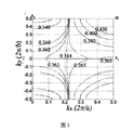
- Figure 1 shows the isospectogram of the photonic crystal structure.
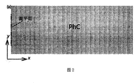
- Fig. 2 is a structural diagram showing the numerical experimental results of fine-tuning the refractive index to control the focal length.
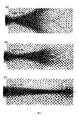
- Figure 3 is a numerical experimental result of fine-tuning the refractive index to control the focal length.
- the plane wave expansion method is used to calculate the dispersion relation of the structure, and the second band is selected and the equal-frequency diagram of the band is calculated.
- Figure 1 shows the calculation result.
- the selected working wavelength is 1.55 ⁇ m, which is widely used in optical communication band and lattice period.
- a 564 nm, using a normal incidence scheme, the beam width is 15a, and the longitudinal wave vector k y is limited to The transverse wave vector is determined by the operating wavelength.
- the refractive index of Ge is finely adjusted by the thermo-optic effect, and light is incident on the inside of the photonic crystal to produce different diffraction characteristics.
- the location of their convergence points is significantly different, indicating that the focal length of such a photonic crystal lens is adjustable.
- Such a photonic crystal lens with adjustable focal length can be widely applied to the fields of beam focusing, beam width control, and sensitive detection.
Landscapes
- Physics & Mathematics (AREA)
- General Physics & Mathematics (AREA)
- Optics & Photonics (AREA)
- Chemical & Material Sciences (AREA)
- Crystallography & Structural Chemistry (AREA)
- Optical Integrated Circuits (AREA)
- Optical Modulation, Optical Deflection, Nonlinear Optics, Optical Demodulation, Optical Logic Elements (AREA)
Abstract
一种焦距大幅可调的光子晶体透镜及其设计方法。该方法包括:初步选定光子晶体材料和结构,获得等频图,找到频率敏感自准直区域;针对实际需要工作频率区间和入射角范围,确定工作相空间;对光子晶体进行结构参数和材料参数优化设计,使得等频线曲率对光子晶体材料折射率的敏感度尽可能大,同时避免在工作相空间内出现等频线简并;根据所选材料特性,选择合适的方式,改变光子晶体组成材料的折射率,进而改变光束聚焦点或虚焦点的位置。在相同条件下,本方案所需折射率的变化比块体材料或普通光子晶体要小多个数量级,易于实现。本设计集成性好,能应用于光束调焦、光束宽度控制、敏感探测等领域。
Description
本发明属于光电子、光通信等技术领域。具体涉及一种焦距大幅可调的光子晶体透镜及其设计方法。
光子晶体是折射率在空间周期性变化的介质材料,它能够有效地控制光子的传播行为。自E.Yablonovitch和S.John在二十年前提出这一概念以来,人们就对光子晶体的应用给予广泛关注。特别是在光通信技术领域,光子晶体光纤、微谐振腔激光器、滤波器、集成光路等光子晶体器件有着广阔的应用前景。半导体材料微细加工技术的不断提高大大地推动了二维甚至三维光子晶体器件在实际中的应用步伐。近年来,可调光子晶体透镜及其应用成为了业界关注的热点,因为光学微透镜是光波整形、光探测等领域中的核心器件之一。光子晶体可调透镜通过改变外界条件,使单色小尺寸光束在光子晶体内部的会聚点连续变化。它的特点一方面是体积小易于集成,而另一方面它提供了一种直接的小尺寸光束波前调制的方法。现有文献公开了一种光子晶体可调透镜。它利用MEMS技术制作微动装置来改变光子晶体的晶格常数以达到改变光子晶体特性的目的。这种光子晶体可调透镜不可避免地存在制作工艺复杂、稳定性差等问题,不利于器件在集成光路中的应用。
通过降低晶格对称性,调节范霍夫奇异点的位置,使得低群速度区域与自准直区域重合,可以实现频率敏感的自准直现象。我们发现在这类结构中,光束行为也是对折射率敏感的,而且在自准直频率两侧,光子晶体天然地能够充当凹透镜和凸透镜。基于此结构设计新型光子晶体可调透镜,可以有效的解决之前的问题。
发明内容
本发明的目的在于提供一种焦距大幅可调的光子晶体透镜及其设计方法,使该光子晶体透镜具有制作简单、工作条件易于达到、面积小巧等优点。
本发明提供的焦距大幅可调的光子晶体透镜的设计方法,是一种基于频率敏感自准直效应的衍射调控的设计方法,具体步骤如下:
步骤1、选定介质材料,确定光子晶体结构类型和结构参数,获得该光子晶体的等频图,
在等频图中寻找频率敏感的自准直区域;
步骤2、针对实际需要工作频率区间和入射角范围,确定工作“相空间”,即频率空间和波矢空间的范围;
步骤3、对光子晶体进行结构参数和材料参数优化设计,使得等频线曲率对光子晶体材料(某种或多种)折射率的敏感度尽可能大,同时避免在工作相空间内出现“等频线简并”;
步骤4、根据所选材料特性,选择合适的方式,比如电光、热光、非线性或其他物理效应,使一种或多种光子晶体组成材料的折射率改变,进而改变光束聚焦点或虚焦点的位置。
本发明中,步骤1的操作可参见已有技术“支持高频率敏感度自准直现象的光子晶体及设计方法和应用.申请号:201310625054.2.申请日期:2013-11-27.(发明专利,PCT国际专利申请号:PCT/CN2014/074280)”。
本发明中,步骤2中所述的工作频率范围包括所有电磁波波段,如可见光波段、红外波段、太赫兹波段和微波段等;
所述的入射角范围包括正入射情况,也包括斜入射情况;
所述的波矢空间的范围是通过布里渊区的等入射角线以及光束宽度来确定。
本发明中,步骤3中所述的光子晶体的结构参数包括但不限于晶格类型、晶格常数、填充比、单原胞内的结构形状和结构参数等;
所述的光子晶体的材料参数包括但不限于光子晶体各个组成材料的介电常数、磁导率常数和折射率等;
所述的光子晶体的晶格类型,可以是二维、三维或层状准二维周期结构,包括但不限于正方晶格、长方晶格、三角晶格、密堆、金刚石等晶格结构;
所述的等频线曲率对折射率的敏感度,是指等频线曲率对光子晶体材料(某种或多种)折射率的导数,它可以用理论计算的方法得到,也可以用实验的方法得到;所述的“等频线简并”是指不同的等频线具有相同的频率,这个简并包括同一能带的简并,也包括不同能带的简并;
所述的优化后的自准直等频线曲率对折射率的敏感度,一般需要大于 (λ0为光束真空波长),大约是块体材料的300倍以上,才易实现焦距可调。
本发明设计方法设计得到的光子晶体透镜的焦距大幅可调,当折射率变化0.2%时,焦距可以增大一个数量级,并且制作简单、工作条件易于达到、面积小巧。这种焦距高度可调的光子晶体透镜能广泛应用于能应用于光束调焦、光束宽度控制、敏感探测等领域。
图1选定光子晶体结构等频图。
图2微调折射率控制焦距的数值实验结果的结构示意图。
图3微调折射率控制焦距的数值实验结果图。其中,(a)-(c)对应的微调后的Ge的折
射率分别为n1=3.988,n2=3.992,n3=3.996。
下面通过一个具体实施例来说明本发明的光子晶体透镜的设计方法,
1、选定光子晶体材料,确定材料折射率,选择光子晶体结构类型,确定结构参数:本发明具体实施例中选用材料Ge,折射率为n=4.0,这种材料的制备技术成熟。由这种介质柱构造光子晶体是由多个介质柱组成的长方晶格结构,介质柱的半径为r=0.27a,这里a是晶格周期,长宽比为1.2。并利用平面波展开法计算该结构的色散关系,选择第二个能带并计算该能带的等频图,图1为计算结果。
2、选定实际需要工作频率区间和入射角范围,确定工作“相空间”,即频率空间和波矢空间的范围:选定工作波长为1.55μm,是目前广泛应用光通信波段,晶格周期a=564nm,采用正入射方案,光束宽度为15a,纵向波矢ky限定在 横向波矢由工作波长确定。
3、计算该光子晶体的等频线曲率对折射率的敏感度,判断敏感度是否足够大以及自准直频率是否存在简并;若敏感度不够大或存在简并,则继续优化参数。此设计结构计算所得的等频线曲率对折射率的敏感度为 (λ0为光束真空波长),约为块体材料的10000倍。
4、选定光子晶体尺寸以及工作波长后,通过热光效应微调Ge的折射率,光入射到光子晶体内部会产生不同的衍射特性。图2(b)-(d)对应的微调后的Ge的折射率分别为n1=3.988,n2=3.992,n3=3.996。它们的会聚点位置有显著差别,从而说明此种光子晶体透镜的焦距高度可调。这种焦距高度可调的光子晶体透镜能广泛应用于能应用于光束调焦、光束宽度控制、敏感探测等领域。
Claims (7)
- 一种焦距大幅可调的光子晶体透镜的设计方法,其特征在于,具体步骤为:步骤1、选定介质材料,确定光子晶体结构类型和结构参数,获得该光子晶体的等频图,在等频图中寻找频率敏感的自准直区域;步骤2、针对实际需要工作频率区间和入射角范围,确定工作“相空间”,即频率空间和波矢空间的范围;步骤3、对光子晶体进行结构参数和材料参数优化设计,使得等频线曲率对光子晶体材料折射率的敏感度尽可能大,同时避免在工作相空间内出现“等频线简并”;步骤4、根据所选材料特性,选择合适的方式,包括电光、热光、非线性或其他物理效应,使一种或多种光子晶体组成材料的折射率改变,进而改变光束聚焦点或虚焦点的位置。
- 根据权利要求1所述的设计方法,其特征在于,步骤2中所述的工作频率范围为所有电磁波波段,包括可见光波段、红外波段、太赫兹波段和微波段;步骤2所述的入射角范围包括正入射情况,也包括斜入射情况;步骤2所述的波矢空间的范围是通过布里渊区的等入射角线以及光束宽度来确定。
- 根据权利要求1所述的设计方法,其特征在于,步骤3中所述的光子晶体的结构参数包括晶格类型、晶格常数、填充比、单原胞内的结构形状和结构参数;所述的光子晶体的材料参数包括光子晶体各个组成材料的介电常数、磁导率常数和折射率;所述的光子晶体的晶格类型是二维、三维或层状准二维周期结构,包括正方晶格、长方晶格、三角晶格、密堆、金刚石的晶格结构;
- 根据权利要求1所述的设计方法,其特征在于,步骤3中所述的等频线曲率对折射率的敏感度,是指等频线曲率对光子晶体材料折射率的导数,它用理论计算的方法得到,或者用实验的方法得到。
- 根据权利要求1所述的设计方法,其特征在于,步骤3中所述的“等频线简并”是指不同的等频线具有相同的频率,这个简并包括同一能带的简并,也包括不同能带的简并。
- 根据权利要求1所述的设计方法,其特征在于,步骤3中优化后的自准直等频线曲率对折射率的敏感度,需要大于λ0为光束真空波长,是块体材料的200-300倍以上。

- 由权利要求1-6之一所述的设计方法得到的焦距大幅可调的光子晶体透镜。
Applications Claiming Priority (2)
| Application Number | Priority Date | Filing Date | Title |
|---|---|---|---|
| CN201710011883.X | 2017-01-08 | ||
| CN201710011883.XA CN106842371B (zh) | 2017-01-08 | 2017-01-08 | 一种焦距大幅可调的光子晶体透镜及其设计方法 |
Publications (1)
| Publication Number | Publication Date |
|---|---|
| WO2018126841A1 true WO2018126841A1 (zh) | 2018-07-12 |
Family
ID=59117363
Family Applications (1)
| Application Number | Title | Priority Date | Filing Date |
|---|---|---|---|
| PCT/CN2017/115047 Ceased WO2018126841A1 (zh) | 2017-01-08 | 2017-12-07 | 一种焦距大幅可调的光子晶体透镜及其设计方法 |
Country Status (2)
| Country | Link |
|---|---|
| CN (1) | CN106842371B (zh) |
| WO (1) | WO2018126841A1 (zh) |
Cited By (1)
| Publication number | Priority date | Publication date | Assignee | Title |
|---|---|---|---|---|
| CN114815323A (zh) * | 2022-06-02 | 2022-07-29 | 苏州电光波工业智能科技有限公司 | 一种光子晶体调频方法和系统 |
Families Citing this family (3)
| Publication number | Priority date | Publication date | Assignee | Title |
|---|---|---|---|---|
| CN106842371B (zh) * | 2017-01-08 | 2019-05-31 | 复旦大学 | 一种焦距大幅可调的光子晶体透镜及其设计方法 |
| CN108917925B (zh) * | 2018-05-16 | 2020-06-05 | 南京大学 | 一种基于光学奇异点设计的多层膜光探测器及其探测方法 |
| CN110750005B (zh) | 2018-07-23 | 2021-04-20 | 京东方科技集团股份有限公司 | 显示装置及其显示方法 |
Citations (6)
| Publication number | Priority date | Publication date | Assignee | Title |
|---|---|---|---|---|
| CN101055400A (zh) * | 2006-12-30 | 2007-10-17 | 中国科学院上海微系统与信息技术研究所 | 可调性光子晶体自准直效应的光束调节器、方法及应用 |
| US20070297734A1 (en) * | 2006-06-23 | 2007-12-27 | Mihai Ibanescu | Efficient terahertz sources by optical rectification in photonic crystals and metamaterials exploiting tailored transverse dispersion relations |
| CN104678491A (zh) * | 2013-11-27 | 2015-06-03 | 中国科学院上海微系统与信息技术研究所 | 支持高频率敏感度自准直现象的光子晶体及设计方法和应用 |
| CN105116490A (zh) * | 2015-09-16 | 2015-12-02 | 南京邮电大学 | 一种焦距可控一维光子晶体平凹镜的设计方法 |
| CN105425504A (zh) * | 2015-12-23 | 2016-03-23 | 山东大学 | 基于自准直干涉效应的二维光子晶体逻辑或门 |
| CN106842371A (zh) * | 2017-01-08 | 2017-06-13 | 复旦大学 | 一种焦距大幅可调的光子晶体透镜及其设计方法 |
Family Cites Families (3)
| Publication number | Priority date | Publication date | Assignee | Title |
|---|---|---|---|---|
| WO2006124962A2 (en) * | 2005-05-16 | 2006-11-23 | Northeastern University | Photonic crystal devices using negative refraction |
| CN102231034B (zh) * | 2006-12-30 | 2015-06-17 | 中国科学院上海微系统与信息技术研究所 | 利用可调性光子晶体自准直效应的光束调节器及应用 |
| CN104977651B (zh) * | 2014-04-01 | 2018-05-25 | 中国科学院上海微系统与信息技术研究所 | 超高分辨率光子晶体超棱镜及其设计方法 |
-
2017
- 2017-01-08 CN CN201710011883.XA patent/CN106842371B/zh not_active Expired - Fee Related
- 2017-12-07 WO PCT/CN2017/115047 patent/WO2018126841A1/zh not_active Ceased
Patent Citations (6)
| Publication number | Priority date | Publication date | Assignee | Title |
|---|---|---|---|---|
| US20070297734A1 (en) * | 2006-06-23 | 2007-12-27 | Mihai Ibanescu | Efficient terahertz sources by optical rectification in photonic crystals and metamaterials exploiting tailored transverse dispersion relations |
| CN101055400A (zh) * | 2006-12-30 | 2007-10-17 | 中国科学院上海微系统与信息技术研究所 | 可调性光子晶体自准直效应的光束调节器、方法及应用 |
| CN104678491A (zh) * | 2013-11-27 | 2015-06-03 | 中国科学院上海微系统与信息技术研究所 | 支持高频率敏感度自准直现象的光子晶体及设计方法和应用 |
| CN105116490A (zh) * | 2015-09-16 | 2015-12-02 | 南京邮电大学 | 一种焦距可控一维光子晶体平凹镜的设计方法 |
| CN105425504A (zh) * | 2015-12-23 | 2016-03-23 | 山东大学 | 基于自准直干涉效应的二维光子晶体逻辑或门 |
| CN106842371A (zh) * | 2017-01-08 | 2017-06-13 | 复旦大学 | 一种焦距大幅可调的光子晶体透镜及其设计方法 |
Cited By (1)
| Publication number | Priority date | Publication date | Assignee | Title |
|---|---|---|---|---|
| CN114815323A (zh) * | 2022-06-02 | 2022-07-29 | 苏州电光波工业智能科技有限公司 | 一种光子晶体调频方法和系统 |
Also Published As
| Publication number | Publication date |
|---|---|
| CN106842371A (zh) | 2017-06-13 |
| CN106842371B (zh) | 2019-05-31 |
Similar Documents
| Publication | Publication Date | Title |
|---|---|---|
| Yang et al. | Active optical metasurfaces: comprehensive review on physics, mechanisms, and prospective applications | |
| WO2018126841A1 (zh) | 一种焦距大幅可调的光子晶体透镜及其设计方法 | |
| US9915832B2 (en) | Optical phased array using guided resonance with backside reflectors | |
| CN113805264B (zh) | 基于集成超颖表面的宽带消色差透镜和波束偏折器 | |
| CN109031477A (zh) | 一种全介质超表面级联的广角平面镜头制作方法 | |
| CN104749665B (zh) | 基于介质材料的平面透镜单元、平面透镜及制备方法 | |
| CN107315206A (zh) | 基于全介质超表面结构的高效红外光学透镜及其制备方法 | |
| CN113741065B (zh) | 一种旋光与极化可调的方形晶格超表面谐振器 | |
| CN112946793A (zh) | 基于介质超表面的偏振非依赖宽带消色差器件 | |
| Luo et al. | Catenary optics: a perspective of applications and challenges | |
| CN109856704A (zh) | 一种宽带消色差全介质平面透镜的制作方法 | |
| Wang et al. | Electrically and thermally tunable multifunctional terahertz metasurface array | |
| CN106772795A (zh) | 一种高效率的多频点1×3光子晶体分束器结构 | |
| CN114879282A (zh) | 一种基于介质超表面的激光防护膜及其制备方法 | |
| CN109324361B (zh) | 一种超宽波段近完美吸收器及其制造方法 | |
| CN114706151B (zh) | 一种基于仿生蛾眼结构的保偏宽谱聚焦中红外超构透镜 | |
| Murzin et al. | Redistribution of the laser beam power using diffractive optical elements | |
| CN110568524A (zh) | 一种具有低损耗的零折射率超构材料及设计方法 | |
| Zhou et al. | Sub-wavelength focusing in the visible wavelength range realized by a one-dimensional ternary photonic crystal plano-concave lens | |
| CN120595407A (zh) | 一种十字结构双层介质宽带消色差超透镜设计 | |
| Fang et al. | Highly efficient beam control of transmitted terahertz wave based on all dielectric encoding metasurface | |
| Jiang et al. | Broadband and wide angle perfect reflection by super periodic cubes metamaterials in terahertz region | |
| CN216561062U (zh) | 一种基于超表面的轻小型相机 | |
| CN111323874A (zh) | 一种复合结构光子晶体波分复用器件及其使用方法 | |
| Feng et al. | Designing Dielectric-Metalens with Selection of Structural Units Encircling an Exceptional Point |
Legal Events
| Date | Code | Title | Description |
|---|---|---|---|
| 121 | Ep: the epo has been informed by wipo that ep was designated in this application |
Ref document number: 17890302 Country of ref document: EP Kind code of ref document: A1 |
|
| NENP | Non-entry into the national phase |
Ref country code: DE |
|
| 122 | Ep: pct application non-entry in european phase |
Ref document number: 17890302 Country of ref document: EP Kind code of ref document: A1 |