WO2018123730A1 - Audio reproduction device - Google Patents
Audio reproduction device Download PDFInfo
- Publication number
- WO2018123730A1 WO2018123730A1 PCT/JP2017/045521 JP2017045521W WO2018123730A1 WO 2018123730 A1 WO2018123730 A1 WO 2018123730A1 JP 2017045521 W JP2017045521 W JP 2017045521W WO 2018123730 A1 WO2018123730 A1 WO 2018123730A1
- Authority
- WO
- WIPO (PCT)
- Prior art keywords
- piezoelectric
- signal
- piezoelectric element
- audio
- resistor
- Prior art date
Links
- 230000005236 sound signal Effects 0.000 claims abstract description 29
- 239000003990 capacitor Substances 0.000 claims abstract description 26
- 230000003321 amplification Effects 0.000 claims abstract description 5
- 238000003199 nucleic acid amplification method Methods 0.000 claims abstract description 5
- 230000004888 barrier function Effects 0.000 claims description 6
- 238000010586 diagram Methods 0.000 description 13
- 239000002184 metal Substances 0.000 description 10
- 229910052751 metal Inorganic materials 0.000 description 10
- 230000007774 longterm Effects 0.000 description 4
- 239000000919 ceramic Substances 0.000 description 3
- 230000004048 modification Effects 0.000 description 3
- 238000012986 modification Methods 0.000 description 3
- 239000000758 substrate Substances 0.000 description 3
- PXHVJJICTQNCMI-UHFFFAOYSA-N Nickel Chemical compound [Ni] PXHVJJICTQNCMI-UHFFFAOYSA-N 0.000 description 2
- 230000002238 attenuated effect Effects 0.000 description 2
- 230000000694 effects Effects 0.000 description 2
- 230000006870 function Effects 0.000 description 2
- 230000020169 heat generation Effects 0.000 description 2
- 239000000463 material Substances 0.000 description 2
- 238000001228 spectrum Methods 0.000 description 2
- 229910001369 Brass Inorganic materials 0.000 description 1
- WQZGKKKJIJFFOK-GASJEMHNSA-N Glucose Natural products OC[C@H]1OC(O)[C@H](O)[C@@H](O)[C@@H]1O WQZGKKKJIJFFOK-GASJEMHNSA-N 0.000 description 1
- 239000008280 blood Substances 0.000 description 1
- 210000004369 blood Anatomy 0.000 description 1
- 239000010951 brass Substances 0.000 description 1
- 239000002131 composite material Substances 0.000 description 1
- 238000010276 construction Methods 0.000 description 1
- 230000007423 decrease Effects 0.000 description 1
- 230000005669 field effect Effects 0.000 description 1
- 239000008103 glucose Substances 0.000 description 1
- 230000036541 health Effects 0.000 description 1
- 230000017525 heat dissipation Effects 0.000 description 1
- 230000010354 integration Effects 0.000 description 1
- 229910052759 nickel Inorganic materials 0.000 description 1
- 238000005070 sampling Methods 0.000 description 1
- 229920006395 saturated elastomer Polymers 0.000 description 1
Images


Classifications
-
- G—PHYSICS
- G10—MUSICAL INSTRUMENTS; ACOUSTICS
- G10K—SOUND-PRODUCING DEVICES; METHODS OR DEVICES FOR PROTECTING AGAINST, OR FOR DAMPING, NOISE OR OTHER ACOUSTIC WAVES IN GENERAL; ACOUSTICS NOT OTHERWISE PROVIDED FOR
- G10K9/00—Devices in which sound is produced by vibrating a diaphragm or analogous element, e.g. fog horns, vehicle hooters or buzzers
- G10K9/12—Devices in which sound is produced by vibrating a diaphragm or analogous element, e.g. fog horns, vehicle hooters or buzzers electrically operated
- G10K9/122—Devices in which sound is produced by vibrating a diaphragm or analogous element, e.g. fog horns, vehicle hooters or buzzers electrically operated using piezoelectric driving means
-
- H—ELECTRICITY
- H04—ELECTRIC COMMUNICATION TECHNIQUE
- H04R—LOUDSPEAKERS, MICROPHONES, GRAMOPHONE PICK-UPS OR LIKE ACOUSTIC ELECTROMECHANICAL TRANSDUCERS; DEAF-AID SETS; PUBLIC ADDRESS SYSTEMS
- H04R17/00—Piezoelectric transducers; Electrostrictive transducers
-
- H—ELECTRICITY
- H04—ELECTRIC COMMUNICATION TECHNIQUE
- H04R—LOUDSPEAKERS, MICROPHONES, GRAMOPHONE PICK-UPS OR LIKE ACOUSTIC ELECTROMECHANICAL TRANSDUCERS; DEAF-AID SETS; PUBLIC ADDRESS SYSTEMS
- H04R3/00—Circuits for transducers, loudspeakers or microphones
Abstract
[Problem] To provide: a piezoelectric buzzer that is inexpensive, has high-quality sound, and is low in current consumption; and an audio reproduction device that reproduces audio using said piezoelectric buzzer. [Solution] The present invention is provided with: a piezoelectric buzzer 60 having a piezoelectric element PZ that outputs, in the form of audio, vibration generated from a piezoelectric body 61 as a result of applying a signal voltage to the piezoelectric body 61, and having a resistor 65 (R0) that is connected in series to the piezoelectric element PZ and that constitutes a low-pass filter in conjunction with a capacitor equivalent to the piezoelectric element PZ; a microcomputer 20C which generates a PWM signal corresponding to an audio signal; and a drive circuit 20C in which power amplification is carried out by a switching operation performed, on the basis of the PWM signal, by four bipolar transistors constituting an H-bridge circuit 20C and which outputs a signal voltage of low consumption current corresponding to the PWM signal to the piezoelectric buzzer 60, in which the piezoelectric element 61 and the resistor 65 having a resistance value appropriate for the characteristic of the piezoelectric element 61 are connected in series, so as to generate an audio output of the piezoelectric buzzer 60.
Description
本発明は、圧電体に信号電圧を加えることで圧電体が歪み、その圧電体の振動を音声として出力する圧電ブザー、及びその圧電ブザーを用いて音声を再生する音声再生装置に関する。
The present invention relates to a piezoelectric buzzer that distorts a piezoelectric body by applying a signal voltage to the piezoelectric body and outputs the vibration of the piezoelectric body as sound, and an audio reproducing apparatus that reproduces sound using the piezoelectric buzzer.
圧電ブザー(圧電スピーカー、ピエゾメーカー、圧電サウンダーともいう。)は、小型で消費電力が少ないことから、電子ブザーなどの発音デバイス(発音部品)として用いられている。圧電ブザーは、特定周波数のSin波や矩形波を出力するように電気的・音響的に設計されている。
Piezoelectric buzzers (also called piezoelectric speakers, piezo makers, and piezoelectric sounders) are small and have low power consumption, so they are used as sounding devices (sounding parts) such as electronic buzzers. The piezoelectric buzzer is electrically and acoustically designed to output a sine wave or a rectangular wave having a specific frequency.
圧電ブザーから音楽や人の声を出力する場合、次のような問題が存在する。まず、圧電ブザーは、特定周波数の音声出力しか想定していないため、共振を利用して特定周波数の音を高い音圧で出力するように設計されている。このように、圧電ブザーは特定周波数の音声出力に適した設計であるので、圧電ブザーから出力する音楽や人の声は実用的な音質にならない(つまり音質が悪い)。また、圧電ブザーの電気的特性は、基本的コンデンサ(キャパシタ)であるので、圧電ブザーから出力する音の周波数が上がるほど消費電流が増える。特に圧電ブザーをフィルタレスD級アンプで駆動する場合、矩形波に含まれる高調波成分によって消費電流が増大する。そのため、圧電ブザーには可聴帯以外の周波数成分を抑圧するためのフィルタが必要となる。
When outputting music and human voice from a piezoelectric buzzer, the following problems exist. First, since the piezoelectric buzzer assumes only a sound output of a specific frequency, the piezoelectric buzzer is designed to output a sound of a specific frequency with a high sound pressure using resonance. As described above, since the piezoelectric buzzer is designed for sound output of a specific frequency, music and human voice output from the piezoelectric buzzer do not have practical sound quality (that is, sound quality is poor). In addition, since the electrical characteristic of the piezoelectric buzzer is a basic capacitor (capacitor), the current consumption increases as the frequency of the sound output from the piezoelectric buzzer increases. In particular, when the piezoelectric buzzer is driven by a filterless class D amplifier, current consumption increases due to harmonic components included in the rectangular wave. For this reason, the piezoelectric buzzer needs a filter for suppressing frequency components other than the audible band.
例えば、下記特許文献1には、所定の周波数成分をカットするローパスフィルタを備えたD級アンプが開示されている。このD級アンプは、ピエゾスピーカー(圧電素子)と直列にコイル(インダクタ)と抵抗が接続されている(図10参照)。そして、ピエゾスピーカーはコンデンサ(キャパシタ)と等価であり、ピエゾスピーカーとコイルとでローパスフィルタであるLCフィルタ(2次フィルタ)を構成している。抵抗はLCフィルタの共振を抑制するために設けられている。
For example, Patent Document 1 below discloses a class D amplifier including a low-pass filter that cuts a predetermined frequency component. In this class D amplifier, a coil (inductor) and a resistor are connected in series with a piezo speaker (piezoelectric element) (see FIG. 10). The piezo speaker is equivalent to a capacitor (capacitor), and the piezo speaker and the coil constitute an LC filter (secondary filter) that is a low-pass filter. The resistor is provided to suppress the resonance of the LC filter.
また、下記特許文献2には、圧電ブザー(圧電素子)に音量調整用の抵抗が接続された構成の制御回路が開示されている。ただし、圧電ブザーに接続された抵抗は、音量調整用であって、フィルタを構成するものではない。
Also, Patent Document 2 below discloses a control circuit having a configuration in which a volume adjusting resistor is connected to a piezoelectric buzzer (piezoelectric element). However, the resistor connected to the piezoelectric buzzer is for volume adjustment and does not constitute a filter.
しかしながら、特許文献1に記載された構成では、ピエゾスピーカー(圧電素子)とコイルとでLCフィルタを構成しているので、RCフィルタを構成する場合と比較して価格が高くなってしまう。また、特許文献2に記載された構成では、圧電ブザー(圧電素子)に接続された抵抗はブザーの音量を調整するために設けられたものであって、ブザーの音質を改善するためのRCフィルタを構成するものではない。
However, in the configuration described in Patent Document 1, since the LC filter is configured by the piezo speaker (piezoelectric element) and the coil, the price is higher than that in the case of configuring the RC filter. In the configuration described in Patent Document 2, the resistor connected to the piezoelectric buzzer (piezoelectric element) is provided for adjusting the volume of the buzzer, and an RC filter for improving the sound quality of the buzzer. It does not constitute.
また、フィルタを設けることなく、PWM信号(PWM:Pulse Width Modulation、パルス幅変調)で駆動される駆動回路(例えばHブリッジ回路)に直接、圧電素子を取り付けて音声出力を行う場合、圧電素子の容量が瞬間的にチャージされ圧電素子が飽和してしまうという問題が生じる。また、この場合、PWM信号の基本波である矩形波の基本周波数成分と高調波成分のエネルギーが消費され、音声再生装置全体の消費電力が増大してしまうという問題も生じる。
In addition, when an audio output is performed by directly attaching a piezoelectric element to a drive circuit (for example, an H bridge circuit) driven by a PWM signal (PWM: Pulse Width Modulation, pulse width modulation) without providing a filter, There arises a problem that the capacitance is instantaneously charged and the piezoelectric element is saturated. Further, in this case, the energy of the fundamental frequency component and the harmonic component of the rectangular wave that is the fundamental wave of the PWM signal is consumed, resulting in a problem that the power consumption of the entire audio reproduction device increases.
本発明は、前述した事情に鑑みてなされたものであり、外付けのローパスフィルタを設けることなく、安価で、高音質かつ低消費電流の音声再生装置を提供することを目的とする。
The present invention has been made in view of the above-described circumstances, and an object thereof is to provide an audio reproduction device that is inexpensive, has high sound quality, and consumes low current without providing an external low-pass filter.
上記目的を達成するために、本発明では、圧電体に信号電圧を加えることで発生する圧電体の振動を音声として出力する、共振を利用して特定周波数の音声出力に適した圧電素子と、圧電素子に直列に接続され、圧電素子と等価であるキャパシタとともにローパスフィルタを構成する抵抗とを有し、別途のローパスフィルタを用いずに周波数成分を抑圧する圧電ブザーと、ミドルウェアに基づいて、音声信号に応じたPWM信号を生成するマイクロコンピュータと、マイクロコンピュータで生成されるPWM信号に基づいて、Hブリッジ回路を構成する4つのバイポーラトランジスタがスイッチング動作することで電力増幅を行い、PWM信号に応じた低消費電流の信号電圧を圧電素子と該圧電素子の特性に合わせた抵抗値の抵抗とが直列に接続された圧電ブザーに出力して圧電ブザーの音声出力を実行する駆動回路と、を備えることを特徴とする音声再生装置を提供する。
In order to achieve the above object, in the present invention, a piezoelectric element suitable for sound output of a specific frequency using resonance, outputting vibration of the piezoelectric body generated by applying a signal voltage to the piezoelectric body as sound, A piezoelectric buzzer that is connected in series to the piezoelectric element, has a resistor that constitutes a low-pass filter together with a capacitor equivalent to the piezoelectric element, and suppresses frequency components without using a separate low-pass filter, and audio based on middleware A microcomputer that generates a PWM signal according to the signal, and the four bipolar transistors that constitute the H-bridge circuit perform switching operation based on the PWM signal generated by the microcomputer to perform power amplification, and according to the PWM signal A piezoelectric element and a resistor with a resistance value that matches the characteristics of the piezoelectric element To provide a speech reproducing apparatus characterized by comprising: a driving circuit for performing an audio output of the piezoelectric buzzer is output to the connected piezoelectric buzzer.
また、Hブリッジ回路を構成する2つの対称の回路は、それぞれ、2つのバイポーラトランジスタのベース端子の間にコンデンサが接続され、コンデンサの一方の端子と電源との間にショットキーバリアダイオードが接続され、コンデンサの他方の端子にPWM信号を入力する信号入力端子が接続される構成でもよい。
Further, in each of the two symmetrical circuits constituting the H bridge circuit, a capacitor is connected between the base terminals of the two bipolar transistors, and a Schottky barrier diode is connected between one terminal of the capacitor and the power supply. The signal input terminal for inputting the PWM signal may be connected to the other terminal of the capacitor.
また、駆動回路は、電池の電圧で動作し、電池の電圧を電源電圧まで昇圧させるチャージポンプを備える構成でもよい。
Further, the drive circuit may be configured to include a charge pump that operates on the battery voltage and boosts the battery voltage to the power supply voltage.
また、マイクロコンピュータは、ミドルウェアとしての再生制御ミドルウェアに基づいて、圧縮された音声データをデコードしながらPCM形式の音声信号に変換し、ミドルウェアとしてのドライバーに基づいて、音声信号に応じたPWM信号を生成して駆動回路に出力する構成でもよい。
Further, the microcomputer converts the compressed audio data into a PCM format audio signal while decoding the compressed audio data based on the playback control middleware as middleware, and converts the PWM signal corresponding to the audio signal based on the driver as the middleware. It may be configured to generate and output to the drive circuit.
本発明によれば、抵抗が圧電素子に直列に接続され、圧電素子と等価であるキャパシタと抵抗とでローパスフィルタを形成するので、安価な圧電ブザーを使用することができ、コストを大幅に削減することができる。また、そのような圧電ブザーを使用した場合であっても、高音質の音声出力を実現することができ、またローパスフィルタで高い周波数成分を抑制するので、低消費電流で圧電ブザーを駆動することができる。
According to the present invention, a resistor is connected in series to a piezoelectric element, and a low-pass filter is formed by a capacitor and a resistor equivalent to the piezoelectric element, so that an inexpensive piezoelectric buzzer can be used, and the cost is greatly reduced. can do. Moreover, even when such a piezoelectric buzzer is used, high-quality sound output can be realized, and a high-frequency component is suppressed by a low-pass filter, so that the piezoelectric buzzer can be driven with low current consumption. Can do.
以下、本発明の実施形態について図面を参照して説明する。ただし、本発明はこれに限定されるものではない。また、図面においては、実施形態を説明するため、一部分を大きくまたは強調して記載するなど適宜縮尺を変更して表現することがある。
Hereinafter, embodiments of the present invention will be described with reference to the drawings. However, the present invention is not limited to this. In the drawings, in order to describe the embodiment, the scale may be changed as appropriate, for example, by partially enlarging or emphasizing.
図1は、本発明に係る音声再生装置の構成を示すブロック図である。なお、図1(A)は、従来の第1態様の音声再生装置の構成を示し、図1(B)は、従来の第2態様の音声再生装置の構成を示し、図1(C)は、本発明に係る音声再生装置の構成を示している。
FIG. 1 is a block diagram showing a configuration of an audio reproducing apparatus according to the present invention. 1A shows the configuration of the conventional audio reproduction device according to the first aspect, FIG. 1B shows the configuration of the conventional audio reproduction device according to the second aspect, and FIG. The structure of the audio | voice reproduction apparatus based on this invention is shown.
図1(A)に示す従来の第1態様の音声再生装置は、マイクロコンピュータ10A(以下、マイクロコンピュータをマイコンと略す。)と、DACLSI(D/AコンバータLSI)20Aと、アナログ系専用電源IC30と、アンプ40と、スピーカー50とを備えている。マイコン20Aは、CPUやメモリなどを1つのLSIチップ(LSI:Large Scale Integration)に集積した回路である。このマイコン20Aは、圧縮された音声データをPCM(pulse code modulation)形式のアナログ波形の音声信号(デジタルデータ)に変換する。マイコン20Aは、PCM形式の音声信号をDACLSI20Aに出力する。なお、圧縮された音声データは、マイコン10Aのメモリに記憶されている。
The conventional audio reproduction apparatus of the first aspect shown in FIG. 1A includes a microcomputer 10A (hereinafter, the microcomputer is abbreviated as a microcomputer), a DAC LSI (D / A converter LSI) 20A, and an analog dedicated power supply IC 30. And an amplifier 40 and a speaker 50. The microcomputer 20A is a circuit in which a CPU, a memory, and the like are integrated on one LSI chip (LSI: Large Scale Integration). The microcomputer 20A converts the compressed audio data into an analog waveform audio signal (digital data) in a PCM (pulse code modulation) format. The microcomputer 20A outputs a PCM format audio signal to the DAC LSI 20A. The compressed audio data is stored in the memory of the microcomputer 10A.
DACLSI20Aは、図1(A)に示すように、DAC(D/Aコンバータ)21、LPF(ローパスフィルタ)22、及び電子ボリューム23を有している。DACLSI20AのDAC21は、マイコン20Aから出力されたPCM形式の音声信号を階段状のアナログ波形の音声信号に変換する。LPF22は、遮断周波数より低い周波数の成分はほとんど減衰させず、遮断周波数より高い周波数の成分を逓減させるフィルタである。DAC21から出力された音声信号は、LPF22によってノイズ成分が除去されたアナログ波形に整形される。電子ボリューム23は、LPF22から出力された音声信号の音量を調整してアンプ40に出力する。
The DAC LSI 20A includes a DAC (D / A converter) 21, an LPF (low-pass filter) 22, and an electronic volume 23 as shown in FIG. The DAC 21 of the DAC LSI 20A converts the PCM audio signal output from the microcomputer 20A into a stepped analog waveform audio signal. The LPF 22 is a filter that hardly attenuates a component having a frequency lower than the cut-off frequency and gradually decreases a component having a frequency higher than the cut-off frequency. The audio signal output from the DAC 21 is shaped into an analog waveform from which noise components have been removed by the LPF 22. The electronic volume 23 adjusts the volume of the audio signal output from the LPF 22 and outputs it to the amplifier 40.
アナログ系専用電源IC30は、アナログ系電源からの入力電力から所望の出力電力を生成し、生成した出力電力をアンプ40に供給する。アンプ40は、DACLSI20A(つまり電子ボリューム23)から出力された音声信号を所定のゲインで増幅してスピーカー50から音声出力させる。上記のような従来の第1態様の音声再生装置は、アンプ40における放熱を気にしなければならず、また、アナログ部品(アンプ40、アナログ系専用電源IC30、LPF22等)が必要なため、部品コストが高くなってしまう。
The analog dedicated power supply IC 30 generates desired output power from the input power from the analog power supply, and supplies the generated output power to the amplifier 40. The amplifier 40 amplifies the audio signal output from the DAC LSI 20A (that is, the electronic volume 23) with a predetermined gain and outputs the audio from the speaker 50. The above-described conventional audio reproduction device according to the first aspect has to worry about heat dissipation in the amplifier 40, and also requires analog components (amplifier 40, analog system dedicated power supply IC 30, LPF 22, etc.). Cost becomes high.
図1(B)に示す従来の第2態様の音声再生装置は、マイコン10Bと、Hブリッジ回路20B(駆動回路)と、スピーカー50とを備えている。図1(B)に示すように、マイコン10Bのメモリ(図1(B)において図示せず)には、音声出力デバイス(Hブリッジ回路20B、スピーカー50)の駆動するためのミドルウェアであるドライバー12Aが記憶されている。マイコン10B(CPU)は、圧縮された音声データをPCM形式のデジタルデータの音声信号に変換する。そして、マイコン10Bは、メモリに記憶されたドライバー12Aに基づいて、PCM形式の音声信号を、パルス幅が信号レベルに比例するPWM信号(PWM:Pulse Width Modulation、パルス幅変調)に変換する(後述する図3参照)。
1B includes a microcomputer 10B, an H bridge circuit 20B (drive circuit), and a speaker 50. As shown in FIG. 1B, the memory 12 of the microcomputer 10B (not shown in FIG. 1B) has a driver 12A as middleware for driving the audio output device (H bridge circuit 20B, speaker 50). Is remembered. The microcomputer 10B (CPU) converts the compressed audio data into a PCM format digital data audio signal. Based on the driver 12A stored in the memory, the microcomputer 10B converts the PCM format audio signal into a PWM signal (PWM: Pulse : Width Modulation, pulse width modulation) whose pulse width is proportional to the signal level (described later). See FIG. 3).
Hブリッジ回路20Bは、4つのFET(Field effect transistor:電界効果トランジスタ)で構成されている。このHブリッジ回路20Bは、マイコン10BからのPWM信号に基づいて4つのFETがスイッチング動作することで電力増幅を行い、スピーカー50を駆動する。図1(B)に示す従来の第2態様の音声再生装置は、図1(A)に示す従来の第1態様の音声再生装置と比較して、部品コストを大幅に削減することができ、また、回路がデジタルであるので発熱が最小限に抑えられ、電力の使用効率も向上し、ランニングコストの削減にも寄与する。また、基板の作り直しのリスクがなく、基板の長期利用や製品の長期供給保証が可能となる。さらに、FETの動作温度範囲が広いため、製品の動作温度範囲も広くなる。
The H-bridge circuit 20B is composed of four FETs (Field effect transistor). The H bridge circuit 20B performs power amplification by switching operation of four FETs based on the PWM signal from the microcomputer 10B, and drives the speaker 50. Compared with the conventional audio reproduction device of the first aspect shown in FIG. 1 (A), the conventional audio reproduction device of the second aspect shown in FIG. 1 (B) can greatly reduce the component cost, In addition, since the circuit is digital, heat generation is minimized, power usage efficiency is improved, and the running cost is reduced. Further, there is no risk of reworking the substrate, and long-term use of the substrate and long-term supply guarantee of the product are possible. Further, since the operating temperature range of the FET is wide, the operating temperature range of the product is also widened.
図1(C)に示す本発明に係る音声再生装置は、マイコン10Cと、Hブリッジ回路20Cと、圧電ブザー60とを備えている。図1(C)及び図2に示すように、マイコン10Cのメモリ(図2のメモリ12を参照)には、音声出力デバイス(Hブリッジ回路20C、圧電ブザー60)を駆動するためのミドルウェアであるドライバー12Bが組み込まれている。マイコン10CのCPU(図2のCPU11参照)は、圧縮された音声データをPCM形式のデジタルデータの音声信号に変換する。そして、CPU11は、メモリ12に記憶されたドライバー12Bに基づいて、PCM形式の音声信号をPWM信号に変換する(後述する図3参照)。
1C includes a microcomputer 10C, an H-bridge circuit 20C, and a piezoelectric buzzer 60. As shown in FIGS. 1C and 2, the memory of the microcomputer 10C (see the memory 12 of FIG. 2) is middleware for driving the audio output device (H bridge circuit 20C, piezoelectric buzzer 60). A driver 12B is incorporated. The CPU of the microcomputer 10C (see the CPU 11 in FIG. 2) converts the compressed audio data into a PCM format digital data audio signal. Then, the CPU 11 converts the audio signal in the PCM format into a PWM signal based on the driver 12B stored in the memory 12 (see FIG. 3 described later).
Hブリッジ回路20Cは、4つのバイポーラトランジスで構成されている(後述する図5を参照)。このHブリッジ回路20Bは、マイコン10CからのPWM信号に基づいて4つのバイポーラトランジスタがスイッチング動作することで電力増幅を行い、圧電ブザー60を駆動する。図1(C)に示す本発明に係る音声再生装置は、図1(B)に示す従来の第2態様の音声再生装置と同様の効果を奏する。すなわち、部品コストを大幅に削減することができ、また、回路がデジタルであるので発熱が最小限に抑えられ、電力の使用効率も向上し、ランニングコストの削減にも寄与する。また、基板の長期利用や製品の長期供給保証が可能となる。
The H bridge circuit 20C is composed of four bipolar transistors (see FIG. 5 described later). The H bridge circuit 20B performs power amplification by switching operation of four bipolar transistors based on the PWM signal from the microcomputer 10C, and drives the piezoelectric buzzer 60. The sound reproducing apparatus according to the present invention shown in FIG. 1C has the same effect as the sound reproducing apparatus according to the second aspect of the related art shown in FIG. That is, the component cost can be greatly reduced, and since the circuit is digital, heat generation is minimized, the power use efficiency is improved, and the running cost is reduced. In addition, long-term use of the substrate and long-term supply guarantee of the product are possible.
また、図1(C)に示す本発明に係る音声再生装置は、図1(B)に示す従来の第2態様の音声再生装置と比較して、スピーカー50よりも安価な圧電ブザー60で高音質の音声を再生することができる。従って、製品のコストを大幅に削減することができる。また、電池で動作する製品にも適用することができる。すなわち、コイルを用いたスピーカー50では消費電力が大きく、電池駆動は不可能であったが、本発明に係る音声再生装置では、圧電ブザー60を用いているので、電池での音声再生を実現することができる。さらに、Hブリッジ回路20BはFETを用いる必要があったのに対して、Hブリッジ回路20Cはバイポーラトランジスタで構成することが可能であるため、部品コスト及び回路面積のいずれも省コスト化を実現することができる。
In addition, the sound reproducing apparatus according to the present invention shown in FIG. 1C is more expensive with the piezoelectric buzzer 60 that is cheaper than the speaker 50 as compared with the sound reproducing apparatus according to the second embodiment shown in FIG. Sound quality sound can be played. Therefore, the cost of the product can be greatly reduced. It can also be applied to products that operate on batteries. That is, the speaker 50 using a coil consumes a large amount of power and cannot be driven by a battery. However, since the sound reproducing apparatus according to the present invention uses the piezoelectric buzzer 60, sound reproduction using a battery is realized. be able to. Further, the H bridge circuit 20B needs to use an FET, whereas the H bridge circuit 20C can be formed of a bipolar transistor, so that both the component cost and the circuit area can be reduced. be able to.
図2は、図1に示すマイクロコンピュータ10Cの構成を示すブロック図である。また、図3は、音声信号とPWM信号との関係を示す波形図である。図2に示すように、マイコン10Cは、CPU11、メモリ12、及びタイマ13を有している。また、メモリ12にはドライバー12Bが記憶されている。なお、メモリ12には圧縮された音声データ(音声圧縮データ)や、圧縮された音声データをデコードしながら再生するためのミドルウェア(再生制御ミドルウェア)なども記憶されている。
FIG. 2 is a block diagram showing a configuration of the microcomputer 10C shown in FIG. FIG. 3 is a waveform diagram showing the relationship between the audio signal and the PWM signal. As illustrated in FIG. 2, the microcomputer 10 </ b> C includes a CPU 11, a memory 12, and a timer 13. The memory 12 stores a driver 12B. The memory 12 also stores compressed audio data (audio compressed data), middleware for reproducing the compressed audio data while decoding it (reproduction control middleware), and the like.
図2に示す構成において、CPU11は、不図示の再生制御ミドルウェアに基づいて、圧縮された音声データをデコードしてPCM形式の音声信号に変換する。PCM形式の音声信号は、図3に示すアナログ波形の「元の音声信号」に対応する信号である。なお、PCM形式の音声信号は、所定のサンプリング周波数の離散的なデジタルデータである。
In the configuration shown in FIG. 2, the CPU 11 decodes the compressed audio data and converts it into a PCM format audio signal based on a reproduction control middleware (not shown). The PCM format audio signal is a signal corresponding to the “original audio signal” of the analog waveform shown in FIG. 3. Note that the PCM format audio signal is discrete digital data having a predetermined sampling frequency.
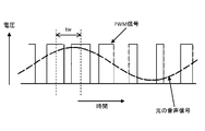
CPU11は、ドライバー12Bに基づいてマイコン10C内蔵のタイマ13を制御することにより、PCM形式のアナログ波形の音声信号に応じたPWM信号を生成する。図3に示すように、PWM信号は、出力パルスの周期twは一定である。一方、PWM信号は、入力されるアナログ波形の音声信号の大きさに応じて、パルスの「H」(ハイレベル)と「L」(ロウレベル)の時間(幅)が異なる。
The CPU 11 controls the timer 13 built in the microcomputer 10C based on the driver 12B, thereby generating a PWM signal corresponding to the PCM format analog waveform audio signal. As shown in FIG. 3, the PWM signal has a constant output pulse period tw. On the other hand, in the PWM signal, the time (width) of the pulse “H” (high level) and “L” (low level) differs depending on the magnitude of the input analog waveform audio signal.
すなわち、タイマ13は、ドライバー12Bの制御に従って、PCM形式の音声信号の信号レベルの大きさに応じたパルス幅のPWM信号に変換する。PCM形式の音声信号の信号レベルが「0」のときは、パルスの「H」と「L」の幅が同じであるPWM信号が生成される。また、PCM形式の音声信号の信号レベルが「プラス」の区間は、パルスの「H」の幅が「L」の幅よりも大きく、信号レベルが大きいほど「H」の幅が大きくなるようにPWM信号が生成される。また、PCM形式の音声信号の信号レベルが「マイナス」の区間は、パルスの「L」の幅が「H」の幅よりも大きく、信号レベルが大きいほど「L」の幅が大きくなるようにPWM信号が生成される。
That is, the timer 13 converts it into a PWM signal having a pulse width corresponding to the magnitude of the signal level of the PCM format audio signal according to the control of the driver 12B. When the signal level of the PCM audio signal is “0”, a PWM signal having the same width of “H” and “L” of the pulse is generated. Further, in the section where the signal level of the PCM format audio signal is “plus”, the width of “H” of the pulse is larger than the width of “L”, and the width of “H” becomes larger as the signal level is larger. A PWM signal is generated. Further, in a section where the signal level of the PCM format audio signal is “minus”, the width of “L” of the pulse is larger than the width of “H”, and the width of “L” becomes larger as the signal level is larger. A PWM signal is generated.
上記したように、タイマ13は、PCM形式の音声信号の大きさに比例したパルス幅のPWM信号(デジタルパルス)を生成する。そして、図2に示すように、マイコン10Cは、タイマ13が生成した2つのPWM信号を2つの出力ピンからHブリッジ回路20Cに出力する。
As described above, the timer 13 generates a PWM signal (digital pulse) having a pulse width proportional to the size of the PCM audio signal. As shown in FIG. 2, the microcomputer 10C outputs the two PWM signals generated by the timer 13 from the two output pins to the H bridge circuit 20C.
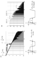
図4は、PWM信号の周波数成分を示す図である。図4(A)はデューティ比50%の場合のPWM信号の周波数成分を示し、図4(B)はデューティ比50%以外の場合のPWM信号の周波数成分を示す。ここで、デューティ比とは、1周期の中で信号レベルが「H」である割合をいう。
FIG. 4 is a diagram showing frequency components of the PWM signal. 4A shows the frequency component of the PWM signal when the duty ratio is 50%, and FIG. 4B shows the frequency component of the PWM signal when the duty ratio is other than 50%. Here, the duty ratio refers to a ratio at which the signal level is “H” in one cycle.
デジタル回路の発生するノイズの源の一つに高調波がある。PWM信号に含まれる高調波について説明する。一般に、一定の繰り返し周期をもつ全ての波は、繰り返し周波数である基本波と、その整数倍の周波数を持つ高調波に分解することができる。基本波に対する倍数を、高調波の次数と呼ぶ。PWM信号は繰り返す波形が多いので、周波数分布(スペクトラムという。)を観測すると高調波に分解され、離散的なスペクトラムに見える。
One of the sources of noise generated by digital circuits is harmonics. The harmonics included in the PWM signal will be described. In general, all waves having a fixed repetition period can be decomposed into a fundamental wave having a repetition frequency and a harmonic having a frequency that is an integral multiple of the fundamental wave. The multiple of the fundamental wave is called the harmonic order. Since the PWM signal has many repeated waveforms, when the frequency distribution (referred to as spectrum) is observed, it is decomposed into harmonics and looks like a discrete spectrum.
図4(A)に示すデューティ比50%の場合、PWM信号に含まれる高調波は、f1(=1/πT)からf2(=1/πtr)までの周波数では-20dB/decで減衰し、f2以上の周波数では-40dB/decで減衰する。ここで、Tはパルスの周期を表し、trはパルスの立ち上がり時間を表している。図4(B)に示すデューティ比50%以外の場合、PWM信号に含まれる高調波は、1/πτ以下の周波数では減衰せず、1/πτから1/πτrまでの周波数では-20dB/decで減衰し、1/πτr以上の周波数では-40dB/decで減衰する。ここで、τはパルス幅を表し、τrはパルスの立ち上がり時間を表している。
When the duty ratio is 50% shown in FIG. 4A, the harmonics included in the PWM signal are attenuated by −20 dB / dec at frequencies from f1 (= 1 / πT) to f2 (= 1 / πtr), At frequencies above f2, it attenuates at −40 dB / dec. Here, T represents the pulse period, and tr represents the pulse rise time. When the duty ratio is not 50% shown in FIG. 4B, the harmonics included in the PWM signal are not attenuated at a frequency of 1 / πτ or less, and −20 dB / dec at frequencies from 1 / πτ to 1 / πτr. And attenuates at −40 dB / dec at frequencies greater than 1 / πτr. Here, τ represents the pulse width, and τr represents the rise time of the pulse.
PWM信号の高調波のうち、周波数の高い(次数の大きい)成分は、容易に放射され、ノイズの原因になりやすい性質がある。そこで、信号波形への影響が少ない高次の高調波を除去することが、ノイズ対策として行われる。
Of the harmonics of the PWM signal, high frequency (high order) components are easily radiated and tend to cause noise. Therefore, removal of high-order harmonics having little influence on the signal waveform is performed as a noise countermeasure.
図5は、図1に示すHブリッジ回路20Cの構成を示す回路図である。図5に示すように、Hブリッジ回路20Cは、4つのバイポーラトランジスタTr1~Tr4を備えている。以下、バイポーラトランジスタTr1~Tr4を単にトランジスタTr1~Tr4と記す。
FIG. 5 is a circuit diagram showing the configuration of the H-bridge circuit 20C shown in FIG. As shown in FIG. 5, the H-bridge circuit 20C includes four bipolar transistors Tr1 to Tr4. Hereinafter, the bipolar transistors Tr1 to Tr4 are simply referred to as transistors Tr1 to Tr4.
トランジスタTr1,Tr3はPNPトランジスタであり、トランジスタTr2,Tr4はNPNトランジスタである。PNPトランジスタ(トランジスタTr1,Tr3)は、電源電圧Vccに対して低い電圧がベースに印加されたときにオンとなる。NPNトランジスタ(トランジスタTr2,Tr4)は、グラウンドに対して高い電圧がベースに印加されたときにオンとなる。
Transistors Tr1 and Tr3 are PNP transistors, and transistors Tr2 and Tr4 are NPN transistors. The PNP transistors (transistors Tr1 and Tr3) are turned on when a voltage lower than the power supply voltage Vcc is applied to the base. The NPN transistors (transistors Tr2 and Tr4) are turned on when a high voltage with respect to the ground is applied to the base.
トランジスタTr1のエミッタ端子は電圧Vcc(例えば電圧値15V)の電源と接続されている。トランジスタTr1のコレクタ端子はトランジスタTr2のコレクタ端子と接続されている。トランジスタTr1のベース端子と電源との間に抵抗R1(例えば抵抗値33kΩ)が接続されている。また、トランジスタTr1のベース端子と電源との間にショットキーバリアダイオードSBD1が抵抗R1と並列に接続されている。トランジスタTr1のベース端子とトランジスタTr2のベース端子との間にコンデンサC1(例えば容量0.1μF)が接続されている。トランジスタTr2のベース端子はPWM信号(PWMφ)を入力する信号入力端子と接続され、トランジスタTr2のエミッタ端子はグラウンドと接続されている。
The emitter terminal of the transistor Tr1 is connected to a power source having a voltage Vcc (for example, a voltage value of 15 V). The collector terminal of the transistor Tr1 is connected to the collector terminal of the transistor Tr2. A resistor R1 (for example, a resistance value of 33 kΩ) is connected between the base terminal of the transistor Tr1 and the power supply. A Schottky barrier diode SBD1 is connected in parallel with the resistor R1 between the base terminal of the transistor Tr1 and the power supply. A capacitor C1 (for example, a capacitance of 0.1 μF) is connected between the base terminal of the transistor Tr1 and the base terminal of the transistor Tr2. The base terminal of the transistor Tr2 is connected to a signal input terminal for inputting a PWM signal (PWMφ), and the emitter terminal of the transistor Tr2 is connected to the ground.
トランジスタTr3,Tr4、抵抗R2、ショットキーバリアダイオードSBD2、及びコンデンサC2からなる回路の構成は、トランジスタTr1,Tr2、抵抗R1、ショットキーバリアダイオードSBD1、及びコンデンサC1からなる回路の構成と同様である。すなわち、トランジスタTr3のエミッタ端子は電圧Vccの電源と接続されている。トランジスタTr3のコレクタ端子はトランジスタTr4のコレクタ端子と接続されている。トランジスタTr3のベース端子と電源との間に抵抗R2(例えば抵抗値33kΩ)が接続されている。また、トランジスタTr3のベース端子と電源との間にショットキーバリアダイオードSBD2が抵抗R2と並列に接続されている。トランジスタTr3のベース端子とトランジスタTr4のベース端子との間にコンデンサC2(例えば容量0.1μF)が接続されている。トランジスタTr4のベース端子はPWM信号(PWMφ)を入力する信号入力端子と接続され、トランジスタTr4のエミッタ端子はグラウンドと接続されている。
The configuration of the circuit including the transistors Tr3 and Tr4, the resistor R2, the Schottky barrier diode SBD2, and the capacitor C2 is the same as the configuration of the circuit including the transistors Tr1 and Tr2, the resistor R1, the Schottky barrier diode SBD1, and the capacitor C1. . That is, the emitter terminal of the transistor Tr3 is connected to the power supply of the voltage Vcc. The collector terminal of the transistor Tr3 is connected to the collector terminal of the transistor Tr4. A resistor R2 (for example, a resistance value of 33 kΩ) is connected between the base terminal of the transistor Tr3 and the power supply. A Schottky barrier diode SBD2 is connected in parallel with the resistor R2 between the base terminal of the transistor Tr3 and the power supply. A capacitor C2 (for example, a capacitance of 0.1 μF) is connected between the base terminal of the transistor Tr3 and the base terminal of the transistor Tr4. The base terminal of the transistor Tr4 is connected to a signal input terminal for inputting a PWM signal (PWMφ), and the emitter terminal of the transistor Tr4 is connected to the ground.
トランジスタTr1のコレクタ端子とトランジスタTr2のコレクタ端子との接続点と、トランジスタTr3のコレクタ端子とトランジスタTr4のコレクタ端子との接続点との間に、圧電素子PZ及び抵抗R0が直列に接続されている。圧電素子PZの電気的特性はコンデンサ(キャパシタ)である(つまり、圧電素子PZはコンデンサと等価である)。従って、圧電素子PZと抵抗R0とで1次ローパスフィルタを構成する。なお、圧電素子PZにおけるコンデンサとしての容量は例えば50nFであり、抵抗R0の抵抗値は例えば1kΩであるものとする。本実施形態では、圧電素子PZと抵抗R0とで圧電ブザー60を構成する。
A piezoelectric element PZ and a resistor R0 are connected in series between a connection point between the collector terminal of the transistor Tr1 and the collector terminal of the transistor Tr2 and a connection point between the collector terminal of the transistor Tr3 and the collector terminal of the transistor Tr4. . The electrical characteristic of the piezoelectric element PZ is a capacitor (capacitor) (that is, the piezoelectric element PZ is equivalent to a capacitor). Therefore, the piezoelectric element PZ and the resistor R0 constitute a primary low-pass filter. The capacitance as a capacitor in the piezoelectric element PZ is, for example, 50 nF, and the resistance value of the resistor R0 is, for example, 1 kΩ. In the present embodiment, the piezoelectric buzzer 60 is composed of the piezoelectric element PZ and the resistor R0.
なお、Hブリッジ回路20Cを構成する各素子の値(抵抗値、容量値)や圧電ブザー60を構成する各素子(圧電素子PZ、抵抗R0)の値(抵抗値、容量値)は一例であって、上記の値に限定されるわけではなく、圧電素子PZの特性などに合わせて適宜設定される。
Note that the values (resistance value, capacitance value) of each element constituting the H-bridge circuit 20C and the values (resistance value, capacitance value) of each element (piezoelectric element PZ, resistance R0) constituting the piezoelectric buzzer 60 are examples. Thus, the value is not limited to the above value, and is appropriately set according to the characteristics of the piezoelectric element PZ.
Hブリッジ回路20Cにおいて、4つのトランジスタTr1~Tr4がオフの場合、圧電素子PZ及び抵抗R0には電圧が印加されない。トランジスタTr1及びトランジスタTr4がオンであり、トランジスタTr2及びトランジスタTr3がオフのとき、図5の(1)の経路(電源電圧Vcc、トランジスタTr1、抵抗R0、圧電素子PZ、トランジスタTr4、グラウンド)で電流が流れる。一方、トランジスタTr2及びトランジスタTr3がオンであり、トランジスタTr1及びトランジスタTr4がオフのとき、図5の(2)の経路(電源電圧Vcc、トランジスタTr3、圧電素子PZ、抵抗R0、トランジスタTr2、グラウンド)で電流が流れる。
In the H-bridge circuit 20C, when the four transistors Tr1 to Tr4 are off, no voltage is applied to the piezoelectric element PZ and the resistor R0. When the transistor Tr1 and the transistor Tr4 are on and the transistor Tr2 and the transistor Tr3 are off, a current flows through the path (1) in FIG. 5 (power supply voltage Vcc, transistor Tr1, resistor R0, piezoelectric element PZ, transistor Tr4, ground). Flows. On the other hand, when the transistors Tr2 and Tr3 are on and the transistors Tr1 and Tr4 are off, the path (2) in FIG. 5 (power supply voltage Vcc, transistor Tr3, piezoelectric element PZ, resistor R0, transistor Tr2, ground) Current flows.
トランジスタTr1,Tr2のベース端子は、それぞれ、抵抗R1によって電圧Vccよりも低い電圧が印加されている。すなわち、トランジスタTr1のベース端子の電位は、トランジスタTr1のエミッタ端子の電位よりも低くなっている。また、トランジスタTr2のベース端子の電位は、トランジスタTr2のコレクタ端子の電位(0V)よりも高くなっている。
A voltage lower than the voltage Vcc is applied to the base terminals of the transistors Tr1 and Tr2 by the resistor R1. That is, the potential of the base terminal of the transistor Tr1 is lower than the potential of the emitter terminal of the transistor Tr1. In addition, the potential of the base terminal of the transistor Tr2 is higher than the potential (0 V) of the collector terminal of the transistor Tr2.
このような状態において、信号入力端子から入力されるPWM信号が「H」のときは、トランジスタTr1がオフとなり、トランジスタTr2がオンとなる。また、信号入力端子から入力されるPWM信号が「L」のときは、トランジスタTr1がオンとなり、トランジスタTr2がオフとなる。同様に、信号入力端子から入力されるPWM信号が「H」のときは、トランジスタTr3がオフとなり、トランジスタTr4がオンとなる。また、信号入力端子から入力されるPWM信号が「L」のときは、トランジスタTr3がオンとなり、トランジスタTr4がオフとなる。このように、Hブリッジ回路20Cは、4つのトランジスタ(スイッチ)のうち対角線上にある二組のトランジスタが交互にオンすることで負荷の電流方向を逆向きにすることができ、電池の持つ電圧を最大限に活かすことができる。
In such a state, when the PWM signal input from the signal input terminal is “H”, the transistor Tr1 is turned off and the transistor Tr2 is turned on. When the PWM signal input from the signal input terminal is “L”, the transistor Tr1 is turned on and the transistor Tr2 is turned off. Similarly, when the PWM signal input from the signal input terminal is “H”, the transistor Tr3 is turned off and the transistor Tr4 is turned on. When the PWM signal input from the signal input terminal is “L”, the transistor Tr3 is turned on and the transistor Tr4 is turned off. Thus, the H bridge circuit 20C can reverse the current direction of the load by alternately turning on the two transistors on the diagonal line among the four transistors (switches), and the voltage of the battery Can make the most of it.
上記したように、Hブリッジ回路20Cの電源電圧を15Vとしているのに対して、小さなボタン型電池(コイン型電池ともいう。)の電圧は1V~3V程度である。ボタン型電池を用いてHブリッジ回路20Cを駆動する場合、チャージポンプでボタン型電池の電圧を電源電圧まで昇圧させる。これにより、本発明の音声再生装置をヘルスケア製品(例えば体温計、血糖値計)などの小さな機器にも搭載することが可能となる。
As described above, while the power supply voltage of the H-bridge circuit 20C is 15V, the voltage of a small button-type battery (also called a coin-type battery) is about 1V to 3V. When the H-bridge circuit 20C is driven using a button type battery, the voltage of the button type battery is boosted to the power supply voltage by the charge pump. As a result, the sound reproducing device of the present invention can be mounted on a small device such as a health care product (for example, a thermometer or a blood glucose meter).
図6は、本発明の圧電ブザー60の構成を示す図である。図6に示す圧電素子(圧電振動板)は、薄い円板状の圧電体(圧電セラミックス)61と、黄銅やニッケルなどの薄い円板状の金属板62とを貼り合わせた(接着した)構造である。このような圧電素子の構造をユニモルフ構造という。圧電体61の表面には電極が形成され、その電極にリード(ケーブル)63が接続されている。また、金属板62の表面にも電極が形成され、その電極にリード(ケーブル)64が接続されている。抵抗65がリード64の途中に接続されている。圧電体61及び金属板62が図5に示した圧電素子PZに相当し、抵抗65が図5に示した抵抗R0に相当する。なお、抵抗65はリード64の途中ではなくリード63の途中に接続されてもよい。
FIG. 6 is a diagram showing the configuration of the piezoelectric buzzer 60 of the present invention. The piezoelectric element (piezoelectric vibration plate) shown in FIG. 6 has a structure in which a thin disk-shaped piezoelectric body (piezoelectric ceramics) 61 and a thin disk-shaped metal plate 62 such as brass or nickel are bonded (bonded). It is. Such a piezoelectric element structure is called a unimorph structure. Electrodes are formed on the surface of the piezoelectric body 61, and leads (cables) 63 are connected to the electrodes. An electrode is also formed on the surface of the metal plate 62, and a lead (cable) 64 is connected to the electrode. A resistor 65 is connected in the middle of the lead 64. The piezoelectric body 61 and the metal plate 62 correspond to the piezoelectric element PZ shown in FIG. 5, and the resistor 65 corresponds to the resistor R0 shown in FIG. The resistor 65 may be connected not in the middle of the lead 64 but in the middle of the lead 63.
圧電素子に電圧が印加されると圧電体61が伸びるが、圧電体61に接着している金属板62は伸縮せずに所定方向に曲がる。また、圧電素子に逆方向の電圧が印加されると圧電体61が縮むが、圧電体61に接着している金属板62は伸縮せずに所定方向とは逆方向に曲がる。圧電素子に電圧の向きが交互に変わる信号電圧が印加されると両方向の振動が発生して音波が発生する。
When a voltage is applied to the piezoelectric element, the piezoelectric body 61 expands, but the metal plate 62 bonded to the piezoelectric body 61 bends in a predetermined direction without expanding and contracting. Further, when a voltage in the reverse direction is applied to the piezoelectric element, the piezoelectric body 61 contracts, but the metal plate 62 bonded to the piezoelectric body 61 does not expand and contract and bends in a direction opposite to the predetermined direction. When a signal voltage whose voltage direction changes alternately is applied to the piezoelectric element, vibrations in both directions are generated and sound waves are generated.
本実施形態では、圧電体(圧電セラミックス)と金属板とで構成される素子を圧電素子といい、圧電素子と抵抗とを含む構成を圧電ブザーという。なお、一般には、圧電体(圧電セラミックス)のことを圧電素子という場合があり、また、圧電体と金属板とで構成される素子を圧電ブザーという場合もある。また、圧電ブザーは、圧電スピーカー(ピエゾスピーカー)、圧電サウンダーなどと呼ばれ、明確に区別されていないが、本実施形態における圧電ブザーは、上記の圧電スピーカー(ピエゾスピーカー)、圧電サウンダーなどを含む構成である。
In this embodiment, an element composed of a piezoelectric body (piezoelectric ceramics) and a metal plate is referred to as a piezoelectric element, and a structure including a piezoelectric element and a resistor is referred to as a piezoelectric buzzer. In general, a piezoelectric body (piezoelectric ceramic) may be referred to as a piezoelectric element, and an element constituted by a piezoelectric body and a metal plate may be referred to as a piezoelectric buzzer. In addition, the piezoelectric buzzer is called a piezoelectric speaker (piezo speaker), a piezoelectric sounder, and the like, and is not clearly distinguished. However, the piezoelectric buzzer in the present embodiment includes the piezoelectric speaker (piezo speaker), the piezoelectric sounder, and the like. It is a configuration.
圧電素子としては、圧電体の材料、径、厚さや、金属板の材料、径、厚さなどに応じて特性が変化する。例えば、圧電素子によって、共振点(共振周波数)、共振抵抗、静電容量が変化する。上述したように、本発明は、安価な圧電ブザーを用いて高音質の音声出力を実現することを目的としているため、本実施形態では、電子ブザーとして利用されるような圧電素子を用いることを想定している。
The characteristics of the piezoelectric element vary depending on the material, diameter, and thickness of the piezoelectric body and the material, diameter, and thickness of the metal plate. For example, the resonance point (resonance frequency), the resonance resistance, and the capacitance are changed by the piezoelectric element. As described above, the present invention is intended to achieve high-quality sound output using an inexpensive piezoelectric buzzer. Therefore, in this embodiment, a piezoelectric element used as an electronic buzzer is used. Assumed.
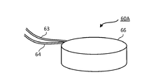
図7は、圧電素子及び抵抗がパッケージ66に収納された圧電ブザー60Aの構成を示す斜視図である。図7に示すように、圧電体61と金属板62とで構成される圧電素子と、その圧電素子に接続された抵抗65とがパッケージ66内に収容されている。このような構成の場合、圧電素子と抵抗65とが1つの部品として構成されることとなる。
FIG. 7 is a perspective view showing a configuration of a piezoelectric buzzer 60A in which a piezoelectric element and a resistor are housed in a package 66. FIG. As shown in FIG. 7, a piezoelectric element composed of a piezoelectric body 61 and a metal plate 62 and a resistor 65 connected to the piezoelectric element are housed in a package 66. In such a configuration, the piezoelectric element and the resistor 65 are configured as one component.
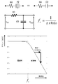
図8は、1次ローパスフィルタの回路図及び1次ローパスフィルタの周波数特性を示すグラフである。上述したように、圧電素子PZは電気的特性としてコンデンサ(キャパシタ)C0とみなされる。図8の回路図に示すように、抵抗R0とコンデンサC0とで構成されるRC回路は1次ローパスフィルタ(RCフィルタ)として機能する。RC回路の折れ点周波数fcは、fc=1/(2π・R0・C0)となる。図8のグラフに示すように、RC回路からなる1次ローパスフィルタは、RC回路の折れ点周波数fc以下の周波数の信号を通過させ、RC回路の折れ点周波数fc以上の周波数の信号を-20dB/decで減衰させる。
FIG. 8 is a circuit diagram of the primary low-pass filter and a graph showing the frequency characteristics of the primary low-pass filter. As described above, the piezoelectric element PZ is regarded as the capacitor C0 as an electrical characteristic. As shown in the circuit diagram of FIG. 8, the RC circuit including the resistor R0 and the capacitor C0 functions as a primary low-pass filter (RC filter). The break frequency fc of the RC circuit is fc = 1 / (2π · R0 · C0). As shown in the graph of FIG. 8, the first-order low-pass filter formed of the RC circuit passes a signal having a frequency equal to or lower than the break frequency fc of the RC circuit, and a signal having a frequency equal to or higher than the break frequency fc of the RC circuit is −20 dB. Attenuate at / dec.
本実施形態では、圧電素子PZと抵抗R0とで構成するRC回路の折れ点周波数fcが圧電素子PZの共振点(共振周波数)以下としている。このような構成によれば、圧電素子PZの共振点よりも高い周波数成分をRCフィルタで抑制することができ、人の声や音楽などを高音質で出力することが可能となる。
In the present embodiment, the break frequency fc of the RC circuit constituted by the piezoelectric element PZ and the resistor R0 is set to be equal to or lower than the resonance point (resonance frequency) of the piezoelectric element PZ. According to such a configuration, a frequency component higher than the resonance point of the piezoelectric element PZ can be suppressed by the RC filter, and it becomes possible to output a human voice or music with high sound quality.
また、圧電素子PZと抵抗R0とで構成するRC回路の折れ点周波数の1/2が圧電素子PZの共振点以下としてもよい。このような構成によれば、より高い周波数成分をRCフィルタで抑制することができ、より一層、人の声や音楽などを高音質で出力することが可能となる。
Further, 1/2 of the break frequency of the RC circuit constituted by the piezoelectric element PZ and the resistor R0 may be equal to or lower than the resonance point of the piezoelectric element PZ. According to such a configuration, higher frequency components can be suppressed by the RC filter, and it becomes possible to further output a human voice or music with high sound quality.
圧電素子PZと直列に接続される抵抗R0(図6の抵抗65)には、以下に示す4つの役割がある。
1.上述したように、圧電素子と等価であるコンデンサとともにRCフィルタ(1次ローパスフィルタ)を形成する役割がある。
2.圧電ブザー60に存在する機械振動の共振のQを下げる役割がある。一般に、圧電ブザーは電子ブザーとして使用されるので、故意にQの高い機械振動が起きやすいように設計されている。本実施形態では、圧電素子PZの特性に合わせて抵抗R0の抵抗値を調整することで1次ローパスフィルタの通過帯域を設定することができる。この通過帯域を適切に設定することで可聴帯域外の信号の抑圧し、また可聴帯域内の圧電ブザーの機械振動のQを下げることが可能となる。
3.PWM信号に存在する、矩形波の高次高調波における圧電素子のインピーダンスを下げる役割がある。このような役割によって圧電ブザー60を電池で駆動することが可能となる。
4.圧電素子では高音を出力しやすいように設計されているが、その高音の出力を抑えて特性をフラットにする役割がある。 The resistor R0 (resistor 65 in FIG. 6) connected in series with the piezoelectric element PZ has the following four roles.
1. As described above, there is a role of forming an RC filter (primary low-pass filter) together with a capacitor equivalent to a piezoelectric element.
2. It plays a role of lowering the Q of mechanical vibration resonance existing in thepiezoelectric buzzer 60. In general, since a piezoelectric buzzer is used as an electronic buzzer, it is intentionally designed so that mechanical vibration with a high Q is likely to occur. In the present embodiment, the pass band of the primary low-pass filter can be set by adjusting the resistance value of the resistor R0 in accordance with the characteristics of the piezoelectric element PZ. By appropriately setting the pass band, signals outside the audible band can be suppressed, and the mechanical vibration Q of the piezoelectric buzzer within the audible band can be reduced.
3. There is a role of lowering the impedance of the piezoelectric element in the high-order harmonics of the rectangular wave existing in the PWM signal. With such a role, thepiezoelectric buzzer 60 can be driven by a battery.
4). Piezoelectric elements are designed to output high sounds easily, but have the role of flattening the characteristics by suppressing the output of high sounds.
1.上述したように、圧電素子と等価であるコンデンサとともにRCフィルタ(1次ローパスフィルタ)を形成する役割がある。
2.圧電ブザー60に存在する機械振動の共振のQを下げる役割がある。一般に、圧電ブザーは電子ブザーとして使用されるので、故意にQの高い機械振動が起きやすいように設計されている。本実施形態では、圧電素子PZの特性に合わせて抵抗R0の抵抗値を調整することで1次ローパスフィルタの通過帯域を設定することができる。この通過帯域を適切に設定することで可聴帯域外の信号の抑圧し、また可聴帯域内の圧電ブザーの機械振動のQを下げることが可能となる。
3.PWM信号に存在する、矩形波の高次高調波における圧電素子のインピーダンスを下げる役割がある。このような役割によって圧電ブザー60を電池で駆動することが可能となる。
4.圧電素子では高音を出力しやすいように設計されているが、その高音の出力を抑えて特性をフラットにする役割がある。 The resistor R0 (
1. As described above, there is a role of forming an RC filter (primary low-pass filter) together with a capacitor equivalent to a piezoelectric element.
2. It plays a role of lowering the Q of mechanical vibration resonance existing in the
3. There is a role of lowering the impedance of the piezoelectric element in the high-order harmonics of the rectangular wave existing in the PWM signal. With such a role, the
4). Piezoelectric elements are designed to output high sounds easily, but have the role of flattening the characteristics by suppressing the output of high sounds.
以上に説明したように、本実施形態では、抵抗R0が圧電素子PZに直列に接続され、圧電素子PZと等価であるキャパシタC0と抵抗R0とでローパスフィルタを形成するので、安価な圧電ブザーを使用することができ、コストを大幅に削減することができる。また、そのような安価な圧電ブザー60を使用した場合であっても、高音質の音声出力を実現することができる。また、ローパスフィルタで高い周波数成分を抑制するので、低消費電流で圧電ブザー60の駆動することができる。
As described above, in this embodiment, the resistor R0 is connected in series to the piezoelectric element PZ, and the capacitor C0 equivalent to the piezoelectric element PZ and the resistor R0 form a low-pass filter. Can be used and the cost can be greatly reduced. Even when such an inexpensive piezoelectric buzzer 60 is used, high-quality sound output can be realized. Moreover, since the high frequency component is suppressed by the low-pass filter, the piezoelectric buzzer 60 can be driven with low current consumption.
本発明の圧電ブザー及び音声再生装置は、ガイド音声を出力する機器として用いることができる。例えば、鉄道やバス等の車内/構内アナウンス、信号、ビル入退管理端末、監視カメラ、医療機器、AED(Automated External Defibrillator;自動体外式除細動器)、産業用プリンタ、オフィス用複合プリンタ、民生用インクジェットプリンタ、アミューズメント機器の効果音などに利用可能である。また、本発明の圧電ブザー及び音声再生装置は、厳しい温度/環境条件下での音声出力する機器として用いることができる。例えば、火災/ガス/避難警報、建設機械、自動車、自販機、ATMなどに利用可能である。
The piezoelectric buzzer and sound reproducing device of the present invention can be used as a device that outputs a guide sound. For example, in-car / premises announcements such as railways and buses, signals, building entry / exit management terminals, surveillance cameras, medical equipment, AED (Automated External Defibrillator), industrial printers, composite printers for offices, It can be used for sound effects of consumer inkjet printers and amusement machines. Further, the piezoelectric buzzer and the sound reproducing device of the present invention can be used as a device for outputting sound under severe temperature / environment conditions. For example, it can be used for fire / gas / evacuation alarms, construction machines, automobiles, vending machines, ATMs, and the like.
以上、本発明の実施形態を説明したが、本発明の技術的範囲は、上記の実施形態に記載の範囲には限定されない。本発明の趣旨を逸脱しない範囲で、上記の実施形態に、多様な変更または改良を加えることが可能である。また、上記の実施形態で説明した要件の1つ以上は、省略されることがある。そのような変更または改良、省略した形態も本発明の技術的範囲に含まれる。また、上記した実施形態や変形例の構成を適宜組み合わせて適用することも可能である。
As mentioned above, although embodiment of this invention was described, the technical scope of this invention is not limited to the range as described in said embodiment. Various modifications or improvements can be added to the above-described embodiment without departing from the spirit of the present invention. In addition, one or more of the requirements described in the above embodiments may be omitted. Such modifications, improvements, and omitted forms are also included in the technical scope of the present invention. In addition, the configurations of the above-described embodiments and modifications can be applied in appropriate combinations.
例えば、上記の実施形態では、圧電素子PZの2つの端子の一方に抵抗を接続していたが、2つの端子の両方に抵抗を接続してもよい。このような場合でもRCフィルタとして機能させることができる。また、圧電素子は、ユニモルフ構造の素子を用いていたが、バイモルフ構造の素子や積層タイプの素子を用いてもよい。また、Hブリッジ回路は4つのバイポーラトランジスタで構成されたものを用いていたが、4つのFETで構成されたもの(図1(B)のHブリッジ回路20B)を用いてもよい。
For example, in the above embodiment, a resistor is connected to one of the two terminals of the piezoelectric element PZ, but a resistor may be connected to both of the two terminals. Even in such a case, it can function as an RC filter. Moreover, although the element of the unimorph structure was used for the piezoelectric element, you may use the element of a bimorph structure and a laminated | stacked type element. In addition, although the H bridge circuit is composed of four bipolar transistors, it may be composed of four FETs (H bridge circuit 20B in FIG. 1B).
10C マイクロコンピュータ
12B ドライバー
20C Hブリッジ回路(駆動回路)
60 圧電ブザー
61 圧電体
62 金属板
65 抵抗
66 パッケージ
Tr1~Tr4 バイポーラトランジスタ(トランジスタ)
R0 抵抗
PZ 圧電素子
10C microcomputer 12B driver 20C H bridge circuit (drive circuit)
60Piezoelectric buzzer 61 Piezoelectric body 62 Metal plate 65 Resistor 66 Package Tr1 to Tr4 Bipolar transistors (transistors)
R0 resistance PZ piezoelectric element
12B ドライバー
20C Hブリッジ回路(駆動回路)
60 圧電ブザー
61 圧電体
62 金属板
65 抵抗
66 パッケージ
Tr1~Tr4 バイポーラトランジスタ(トランジスタ)
R0 抵抗
PZ 圧電素子
60
R0 resistance PZ piezoelectric element
Claims (4)
- 圧電体に信号電圧を加えることで発生する前記圧電体の振動を音声として出力する、共振を利用して特定周波数の音声出力に適した圧電素子と、前記圧電素子に直列に接続され、前記圧電素子と等価であるキャパシタとともにローパスフィルタを構成する抵抗とを有し、別途のローパスフィルタを用いずに周波数成分を抑圧する圧電ブザーと、
ミドルウェアに基づいて、音声信号に応じたPWM信号を生成するマイクロコンピュータと、
前記マイクロコンピュータで生成される前記PWM信号に基づいて、Hブリッジ回路を構成する4つのバイポーラトランジスタがスイッチング動作することで電力増幅を行い、前記PWM信号に応じた低消費電流の信号電圧を前記圧電素子と該圧電素子の特性に合わせた抵抗値の前記抵抗とが直列に接続された前記圧電ブザーに出力して前記圧電ブザーの音声出力を実行する駆動回路と、を備えることを特徴とする音声再生装置。 A piezoelectric element that outputs vibrations of the piezoelectric body generated by applying a signal voltage to the piezoelectric body as sound, is suitable for sound output at a specific frequency using resonance, and is connected in series to the piezoelectric element, and the piezoelectric element A piezoelectric buzzer that has a resistor that constitutes a low-pass filter together with a capacitor equivalent to the element, and suppresses frequency components without using a separate low-pass filter;
A microcomputer that generates a PWM signal corresponding to the audio signal based on the middleware;
Based on the PWM signal generated by the microcomputer, power amplification is performed by switching operation of four bipolar transistors constituting the H-bridge circuit, and a signal voltage with low current consumption corresponding to the PWM signal is applied to the piezoelectric signal. And a drive circuit that outputs the piezoelectric buzzer by outputting the piezoelectric buzzer to the piezoelectric buzzer in which an element and the resistor having a resistance value matched to the characteristics of the piezoelectric element are connected in series. Playback device. - 前記Hブリッジ回路を構成する2つの対称の回路は、それぞれ、2つのバイポーラトランジスタのベース端子の間にコンデンサが接続され、前記コンデンサの一方の端子と電源との間にショットキーバリアダイオードが接続され、前記コンデンサの他方の端子に前記PWM信号を入力する信号入力端子が接続される請求項1記載の音声再生装置。 In each of the two symmetrical circuits constituting the H-bridge circuit, a capacitor is connected between base terminals of two bipolar transistors, and a Schottky barrier diode is connected between one terminal of the capacitor and a power supply. The audio reproduction device according to claim 1, wherein a signal input terminal for inputting the PWM signal is connected to the other terminal of the capacitor.
- 前記駆動回路は、電池の電圧で動作し、
前記電池の電圧を電源電圧まで昇圧させるチャージポンプを備える請求項1または請求項2記載の音声再生装置。 The drive circuit operates on battery voltage,
The sound reproducing device according to claim 1, further comprising a charge pump that boosts the voltage of the battery to a power supply voltage. - 前記マイクロコンピュータは、前記ミドルウェアとしての再生制御ミドルウェアに基づいて、圧縮された音声データをデコードしながらPCM形式の音声信号に変換し、前記ミドルウェアとしてのドライバーに基づいて、前記音声信号に応じたPWM信号を生成して前記駆動回路に出力する請求項1から請求項3のいずれか1項記載の音声再生装置。
The microcomputer converts the compressed audio data into a PCM format audio signal while decoding the compressed audio data based on the playback control middleware as the middleware, and the PWM corresponding to the audio signal based on the driver as the middleware The sound reproducing device according to any one of claims 1 to 3, wherein a signal is generated and output to the driving circuit.
Applications Claiming Priority (2)
| Application Number | Priority Date | Filing Date | Title |
|---|---|---|---|
| JP2016-255204 | 2016-12-28 | ||
| JP2016255204A JP6308696B1 (en) | 2016-12-28 | 2016-12-28 | Audio playback device |
Publications (1)
| Publication Number | Publication Date |
|---|---|
| WO2018123730A1 true WO2018123730A1 (en) | 2018-07-05 |
Family
ID=61901947
Family Applications (1)
| Application Number | Title | Priority Date | Filing Date |
|---|---|---|---|
| PCT/JP2017/045521 WO2018123730A1 (en) | 2016-12-28 | 2017-12-19 | Audio reproduction device |
Country Status (2)
| Country | Link |
|---|---|
| JP (1) | JP6308696B1 (en) |
| WO (1) | WO2018123730A1 (en) |
Cited By (1)
| Publication number | Priority date | Publication date | Assignee | Title |
|---|---|---|---|---|
| US11647331B2 (en) | 2019-10-29 | 2023-05-09 | Seiko Epson Corporation | Circuit device, sound reproduction device, and electronic apparatus |
Families Citing this family (2)
| Publication number | Priority date | Publication date | Assignee | Title |
|---|---|---|---|---|
| CN109407579B (en) * | 2018-10-16 | 2021-06-01 | 浩云科技股份有限公司 | Independent sound wave algorithm control circuit |
| JP7427529B2 (en) | 2020-05-29 | 2024-02-05 | キヤノン株式会社 | Buzzer control device, FAX communication device, and buzzer control method |
Citations (7)
| Publication number | Priority date | Publication date | Assignee | Title |
|---|---|---|---|---|
| JPS59146296A (en) * | 1983-02-08 | 1984-08-22 | Murata Mfg Co Ltd | Driving method of piezoelectric speaker |
| JPS6021694A (en) * | 1983-07-18 | 1985-02-04 | Nippon Telegr & Teleph Corp <Ntt> | Piezoelectric receiver |
| JPH06186980A (en) * | 1992-12-15 | 1994-07-08 | New Japan Radio Co Ltd | Sounding body driving circuit |
| JPH077788A (en) * | 1993-03-19 | 1995-01-10 | Ford Motor Co | Sound reproduction system and sound reproduction method |
| JP2006094158A (en) * | 2004-09-24 | 2006-04-06 | Nec Access Technica Ltd | Drive circuit, and portable device having the same |
| JP2007033939A (en) * | 2005-07-27 | 2007-02-08 | Denso Corp | Piezo-electric buzzer driving circuit |
| WO2007132839A1 (en) * | 2006-05-15 | 2007-11-22 | Asahi Kasei Emd Corporation | Drive device, drive method, and information device |
-
2016
- 2016-12-28 JP JP2016255204A patent/JP6308696B1/en active Active
-
2017
- 2017-12-19 WO PCT/JP2017/045521 patent/WO2018123730A1/en active Application Filing
Patent Citations (7)
| Publication number | Priority date | Publication date | Assignee | Title |
|---|---|---|---|---|
| JPS59146296A (en) * | 1983-02-08 | 1984-08-22 | Murata Mfg Co Ltd | Driving method of piezoelectric speaker |
| JPS6021694A (en) * | 1983-07-18 | 1985-02-04 | Nippon Telegr & Teleph Corp <Ntt> | Piezoelectric receiver |
| JPH06186980A (en) * | 1992-12-15 | 1994-07-08 | New Japan Radio Co Ltd | Sounding body driving circuit |
| JPH077788A (en) * | 1993-03-19 | 1995-01-10 | Ford Motor Co | Sound reproduction system and sound reproduction method |
| JP2006094158A (en) * | 2004-09-24 | 2006-04-06 | Nec Access Technica Ltd | Drive circuit, and portable device having the same |
| JP2007033939A (en) * | 2005-07-27 | 2007-02-08 | Denso Corp | Piezo-electric buzzer driving circuit |
| WO2007132839A1 (en) * | 2006-05-15 | 2007-11-22 | Asahi Kasei Emd Corporation | Drive device, drive method, and information device |
Cited By (1)
| Publication number | Priority date | Publication date | Assignee | Title |
|---|---|---|---|---|
| US11647331B2 (en) | 2019-10-29 | 2023-05-09 | Seiko Epson Corporation | Circuit device, sound reproduction device, and electronic apparatus |
Also Published As
| Publication number | Publication date |
|---|---|
| JP6308696B1 (en) | 2018-04-11 |
| JP2018107752A (en) | 2018-07-05 |
Similar Documents
| Publication | Publication Date | Title |
|---|---|---|
| JP6308705B1 (en) | Audio playback device | |
| US7461281B2 (en) | Capacitive load driving circuit, electrostatic transducer, method of setting circuit constant, ultrasonic speaker, display device, and directional acoustic system | |
| WO2018123730A1 (en) | Audio reproduction device | |
| JP2012022537A (en) | Piezoelectric actuator drive unit | |
| US20030228021A1 (en) | Acoustic-signal emitting device for vehicles | |
| JPS6120637Y2 (en) | ||
| JP2016046544A (en) | Switching circuit, audio amplifier integration circuit, electronic apparatus, driving method of electroacoustic conversion element | |
| US20140056442A1 (en) | Switching mode amplifier operation | |
| EP1509337B1 (en) | Electronic control circuit and acoustic-signal emitting device for vehicles | |
| JPS62161199A (en) | Vibration sound generator | |
| US20200235710A1 (en) | Transducer driver circuitry | |
| JP4426738B2 (en) | Piezoelectric speaker system | |
| US7629842B2 (en) | Class D audio amplifier | |
| WO2019131639A1 (en) | Acoustic device, acoustic control device, and program | |
| CN210202074U (en) | Analog buzzer circuit and electronic equipment | |
| US7171011B2 (en) | Acoustic drive circuit | |
| JP2016063300A (en) | Audio amplifier, electronic apparatus, and audio signal reproduction method | |
| JP6186135B2 (en) | Class D amplifier and electronic equipment | |
| JPH0453320B2 (en) | ||
| JP6474523B1 (en) | Method of eliminating noise in audio playback device | |
| WO2002095935A1 (en) | Audio output amplifier | |
| JP2021136563A (en) | Driving system, sound reproducing device, and electronic apparatus | |
| JPS63156405A (en) | Piezoelectric signal generator | |
| GB2388994A (en) | Piezoelectric sounder and drive circuit arranged to reproduce an alarm tone and a voice message | |
| JPS61112197A (en) | Piezo-electric type alarm |
Legal Events
| Date | Code | Title | Description |
|---|---|---|---|
| 121 | Ep: the epo has been informed by wipo that ep was designated in this application |
Ref document number: 17886817 Country of ref document: EP Kind code of ref document: A1 |
|
| NENP | Non-entry into the national phase |
Ref country code: DE |
|
| 122 | Ep: pct application non-entry in european phase |
Ref document number: 17886817 Country of ref document: EP Kind code of ref document: A1 |