WO2018123432A1 - Booster antenna, communication ic unit equipped with booster antenna, and communication ic unit equipped with booster antenna having attached conductor - Google Patents
Booster antenna, communication ic unit equipped with booster antenna, and communication ic unit equipped with booster antenna having attached conductor Download PDFInfo
- Publication number
- WO2018123432A1 WO2018123432A1 PCT/JP2017/043161 JP2017043161W WO2018123432A1 WO 2018123432 A1 WO2018123432 A1 WO 2018123432A1 JP 2017043161 W JP2017043161 W JP 2017043161W WO 2018123432 A1 WO2018123432 A1 WO 2018123432A1
- Authority
- WO
- WIPO (PCT)
- Prior art keywords
- conductor
- surface side
- antenna
- unit
- booster antenna
- Prior art date
Links
- 239000004020 conductor Substances 0.000 title claims abstract description 126
- 238000004891 communication Methods 0.000 title claims abstract description 59
- 239000000758 substrate Substances 0.000 claims abstract description 40
- 238000009434 installation Methods 0.000 claims abstract description 12
- 239000000463 material Substances 0.000 claims description 36
- 239000003990 capacitor Substances 0.000 claims description 16
- 230000004907 flux Effects 0.000 claims description 13
- 230000000149 penetrating effect Effects 0.000 claims description 4
- 230000006870 function Effects 0.000 abstract description 4
- 239000010410 layer Substances 0.000 description 19
- 238000000034 method Methods 0.000 description 6
- 239000002184 metal Substances 0.000 description 5
- 230000002093 peripheral effect Effects 0.000 description 5
- 239000000919 ceramic Substances 0.000 description 4
- 238000010586 diagram Methods 0.000 description 2
- 239000003822 epoxy resin Substances 0.000 description 2
- 238000005530 etching Methods 0.000 description 2
- 239000011521 glass Substances 0.000 description 2
- 238000009413 insulation Methods 0.000 description 2
- 239000010445 mica Substances 0.000 description 2
- 229910052618 mica group Inorganic materials 0.000 description 2
- 239000000088 plastic resin Substances 0.000 description 2
- 238000007747 plating Methods 0.000 description 2
- 229920000647 polyepoxide Polymers 0.000 description 2
- 229920001721 polyimide Polymers 0.000 description 2
- 239000009719 polyimide resin Substances 0.000 description 2
- 238000007639 printing Methods 0.000 description 2
- 238000007740 vapor deposition Methods 0.000 description 2
- 229920000049 Carbon (fiber) Polymers 0.000 description 1
- 239000000853 adhesive Substances 0.000 description 1
- 230000001070 adhesive effect Effects 0.000 description 1
- 230000015572 biosynthetic process Effects 0.000 description 1
- 239000004917 carbon fiber Substances 0.000 description 1
- 230000005672 electromagnetic field Effects 0.000 description 1
- 230000004927 fusion Effects 0.000 description 1
- VNWKTOKETHGBQD-UHFFFAOYSA-N methane Chemical compound C VNWKTOKETHGBQD-UHFFFAOYSA-N 0.000 description 1
- 239000011241 protective layer Substances 0.000 description 1
- 239000011347 resin Substances 0.000 description 1
- 229920005989 resin Polymers 0.000 description 1
- 239000000126 substance Substances 0.000 description 1
- XLYOFNOQVPJJNP-UHFFFAOYSA-N water Substances O XLYOFNOQVPJJNP-UHFFFAOYSA-N 0.000 description 1
- 238000004804 winding Methods 0.000 description 1
Images


Classifications
-
- G—PHYSICS
- G06—COMPUTING; CALCULATING OR COUNTING
- G06K—GRAPHICAL DATA READING; PRESENTATION OF DATA; RECORD CARRIERS; HANDLING RECORD CARRIERS
- G06K19/00—Record carriers for use with machines and with at least a part designed to carry digital markings
- G06K19/06—Record carriers for use with machines and with at least a part designed to carry digital markings characterised by the kind of the digital marking, e.g. shape, nature, code
- G06K19/067—Record carriers with conductive marks, printed circuits or semiconductor circuit elements, e.g. credit or identity cards also with resonating or responding marks without active components
- G06K19/07—Record carriers with conductive marks, printed circuits or semiconductor circuit elements, e.g. credit or identity cards also with resonating or responding marks without active components with integrated circuit chips
- G06K19/077—Constructional details, e.g. mounting of circuits in the carrier
-
- H—ELECTRICITY
- H01—ELECTRIC ELEMENTS
- H01Q—ANTENNAS, i.e. RADIO AERIALS
- H01Q1/00—Details of, or arrangements associated with, antennas
- H01Q1/36—Structural form of radiating elements, e.g. cone, spiral, umbrella; Particular materials used therewith
- H01Q1/38—Structural form of radiating elements, e.g. cone, spiral, umbrella; Particular materials used therewith formed by a conductive layer on an insulating support
-
- H—ELECTRICITY
- H01—ELECTRIC ELEMENTS
- H01Q—ANTENNAS, i.e. RADIO AERIALS
- H01Q19/00—Combinations of primary active antenna elements and units with secondary devices, e.g. with quasi-optical devices, for giving the antenna a desired directional characteristic
- H01Q19/02—Details
-
- H—ELECTRICITY
- H01—ELECTRIC ELEMENTS
- H01Q—ANTENNAS, i.e. RADIO AERIALS
- H01Q7/00—Loop antennas with a substantially uniform current distribution around the loop and having a directional radiation pattern in a plane perpendicular to the plane of the loop
-
- H04B5/48—
Definitions
- An object of the present invention is to provide a booster antenna that exhibits high communication performance when attached to a conductor, a booster antenna-mounted communication IC unit, and a conductor-mounted booster antenna-mounted communication IC unit.
- RFID Radio Frequency Identification
- the RF tag used in the RFID system contains an antenna and an IC chip.
- the carrier wave transmitted from the reader / writer antenna is received by the RF tag antenna and the identification data recorded on the IC chip is reflected. It communicates in a non-contact manner by returning it to the reader / writer on the wave.
- the prior art has the following problems. That is, since the communication distance is short, it is necessary to bring the reader / writer close to the vicinity of the IC unit. In addition, if the IC unit is brought closer to a conductor (metal object, etc.), the resonance frequency will shift and this will interfere with communication, or communication will not be possible if radio waves are irradiated on the back side of the surface where the IC unit is attached. There's a problem.
- the present invention provides a booster antenna that exhibits high communication performance when mounted on a conductor, a booster antenna-mounted communication IC unit, and a conductor-mounted booster antenna-mounted communication IC unit.
- the purpose is to provide.
- the booster antenna of the present invention includes an upper surface side conductor attached to the upper surface side of the base material, a lower surface side conductor attached to the lower surface side of the base material, and an end portion and a lower surface side of the upper surface side conductor attached to the inside or the side surface of the base material.
- the antenna-mounted communication IC unit includes at least a main antenna unit in which a plurality of coils are connected in series so that the magnetic flux generation directions coincide with each other, and an IC chip connected to the main antenna unit.
- the coil of less than one turn constitutes the sub antenna part, and the main antenna part and the sub antenna part are electromagnetically coupled so that the magnetic flux generation direction of the main antenna part coincides with the magnetic flux generation direction of the sub antenna part. It is characterized by that. Further, a frequency adjusting capacitor is connected to both ends of the coil of less than one turn. Further, when viewed in a plan view, the upper surface side conductor and the lower surface side conductor are attached so as not to overlap each other. Further, the base material is a multilayer printed board, and the connecting conductor electrically connects the upper surface side conductor and the lower surface side conductor through the through-hole penetrating each layer of the multilayer printed board.
- the method of using the booster antenna according to the present invention is characterized in that, in the method of using the booster antenna, the lower surface side conductor and the conductor are electrically contact-connected.
- the booster antenna-mounted communication IC unit of the present invention includes the booster antenna and the antenna-mounted communication IC unit, and the antenna-mounted communication IC unit has the same magnetic flux generation direction.
- a plurality of coils connected in series, and an IC chip connected to the main antenna unit, and a coil of less than one turn constitutes a sub-antenna unit.
- the portion and the sub-antenna portion are electromagnetically coupled.
- the main antenna portion and the sub antenna portion are both constituted by coils, and the coil shape of the sub element installed on the conductor is less than one turn. Then, the entire conductor functions as an antenna by connecting the main antenna unit and the sub-antenna unit so that the magnetic flux generation directions of the two match.
- the carrier wave of the reader / writer is transmitted from a position away from the IC unit, the carrier wave may not reach the IC unit.
- the conductor functions as an antenna, if the carrier wave reaches a part of the conductor, the carrier wave propagates through the conductor to the sub-antenna part and the main antenna part, and a power supply voltage is generated in the IC chip. A circuit or the like can be operated.
- the booster antenna, the booster antenna mounted communication IC unit, and the booster antenna mounted communication IC unit of the present invention can exhibit high communication performance when attached to a conductor.
- the term “conductor” is “generic name for substances having a relatively large electrical conductivity” (Kojien), as well as the general meaning. For example, metal, carbon fiber, human body, animal body, vegetation, Although water, the ground, etc. are mentioned, it is not necessarily limited to these.
- the main antenna portion is configured by connecting a plurality of coils in series, so that the size can be reduced.
- the size can also be reduced by connecting frequency adjusting capacitors to both ends of the coil of less than one turn.
- both are attached to a base material so that an upper surface side conductor and a lower surface side conductor may not overlap when seen in a plan view, a coil of less than one turn becomes C-shaped when seen in a plan view.
- the booster antenna-mounted communication IC unit alone transmits and receives the carrier wave from the direction orthogonal to the upper surface of the base material. Is possible. If the base material is a multilayer printed circuit board and the connection conductor is passed through the through-holes that pass through each layer, the connection conductor will not be exposed on the surface of the base material, reducing the possibility of damage and improving durability. Can be made.
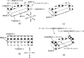
- FIG. 1 A perspective view (a) showing the booster antenna, a perspective view (b) when the booster antenna is viewed in plan, a perspective view (c) of the booster antenna showing a state where the extension is attached, and a communication IC unit mounted with the booster antenna
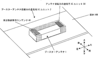
- FIG. A perspective view showing a structure of an antenna-mounted communication IC unit The perspective view which shows the state which installed the communication IC unit of a booster antenna mounting type on the conductor Perspective view (a) and right side view (b) showing another configuration example of the booster antenna Equivalent circuit diagram of communication IC unit with booster antenna
- the booster antenna 1 is roughly composed of a base material 10, a coil 20 of less than one turn, an installation part 30, and a frequency adjusting capacitor 40.
- an insulating plate such as ceramics, mica, and glass, an insulating film, an insulating sheet, an insulating film, etc. are used in addition to any insulating plastic resin that is generally used, such as epoxy resin and polyimide resin. can do. Ceramics are suitable from the viewpoints of insulation, miniaturization, and high temperature resistance.
- a multilayer printed board may be used as the substrate 10.
- the dimension and shape of the base material 10 are not specifically limited, in this Embodiment, it is set as the rectangular parallelepiped shape whose external dimension is about 2 mm long x 5 mm wide x 2 mm in height. That is, a rectangular parallelepiped shape of 5 mm or less ⁇ 5 mm or less ⁇ 2 mm or less in height is preferable.
- the coil 20 having less than one turn is formed by the upper surface side conductor 21, the lower surface side conductor 22 and the connection conductor 23.
- the coil 20 having less than one turn is made of any conductive material including a metal, and can be formed on the base material 10 by a technique such as plating, printing, etching, or vapor deposition. Alternatively, a coil 20 having less than one turn may be formed by cutting out a metal thin plate. As will be described in detail later, the coil 20 having less than one turn constitutes the sub-antenna portion 63.
- the upper surface side conductor 21 is a member attached to the upper surface side of the base material 10.
- the upper surface side conductor 21 of the present embodiment is substantially L-shaped that bends rightward from the entire rear surface of the upper surface of the base material 10 to the front.
- the lower surface side conductor 22 is a member attached to the lower surface side of the base material 10.
- the lower surface side conductor 22 of the present embodiment is attached to the entire front surface of the lower surface of the base material 10, so that the upper surface side conductor 21 and the lower surface side conductor 22 are viewed in plan view from above as shown in FIG. It is preferable to form so as not to overlap.
- the upper surface side conductor 21 and the lower surface side conductor 22 may partially overlap each other.
- the connecting conductor 23 is a member for electrically connecting the end of the upper surface side conductor 21 and the lower surface side conductor 22.
- the installation portion 30 is a location for installing the antenna-mounted communication IC unit 50 and is provided on the upper surface side of the base material 10. In the present embodiment, the installation portion 30 is provided above the bent portion of the upper surface side conductor 21.
- the frequency adjusting capacitor 40 is connected to both ends of the coil 20 having less than one turn.
- an extension 25 (FIG. 1C) is formed from the end of the lower conductor 22 to the upper surface through the side surface of the substrate 10.
- one of the frequency adjustment capacitors 40 is connected to the upper surface side conductor 21 and the other is connected to the extension portion 25, whereby the frequency adjustment capacitor 40 is connected to both ends of the coil 20 having less than one turn.
- the function of the frequency adjusting capacitor 40 will be described later.
- the antenna-mounted communication IC unit 50 includes at least a main antenna unit 60 and an IC chip 70.
- the booster antenna 1 and the antenna-mounted communication IC unit 50 constitute a booster antenna-mounted communication IC unit 2.
- the main antenna unit 60 a plurality of coils 61 are connected in series so that the generation directions of magnetic flux coincide.
- the main antenna unit 60 includes a coil 61 on the back surface (lower surface) of the laminated substrate 62.
- the number of substrates 62 can be adjusted as appropriate, three substrates are used in the present embodiment.
- the substrate 62 in the present embodiment is configured by stacking an intermediate layer substrate 62 and a lowermost layer substrate 62 on the uppermost layer substrate 62 described above.
- the substrate 62 can be laminated by a known method such as a method using an adhesive or a fusion of a resin contained in the substrate 62.
- An uppermost layer coil 61 is formed between the intermediate layer substrate 62 and the uppermost layer substrate 62, and an intermediate layer coil 61 is formed between the intermediate layer substrate 62 and the lowermost layer substrate 62. Is done.
- an insulating plate such as ceramics, mica, and glass, an insulating film, an insulating sheet, an insulating film, etc. are used in addition to any generally used insulating plastic resin including epoxy resin and polyimide resin. be able to. Ceramics are suitable from the viewpoints of insulation, miniaturization, and high temperature resistance.
- substrate 31 are not specifically limited.
- the shape of the substrate 31 can be a rectangular shape such as a square or a rectangle, a circle, an ellipse, or the like.
- the dimension of one side (or the maximum outer shape) of the substrate 31 can be 0.5 mm or more, and preferably 1 mm or more.
- the dimension of one side (or the maximum outer shape) of the substrate 31 can be 8 mm or less, preferably 6 mm or less, more preferably 5 mm or less, and most preferably 3 mm or less.
- the planar outer dimensions are 5 mm ⁇ 5 mm or less.
- an insulating film may be disposed between the substrates 31 as necessary.
- substrate 62 are not specifically limited. Further, an insulating film may be disposed between the substrates 62 as necessary.
- the coil 61 is a so-called planar coil that is spiral in a plane.
- the outermost end of the uppermost coil 61 is connected to one line 71 of the IC chip 70 via a connection point 62 a (through hole) of the uppermost substrate 62. From the outer peripheral end, it turns counterclockwise in a spiral shape, and the inner peripheral end is connected to the inner peripheral end of the intermediate layer coil 61 via a connection point 62 a of the intermediate layer substrate 62.
- the coil 61 of the intermediate layer is spirally counterclockwise from the inner peripheral end thereof, and the outer peripheral end is connected to the other line 71 via a connection point 62 a between the intermediate layer and the uppermost substrate 62.
- the coils 61 are connected in series so that the magnetic flux generated by the common current is generated in the same direction.
- the number of coils 61, the formation area, and the number of turns can be arbitrarily set according to the required inductance of the antenna-mounted communication IC unit 50.
- the number of turns of the coil 61 of the uppermost layer and the intermediate layer is preferably 2 or more, and can be 3 or 4 or more.
- the winding direction and connection form of each coil 61 may be any form other than that shown in the drawing as long as the magnetic field generation direction from each coil 61 is the same direction.
- the coil 61 is formed on the back surface (lower surface) of the substrate 62, but may be formed on the front surface (upper surface) of the substrate 62.
- the coil 61 is made of any conductive material including metal, and can be formed on the substrate 62 by a technique such as plating, printing, etching, or vapor deposition.
- the IC chip 70 is connected to the main antenna unit 60 and is arranged on the upper surface of the uppermost substrate 62 in the present embodiment.
- the IC chip 70 rectifies a part of the carrier wave transmitted from the reader / writer and generates a power supply voltage necessary for operation.
- the generated power supply voltage operates a memory in which a control logic circuit or the like in the IC chip 70 is stored, a communication circuit for transmitting / receiving data to / from the reader / writer, and the like.
- Two lines 71 are drawn from the side surface of the IC chip 70. 1D and 3 show a state in which the surface of the uppermost substrate 62 and the IC chip 70 are covered with a protective layer.
- the main antenna unit 60 is installed in the installation unit 30 as a component of the antenna-mounted communication IC unit 50.
- the main antenna unit 60 and the sub antenna unit 63 are electromagnetically coupled so that the magnetic flux generation direction of the main antenna unit 60 matches the magnetic flux generation direction of the sub antenna unit 63 (the coil 20 of less than one turn).
- the lower surface side conductor 22 constituting the sub antenna part 63 is electrically connected to the conductor 100. That is, the lower surface side conductor 22 is electrically connected to the conductor 100 by bringing the lower surface side of the booster antenna 1 into contact with the conductor 100, whereby the sub-antenna portion 63 (the coil 20 of less than one turn) is electrically connected to the conductor 100. Will be connected to.
- the main antenna unit 60 and the sub antenna unit 63 are connected so that the magnetic flux generation directions of the two coincide with each other, and the sub antenna unit 63 is further connected to the conductor 100 so that the entire conductor 100 is used as an antenna. Can do.
- the conductor 23 for a connection shall be attached to the side surface of the base material 10, you may decide to attach to the inside of the base material 10.
- FIG. 4A if the base material 10 is a multilayer printed circuit board 64 and the connection conductor 23 is passed through the through holes 80 penetrating each layer, the connection conductor 23 becomes the surface of the base material 10. Since it is not exposed to light, the possibility of breakage is reduced and durability can be improved.
- FIG. 4 (b) the connection conductor 23 is extended in an oblique direction from the rear of the upper surface of the base material 10 to the front of the lower surface of the base material 10, thereby connecting the connection conductor 23 to the base material. Compared with the case where it is attached to the side surface of the coil 10, the total length of the coil 20 of less than one turn becomes longer. Thereby, communication performance can be improved more.
- FIG. 5 is an equivalent circuit diagram of the booster antenna-mounted communication IC unit 2 of the present embodiment.
- the main antenna unit 60 and the sub antenna unit 63 constitute a resonance circuit by the equivalent capacitance in the IC chip 70 and the equivalent capacitance including the gap of the open portion 24 of the coil 20 of less than one turn and the frequency adjusting capacitor 40.
- the frequency adjusting capacitor 40 By using the frequency adjusting capacitor 40, the dimensions (mainly the length in the left-right direction) of the booster antenna 1 can be shortened.
- the booster antenna 1 may not include the frequency adjustment capacitor 40.
- the resonance frequency f [Hz] of this resonance circuit is given by equation (1).
- the value of the resonance frequency f is set so as to be included in the frequency band of the radio wave transmitted from the reading device.
- L Inductance of the coil 20 of less than one turn
- C Capacitance of the frequency adjusting capacitor 40
- ⁇ C Electric capacity between conductors in the base material 10 (dielectric) of the booster antenna 1.
- the inductance is proportional to the number of turns of the coil 61. Under the condition that the total number of turns of the coil 61 constituting the main antenna unit 60 is n (where n >> 1), the inductance is increased before and after the main antenna unit 60 and the sub antenna unit 63 are electromagnetically joined. The change is negligible.
- less than one turn of the sub antenna part 63 viewed from the n turns of the main antenna part 60 is less than 1 turn / n turn, so that a change in impedance when attached to the conductor 100 can be reduced. If the n-turn side is viewed from less than one turn, the converted electromagnetic field is multiplied by n from the conductor 100, so that electromagnetic waves can be taken in efficiently. Therefore, if conjugate matching is maintained between the IC chip 70 and the main antenna unit 60, sufficient communication performance can be maintained even after the main antenna unit 60 and the sub antenna unit 63 are electromagnetically joined.
- the base material 10 corresponds to a “base material”
- the upper surface side conductor 21 corresponds to a “first surface side conductor”
- the lower surface side conductor 22 corresponds to a “second surface side conductor”.
- the conductor 23 corresponds to the “connecting conductor”
- the coil portion 20 of less than one turn corresponds to the “coil portion of less than one turn”
- the installation portion 30 corresponds to the “installation portion”
- the booster antenna 1 corresponds to the “booster booster”.
- the extension 25 corresponds to "extension”
- the frequency adjusting capacitor 40 corresponds to “frequency adjusting capacitor”
- the multilayer printed circuit board 64 corresponds to "multilayer printed circuit board”
- the through hole 80 corresponds to a “through hole”
- the booster antenna-mounted communication IC unit 2 corresponds to a “booster antenna-mounted communication IC unit”
- the main antenna portion 60 corresponds to a “main antenna portion”.
- the IC chip 70 corresponds to an “IC chip”
- the conductor 100 corresponds to a “conductor”.
- the present invention is a booster antenna that exhibits high communication performance when mounted on a conductor, a communication IC unit equipped with a booster antenna, and a communication IC unit equipped with a booster antenna with a conductor.
Abstract
[Problem] To provide a booster antenna that exhibits high communication performance when attached to a conductor, a communication IC unit equipped with a booster antenna, and a communication IC unit equipped with a booster antenna having an attached conductor. [Solution] A booster antenna 1 according to the present invention is provided with: a coil 20 that is wound less than one turn and that is formed of an upper-surface-side conductor 21 attached to an upper surface side of a substrate 10, a lower-surface-side conductor 22 attached to a lower surface side of the substrate, and a connection conductor 23 attached to an interior or a lateral surface of the substrate to electrically connect an end section of the upper-surface-side conductor and an end section of the lower-surface-side conductor; and an installation section 30 for installing a communication IC unit 50 equipped with an antenna on the upper surface side of the substrate. When the lower-surface-side conductor and a conductor are electrically contacted and connected, a conductor 100 functions as an antenna.
Description
本発明は、導体に取り付けた場合に高い通信性能を発揮するブースターアンテナ、ブースターアンテナ搭載形の通信用ICユニット、及び導体付きブースターアンテナ搭載形の通信用ICユニットを提供することを目的とする。
An object of the present invention is to provide a booster antenna that exhibits high communication performance when attached to a conductor, a booster antenna-mounted communication IC unit, and a conductor-mounted booster antenna-mounted communication IC unit.
近年、RFID(Radio Frequency Identification)が利用されている。
RFIDシステムで使用するRFタグにはアンテナ及びICチップが格納されており、リーダ・ライタのアンテナから送信された搬送波をRFタグのアンテナで受信し、ICチップに記録されている識別データ等を反射波に乗せてリーダ・ライタへ返送することで非接触で交信する仕組みになっている。 In recent years, RFID (Radio Frequency Identification) has been used.
The RF tag used in the RFID system contains an antenna and an IC chip. The carrier wave transmitted from the reader / writer antenna is received by the RF tag antenna and the identification data recorded on the IC chip is reflected. It communicates in a non-contact manner by returning it to the reader / writer on the wave.
従来のRFタグ用のアンテナとして例えば二次元の一層の渦巻状のタイプが知られている。しかし、パターンサイズを小さくして高インダクタンスを実現することが難しいため、回路設計が難しいという問題または、ICチップに搭載して小型化するのが難しいという問題があった。
そこで、本願発明者は、コイルを形成した基板を積層すると共に磁界の発生方向が同一方向になるように各コイルを直列接続したアンテナ搭載形の通信用ICユニットを開発した(特許文献1及び2)。
このICユニットによれば、積層した複数のコイルを一体的に作動させることができるので、高インダクタンスを実現でき、回路設計及び小型化が容易になる。 As a conventional antenna for an RF tag, for example, a two-dimensional one-layer spiral type is known. However, since it is difficult to realize a high inductance by reducing the pattern size, there has been a problem that circuit design is difficult, or that it is difficult to reduce the size by mounting on an IC chip.
Accordingly, the inventor of the present application has developed an antenna-mounted communication IC unit in which the coils are stacked and the coils are connected in series so that the magnetic field is generated in the same direction (Patent Documents 1 and 2). ).
According to this IC unit, a plurality of stacked coils can be operated integrally, so that high inductance can be realized, and circuit design and miniaturization are facilitated.
ところが、上記従来技術では以下のような問題がある。
すなわち、通信距離が短いためリーダ・ライタをICユニットの近傍まで近づける必要があるという問題がある。
また、ICユニットを導体(金属物等)に近づけると共振周波数がずれてしまい通信に支障が出るという問題または、ICユニットを取り付けた面の裏側の面に電波を照射した場合には通信できないという問題がある。 However, the prior art has the following problems.
That is, since the communication distance is short, it is necessary to bring the reader / writer close to the vicinity of the IC unit.
In addition, if the IC unit is brought closer to a conductor (metal object, etc.), the resonance frequency will shift and this will interfere with communication, or communication will not be possible if radio waves are irradiated on the back side of the surface where the IC unit is attached. There's a problem.
本発明は、このような問題を考慮して、導体に取り付けた場合に高い通信性能を発揮するブースターアンテナ、ブースターアンテナ搭載形の通信用ICユニット、及び導体付きブースターアンテナ搭載形の通信用ICユニットを提供することを目的とする。
In consideration of such problems, the present invention provides a booster antenna that exhibits high communication performance when mounted on a conductor, a booster antenna-mounted communication IC unit, and a conductor-mounted booster antenna-mounted communication IC unit. The purpose is to provide.
本発明のブースターアンテナは、基材の上面側に取り付けられる上面側導体、基材の下面側に取り付けられる下面側導体、基材の内部又は側面に取り付けられて上面側導体の端部と下面側導体の端部とを電気的に接続する接続用導体によって形成される1ターン未満のコイルと、基材の上面側にアンテナ搭載形の通信用ICユニットを設置するための設置部とを備えることを特徴とする。
また、アンテナ搭載形の通信用ICユニットが、磁束の発生方向が一致するように複数のコイルが直列接続されて成る主アンテナ部と、当該主アンテナ部と接続されるICチップとを少なくとも備えており、1ターン未満のコイルが副アンテナ部を構成しており、主アンテナ部の磁束の発生方向と副アンテナ部の磁束の発生方向が一致するように主アンテナ部と副アンテナ部が電磁結合されることを特徴とする。
また、1ターン未満のコイルの両端部に周波数調整用コンデンサが接続されていることを特徴とする。
また、平面視した場合に、上面側導体と下面側導体とが重ならないように取り付けられていることを特徴とする。
また、基材が多層プリント基板であり、接続用導体が当該多層プリント基板の各層を貫通するスルーホール内を通って上面側導体と下面側導体とを電気的に接続することを特徴とする。 The booster antenna of the present invention includes an upper surface side conductor attached to the upper surface side of the base material, a lower surface side conductor attached to the lower surface side of the base material, and an end portion and a lower surface side of the upper surface side conductor attached to the inside or the side surface of the base material. A coil of less than one turn formed by a connecting conductor that electrically connects the end of the conductor, and an installation part for installing the antenna-mounted communication IC unit on the upper surface side of the base material It is characterized by.
Moreover, the antenna-mounted communication IC unit includes at least a main antenna unit in which a plurality of coils are connected in series so that the magnetic flux generation directions coincide with each other, and an IC chip connected to the main antenna unit. The coil of less than one turn constitutes the sub antenna part, and the main antenna part and the sub antenna part are electromagnetically coupled so that the magnetic flux generation direction of the main antenna part coincides with the magnetic flux generation direction of the sub antenna part. It is characterized by that.
Further, a frequency adjusting capacitor is connected to both ends of the coil of less than one turn.
Further, when viewed in a plan view, the upper surface side conductor and the lower surface side conductor are attached so as not to overlap each other.
Further, the base material is a multilayer printed board, and the connecting conductor electrically connects the upper surface side conductor and the lower surface side conductor through the through-hole penetrating each layer of the multilayer printed board.
本発明のブースターアンテナの使用方法は、上記ブースターアンテナの使用方法において、下面側導体と導体とを電気的に接触接続させることを特徴とする。
本発明のブースターアンテナ搭載形の通信用ICユニットは、上記ブースターアンテナと、アンテナ搭載形の通信用ICユニットとを備えており、アンテナ搭載形の通信用ICユニットが、磁束の発生方向が一致するように複数のコイルが直列接続されて成る主アンテナ部と、当該主アンテナ部と接続されるICチップとを少なくとも備えており、1ターン未満のコイルが副アンテナ部を構成しており、主アンテナ部と副アンテナ部とが電磁結合されることを特徴とする。 The method of using the booster antenna according to the present invention is characterized in that, in the method of using the booster antenna, the lower surface side conductor and the conductor are electrically contact-connected.
The booster antenna-mounted communication IC unit of the present invention includes the booster antenna and the antenna-mounted communication IC unit, and the antenna-mounted communication IC unit has the same magnetic flux generation direction. A plurality of coils connected in series, and an IC chip connected to the main antenna unit, and a coil of less than one turn constitutes a sub-antenna unit. The portion and the sub-antenna portion are electromagnetically coupled.
本発明では主アンテナ部と副アンテナ部を共にコイルで構成し、導体に設置する副エレメントのコイル形状を1ターン未満とする。そして、主アンテナ部と副アンテナ部を両者の磁束の発生方向が一致するように接続することで導体全体をアンテナとして機能させる。
ICユニットから離れた位置からリーダ・ライタの搬送波を送信した場合、搬送波がICユニットまで届かない場合がある。しかし、本発明では導体がアンテナとして機能するため、搬送波が導体の一部まで届きさえすれば、搬送波は導体を伝わり副アンテナ部及び主アンテナ部まで至り、ICチップにおいて電源電圧が生成され、通信回路等を動作させることができる。
また、本発明ではICユニットを取り付けた面の裏側の面に電波を照射した場合にも、表側の面に電波を照射した場合とほぼ同品質で通信できる。
このように、本発明のブースターアンテナ、ブースターアンテナ搭載形の通信用ICユニット、及び導体付きブースターアンテナ搭載形の通信用ICユニットは導体に取り付けた場合に高い通信性能を発揮することができる。
なお、本発明において「導体」とは一般的な意味と同様に「電気の伝導率が比較的大きな物質の総称」(広辞苑)であり、例えば金属、炭素繊維、人体、動物の体、草木、水、地面などが挙げられるが、必ずしもこれらに限定されない。 In the present invention, the main antenna portion and the sub antenna portion are both constituted by coils, and the coil shape of the sub element installed on the conductor is less than one turn. Then, the entire conductor functions as an antenna by connecting the main antenna unit and the sub-antenna unit so that the magnetic flux generation directions of the two match.
When the carrier wave of the reader / writer is transmitted from a position away from the IC unit, the carrier wave may not reach the IC unit. However, in the present invention, since the conductor functions as an antenna, if the carrier wave reaches a part of the conductor, the carrier wave propagates through the conductor to the sub-antenna part and the main antenna part, and a power supply voltage is generated in the IC chip. A circuit or the like can be operated.
Further, in the present invention, even when a radio wave is irradiated on the back surface of the surface where the IC unit is attached, communication can be performed with substantially the same quality as when a radio wave is irradiated on the front surface.
As described above, the booster antenna, the booster antenna mounted communication IC unit, and the booster antenna mounted communication IC unit of the present invention can exhibit high communication performance when attached to a conductor.
In the present invention, the term “conductor” is “generic name for substances having a relatively large electrical conductivity” (Kojien), as well as the general meaning. For example, metal, carbon fiber, human body, animal body, vegetation, Although water, the ground, etc. are mentioned, it is not necessarily limited to these.
また、本発明では複数のコイルを直列接続することで主アンテナ部を構成するので小型化が可能になる。
また、1ターン未満のコイルの両端部に周波数調整用コンデンサを接続することによっても小型化が可能になる。
また、平面視した場合に上面側導体と下面側導体とが重ならないように両者を基材に取り付けることにすれば、平面視した場合に1ターン未満のコイルのコイルがC字状になる。これにより下面側導体を導体に対して電気的に接触接続させない場合であっても、基材の上面に対して直交する方向からの搬送波に対してブースターアンテナ搭載形の通信用ICユニット単独で送受信が可能になる。
また、基材を多層プリント基板として各層を貫通するスルーホールに接続用導体を通すことにすれば、接続用導体が基材の表面に露出しないので破損の可能性が少なくなり、耐久性を向上させることができる。 Further, in the present invention, the main antenna portion is configured by connecting a plurality of coils in series, so that the size can be reduced.
The size can also be reduced by connecting frequency adjusting capacitors to both ends of the coil of less than one turn.
Moreover, if both are attached to a base material so that an upper surface side conductor and a lower surface side conductor may not overlap when seen in a plan view, a coil of less than one turn becomes C-shaped when seen in a plan view. Thus, even when the lower surface side conductor is not electrically connected to the conductor, the booster antenna-mounted communication IC unit alone transmits and receives the carrier wave from the direction orthogonal to the upper surface of the base material. Is possible.
If the base material is a multilayer printed circuit board and the connection conductor is passed through the through-holes that pass through each layer, the connection conductor will not be exposed on the surface of the base material, reducing the possibility of damage and improving durability. Can be made.
本発明のブースターアンテナ、ブースターアンテナ搭載形の通信用ICユニット、及び導体付きブースターアンテナ搭載形の通信用ICユニットの実施の形態について図面を用いて説明する。
図1に示すようにブースターアンテナ1は基材10、1ターン未満のコイル20、設置部30、周波数調整用コンデンサ40から概略構成される。 Embodiments of a booster antenna, a booster antenna-mounted communication IC unit, and a conductor-mounted booster antenna-mounted communication IC unit according to the present invention will be described with reference to the drawings.
As shown in FIG. 1, the booster antenna 1 is roughly composed of a base material 10, a coil 20 of less than one turn, an installation part 30, and a frequency adjusting capacitor 40.
基材10としては一般的に使用される例えばエポキシ樹脂、ポリイミド樹脂を含む任意の絶縁性のプラスチック樹脂の他、セラミックス、マイカ、ガラスなどの絶縁板、絶縁フィルム、絶縁シート、絶縁膜等を使用することができる。絶縁性、小型化、耐高温性の観点ではセラミックスが適している。基材10として多層プリント基板を使用してもよい。
なお、基材10の寸法及び形状は特に限定されないが、本実施の形態では外形寸法が縦2mm×横5mm×高さ2mm程度の直方体形状とする。すなわち、縦5mm以下×横5mm以下×高さ2mm以下の直方体形状であることが好ましい。 As the base material 10, for example, an insulating plate such as ceramics, mica, and glass, an insulating film, an insulating sheet, an insulating film, etc. are used in addition to any insulating plastic resin that is generally used, such as epoxy resin and polyimide resin. can do. Ceramics are suitable from the viewpoints of insulation, miniaturization, and high temperature resistance. A multilayer printed board may be used as the substrate 10.
In addition, although the dimension and shape of the base material 10 are not specifically limited, in this Embodiment, it is set as the rectangular parallelepiped shape whose external dimension is about 2 mm long x 5 mm wide x 2 mm in height. That is, a rectangular parallelepiped shape of 5 mm or less × 5 mm or less × 2 mm or less in height is preferable.
1ターン未満のコイル20は上面側導体21、下面側導体22及び接続用導体23によって形成される。1ターン未満のコイル20は金属を含む任意の導電性材料から成り、基材10に対してメッキ、印刷、エッチング、蒸着等の手法によって形成することができる。あるいは、金属の薄板を切り抜いて1ターン未満のコイル20を形成してもよい。詳しい説明は後述するが1ターン未満のコイル20が副アンテナ部63を構成することになる。
上面側導体21は基材10の上面側に取り付けられる部材である。本実施の形態の上面側導体21は基材10上面の後方全体から右側で屈曲して前方に至るほぼL字状になっている。
下面側導体22は基材10の下面側に取り付けられる部材である。本実施の形態の下面側導体22は基材10下面の前方全体に取り付けられており、これにより図1(b)に示すように上方から平面視した場合に上面側導体21と下面側導体22とが重ならないように形成することが好ましい。なお、上面側導体21と下面側導体22とが一部重なっていてもよい。
接続用導体23は上面側導体21の端部と下面側導体22とを電気的に接続するための部材である。本実施の形態では基材10の側面(前面)の右側に取り付けられる。
このように、上面側導体21と下面側導体22の一方の端部同士を接続用導体23で接続することで、図1(a)及び(b)に示すように上面側導体21と下面側導体22の他方の端部間は開放部24となる。また、設置部30全体として1ターン未満のコイル20を形成している。
設置部30はアンテナ搭載形の通信用ICユニット50を設置するための箇所であり、基材10の上面側に設けられる。本実施の形態では上面側導体21の屈曲箇所の上方に設置部30を設けてある。 The coil 20 having less than one turn is formed by the upper surface side conductor 21, the lower surface side conductor 22 and the connection conductor 23. The coil 20 having less than one turn is made of any conductive material including a metal, and can be formed on the base material 10 by a technique such as plating, printing, etching, or vapor deposition. Alternatively, a coil 20 having less than one turn may be formed by cutting out a metal thin plate. As will be described in detail later, the coil 20 having less than one turn constitutes the sub-antenna portion 63.
The upper surface side conductor 21 is a member attached to the upper surface side of the base material 10. The upper surface side conductor 21 of the present embodiment is substantially L-shaped that bends rightward from the entire rear surface of the upper surface of the base material 10 to the front.
The lower surface side conductor 22 is a member attached to the lower surface side of the base material 10. The lower surface side conductor 22 of the present embodiment is attached to the entire front surface of the lower surface of the base material 10, so that the upper surface side conductor 21 and the lower surface side conductor 22 are viewed in plan view from above as shown in FIG. It is preferable to form so as not to overlap. The upper surface side conductor 21 and the lower surface side conductor 22 may partially overlap each other.
The connecting conductor 23 is a member for electrically connecting the end of the upper surface side conductor 21 and the lower surface side conductor 22. In this Embodiment, it attaches to the right side of the side surface (front surface) of the base material 10. FIG.
In this way, by connecting one end of the upper surface side conductor 21 and the lower surface side conductor 22 with the connecting conductor 23, the upper surface side conductor 21 and the lower surface side as shown in FIGS. 1 (a) and 1 (b). An opening 24 is provided between the other ends of the conductor 22. Moreover, the coil 20 of less than 1 turn is formed as the installation part 30 whole.
The installation portion 30 is a location for installing the antenna-mounted communication IC unit 50 and is provided on the upper surface side of the base material 10. In the present embodiment, the installation portion 30 is provided above the bent portion of the upper surface side conductor 21.
図1(d)に示すように、周波数調整用コンデンサ40は1ターン未満のコイル20の両端部に接続されている。具体的には下面側導体22の端部から基材10の側面を通って上面に至る延長部25(図1(c))が形成されている。そして、周波数調整用コンデンサ40の一方を上面側導体21に接続し、他方を延長部25に接続することで周波数調整用コンデンサ40が1ターン未満のコイル20の両端部に接続されることになる。周波数調整用コンデンサ40の機能については後述する。
As shown in FIG. 1D, the frequency adjusting capacitor 40 is connected to both ends of the coil 20 having less than one turn. Specifically, an extension 25 (FIG. 1C) is formed from the end of the lower conductor 22 to the upper surface through the side surface of the substrate 10. Then, one of the frequency adjustment capacitors 40 is connected to the upper surface side conductor 21 and the other is connected to the extension portion 25, whereby the frequency adjustment capacitor 40 is connected to both ends of the coil 20 having less than one turn. . The function of the frequency adjusting capacitor 40 will be described later.
図2に示すようにアンテナ搭載形の通信用ICユニット50は主アンテナ部60とICチップ70とを少なくとも備えている。図1(d)に示すように上記ブースターアンテナ1と、アンテナ搭載形の通信用ICユニット50とによってブースターアンテナ搭載形の通信用ICユニット2を構成している。
主アンテナ部60は磁束の発生方向が一致するように複数のコイル61が直列接続されている。
具体的には、主アンテナ部60は積層した基板62の裏面(下面)にコイル61を備えている。基板62の枚数は適宜調節可能であるが、本実施の形態では3枚使用している。
本実施の形態における基板62は、上述した最上層の基板62に、中間層の基板62、最下層の基板62を積層して構成される。基板62を積層するには、接着剤を用いる方法、基板62に含まれる樹脂の融着など公知の方法によって行うことができる。
中間層の基板62と最上層の基板62との間には、最上層のコイル61が形成され、中間層の基板62と最下層の基板62との間には、中間層のコイル61が形成される。
基板62としては一般的に使用される例えばエポキシ樹脂、ポリイミド樹脂を含む任意の絶縁性のプラスチック樹脂の他、セラミックス、マイカ、ガラスなどの絶縁板、絶縁フィルム、絶縁シート、絶縁膜等を使用することができる。絶縁性、小型化、耐高温性の観点ではセラミックスが適している。
なお、基板31の寸法及び形状は特に限定されない。例えば、基板31の形状は正方形、長方形などの矩形状、円形、楕円形などとすることができる。基板31の一辺(または最大外形)の寸法は0.5mm以上とすることができ、1mm以上が好ましい。また、基板31の一辺(または最大外形)の寸法は8mm以下とすることができ、6mm以下が好ましく、5mm以下がより好ましく、3mm以下が最も好ましい。本実施の形態では平面外形寸法が5mm×5mm以下とする。また、各基板31の間に必要に応じて絶縁膜を配置してもよい。
なお、基板62の寸法及び形状は特に限定されない。また、各基板62の間に必要に応じて絶縁膜を配置してもよい。 As shown in FIG. 2, the antenna-mounted communication IC unit 50 includes at least a main antenna unit 60 and an IC chip 70. As shown in FIG. 1D, the booster antenna 1 and the antenna-mounted communication IC unit 50 constitute a booster antenna-mounted communication IC unit 2.
In the main antenna unit 60, a plurality of coils 61 are connected in series so that the generation directions of magnetic flux coincide.
Specifically, the main antenna unit 60 includes a coil 61 on the back surface (lower surface) of the laminated substrate 62. Although the number of substrates 62 can be adjusted as appropriate, three substrates are used in the present embodiment.
The substrate 62 in the present embodiment is configured by stacking an intermediate layer substrate 62 and a lowermost layer substrate 62 on the uppermost layer substrate 62 described above. The substrate 62 can be laminated by a known method such as a method using an adhesive or a fusion of a resin contained in the substrate 62.
An uppermost layer coil 61 is formed between the intermediate layer substrate 62 and the uppermost layer substrate 62, and an intermediate layer coil 61 is formed between the intermediate layer substrate 62 and the lowermost layer substrate 62. Is done.
As the substrate 62, an insulating plate such as ceramics, mica, and glass, an insulating film, an insulating sheet, an insulating film, etc. are used in addition to any generally used insulating plastic resin including epoxy resin and polyimide resin. be able to. Ceramics are suitable from the viewpoints of insulation, miniaturization, and high temperature resistance.
In addition, the dimension and shape of the board | substrate 31 are not specifically limited. For example, the shape of the substrate 31 can be a rectangular shape such as a square or a rectangle, a circle, an ellipse, or the like. The dimension of one side (or the maximum outer shape) of the substrate 31 can be 0.5 mm or more, and preferably 1 mm or more. The dimension of one side (or the maximum outer shape) of the substrate 31 can be 8 mm or less, preferably 6 mm or less, more preferably 5 mm or less, and most preferably 3 mm or less. In this embodiment, the planar outer dimensions are 5 mm × 5 mm or less. Further, an insulating film may be disposed between the substrates 31 as necessary.
In addition, the dimension and shape of the board | substrate 62 are not specifically limited. Further, an insulating film may be disposed between the substrates 62 as necessary.
コイル61は平面内で渦巻状のいわゆる平面コイルである。
最上層のコイル61は、その外周端が最上層の基板62の接続点62a(貫通穴)を介してICチップ70の一方のライン71に接続される。当該外周端から渦巻状に反時計回りとなり、内周端が中間層の基板62の接続点62aを介して中間層のコイル61の内周端に接続される。
中間層のコイル61は、その内周端から渦巻状に反時計回りとなり、外周端が中間層及び最上層の基板62の接続点62aを介して他方のライン71に接続される。 The coil 61 is a so-called planar coil that is spiral in a plane.
The outermost end of the uppermost coil 61 is connected to one line 71 of the IC chip 70 via a connection point 62 a (through hole) of the uppermost substrate 62. From the outer peripheral end, it turns counterclockwise in a spiral shape, and the inner peripheral end is connected to the inner peripheral end of the intermediate layer coil 61 via a connection point 62 a of the intermediate layer substrate 62.
The coil 61 of the intermediate layer is spirally counterclockwise from the inner peripheral end thereof, and the outer peripheral end is connected to the other line 71 via a connection point 62 a between the intermediate layer and the uppermost substrate 62.
上述のとおり各コイル61は共通の電流による磁束の発生方向が同一方向となるように直列接続されている。なお、各コイル61の数、形成面積、ターン数は、アンテナ搭載形の通信用ICユニット50の所要インダクタンスに応じて任意に設定することができる。例えば、最上層および中間層のコイル61の巻き数は2以上とするのがよく、3あるいは4以上とすることができる。また、各コイル61の巻き方向及び接続形態は、各コイル61からの磁界の発生方向が同一方向である限り、図示以外の任意の形態であってもよい。また、本実施の形態ではコイル61を基板62の裏面(下面)に形成するものとしたが、基板62の表面(上面)に形成してもよい。
コイル61は金属を含む任意の導電性材料から成り、基板62に対してメッキ、印刷、エッチング、蒸着等の手法によって形成することができる。 As described above, the coils 61 are connected in series so that the magnetic flux generated by the common current is generated in the same direction. The number of coils 61, the formation area, and the number of turns can be arbitrarily set according to the required inductance of the antenna-mounted communication IC unit 50. For example, the number of turns of the coil 61 of the uppermost layer and the intermediate layer is preferably 2 or more, and can be 3 or 4 or more. The winding direction and connection form of each coil 61 may be any form other than that shown in the drawing as long as the magnetic field generation direction from each coil 61 is the same direction. In this embodiment, the coil 61 is formed on the back surface (lower surface) of the substrate 62, but may be formed on the front surface (upper surface) of the substrate 62.
The coil 61 is made of any conductive material including metal, and can be formed on the substrate 62 by a technique such as plating, printing, etching, or vapor deposition.
ICチップ70は主アンテナ部60と接続されるものであり、本実施の形態では最上層の基板62の上面に配置される。ICチップ70はリーダ・ライタから送信される搬送波の一部を整流し、動作するために必要な電源電圧を生成する。そして、生成した電源電圧によってICチップ70内の制御用の論理回路等が格納されたメモリ、及びリーダ・ライタとのデータの送受信を行うための通信回路等を動作させる。
ICチップ70の側面から2本のライン71を引き出している。なお、図1(d)及び図3では最上層の基板62の表面及びICチップ70を保護層で覆った状態を示している。
主アンテナ部60はアンテナ搭載形の通信用ICユニット50の構成部品として設置部30に設置されている。そして、主アンテナ部60の磁束の発生方向と副アンテナ部63(1ターン未満のコイル20)の磁束の発生方向が一致するように主アンテナ部60と副アンテナ部63が電磁結合される。
また、図3に示すように副アンテナ部63を構成する下面側導体22は導体100と電気的に接触接続される。つまり、ブースターアンテナ1の下面側を導体100に接触させることで下面側導体22が導体100に電気的に接続され、これにより副アンテナ部63(1ターン未満のコイル20)が導体100に電気的に接続されることになる。
このように主アンテナ部60と副アンテナ部63とを両者の磁束の発生方向が一致するように接続し、更に副アンテナ部63を導体100に接続することで導体100全体をアンテナとして利用することができる。 The IC chip 70 is connected to the main antenna unit 60 and is arranged on the upper surface of the uppermost substrate 62 in the present embodiment. The IC chip 70 rectifies a part of the carrier wave transmitted from the reader / writer and generates a power supply voltage necessary for operation. The generated power supply voltage operates a memory in which a control logic circuit or the like in the IC chip 70 is stored, a communication circuit for transmitting / receiving data to / from the reader / writer, and the like.
Two lines 71 are drawn from the side surface of the IC chip 70. 1D and 3 show a state in which the surface of the uppermost substrate 62 and the IC chip 70 are covered with a protective layer.
The main antenna unit 60 is installed in the installation unit 30 as a component of the antenna-mounted communication IC unit 50. The main antenna unit 60 and the sub antenna unit 63 are electromagnetically coupled so that the magnetic flux generation direction of the main antenna unit 60 matches the magnetic flux generation direction of the sub antenna unit 63 (the coil 20 of less than one turn).
Further, as shown in FIG. 3, the lower surface side conductor 22 constituting the sub antenna part 63 is electrically connected to the conductor 100. That is, the lower surface side conductor 22 is electrically connected to the conductor 100 by bringing the lower surface side of the booster antenna 1 into contact with the conductor 100, whereby the sub-antenna portion 63 (the coil 20 of less than one turn) is electrically connected to the conductor 100. Will be connected to.
In this way, the main antenna unit 60 and the sub antenna unit 63 are connected so that the magnetic flux generation directions of the two coincide with each other, and the sub antenna unit 63 is further connected to the conductor 100 so that the entire conductor 100 is used as an antenna. Can do.
なお、上記実施の形態では接続用導体23が基材10の側面に取り付けられるものとしたが、基材10の内部に取り付けられることにしてもよい。
例えば図4(a)に示すように、基材10を多層プリント基板64とし、各層を貫通するスルーホール80に接続用導体23を通すことにすれば、接続用導体23が基材10の表面に露出しないので破損の可能性が少なくなり、耐久性を向上させることができる。
或いは図4(b)に示すように、接続用導体23を基材10上面の後方から基材10下面の前方まで基材10の内部を斜め方向にのばすことにより、接続用導体23を基材10の側面に取り付ける場合と比較して1ターン未満のコイル20の全長が長くなる。これにより通信性能をより高めることができる。 In addition, in the said embodiment, although the conductor 23 for a connection shall be attached to the side surface of the base material 10, you may decide to attach to the inside of the base material 10. FIG.
For example, as shown in FIG. 4A, if the base material 10 is a multilayer printed circuit board 64 and the connection conductor 23 is passed through the through holes 80 penetrating each layer, the connection conductor 23 becomes the surface of the base material 10. Since it is not exposed to light, the possibility of breakage is reduced and durability can be improved.
Alternatively, as shown in FIG. 4 (b), the connection conductor 23 is extended in an oblique direction from the rear of the upper surface of the base material 10 to the front of the lower surface of the base material 10, thereby connecting the connection conductor 23 to the base material. Compared with the case where it is attached to the side surface of the coil 10, the total length of the coil 20 of less than one turn becomes longer. Thereby, communication performance can be improved more.
図5は本実施の形態のブースターアンテナ搭載形の通信用ICユニット2の等価回路図である。主アンテナ部60と副アンテナ部63は、ICチップ70内の等価容量、1ターン未満のコイル20の開放部24の間隙を含む等価容量及び周波数調整用コンデンサ40によって共振回路を構成している。周波数調整用コンデンサ40を用いることでブースターアンテナ1の寸法(主に左右方向の長さ)を短くすることができる。なお、ブースターアンテナ1が周波数調整用コンデンサ40を備えないことにしてもよい。
この共振回路の共振周波数f[Hz]は、式(1)により与えられる。共振周波数fの値は、読取装置から送信される電波の周波数帯域に含まれるように設定される。

L:1ターン未満のコイル20のインダクタンス、C:周波数調整用コンデンサ40の静電容量、εC:ブースターアンテナ1の基材10(誘電体)における導体間の電気容量。
ここで、インダクタンスはコイル61の巻数に比例する。主アンテナ部60を構成するコイル61の総巻数をn(但し、n≫1)とした条件下では、主アンテナ部60と副アンテナ部63とを電磁的に接合させる前と後とでインダクタンスの変化はごく僅かである。つまり、主アンテナ部60のnターンから見た副アンテナ部63の1ターン未満は、1ターン未満/nターンとなるため導体100に取り付けた場合のインピーダンスの変化を少なくすることができ、また、1ターン未満からnターン側を見れば導体100から変換電磁界はn倍されるため効率よく電磁波を取り込むことができる。したがって、ICチップ70と主アンテナ部60との間で共役整合を取っておけば、主アンテナ部60と副アンテナ部63とを電磁的に接合した後でも充分な通信性能を維持できる。 FIG. 5 is an equivalent circuit diagram of the booster antenna-mounted communication IC unit 2 of the present embodiment. The main antenna unit 60 and the sub antenna unit 63 constitute a resonance circuit by the equivalent capacitance in the IC chip 70 and the equivalent capacitance including the gap of the open portion 24 of the coil 20 of less than one turn and the frequency adjusting capacitor 40. By using the frequency adjusting capacitor 40, the dimensions (mainly the length in the left-right direction) of the booster antenna 1 can be shortened. The booster antenna 1 may not include the frequency adjustment capacitor 40.
The resonance frequency f [Hz] of this resonance circuit is given by equation (1). The value of the resonance frequency f is set so as to be included in the frequency band of the radio wave transmitted from the reading device.
L: Inductance of the coil 20 of less than one turn, C: Capacitance of the frequency adjusting capacitor 40, εC: Electric capacity between conductors in the base material 10 (dielectric) of the booster antenna 1.
Here, the inductance is proportional to the number of turns of the coil 61. Under the condition that the total number of turns of the coil 61 constituting the main antenna unit 60 is n (where n >> 1), the inductance is increased before and after the main antenna unit 60 and the sub antenna unit 63 are electromagnetically joined. The change is negligible. That is, less than one turn of the sub antenna part 63 viewed from the n turns of the main antenna part 60 is less than 1 turn / n turn, so that a change in impedance when attached to the conductor 100 can be reduced. If the n-turn side is viewed from less than one turn, the converted electromagnetic field is multiplied by n from the conductor 100, so that electromagnetic waves can be taken in efficiently. Therefore, if conjugate matching is maintained between the IC chip 70 and the main antenna unit 60, sufficient communication performance can be maintained even after the main antenna unit 60 and the sub antenna unit 63 are electromagnetically joined.
この共振回路の共振周波数f[Hz]は、式(1)により与えられる。共振周波数fの値は、読取装置から送信される電波の周波数帯域に含まれるように設定される。
ここで、インダクタンスはコイル61の巻数に比例する。主アンテナ部60を構成するコイル61の総巻数をn(但し、n≫1)とした条件下では、主アンテナ部60と副アンテナ部63とを電磁的に接合させる前と後とでインダクタンスの変化はごく僅かである。つまり、主アンテナ部60のnターンから見た副アンテナ部63の1ターン未満は、1ターン未満/nターンとなるため導体100に取り付けた場合のインピーダンスの変化を少なくすることができ、また、1ターン未満からnターン側を見れば導体100から変換電磁界はn倍されるため効率よく電磁波を取り込むことができる。したがって、ICチップ70と主アンテナ部60との間で共役整合を取っておけば、主アンテナ部60と副アンテナ部63とを電磁的に接合した後でも充分な通信性能を維持できる。 FIG. 5 is an equivalent circuit diagram of the booster antenna-mounted communication IC unit 2 of the present embodiment. The main antenna unit 60 and the sub antenna unit 63 constitute a resonance circuit by the equivalent capacitance in the IC chip 70 and the equivalent capacitance including the gap of the open portion 24 of the coil 20 of less than one turn and the frequency adjusting capacitor 40. By using the frequency adjusting capacitor 40, the dimensions (mainly the length in the left-right direction) of the booster antenna 1 can be shortened. The booster antenna 1 may not include the frequency adjustment capacitor 40.
The resonance frequency f [Hz] of this resonance circuit is given by equation (1). The value of the resonance frequency f is set so as to be included in the frequency band of the radio wave transmitted from the reading device.
Here, the inductance is proportional to the number of turns of the coil 61. Under the condition that the total number of turns of the coil 61 constituting the main antenna unit 60 is n (where n >> 1), the inductance is increased before and after the main antenna unit 60 and the sub antenna unit 63 are electromagnetically joined. The change is negligible. That is, less than one turn of the sub antenna part 63 viewed from the n turns of the main antenna part 60 is less than 1 turn / n turn, so that a change in impedance when attached to the conductor 100 can be reduced. If the n-turn side is viewed from less than one turn, the converted electromagnetic field is multiplied by n from the conductor 100, so that electromagnetic waves can be taken in efficiently. Therefore, if conjugate matching is maintained between the IC chip 70 and the main antenna unit 60, sufficient communication performance can be maintained even after the main antenna unit 60 and the sub antenna unit 63 are electromagnetically joined.
本発明において、基材10が「基材」に相当し、上面側導体21が「第1面側導体」に相当し、下面側導体22が「第2面側導体」に相当し、接続用導体23が「接続用導体」に相当し、1ターン未満のコイル部20が「1ターン未満のコイル部」に相当し、設置部30が「設置部」に相当し、ブースターアンテナ1が「ブースターアンテナ」に相当し、延長部25が「延長部」に相当し、周波数調整用コンデンサ40が「周波数調整用コンデンサ」に相当し、多層プリント基板64が「多層プリント基板」に相当し、
スルーホール80が「スルーホール」に相当し、ブースターアンテナ搭載形の通信用ICユニット2が「ブースターアンテナ搭載形の通信用ICユニット」に相当し、主アンテナ部60が「主アンテナ部」に相当し、ICチップ70が「ICチップ」に相当し、導体100が「導体」に相当する。 In the present invention, the base material 10 corresponds to a “base material”, the upper surface side conductor 21 corresponds to a “first surface side conductor”, and the lower surface side conductor 22 corresponds to a “second surface side conductor”. The conductor 23 corresponds to the “connecting conductor”, the coil portion 20 of less than one turn corresponds to the “coil portion of less than one turn”, the installation portion 30 corresponds to the “installation portion”, and the booster antenna 1 corresponds to the “booster booster”. It corresponds to "antenna", the extension 25 corresponds to "extension", the frequency adjusting capacitor 40 corresponds to "frequency adjusting capacitor", the multilayer printed circuit board 64 corresponds to "multilayer printed circuit board",
The through hole 80 corresponds to a “through hole”, the booster antenna-mounted communication IC unit 2 corresponds to a “booster antenna-mounted communication IC unit”, and the main antenna portion 60 corresponds to a “main antenna portion”. The IC chip 70 corresponds to an “IC chip”, and the conductor 100 corresponds to a “conductor”.
本発明は、導体に取り付けた場合に高い通信性能を発揮するブースターアンテナ、ブースターアンテナ搭載形の通信用ICユニット、及び導体付きブースターアンテナ搭載形の通信用ICユニットであり、産業上の利用可能性を有する。
INDUSTRIAL APPLICABILITY The present invention is a booster antenna that exhibits high communication performance when mounted on a conductor, a communication IC unit equipped with a booster antenna, and a communication IC unit equipped with a booster antenna with a conductor. Have
1 ブースターアンテナ
2 ブースターアンテナ搭載形の通信用ICユニット
10 基材
20 1ターン未満のコイル
21 上面側導体
22 下面側導体
23 接続用導体
24 開放部
25 延長部
30 設置部
40 周波数調整用コンデンサ
50 アンテナ搭載形の通信用ICユニット
60 主アンテナ部
61 コイル
62 基板
62a 接続点
63 副アンテナ部
64 多層プリント基板
70 ICチップ
71 ライン
80 スルーホール
100 導体
DESCRIPTION OF SYMBOLS 1 Booster antenna 2 Booster antenna mounting-type communication IC unit 10 Base material 20 Coil 21 less than 1 turn Upper surface side conductor 22 Lower surface side conductor 23 Connection conductor 24 Open part 25 Extension part 30 Installation part 40 Frequency adjustment capacitor 50 Antenna Mounted communication IC unit 60 Main antenna portion 61 Coil 62 Substrate 62a Connection point 63 Subantenna portion 64 Multilayer printed circuit board 70 IC chip 71 Line 80 Through hole 100 Conductor
Claims (9)
- 基材の一面側に取り付けられる第1面側導体と、
前記基材の一面側に対向する他面側に取り付けられる第2面側導体と、
前記基材の内部、または前記一面側および前記他面側に連通する面に取り付けられる接続用導体と、を含み、
前記接続用導体は、前記第1面側導体の端部と、前記第2面側導体の端部とを電気的に接続するによって形成される1ターン未満のコイル部と、
前記基材の第1面側導体側にアンテナ搭載型の通信用ICユニットを設置するための設置部と、を含む、ブースターアンテナ。 A first surface-side conductor attached to one surface of the substrate;
A second surface-side conductor attached to the other surface facing the one surface of the substrate;
A connection conductor attached to the inside of the base material, or a surface communicating with the one surface side and the other surface side,
The connection conductor is formed by electrically connecting an end portion of the first surface side conductor and an end portion of the second surface side conductor, and a coil portion of less than one turn,
A booster antenna including an installation unit for installing an antenna-mounted communication IC unit on the first surface side conductor side of the base material. - 前記他面側から前記一面側へ向けて前記第2面側導体から延長された延長部と、
前記延長部と、前記第1面側導体との間に周波数調整用コンデンサが接続されている、請求項1に記載のブースターアンテナ。 An extension portion extended from the second surface side conductor from the other surface side toward the one surface side;
The booster antenna according to claim 1, wherein a frequency adjusting capacitor is connected between the extension portion and the first surface side conductor. - 前記一面側から前記他面側へ向かって、平面視した場合に、前記第1面側導体と前記第2面側導体とが重ならないように取り付けられている、請求項1または2に記載のブースターアンテナ。 3. The device according to claim 1, wherein the first surface side conductor and the second surface side conductor are attached so as not to overlap when viewed in plan from the one surface side toward the other surface side. Booster antenna.
- 前記基材が多層プリント基板からなり、
前記接続用導体は、当該多層プリント基板の各層を貫通するスルーホール内を通って形成され、前記第1面側導体と第2面側導体とを電気的に接続する、請求項1から3のいずれか1項に記載のブースターアンテナ。 The base material is a multilayer printed circuit board,
4. The connection conductor according to claim 1, wherein the connection conductor is formed through a through-hole penetrating each layer of the multilayer printed circuit board, and electrically connects the first surface side conductor and the second surface side conductor. The booster antenna according to any one of the above. - 請求項1から4のいずれか一項に記載のブースターアンテナと、
前記ブースターアンテナの第2面側導体と導体とを電気的に接触接続させる、導体付きブースターアンテナ。 A booster antenna according to any one of claims 1 to 4,
The booster antenna with a conductor which makes the 2nd surface side conductor of the said booster antenna, and a conductor contact-connect electrically. - 基材の一面側に取り付けられる第1面側導体と、
前記基材の一面側に対向する他面側に取り付けられる第2面側導体と、
前記基材の内部、または前記一面側および前記他面側に連通する面に取り付けられる接続用導体と、を含み、
前記接続用導体は、前記第1面側導体の端部と、前記第2面側導体の端部とを電気的に接続するによって形成される1ターン未満のコイル部と、
前記基材の第1面側導体側にアンテナ搭載型の通信用ICユニットを設置するための設置部と、を含む、ブースターアンテナと、
前記アンテナ搭載形の通信用ICユニットと、を含み、
前記アンテナ搭載形の通信用ICユニットは、磁束の発生方向が一致するように複数のコイルが直列接続されて成る主アンテナ部と、
当該主アンテナ部と接続されるICチップと、を少なくとも備えており、
前記1ターン未満のコイルが副アンテナ部を構成しており、
前記主アンテナ部の磁束の発生方向と、前記副アンテナ部の磁束の発生方向とが一致するように前記主アンテナ部と前記副アンテナ部とが電磁結合される、ブースターアンテナ搭載形の通信用ICユニット。 A first surface-side conductor attached to one surface of the substrate;
A second surface-side conductor attached to the other surface facing the one surface of the substrate;
A connection conductor attached to the inside of the base material, or a surface communicating with the one surface side and the other surface side,
The connection conductor is formed by electrically connecting an end portion of the first surface side conductor and an end portion of the second surface side conductor, and a coil portion of less than one turn,
A booster antenna including an installation unit for installing an antenna-mounted communication IC unit on the first surface side conductor side of the base material;
An antenna-mounted communication IC unit,
The antenna-mounted communication IC unit includes a main antenna unit in which a plurality of coils are connected in series so that the generation directions of magnetic flux coincide with each other,
And at least an IC chip connected to the main antenna unit,
The coil of less than one turn constitutes a sub antenna part,
A booster antenna-mounted communication IC in which the main antenna part and the sub antenna part are electromagnetically coupled so that the magnetic flux generation direction of the main antenna part and the magnetic flux generation direction of the sub antenna part coincide with each other. unit. - 前記他面側から前記一面側へ向けて前記第2面側導体から延長された延長部と、
前記延長部と、前記第1面側導体との間に周波数調整用コンデンサが接続されている、請求項6記載のブースターアンテナ搭載形の通信用ICユニット。 An extension portion extended from the second surface side conductor from the other surface side toward the one surface side;
The booster antenna-mounted communication IC unit according to claim 6, wherein a frequency adjustment capacitor is connected between the extension and the first surface side conductor. - 前記基材が多層プリント基板からなり、
前記接続用導体は、当該多層プリント基板の各層を貫通するスルーホール内を通って形成され、前記第1面側導体と第2面側導体とを電気的に接続する、請求項6または7記載のブースターアンテナ搭載形の通信用ICユニット。 The base material is a multilayer printed circuit board,
The connection conductor is formed through a through-hole penetrating each layer of the multilayer printed circuit board, and electrically connects the first surface side conductor and the second surface side conductor. IC unit for communication with a booster antenna. - 請求項6から8のいずれか1項に記載のブースターアンテナ搭載形の通信用ICユニットと、
前記ブースターアンテナ搭載形の通信用ICユニットの前記第2面側導体と導体とを電気的に接触接続させた、導体付きブースターアンテナ搭載形の通信用ICユニット。
A booster antenna-mounted communication IC unit according to any one of claims 6 to 8,
A booster antenna mounted communication IC unit with a conductor, wherein the second surface side conductor of the booster antenna mounted communication IC unit is electrically contact-connected.
Priority Applications (1)
| Application Number | Priority Date | Filing Date | Title |
|---|---|---|---|
| JP2018558938A JP6879576B2 (en) | 2016-12-30 | 2017-11-30 | A booster antenna, a communication IC unit equipped with a booster antenna, and a communication IC unit equipped with a booster antenna with a conductor. |
Applications Claiming Priority (2)
| Application Number | Priority Date | Filing Date | Title |
|---|---|---|---|
| JP2016-257468 | 2016-12-30 | ||
| JP2016257468 | 2016-12-30 |
Publications (1)
| Publication Number | Publication Date |
|---|---|
| WO2018123432A1 true WO2018123432A1 (en) | 2018-07-05 |
Family
ID=62707373
Family Applications (1)
| Application Number | Title | Priority Date | Filing Date |
|---|---|---|---|
| PCT/JP2017/043161 WO2018123432A1 (en) | 2016-12-30 | 2017-11-30 | Booster antenna, communication ic unit equipped with booster antenna, and communication ic unit equipped with booster antenna having attached conductor |
Country Status (2)
| Country | Link |
|---|---|
| JP (1) | JP6879576B2 (en) |
| WO (1) | WO2018123432A1 (en) |
Cited By (1)
| Publication number | Priority date | Publication date | Assignee | Title |
|---|---|---|---|---|
| JP6476356B1 (en) * | 2018-09-21 | 2019-02-27 | ヨメテル株式会社 | Wireless communication board and wireless communication tag |
Citations (6)
| Publication number | Priority date | Publication date | Assignee | Title |
|---|---|---|---|---|
| WO2009142114A1 (en) * | 2008-05-21 | 2009-11-26 | 株式会社村田製作所 | Wireless ic device |
| JP2011250406A (en) * | 2010-05-28 | 2011-12-08 | China Steel Corp | Rfid tag having capacitive load |
| JP2012253699A (en) * | 2011-06-07 | 2012-12-20 | Murata Mfg Co Ltd | Wireless communication device, its manufacturing method, and metal article with wireless communication device |
| CN102880898A (en) * | 2011-07-13 | 2013-01-16 | 上海铁勋智能识别系统有限公司 | Ultrahigh frequency (UHF) electronic tag capable of covering UHF full frequency range and sharing with free space and metal surface |
| WO2014050553A1 (en) * | 2012-09-26 | 2014-04-03 | 株式会社村田製作所 | Antenna device and electronic device provided with same |
| JP2016178449A (en) * | 2015-03-19 | 2016-10-06 | Tdk株式会社 | Antenna device |
Family Cites Families (3)
| Publication number | Priority date | Publication date | Assignee | Title |
|---|---|---|---|---|
| JP2011100181A (en) * | 2009-11-04 | 2011-05-19 | Toppan Printing Co Ltd | Non-contact ic label, and adherend with built-in antenna |
| JP2011193245A (en) * | 2010-03-15 | 2011-09-29 | Murata Mfg Co Ltd | Antenna device, radio communication device and radio communication terminal |
| WO2013011865A1 (en) * | 2011-07-19 | 2013-01-24 | 株式会社村田製作所 | Antenna module, antenna device, rfid tag, and communication terminal device |
-
2017
- 2017-11-30 JP JP2018558938A patent/JP6879576B2/en active Active
- 2017-11-30 WO PCT/JP2017/043161 patent/WO2018123432A1/en active Application Filing
Patent Citations (6)
| Publication number | Priority date | Publication date | Assignee | Title |
|---|---|---|---|---|
| WO2009142114A1 (en) * | 2008-05-21 | 2009-11-26 | 株式会社村田製作所 | Wireless ic device |
| JP2011250406A (en) * | 2010-05-28 | 2011-12-08 | China Steel Corp | Rfid tag having capacitive load |
| JP2012253699A (en) * | 2011-06-07 | 2012-12-20 | Murata Mfg Co Ltd | Wireless communication device, its manufacturing method, and metal article with wireless communication device |
| CN102880898A (en) * | 2011-07-13 | 2013-01-16 | 上海铁勋智能识别系统有限公司 | Ultrahigh frequency (UHF) electronic tag capable of covering UHF full frequency range and sharing with free space and metal surface |
| WO2014050553A1 (en) * | 2012-09-26 | 2014-04-03 | 株式会社村田製作所 | Antenna device and electronic device provided with same |
| JP2016178449A (en) * | 2015-03-19 | 2016-10-06 | Tdk株式会社 | Antenna device |
Cited By (2)
| Publication number | Priority date | Publication date | Assignee | Title |
|---|---|---|---|---|
| JP6476356B1 (en) * | 2018-09-21 | 2019-02-27 | ヨメテル株式会社 | Wireless communication board and wireless communication tag |
| WO2020059154A1 (en) * | 2018-09-21 | 2020-03-26 | ヨメテル株式会社 | Wireless communication substrate and wireless communication tag |
Also Published As
| Publication number | Publication date |
|---|---|
| JPWO2018123432A1 (en) | 2019-10-31 |
| JP6879576B2 (en) | 2021-06-02 |
Similar Documents
| Publication | Publication Date | Title |
|---|---|---|
| US10483623B2 (en) | Antenna device and electronic apparatus | |
| JP6260729B2 (en) | Feeding element | |
| US7967216B2 (en) | Wireless IC device | |
| JP6172210B2 (en) | Antenna device | |
| EP2040334B1 (en) | Antenna device | |
| US8231061B2 (en) | Contactless device with miniaturized antenna | |
| JP5435130B2 (en) | Communication terminal device and antenna device | |
| US9016592B2 (en) | Antenna device and communication terminal apparatus | |
| JP6256600B2 (en) | ANTENNA DEVICE AND ELECTRONIC DEVICE | |
| US8081121B2 (en) | Article having electromagnetic coupling module attached thereto | |
| JP5549787B2 (en) | Antenna device and communication terminal device | |
| KR101148534B1 (en) | Wireless ic device and component for a wireless ic device | |
| WO2018079718A1 (en) | Antenna-mounted communication ic unit and antenna-mounted communication ic unit equipped with conductor | |
| JP2011193245A (en) | Antenna device, radio communication device and radio communication terminal | |
| JP5825026B2 (en) | Antenna device and communication terminal device | |
| JP4605318B2 (en) | Antenna and wireless IC device | |
| EP1280103A1 (en) | Non-contact type IC card and flat coil used therein | |
| JP6172407B2 (en) | ANTENNA DEVICE, CARD TYPE INFORMATION MEDIUM, AND COMMUNICATION TERMINAL DEVICE | |
| JP5605251B2 (en) | Wireless IC device | |
| JPWO2008096574A1 (en) | Packaging material with electromagnetic coupling module | |
| WO2018123432A1 (en) | Booster antenna, communication ic unit equipped with booster antenna, and communication ic unit equipped with booster antenna having attached conductor | |
| JP2010028351A (en) | Booster antenna and contactless information medium | |
| JP5987963B2 (en) | Antenna device and communication terminal device | |
| JP4697332B2 (en) | Wireless IC device | |
| JP7159663B2 (en) | Booster antenna and dual IC card |
Legal Events
| Date | Code | Title | Description |
|---|---|---|---|
| 121 | Ep: the epo has been informed by wipo that ep was designated in this application |
Ref document number: 17885764 Country of ref document: EP Kind code of ref document: A1 |
|
| ENP | Entry into the national phase |
Ref document number: 2018558938 Country of ref document: JP Kind code of ref document: A |
|
| NENP | Non-entry into the national phase |
Ref country code: DE |
|
| 122 | Ep: pct application non-entry in european phase |
Ref document number: 17885764 Country of ref document: EP Kind code of ref document: A1 |