WO2018116706A1 - Capacitance detection device and input device - Google Patents
Capacitance detection device and input device Download PDFInfo
- Publication number
- WO2018116706A1 WO2018116706A1 PCT/JP2017/041125 JP2017041125W WO2018116706A1 WO 2018116706 A1 WO2018116706 A1 WO 2018116706A1 JP 2017041125 W JP2017041125 W JP 2017041125W WO 2018116706 A1 WO2018116706 A1 WO 2018116706A1
- Authority
- WO
- WIPO (PCT)
- Prior art keywords
- voltage
- detection
- capacitor
- capacitance
- circuit
- Prior art date
Links
Images


Classifications
-
- G—PHYSICS
- G06—COMPUTING; CALCULATING OR COUNTING
- G06F—ELECTRIC DIGITAL DATA PROCESSING
- G06F3/00—Input arrangements for transferring data to be processed into a form capable of being handled by the computer; Output arrangements for transferring data from processing unit to output unit, e.g. interface arrangements
- G06F3/01—Input arrangements or combined input and output arrangements for interaction between user and computer
- G06F3/03—Arrangements for converting the position or the displacement of a member into a coded form
- G06F3/041—Digitisers, e.g. for touch screens or touch pads, characterised by the transducing means
- G06F3/044—Digitisers, e.g. for touch screens or touch pads, characterised by the transducing means by capacitive means
- G06F3/0443—Digitisers, e.g. for touch screens or touch pads, characterised by the transducing means by capacitive means using a single layer of sensing electrodes
-
- G—PHYSICS
- G01—MEASURING; TESTING
- G01R—MEASURING ELECTRIC VARIABLES; MEASURING MAGNETIC VARIABLES
- G01R27/00—Arrangements for measuring resistance, reactance, impedance, or electric characteristics derived therefrom
- G01R27/02—Measuring real or complex resistance, reactance, impedance, or other two-pole characteristics derived therefrom, e.g. time constant
- G01R27/26—Measuring inductance or capacitance; Measuring quality factor, e.g. by using the resonance method; Measuring loss factor; Measuring dielectric constants ; Measuring impedance or related variables
-
- G—PHYSICS
- G01—MEASURING; TESTING
- G01V—GEOPHYSICS; GRAVITATIONAL MEASUREMENTS; DETECTING MASSES OR OBJECTS; TAGS
- G01V3/00—Electric or magnetic prospecting or detecting; Measuring magnetic field characteristics of the earth, e.g. declination, deviation
- G01V3/08—Electric or magnetic prospecting or detecting; Measuring magnetic field characteristics of the earth, e.g. declination, deviation operating with magnetic or electric fields produced or modified by objects or geological structures or by detecting devices
- G01V3/088—Electric or magnetic prospecting or detecting; Measuring magnetic field characteristics of the earth, e.g. declination, deviation operating with magnetic or electric fields produced or modified by objects or geological structures or by detecting devices operating with electric fields
-
- G—PHYSICS
- G06—COMPUTING; CALCULATING OR COUNTING
- G06F—ELECTRIC DIGITAL DATA PROCESSING
- G06F3/00—Input arrangements for transferring data to be processed into a form capable of being handled by the computer; Output arrangements for transferring data from processing unit to output unit, e.g. interface arrangements
- G06F3/01—Input arrangements or combined input and output arrangements for interaction between user and computer
- G06F3/03—Arrangements for converting the position or the displacement of a member into a coded form
- G06F3/041—Digitisers, e.g. for touch screens or touch pads, characterised by the transducing means
- G06F3/0416—Control or interface arrangements specially adapted for digitisers
- G06F3/0418—Control or interface arrangements specially adapted for digitisers for error correction or compensation, e.g. based on parallax, calibration or alignment
- G06F3/04182—Filtering of noise external to the device and not generated by digitiser components
-
- G—PHYSICS
- G06—COMPUTING; CALCULATING OR COUNTING
- G06F—ELECTRIC DIGITAL DATA PROCESSING
- G06F3/00—Input arrangements for transferring data to be processed into a form capable of being handled by the computer; Output arrangements for transferring data from processing unit to output unit, e.g. interface arrangements
- G06F3/01—Input arrangements or combined input and output arrangements for interaction between user and computer
- G06F3/03—Arrangements for converting the position or the displacement of a member into a coded form
- G06F3/041—Digitisers, e.g. for touch screens or touch pads, characterised by the transducing means
- G06F3/044—Digitisers, e.g. for touch screens or touch pads, characterised by the transducing means by capacitive means
-
- H—ELECTRICITY
- H03—ELECTRONIC CIRCUITRY
- H03F—AMPLIFIERS
- H03F3/00—Amplifiers with only discharge tubes or only semiconductor devices as amplifying elements
- H03F3/45—Differential amplifiers
- H03F3/45071—Differential amplifiers with semiconductor devices only
- H03F3/45076—Differential amplifiers with semiconductor devices only characterised by the way of implementation of the active amplifying circuit in the differential amplifier
- H03F3/45475—Differential amplifiers with semiconductor devices only characterised by the way of implementation of the active amplifying circuit in the differential amplifier using IC blocks as the active amplifying circuit
-
- H—ELECTRICITY
- H03—ELECTRONIC CIRCUITRY
- H03K—PULSE TECHNIQUE
- H03K17/00—Electronic switching or gating, i.e. not by contact-making and –breaking
- H03K17/94—Electronic switching or gating, i.e. not by contact-making and –breaking characterised by the way in which the control signals are generated
- H03K17/945—Proximity switches
- H03K17/955—Proximity switches using a capacitive detector
-
- G—PHYSICS
- G06—COMPUTING; CALCULATING OR COUNTING
- G06F—ELECTRIC DIGITAL DATA PROCESSING
- G06F2203/00—Indexing scheme relating to G06F3/00 - G06F3/048
- G06F2203/041—Indexing scheme relating to G06F3/041 - G06F3/045
- G06F2203/04107—Shielding in digitiser, i.e. guard or shielding arrangements, mostly for capacitive touchscreens, e.g. driven shields, driven grounds
-
- H—ELECTRICITY
- H03—ELECTRONIC CIRCUITRY
- H03F—AMPLIFIERS
- H03F2200/00—Indexing scheme relating to amplifiers
- H03F2200/129—Indexing scheme relating to amplifiers there being a feedback over the complete amplifier
-
- H—ELECTRICITY
- H03—ELECTRONIC CIRCUITRY
- H03F—AMPLIFIERS
- H03F2203/00—Indexing scheme relating to amplifiers with only discharge tubes or only semiconductor devices as amplifying elements covered by H03F3/00
- H03F2203/45—Indexing scheme relating to differential amplifiers
- H03F2203/45116—Feedback coupled to the input of the differential amplifier
-
- H—ELECTRICITY
- H03—ELECTRONIC CIRCUITRY
- H03F—AMPLIFIERS
- H03F2203/00—Indexing scheme relating to amplifiers with only discharge tubes or only semiconductor devices as amplifying elements covered by H03F3/00
- H03F2203/45—Indexing scheme relating to differential amplifiers
- H03F2203/45522—Indexing scheme relating to differential amplifiers the FBC comprising one or more potentiometers
-
- H—ELECTRICITY
- H03—ELECTRONIC CIRCUITRY
- H03F—AMPLIFIERS
- H03F2203/00—Indexing scheme relating to amplifiers with only discharge tubes or only semiconductor devices as amplifying elements covered by H03F3/00
- H03F2203/45—Indexing scheme relating to differential amplifiers
- H03F2203/45526—Indexing scheme relating to differential amplifiers the FBC comprising a resistor-capacitor combination and being coupled between the LC and the IC
-
- H—ELECTRICITY
- H03—ELECTRONIC CIRCUITRY
- H03K—PULSE TECHNIQUE
- H03K2217/00—Indexing scheme related to electronic switching or gating, i.e. not by contact-making or -breaking covered by H03K17/00
- H03K2217/94—Indexing scheme related to electronic switching or gating, i.e. not by contact-making or -breaking covered by H03K17/00 characterised by the way in which the control signal is generated
- H03K2217/96—Touch switches
- H03K2217/9607—Capacitive touch switches
- H03K2217/96071—Capacitive touch switches characterised by the detection principle
-
- H—ELECTRICITY
- H03—ELECTRONIC CIRCUITRY
- H03K—PULSE TECHNIQUE
- H03K2217/00—Indexing scheme related to electronic switching or gating, i.e. not by contact-making or -breaking covered by H03K17/00
- H03K2217/94—Indexing scheme related to electronic switching or gating, i.e. not by contact-making or -breaking covered by H03K17/00 characterised by the way in which the control signal is generated
- H03K2217/96—Touch switches
- H03K2217/9607—Capacitive touch switches
- H03K2217/960755—Constructional details of capacitive touch and proximity switches
- H03K2217/960765—Details of shielding arrangements
Definitions
- Input devices such as a touch sensor and a touch pad that detect proximity of an object such as a finger based on capacitance are known.
- capacitance detection methods there are a mutual capacitance method and a self-capacitance method as capacitance detection methods used in the input device.
- the mutual capacitance type the capacitance between two electrodes arranged in a crossing manner is detected, and in the self capacitance type, the capacitance of the detection electrode with respect to the ground is detected.
- the capacitor formed between the detection electrode and the shield electrode (hereinafter sometimes referred to as “shield electrode side capacitor”) has the first AC voltage and the second AC.
- An alternating current flows according to the difference from the voltage. Since the amplitude of the second AC voltage is an amplitude adjusted so that the drive current in a state where the object adjacent to the detection electrode does not exist, the AC current flowing through the shield electrode side capacitor is This is approximately equal to the alternating current flowing in the parasitic capacitor of the detection electrode (hereinafter sometimes simply referred to as “parasitic capacitor”). That is, the alternating current flowing through the shield electrode capacitor and the alternating current flowing through the parasitic capacitor cancel each other, so that the drive current hardly includes the alternating current due to the parasitic capacitor.
- a capacitance ratio between the first capacitor and the second capacitor has a value adjusted so that the driving current is zero in a state where the object adjacent to the detection electrode is not present. Good.
- the capacitance value of the second capacitor can be adjusted, and the second capacitor is adjusted so that the drive current becomes zero in a state where the object adjacent to the detection electrode does not exist. You may have a capacitance value.
- the low-pass filter is configured by the feedback capacitor, the first resistor, and the operational amplifier, noise input through the detection electrode is attenuated, and a decrease in detection accuracy is suppressed.
- the first voltage output circuit and the second voltage output circuit may each be capable of changing the frequency of the alternating voltage to be output.
- the first resistor may be a variable resistor whose resistance value is changed according to the frequency of the first AC voltage and the second AC voltage.
- the capacitance value of the feedback capacitor and the resistance value of the feedback resistor may be adjustable.
- the reference AC voltage subtracted from the detection signal in the subtraction circuit is a voltage obtained by attenuating the first AC voltage
- the noise component included in the detection signal and the reference AC voltage Correlation with the noise component contained in is high.
- the noise component of the signal obtained as a subtraction result of the subtraction circuit is reduced.
- the low-pass filter is configured by the feedback capacitor, the first resistor, and the operational amplifier, noise input through the detection electrode is attenuated, and a decrease in detection accuracy is suppressed.
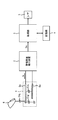
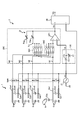
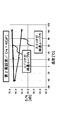
- FIG. 1 is a diagram illustrating an example of a configuration of an input device according to an embodiment of the present invention.
- the input device shown in FIG. 1 includes a sensor unit 1, a capacitance detection device 2, a processing unit 3, a storage unit 4, and an interface unit 5.
- the input device detects a capacitance between an electrode provided on the sensor unit 1 and the object when the object 6 such as a finger or a pen is close to the sensor unit 1. Based on the detection result, information corresponding to the proximity of the object 6 is input. For example, the input device acquires information such as the proximity of the object 6 to the sensor unit 1 and the distance between the sensor unit 1 and the object 6 based on the detection result of the capacitance.
- the input device is applied to a user interface device such as a touch sensor or a touch pad. Note that “proximity” in this specification means being close, and does not limit the presence or absence of contact between adjacent objects.
- the capacitance detection device 2 detects the capacitance of the capacitor Crg formed between the object 6 and the detection electrode Es, and outputs a signal Ds indicating the detection result.
- the interface unit 5 is a circuit for exchanging data between the input device and another device (for example, a host controller of an electronic device equipped with the input device).
- the processing unit 3 obtains information obtained based on the detection result of the capacitance detection device 2 (the presence / absence of the object 6, the proximity position of the object 6, the distance from the object 6, the size of the object 6, etc.) Is output to the host device (not shown) by the interface unit 5.
- a user interface that recognizes, for example, a pointing operation or a gesture operation is constructed using these pieces of information.
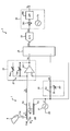
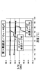
- FIG. 2 is a diagram illustrating an example of the configuration of the capacitance detection device 2 according to the first embodiment.
- the capacitance detection device 2 shown in FIG. 2 outputs a first voltage output circuit 21 that outputs a first AC voltage V1, a second voltage output circuit 22 that outputs a second AC voltage V2, and a drive current Is.
- a current output circuit 23, a subtraction circuit 24, an A / D converter 25, and a signal processing unit 26 are included.
- the capacitance ratio of the first capacitor Ca and the second capacitor Cb is adjusted so that the current I2 flowing through the capacitor Crs (shield electrode side capacitor) and the current I3 flowing through the parasitic capacitor Crgl cancel each other. That is, the capacitance ratio of the first capacitor Ca and the second capacitor Cb has a value adjusted so that the drive current Is in a state where the object 6 close to the detection electrode Es does not exist becomes zero. As shown in Expression (12) described later, when the capacitance ratio between the second capacitor Cb and the first capacitor Ca matches the capacitance ratio between the parasitic capacitor Crgl and the capacitor Crs, the current flowing through the capacitor Crs I2 and current I3 flowing through parasitic capacitor Crgl cancel each other.
- the capacitance value of the first capacitor Ca is constant, and the capacitance value of the second capacitor Cb is adjusted. That is, the second capacitor Cb has a capacitance value adjusted so that the drive current Is in a state where the object 6 close to the detection electrode Es does not exist becomes zero.
- the second capacitor Cb may be a variable-capacitance discrete component or a component formed on a semiconductor chip or the like inside the IC. In the latter case, for example, the second capacitor Cb is composed of a plurality of capacitors connected in parallel, and the capacitance value is adjusted by selecting the number of capacitors connected in parallel by laser trimming or the like.
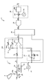
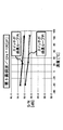
- FIG. 3 is a diagram illustrating an example of the configuration of the subtracting circuit 24.
- the subtraction circuit 24 includes a fully differential amplifier 241, resistors R1 to R7, and capacitors C1 to C3.
- the capacitor C1 is connected between the inverting input terminal and the non-inverting output terminal of the fully differential amplifier 241.
- the capacitor C2 is connected between the non-inverting input terminal and the inverting output terminal of the fully differential amplifier 241.
- the detection signal Vo is input to the inverting input terminal of the fully differential amplifier 241 via the resistors R3 and R4 connected in series.
- the detection signal Vo is input to one end of the resistor R3, and the inverting input terminal of the fully differential amplifier 241 is connected to one end of the resistor R4.
- the A / D converter 25 converts the analog differential signal Vm output from the subtraction circuit 24 into a digital signal Dm.
- a differential input type ⁇ A / D converter can be used as the A / D converter 25.
- the gain of the operational amplifier OP1 When the gain of the operational amplifier OP1 is sufficiently high, the voltage difference between the inverting input terminal and the non-inverting input terminal of the operational amplifier OP1 becomes small, and the voltage at the inverting input terminal of the operational amplifier OP1 is approximately equal to the second AC voltage V2.
- a circuit (a parallel circuit of a feedback capacitor Cag and a feedback resistor Rag in the example of FIG. 2) provided in a path between the output terminal and the inverting input terminal of the operational amplifier OP1 is referred to as a “feedback circuit Zf”. If the impedance is represented by “Zf”, the detection signal Vo is represented by the following equation.
- the detection signal Vo is expressed by the following equation.
- the reference AC voltage corresponding to the AC voltage output as the detection signal Vo from the operational amplifier OP1 in the state where the object 6 close to the detection electrode Es does not exist is generated from the detection signal Vo by the subtraction circuit 24. Subtracted.
- the signal Vm obtained as a result of this subtraction has an amplitude substantially proportional to the capacitance of the capacitor Crg, and becomes minute in a state where the object 6 close to the detection electrode Es does not exist.
- the detection signal Vo has a large amplitude corresponding to the second AC voltage V2 (Equation (9)). Therefore, by providing the subtraction circuit 24, the capacitance of the capacitor Crg can be changed.
- the dynamic range of the corresponding detection signal Vo can be further increased. Therefore, the detection sensitivity of the capacitance of the capacitor Crg can be further increased.
- the operational amplifier OP1, the first resistor Rs, and the feedback capacitor Cag of the current output circuit 23A use a low-pass filter for a signal input from the object 6 via the capacitor Crg. Constitute. Therefore, even if an AC noise voltage is superimposed between the ground where the object 6 is grounded and the ground of the capacitance detection device 2, the noise voltage is attenuated by the low-pass filter of the current output circuit 23A.
- the electrostatic capacitance detection device 2 detects the electrostatic capacitance for each of the detection electrodes Es1 to Es4.
- the capacitance detection device 2 shown in FIG. 9 has the same configuration (the first voltage output circuit 21, the second voltage output circuit 22, and the subtraction circuit 24) as the capacitance detection device 2 already described, and also has a current output.
- a circuit 23C is included.
- the operational amplifier OP1 amplifies the voltage difference between the inverting input terminal connected to any one of the detection electrodes Es1 to Es4 via the second switch circuit SW2 and the non-inverting input terminal to which the second AC voltage V2 is applied.
- the amplification result is output as a detection signal Vo.
- the feedback circuit Zf is provided in a path between the output terminal of the detection signal Vo of the operational amplifier OP1 and the common node Nc.
- the first switch circuit SW1 selects one input node from the plurality of input nodes N1 to N4 and connects it to the common node Nc.
- the fourth switch circuit SW4 selects an input node not selected by the first switch circuit SW1 and the second switch circuit SW2 from the plurality of input nodes N1 to N4, and applies the first AC voltage V1 to the selected input node. To do. That is, the fourth switch circuit SW4 applies the same first AC voltage V1 as that of the shield electrodes Ea1 to Ea4 to the detection electrode where the capacitance is not detected. As a result, current does not flow to the parasitic capacitor formed between the detection electrode where the capacitance is not detected and the detection electrode to be detected, and the influence of these parasitic capacitors is reduced. Detection sensitivity and detection accuracy are improved.
- the electrostatic capacitance detection device 2 shown in FIG. 12 when the electrostatic capacitance of the detection electrode Esi is detected (the input node Ni is selected in the first switch circuit SW1 and the second switch circuit SW2, and the third switch circuit SW3).
- the connection node NAi is selected in FIG. 7
- the configuration of the current output circuit 23D viewed from the detection electrode Esi is equivalent to the current output circuit 23B in FIG. Accordingly, the gain of the low-pass filter is increased similarly to the capacitance detection device 2 shown in FIG. 7, and the capacitance detection sensitivity is improved.
- the drive current (Is) is output from the operational amplifier (OP1) via the feedback circuit (Zf) provided in the feedback loop of the operational amplifier (OP1), and the voltage from the operational amplifier (OP1) is output.
- the detection signal (Vo) is output, the present invention is not limited to this example.
- the current output circuit may include a current output unit that outputs a current proportional to the drive current, and a current-voltage conversion unit that converts the output current into a voltage and outputs the voltage as a voltage detection signal.
Landscapes
- Engineering & Computer Science (AREA)
- General Engineering & Computer Science (AREA)
- Theoretical Computer Science (AREA)
- Physics & Mathematics (AREA)
- General Physics & Mathematics (AREA)
- Human Computer Interaction (AREA)
- Remote Sensing (AREA)
- Life Sciences & Earth Sciences (AREA)
- Electromagnetism (AREA)
- Power Engineering (AREA)
- Environmental & Geological Engineering (AREA)
- Geology (AREA)
- General Life Sciences & Earth Sciences (AREA)
- Geophysics (AREA)
- Measurement Of Resistance Or Impedance (AREA)
- Electronic Switches (AREA)
- Geophysics And Detection Of Objects (AREA)
Abstract
This capacitance detection device 2 has a first voltage output circuit 21 for outputting a first AC voltage V1 supplied to a shield electrode Ea disposed in the vicinity of a detection electrode Es, a second voltage output circuit 22 for outputting a second AC voltage V2 that has the same frequency and phase as the first AC voltage V1 and a smaller amplitude than the first AC voltage V1, and a current output circuit 23 for outputting a drive current Is to the detection electrode Es so as to reduce the voltage difference between the voltage of the detection electrode Es and the second AC voltage V2 and outputting a detection signal Vo corresponding to the drive current Is. The second voltage output circuit 22 outputs a second AC voltage V2 having an amplitude that is adjusted such that the drive current Is is zero in a state where there is no object 6 near the detection electrode Es.
Description
本発明は、対象物と電極との間の静電容量を検出する静電容量検出装置、及び、タッチパッドなどの静電容量型の入力装置に関するものである。
The present invention relates to a capacitance detection device that detects a capacitance between an object and an electrode, and a capacitance-type input device such as a touch pad.
指などの対象物の近接を静電容量に基づいて検出するタッチセンサやタッチパッドなどの入力装置が知られている。入力装置に用いられる静電容量の検出方式には、一般に、相互容量式と自己容量式がある。相互容量式では、交差して配置された2つの電極間の静電容量が検出され、自己容量式では、グランドに対する検出電極の静電容量が検出される。
Input devices such as a touch sensor and a touch pad that detect proximity of an object such as a finger based on capacitance are known. Generally, there are a mutual capacitance method and a self-capacitance method as capacitance detection methods used in the input device. In the mutual capacitance type, the capacitance between two electrodes arranged in a crossing manner is detected, and in the self capacitance type, the capacitance of the detection electrode with respect to the ground is detected.
自己容量式は、相互容量式に比べて静電容量の検出感度が高いという利点を有する。しかしながら、グランドと検出電極の間に容量の大きな寄生キャパシタが存在すると、検出結果の信号に寄生キャパシタの成分が大きな割合を占めるようになり、検出対象の容量成分のダイナミックレンジが小さくなるため、検出感度が低下する。また、寄生キャパシタの容量変動がノイズとなり、静電容量の検出精度が低下する。
The self-capacitance type has the advantage of higher electrostatic capacity detection sensitivity than the mutual capacitance type. However, if a parasitic capacitor with a large capacitance exists between the ground and the detection electrode, the parasitic capacitor component occupies a large proportion of the detection result signal, and the dynamic range of the capacitance component to be detected becomes small. Sensitivity decreases. In addition, the capacitance variation of the parasitic capacitor becomes noise, and the capacitance detection accuracy decreases.
従来、このような寄生キャパシタの影響を軽減するため、検出電極と同電位に駆動されたシールド電極(アクティブシールドとも呼ばれる)が検出電極の周囲に配置されている(例えば、下記の特許文献1を参照)。アクティブシールドを設けることにより、検出電極が周囲の導体と静電結合を生じ難くなるため、寄生キャパシタの容量が減少する。また、アクティブシールドが検出電極と同電位であるため、アクティブシールドと検出電極との間の静電容量は検出結果に影響を与えない。
Conventionally, in order to reduce the influence of such a parasitic capacitor, a shield electrode (also referred to as an active shield) driven to the same potential as the detection electrode is disposed around the detection electrode (for example, see Patent Document 1 below). reference). By providing the active shield, it becomes difficult for the detection electrode to cause electrostatic coupling with the surrounding conductor, and the capacitance of the parasitic capacitor is reduced. Further, since the active shield has the same potential as the detection electrode, the capacitance between the active shield and the detection electrode does not affect the detection result.
アクティブシールドによって寄生キャパシタの容量は減少するものの、全てを無くすことはできない。そのため、より高い検出感度を得ようとした場合は、残留する寄生キャパシタの影響が問題となる。
ア ク テ ィ ブ Although the capacitance of the parasitic capacitor is reduced by the active shield, it cannot be completely eliminated. Therefore, when trying to obtain higher detection sensitivity, the effect of the remaining parasitic capacitor becomes a problem.
上記の特許文献2に記載される装置では、被測定容量に応じた電流が検出回路において電圧に変換され、この検出回路の出力電圧が補正回路に入力されて、寄生キャパシタの影響による位相のずれが補正される(特許文献2の図1等)。しかしながら、検出回路の出力電圧の振幅が寄生キャパシタの影響によって増大するため、被測定容量のダイナミックレンジが小さくなり、検出感度が低下するという問題がある。
In the device described in Patent Document 2 above, a current corresponding to the capacitance to be measured is converted into a voltage in the detection circuit, and the output voltage of this detection circuit is input to the correction circuit to cause a phase shift due to the influence of the parasitic capacitor. Is corrected (FIG. 1, etc. of Patent Document 2). However, since the amplitude of the output voltage of the detection circuit increases due to the influence of the parasitic capacitor, there is a problem that the dynamic range of the capacitance to be measured is reduced and the detection sensitivity is lowered.
他方、特許文献3に記載される装置では、検出対象のキャパシタに流れる駆動電流に比例した検出電流が電流出力回路から出力され、この検出電流に補正用キャパシタを介して補正電流が加えられることで、寄生キャパシタによる電流の増大分が相殺される(特許文献3の図7等)。しかしながら、補正用キャパシタの静電容量は寄生キャパシタに相当する微小な値に設定する必要があるため、静電容量の設定精度を高め難いという問題がある。
On the other hand, in the device described in Patent Document 3, a detection current proportional to the drive current flowing through the capacitor to be detected is output from the current output circuit, and the correction current is added to the detection current via the correction capacitor. Thus, the increase in current due to the parasitic capacitor is canceled (FIG. 7 in Patent Document 3). However, since the capacitance of the correction capacitor needs to be set to a minute value corresponding to the parasitic capacitor, there is a problem that it is difficult to increase the capacitance setting accuracy.
本発明はかかる事情に鑑みてなされたものであり、その目的は、寄生キャパシタの影響による検出感度や検出精度の低下を抑制できる静電容量検出装置と、これを備えた入力装置を提供することにある。
The present invention has been made in view of such circumstances, and an object thereof is to provide a capacitance detection device capable of suppressing a decrease in detection sensitivity and detection accuracy due to the influence of a parasitic capacitor, and an input device including the same. It is in.
本発明の第1の観点は、検出電極に近接する対象物と前記検出電極との間の静電容量を検出する静電容量検出装置に関する。この静電容量検出装置は、前記検出電極に近接して配置されたシールド電極に供給される第1交流電圧を出力する第1電圧出力回路と、周波数と位相が前記第1交流電圧に等しく、かつ、振幅が前記第1交流電圧より小さい第2交流電圧を出力する第2電圧出力回路と、前記検出電極の電圧と前記第2交流電圧との電圧差が小さくなるように前記検出電極へ駆動電流を出力するとともに、当該駆動電流に応じた検出信号を出力する電流出力回路とを有する。前記第2電圧出力回路は、前記検出電極に近接する前記対象物が存在しない状態における前記駆動電流がゼロになるように振幅が調整された前記第2交流電圧を出力する。
A first aspect of the present invention relates to a capacitance detection device that detects a capacitance between an object close to a detection electrode and the detection electrode. The capacitance detection device includes a first voltage output circuit that outputs a first AC voltage supplied to a shield electrode disposed in proximity to the detection electrode, a frequency and a phase equal to the first AC voltage, In addition, a second voltage output circuit that outputs a second AC voltage having an amplitude smaller than the first AC voltage, and driving the detection electrode so that a voltage difference between the voltage of the detection electrode and the second AC voltage is small. A current output circuit for outputting a current and outputting a detection signal corresponding to the drive current. The second voltage output circuit outputs the second AC voltage whose amplitude is adjusted so that the drive current becomes zero in a state where the object close to the detection electrode does not exist.
この構成によれば、前記検出電極と前記シールド電極との間に形成されるキャパシタ(以下、「シールド電極側キャパシタ」と記す場合がある。)には、前記第1交流電圧と前記第2交流電圧との差に応じた交流電流が流れる。前記第2交流電圧の振幅が、前記検出電極に近接する前記対象物が存在しない状態における前記駆動電流がゼロになるように調整された振幅であるため、シールド電極側キャパシタに流れる交流電流は、前記検出電極の寄生キャパシタ(以下、単に「寄生キャパシタ」と記す場合がある。)に流れる交流電流と概ね等しくなる。すなわち、シールド電極側キャパシタに流れる交流電流と寄生キャパシタに流れる交流電流とが相殺されることにより、前記駆動電流には、寄生キャパシタによる交流電流が殆ど含まれなくなる。そのため、前記電流出力回路から出力される前記検出信号は、寄生キャパシタによる成分を殆ど含まなくなる。従って、前記対象物と前記検出電極との間の静電容量(以下、「被検出容量」と記す場合がある。)の検出感度や検出精度が、寄生キャパシタの影響を受け難くなる。
According to this configuration, the capacitor formed between the detection electrode and the shield electrode (hereinafter sometimes referred to as “shield electrode side capacitor”) has the first AC voltage and the second AC. An alternating current flows according to the difference from the voltage. Since the amplitude of the second AC voltage is an amplitude adjusted so that the drive current in a state where the object adjacent to the detection electrode does not exist, the AC current flowing through the shield electrode side capacitor is This is approximately equal to the alternating current flowing in the parasitic capacitor of the detection electrode (hereinafter sometimes simply referred to as “parasitic capacitor”). That is, the alternating current flowing through the shield electrode capacitor and the alternating current flowing through the parasitic capacitor cancel each other, so that the drive current hardly includes the alternating current due to the parasitic capacitor. Therefore, the detection signal output from the current output circuit hardly includes a component due to a parasitic capacitor. Therefore, the detection sensitivity and detection accuracy of the capacitance between the object and the detection electrode (hereinafter sometimes referred to as “detected capacitance”) are not easily affected by the parasitic capacitor.
好適に、前記第2電圧出力回路は、前記第1交流電圧を減衰させた電圧を前記第2交流電圧として出力する。
Preferably, the second voltage output circuit outputs a voltage obtained by attenuating the first AC voltage as the second AC voltage.
この構成によれば、減衰器を用いて前記第1交流電圧から前記第2交流電圧を生成することが可能になる。トランジスタ等の能動素子を含まない減衰器を用いることにより、前記第2交流電圧のノイズが小さくなり、被検出容量の検出精度が向上する。
According to this configuration, the second AC voltage can be generated from the first AC voltage using an attenuator. By using an attenuator that does not include an active element such as a transistor, the noise of the second AC voltage is reduced, and the detection accuracy of the detected capacitance is improved.
好適に、前記第2電圧出力回路は、第1キャパシタと第2キャパシタとの直列回路を含んでよい。前記第1電圧出力回路は、前記直列回路の両端に前記第1交流電圧を印加してよい。前記第2キャパシタにおいて、前記第1交流電圧に応じた前記第2交流電圧が生じてよい。
Preferably, the second voltage output circuit may include a series circuit of a first capacitor and a second capacitor. The first voltage output circuit may apply the first AC voltage to both ends of the series circuit. In the second capacitor, the second AC voltage corresponding to the first AC voltage may be generated.
この構成によれば、前記第1キャパシタと前記第2キャパシタとの直列回路に前記第1交流電圧が印加され、前記第1交流電圧に応じた前記第2交流電圧が前記第2キャパシタにおいて生じる。そのため、抵抗による減衰器を用いる場合に比べてノイズが小さくなる。
According to this configuration, the first AC voltage is applied to a series circuit of the first capacitor and the second capacitor, and the second AC voltage corresponding to the first AC voltage is generated in the second capacitor. For this reason, noise is reduced as compared with the case where an attenuator using resistors is used.
好適に、前記第1キャパシタと前記第2キャパシタとの静電容量比が、前記検出電極に近接する前記対象物が存在しない状態における前記駆動電流がゼロになるように調整された値を持ってよい。
Preferably, a capacitance ratio between the first capacitor and the second capacitor has a value adjusted so that the driving current is zero in a state where the object adjacent to the detection electrode is not present. Good.
この構成によれば、前記第1キャパシタと前記第2キャパシタとの静電容量比の調整により、前記第2交流電圧の振幅が調整され、この振幅の調整により、シールド電極側キャパシタに流れる交流電流と寄生キャパシタに流れる交流電流とが相殺される。そのため、前記第1キャパシタ及び前記第2キャパシタの静電容量は、寄生キャパシタの静電容量に依らず、比較的大きな値にすることが可能となる。前記第1キャパシタ及び前記第2キャパシタの静電容量が大きくなることで、前記静電容量比の設定精度を高めやすくなり、前記シールド電極側キャパシタに流れる交流電流と寄生キャパシタに流れる交流電流とを精度よく相殺することが可能になる。
According to this configuration, the amplitude of the second AC voltage is adjusted by adjusting the capacitance ratio between the first capacitor and the second capacitor, and the AC current flowing through the shield electrode side capacitor is adjusted by adjusting the amplitude. And the alternating current flowing through the parasitic capacitor cancel each other. Therefore, the capacitances of the first capacitor and the second capacitor can be set to a relatively large value regardless of the capacitance of the parasitic capacitor. By increasing the capacitance of the first capacitor and the second capacitor, it becomes easier to increase the setting accuracy of the capacitance ratio, and the alternating current flowing through the shield electrode side capacitor and the alternating current flowing through the parasitic capacitor are reduced. It becomes possible to cancel with high accuracy.
好適に、前記第2キャパシタの静電容量値が調整可能であって、前記第2キャパシタは、前記検出電極に近接する前記対象物が存在しない状態における前記駆動電流がゼロになるように調整された静電容量値を持ってよい。
Preferably, the capacitance value of the second capacitor can be adjusted, and the second capacitor is adjusted so that the drive current becomes zero in a state where the object adjacent to the detection electrode does not exist. You may have a capacitance value.
この構成によれば、前記第2キャパシタの静電容量値の調整により、前記第2交流電圧の振幅が調整され、この振幅の調整により、前記シールド電極側キャパシタに流れる交流電流と寄生キャパシタに流れる交流電流とが相殺される。この交流電流の相殺が成立する場合、前記第2キャパシタの静電容量と寄生キャパシタの静電容量とが比例するため、前記第2キャパシタの静電容量の調整が容易になる。
According to this configuration, the amplitude of the second AC voltage is adjusted by adjusting the capacitance value of the second capacitor, and the AC current flowing in the shield electrode side capacitor and the parasitic capacitor flows by adjusting the amplitude. AC current is offset. When this AC current cancellation is established, the capacitance of the second capacitor is proportional to the capacitance of the parasitic capacitor, so that the capacitance of the second capacitor can be easily adjusted.
好適に、前記電流出力回路は、前記検出電極に接続される反転入力端子と前記第2交流電圧が印加される非反転入力端子との電圧差を増幅し、当該増幅結果を前記検出信号として出力する演算増幅器と、前記演算増幅器の前記検出信号の出力端子と前記反転入力端子との間の経路に設けられた帰還キャパシタと、前記帰還キャパシタと並列に接続された帰還抵抗と、前記演算増幅器の前記反転入力端子と前記検出電極との間の経路に設けられた第1抵抗とを含んでよい。
Preferably, the current output circuit amplifies a voltage difference between an inverting input terminal connected to the detection electrode and a non-inverting input terminal to which the second AC voltage is applied, and outputs the amplification result as the detection signal. An operational amplifier, a feedback capacitor provided in a path between the output terminal of the detection signal and the inverting input terminal of the operational amplifier, a feedback resistor connected in parallel with the feedback capacitor, and the operational amplifier A first resistor provided in a path between the inverting input terminal and the detection electrode may be included.
この構成によれば、前記帰還キャパシタと前記第1抵抗と前記演算増幅器とによりローパスフィルタが構成されるため、前記検出電極を介して入力されるノイズが減衰し、検出精度の低下が抑えられる。
According to this configuration, since the low-pass filter is configured by the feedback capacitor, the first resistor, and the operational amplifier, noise input through the detection electrode is attenuated, and a decrease in detection accuracy is suppressed.
好適に、前記電流出力回路は、前記検出電極に接続される反転入力端子と前記第2交流電圧が印加される非反転入力端子との電圧差を増幅し、当該増幅結果を前記検出信号として出力する演算増幅器と、前記演算増幅器の前記検出信号の出力端子と前記反転入力端子との間の経路に設けられた帰還キャパシタと、前記演算増幅器の前記反転入力端子と前記検出電極との間の経路に設けられた第1抵抗と、前記検出電極に接続される前記第1抵抗の一端と前記演算増幅器の前記出力端子との間の経路に設けられた帰還抵抗とを含んでよい。
Preferably, the current output circuit amplifies a voltage difference between an inverting input terminal connected to the detection electrode and a non-inverting input terminal to which the second AC voltage is applied, and outputs the amplification result as the detection signal. An operational amplifier, a feedback capacitor provided in a path between the output terminal of the detection signal and the inverting input terminal of the operational amplifier, and a path between the inverting input terminal of the operational amplifier and the detection electrode And a feedback resistor provided in a path between one end of the first resistor connected to the detection electrode and the output terminal of the operational amplifier.
この構成によれば、前記帰還キャパシタと前記第1抵抗と前記帰還抵抗と前記演算増幅器とによりローパスフィルタが構成されるため、前記検出電極を介して入力されるノイズが減衰し、検出精度が向上する。また、前記ローパスフィルタのゲインの伝達関数における極が複素極となり、極付近の周波数においてゲインが高くなるため、検出感度が高くなる。
According to this configuration, since the feedback capacitor, the first resistor, the feedback resistor, and the operational amplifier constitute a low-pass filter, noise input through the detection electrode is attenuated and detection accuracy is improved. To do. Further, the pole in the gain transfer function of the low-pass filter becomes a complex pole, and the gain becomes high at frequencies near the pole, so that the detection sensitivity becomes high.
好適に、前記第1電圧出力回路及び前記第2電圧出力回路は、出力する交流電圧の周波数をそれぞれ変更可能であってよい。前記第1抵抗は、前記第1交流電圧及び前記第2交流電圧の周波数に応じて抵抗値が変更される可変抵抗であってよい。
Preferably, the first voltage output circuit and the second voltage output circuit may each be capable of changing the frequency of the alternating voltage to be output. The first resistor may be a variable resistor whose resistance value is changed according to the frequency of the first AC voltage and the second AC voltage.
この構成によれば、前記第1交流電圧及び前記第2交流電圧の周波数(以下、「駆動周波数」と記す場合がある。)をそれぞれ変更可能であるため、ノイズの影響が小さくなるように周波数を選択することが可能になる。また、前記第1交流電圧及び前記第2交流電圧の周波数に応じて、前記ローパスフィルタのカットオフ周波数を適切に設定することが可能になる。
According to this configuration, since the frequencies of the first AC voltage and the second AC voltage (hereinafter sometimes referred to as “drive frequency”) can be changed, the frequency is reduced so that the influence of noise is reduced. It becomes possible to select. Further, it becomes possible to appropriately set the cut-off frequency of the low-pass filter in accordance with the frequencies of the first AC voltage and the second AC voltage.
好適に、前記帰還キャパシタの静電容量値及び前記帰還抵抗の抵抗値がそれぞれ調整可能であってよい。
Preferably, the capacitance value of the feedback capacitor and the resistance value of the feedback resistor may be adjustable.
この構成によれば、前記帰還キャパシタの静電容量値及び前記帰還抵抗の抵抗値がそれぞれ調整可能であるため、前記第1交流電圧及び前記第2交流電圧と前記検出信号との位相差や、被測定容量に対する検出信号のゲインを適切に調整することが可能になる。
According to this configuration, since the capacitance value of the feedback capacitor and the resistance value of the feedback resistor can be adjusted, respectively, the phase difference between the first AC voltage and the second AC voltage and the detection signal, It is possible to appropriately adjust the gain of the detection signal with respect to the measured capacitance.
好適に、前記電流出力回路は、前記検出電極に接続される反転入力端子と前記第2交流電圧が印加される非反転入力端子との電圧差を増幅し、当該増幅結果を前記検出信号として出力する演算増幅器と、前記演算増幅器の前記検出信号の出力端子と前記反転入力端子との間の経路に設けられた帰還回路とを含んでよい。また、上記静電容量検出装置は、前記検出電極に近接する前記対象物が存在しない状態において前記演算増幅器から前記検出信号として出力される交流電圧に相当する基準交流電圧を前記検出信号から減算する減算回路を有してよい。
Preferably, the current output circuit amplifies a voltage difference between an inverting input terminal connected to the detection electrode and a non-inverting input terminal to which the second AC voltage is applied, and outputs the amplification result as the detection signal. And a feedback circuit provided in a path between the output terminal of the detection signal and the inverting input terminal of the operational amplifier. The capacitance detection device subtracts a reference AC voltage corresponding to an AC voltage output as the detection signal from the operational amplifier from the detection signal in a state where the object close to the detection electrode does not exist. A subtraction circuit may be included.
この構成によれば、前記検出電極に近接する前記対象物が存在しない状態において前記演算増幅器から前記検出信号として出力される交流電圧に相当する前記基準交流電圧が、前記検出信号から減算される。この減算の結果として得られる信号は、前記検出信号の被検出容量にほぼ比例した振幅を持ち、前記検出電極に近接する前記対象物が存在しない状態において微小になる。そのため、被検出容量の変化に対応する前記検出信号のダイナミックレンジがより大きくなり、被検出容量の検出感度が向上する。
According to this configuration, the reference AC voltage corresponding to the AC voltage output as the detection signal from the operational amplifier in a state where the object adjacent to the detection electrode does not exist is subtracted from the detection signal. The signal obtained as a result of this subtraction has an amplitude substantially proportional to the detected capacitance of the detection signal, and becomes minute in a state where the object close to the detection electrode does not exist. Therefore, the dynamic range of the detection signal corresponding to the change in the detected capacitance is further increased, and the detection sensitivity of the detected capacitance is improved.
好適に、前記減算回路は、前記検出信号と前記第1交流電圧とを入力し、前記第1交流電圧を減衰させた電圧である前記基準交流電圧を前記検出信号から減算してよい。
Preferably, the subtraction circuit may receive the detection signal and the first AC voltage, and subtract the reference AC voltage, which is a voltage obtained by attenuating the first AC voltage, from the detection signal.
この構成によれば、前記減算回路において前記検出信号から減算される前記基準交流電圧が、前記第1交流電圧を減衰させた電圧であるため、前記検出信号に含まれるノイズ成分と前記基準交流電圧に含まれるノイズ成分との相関性が高い。これにより、前記減算回路の減算結果として得られる信号のノイズ成分が減少する。
According to this configuration, since the reference AC voltage subtracted from the detection signal in the subtraction circuit is a voltage obtained by attenuating the first AC voltage, the noise component included in the detection signal and the reference AC voltage Correlation with the noise component contained in is high. Thereby, the noise component of the signal obtained as a subtraction result of the subtraction circuit is reduced.
好適に、前記減算回路は、前記検出信号から前記基準交流電圧を減算した結果を差動信号として出力してよい。
Preferably, the subtraction circuit may output a result obtained by subtracting the reference AC voltage from the detection signal as a differential signal.
この構成によれば、全差動アンプを用いて前記減算回路を構成することが可能である。
According to this configuration, the subtraction circuit can be configured using a fully differential amplifier.
好適に、前記電流出力回路は、前記検出電極に接続される反転入力端子と前記第2交流電圧が印加される非反転入力端子との電圧差を増幅し、当該増幅結果を前記検出信号として出力する演算増幅器と、前記演算増幅器の前記検出信号の出力端子と共通ノードとの間の経路に設けられた帰還回路と、複数の入力ノードから1つの前記入力ノードを選択して前記共通ノードに接続する第1スイッチ回路と、前記複数の入力ノードから前記第1スイッチ回路と同じ1つの前記入力ノードを選択して前記反転入力端子に接続する第2スイッチ回路とを含んでよい。前記複数の入力ノードが、それぞれ異なる前記検出電極に接続されてよい。
Preferably, the current output circuit amplifies a voltage difference between an inverting input terminal connected to the detection electrode and a non-inverting input terminal to which the second AC voltage is applied, and outputs the amplification result as the detection signal. An operational amplifier, a feedback circuit provided in a path between the output terminal of the detection signal of the operational amplifier and a common node, and one input node selected from a plurality of input nodes and connected to the common node And a second switch circuit that selects the same input node as the first switch circuit from the plurality of input nodes and connects the selected input node to the inverting input terminal. The plurality of input nodes may be connected to the different detection electrodes.
この構成によれば、前記演算増幅器の前記反転入力端子と前記出力端子との間の帰還ループに前記第1スイッチ回路及び前記第2スイッチ回路の各スイッチが挿入される。 MOSトランジスタ等によるスイッチは、信号レベルに応じて導通抵抗が変化する非線形性を有する。駆動周波数における前記帰還回路のインピーダンスが、前記検出電極側のインピーダンス(主にシールド電極側キャパシタのインピーダンス)に比べて大きいものとすると、前記第1スイッチ回路のスイッチを前記入力ノードと前記共通ノードとの間の経路に設けることにより、前記入力ノードと前記検出電極との間の経路にスイッチを設ける場合に比べて、前記非線形性による影響(前記検出信号の歪など)が抑制される。また、前記演算増幅器の前記反転入力端子のインピーダンスは非常に大きいため、前記入力ノードと前記反転入力端子との間に前記第2スイッチ回路のスイッチを設けることにより、前記非線形性の影響がほとんど生じない。
According to this configuration, each switch of the first switch circuit and the second switch circuit is inserted into a feedback loop between the inverting input terminal and the output terminal of the operational amplifier. A switch such as a MOS transistor has non-linearity in which the conduction resistance changes according to the signal level. When the impedance of the feedback circuit at the driving frequency is larger than the impedance on the detection electrode side (mainly the impedance of the shield electrode side capacitor), the switch of the first switch circuit is connected to the input node and the common node. By providing in the path between, the influence by the non-linearity (such as distortion of the detection signal) is suppressed as compared with the case where a switch is provided in the path between the input node and the detection electrode. Further, since the impedance of the inverting input terminal of the operational amplifier is very large, the influence of the non-linearity is almost caused by providing a switch of the second switch circuit between the input node and the inverting input terminal. Absent.
好適に、前記電流出力回路は、前記複数の入力ノードと前記複数の検出電極との間の複数の経路に設けられた複数の第1抵抗を含んでよい。前記帰還回路は、並列に接続された帰還キャパシタと帰還抵抗とを含んでよい。
Preferably, the current output circuit may include a plurality of first resistors provided in a plurality of paths between the plurality of input nodes and the plurality of detection electrodes. The feedback circuit may include a feedback capacitor and a feedback resistor connected in parallel.
この構成によれば、前記帰還キャパシタと前記第1抵抗と前記演算増幅器とによりローパスフィルタが構成されるため、前記検出電極を介して入力されるノイズが減衰し、検出精度の低下が抑制される。
According to this configuration, since the low-pass filter is configured by the feedback capacitor, the first resistor, and the operational amplifier, noise input through the detection electrode is attenuated, and a decrease in detection accuracy is suppressed. .
好適に、前記電流出力回路は、前記複数の入力ノードと前記複数の検出電極との間の複数の経路に設けられた複数の第1抵抗と、前記複数の検出電極と前記複数の第1抵抗とを接続する複数の接続ノードから1つの接続ノードを選択して前記演算増幅器の前記出力端子に接続する第3スイッチ回路と、前記第3スイッチ回路と前記出力端子との間の経路に設けられた帰還抵抗とを含んでよい。前記帰還回路は、帰還キャパシタを含んでよい。
Preferably, the current output circuit includes a plurality of first resistors provided in a plurality of paths between the plurality of input nodes and the plurality of detection electrodes, the plurality of detection electrodes, and the plurality of first resistors. And a third switch circuit for selecting one connection node from a plurality of connection nodes for connecting to the output terminal of the operational amplifier and a path between the third switch circuit and the output terminal. Feedback resistors. The feedback circuit may include a feedback capacitor.
この構成によれば、前記帰還キャパシタと前記第1抵抗と前記帰還抵抗と前記演算増幅器とによりローパスフィルタが構成されるため、前記検出電極を介して入力されるノイズが減衰し、検出精度の低下が抑制される。また、前記ローパスフィルタのゲインの伝達関数における極が複素極となり、極付近の周波数においてゲインが高くなるため、検出感度が高くなる。
According to this configuration, since the low-pass filter is configured by the feedback capacitor, the first resistor, the feedback resistor, and the operational amplifier, noise input through the detection electrode is attenuated, and detection accuracy is reduced. Is suppressed. Further, the pole in the gain transfer function of the low-pass filter becomes a complex pole, and the gain becomes high at frequencies near the pole, so that the detection sensitivity becomes high.
本発明の第2の観点は、対象物の近接に応じた情報を入力する入力装置に関する。この入力装置は、前記対象物の近接に応じて前記対象物との間の静電容量が変化する少なくとも1つの検出電極と、前記検出電極に近接して配置されたシールド電極と、前記対象物と前記検出電極との間の静電容量を検出する上記第1の観点の静電容量検出装置とを有する。
The second aspect of the present invention relates to an input device that inputs information according to the proximity of an object. The input device includes at least one detection electrode whose capacitance changes with the object in accordance with the proximity of the object, a shield electrode arranged in proximity to the detection electrode, and the object And the capacitance detection device according to the first aspect for detecting the capacitance between the detection electrode and the detection electrode.
本発明によれば、寄生キャパシタの影響による検出感度や検出精度の低下を抑制できる静電容量検出装置と、これを備えた入力装置を提供できる。
According to the present invention, it is possible to provide a capacitance detection device that can suppress a decrease in detection sensitivity and detection accuracy due to the influence of a parasitic capacitor, and an input device including the same.
<第1の実施形態>
図1は、本発明の実施形態に係る入力装置の構成の一例を示す図である。図1に示す入力装置は、センサ部1と、静電容量検出装置2と、処理部3と、記憶部4と、インターフェース部5を有する。 <First Embodiment>
FIG. 1 is a diagram illustrating an example of a configuration of an input device according to an embodiment of the present invention. The input device shown in FIG. 1 includes asensor unit 1, a capacitance detection device 2, a processing unit 3, a storage unit 4, and an interface unit 5.
図1は、本発明の実施形態に係る入力装置の構成の一例を示す図である。図1に示す入力装置は、センサ部1と、静電容量検出装置2と、処理部3と、記憶部4と、インターフェース部5を有する。 <First Embodiment>
FIG. 1 is a diagram illustrating an example of a configuration of an input device according to an embodiment of the present invention. The input device shown in FIG. 1 includes a
本実施形態に係る入力装置は、指やペンなどの対象物6がセンサ部1に近接した場合に、センサ部1に設けられた電極と対象物との間の静電容量を検出し、この検出結果に基づいて、対象物6の近接に応じた情報を入力する。例えば入力装置は、センサ部1に対する対象物6の近接の有無や、センサ部1と対象物6との距離などの情報を、静電容量の検出結果に基づいて取得する。入力装置は、例えばタッチセンサやタッチパッドなどのユーザーインターフェース装置に適用される。なお、本明細書における「近接」とは、近くにあることを意味しており、近接する物同士の接触の有無を限定しない。
The input device according to the present embodiment detects a capacitance between an electrode provided on the sensor unit 1 and the object when the object 6 such as a finger or a pen is close to the sensor unit 1. Based on the detection result, information corresponding to the proximity of the object 6 is input. For example, the input device acquires information such as the proximity of the object 6 to the sensor unit 1 and the distance between the sensor unit 1 and the object 6 based on the detection result of the capacitance. The input device is applied to a user interface device such as a touch sensor or a touch pad. Note that “proximity” in this specification means being close, and does not limit the presence or absence of contact between adjacent objects.
センサ部1は、指やペンなどの対象物6の近接を検出するための検出電極Esと、検出電極Esに近接して配置されたシールド電極Eaを有する。検出電極Esは、センサ部1において対象物が近接する領域に配置される。例えば、対象物6の検出領域の表面が絶縁性のカバー層で覆われており、カバー層より下層側に検出電極Esが配置される。シールド電極Eaは、対象物6以外の導体と検出電極Esとの静電結合を防止するための静電シールドであり、対象物6の検出領域において検出電極Esよりも下層側に配置される。
The sensor unit 1 includes a detection electrode Es for detecting the proximity of an object 6 such as a finger or a pen, and a shield electrode Ea disposed in proximity to the detection electrode Es. The detection electrode Es is arranged in a region where the object is close in the sensor unit 1. For example, the surface of the detection region of the object 6 is covered with an insulating cover layer, and the detection electrode Es is disposed on the lower layer side of the cover layer. The shield electrode Ea is an electrostatic shield for preventing electrostatic coupling between a conductor other than the object 6 and the detection electrode Es, and is disposed on a lower layer side than the detection electrode Es in the detection region of the object 6.
図1に示すように、検出電極Esと対象物6との間には、静電容量の検出対象であるキャパシタCrgが形成される。シールド電極Eaと検出電極Esとの間には、キャパシタCrs(シールド電極側キャパシタ)が形成される。また、検出電極Esとグランドとの間には、寄生キャパシタCrglが形成される。
As shown in FIG. 1, a capacitor Crg that is a capacitance detection target is formed between the detection electrode Es and the target object 6. A capacitor Crs (shield electrode side capacitor) is formed between the shield electrode Ea and the detection electrode Es. A parasitic capacitor Crgl is formed between the detection electrode Es and the ground.
静電容量検出装置2は、対象物6と検出電極Esとの間に形成されるキャパシタCrgの静電容量を検出し、その検出結果を示す信号Dsを出力する。
The capacitance detection device 2 detects the capacitance of the capacitor Crg formed between the object 6 and the detection electrode Es, and outputs a signal Ds indicating the detection result.
処理部3は、入力装置の全体的な動作を制御する回路であり、例えば、記憶部4に格納されるプログラムの命令コードに従って処理を実行するコンピュータや、特定の機能を実現するロジック回路を含む。処理部3の処理は、コンピュータにおいてプログラムに基づいて実現してもよいし、少なくとも一部を専用のロジック回路で実現してもよい。
The processing unit 3 is a circuit that controls the overall operation of the input device, and includes, for example, a computer that executes processing according to an instruction code of a program stored in the storage unit 4 and a logic circuit that realizes a specific function. . The processing of the processing unit 3 may be realized based on a program in a computer, or at least a part thereof may be realized by a dedicated logic circuit.
処理部3は、静電容量検出装置2にから出力される検出結果の信号Dsに基づいて、対象物6がセンサ部1に近接しているか否かの判定や、対象物6とセンサ部1との距離の算出を行う。なお、後述する図9等の実施形態のように、センサ部1は複数の検出電極Esを含んでいてもよく、静電容量検出装置2は複数の検出電極Esの各々についてキャパシタCrgの静電容量の検出を行ってもよい。この場合、処理部3は、各検出電極Esについて得られた検出結果の信号Dsに基づいて、センサ部1における対象物6の近接位置や、対象物6の大きさなどを算出してもよい。
The processing unit 3 determines whether or not the object 6 is close to the sensor unit 1 based on the detection result signal Ds output from the capacitance detection device 2, and determines whether the object 6 and the sensor unit 1 are in close proximity. And the distance is calculated. Note that the sensor unit 1 may include a plurality of detection electrodes Es as in the embodiment of FIG. 9 and the like which will be described later, and the electrostatic capacitance detection device 2 uses the electrostatic capacity of the capacitor Crg for each of the plurality of detection electrodes Es. Capacitance detection may be performed. In this case, the processing unit 3 may calculate the proximity position of the object 6 in the sensor unit 1 and the size of the object 6 based on the detection result signal Ds obtained for each detection electrode Es. .
また、処理部3は、外来ノイズの影響による静電容量検出装置2の検出感度の低下を回避するため、後述する静電容量検出装置2の第1交流電圧V1の周波数を変更する処理も行う。
The processing unit 3 also performs a process of changing the frequency of the first AC voltage V1 of the capacitance detection device 2 to be described later in order to avoid a decrease in detection sensitivity of the capacitance detection device 2 due to the influence of external noise. .
記憶部4は、処理部3を構成するコンピュータのプログラムや、処理部3において処理に使用されるデータ、処理の過程で一時的に保持されるデータなどを記憶する。記憶部4は、例えばDRAMやSRAM、フラッシュメモリ、ハードディスクなど、任意の記憶デバイスを用いて構成される。
The storage unit 4 stores a computer program constituting the processing unit 3, data used for processing in the processing unit 3, data temporarily stored in the course of processing, and the like. The storage unit 4 is configured using an arbitrary storage device such as a DRAM, SRAM, flash memory, or hard disk.
インターフェース部5は、入力装置と他の装置(例えば入力装置を搭載する電子機器のホストコントローラなど)との間でデータをやり取りするための回路である。処理部3は、静電容量検出装置2の検出結果に基づいて得られた情報(対象物6の有無、対象物6の近接位置、対象物6との距離、対象物6の大きさなど)を、インターフェース部5によって図示しない上位装置に出力する。上位装置では、これらの情報を用いて、例えばポインティング操作やジェスチャ操作などを認識するユーザーインターフェースが構築される。
The interface unit 5 is a circuit for exchanging data between the input device and another device (for example, a host controller of an electronic device equipped with the input device). The processing unit 3 obtains information obtained based on the detection result of the capacitance detection device 2 (the presence / absence of the object 6, the proximity position of the object 6, the distance from the object 6, the size of the object 6, etc.) Is output to the host device (not shown) by the interface unit 5. In the host device, a user interface that recognizes, for example, a pointing operation or a gesture operation is constructed using these pieces of information.
次に、静電容量検出装置2の構成について説明する。図2は、第1の実施形態に係る静電容量検出装置2の構成の一例を示す図である。図2に示す静電容量検出装置2は、第1交流電圧V1を出力する第1電圧出力回路21と、第2交流電圧V2を出力する第2電圧出力回路22と、駆動電流Isを出力する電流出力回路23と、減算回路24と、A/D変換器25と、信号処理部26を有する。
Next, the configuration of the capacitance detection device 2 will be described. FIG. 2 is a diagram illustrating an example of the configuration of the capacitance detection device 2 according to the first embodiment. The capacitance detection device 2 shown in FIG. 2 outputs a first voltage output circuit 21 that outputs a first AC voltage V1, a second voltage output circuit 22 that outputs a second AC voltage V2, and a drive current Is. A current output circuit 23, a subtraction circuit 24, an A / D converter 25, and a signal processing unit 26 are included.
第1電圧出力回路21は、シールド電極Eaに供給される第1交流電圧V1を出力する。例えば第1電圧出力回路21は、一定の振幅及び周波数を持つ正弦波の第1交流電圧V1を発生する。
The first voltage output circuit 21 outputs the first AC voltage V1 supplied to the shield electrode Ea. For example, the first voltage output circuit 21 generates a sine wave first AC voltage V1 having a constant amplitude and frequency.
また、第1電圧出力回路21は、処理部3の制御に従って第1交流電圧V1の周波数を変更することが可能である。外来ノイズの周波数と第1交流電圧V1の周波数とが近いことによる検出感度の低下を回避するため、処理部3は第1交流電圧V1の周波数を変更する制御を行う。
Further, the first voltage output circuit 21 can change the frequency of the first AC voltage V <b> 1 according to the control of the processing unit 3. In order to avoid a decrease in detection sensitivity due to the closeness of the frequency of the external noise and the frequency of the first AC voltage V1, the processing unit 3 performs control to change the frequency of the first AC voltage V1.
第2電圧出力回路22は、周波数と位相が第1交流電圧V1に等しく、かつ、振幅が第1交流電圧V1より小さい第2交流電圧V2を出力する。第2交流電圧V2の振幅は、キャパシタCrs(シールド電極側キャパシタ)に流れる電流I2と寄生キャパシタCrglに流れる電流I3とが相殺されるように調整される。すなわち、第2電圧出力回路22は、検出電極Esに近接する対象物6が存在しない状態(キャパシタCrgの静電容量がゼロの状態)における電流出力回路23の駆動電流Isがゼロになるように振幅が調整された第2交流電圧V2を出力する。
The second voltage output circuit 22 outputs a second AC voltage V2 whose frequency and phase are equal to the first AC voltage V1 and whose amplitude is smaller than the first AC voltage V1. The amplitude of the second AC voltage V2 is adjusted such that the current I2 flowing through the capacitor Crs (shield electrode side capacitor) and the current I3 flowing through the parasitic capacitor Crgl cancel each other. That is, the second voltage output circuit 22 is configured so that the drive current Is of the current output circuit 23 becomes zero in a state where the object 6 adjacent to the detection electrode Es does not exist (capacitance of the capacitor Crg is zero). The second AC voltage V2 whose amplitude is adjusted is output.
第2電圧出力回路22は、例えば減衰器であり、第1交流電圧V1を減衰させた電圧を第2交流電圧V2として出力する。図2の例において、第2電圧出力回路22は、第1キャパシタCa及び第2キャパシタCbの直列回路を含む。第1電圧出力回路21は、この直列回路の両端に第1交流電圧V1を印加する。第1交流電圧V1が第1キャパシタCa及び第2キャパシタCbにより分圧されることで、第2キャパシタCbに第2交流電圧V2が生じる。第1キャパシタCaの一方の端子が第1電圧出力回路21の出力に接続され、第1キャパシタCaの他方の端子が第2キャパシタCbの一方の端子に接続され、第2キャパシタCbの他方の端子がグランドに接続される。
The second voltage output circuit 22 is an attenuator, for example, and outputs a voltage obtained by attenuating the first AC voltage V1 as the second AC voltage V2. In the example of FIG. 2, the second voltage output circuit 22 includes a series circuit of a first capacitor Ca and a second capacitor Cb. The first voltage output circuit 21 applies the first AC voltage V1 across the series circuit. The first AC voltage V1 is divided by the first capacitor Ca and the second capacitor Cb, so that the second AC voltage V2 is generated in the second capacitor Cb. One terminal of the first capacitor Ca is connected to the output of the first voltage output circuit 21, the other terminal of the first capacitor Ca is connected to one terminal of the second capacitor Cb, and the other terminal of the second capacitor Cb. Is connected to ground.
第1キャパシタCa及び第2キャパシタCbの静電容量比は、キャパシタCrs(シールド電極側キャパシタ)に流れる電流I2と寄生キャパシタCrglに流れる電流I3とが相殺されるように調整される。すなわち、第1キャパシタCa及び第2キャパシタCbの静電容量比は、検出電極Esに近接する対象物6が存在しない状態における駆動電流Isがゼロになるように調整された値を持つ。後述する式(12)において示すように、第2キャパシタCbと第1キャパシタCaとの静電容量比が、寄生キャパシタCrglとキャパシタCrsとの静電容量比に一致した場合、キャパシタCrsに流れる電流I2と寄生キャパシタCrglに流れる電流I3とが相殺される。
The capacitance ratio of the first capacitor Ca and the second capacitor Cb is adjusted so that the current I2 flowing through the capacitor Crs (shield electrode side capacitor) and the current I3 flowing through the parasitic capacitor Crgl cancel each other. That is, the capacitance ratio of the first capacitor Ca and the second capacitor Cb has a value adjusted so that the drive current Is in a state where the object 6 close to the detection electrode Es does not exist becomes zero. As shown in Expression (12) described later, when the capacitance ratio between the second capacitor Cb and the first capacitor Ca matches the capacitance ratio between the parasitic capacitor Crgl and the capacitor Crs, the current flowing through the capacitor Crs I2 and current I3 flowing through parasitic capacitor Crgl cancel each other.
図2の例において、第1キャパシタCaの静電容量値は一定であり、第2キャパシタCbの静電容量値が調整される。すなわち、第2キャパシタCbは、検出電極Esに近接する対象物6が存在しない状態における駆動電流Isがゼロになるように調整された静電容量値を持つ。第2キャパシタCbは、可変容量のディスクリート部品でもよいし、IC内部の半導体チップ等に形成される部品でもよい。後者の場合、例えば第2キャパシタCbは、並列に接続された複数のキャパシタにより構成されており、レーザートリミング等で並列接続されるキャパシタの数を選択することにより静電容量値が調整される。
In the example of FIG. 2, the capacitance value of the first capacitor Ca is constant, and the capacitance value of the second capacitor Cb is adjusted. That is, the second capacitor Cb has a capacitance value adjusted so that the drive current Is in a state where the object 6 close to the detection electrode Es does not exist becomes zero. The second capacitor Cb may be a variable-capacitance discrete component or a component formed on a semiconductor chip or the like inside the IC. In the latter case, for example, the second capacitor Cb is composed of a plurality of capacitors connected in parallel, and the capacitance value is adjusted by selecting the number of capacitors connected in parallel by laser trimming or the like.
電流出力回路23は、検出電極Esの電圧と第2交流電圧V2との電圧差が小さくなるように検出電極Esへ駆動電流Isを出力するとともに、駆動電流Isに応じた検出信号Voを出力する。
The current output circuit 23 outputs the drive current Is to the detection electrode Es so that the voltage difference between the voltage of the detection electrode Es and the second AC voltage V2 is small, and outputs the detection signal Vo corresponding to the drive current Is. .
図2の例において、電流出力回路23は、演算増幅器OP1と帰還キャパシタCagと帰還抵抗Ragを含む。演算増幅器OP1は、検出電極Esに接続される反転入力端子と第2交流電圧V2が印加される非反転入力端子との電圧差を増幅し、この増幅結果を検出信号Voとして出力する。帰還キャパシタCagは、演算増幅器OP1の検出信号Voの出力端子と反転入力端子との間の経路に設けられる。帰還抵抗Ragは、帰還キャパシタCagと並列に接続される。
In the example of FIG. 2, the current output circuit 23 includes an operational amplifier OP1, a feedback capacitor Cag, and a feedback resistor Rag. The operational amplifier OP1 amplifies the voltage difference between the inverting input terminal connected to the detection electrode Es and the non-inverting input terminal to which the second AC voltage V2 is applied, and outputs the amplification result as the detection signal Vo. The feedback capacitor Cag is provided in a path between the output terminal and the inverting input terminal of the detection signal Vo of the operational amplifier OP1. The feedback resistor Rag is connected in parallel with the feedback capacitor Cag.
図2の例において、帰還キャパシタCagの静電容量値及び帰還抵抗Ragの抵抗値はそれぞれ調整可能である。これらの素子の値を調整することにより、第1交流電圧V1及び第2交流電圧V2と検出信号Voとの位相差や、キャパシタCrgの静電容量値に対する検出信号Voの振幅のゲインが調整される。帰還キャパシタCag及び帰還抵抗Ragは、例えば素子値の調整が可能なディスクリート部品でもよいし、レーザートリミング等によって素子値の調整が可能なIC内部の部品でもよい。
In the example of FIG. 2, the capacitance value of the feedback capacitor Cag and the resistance value of the feedback resistor Rag can be adjusted. By adjusting the values of these elements, the phase difference between the first AC voltage V1 and the second AC voltage V2 and the detection signal Vo and the gain of the amplitude of the detection signal Vo with respect to the capacitance value of the capacitor Crg are adjusted. The The feedback capacitor Cag and the feedback resistor Rag may be, for example, discrete components capable of adjusting element values, or IC internal components capable of adjusting element values by laser trimming or the like.
減算回路24は、検出電極Esに近接する対象物6が存在しない状態において演算増幅器OP1から検出信号Voとして出力される交流電圧に相当する基準交流電圧を、検出信号Voから減算する。この減算により、キャパシタCrgの静電容量に概ね比例した振幅を持つ交流電圧が得られる。減算回路24は、例えば全作動増幅器を含んでおり、検出信号Voから基準交流電圧を減算した結果を差動信号Vmとして出力する。
The subtraction circuit 24 subtracts, from the detection signal Vo, a reference AC voltage corresponding to an AC voltage output as the detection signal Vo from the operational amplifier OP1 in a state where the object 6 close to the detection electrode Es does not exist. By this subtraction, an AC voltage having an amplitude substantially proportional to the capacitance of the capacitor Crg is obtained. The subtracting circuit 24 includes, for example, all operational amplifiers, and outputs a result obtained by subtracting the reference AC voltage from the detection signal Vo as a differential signal Vm.
図3は、減算回路24の構成の一例を示す図である。図3の例において、減算回路24は、全差動増幅器241と、抵抗R1~R7と、キャパシタC1~C3を有する。キャパシタC1は、全差動増幅器241の反転入力端子と非反転出力端子との間に接続される。キャパシタC2は、全差動増幅器241の非反転入力端子と反転出力端子との間に接続される。全差動増幅器241の反転入力端子には、直列に接続された抵抗R3及び抵抗R4を介して検出信号Voが入力される。抵抗R3の一端に検出信号Voが入力され、抵抗R4の一端に全差動増幅器241の反転入力端子が接続される。抵抗R3及び抵抗R4の接続中点は、抵抗R1を介して全差動増幅器241の非反転出力端子に接続される。全差動増幅器241の非反転入力端子には、直列に接続された抵抗R5及び抵抗R6を介して第2交流電圧V2が入力される。抵抗R5の一端に第2交流電圧V2が入力され、抵抗R6の一端に全差動増幅器241の非反転入力端子が接続される。抵抗R5及び抵抗R6の接続中点は、抵抗R2を介して全差動増幅器241の反転出力端子に接続される。キャパシタC3は、抵抗R3及び抵抗R4の接続中点と抵抗R5及び抵抗R6の接続中点との間に接続される。また、抵抗R5及び抵抗R6の接続中点には、抵抗R7を介して直流のバイアス電圧Vr1が入力される。
FIG. 3 is a diagram illustrating an example of the configuration of the subtracting circuit 24. In the example of FIG. 3, the subtraction circuit 24 includes a fully differential amplifier 241, resistors R1 to R7, and capacitors C1 to C3. The capacitor C1 is connected between the inverting input terminal and the non-inverting output terminal of the fully differential amplifier 241. The capacitor C2 is connected between the non-inverting input terminal and the inverting output terminal of the fully differential amplifier 241. The detection signal Vo is input to the inverting input terminal of the fully differential amplifier 241 via the resistors R3 and R4 connected in series. The detection signal Vo is input to one end of the resistor R3, and the inverting input terminal of the fully differential amplifier 241 is connected to one end of the resistor R4. The midpoint of connection between the resistors R3 and R4 is connected to the non-inverting output terminal of the fully differential amplifier 241 via the resistor R1. The second AC voltage V2 is input to the non-inverting input terminal of the fully differential amplifier 241 via the resistor R5 and the resistor R6 connected in series. The second AC voltage V2 is input to one end of the resistor R5, and the non-inverting input terminal of the fully differential amplifier 241 is connected to one end of the resistor R6. The midpoint of connection between the resistors R5 and R6 is connected to the inverting output terminal of the fully differential amplifier 241 via the resistor R2. Capacitor C3 is connected between the connection midpoint of resistors R3 and R4 and the connection midpoint of resistors R5 and R6. Further, a DC bias voltage Vr1 is input to the midpoint of connection between the resistors R5 and R6 via the resistor R7.
図3に示す減算回路24では、2つの入力(検出信号Vo,第2交流電圧V2)に対するゲインが異なっており、抵抗R7が接続された経路に入力される第2交流電圧V2のゲインが検出信号Voに比べて小さい。すなわち、減算回路24は、第2交流電圧V2に比べて減衰した交流電圧(基準交流電圧)と検出信号Voとの差を増幅し、その増幅結果を差動信号Vmとして出力する。また、減算回路24はローパスフィルタを構成しており、対象物6からキャパシタCrgを通じて入力される高周波成分を除去する。このローパスフィルタ機能により、後述するA/D変換器25における折り返し雑音が低減する。
In the subtraction circuit 24 shown in FIG. 3, the gains for the two inputs (detection signal Vo, second AC voltage V2) are different, and the gain of the second AC voltage V2 input to the path connected to the resistor R7 is detected. Smaller than the signal Vo. That is, the subtraction circuit 24 amplifies the difference between the AC voltage (reference AC voltage) attenuated compared to the second AC voltage V2 and the detection signal Vo, and outputs the amplification result as a differential signal Vm. Further, the subtracting circuit 24 constitutes a low-pass filter, and removes a high-frequency component input from the object 6 through the capacitor Crg. This low-pass filter function reduces aliasing noise in the A / D converter 25 described later.
図2に戻る。
Return to Figure 2.
A/D変換器25は、減算回路24から出力されるアナログの差動信号Vmをデジタルの信号Dmに変換する。A/D変換器25には、例えば差動入力方式のΔΣ型A/D変換器などを用いることができる。
The A / D converter 25 converts the analog differential signal Vm output from the subtraction circuit 24 into a digital signal Dm. As the A / D converter 25, for example, a differential input type ΔΣ A / D converter can be used.
信号処理部26は、A/D変換器25から出力される信号Dmから、第1交流電圧V1と同じ周波数を持つ交流成分の振幅に比例した信号Dsを抽出する。信号処理部26は、例えば図2に示すように、第1交流電圧V1と同じ周波数を持つ信号Dxを信号Dmに乗算する乗算器261と、乗算器261の乗算結果から交流成分を除去するローパスフィルタ263とを有する。ローパスフィルタ263から出力される信号Dmは、キャパシタCrgの静電容量に概ね比例した値を持つ。
The signal processing unit 26 extracts from the signal Dm output from the A / D converter 25 a signal Ds proportional to the amplitude of the AC component having the same frequency as the first AC voltage V1. For example, as shown in FIG. 2, the signal processing unit 26 multiplies the signal Dm by a signal Dx having the same frequency as the first AC voltage V1, and a low-pass that removes an AC component from the multiplication result of the multiplier 261. And a filter 263. The signal Dm output from the low-pass filter 263 has a value substantially proportional to the capacitance of the capacitor Crg.
次に、上述した構成を有する入力装置の動作を説明する。
Next, the operation of the input device having the above-described configuration will be described.
演算増幅器OP1のゲインが十分に高い場合、演算増幅器OP1の反転入力端子と非反転入力端子との電圧差が微小になり、演算増幅器OP1の反転入力端子の電圧は概ね第2交流電圧V2と等しくなる。ここで、演算増幅器OP1の出力端子と反転入力端子との間の経路に設けられた回路(図2の例では帰還キャパシタCagと帰還抵抗Ragの並列回路)を「帰還回路Zf」と呼び、そのインピーダンスを「Zf」で表すものとすると、検出信号Voは次の式で表される。
When the gain of the operational amplifier OP1 is sufficiently high, the voltage difference between the inverting input terminal and the non-inverting input terminal of the operational amplifier OP1 becomes small, and the voltage at the inverting input terminal of the operational amplifier OP1 is approximately equal to the second AC voltage V2. Become. Here, a circuit (a parallel circuit of a feedback capacitor Cag and a feedback resistor Rag in the example of FIG. 2) provided in a path between the output terminal and the inverting input terminal of the operational amplifier OP1 is referred to as a “feedback circuit Zf”. If the impedance is represented by “Zf”, the detection signal Vo is represented by the following equation.

第1交流電圧V1の駆動周波数における帰還キャパシタCagのインピーダンスに比べて帰還抵抗Ragが十分に大きい場合、検出信号Voは次の式で表される。
When the feedback resistor Rag is sufficiently larger than the impedance of the feedback capacitor Cag at the drive frequency of the first AC voltage V1, the detection signal Vo is expressed by the following equation.

他方、検出電極Esからグランドに流れる交流電流を「I1」、シールド電極Eaから検出電極Esに流れる交流電流を「I2」とすると、駆動電流Isは次の式で表される。
On the other hand, when the alternating current flowing from the detection electrode Es to the ground is “I1” and the alternating current flowing from the shield electrode Ea to the detection electrode Es is “I2”, the drive current Is is expressed by the following equation.

通常、対象物6とグランドとの間の静電容量は対象物6と検出電極Esとの間の静電容量(Crg)に比べて十分大きく、対象物6は駆動周波数において接地しているとみなせる。そのため、式(3)においては、キャパシタCrgが寄生キャパシタCrglと並列接続されているとみなして電流I1を計算している。
Usually, the electrostatic capacitance between the
式(3)を式(2)に代入すると、検出信号Voは次の式で表される。
Substituting equation (3) into equation (2), the detection signal Vo is expressed by the following equation.

第1交流電圧V1に対する第2交流電圧V2の比を「K」とすると、第2交流電圧V2は次の式で表される。
When the ratio of the second AC voltage V2 to the first AC voltage V1 is “K”, the second AC voltage V2 is expressed by the following equation.

式(5)を式(4)に代入すると、検出信号Voは次の式で表される。
When Expression (5) is substituted into Expression (4), the detection signal Vo is expressed by the following expression.

式(6)は、更に次の式のように変形される。
Equation (6) is further transformed into the following equation.

式(7)から、検出信号Voに含まれる寄生キャパシタCrglの成分が消去される条件は、次の式で表される。
From the equation (7), the condition for eliminating the component of the parasitic capacitor Crgl included in the detection signal Vo is expressed by the following equation.

式(8)から、第1交流電圧V1に対する第2交流電圧V2の比Kを調整することによって、検出信号Voに含まれる寄生キャパシタCrglの成分を消去できることが分かる。
From equation (8), it can be seen that the component of the parasitic capacitor Crgl included in the detection signal Vo can be eliminated by adjusting the ratio K of the second AC voltage V2 to the first AC voltage V1.
なお、式(3)において駆動電流Is及びキャパシタCrgにゼロを代入すると、式(8)と同様の関係が導かれる。従って、検出電極Esに対象物6が近接していない状態(Crg=0)において駆動電流Isがゼロとなるように比K(第2交流電圧V2の振幅)を調整することにより、検出信号Voに含まれる寄生キャパシタCrglの成分を消去できることが分かる。これは、キャパシタCrsを介してシールド電極Eaから検出電極Esに流れる交流電流I2と、寄生キャパシタCrglを介して検出電極Esからグランドに流れる交流電流I3とが相殺されるように比K(第2交流電圧V2の振幅)を調整することと等価である。
In addition, if zero is substituted into the drive current Is and the capacitor Crg in the formula (3), the same relationship as the formula (8) is derived. Therefore, the detection signal Vo is adjusted by adjusting the ratio K (amplitude of the second AC voltage V2) so that the drive current Is becomes zero when the object 6 is not in proximity to the detection electrode Es (Crg = 0). It can be seen that the component of the parasitic capacitor Crgl contained in the can be eliminated. This is a ratio K (second) so that the AC current I2 flowing from the shield electrode Ea to the detection electrode Es via the capacitor Crs and the AC current I3 flowing from the detection electrode Es to the ground via the parasitic capacitor Crgl cancel each other. This is equivalent to adjusting the amplitude of the AC voltage V2.
式(8)を式(7)に代入すると、検出信号Voは次の式で表される。
Substituting equation (8) into equation (7), the detection signal Vo is expressed by the following equation.

寄生キャパシタCrglの成分が消去された場合、式(9)から分かるように、検出信号Voは、キャパシタCrgに比例する成分(K・V1・Crg/Cag)と第2交流電圧V2(K・V1)との和になる。第1交流電圧V1に対する検出信号Voのゲインは比Kに比例しており、比Kが小さいほどゲインも小さくなる。
When the component of the parasitic capacitor Crgl is erased, as can be seen from the equation (9), the detection signal Vo includes a component proportional to the capacitor Crg (K · V1 · Crg / Cag) and the second AC voltage V2 (K · V1). ) The gain of the detection signal Vo with respect to the first AC voltage V1 is proportional to the ratio K. The smaller the ratio K, the smaller the gain.
第1交流電圧V1に対する第2交流電圧V2の比Kは、第1キャパシタCa及び第2キャパシタCbの静電容量により、次の式で表される。
The ratio K of the second AC voltage V2 to the first AC voltage V1 is expressed by the following equation depending on the capacitances of the first capacitor Ca and the second capacitor Cb.

式(10)を式(7)に代入すると、検出信号Voは次の式で表される。
When Expression (10) is substituted into Expression (7), the detection signal Vo is expressed by the following expression.

式(11)から、検出信号Voに含まれる寄生キャパシタCrglの成分が消去される条件は、次の式で表される。
From the equation (11), the condition for eliminating the component of the parasitic capacitor Crgl included in the detection signal Vo is expressed by the following equation.

キャパシタCrs及び第1キャパシタCaの静電容量は一定であるため、式(12)の条件を満たす場合、第2キャパシタCbの静電容量と寄生キャパシタCrglの静電容量とが比例関係にあることが分かる。
Since the capacitances of the capacitor Crs and the first capacitor Ca are constant, when the condition of Expression (12) is satisfied, the capacitance of the second capacitor Cb and the capacitance of the parasitic capacitor Crgl are in a proportional relationship. I understand.
以上説明したように、本実施形態によれば、検出電極Esとシールド電極Eaとの間に形成されるキャパシタCrsには、第1交流電圧V1と第2交流電圧V2との差に応じた交流電流I2が流れる。第2交流電圧V2の振幅が、検出電極Esに近接する対象物6が存在しない状態における駆動電流Isがゼロになるように調整された振幅であるため、キャパシタCrsに流れる交流電流I2は、検出電極Esの寄生キャパシタCrglに流れる交流電流I3と概ね等しくなる。すなわち、キャパシタCrsに流れる交流電流I2と寄生キャパシタCrglに流れる交流電流I3とが相殺される。これにより、駆動電流Isには、寄生キャパシタCrglによる交流電流が殆ど含まれなくなる。そのため、電流出力回路23から出力される検出信号Voは、寄生キャパシタCrglによる成分を殆ど含まなくなる。従って、寄生キャパシタCrglが存在する場合でも、対象物6と検出電極Esとの間に形成されるキャパシタCrgの静電容量を高い感度で精度よく検出できる。
As described above, according to the present embodiment, the capacitor Crs formed between the detection electrode Es and the shield electrode Ea has an AC corresponding to the difference between the first AC voltage V1 and the second AC voltage V2. A current I2 flows. Since the amplitude of the second AC voltage V2 is adjusted such that the drive current Is in a state where the object 6 close to the detection electrode Es does not exist is zero, the AC current I2 flowing through the capacitor Crs is detected. It becomes substantially equal to the alternating current I3 flowing through the parasitic capacitor Crgl of the electrode Es. That is, the alternating current I2 flowing through the capacitor Crs and the alternating current I3 flowing through the parasitic capacitor Crgl cancel each other. As a result, the drive current Is hardly includes alternating current due to the parasitic capacitor Crgl. For this reason, the detection signal Vo output from the current output circuit 23 hardly includes a component due to the parasitic capacitor Crgl. Therefore, even when the parasitic capacitor Crgl exists, the capacitance of the capacitor Crg formed between the object 6 and the detection electrode Es can be detected with high sensitivity and high accuracy.
本実施形態によれば、第1交流電圧V1を減衰させた電圧が第2交流電圧V2として第2電圧出力回路22から出力される。トランジスタ等の能動素子を含まない減衰器を用いて第2交流電圧V2を生成することにより、第2交流電圧V2のノイズが小さくなるため、キャパシタCrgの静電容量の検出精度を高めることができる。
According to this embodiment, a voltage obtained by attenuating the first AC voltage V1 is output from the second voltage output circuit 22 as the second AC voltage V2. By generating the second AC voltage V2 using an attenuator that does not include an active element such as a transistor, the noise of the second AC voltage V2 is reduced, so that the detection accuracy of the capacitance of the capacitor Crg can be increased. .
本実施形態によれば、第1キャパシタCaと第2キャパシタCbとの直列回路に第1交流電圧V1が印加され、第1交流電圧V1に応じた第2交流電圧V2が第2キャパシタCbにおいて生じる。これにより、抵抗による減衰器を用いる場合に比べてノイズが小さくなるため、キャパシタCrgの静電容量の検出精度を高めることができる。
According to this embodiment, the first AC voltage V1 is applied to the series circuit of the first capacitor Ca and the second capacitor Cb, and the second AC voltage V2 corresponding to the first AC voltage V1 is generated in the second capacitor Cb. . Thereby, since noise becomes small compared with the case where the attenuator by resistance is used, the detection accuracy of the capacitance of the capacitor Crg can be increased.
本実施形態によれば、第1キャパシタCaと第2キャパシタCbとの静電容量比の調整により、第2交流電圧V2の振幅が調整され、この振幅の調整により、キャパシタCrsに流れる交流電流I2と寄生キャパシタCrglに流れる交流電流I3とが相殺される。そのため、第1キャパシタCa及び第2キャパシタCbの静電容量は、寄生キャパシタCrglの静電容量に制限されず、比較的大きな値にすることが可能となる。第1キャパシタCa及び第2キャパシタCbの静電容量が大きくなることで、静電容量比の設定精度を高めやすくなり、キャパシタCrsに流れる交流電流I2と寄生キャパシタCrglに流れる交流電流I3とを精度よく相殺できる。
According to the present embodiment, the amplitude of the second AC voltage V2 is adjusted by adjusting the capacitance ratio between the first capacitor Ca and the second capacitor Cb, and the AC current I2 flowing through the capacitor Crs is adjusted by adjusting the amplitude. And the AC current I3 flowing through the parasitic capacitor Crgl cancels each other. For this reason, the capacitances of the first capacitor Ca and the second capacitor Cb are not limited to the capacitance of the parasitic capacitor Crgl, and can be set to relatively large values. By increasing the capacitance of the first capacitor Ca and the second capacitor Cb, it becomes easy to increase the setting accuracy of the capacitance ratio, and the accuracy of the alternating current I2 flowing through the capacitor Crs and the alternating current I3 flowing through the parasitic capacitor Crgl is improved. Can offset well.
本実施形態によれば、第2キャパシタCbの静電容量値の調整により、第2交流電圧V2の振幅が調整され、この振幅の調整により、キャパシタCrsに流れる交流電流I2と寄生キャパシタCrglに流れる交流電流I3とが相殺される。交流電流(I2,I3)の相殺が成立する場合、式(12)に示すように、第2キャパシタCbの静電容量と寄生キャパシタCrglの静電容量とが比例する。例えば、調整のために第2キャパシタCbの静電容量を変化させた場合、その変化の範囲と、交流電流(I2,I3)の相殺が成立する寄生キャパシタCrglの静電容量の範囲とが比例する。従って、交流電流I2と交流電流I3とが相殺されるように第2キャパシタCbの静電容量を調整する作業を容易に行うことができる。
According to this embodiment, the amplitude of the second AC voltage V2 is adjusted by adjusting the capacitance value of the second capacitor Cb, and by adjusting the amplitude, the AC current I2 that flows through the capacitor Crs and the parasitic capacitor Crgl. The AC current I3 cancels out. When the cancellation of the alternating currents (I2, I3) is established, the capacitance of the second capacitor Cb and the capacitance of the parasitic capacitor Crgl are proportional as shown in the equation (12). For example, when the capacitance of the second capacitor Cb is changed for adjustment, the range of the change is proportional to the capacitance range of the parasitic capacitor Crgl in which the AC current (I2, I3) is canceled. To do. Therefore, the work of adjusting the capacitance of the second capacitor Cb can be easily performed so that the alternating current I2 and the alternating current I3 are offset.
本実施形態によれば、検出電極Esに近接する対象物6が存在しない状態において演算増幅器OP1から検出信号Voとして出力される交流電圧に相当する基準交流電圧が、減算回路24によって検出信号Voから減算される。この減算の結果として得られる信号Vmは、キャパシタCrgの静電容量にほぼ比例した振幅を持ち、検出電極Esに近接する対象物6が存在しない状態において微小になる。キャパシタCrgの静電容量がゼロでも検出信号Voは第2交流電圧V2に相当する大きな振幅を持つため(式(9))、減算回路24を設けることにより、キャパシタCrgの静電容量の変化に対応する検出信号Voのダイナミックレンジをより大きくすることができる。従って、キャパシタCrgの静電容量の検出感度を更に高めることができる。
According to the present embodiment, the reference AC voltage corresponding to the AC voltage output as the detection signal Vo from the operational amplifier OP1 in the state where the object 6 close to the detection electrode Es does not exist is generated from the detection signal Vo by the subtraction circuit 24. Subtracted. The signal Vm obtained as a result of this subtraction has an amplitude substantially proportional to the capacitance of the capacitor Crg, and becomes minute in a state where the object 6 close to the detection electrode Es does not exist. Even if the capacitance of the capacitor Crg is zero, the detection signal Vo has a large amplitude corresponding to the second AC voltage V2 (Equation (9)). Therefore, by providing the subtraction circuit 24, the capacitance of the capacitor Crg can be changed. The dynamic range of the corresponding detection signal Vo can be further increased. Therefore, the detection sensitivity of the capacitance of the capacitor Crg can be further increased.
本実施形態によれば、減算回路24において検出信号Voから減算される基準交流電圧が、第1交流電圧V1を減衰させた電圧であるため、検出信号Voに含まれるノイズ成分と基準交流電圧に含まれるノイズ成分との相関性が高くなる。これにより、減算回路24の減算結果として得られる信号Vmのノイズ成分を減らすことができるため、キャパシタCrgの静電容量の検出精度を高めることができる。
According to the present embodiment, since the reference AC voltage subtracted from the detection signal Vo in the subtraction circuit 24 is a voltage obtained by attenuating the first AC voltage V1, the noise component and the reference AC voltage included in the detection signal Vo are reduced. Correlation with the included noise component is increased. Thereby, since the noise component of the signal Vm obtained as a subtraction result of the subtraction circuit 24 can be reduced, the detection accuracy of the capacitance of the capacitor Crg can be increased.
なお、上述した実施形態では、寄生キャパシタCrglの交流電流I3を相殺させるために、シールド電極Eaと検出電極Esとの間に形成されるキャパシタCrs(シールド電極側キャパシタ)が利用されている。このキャパシタCrsの静電容量は、式(8)に示すように、第1交流電圧V1に対する第2交流電圧V2の比Kの調整値に影響を与える。寄生キャパシタCrglの静電容量が比較的大きい場合や、キャパシタCrsの静電容量が比較的小さい場合は、式(8)の関係から、比Kを小さい値にしなくてはならない。そうすると、式(9)の関係から、キャパシタCrgの静電容量に対する検出信号Voのゲインが小さくなってしまう。そこで、図4に示す静電容量検出装置2の変形例では、図2に示す静電容量検出装置2と同様の構成に加えて、検出電極Esとシールド電極Eaとの間にキャパシタCrsaが接続されている。キャパシタCrsaはキャパシタCrsと並列に接続されるため、実質的にキャパシタCrsの静電容量値が大きくなったことと等価になる。そのため、この変形例によれば、寄生キャパシタCrglの静電容量が大きい場合やキャパシタCrsの静電容量が小さい場合でも、キャパシタCrgの静電容量に対する検出信号Voのゲインの低下を抑えることができる。
<第2の実施形態>
次に、本発明の第2の実施形態について説明する。図5は、第2の実施形態に係る静電容量検出装置2の構成の一例を示す図である。静電容量検出装置2を含む入力装置の全体の構成は、図1と同じである。 In the above-described embodiment, the capacitor Crs (shield electrode side capacitor) formed between the shield electrode Ea and the detection electrode Es is used to cancel the alternating current I3 of the parasitic capacitor Crgl. The capacitance of the capacitor Crs affects the adjustment value of the ratio K of the second AC voltage V2 to the first AC voltage V1, as shown in Expression (8). When the capacitance of the parasitic capacitor Crgl is relatively large, or when the capacitance of the capacitor Crs is relatively small, the ratio K must be set to a small value from the relationship of the equation (8). Then, the gain of the detection signal Vo with respect to the capacitance of the capacitor Crg becomes small from the relationship of Expression (9). Therefore, in the modification of thecapacitance detection device 2 shown in FIG. 4, in addition to the same configuration as the capacitance detection device 2 shown in FIG. 2, a capacitor Crsa is connected between the detection electrode Es and the shield electrode Ea. Has been. Since the capacitor Crsa is connected in parallel with the capacitor Crs, this is substantially equivalent to an increase in the capacitance value of the capacitor Crs. Therefore, according to this modification, even when the capacitance of the parasitic capacitor Crgl is large or the capacitance of the capacitor Crs is small, a decrease in the gain of the detection signal Vo with respect to the capacitance of the capacitor Crg can be suppressed. .
<Second Embodiment>
Next, a second embodiment of the present invention will be described. FIG. 5 is a diagram illustrating an example of the configuration of thecapacitance detection device 2 according to the second embodiment. The overall configuration of the input device including the capacitance detection device 2 is the same as that shown in FIG.
<第2の実施形態>
次に、本発明の第2の実施形態について説明する。図5は、第2の実施形態に係る静電容量検出装置2の構成の一例を示す図である。静電容量検出装置2を含む入力装置の全体の構成は、図1と同じである。 In the above-described embodiment, the capacitor Crs (shield electrode side capacitor) formed between the shield electrode Ea and the detection electrode Es is used to cancel the alternating current I3 of the parasitic capacitor Crgl. The capacitance of the capacitor Crs affects the adjustment value of the ratio K of the second AC voltage V2 to the first AC voltage V1, as shown in Expression (8). When the capacitance of the parasitic capacitor Crgl is relatively large, or when the capacitance of the capacitor Crs is relatively small, the ratio K must be set to a small value from the relationship of the equation (8). Then, the gain of the detection signal Vo with respect to the capacitance of the capacitor Crg becomes small from the relationship of Expression (9). Therefore, in the modification of the
<Second Embodiment>
Next, a second embodiment of the present invention will be described. FIG. 5 is a diagram illustrating an example of the configuration of the
図5に示す静電容量検出装置2は、図2に示す静電容量検出装置2における電流出力回路23を電流出力回路23Aに変更したものである。電流出力回路23Aは、図2における電流出力回路23と同様の構成を有するとともに、第1抵抗Rsを有する。第1抵抗Rsは、演算増幅器OP1の反転入力端子と検出電極Esとの間の経路に設けられる。第1抵抗Rsは、例えば可変抵抗であり、処理部3の制御によって第1交流電圧V1の駆動周波数が変更されると、この駆動周波数に応じて抵抗値が変更される。
The capacitance detection device 2 shown in FIG. 5 is obtained by changing the current output circuit 23 in the capacitance detection device 2 shown in FIG. 2 to a current output circuit 23A. The current output circuit 23A has the same configuration as that of the current output circuit 23 in FIG. 2 and includes a first resistor Rs. The first resistor Rs is provided in a path between the inverting input terminal of the operational amplifier OP1 and the detection electrode Es. The first resistor Rs is, for example, a variable resistor, and when the drive frequency of the first AC voltage V1 is changed by the control of the processing unit 3, the resistance value is changed according to the drive frequency.
図5に示す静電容量検出装置2では、対象物6からキャパシタCrgを介して入力される信号に対して、電流出力回路23Aの演算増幅器OP1、第1抵抗Rs及び帰還キャパシタCagがローパスフィルタを構成する。そのため、対象物6が接地されるグランドと静電容量検出装置2のグランドとの間に交流のノイズ電圧が重畳しても、電流出力回路23Aのローパスフィルタによってノイズ電圧が減衰する。
In the capacitance detection device 2 shown in FIG. 5, the operational amplifier OP1, the first resistor Rs, and the feedback capacitor Cag of the current output circuit 23A use a low-pass filter for a signal input from the object 6 via the capacitor Crg. Constitute. Therefore, even if an AC noise voltage is superimposed between the ground where the object 6 is grounded and the ground of the capacitance detection device 2, the noise voltage is attenuated by the low-pass filter of the current output circuit 23A.
図6は、対象物6から入力される電圧Viに対する検出信号Voのゲインの周波数特性をシミュレーションした結果を示す図であり、第1抵抗Rsの有無による周波数特性の違いを示す。図6の例では、第1抵抗Rsを設けることにより100kHzを超える周波数においてゲインが低下しており、ローパスフィルタとして有効に機能することが分かる。
キャパシタCrgの静電容量に対する検出信号VoのゲインGは、次の式で表される。 FIG. 6 is a diagram showing the result of simulating the frequency characteristics of the gain of the detection signal Vo with respect to the voltage Vi input from theobject 6, and shows the difference in frequency characteristics depending on the presence or absence of the first resistor Rs. In the example of FIG. 6, it can be seen that by providing the first resistor Rs, the gain is reduced at a frequency exceeding 100 kHz, so that it effectively functions as a low-pass filter.
The gain G of the detection signal Vo with respect to the capacitance of the capacitor Crg is expressed by the following equation.
キャパシタCrgの静電容量に対する検出信号VoのゲインGは、次の式で表される。 FIG. 6 is a diagram showing the result of simulating the frequency characteristics of the gain of the detection signal Vo with respect to the voltage Vi input from the
The gain G of the detection signal Vo with respect to the capacitance of the capacitor Crg is expressed by the following equation.

式(13)において、「Crgt」は「Crg」と「Crgl」と「Crs」の和を示し、「s」は複素数を示す。式(13)は、更に次式のように変形することができる。
In Expression (13), “Crgt” represents the sum of “Crg”, “Crgl”, and “Crs”, and “s” represents a complex number. Equation (13) can be further modified as the following equation.

複素数「s」を虚数「jω」に変更した式(14)において、分母の虚数の項がゼロになる条件が満たされる場合にゲインGが最大になり、かつ、第2交流電圧V2と検出信号Voとの間における位相のずれがゼロになる。帰還抵抗Ragの抵抗値及び帰還キャパシタCagの静電容量値は、この条件が満たされるように調整される。この条件が満たされる場合のゲインGは、次の式で表される。
In the expression (14) in which the complex number “s” is changed to the imaginary number “jω”, the gain G is maximized when the condition that the imaginary term of the denominator is zero is satisfied, and the second AC voltage V2 and the detection signal The phase shift with respect to Vo becomes zero. The resistance value of the feedback resistor Rag and the capacitance value of the feedback capacitor Cag are adjusted so that this condition is satisfied. The gain G when this condition is satisfied is expressed by the following equation.

以上説明したように、本実施形態によれば、対象物6を通じて入力される外来ノイズを減衰させることができるため、外来ノイズによる静電容量の検出精度の低下を抑制できる。
As described above, according to the present embodiment, since the external noise input through the
本実施形態によれば、第1交流電圧V1の駆動周波数に応じて第1抵抗Rsの抵抗値が変更されるため、ローパスフィルタ(OP1,Rs,Cag)のカットオフ周波数を第1交流電圧V1の駆動周波数に応じた適切な周波数に設定することが可能であり、対象物6からのノイズをより効果的に減衰させることができる。
According to this embodiment, since the resistance value of the first resistor Rs is changed according to the drive frequency of the first AC voltage V1, the cutoff frequency of the low-pass filter (OP1, Rs, Cag) is set to the first AC voltage V1. Therefore, it is possible to set the frequency to an appropriate frequency according to the driving frequency, and to attenuate the noise from the object 6 more effectively.
本実施形態によれば、帰還抵抗Ragの抵抗値及び帰還キャパシタCagの静電容量値を調整することにより、第1交流電圧V1及び第2交流電圧V2と検出信号Voとの位相差や、キャパシタCrgの静電容量に対する検出信号VoのゲインGを適切に設定することができる。
<第3の実施形態>
次に、本発明の第3の実施形態について説明する。図7は、第3の実施形態に係る静電容量検出装置2の構成の一例を示す図である。静電容量検出装置2を含む入力装置の全体の構成は、図1と同じである。 According to the present embodiment, by adjusting the resistance value of the feedback resistor Rag and the capacitance value of the feedback capacitor Cag, the phase difference between the first AC voltage V1, the second AC voltage V2, and the detection signal Vo, the capacitor The gain G of the detection signal Vo with respect to the capacitance of Crg can be set appropriately.
<Third Embodiment>
Next, a third embodiment of the present invention will be described. FIG. 7 is a diagram illustrating an example of the configuration of thecapacitance detection device 2 according to the third embodiment. The overall configuration of the input device including the capacitance detection device 2 is the same as that shown in FIG.
<第3の実施形態>
次に、本発明の第3の実施形態について説明する。図7は、第3の実施形態に係る静電容量検出装置2の構成の一例を示す図である。静電容量検出装置2を含む入力装置の全体の構成は、図1と同じである。 According to the present embodiment, by adjusting the resistance value of the feedback resistor Rag and the capacitance value of the feedback capacitor Cag, the phase difference between the first AC voltage V1, the second AC voltage V2, and the detection signal Vo, the capacitor The gain G of the detection signal Vo with respect to the capacitance of Crg can be set appropriately.
<Third Embodiment>
Next, a third embodiment of the present invention will be described. FIG. 7 is a diagram illustrating an example of the configuration of the
図7に示す静電容量検出装置2は、図2に示す静電容量検出装置2における電流出力回路23を電流出力回路23Bに変更したものである。電流出力回路23Bは、上述した第2の実施形態の電流出力回路23Aにおける帰還抵抗Ragを帰還抵抗Ragzに置き換えたものであり、他の構成は電流出力回路23Aと同じである。帰還抵抗Ragzは、検出電極Esに接続される第1抵抗Rsの一端と演算増幅器OP1の出力端子との間の経路に設けられている。
7 is obtained by changing the current output circuit 23 in the capacitance detection apparatus 2 shown in FIG. 2 to a current output circuit 23B. The current output circuit 23B is obtained by replacing the feedback resistor Rag in the current output circuit 23A of the second embodiment described above with a feedback resistor Ragz, and the other configuration is the same as that of the current output circuit 23A. The feedback resistor Ragz is provided in a path between one end of the first resistor Rs connected to the detection electrode Es and the output terminal of the operational amplifier OP1.
図7に示す静電容量検出装置2では、対象物6からキャパシタCrgを介して入力される信号に対して、電流出力回路23Bの演算増幅器OP1、第1抵抗Rs、帰還抵抗Ragz及び帰還キャパシタCagがローパスフィルタを構成する。図5の電流出力回路23Aにおいて構成されるけるローパスフィルタ(OP1,Rs,Cag)は、実数の極を持つフィルタであるのに対し、図7の電流出力回路23Bにおいて構成されるローパスフィルタ(OP1,Rs,Ragz,Cag)は、複素数の極を持つフィルタである。
In the capacitance detection device 2 shown in FIG. 7, the operational amplifier OP1, the first resistor Rs, the feedback resistor Ragz, and the feedback capacitor Cag of the current output circuit 23B with respect to a signal input from the object 6 via the capacitor Crg. Constitutes a low-pass filter. The low-pass filter (OP1, Rs, Cag) configured in the current output circuit 23A of FIG. 5 is a filter having real poles, whereas the low-pass filter (OP1) configured in the current output circuit 23B of FIG. , Rs, Ragz, Cag) are filters having complex poles.
図8は、対象物6から入力される電圧Viに対する検出信号Voのゲインの周波数特性をシミュレーションした結果を示す図であり、図5における静電容量検出装置2と図7における静電容量検出装置2との周波数特性の違いを示す。図7における静電容量検出装置2の周波数特性(実線)は、図5における静電容量検出装置2の周波数特性(点線)に比べてゲインのピークが高くなっている。
FIG. 8 is a diagram showing the result of simulating the frequency characteristics of the gain of the detection signal Vo with respect to the voltage Vi input from the object 6, and the capacitance detection device 2 in FIG. 5 and the capacitance detection device in FIG. 2 shows the difference in frequency characteristics from FIG. The frequency characteristic (solid line) of the capacitance detection device 2 in FIG. 7 has a higher gain peak than the frequency characteristic (dotted line) of the capacitance detection device 2 in FIG.
以上説明したように、本実施形態によれば、ローパスフィルタ(OP1,Rs,Ragz,Cag)のゲインの伝達関数における極が複素極となり、極付近の周波数においてゲインが高くなるため、検出感度を更に高めることできる。
<第4の実施形態>
次に、本発明の第4の実施形態について説明する。図9は、第4の実施形態に係る静電容量検出装置2の構成の一例を示す図である。静電容量検出装置2を含む入力装置の全体の構成は、図1と同じである。 As described above, according to the present embodiment, the pole in the gain transfer function of the low-pass filter (OP1, Rs, Ragz, Cag) becomes a complex pole, and the gain increases at frequencies near the pole. It can be further increased.
<Fourth Embodiment>
Next, a fourth embodiment of the present invention will be described. FIG. 9 is a diagram illustrating an example of the configuration of thecapacitance detection device 2 according to the fourth embodiment. The overall configuration of the input device including the capacitance detection device 2 is the same as that shown in FIG.
<第4の実施形態>
次に、本発明の第4の実施形態について説明する。図9は、第4の実施形態に係る静電容量検出装置2の構成の一例を示す図である。静電容量検出装置2を含む入力装置の全体の構成は、図1と同じである。 As described above, according to the present embodiment, the pole in the gain transfer function of the low-pass filter (OP1, Rs, Ragz, Cag) becomes a complex pole, and the gain increases at frequencies near the pole. It can be further increased.
<Fourth Embodiment>
Next, a fourth embodiment of the present invention will be described. FIG. 9 is a diagram illustrating an example of the configuration of the
図9の例において、センサ部1は複数の検出電極(Es1~Es4)を有するとともに、検出電極Es1~Es4の静電シールドとして働くシールド電極Ea1~Ea4を有する。検出電極Es1~Es4には、後述する静電容量検出装置2からそれぞれ駆動電流Isが供給される。シールド電極Ea1~Ea4には、共通の第1交流電圧V1が印加される。なお図9の例において、シールド電極Ea1~Ea4は検出電極ごとに分かれているが、これらの電極の少なくとも一部が共通化されていてもよい。また検出電極の数は4に限定されず、3以下でも5以上でもよい。
In the example of FIG. 9, the sensor unit 1 includes a plurality of detection electrodes (Es1 to Es4) and shield electrodes Ea1 to Ea4 that serve as electrostatic shields for the detection electrodes Es1 to Es4. A drive current Is is supplied to each of the detection electrodes Es1 to Es4 from a later-described capacitance detection device 2. A common first AC voltage V1 is applied to the shield electrodes Ea1 to Ea4. In the example of FIG. 9, the shield electrodes Ea1 to Ea4 are separated for each detection electrode, but at least a part of these electrodes may be shared. The number of detection electrodes is not limited to 4, and may be 3 or less or 5 or more.
静電容量検出装置2は、検出電極Es1~Es4の各々について静電容量の検出を行う。図9に示す静電容量検出装置2は、既に説明した静電容量検出装置2と同様な構成(第1電圧出力回路21、第2電圧出力回路22、減算回路24)を有するとともに、電流出力回路23Cを有する。
The electrostatic capacitance detection device 2 detects the electrostatic capacitance for each of the detection electrodes Es1 to Es4. The capacitance detection device 2 shown in FIG. 9 has the same configuration (the first voltage output circuit 21, the second voltage output circuit 22, and the subtraction circuit 24) as the capacitance detection device 2 already described, and also has a current output. A circuit 23C is included.
電流出力回路23Cは、演算増幅器OP1と、帰還回路Zfと、第1スイッチ回路SW1と、第2スイッチ回路SW2と、第4スイッチ回路SW4とを有する。帰還回路Zfは、並列に接続された帰還抵抗Ragと帰還キャパシタCagを含む。
The current output circuit 23C includes an operational amplifier OP1, a feedback circuit Zf, a first switch circuit SW1, a second switch circuit SW2, and a fourth switch circuit SW4. The feedback circuit Zf includes a feedback resistor Rag and a feedback capacitor Cag connected in parallel.
演算増幅器OP1は、第2スイッチ回路SW2を介して検出電極Es1~Es4の何れかに接続される反転入力端子と、第2交流電圧V2が印加される非反転入力端子との電圧差を増幅し、この増幅結果を検出信号Voとして出力する。帰還回路Zfは、演算増幅器OP1の検出信号Voの出力端子と共通ノードNcとの間の経路に設けられる。第1スイッチ回路SW1は、複数の入力ノードN1~N4から1つの入力ノードを選択して、共通ノードNcに接続する。第2スイッチ回路SW2は、複数の入力ノードN1~N4から第1スイッチ回路SW1と同じ1つの入力ノードを選択して、演算増幅器OP1の反転入力端子に接続する。入力ノードNi(iは1から4までの整数を示す。)は、検出電極Esiに接続される。
The operational amplifier OP1 amplifies the voltage difference between the inverting input terminal connected to any one of the detection electrodes Es1 to Es4 via the second switch circuit SW2 and the non-inverting input terminal to which the second AC voltage V2 is applied. The amplification result is output as a detection signal Vo. The feedback circuit Zf is provided in a path between the output terminal of the detection signal Vo of the operational amplifier OP1 and the common node Nc. The first switch circuit SW1 selects one input node from the plurality of input nodes N1 to N4 and connects it to the common node Nc. The second switch circuit SW2 selects the same input node as the first switch circuit SW1 from the plurality of input nodes N1 to N4, and connects it to the inverting input terminal of the operational amplifier OP1. The input node Ni (i is an integer from 1 to 4) is connected to the detection electrode Esi.
第4スイッチ回路SW4は、複数の入力ノードN1~N4から第1スイッチ回路SW1及び第2スイッチ回路SW2によって選択されていない入力ノードを選択し、当該選択した入力ノードに第1交流電圧V1を印加する。すなわち、第4スイッチ回路SW4は、静電容量の検出が行われない検出電極に対して、シールド電極Ea1~Ea4と同じ第1交流電圧V1を印加する。これにより、静電容量の検出が行われない検出電極と検出対象の検出電極との間に形成される寄生キャパシタに電流が流れなくなるため、これらの寄生キャパシタの影響が軽減され、静電容量の検出感度及び検出精度が向上する。
The fourth switch circuit SW4 selects an input node not selected by the first switch circuit SW1 and the second switch circuit SW2 from the plurality of input nodes N1 to N4, and applies the first AC voltage V1 to the selected input node. To do. That is, the fourth switch circuit SW4 applies the same first AC voltage V1 as that of the shield electrodes Ea1 to Ea4 to the detection electrode where the capacitance is not detected. As a result, current does not flow to the parasitic capacitor formed between the detection electrode where the capacitance is not detected and the detection electrode to be detected, and the influence of these parasitic capacitors is reduced. Detection sensitivity and detection accuracy are improved.
検出電極Esiの静電容量の検出が行われる場合、第1スイッチ回路SW1は入力ノードNiを選択して共通ノードNcに接続し、第2スイッチ回路SW2は入力ノードNiを選択して演算増幅器OP1の反転入力端子に接続する。これにより、検出電極Esiからみた電流出力回路23Cの構成は、図2における電流出力回路23と等価になる。従って、図2に示す静電容量検出装置2と同様の動作により検出信号Voが生成される。
When the capacitance of the detection electrode Esi is detected, the first switch circuit SW1 selects the input node Ni and connects it to the common node Nc, and the second switch circuit SW2 selects the input node Ni and selects the operational amplifier OP1. Connect to the inverting input terminal. Thus, the configuration of the current output circuit 23C viewed from the detection electrode Esi is equivalent to the current output circuit 23 in FIG. Therefore, the detection signal Vo is generated by the same operation as that of the capacitance detection device 2 shown in FIG.
本実施形態においてスイッチ回路(SW1、SW2)に含まれる各スイッチは、MOSトランジスタ等の能動素子によって構成される。能動素子によるスイッチ(アナログスイッチ)は、信号レベルに応じて導通抵抗が変化する非線形性を有する。そのため、スイッチの導通抵抗による電圧降下が大きくなると、導通抵抗の非線形性の影響により、スイッチを通過する信号の歪みが大きくなる。仮に、入力ノードNiと検出電極Esiとの間にスイッチを設けた場合、キャパシタCrsの静電容量が比較的大きいため(キャパシタCrsのインピーダンスが比較的小さいため)、スイッチの非線形性による検出信号Voの歪みが現れやすくなる。これに対して、本実施形態では、演算増幅器OP1の反転入力端子と出力端子との間の帰還ループ内に第1スイッチ回路SW1及び第2スイッチ回路SW2の各スイッチが設けられている。帰還回路Zfの帰還キャパシタCagの静電容量は、キャパシタCrsの静電容量に比べて十分に小さい(例えば数十分の1程度)。そのため、第1スイッチ回路SW1を構成するスイッチの非線形性は、帰還ループ外にスイッチを設ける場合(入力ノードNiと検出電極Esiの間の経路にスイッチを設ける場合)に比べて、検出信号Voの歪みを生じ難くい。また、演算増幅器OP1の反転入力端子のインピーダンスは非常に大きいため、入力ノードNiと反転入力端子との間に第2スイッチ回路SW2のスイッチを設けることにより、スイッチの非線形性の影響がほとんど生じない。従って、本実施形態によれば、スイッチ回路(SW1、SW2)を構成するスイッチの非線形性の影響による検出信号Voの歪みを効果的に低減できる。
In this embodiment, each switch included in the switch circuit (SW1, SW2) is configured by an active element such as a MOS transistor. An active element switch (analog switch) has non-linearity in which a conduction resistance changes according to a signal level. Therefore, when the voltage drop due to the conduction resistance of the switch increases, distortion of the signal passing through the switch increases due to the influence of nonlinearity of the conduction resistance. If a switch is provided between the input node Ni and the detection electrode Esi, since the capacitance of the capacitor Crs is relatively large (because the impedance of the capacitor Crs is relatively small), the detection signal Vo due to the nonlinearity of the switch. The distortion of becomes easy to appear. On the other hand, in this embodiment, each switch of the first switch circuit SW1 and the second switch circuit SW2 is provided in a feedback loop between the inverting input terminal and the output terminal of the operational amplifier OP1. The electrostatic capacity of the feedback capacitor Cag of the feedback circuit Zf is sufficiently smaller than the electrostatic capacity of the capacitor Crs (for example, about several tenths). Therefore, the non-linearity of the switch constituting the first switch circuit SW1 is that the detection signal Vo is compared with the case where the switch is provided outside the feedback loop (when the switch is provided in the path between the input node Ni and the detection electrode Esi). Hard to cause distortion. Further, since the impedance of the inverting input terminal of the operational amplifier OP1 is very large, the switch non-linearity is hardly affected by providing the switch of the second switch circuit SW2 between the input node Ni and the inverting input terminal. . Therefore, according to the present embodiment, it is possible to effectively reduce the distortion of the detection signal Vo due to the influence of the nonlinearity of the switches constituting the switch circuit (SW1, SW2).
図10A~図10Fは、外乱に対する妨害耐性のシミュレーション結果を示す図である。図10A~図10Fの各グラフにおいて、縦軸はSN比を示し、横軸は温度を示す。このSN比は、キャパシタCrgを介して検出電極にノイズを与えた場合における検出信号Voと、このノイズをゼロにした場合における検出信号Voとの比である。図10A~図10Cのシミュレーションでは、キャパシタCrsの静電容量が130pFであり、図10D~図10Fのシミュレーションでは、キャパシタCrsの静電容量が40pFである。また、図10A及び図10Dのシミュレーションでは、ノイズの周波数が駆動周波数の2倍であり、図10B及び図10Eのシミュレーションでは、ノイズの周波数が駆動周波数の3倍であり、図10C及び図10Fのシミュレーションでは、ノイズの周波数が駆動周波数の5倍である。これらのシミュレーションから、スイッチ回路(SW1、SW2)を構成するスイッチを帰還ループ内(演算増幅器OP1の出力端子と反転入力端子の間の経路)に設けることにより、これらのスイッチを帰還ループ外(入力ノードNiと検出電極Esiの間の経路)に設ける場合に比べて、常温(20℃)でのSN比が5dB程度向上することが分かる。
<第5の実施形態>
次に、本発明の第5の実施形態について説明する。図11は、第5の実施形態に係る静電容量検出装置2の構成の一例を示す図である。静電容量検出装置2を含む入力装置の全体の構成は、図1と同じである。 10A to 10F are diagrams showing simulation results of disturbance tolerance against disturbance. In each graph of FIGS. 10A to 10F, the vertical axis indicates the SN ratio, and the horizontal axis indicates the temperature. This SN ratio is a ratio between the detection signal Vo when noise is applied to the detection electrode via the capacitor Crg and the detection signal Vo when this noise is reduced to zero. In the simulations of FIGS. 10A to 10C, the capacitance of the capacitor Crs is 130 pF, and in the simulations of FIGS. 10D to 10F, the capacitance of the capacitor Crs is 40 pF. In the simulations of FIGS. 10A and 10D, the noise frequency is twice the drive frequency, and in the simulations of FIGS. 10B and 10E, the noise frequency is three times the drive frequency. In the simulation, the noise frequency is five times the drive frequency. From these simulations, by providing the switches constituting the switch circuit (SW1, SW2) in the feedback loop (path between the output terminal and the inverting input terminal of the operational amplifier OP1), these switches are outside the feedback loop (input). It can be seen that the S / N ratio at room temperature (20 ° C.) is improved by about 5 dB as compared with the case of providing in the path between the node Ni and the detection electrode Esi.
<Fifth Embodiment>
Next, a fifth embodiment of the present invention will be described. FIG. 11 is a diagram illustrating an example of the configuration of thecapacitance detection device 2 according to the fifth embodiment. The overall configuration of the input device including the capacitance detection device 2 is the same as that shown in FIG.
<第5の実施形態>
次に、本発明の第5の実施形態について説明する。図11は、第5の実施形態に係る静電容量検出装置2の構成の一例を示す図である。静電容量検出装置2を含む入力装置の全体の構成は、図1と同じである。 10A to 10F are diagrams showing simulation results of disturbance tolerance against disturbance. In each graph of FIGS. 10A to 10F, the vertical axis indicates the SN ratio, and the horizontal axis indicates the temperature. This SN ratio is a ratio between the detection signal Vo when noise is applied to the detection electrode via the capacitor Crg and the detection signal Vo when this noise is reduced to zero. In the simulations of FIGS. 10A to 10C, the capacitance of the capacitor Crs is 130 pF, and in the simulations of FIGS. 10D to 10F, the capacitance of the capacitor Crs is 40 pF. In the simulations of FIGS. 10A and 10D, the noise frequency is twice the drive frequency, and in the simulations of FIGS. 10B and 10E, the noise frequency is three times the drive frequency. In the simulation, the noise frequency is five times the drive frequency. From these simulations, by providing the switches constituting the switch circuit (SW1, SW2) in the feedback loop (path between the output terminal and the inverting input terminal of the operational amplifier OP1), these switches are outside the feedback loop (input). It can be seen that the S / N ratio at room temperature (20 ° C.) is improved by about 5 dB as compared with the case of providing in the path between the node Ni and the detection electrode Esi.
<Fifth Embodiment>
Next, a fifth embodiment of the present invention will be described. FIG. 11 is a diagram illustrating an example of the configuration of the
図11に示す静電容量検出装置2は、図9に示す静電容量検出装置2における電流出力回路23Cを電流出力回路23Dに変更したものである。電流出力回路23Dは、上述した第4の実施形態の電流出力回路23C(図9)と同様の構成に加えて、第1抵抗Rs1~Rs4を有する。第1抵抗Rsiは、検出電極Esiと入力ノードNiとの間の経路に設けられる。第1抵抗Rsiは、例えば可変抵抗であり、処理部3の制御によって第1交流電圧V1の駆動周波数が変更されると、この駆動周波数に応じて抵抗値が変更される。
The capacitance detection device 2 shown in FIG. 11 is obtained by changing the current output circuit 23C in the capacitance detection device 2 shown in FIG. 9 to a current output circuit 23D. The current output circuit 23D includes first resistors Rs1 to Rs4 in addition to the same configuration as the current output circuit 23C (FIG. 9) of the fourth embodiment described above. The first resistor Rsi is provided in a path between the detection electrode Esi and the input node Ni. The first resistor Rsi is, for example, a variable resistor. When the drive frequency of the first AC voltage V1 is changed by the control of the processing unit 3, the resistance value is changed according to the drive frequency.
図11に示す静電容量検出装置2では、検出電極Esiの静電容量の検出が行われる場合(第1スイッチ回路SW1及び第2スイッチ回路SW2において入力ノードNiが選択された場合)、検出電極Esiからみた電流出力回路23Dの構成は、図5における電流出力回路23Aと等価になる。従って、図5に示す静電容量検出装置2と同様に、対象物6を通じて入力される外来ノイズを減衰させることができる。
<第6の実施形態>
次に、本発明の第6の実施形態について説明する。図12は、第6の実施形態に係る静電容量検出装置2の構成の一例を示す図である。静電容量検出装置2を含む入力装置の全体の構成は、図1と同じである。 In the electrostaticcapacitance detection device 2 shown in FIG. 11, when the electrostatic capacitance of the detection electrode Esi is detected (when the input node Ni is selected in the first switch circuit SW1 and the second switch circuit SW2), the detection electrode The configuration of the current output circuit 23D viewed from Esi is equivalent to the current output circuit 23A in FIG. Therefore, the external noise input through the target object 6 can be attenuated similarly to the capacitance detection device 2 shown in FIG.
<Sixth Embodiment>
Next, a sixth embodiment of the present invention will be described. FIG. 12 is a diagram illustrating an example of the configuration of thecapacitance detection device 2 according to the sixth embodiment. The overall configuration of the input device including the capacitance detection device 2 is the same as that shown in FIG.
<第6の実施形態>
次に、本発明の第6の実施形態について説明する。図12は、第6の実施形態に係る静電容量検出装置2の構成の一例を示す図である。静電容量検出装置2を含む入力装置の全体の構成は、図1と同じである。 In the electrostatic
<Sixth Embodiment>
Next, a sixth embodiment of the present invention will be described. FIG. 12 is a diagram illustrating an example of the configuration of the
図12に示す静電容量検出装置2は、図11に示す静電容量検出装置2における電流出力回路23Dを電流出力回路23Eに変更したものである。電流出力回路23Eは、上述した第5の実施形態の電流出力回路23D(図11)に第3スイッチ回路SW3を追加し、帰還抵抗Ragを帰還抵抗Ragzに変更したものであり、他の構成は電流出力回路23Dと同じである。
The capacitance detection device 2 shown in FIG. 12 is obtained by changing the current output circuit 23D in the capacitance detection device 2 shown in FIG. 11 to a current output circuit 23E. The current output circuit 23E is obtained by adding a third switch circuit SW3 to the current output circuit 23D (FIG. 11) of the fifth embodiment described above, and changing the feedback resistor Rag to the feedback resistor Ragz. This is the same as the current output circuit 23D.
第3スイッチ回路SW3は、複数の接続ノード(NA1~NA4)から1つの接続ノードNAi(iは1から4までの整数を示す。)を選択し、帰還抵抗Ragzを介して演算増幅器OP1の出力端子に接続する。ただし、接続ノードNAiは、第1抵抗Rsiと検出電極Esiとを接続するノードである。第3スイッチ回路SW3が接続ノードNAiを選択する場合、第1スイッチ回路SW1及び第2スイッチ回路SW2は入力ノードNiを選択する。
The third switch circuit SW3 selects one connection node NAi (i is an integer from 1 to 4) from the plurality of connection nodes (NA1 to NA4), and outputs the operational amplifier OP1 via the feedback resistor Ragz. Connect to the terminal. However, the connection node NAi is a node that connects the first resistor Rsi and the detection electrode Esi. When the third switch circuit SW3 selects the connection node NAi, the first switch circuit SW1 and the second switch circuit SW2 select the input node Ni.
帰還抵抗Ragzは、第3スイッチ回路SW3と演算増幅器OP1の出力端子との間の経路に設けられる。帰還抵抗Ragzは、一方の端子が第3スイッチ回路SW3に接続され、他方の端子が演算増幅器OP1の出力端子に接続される。
The feedback resistor Ragz is provided in a path between the third switch circuit SW3 and the output terminal of the operational amplifier OP1. The feedback resistor Ragz has one terminal connected to the third switch circuit SW3 and the other terminal connected to the output terminal of the operational amplifier OP1.
図12に示す静電容量検出装置2では、検出電極Esiの静電容量の検出が行われる場合(第1スイッチ回路SW1及び第2スイッチ回路SW2において入力ノードNiが選択され、第3スイッチ回路SW3において接続ノードNAiが選択された場合)、検出電極Esiからみた電流出力回路23Dの構成は、図7における電流出力回路23Bと等価になる。従って、図7に示す静電容量検出装置2と同様にローパスフィルタのゲインが高くなり、静電容量の検出感度が向上する。
In the electrostatic capacitance detection device 2 shown in FIG. 12, when the electrostatic capacitance of the detection electrode Esi is detected (the input node Ni is selected in the first switch circuit SW1 and the second switch circuit SW2, and the third switch circuit SW3). When the connection node NAi is selected in FIG. 7, the configuration of the current output circuit 23D viewed from the detection electrode Esi is equivalent to the current output circuit 23B in FIG. Accordingly, the gain of the low-pass filter is increased similarly to the capacitance detection device 2 shown in FIG. 7, and the capacitance detection sensitivity is improved.
なお、本発明は上述した実施形態に限定されるものではなく、種々のバリエーションを含んでいる。
Note that the present invention is not limited to the above-described embodiments, and includes various variations.
例えば、上述した実施形態(図2等)では、電流出力回路における演算増幅器の帰還回路として帰還キャパシタ(Cag)と帰還抵抗(Rag)の並列回路を用いているが、本発明はこれに限定されない。本発明の他の実施形態では、帰還回路として帰還抵抗のみを用いてもよいし、帰還キャパシタのみを用いてもよい。
For example, in the above-described embodiment (FIG. 2 and the like), a parallel circuit of a feedback capacitor (Cag) and a feedback resistor (Rag) is used as the feedback circuit of the operational amplifier in the current output circuit, but the present invention is not limited to this. . In another embodiment of the present invention, only a feedback resistor may be used as the feedback circuit, or only a feedback capacitor may be used.
上述した実施形態では、演算増幅器(OP1)の帰還ループに設けられた帰還回路(Zf)を介して演算増幅器(OP1)から駆動電流(Is)を出力するとともに、演算増幅器(OP1)から電圧の検出信号(Vo)を出力しているが、本発明はこの例に限定されない。例えば電流出力回路は、駆動電流に比例した電流を出力する電流出力部と、その出力電流を電圧に変換し、電圧の検出信号として出力する電流-電圧変換部とを有してもよい。
In the above-described embodiment, the drive current (Is) is output from the operational amplifier (OP1) via the feedback circuit (Zf) provided in the feedback loop of the operational amplifier (OP1), and the voltage from the operational amplifier (OP1) is output. Although the detection signal (Vo) is output, the present invention is not limited to this example. For example, the current output circuit may include a current output unit that outputs a current proportional to the drive current, and a current-voltage conversion unit that converts the output current into a voltage and outputs the voltage as a voltage detection signal.
本発明の入力装置は、指等の操作による情報を入力するユーザーインターフェース装置に限定されない。すなわち、本発明の入力装置は、人体に限定されない種々の物体の近接に応じて変化する検出電極の静電容量に応じた情報を入力する装置に広く適用可能である。
The input device of the present invention is not limited to a user interface device that inputs information by operating a finger or the like. That is, the input device of the present invention is widely applicable to devices that input information according to the capacitance of the detection electrode that changes according to the proximity of various objects that are not limited to the human body.
本特許出願は2016年12月21日に出願した日本国特許出願第2016-247475号に基づきその優先権を主張するものであり、日本国特許出願第2016-247475号の全内容を本願に援用する。
This patent application claims priority based on Japanese Patent Application No. 2016-247475 filed on December 21, 2016, the entire contents of Japanese Patent Application No. 2016-247475 are incorporated herein by reference. To do.
1…センサ部、2…静電容量検出装置、3…処理部、4…記憶部、5…インターフェー
ス部、6…対象物、21…第1電圧出力回路、22…第2電圧出力回路、23,23A~
23E…電流出力回路、24…減算回路、241…全差動増幅器、25…A/D変換器、
26…信号処理部、261…乗算器、263…ローパスフィルタ、SW1…第1スイッチ
回路、SW2…第2スイッチ回路、SW3…第3スイッチ回路、SW4…第4スイッチ回
路、OP1…演算増幅器、Zf…帰還回路、Rag…帰還抵抗、Cag…帰還キャパシタ
、Rs,Rs1~Rs4…第1抵抗、Ca…第1キャパシタ、Cb…第2キャパシタ、C
rgl…寄生キャパシタ、Es,Es1~Es4…検出電極、Ea,Ea1~Ea4…シ
ールド電極、V1…第1交流電圧、V2…第2交流電圧、Is…駆動電流、Vo…検出信
号、N1~N4…入力ノード、NA1~NA4…接続ノード DESCRIPTION OFSYMBOLS 1 ... Sensor part, 2 ... Capacitance detection apparatus, 3 ... Processing part, 4 ... Memory | storage part, 5 ... Interface part, 6 ... Object, 21 ... 1st voltage output circuit, 22 ... 2nd voltage output circuit, 23 , 23A ~
23E ... current output circuit, 24 ... subtracting circuit, 241 ... fully differential amplifier, 25 ... A / D converter,
26 ... Signal processing unit, 261 ... multiplier, 263 ... low pass filter, SW1 ... first switch circuit, SW2 ... second switch circuit, SW3 ... third switch circuit, SW4 ... fourth switch circuit, OP1 ... operational amplifier, Zf ... feedback circuit, Rag ... feedback resistor, Cag ... feedback capacitor, Rs, Rs1 to Rs4 ... first resistor, Ca ... first capacitor, Cb ... second capacitor, C
rgl ... parasitic capacitor, Es, Es1 to Es4 ... detection electrode, Ea, Ea1 to Ea4 ... shield electrode, V1 ... first AC voltage, V2 ... second AC voltage, Is ... drive current, Vo ... detection signal, N1 to N4 ... Input nodes, NA1 to NA4 ... Connection nodes
ス部、6…対象物、21…第1電圧出力回路、22…第2電圧出力回路、23,23A~
23E…電流出力回路、24…減算回路、241…全差動増幅器、25…A/D変換器、
26…信号処理部、261…乗算器、263…ローパスフィルタ、SW1…第1スイッチ
回路、SW2…第2スイッチ回路、SW3…第3スイッチ回路、SW4…第4スイッチ回
路、OP1…演算増幅器、Zf…帰還回路、Rag…帰還抵抗、Cag…帰還キャパシタ
、Rs,Rs1~Rs4…第1抵抗、Ca…第1キャパシタ、Cb…第2キャパシタ、C
rgl…寄生キャパシタ、Es,Es1~Es4…検出電極、Ea,Ea1~Ea4…シ
ールド電極、V1…第1交流電圧、V2…第2交流電圧、Is…駆動電流、Vo…検出信
号、N1~N4…入力ノード、NA1~NA4…接続ノード DESCRIPTION OF
23E ... current output circuit, 24 ... subtracting circuit, 241 ... fully differential amplifier, 25 ... A / D converter,
26 ... Signal processing unit, 261 ... multiplier, 263 ... low pass filter, SW1 ... first switch circuit, SW2 ... second switch circuit, SW3 ... third switch circuit, SW4 ... fourth switch circuit, OP1 ... operational amplifier, Zf ... feedback circuit, Rag ... feedback resistor, Cag ... feedback capacitor, Rs, Rs1 to Rs4 ... first resistor, Ca ... first capacitor, Cb ... second capacitor, C
rgl ... parasitic capacitor, Es, Es1 to Es4 ... detection electrode, Ea, Ea1 to Ea4 ... shield electrode, V1 ... first AC voltage, V2 ... second AC voltage, Is ... drive current, Vo ... detection signal, N1 to N4 ... Input nodes, NA1 to NA4 ... Connection nodes
Claims (17)
- 検出電極に近接する対象物と前記検出電極との間の静電容量を検出する静電容量検出装置であって、
前記検出電極に近接して配置されたシールド電極に供給される第1交流電圧を出力する第1電圧出力回路と、
周波数と位相が前記第1交流電圧に等しく、かつ、振幅が前記第1交流電圧より小さい第2交流電圧を出力する第2電圧出力回路と、
前記検出電極の電圧と前記第2交流電圧との電圧差が小さくなるように前記検出電極へ駆動電流を出力するとともに、当該駆動電流に応じた検出信号を出力する電流出力回路とを有し、
前記第2電圧出力回路は、前記検出電極に近接する前記対象物が存在しない状態における前記駆動電流がゼロになるように振幅が調整された前記第2交流電圧を出力する、
静電容量検出装置。 A capacitance detection device that detects a capacitance between an object close to the detection electrode and the detection electrode,
A first voltage output circuit that outputs a first AC voltage supplied to a shield electrode disposed in proximity to the detection electrode;
A second voltage output circuit for outputting a second AC voltage having a frequency and a phase equal to the first AC voltage and an amplitude smaller than the first AC voltage;
A current output circuit that outputs a drive current to the detection electrode so as to reduce a voltage difference between the voltage of the detection electrode and the second AC voltage, and outputs a detection signal corresponding to the drive current;
The second voltage output circuit outputs the second AC voltage whose amplitude is adjusted so that the drive current becomes zero in a state where the object adjacent to the detection electrode does not exist.
Capacitance detection device. - 前記第2電圧出力回路は、前記第1交流電圧を減衰させた電圧を前記第2交流電圧として出力する、
請求項1に記載の静電容量検出装置。 The second voltage output circuit outputs a voltage obtained by attenuating the first AC voltage as the second AC voltage.
The capacitance detection apparatus according to claim 1. - 前記第2電圧出力回路は、第1キャパシタと第2キャパシタとの直列回路を含み、
前記第1電圧出力回路は、前記直列回路の両端に前記第1交流電圧を印加し、
前記第2キャパシタにおいて前記第1交流電圧に応じた前記第2交流電圧が生じる、
請求項2に記載の静電容量検出装置。 The second voltage output circuit includes a series circuit of a first capacitor and a second capacitor,
The first voltage output circuit applies the first AC voltage to both ends of the series circuit,
The second AC voltage corresponding to the first AC voltage is generated in the second capacitor;
The capacitance detection apparatus according to claim 2. - 前記第1キャパシタと前記第2キャパシタとの静電容量比が、前記検出電極に近接する前記対象物が存在しない状態における前記駆動電流がゼロになるように調整された値を持つ、
請求項3に記載の静電容量検出装置。 The capacitance ratio between the first capacitor and the second capacitor has a value adjusted so that the drive current is zero in a state where the object close to the detection electrode does not exist.
The capacitance detection device according to claim 3. - 前記第2キャパシタの静電容量値が調整可能であって、前記第2キャパシタは、前記検出電極に近接する前記対象物が存在しない状態における前記駆動電流がゼロになるように調整された静電容量値を持つ、
請求項4に記載の静電容量検出装置。 The capacitance value of the second capacitor can be adjusted, and the second capacitor can be adjusted so that the driving current is zero in a state where the object adjacent to the detection electrode does not exist. With capacity value,
The capacitance detection device according to claim 4. - 前記電流出力回路は、
前記検出電極に接続される反転入力端子と前記第2交流電圧が印加される非反転入力端子との電圧差を増幅し、当該増幅結果を前記検出信号として出力する演算増幅器と、
前記演算増幅器の前記検出信号の出力端子と前記反転入力端子との間の経路に設けられた帰還キャパシタと、
前記帰還キャパシタと並列に接続された帰還抵抗と、
前記演算増幅器の前記反転入力端子と前記検出電極との間の経路に設けられた第1抵抗とを含む、
請求項1乃至5の何れか一項に記載の静電容量検出装置。 The current output circuit is
An operational amplifier for amplifying a voltage difference between an inverting input terminal connected to the detection electrode and a non-inverting input terminal to which the second AC voltage is applied, and outputting the amplification result as the detection signal;
A feedback capacitor provided in a path between the output terminal of the detection signal of the operational amplifier and the inverting input terminal;
A feedback resistor connected in parallel with the feedback capacitor;
A first resistor provided in a path between the inverting input terminal of the operational amplifier and the detection electrode;
The electrostatic capacitance detection apparatus as described in any one of Claims 1 thru | or 5. - 前記電流出力回路は、
前記検出電極に接続される反転入力端子と前記第2交流電圧が印加される非反転入力端子との電圧差を増幅し、当該増幅結果を前記検出信号として出力する演算増幅器と、
前記演算増幅器の前記検出信号の出力端子と前記反転入力端子との間の経路に設けられた帰還キャパシタと、
前記演算増幅器の前記反転入力端子と前記検出電極との間の経路に設けられた第1抵抗と、
前記検出電極に接続される前記第1抵抗の一端と前記演算増幅器の前記出力端子との間の経路に設けられた帰還抵抗とを含む、
請求項1乃至5の何れか一項に記載の静電容量検出装置。 The current output circuit is
An operational amplifier for amplifying a voltage difference between an inverting input terminal connected to the detection electrode and a non-inverting input terminal to which the second AC voltage is applied, and outputting the amplification result as the detection signal;
A feedback capacitor provided in a path between the output terminal of the detection signal of the operational amplifier and the inverting input terminal;
A first resistor provided in a path between the inverting input terminal of the operational amplifier and the detection electrode;
A feedback resistor provided in a path between one end of the first resistor connected to the detection electrode and the output terminal of the operational amplifier;
The electrostatic capacitance detection apparatus as described in any one of Claims 1 thru | or 5. - 前記第1電圧出力回路及び前記第2電圧出力回路は、出力する交流電圧の周波数をそれぞれ変更可能であり、
前記第1抵抗は、前記第1交流電圧及び前記第2交流電圧の周波数に応じて抵抗値が変更される可変抵抗である、
請求項6又は7に記載の静電容量検出装置。 The first voltage output circuit and the second voltage output circuit can each change the frequency of the alternating voltage to be output,
The first resistor is a variable resistor whose resistance value is changed according to the frequency of the first AC voltage and the second AC voltage.
The capacitance detection device according to claim 6 or 7. - 前記帰還キャパシタの静電容量値及び前記帰還抵抗の抵抗値がそれぞれ調整可能である、
請求項6乃至8の何れか一項に記載の静電容量検出装置。 The capacitance value of the feedback capacitor and the resistance value of the feedback resistor can be adjusted, respectively.
The electrostatic capacitance detection apparatus according to any one of claims 6 to 8. - 前記電流出力回路は、
前記検出電極に接続される反転入力端子と前記第2交流電圧が印加される非反転入力端子との電圧差を増幅し、当該増幅結果を前記検出信号として出力する演算増幅器と、
前記演算増幅器の前記検出信号の出力端子と前記反転入力端子との間の経路に設けられた帰還回路とを含み、
前記検出電極に近接する前記対象物が存在しない状態において前記演算増幅器から前記検出信号として出力される交流電圧に相当する基準交流電圧を前記検出信号から減算する減算回路を有する、
請求項1乃至5の何れか一項に記載の静電容量検出装置。 The current output circuit is
An operational amplifier for amplifying a voltage difference between an inverting input terminal connected to the detection electrode and a non-inverting input terminal to which the second AC voltage is applied, and outputting the amplification result as the detection signal;
A feedback circuit provided in a path between the output terminal of the detection signal of the operational amplifier and the inverting input terminal;
A subtracting circuit that subtracts from the detection signal a reference AC voltage corresponding to an AC voltage output as the detection signal from the operational amplifier in a state where the object adjacent to the detection electrode does not exist;
The electrostatic capacitance detection apparatus as described in any one of Claims 1 thru | or 5. - 前記減算回路は、前記検出信号と前記第1交流電圧とを入力し、前記第1交流電圧を減衰させた電圧である前記基準交流電圧を前記検出信号から減算する、
請求項10に記載の静電容量検出装置。 The subtraction circuit inputs the detection signal and the first AC voltage, and subtracts the reference AC voltage, which is a voltage obtained by attenuating the first AC voltage, from the detection signal.
The capacitance detection device according to claim 10. - 前記減算回路は、前記検出信号から前記基準交流電圧を減算した結果を差動信号として出力する、
請求項11に記載の静電容量検出装置。 The subtraction circuit outputs a result obtained by subtracting the reference AC voltage from the detection signal as a differential signal.
The capacitance detection device according to claim 11. - 前記電流出力回路は、
前記検出電極に接続される反転入力端子と前記第2交流電圧が印加される非反転入力端子との電圧差を増幅し、当該増幅結果を前記検出信号として出力する演算増幅器と、
前記演算増幅器の前記検出信号の出力端子と共通ノードとの間の経路に設けられた帰還回路と、
複数の入力ノードから1つの前記入力ノードを選択して前記共通ノードに接続する第1スイッチ回路と、
前記複数の入力ノードから前記第1スイッチ回路と同じ1つの前記入力ノードを選択して前記反転入力端子に接続する第2スイッチ回路とを含み、
前記複数の入力ノードが、それぞれ異なる前記検出電極に接続される、
請求項1乃至5の何れか一項に記載の静電容量検出装置。 The current output circuit is
An operational amplifier for amplifying a voltage difference between an inverting input terminal connected to the detection electrode and a non-inverting input terminal to which the second AC voltage is applied, and outputting the amplification result as the detection signal;
A feedback circuit provided in a path between an output terminal of the detection signal of the operational amplifier and a common node;
A first switch circuit that selects one input node from a plurality of input nodes and connects the selected input node to the common node;
A second switch circuit that selects one input node that is the same as the first switch circuit from the plurality of input nodes and connects the selected input node to the inverting input terminal;
The plurality of input nodes are connected to the different detection electrodes, respectively.
The electrostatic capacitance detection apparatus as described in any one of Claims 1 thru | or 5. - 前記電流出力回路は、前記複数の入力ノードと前記複数の検出電極との間の複数の経路に設けられた複数の第1抵抗を含み、
前記帰還回路は、並列に接続された帰還キャパシタと帰還抵抗とを含む、
請求項13に記載の静電容量検出装置。 The current output circuit includes a plurality of first resistors provided in a plurality of paths between the plurality of input nodes and the plurality of detection electrodes,
The feedback circuit includes a feedback capacitor and a feedback resistor connected in parallel.
The electrostatic capacitance detection apparatus according to claim 13. - 前記電流出力回路は、
前記複数の入力ノードと前記複数の検出電極との間の複数の経路に設けられた複数の第1抵抗と、
前記複数の検出電極と前記複数の第1抵抗とを接続する複数の接続ノードから1つの接続ノードを選択して前記演算増幅器の前記出力端子に接続する第3スイッチ回路と、
前記第3スイッチ回路と前記出力端子との間の経路に設けられた帰還抵抗とを含み、
前記帰還回路は帰還キャパシタを含む、
請求項13に記載の静電容量検出装置。 The current output circuit is
A plurality of first resistors provided in a plurality of paths between the plurality of input nodes and the plurality of detection electrodes;
A third switch circuit for selecting one connection node from a plurality of connection nodes connecting the plurality of detection electrodes and the plurality of first resistors and connecting the connection node to the output terminal of the operational amplifier;
A feedback resistor provided in a path between the third switch circuit and the output terminal;
The feedback circuit includes a feedback capacitor;
The electrostatic capacitance detection apparatus according to claim 13. - 前記第1電圧出力回路及び前記第2電圧出力回路は、出力する交流電圧の周波数をそれぞれ変更可能であり、
前記第1抵抗は、前記第1交流電圧及び前記第2交流電圧の周波数に応じて抵抗値が変更される可変抵抗である、
請求項14又は15に記載の静電容量検出装置。 The first voltage output circuit and the second voltage output circuit can each change the frequency of the alternating voltage to be output,
The first resistor is a variable resistor whose resistance value is changed according to the frequency of the first AC voltage and the second AC voltage.
The electrostatic capacitance detection apparatus according to claim 14 or 15. - 対象物の近接に応じた情報を入力する入力装置であって、
前記対象物の近接に応じて前記対象物との間の静電容量が変化する少なくとも1つの検出電極と、
前記検出電極に近接して配置されたシールド電極と、
前記対象物と前記検出電極との間の静電容量を検出する請求項1乃至16の何れか一項に記載の静電容量検出装置とを有する、
入力装置。 An input device for inputting information according to the proximity of an object,
At least one detection electrode whose capacitance with the object changes according to the proximity of the object;
A shield electrode disposed in proximity to the detection electrode;
The capacitance detection device according to any one of claims 1 to 16, which detects capacitance between the object and the detection electrode.
Input device.
Priority Applications (6)
| Application Number | Priority Date | Filing Date | Title |
|---|---|---|---|
| EP22181434.6A EP4089424B1 (en) | 2016-12-21 | 2017-11-15 | Capacitance detection device and input device |
| JP2018557617A JP6667012B2 (en) | 2016-12-21 | 2017-11-15 | Capacitance detection device and input device |
| EP17883558.3A EP3561527B1 (en) | 2016-12-21 | 2017-11-15 | Capacitance detection device and input device |
| CN201780079128.3A CN110088637B (en) | 2016-12-21 | 2017-11-15 | Capacitance detection device and input device |
| EP22181439.5A EP4089425B1 (en) | 2016-12-21 | 2017-11-15 | Capacitance detection device and input device |
| US16/441,665 US10817114B2 (en) | 2016-12-21 | 2019-06-14 | Capacitance detection device for detecting capacitance between object proximate to detection electrode and the detection electrode and input device used for inputting information according to proximity of object |
Applications Claiming Priority (2)
| Application Number | Priority Date | Filing Date | Title |
|---|---|---|---|
| JP2016-247475 | 2016-12-21 | ||
| JP2016247475 | 2016-12-21 |
Related Child Applications (1)
| Application Number | Title | Priority Date | Filing Date |
|---|---|---|---|
| US16/441,665 Continuation US10817114B2 (en) | 2016-12-21 | 2019-06-14 | Capacitance detection device for detecting capacitance between object proximate to detection electrode and the detection electrode and input device used for inputting information according to proximity of object |
Publications (1)
| Publication Number | Publication Date |
|---|---|
| WO2018116706A1 true WO2018116706A1 (en) | 2018-06-28 |
Family
ID=62626177
Family Applications (1)
| Application Number | Title | Priority Date | Filing Date |
|---|---|---|---|
| PCT/JP2017/041125 WO2018116706A1 (en) | 2016-12-21 | 2017-11-15 | Capacitance detection device and input device |
Country Status (5)
| Country | Link |
|---|---|
| US (1) | US10817114B2 (en) |
| EP (3) | EP3561527B1 (en) |
| JP (1) | JP6667012B2 (en) |
| CN (1) | CN110088637B (en) |
| WO (1) | WO2018116706A1 (en) |
Cited By (14)
| Publication number | Priority date | Publication date | Assignee | Title |
|---|---|---|---|---|
| WO2020054105A1 (en) * | 2018-09-14 | 2020-03-19 | アルプスアルパイン株式会社 | Proximity detection system |
| WO2020183869A1 (en) * | 2019-03-12 | 2020-09-17 | アルプスアルパイン株式会社 | Detection device |
| CN111693784A (en) * | 2020-07-06 | 2020-09-22 | 北京先通康桥医药科技有限公司 | Weak capacitance change measuring circuit |
| CN112567895A (en) * | 2018-08-27 | 2021-03-26 | 塔克托科技有限公司 | Multilayer structure with embedded sensing and related manufacturing method |
| US10990236B2 (en) * | 2019-02-07 | 2021-04-27 | 1004335 Ontario Inc. | Methods for two-touch detection with resistive touch sensor and related apparatuses and systems |
| WO2021090636A1 (en) * | 2019-11-07 | 2021-05-14 | アルプスアルパイン株式会社 | Capacitance detection device and capacitance detection method |
| WO2021225061A1 (en) * | 2020-05-07 | 2021-11-11 | アルプスアルパイン株式会社 | Capacitance detection device and input device |
| WO2022038853A1 (en) * | 2020-08-20 | 2022-02-24 | アルプスアルパイン株式会社 | Electrostatic capacitance detection device and electrostatic capacitance detection method |
| JPWO2022074963A1 (en) * | 2020-10-08 | 2022-04-14 | ||
| WO2022080224A1 (en) * | 2020-10-14 | 2022-04-21 | アルプスアルパイン株式会社 | Electrostatic capacitance detecting device |
| WO2022168425A1 (en) * | 2021-02-04 | 2022-08-11 | アルプスアルパイン株式会社 | Capacitance detection device, capacitance detection method, and input device |
| EP4242807A1 (en) | 2022-03-09 | 2023-09-13 | Alps Alpine Co., Ltd. | Proximity detection device and hover detection method |
| WO2023223625A1 (en) * | 2022-05-16 | 2023-11-23 | アルプスアルパイン株式会社 | Capacitance detection device |
| TWI842809B (en) * | 2019-01-10 | 2024-05-21 | 法商法格爾傳感器公司 | Method and device for discriminative capacitive detection, and equipment equipped with such a device |
Families Citing this family (18)
| Publication number | Priority date | Publication date | Assignee | Title |
|---|---|---|---|---|
| TWI643113B (en) * | 2017-03-03 | 2018-12-01 | 日商阿爾普士電氣股份有限公司 | Input device and control method thereof |
| US10976796B2 (en) * | 2017-07-26 | 2021-04-13 | Qualcomm Incorporated | Dynamic range enhancement for self-capacitance measurement |
| JP7009923B2 (en) * | 2017-10-31 | 2022-01-26 | セイコーエプソン株式会社 | Physical quantity measuring devices, electronic devices and mobile objects |
| WO2019113837A1 (en) * | 2017-12-13 | 2019-06-20 | 深圳市汇顶科技股份有限公司 | Method for determining control parameters for offset branch, and device and touch detection device thereof |
| CN108195490B (en) * | 2018-01-31 | 2019-10-11 | 北京他山科技有限公司 | With timesharing, the sensor of subregion function of shielding, electronic skin and robot |
| WO2020059014A1 (en) * | 2018-09-18 | 2020-03-26 | 国立大学法人東北大学 | Capacitive detection area sensor, and conductive pattern testing device having said capacitive detection area sensor |
| KR102611016B1 (en) * | 2018-12-26 | 2023-12-07 | 엘지디스플레이 주식회사 | Touch display and driving method for the same |
| DE112020003770T5 (en) * | 2019-08-05 | 2022-05-12 | Alps Alpine Co., Ltd. | Calculation device, input device, calculation method and program |
| CN110568961B (en) * | 2019-09-05 | 2021-04-16 | 合肥松豪电子科技有限公司 | Touch panel and touch detection method applied to touch panel |
| CN110596465B (en) * | 2019-10-24 | 2022-03-04 | 深圳市汇顶科技股份有限公司 | Capacitance detection circuit, touch device and terminal equipment |
| CN111327734B (en) * | 2020-01-22 | 2021-07-27 | 维沃移动通信有限公司 | Electronic device and data transmission control method |
| CN111257648A (en) * | 2020-02-19 | 2020-06-09 | 南京英锐创电子科技有限公司 | Capacitance detection method and device |
| FR3109437B1 (en) * | 2020-04-16 | 2022-04-01 | Fogale Nanotech | Capacitive sensing device with a deployable electrode, and equipment provided with such a device. |
| CN112014647B (en) * | 2020-08-10 | 2023-04-28 | 南京天易合芯电子有限公司 | Capacitance detection method capable of inhibiting temperature drift |
| DE112021008122T5 (en) * | 2021-08-18 | 2024-05-29 | Alps Alpine Co., Ltd. | DAC-GENERATED DRIVEN SHIELD AND VOLTAGE REFERENCE |
| US20230109442A1 (en) * | 2021-10-01 | 2023-04-06 | Novatek Microelectronics Corp. | Readout circuit and output circuit for reducing resistance |
| JP7299652B1 (en) * | 2022-09-27 | 2023-06-28 | 株式会社アトライズヨドガワ | capacitance sensor |
| US12092672B2 (en) * | 2022-10-12 | 2024-09-17 | Elite Semiconductor Microelectronics Technology Inc. | Capacitance measurement circuit |
Citations (5)
| Publication number | Priority date | Publication date | Assignee | Title |
|---|---|---|---|---|
| JP2000234939A (en) * | 1998-12-18 | 2000-08-29 | Yazaki Corp | Electrostatic capacitance-voltage converter |
| JP2011242370A (en) * | 2010-05-21 | 2011-12-01 | Renesas Electronics Corp | Impedance detection circuit and adjustment method of impedance detection circuit |
| JP2015125088A (en) * | 2013-12-27 | 2015-07-06 | 株式会社村田製作所 | Capacity trimming circuit |
| US9151792B1 (en) * | 2014-05-29 | 2015-10-06 | Cyress Semiconductor Corporation | High-voltage, high-sensitivity self-capacitance sensing |
| WO2016059967A1 (en) * | 2014-10-15 | 2016-04-21 | アルプス電気株式会社 | Input device |
Family Cites Families (16)
| Publication number | Priority date | Publication date | Assignee | Title |
|---|---|---|---|---|
| JP3161716B2 (en) * | 1990-05-21 | 2001-04-25 | 株式会社長野計器製作所 | Capacitance detection circuit |
| JP4198306B2 (en) | 1999-07-22 | 2008-12-17 | 東京エレクトロン株式会社 | Capacitive sensor, semiconductor manufacturing apparatus, and liquid crystal display element manufacturing apparatus |
| US6828806B1 (en) | 1999-07-22 | 2004-12-07 | Sumitomo Metal Industries, Ltd. | Electrostatic capacitance sensor, electrostatic capacitance sensor component, object mounting body and object mounting apparatus |
| TW546480B (en) * | 2000-03-07 | 2003-08-11 | Sumitomo Metal Ind | Circuit, apparatus and method for inspecting impedance |
| JP4488400B2 (en) * | 2001-05-29 | 2010-06-23 | 東京エレクトロン株式会社 | Impedance detection circuit |
| DE10333154A1 (en) * | 2003-07-22 | 2005-02-24 | Vega Grieshaber Kg | Method and circuit arrangement for evaluating a measuring capacity |
| US7323886B2 (en) * | 2004-08-16 | 2008-01-29 | Ying Lau Lee | Linear capacitance measurement and touchless switch |
| US20080036473A1 (en) * | 2006-08-09 | 2008-02-14 | Jansson Hakan K | Dual-slope charging relaxation oscillator for measuring capacitance |
| WO2008065762A1 (en) * | 2006-11-30 | 2008-06-05 | Panasonic Corporation | Operational amplifier |
| US7818698B2 (en) * | 2007-06-29 | 2010-10-19 | Taiwan Semiconductor Manufacturing Company, Ltd. | Accurate parasitic capacitance extraction for ultra large scale integrated circuits |
| CN101281220B (en) * | 2008-01-02 | 2010-09-29 | 清华大学 | Capacitance testing circuit and capacitance-type sensor interface circuit chip thereof |
| US8222886B2 (en) * | 2008-06-18 | 2012-07-17 | Hioki Denki Kabushiki Kaisha | Voltage detecting apparatus and line voltage detecting apparatus having a detection electrode disposed facing a detected object |
| JP5227405B2 (en) * | 2008-07-30 | 2013-07-03 | アルプス電気株式会社 | Capacitance type motion detection device and input device using the same |
| CN102221646B (en) * | 2010-03-15 | 2014-09-24 | 阿尔卑斯电气株式会社 | Capacitance detecting device and capacitance detecting method |
| JP5502597B2 (en) | 2010-05-24 | 2014-05-28 | ルネサスエレクトロニクス株式会社 | Impedance detection circuit and impedance detection method |
| JP5751341B2 (en) * | 2011-11-15 | 2015-07-22 | 富士電機株式会社 | Capacitance detection circuit |
-
2017
- 2017-11-15 CN CN201780079128.3A patent/CN110088637B/en active Active
- 2017-11-15 EP EP17883558.3A patent/EP3561527B1/en active Active
- 2017-11-15 WO PCT/JP2017/041125 patent/WO2018116706A1/en unknown
- 2017-11-15 EP EP22181439.5A patent/EP4089425B1/en active Active
- 2017-11-15 EP EP22181434.6A patent/EP4089424B1/en active Active
- 2017-11-15 JP JP2018557617A patent/JP6667012B2/en active Active
-
2019
- 2019-06-14 US US16/441,665 patent/US10817114B2/en active Active
Patent Citations (5)
| Publication number | Priority date | Publication date | Assignee | Title |
|---|---|---|---|---|
| JP2000234939A (en) * | 1998-12-18 | 2000-08-29 | Yazaki Corp | Electrostatic capacitance-voltage converter |
| JP2011242370A (en) * | 2010-05-21 | 2011-12-01 | Renesas Electronics Corp | Impedance detection circuit and adjustment method of impedance detection circuit |
| JP2015125088A (en) * | 2013-12-27 | 2015-07-06 | 株式会社村田製作所 | Capacity trimming circuit |
| US9151792B1 (en) * | 2014-05-29 | 2015-10-06 | Cyress Semiconductor Corporation | High-voltage, high-sensitivity self-capacitance sensing |
| WO2016059967A1 (en) * | 2014-10-15 | 2016-04-21 | アルプス電気株式会社 | Input device |
Cited By (39)
| Publication number | Priority date | Publication date | Assignee | Title |
|---|---|---|---|---|
| JP2021535463A (en) * | 2018-08-27 | 2021-12-16 | タクトテック オーイー | Multi-layer structure with embedding detection function and related manufacturing methods |
| CN112567895A (en) * | 2018-08-27 | 2021-03-26 | 塔克托科技有限公司 | Multilayer structure with embedded sensing and related manufacturing method |
| KR20210049093A (en) * | 2018-08-27 | 2021-05-04 | 택토텍 오와이 | Multi-layered structures with built-in sensing and related manufacturing methods |
| KR102588291B1 (en) * | 2018-08-27 | 2023-10-11 | 택토텍 오와이 | Multilayer structures with built-in sensing and associated manufacturing methods |
| US11904455B2 (en) | 2018-09-14 | 2024-02-20 | Alps Alpine Co., Ltd. | Proximity detection system |
| WO2020054105A1 (en) * | 2018-09-14 | 2020-03-19 | アルプスアルパイン株式会社 | Proximity detection system |
| JPWO2020054105A1 (en) * | 2018-09-14 | 2021-08-30 | アルプスアルパイン株式会社 | Proximity detection system |
| JP7109562B2 (en) | 2018-09-14 | 2022-07-29 | アルプスアルパイン株式会社 | Proximity detection system |
| TWI842809B (en) * | 2019-01-10 | 2024-05-21 | 法商法格爾傳感器公司 | Method and device for discriminative capacitive detection, and equipment equipped with such a device |
| US10990236B2 (en) * | 2019-02-07 | 2021-04-27 | 1004335 Ontario Inc. | Methods for two-touch detection with resistive touch sensor and related apparatuses and systems |
| JP7285311B2 (en) | 2019-03-12 | 2023-06-01 | アルプスアルパイン株式会社 | detector |
| WO2020183869A1 (en) * | 2019-03-12 | 2020-09-17 | アルプスアルパイン株式会社 | Detection device |
| JPWO2020183869A1 (en) * | 2019-03-12 | 2021-11-04 | アルプスアルパイン株式会社 | Detection device |
| US11599222B2 (en) | 2019-03-12 | 2023-03-07 | Alps Alpine Co., Ltd. | Detection device |
| EP3940735A4 (en) * | 2019-03-12 | 2022-11-23 | Alps Alpine Co., Ltd. | Detection device |
| CN113396467A (en) * | 2019-03-12 | 2021-09-14 | 阿尔卑斯阿尔派株式会社 | Detection device |
| WO2021090636A1 (en) * | 2019-11-07 | 2021-05-14 | アルプスアルパイン株式会社 | Capacitance detection device and capacitance detection method |
| JPWO2021090636A1 (en) * | 2019-11-07 | 2021-05-14 | ||
| US12019109B2 (en) | 2019-11-07 | 2024-06-25 | Alps Alpine Co., Ltd. | Capacitance detection device and capacitance detection method |
| JP7170150B2 (en) | 2019-11-07 | 2022-11-11 | アルプスアルパイン株式会社 | Capacitance detection device and capacitance detection method |
| KR20220061222A (en) | 2019-11-07 | 2022-05-12 | 알프스 알파인 가부시키가이샤 | Capacitance detection device and capacitance detection method |
| US20220244299A1 (en) * | 2019-11-07 | 2022-08-04 | Alps Alpine Co., Ltd. | Capacitance detection device and capacitance detection method |
| DE112021002654T5 (en) | 2020-05-07 | 2023-03-23 | Alps Alpine Co., Ltd. | CAPACITY DETECTION DEVICE AND INPUT DEVICE |
| WO2021225061A1 (en) * | 2020-05-07 | 2021-11-11 | アルプスアルパイン株式会社 | Capacitance detection device and input device |
| JP7354432B2 (en) | 2020-05-07 | 2023-10-02 | アルプスアルパイン株式会社 | Capacitance detection device and input device |
| JPWO2021225061A1 (en) * | 2020-05-07 | 2021-11-11 | ||
| CN111693784A (en) * | 2020-07-06 | 2020-09-22 | 北京先通康桥医药科技有限公司 | Weak capacitance change measuring circuit |
| JPWO2022038853A1 (en) * | 2020-08-20 | 2022-02-24 | ||
| JP7431335B2 (en) | 2020-08-20 | 2024-02-14 | アルプスアルパイン株式会社 | Capacitance detection device and capacitance detection method |
| WO2022038853A1 (en) * | 2020-08-20 | 2022-02-24 | アルプスアルパイン株式会社 | Electrostatic capacitance detection device and electrostatic capacitance detection method |
| JPWO2022074963A1 (en) * | 2020-10-08 | 2022-04-14 | ||
| DE112021005309T5 (en) | 2020-10-08 | 2023-07-20 | Alps Alpine Co., Ltd. | CAPACITY DETECTION DEVICE AND INPUT DEVICE |
| US11983362B2 (en) | 2020-10-08 | 2024-05-14 | Alps Alpine Co., Ltd. | Capacitance detection device and input device |
| JP7406650B2 (en) | 2020-10-08 | 2023-12-27 | アルプスアルパイン株式会社 | Capacitance detection device and input device |
| JPWO2022080224A1 (en) * | 2020-10-14 | 2022-04-21 | ||
| WO2022080224A1 (en) * | 2020-10-14 | 2022-04-21 | アルプスアルパイン株式会社 | Electrostatic capacitance detecting device |
| WO2022168425A1 (en) * | 2021-02-04 | 2022-08-11 | アルプスアルパイン株式会社 | Capacitance detection device, capacitance detection method, and input device |
| EP4242807A1 (en) | 2022-03-09 | 2023-09-13 | Alps Alpine Co., Ltd. | Proximity detection device and hover detection method |
| WO2023223625A1 (en) * | 2022-05-16 | 2023-11-23 | アルプスアルパイン株式会社 | Capacitance detection device |
Also Published As
| Publication number | Publication date |
|---|---|
| EP3561527A1 (en) | 2019-10-30 |
| US20190294297A1 (en) | 2019-09-26 |
| JP6667012B2 (en) | 2020-03-18 |
| CN110088637B (en) | 2021-07-27 |
| EP4089424A1 (en) | 2022-11-16 |
| US10817114B2 (en) | 2020-10-27 |
| CN110088637A (en) | 2019-08-02 |
| EP4089425A1 (en) | 2022-11-16 |
| EP4089425B1 (en) | 2023-07-12 |
| EP3561527B1 (en) | 2022-08-10 |
| EP4089424B1 (en) | 2023-09-13 |
| JPWO2018116706A1 (en) | 2019-10-24 |
| EP3561527A4 (en) | 2020-08-12 |
Similar Documents
| Publication | Publication Date | Title |
|---|---|---|
| WO2018116706A1 (en) | Capacitance detection device and input device | |
| JP6357244B2 (en) | Input device | |
| TWI550495B (en) | Capacitive touch device with high sensitivity and operating method thereof | |
| JP6343984B2 (en) | Non-contact voltage measuring device | |
| JP7170150B2 (en) | Capacitance detection device and capacitance detection method | |
| US10063214B2 (en) | Programmable band-pass filter circuit of analog front-end used for capacitance detection | |
| CN112363003B (en) | Self-capacitance detection circuit, touch chip and electronic equipment | |
| WO2022109957A1 (en) | Self-capacitance detection circuit, touch chip, and electronic device | |
| US11983362B2 (en) | Capacitance detection device and input device | |
| JP5375680B2 (en) | Single phase differential converter | |
| JP7553342B2 (en) | Amplification circuit and measuring device | |
| JP7354432B2 (en) | Capacitance detection device and input device | |
| JP2009216449A (en) | Vibration detection circuit and seismometer | |
| JP4358976B2 (en) | Microphone device | |
| CN113544970B (en) | Differential Noise Cancellation | |
| WO2018125489A1 (en) | Proximity sensor | |
| CN103888092B (en) | A kind of differential pickup signal amplifies modulate circuit | |
| CN112805665B (en) | Capacitive sensing system, sensing circuit and sensing method of capacitive touch screen | |
| JP2024055404A (en) | Semiconductor Integrated Circuit | |
| CN107659289B (en) | Programmable band-pass filter circuit for analog front-end circuit for capacitance sensing | |
| TW201635126A (en) | Capacitive touch device with high sensitivity and operating method thereof | |
| Mustapha et al. | Parasitic consideration for differential capacitive sensor | |
| TW201804728A (en) | Programmable band-pass filter circuit of analog front-end used for capacitance detection | |
| JP6006163B2 (en) | Peak detection circuit | |
| TW201916588A (en) | Input buffer and noise cancellation methhod thereof |
Legal Events
| Date | Code | Title | Description |
|---|---|---|---|
| 121 | Ep: the epo has been informed by wipo that ep was designated in this application |
Ref document number: 17883558 Country of ref document: EP Kind code of ref document: A1 |
|
| ENP | Entry into the national phase |
Ref document number: 2018557617 Country of ref document: JP Kind code of ref document: A |
|
| NENP | Non-entry into the national phase |
Ref country code: DE |
|
| ENP | Entry into the national phase |
Ref document number: 2017883558 Country of ref document: EP Effective date: 20190722 |