WO2018105202A1 - Solar cell module - Google Patents
Solar cell module Download PDFInfo
- Publication number
- WO2018105202A1 WO2018105202A1 PCT/JP2017/034557 JP2017034557W WO2018105202A1 WO 2018105202 A1 WO2018105202 A1 WO 2018105202A1 JP 2017034557 W JP2017034557 W JP 2017034557W WO 2018105202 A1 WO2018105202 A1 WO 2018105202A1
- Authority
- WO
- WIPO (PCT)
- Prior art keywords
- solar cell
- wiring material
- wiring
- light
- cell module
- Prior art date
Links
- 239000000463 material Substances 0.000 claims abstract description 157
- 229910052751 metal Inorganic materials 0.000 claims abstract description 54
- 239000002184 metal Substances 0.000 claims abstract description 54
- KDLHZDBZIXYQEI-UHFFFAOYSA-N Palladium Chemical compound [Pd] KDLHZDBZIXYQEI-UHFFFAOYSA-N 0.000 claims description 34
- 238000007772 electroless plating Methods 0.000 claims description 22
- 230000001681 protective effect Effects 0.000 claims description 21
- 229910052763 palladium Inorganic materials 0.000 claims description 17
- RYGMFSIKBFXOCR-UHFFFAOYSA-N Copper Chemical compound [Cu] RYGMFSIKBFXOCR-UHFFFAOYSA-N 0.000 claims description 11
- 239000010949 copper Substances 0.000 claims description 10
- 229910052802 copper Inorganic materials 0.000 claims description 10
- 239000003566 sealing material Substances 0.000 claims description 9
- 229910000881 Cu alloy Inorganic materials 0.000 claims description 4
- 210000004027 cell Anatomy 0.000 description 146
- 229910000679 solder Inorganic materials 0.000 description 31
- 238000009940 knitting Methods 0.000 description 22
- 239000000243 solution Substances 0.000 description 15
- 229920005989 resin Polymers 0.000 description 13
- 239000011347 resin Substances 0.000 description 13
- -1 halide ion Chemical class 0.000 description 12
- 239000004065 semiconductor Substances 0.000 description 11
- 239000000758 substrate Substances 0.000 description 11
- 238000007747 plating Methods 0.000 description 9
- 238000000034 method Methods 0.000 description 8
- 238000002310 reflectometry Methods 0.000 description 5
- PXHVJJICTQNCMI-UHFFFAOYSA-N Nickel Chemical compound [Ni] PXHVJJICTQNCMI-UHFFFAOYSA-N 0.000 description 4
- 238000011156 evaluation Methods 0.000 description 4
- 239000002932 luster Substances 0.000 description 4
- 229920000768 polyamine Polymers 0.000 description 4
- VGGSQFUCUMXWEO-UHFFFAOYSA-N Ethene Chemical compound C=C VGGSQFUCUMXWEO-UHFFFAOYSA-N 0.000 description 3
- 239000005977 Ethylene Substances 0.000 description 3
- 230000015572 biosynthetic process Effects 0.000 description 3
- 238000004519 manufacturing process Methods 0.000 description 3
- 239000011342 resin composition Substances 0.000 description 3
- NLXLAEXVIDQMFP-UHFFFAOYSA-N Ammonia chloride Chemical compound [NH4+].[Cl-] NLXLAEXVIDQMFP-UHFFFAOYSA-N 0.000 description 2
- OKTJSMMVPCPJKN-UHFFFAOYSA-N Carbon Chemical compound [C] OKTJSMMVPCPJKN-UHFFFAOYSA-N 0.000 description 2
- VEXZGXHMUGYJMC-UHFFFAOYSA-M Chloride anion Chemical compound [Cl-] VEXZGXHMUGYJMC-UHFFFAOYSA-M 0.000 description 2
- VYZAMTAEIAYCRO-UHFFFAOYSA-N Chromium Chemical compound [Cr] VYZAMTAEIAYCRO-UHFFFAOYSA-N 0.000 description 2
- VEXZGXHMUGYJMC-UHFFFAOYSA-N Hydrochloric acid Chemical compound Cl VEXZGXHMUGYJMC-UHFFFAOYSA-N 0.000 description 2
- XEEYBQQBJWHFJM-UHFFFAOYSA-N Iron Chemical compound [Fe] XEEYBQQBJWHFJM-UHFFFAOYSA-N 0.000 description 2
- TWRXJAOTZQYOKJ-UHFFFAOYSA-L Magnesium chloride Chemical compound [Mg+2].[Cl-].[Cl-] TWRXJAOTZQYOKJ-UHFFFAOYSA-L 0.000 description 2
- 239000004952 Polyamide Substances 0.000 description 2
- FAPWRFPIFSIZLT-UHFFFAOYSA-M Sodium chloride Chemical compound [Na+].[Cl-] FAPWRFPIFSIZLT-UHFFFAOYSA-M 0.000 description 2
- XTXRWKRVRITETP-UHFFFAOYSA-N Vinyl acetate Chemical compound CC(=O)OC=C XTXRWKRVRITETP-UHFFFAOYSA-N 0.000 description 2
- 239000007864 aqueous solution Substances 0.000 description 2
- 238000005452 bending Methods 0.000 description 2
- 229920001971 elastomer Polymers 0.000 description 2
- 238000009713 electroplating Methods 0.000 description 2
- 239000011888 foil Substances 0.000 description 2
- 230000004927 fusion Effects 0.000 description 2
- XMBWDFGMSWQBCA-UHFFFAOYSA-N hydrogen iodide Chemical compound I XMBWDFGMSWQBCA-UHFFFAOYSA-N 0.000 description 2
- 239000007769 metal material Substances 0.000 description 2
- 229910021421 monocrystalline silicon Inorganic materials 0.000 description 2
- 150000002940 palladium Chemical class 0.000 description 2
- PIBWKRNGBLPSSY-UHFFFAOYSA-L palladium(II) chloride Chemical compound Cl[Pd]Cl PIBWKRNGBLPSSY-UHFFFAOYSA-L 0.000 description 2
- 239000000049 pigment Substances 0.000 description 2
- 229920002647 polyamide Polymers 0.000 description 2
- IOLCXVTUBQKXJR-UHFFFAOYSA-M potassium bromide Chemical compound [K+].[Br-] IOLCXVTUBQKXJR-UHFFFAOYSA-M 0.000 description 2
- 238000010248 power generation Methods 0.000 description 2
- 238000007789 sealing Methods 0.000 description 2
- 230000000007 visual effect Effects 0.000 description 2
- BMYNFMYTOJXKLE-UHFFFAOYSA-N 3-azaniumyl-2-hydroxypropanoate Chemical compound NCC(O)C(O)=O BMYNFMYTOJXKLE-UHFFFAOYSA-N 0.000 description 1
- 239000004925 Acrylic resin Substances 0.000 description 1
- 229920000178 Acrylic resin Polymers 0.000 description 1
- 244000005894 Albizia lebbeck Species 0.000 description 1
- CPELXLSAUQHCOX-UHFFFAOYSA-M Bromide Chemical compound [Br-] CPELXLSAUQHCOX-UHFFFAOYSA-M 0.000 description 1
- FERIUCNNQQJTOY-UHFFFAOYSA-M Butyrate Chemical compound CCCC([O-])=O FERIUCNNQQJTOY-UHFFFAOYSA-M 0.000 description 1
- FERIUCNNQQJTOY-UHFFFAOYSA-N Butyric acid Natural products CCCC(O)=O FERIUCNNQQJTOY-UHFFFAOYSA-N 0.000 description 1
- UNMYWSMUMWPJLR-UHFFFAOYSA-L Calcium iodide Chemical compound [Ca+2].[I-].[I-] UNMYWSMUMWPJLR-UHFFFAOYSA-L 0.000 description 1
- QPLDLSVMHZLSFG-UHFFFAOYSA-N Copper oxide Chemical compound [Cu]=O QPLDLSVMHZLSFG-UHFFFAOYSA-N 0.000 description 1
- 239000005751 Copper oxide Substances 0.000 description 1
- 229920000089 Cyclic olefin copolymer Polymers 0.000 description 1
- 239000004593 Epoxy Substances 0.000 description 1
- JOYRKODLDBILNP-UHFFFAOYSA-N Ethyl urethane Chemical compound CCOC(N)=O JOYRKODLDBILNP-UHFFFAOYSA-N 0.000 description 1
- 229910000990 Ni alloy Inorganic materials 0.000 description 1
- 229910001252 Pd alloy Inorganic materials 0.000 description 1
- XUIMIQQOPSSXEZ-UHFFFAOYSA-N Silicon Chemical compound [Si] XUIMIQQOPSSXEZ-UHFFFAOYSA-N 0.000 description 1
- QAOWNCQODCNURD-UHFFFAOYSA-L Sulfate Chemical compound [O-]S([O-])(=O)=O QAOWNCQODCNURD-UHFFFAOYSA-L 0.000 description 1
- GWEVSGVZZGPLCZ-UHFFFAOYSA-N Titan oxide Chemical compound O=[Ti]=O GWEVSGVZZGPLCZ-UHFFFAOYSA-N 0.000 description 1
- HCHKCACWOHOZIP-UHFFFAOYSA-N Zinc Chemical compound [Zn] HCHKCACWOHOZIP-UHFFFAOYSA-N 0.000 description 1
- 239000002253 acid Substances 0.000 description 1
- 238000010306 acid treatment Methods 0.000 description 1
- 230000002378 acidificating effect Effects 0.000 description 1
- 150000007513 acids Chemical class 0.000 description 1
- NIXOWILDQLNWCW-UHFFFAOYSA-N acrylic acid group Chemical group C(C=C)(=O)O NIXOWILDQLNWCW-UHFFFAOYSA-N 0.000 description 1
- 239000000853 adhesive Substances 0.000 description 1
- 230000001070 adhesive effect Effects 0.000 description 1
- 239000003513 alkali Substances 0.000 description 1
- 229910052783 alkali metal Inorganic materials 0.000 description 1
- 229910052784 alkaline earth metal Inorganic materials 0.000 description 1
- 150000001336 alkenes Chemical class 0.000 description 1
- 125000005263 alkylenediamine group Chemical group 0.000 description 1
- 229910052782 aluminium Inorganic materials 0.000 description 1
- XAGFODPZIPBFFR-UHFFFAOYSA-N aluminium Chemical compound [Al] XAGFODPZIPBFFR-UHFFFAOYSA-N 0.000 description 1
- SWLVFNYSXGMGBS-UHFFFAOYSA-N ammonium bromide Chemical compound [NH4+].[Br-] SWLVFNYSXGMGBS-UHFFFAOYSA-N 0.000 description 1
- 235000019270 ammonium chloride Nutrition 0.000 description 1
- 238000009835 boiling Methods 0.000 description 1
- 238000009954 braiding Methods 0.000 description 1
- 229940006460 bromide ion Drugs 0.000 description 1
- 229940046413 calcium iodide Drugs 0.000 description 1
- 229910001640 calcium iodide Inorganic materials 0.000 description 1
- 229910052799 carbon Inorganic materials 0.000 description 1
- 239000011203 carbon fibre reinforced carbon Substances 0.000 description 1
- 229910021393 carbon nanotube Inorganic materials 0.000 description 1
- 239000002041 carbon nanotube Substances 0.000 description 1
- 238000006243 chemical reaction Methods 0.000 description 1
- 238000005229 chemical vapour deposition Methods 0.000 description 1
- 229910052804 chromium Inorganic materials 0.000 description 1
- 239000011651 chromium Substances 0.000 description 1
- 239000003086 colorant Substances 0.000 description 1
- 239000004020 conductor Substances 0.000 description 1
- 229920001577 copolymer Polymers 0.000 description 1
- 239000011889 copper foil Substances 0.000 description 1
- 229910000431 copper oxide Inorganic materials 0.000 description 1
- 229910021419 crystalline silicon Inorganic materials 0.000 description 1
- 238000005238 degreasing Methods 0.000 description 1
- 238000010586 diagram Methods 0.000 description 1
- 238000006073 displacement reaction Methods 0.000 description 1
- 238000001035 drying Methods 0.000 description 1
- 239000000806 elastomer Substances 0.000 description 1
- 239000007772 electrode material Substances 0.000 description 1
- 239000008393 encapsulating agent Substances 0.000 description 1
- 238000005530 etching Methods 0.000 description 1
- 239000011521 glass Substances 0.000 description 1
- 238000010438 heat treatment Methods 0.000 description 1
- 229940071870 hydroiodic acid Drugs 0.000 description 1
- XMBWDFGMSWQBCA-UHFFFAOYSA-M iodide Chemical compound [I-] XMBWDFGMSWQBCA-UHFFFAOYSA-M 0.000 description 1
- 229940006461 iodide ion Drugs 0.000 description 1
- 229910052742 iron Inorganic materials 0.000 description 1
- ZFSLODLOARCGLH-UHFFFAOYSA-N isocyanuric acid Chemical compound OC1=NC(O)=NC(O)=N1 ZFSLODLOARCGLH-UHFFFAOYSA-N 0.000 description 1
- WABPQHHGFIMREM-UHFFFAOYSA-N lead(0) Chemical compound [Pb] WABPQHHGFIMREM-UHFFFAOYSA-N 0.000 description 1
- 229910001629 magnesium chloride Inorganic materials 0.000 description 1
- 229910044991 metal oxide Inorganic materials 0.000 description 1
- 150000004706 metal oxides Chemical class 0.000 description 1
- 229910052759 nickel Inorganic materials 0.000 description 1
- JRZJOMJEPLMPRA-UHFFFAOYSA-N olefin Natural products CCCCCCCC=C JRZJOMJEPLMPRA-UHFFFAOYSA-N 0.000 description 1
- HBEQXAKJSGXAIQ-UHFFFAOYSA-N oxopalladium Chemical compound [Pd]=O HBEQXAKJSGXAIQ-UHFFFAOYSA-N 0.000 description 1
- 229910003445 palladium oxide Inorganic materials 0.000 description 1
- YJVFFLUZDVXJQI-UHFFFAOYSA-L palladium(ii) acetate Chemical compound [Pd+2].CC([O-])=O.CC([O-])=O YJVFFLUZDVXJQI-UHFFFAOYSA-L 0.000 description 1
- INIOZDBICVTGEO-UHFFFAOYSA-L palladium(ii) bromide Chemical compound Br[Pd]Br INIOZDBICVTGEO-UHFFFAOYSA-L 0.000 description 1
- GPNDARIEYHPYAY-UHFFFAOYSA-N palladium(ii) nitrate Chemical compound [Pd+2].[O-][N+]([O-])=O.[O-][N+]([O-])=O GPNDARIEYHPYAY-UHFFFAOYSA-N 0.000 description 1
- 238000000059 patterning Methods 0.000 description 1
- 229920003023 plastic Polymers 0.000 description 1
- 229920001281 polyalkylene Polymers 0.000 description 1
- 229910021420 polycrystalline silicon Inorganic materials 0.000 description 1
- 229920001225 polyester resin Polymers 0.000 description 1
- 239000004645 polyester resin Substances 0.000 description 1
- 229920013716 polyethylene resin Polymers 0.000 description 1
- 229920005672 polyolefin resin Polymers 0.000 description 1
- 238000007639 printing Methods 0.000 description 1
- 238000005096 rolling process Methods 0.000 description 1
- 239000005060 rubber Substances 0.000 description 1
- 238000007650 screen-printing Methods 0.000 description 1
- 229910052710 silicon Inorganic materials 0.000 description 1
- 239000010703 silicon Substances 0.000 description 1
- 229910052709 silver Inorganic materials 0.000 description 1
- 239000004332 silver Substances 0.000 description 1
- 239000011780 sodium chloride Substances 0.000 description 1
- 238000005476 soldering Methods 0.000 description 1
- 238000004544 sputter deposition Methods 0.000 description 1
- 229920005992 thermoplastic resin Polymers 0.000 description 1
- OGIDPMRJRNCKJF-UHFFFAOYSA-N titanium oxide Inorganic materials [Ti]=O OGIDPMRJRNCKJF-UHFFFAOYSA-N 0.000 description 1
- 238000002834 transmittance Methods 0.000 description 1
- 238000001771 vacuum deposition Methods 0.000 description 1
- 229920002554 vinyl polymer Polymers 0.000 description 1
- 238000003466 welding Methods 0.000 description 1
- 238000009736 wetting Methods 0.000 description 1
- 239000012463 white pigment Substances 0.000 description 1
- 229910052725 zinc Inorganic materials 0.000 description 1
- 239000011701 zinc Substances 0.000 description 1
- 239000004711 α-olefin Substances 0.000 description 1
Images


Classifications
-
- H—ELECTRICITY
- H01—ELECTRIC ELEMENTS
- H01L—SEMICONDUCTOR DEVICES NOT COVERED BY CLASS H10
- H01L31/00—Semiconductor devices sensitive to infrared radiation, light, electromagnetic radiation of shorter wavelength or corpuscular radiation and specially adapted either for the conversion of the energy of such radiation into electrical energy or for the control of electrical energy by such radiation; Processes or apparatus specially adapted for the manufacture or treatment thereof or of parts thereof; Details thereof
- H01L31/02—Details
-
- H—ELECTRICITY
- H01—ELECTRIC ELEMENTS
- H01L—SEMICONDUCTOR DEVICES NOT COVERED BY CLASS H10
- H01L31/00—Semiconductor devices sensitive to infrared radiation, light, electromagnetic radiation of shorter wavelength or corpuscular radiation and specially adapted either for the conversion of the energy of such radiation into electrical energy or for the control of electrical energy by such radiation; Processes or apparatus specially adapted for the manufacture or treatment thereof or of parts thereof; Details thereof
- H01L31/04—Semiconductor devices sensitive to infrared radiation, light, electromagnetic radiation of shorter wavelength or corpuscular radiation and specially adapted either for the conversion of the energy of such radiation into electrical energy or for the control of electrical energy by such radiation; Processes or apparatus specially adapted for the manufacture or treatment thereof or of parts thereof; Details thereof adapted as photovoltaic [PV] conversion devices
- H01L31/042—PV modules or arrays of single PV cells
- H01L31/05—Electrical interconnection means between PV cells inside the PV module, e.g. series connection of PV cells
- H01L31/0504—Electrical interconnection means between PV cells inside the PV module, e.g. series connection of PV cells specially adapted for series or parallel connection of solar cells in a module
- H01L31/0516—Electrical interconnection means between PV cells inside the PV module, e.g. series connection of PV cells specially adapted for series or parallel connection of solar cells in a module specially adapted for interconnection of back-contact solar cells
-
- H—ELECTRICITY
- H01—ELECTRIC ELEMENTS
- H01L—SEMICONDUCTOR DEVICES NOT COVERED BY CLASS H10
- H01L31/00—Semiconductor devices sensitive to infrared radiation, light, electromagnetic radiation of shorter wavelength or corpuscular radiation and specially adapted either for the conversion of the energy of such radiation into electrical energy or for the control of electrical energy by such radiation; Processes or apparatus specially adapted for the manufacture or treatment thereof or of parts thereof; Details thereof
- H01L31/04—Semiconductor devices sensitive to infrared radiation, light, electromagnetic radiation of shorter wavelength or corpuscular radiation and specially adapted either for the conversion of the energy of such radiation into electrical energy or for the control of electrical energy by such radiation; Processes or apparatus specially adapted for the manufacture or treatment thereof or of parts thereof; Details thereof adapted as photovoltaic [PV] conversion devices
- H01L31/042—PV modules or arrays of single PV cells
- H01L31/048—Encapsulation of modules
- H01L31/049—Protective back sheets
-
- H—ELECTRICITY
- H01—ELECTRIC ELEMENTS
- H01L—SEMICONDUCTOR DEVICES NOT COVERED BY CLASS H10
- H01L31/00—Semiconductor devices sensitive to infrared radiation, light, electromagnetic radiation of shorter wavelength or corpuscular radiation and specially adapted either for the conversion of the energy of such radiation into electrical energy or for the control of electrical energy by such radiation; Processes or apparatus specially adapted for the manufacture or treatment thereof or of parts thereof; Details thereof
- H01L31/04—Semiconductor devices sensitive to infrared radiation, light, electromagnetic radiation of shorter wavelength or corpuscular radiation and specially adapted either for the conversion of the energy of such radiation into electrical energy or for the control of electrical energy by such radiation; Processes or apparatus specially adapted for the manufacture or treatment thereof or of parts thereof; Details thereof adapted as photovoltaic [PV] conversion devices
- H01L31/042—PV modules or arrays of single PV cells
- H01L31/05—Electrical interconnection means between PV cells inside the PV module, e.g. series connection of PV cells
- H01L31/0504—Electrical interconnection means between PV cells inside the PV module, e.g. series connection of PV cells specially adapted for series or parallel connection of solar cells in a module
- H01L31/0512—Electrical interconnection means between PV cells inside the PV module, e.g. series connection of PV cells specially adapted for series or parallel connection of solar cells in a module made of a particular material or composition of materials
-
- H—ELECTRICITY
- H01—ELECTRIC ELEMENTS
- H01L—SEMICONDUCTOR DEVICES NOT COVERED BY CLASS H10
- H01L31/00—Semiconductor devices sensitive to infrared radiation, light, electromagnetic radiation of shorter wavelength or corpuscular radiation and specially adapted either for the conversion of the energy of such radiation into electrical energy or for the control of electrical energy by such radiation; Processes or apparatus specially adapted for the manufacture or treatment thereof or of parts thereof; Details thereof
- H01L31/04—Semiconductor devices sensitive to infrared radiation, light, electromagnetic radiation of shorter wavelength or corpuscular radiation and specially adapted either for the conversion of the energy of such radiation into electrical energy or for the control of electrical energy by such radiation; Processes or apparatus specially adapted for the manufacture or treatment thereof or of parts thereof; Details thereof adapted as photovoltaic [PV] conversion devices
- H01L31/054—Optical elements directly associated or integrated with the PV cell, e.g. light-reflecting means or light-concentrating means
- H01L31/056—Optical elements directly associated or integrated with the PV cell, e.g. light-reflecting means or light-concentrating means the light-reflecting means being of the back surface reflector [BSR] type
-
- Y—GENERAL TAGGING OF NEW TECHNOLOGICAL DEVELOPMENTS; GENERAL TAGGING OF CROSS-SECTIONAL TECHNOLOGIES SPANNING OVER SEVERAL SECTIONS OF THE IPC; TECHNICAL SUBJECTS COVERED BY FORMER USPC CROSS-REFERENCE ART COLLECTIONS [XRACs] AND DIGESTS
- Y02—TECHNOLOGIES OR APPLICATIONS FOR MITIGATION OR ADAPTATION AGAINST CLIMATE CHANGE
- Y02E—REDUCTION OF GREENHOUSE GAS [GHG] EMISSIONS, RELATED TO ENERGY GENERATION, TRANSMISSION OR DISTRIBUTION
- Y02E10/00—Energy generation through renewable energy sources
- Y02E10/50—Photovoltaic [PV] energy
- Y02E10/52—PV systems with concentrators
Definitions
- the present invention relates to a solar cell module.
- a solar cell using a crystalline semiconductor substrate such as a single crystal silicon substrate or a polycrystalline silicon substrate has a small area of one substrate. Therefore, in practical use, a plurality of solar cells are electrically connected and modularized. The output is increased. By connecting a wiring material made of metal foil or the like to the electrode of the solar cell via solder, a conductive adhesive or the like, electrical connection between adjacent solar cells is performed.
- a solar cell module is obtained by sealing a solar cell string to which a plurality of solar cells are connected via a wiring material between a light-receiving surface protective material and a back surface protective material.
- the back junction solar cell is not provided with a metal electrode on the light receiving surface, it is black when viewed from the light receiving surface side.
- electrodes on the back surface of adjacent solar cells are electrically connected by a wiring material.
- Patent Document 1 it is proposed that a portion exposed on the light receiving surface side of a wiring material is covered with a colored resin layer to suppress a decrease in design properties due to the metallic luster of the wiring material.
- Patent Document 2 by providing a shield made of an insulating tape or the like between adjacent solar cells, the visual recognition of the wiring material from the light receiving surface side is blocked and the design of the module is improved.
- the shield is sandwiched between the solar cell and the wiring material at the end of the solar cell. Therefore, the output of the solar cell module may decrease due to the decrease in the contact area between the electrode of the solar cell and the wiring material, the bending stress of the wiring material, etc. Become.
- an object of the present invention is to provide a solar cell module that is unified in black as a whole when viewed from the light receiving surface, has high designability, suppresses a decrease in output due to a temperature change or the like, and has excellent durability. .
- the solar cell module of the present invention includes a solar cell string in which a plurality of solar cells having a light receiving surface and a back surface are electrically connected by a wiring material.
- the metal electrode provided on the back surface of the solar cell and the first main surface of the wiring member are connected by, for example, solder.
- a light-transmitting light-receiving surface protective material is disposed on the light-receiving surface side of the solar cell string, and a back surface protective material is disposed on the back surface of the solar cell string.
- the solar cell string is sealed with a sealing material filled between the light-receiving surface protective material and the back surface protective material.
- the solar cell is a back junction solar cell that does not have a metal electrode on the light receiving surface and is provided with a metal electrode only on the back surface.
- the main surface on the light receiving surface side of the back surface protective material is black.
- the wiring member is a braided wire having a flat cross-sectional shape composed of a plurality of metal strands, and the first main surface of the wiring member is connected to the metal electrode of the solar cell.
- the wiring material is provided with a conductive black layer on the entire first main surface.
- the material of the metal element wire of the wiring material copper or copper alloy is preferable.
- the conductive black layer provided on the surface of the wiring material a metal layer containing palladium is preferable.
- the conductive black layer is provided on the surface of the wiring material by electroless plating.
- the solar cell module of the present invention is excellent in design because the entire surface is unified in black when viewed from the light receiving surface. Moreover, since the contact resistance between the electrode of the solar cell and the wiring material is small, the output characteristics are excellent. Furthermore, since the wiring material has flexibility, the solar cell module is excellent in temperature cycle durability.
- FIG. 1 is a schematic cross-sectional view of a solar cell module (hereinafter referred to as “module”) according to an embodiment.
- a module 200 shown in FIG. 1 includes a solar cell string in which a plurality of solar cells 102, 103, and 104 (hereinafter referred to as “cells”) are electrically connected via wiring members 83 and 84.
- the light receiving surface protective material 91 is provided on the light receiving surface side (upper side in FIG. 1) of the solar cell string, and the back surface protective material 92 is provided on the back surface side (lower side in FIG. 1).
- the solar cell string is sealed by filling the sealing material 95 between the protective materials 91 and 92.
- a back junction solar cell As the cell, a back junction solar cell (back junction cell) is used.
- the back junction cell includes a p-type semiconductor layer and an n-type semiconductor layer on the back side of a semiconductor substrate such as crystalline silicon, and a metal electrode is provided on each of the p-type semiconductor layer and the n-type semiconductor layer.
- the metal electrode can be formed by a known method such as printing or plating. For example, an Ag electrode formed by screen printing of Ag paste, a copper plating electrode formed by electrolytic plating, or the like is preferably used.
- the backside junction cell does not have a metal electrode on the light receiving surface of the semiconductor substrate, and collects photocarriers (holes and electrons) generated on the semiconductor substrate with a metal electrode provided on the backside of the semiconductor substrate. Since the back junction cell does not have a metal electrode on the light receiving surface, the entire surface of the cell is unified in black when viewed from the light receiving surface side, and is excellent in design.
- the shape of the cell is not particularly limited, but is generally rectangular in plan view. A rectangle includes a square and a rectangle. The “rectangular shape” does not need to be a perfect square or rectangle.
- the shape of the semiconductor substrate may be a semi-square type (a rectangular corner having a rounded corner or a notch). Good.
- the light receiving surface of the cell is provided with an uneven structure.
- the uneven shape is preferably a quadrangular pyramid shape (pyramid shape).
- the pyramidal concavo-convex structure is formed, for example, by subjecting the surface of a single crystal silicon substrate to anisotropic etching.
- the height of the unevenness provided on the light receiving surface of the cell is, for example, about 0.5 to 10 ⁇ m, and preferably about 1 to 5 ⁇ m.
- An uneven structure may also be provided on the back surface of the cell.
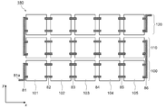
- FIG. 2 is a plan view of the back side of a solar cell grid in which a plurality of back junction cells are arranged in a grid.
- the solar cell strings 100, 110, 120 in which a plurality of cells are connected along the first direction (x direction) are arranged along the second direction (y direction) orthogonal to the first direction. Is arranged in.
- the solar cell string 100 includes a plurality of cells 101 to 105 arranged in the first direction.
- a solar cell string is formed by electrically connecting the electrodes provided on the back side of the cell via the wiring members 82 to 85.
- a plurality of cells are connected in series by connecting the p-side electrode of one of the two adjacent cells and the n-side electrode of the other cell via a wiring material.
- the cells can be connected in parallel by connecting the n-side electrodes or the p-side electrodes of adjacent cells.
- the wiring member 81 disposed at one end in the first direction includes a lead wire 81a that can be connected to an external circuit.
- the wiring member 86 arranged at the other end in the first direction is connected to the solar cell string 110 adjacent in the second direction.
- FIG. 3 is a schematic perspective view of the solar cell string 100.
- adjacent cells are connected by two wiring members.
- the number of wiring members arranged between adjacent cells is appropriately set according to the electrode pattern shape of the cells.
- the portions 831 and 841 located in the gaps between the adjacent solar cells of the wiring members 83 and 84 are exposed to the light receiving surface side, and thus are visible from the outside.
- a wiring material having at least a light receiving surface side of the wiring material metal reflection of the wiring material is reduced, and the exposed part of the wiring material and the cell are unified, and the solar cell module Designability is improved.
- the wiring material has a first main surface, a second main surface, and a side surface.
- the wiring material is a braided wire having a flat cross-sectional shape composed of a plurality of metal wires, and a conductive black layer is provided on the entire surface of the first main surface.
- the wiring material is arranged so that the first main surface is on the light receiving surface side, and the first main surface of the wiring material is connected to the back electrode of the cell.
- the width of the wiring material is, for example, about 1 mm to 5 mm, and the thickness of the wiring material is, for example, about 50 ⁇ m to 500 ⁇ m.
- the diameter of the metal wire constituting the braided wire is, for example, about 10 to 200 ⁇ m.
- the number of metal wires constituting the braided wire is about 10 to 500.
- the back junction cell since the back surfaces of adjacent cells are connected by a wiring material, shadowing loss does not become a problem even when the width (area) of the wiring material is large.
- the width of the wiring material as a flat shape, the contact area between the cell and the wiring material can be increased, and the contact resistance can be reduced. Further, by increasing the contact area between the cell and the wiring material, the adhesion reliability between the cell and the wiring material is increased, and the durability of the solar cell module is improved.
- a connection failure such as peeling of the wiring material occurs due to the difference in coefficient of linear expansion between the wiring material and the cell due to temperature change.
- Cheap a braided wire made of a plurality of strands is flexible and stretchable, so that stress resulting from the difference in linear expansion accompanying temperature change can be absorbed and dissipated by the wiring material. Therefore, even when the contact area between the cell and the wiring material is increased, high adhesion reliability can be maintained.
- the braided wire having a flat cross-sectional shape may be formed by knitting a plurality of metal strands so as to have a flat shape, and the braided wire obtained by knitting a plurality of strands into a cylindrical shape is converted into a flat cross-sectional shape by rolling. Also good.
- the method of knitting the metal wire flat knitting, single knitting, double knitting, triple knitting, denby knitting, cord knitting, atlas knitting, chain knitting, crochet, fourth knitting, sixth knitting, eighth knitting Examples include knitting, netting, iron wire, braiding, right tying, left tying, warp tying, weft tying, diagonal knitting, rubber knitting, koko knitting, knitting knitting, garter knitting and the like.
- the metal material constituting the metal strand is not particularly limited as long as it is conductive. In order to reduce electrical loss due to the resistance of the wiring material, it is preferable that the material of the wiring material has a low resistivity. Among these, copper or a copper alloy containing copper as a main component is preferable because the material is low cost.
- the wiring material is provided with a conductive black layer on at least the entire first main surface.
- a conductive black layer By providing the conductive black layer on the first main surface, light reflection at the portions 831 and 841 located in the gaps between the cells and exposed to the light receiving surface is reduced. Therefore, when the module is viewed from the light receiving surface side, the exposed portion of the wiring material and the cell color are unified.
- the visible light reflectance of the first main surface of the wiring material is preferably as small as the reflectance of the cell light receiving surface, and preferably 10% or less.
- the black layer described in this specification a desired visible light reflectance can be realized.
- the black layer is made of a conductive material containing a metal, it is difficult to completely eliminate surface reflection.
- the surface of the braided wire composed of a plurality of metal wires has irregularities due to the shape of the metal wires (generally a circular cross section), light is irregularly reflected on the surface of the wiring material. Therefore, the light reflected on the surface of the wiring member is visually recognized as haze-scattered light by the viewer on the light receiving surface side, and the reflected light with metallic luster is hardly visually recognized. Therefore, even if the light reflection at the wiring material cannot be completely suppressed, the designability due to the reflected light from the wiring material is unlikely to occur. If the light receiving surface of the cell is uneven, the reflected light on the light receiving surface of the cell and the reflected light on the first main surface of the wiring material consisting of the braided wire are approximated. The reflected light is inconspicuous and the design of the module is improved.
- a conductive black layer is provided on the first main surface not only in the exposed portions 831 and 841 between adjacent cells but also in the connection portions with the cells. Since the black layer provided for preventing light reflection has conductivity, the contact resistance between the cell electrode and the wiring material is small, and the power generation loss of the module can be reduced. Since the conductive black layer is provided on the entire first main surface of the wiring material, strict alignment is not required when connecting the cell and the wiring material. Therefore, productivity and yield of the solar cell module can be improved.
- the conductive black layer may also be provided on the side surface and the second main surface of the wiring material in the same manner as the first main surface.
- a non-blackening region where no conductive black layer is provided may be present in a portion not exposed on the surface of the wiring material.
- a braided wire having a conductive black layer can be obtained, for example, by subjecting a braided wire made of a metal strand to a conductive blackening treatment.
- a metal wire subjected to conductive blackening treatment may be knitted to form a braided wire.
- a dry process such as a sputtering method, a CVD method or a vacuum deposition method; a wet process such as application of a metal paste material, electrolytic plating or electroless plating (self-catalytic plating or displacement plating) is applied. Is possible.
- the material of the conductive black layer provided on the surface of the wiring material an alloy of copper and nickel, chromium, zinc, palladium or the like, metal palladium or palladium alloy, metal oxide, carbon nanotube or carbon in the metal, etc.
- distributed black material are mentioned.
- electroless plating As a method of providing a metal layer containing palladium on a wiring material (or a metal wire constituting the wiring material), electroless plating is preferable.
- the electroless plating solution for example, an aqueous solution containing a palladium salt, a halide ion, and a nitrogen-containing compound is used.
- the electroless plating solution is preferably an acidic aqueous solution having a pH of about 0 to 5.
- the palladium salt examples include palladium chloride, palladium sulfate, palladium oxide, palladium iodide, palladium bromide, palladium nitrate, palladium acetate, tetraammine palladium chloride, dinitrodiammine palladium, dichlorodiethylenediamine palladium, and the like.
- the palladium concentration in the electroless plating solution is preferably about 0.001 to 5 g / L.
- halide ion examples include chloride ion, bromide ion and iodide ion, and chloride ion is preferable.
- a halide ion source for containing halide ions in an electroless plating solution Hydrohalic acids such as hydrochloric acid, hydrobromic acid and hydroiodic acid; alkali metal salts such as sodium chloride and potassium bromide; alkaline earth metal salts such as magnesium chloride and calcium iodide; ammonium chloride and ammonium bromide And ammonium halides.
- the halide ion concentration in the electroless plating solution is preferably about 1 to 300 g / L.
- polyamines such as alkylene diamine, polyalkylene polyamine, polyamide polyamine, and crosslinked product of polyamide polyamine are preferable.
- the content of the nitrogen-containing compound in the electroless plating solution is preferably about 0.01 to 200 g / L.
- a conductive black layer (electroless palladium plating layer) containing palladium is provided by bringing the electroless plating solution into contact with a blackening treatment material (wiring material or metal element wire).
- a blackening treatment material wiring material or metal element wire.
- the electroless plating solution may be brought into contact with the blackening treatment material by immersing the blackening treatment material in the electroless plating solution.
- An electroless plating solution may be sprayed on the surface of the blackening treatment material.
- a conductive black layer is provided on the entire surface of the first main surface, side surface and second main surface, that is, the entire exposed portion of the surface of the metal strand.
- the obtained wiring material is obtained.
- a conductive black layer is also provided on the portion of the metal wire that is not exposed on the surface of the wiring material.
- the electroless plating solution is difficult to penetrate inside and is exposed on the braided wire surface of the metal strands.
- a black layer is provided in a region (first main surface of the exposed portions 831 and 841) that is visible from the outside of the wiring member.
- the portion of the wire that is not exposed on the surface of the wiring material may be a blackened region or a non-blackened region.
- the treatment temperature for electroless plating is preferably about 10 to 60 ° C., for example, and more preferably about 20 to 50 ° C.
- the treatment time is preferably about 10 seconds to 10 minutes, for example.
- a degreasing treatment, an acid treatment, or the like may be performed as necessary for the purpose of removing dirt and oxide film on the surface of the material to be plated.
- the plating material after electroless plating may be washed and dried as necessary.
- a wiring material composed of a back junction cell and a braided wire subjected to blackening treatment is prepared, and adjacent cells are connected to each other via the wiring material to produce a solar cell string.
- the back electrode of the cell and the first main surface of the wiring member are connected via a conductive connection material such as solder, a conductive film, or a conductive paste.
- solder When solder is used as the conductive connection material, a material obtained by welding solder in advance on the first main surface of the wiring material or on the electrode of the cell may be used. When solder is fused in advance onto the first main surface of the wiring material, if the solder adheres to the exposed portions 831 and 841 between adjacent cells, the metallic luster of the solder is visually recognized from the light receiving surface of the module, and the design property is improved. descend.
- the solder fusion area on the wiring material is adjusted so that the solder does not protrude into the visual recognition area, and the wiring material is connected when the solder is connected.
- the method of providing solder on the electrode of the cell and connecting the wiring material thereon does not require exact alignment for the purpose of preventing the solder from protruding to the exposed portion of the wiring material between the cells. Therefore, it is preferable to provide fusion solder, solder paste, or the like on the electrode of the cell to connect the electrode and the wiring material.
- a solder connection pad When connecting the cell and the wiring material by soldering, a solder connection pad may be arranged in a portion where the finger electrodes on the periphery in the cell surface are gathered, and the wiring material may be connected thereon.
- a wiring material composed of a braided wire of a plurality of metal strands molten solder tends to stay in the space between the metal strands due to capillary action. Therefore, the spread of the solder is suppressed, and the solder does not easily protrude from the exposed portion of the wiring material between the cells. Since it is difficult for the solder to spread, the area of the solder connection pad may be reduced.
- a wiring material made of a plate-like metal member used for a general module is rigid, if the area of the solder connection pad is reduced, it may be difficult to align the wiring material and the solder connection pad.
- the braided wire made of a plurality of strands is flexible and stretchable, even when a positional deviation occurs between adjacent cells, the wiring material is aligned on the solder connection pad by bending the wiring material. Can be implemented.
- the wiring material made of braided wire is flexible and stretchable, it can also be used for alignment in the string connection direction (x direction). Wiring material made of braided wire is also bent in the cell thickness direction (z direction), so it is possible to dissipate stress in the thickness direction and connect multiple cells even when the cells are warped Problems such as breakage when handling a subsequent string can be suppressed.
- a solar cell string in which a plurality of cells are connected via a wiring material is sandwiched between a light-receiving surface protection material 91 and a back surface protection material 92 via a sealing material 95, thereby forming a solar cell module. It is preferable to cure the encapsulant by heating a laminated body in which the light-receiving surface sealing material, the solar cell string, the back surface sealing material, and the back surface protecting material are sequentially placed on the light-receiving surface protection material. . Prior to sealing, a plurality of solar cell strings may be connected to form a solar cell grid as shown in FIG.
- a polyethylene resin composition mainly composed of an olefin elastomer, polypropylene, ethylene / ⁇ -olefin copolymer, ethylene / vinyl acetate copolymer (EVA), ethylene / vinyl acetate / triallyl. It is preferable to use a transparent resin such as isocyanurate (EVAT), polyvinyl butyrate (PVB), silicon, urethane, acrylic, or epoxy.
- EVAT isocyanurate
- PVB polyvinyl butyrate
- silicon silicon
- urethane acrylic
- epoxy epoxy
- the light-receiving surface protective material 91 is light transmissive, and glass, transparent plastic, or the like is used.
- As the back surface protective material 92 a black sheet whose main surface on the light receiving surface side is black is used. By using a black sheet as the back surface protection material, in addition to the cells, both the wiring material and the back surface protection material exposed between adjacent cells are unified in black, so the entire surface is unified in black and highly designed A module is obtained.
- the black sheet for example, a sheet including a black resin layer is used.
- the black resin layer has a visible light absorptivity and mainly absorbs visible light having a wavelength of 800 nm or less.
- the visible light transmittance of the black resin layer is preferably 10% or less.
- a resin composition containing a polyolefin resin, a polyester resin, an acrylic resin, a fluororesin, a thermoplastic resin such as an ethylene / vinyl acetate resin, and a colorant such as a pigment or a dye is preferably used.
- the black sheet used as the back surface protective material 92 may absorb visible light while having infrared reflectivity.
- a back surface protective material having infrared reflectivity By using a back surface protective material having infrared reflectivity, infrared light contained in light passing through a gap between adjacent cells or light transmitted through the cells can be reflected to the light receiving surface side and used for power generation.
- a black sheet which has infrared reflectivity what laminated
- the infrared reflective layer a resin layer made of a resin composition containing a white pigment having infrared reflectivity such as titanium oxide, an infrared reflective metal foil (for example, aluminum, silver), or the like is used.
- the tolerance of cell electrode patterning accuracy and alignment accuracy can be increased, and damage during handling can be suppressed, so module manufacturing efficiency and yield can be reduced. It can be improved. Further, as described above, in the completed module, the stress caused by the difference in the linear expansion coefficient due to the temperature change can be absorbed and dissipated by the wiring material made of the braided wire. Therefore, even when subjected to a temperature cycle test, poor connection of wiring materials due to dimensional changes or the like hardly occurs, and a module having excellent durability can be obtained.
- Black wire is applied to a braided wire with a flat cross section (width: about 2 mm, thickness: about 200 ⁇ m) knitted from a total of 64 copper wires with a diameter of about 60 ⁇ m as a unit, and evaluation is carried out did.
- Example 1 the above braided wire was immersed in an electroless palladium plating solution containing 0.5 g / L of palladium ("OPC Black Copper” manufactured by Okuno Pharmaceutical Co., Ltd.), and electroless plating was performed at room temperature. A braided wire having a conductive black layer on the entire surface was obtained. The strands inside the braided wire were not provided with a conductive black layer, and copper was exposed. The obtained braided wire had a black surface as a whole and exhibited good solder wettability similar to that of the braided wire before blackening treatment.
- OPC Black Copper manufactured by Okuno Pharmaceutical Co., Ltd.
- the above braided wire was subjected to black chrome treatment example 2, black nickel treatment example 3 and black oxide treatment (formation of fine concavo-convex film of copper oxide) 4 by strong alkali boiling. Evaluation similar to Example 1 was performed. In Examples 2 to 4, the entire surface of the wiring material was black, but showed no solder wetting.
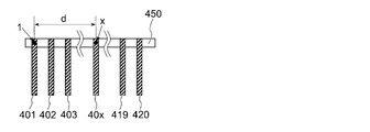
- the position where the other terminal is brought into contact is sequentially changed on the wiring members 402 to 420, the resistance is measured, the inter-terminal distance d and the resistance are plotted, and linear approximation by the least square method is performed.
- the contact resistance when a plate-like copper foil having a width of 1.5 mm was used as the wiring material was 2.3 times that when the braided wire not subjected to blackening treatment was used as the wiring material.
- the contact resistance when using the braided wire subjected to the blackening treatment of Example 1 as the wiring material is 1.1 times that of the braided wire not subjected to the blackening treatment, and the contact resistance before and after the blackening treatment There was no significant change in resistance.
- the wiring material made of braided wire has lower contact resistance with the electrode material during solder connection than the plate-like wiring material, and the characteristics are maintained even in the braided wire that has been blackened with palladium. You can see that.
Abstract
A solar cell module (200) is provided with a solar cell string in which a plurality of backside-bonded solar cells (102, 103, 104) are electrically connected by wiring material (83, 84). On a light reception surface side of the solar cell string, an optically transmissive light reception surface protection material (91) is disposed, and on a backside of the solar cell string, a backside protection material (92) is disposed. The wiring material is a braided wire having a flat cross sectional shape comprising a plurality of metal strands. A first major surface of the wiring material is connected to a metal electrode of the backside-bonded solar cells. The wiring material has an electrically conductive black-colored layer on the entire first major surface thereof.
Description
本発明は、太陽電池モジュールに関する。
The present invention relates to a solar cell module.
単結晶シリコン基板や多結晶シリコン基板等の結晶半導体基板を用いた太陽電池は、1つの基板の面積が小さいため、実用に際しては、複数の太陽電池を電気的に接続してモジュール化を行い、出力を高めている。金属箔等からなる配線材を、はんだや導電性接着剤等を介して太陽電池の電極に接続することにより、隣接する太陽電池間の電気的接続が行われる。配線材を介して複数の太陽電池が接続された太陽電池ストリングを、受光面保護材と裏面保護材との間で封止することにより太陽電池モジュールが得られる。
A solar cell using a crystalline semiconductor substrate such as a single crystal silicon substrate or a polycrystalline silicon substrate has a small area of one substrate. Therefore, in practical use, a plurality of solar cells are electrically connected and modularized. The output is increased. By connecting a wiring material made of metal foil or the like to the electrode of the solar cell via solder, a conductive adhesive or the like, electrical connection between adjacent solar cells is performed. A solar cell module is obtained by sealing a solar cell string to which a plurality of solar cells are connected via a wiring material between a light-receiving surface protective material and a back surface protective material.
裏面接合太陽電池は、受光面に金属電極が設けられていないため、受光面側から視認した場合は黒色を呈している。裏面接合太陽電池のモジュール化においては、隣接する太陽電池の裏面の電極同士が配線材により電気的に接続される。
Since the back junction solar cell is not provided with a metal electrode on the light receiving surface, it is black when viewed from the light receiving surface side. In modularization of a back junction solar cell, electrodes on the back surface of adjacent solar cells are electrically connected by a wiring material.
裏面接合太陽電池を用いた太陽電池モジュールにおける裏面保護材として、黒色のシートを用いれば、太陽電池モジュールを受光面から視認した場合に、太陽電池および太陽電池間の隙間が黒色で統一され、意匠性が高められる。一方、隣接する太陽電池間を接続する配線材は金属光沢を有するため、建物の屋根や壁面に太陽電池モジュールを設置した場合、配線材に照射された太陽光の反射光が視認され、意匠性が損なわれる場合がある。
When a black sheet is used as a back surface protection material in a solar cell module using a back junction solar cell, when the solar cell module is viewed from the light receiving surface, the gap between the solar cell and the solar cell is unified in black, and the design Sexuality is enhanced. On the other hand, since the wiring material connecting adjacent solar cells has a metallic luster, when a solar cell module is installed on the roof or wall of a building, reflected light of sunlight irradiated on the wiring material is visually recognized, and the design property May be damaged.
特許文献1では、配線材の受光面側に露出する部分を着色樹脂層で被覆することにより、配線材の金属光沢による意匠性の低下を抑制することが提案されている。特許文献2では、隣接する太陽電池の間に絶縁テープ等からなるシールドを設けることにより、受光面側からの配線材の視認を遮って、モジュールの意匠性を高めている。
In Patent Document 1, it is proposed that a portion exposed on the light receiving surface side of a wiring material is covered with a colored resin layer to suppress a decrease in design properties due to the metallic luster of the wiring material. In Patent Document 2, by providing a shield made of an insulating tape or the like between adjacent solar cells, the visual recognition of the wiring material from the light receiving surface side is blocked and the design of the module is improved.
特許文献1で提案されているように配線材を絶縁性の樹脂層で被覆する場合は、太陽電池の電極との非接続部分を選択的に被覆し、太陽電池の電極との接続部分が被覆されないように、配線材上の樹脂層をパターニングする必要がある。また、配線材と太陽電池との接続時には、樹脂層により被覆されていない部分が太陽電池の電極と接続されるように、位置合わせが必要となる。そのため、配線材の製造コストの増加、配線材接続時の位置合わせのための工数の増加、配線材や太陽電池モジュールの歩留まりの低下等が問題となる。
When the wiring material is covered with an insulating resin layer as proposed in Patent Document 1, the non-connection portion with the solar cell electrode is selectively covered, and the connection portion with the solar cell electrode is covered. In order to prevent this, it is necessary to pattern the resin layer on the wiring material. Further, when the wiring member and the solar cell are connected, alignment is necessary so that the portion not covered with the resin layer is connected to the electrode of the solar cell. For this reason, an increase in the manufacturing cost of the wiring material, an increase in the number of man-hours for alignment when connecting the wiring material, a decrease in the yield of the wiring material and the solar cell module, and the like become problems.
特許文献2のように隣接する太陽電池間にシールドを配置する構成では、太陽電池の端部において、太陽電池と配線材との間にシールドが挟持されている。そのため、太陽電池の電極と配線材との接触面積の低下や、配線材の曲げ応力等に起因して、太陽電池モジュールの出力が低下する場合があり、温度サイクル試験において出力の低下が顕著となる。
In the configuration in which the shield is disposed between adjacent solar cells as in Patent Document 2, the shield is sandwiched between the solar cell and the wiring material at the end of the solar cell. Therefore, the output of the solar cell module may decrease due to the decrease in the contact area between the electrode of the solar cell and the wiring material, the bending stress of the wiring material, etc. Become.
上記に鑑み、本発明は、受光面から視認した場合に全体が黒色で統一されて意匠性が高く、かつ温度変化等による出力低下が抑制され耐久性に優れる太陽電池モジュールの提供を目的とする。
In view of the above, an object of the present invention is to provide a solar cell module that is unified in black as a whole when viewed from the light receiving surface, has high designability, suppresses a decrease in output due to a temperature change or the like, and has excellent durability. .
本発明の太陽電池モジュールは、受光面および裏面を有する太陽電池の複数が配線材により電気的に接続された太陽電池ストリングを備える。太陽電池ストリングにおいて、太陽電池の裏面に設けられた金属電極と配線材の第一主面とは、例えば、はんだにより接続されている。太陽電池ストリングの受光面側には光透過性の受光面保護材が配置され、太陽電池ストリングの裏面には裏面保護材が配置されている。太陽電池ストリングは、受光面保護材と裏面保護材との間に充填された封止材により封止されている。
The solar cell module of the present invention includes a solar cell string in which a plurality of solar cells having a light receiving surface and a back surface are electrically connected by a wiring material. In the solar cell string, the metal electrode provided on the back surface of the solar cell and the first main surface of the wiring member are connected by, for example, solder. A light-transmitting light-receiving surface protective material is disposed on the light-receiving surface side of the solar cell string, and a back surface protective material is disposed on the back surface of the solar cell string. The solar cell string is sealed with a sealing material filled between the light-receiving surface protective material and the back surface protective material.
太陽電池は、受光面に金属電極を有さず、裏面にのみ金属電極が設けられた裏面接合太陽電池である。裏面保護材の受光面側の主面は黒色である。配線材は、複数の金属素線からなる断面扁平形状の編組線であり、配線材の第一主面が、太陽電池の金属電極と接続されている。配線材は、第一主面の全面に導電性黒色層が設けられている。
The solar cell is a back junction solar cell that does not have a metal electrode on the light receiving surface and is provided with a metal electrode only on the back surface. The main surface on the light receiving surface side of the back surface protective material is black. The wiring member is a braided wire having a flat cross-sectional shape composed of a plurality of metal strands, and the first main surface of the wiring member is connected to the metal electrode of the solar cell. The wiring material is provided with a conductive black layer on the entire first main surface.
配線材の金属素線の材料としては、銅または銅合金が好ましい。配線材の表面に設けられる導電性黒色層としては、パラジウムを含む金属層が好ましく、例えば、無電解メッキにより配線材の表面に設けられる。
As the material of the metal element wire of the wiring material, copper or copper alloy is preferable. As the conductive black layer provided on the surface of the wiring material, a metal layer containing palladium is preferable. For example, the conductive black layer is provided on the surface of the wiring material by electroless plating.
本発明の太陽電池モジュールは、受光面から視認した場合に、全面が黒色で統一されているため意匠性に優れる。また、太陽電池の電極と配線材との接触抵抗が小さいため、出力特性に優れる。さらに、配線材が柔軟性を有しているため、太陽電池モジュールは温度サイクル耐久性に優れる。
The solar cell module of the present invention is excellent in design because the entire surface is unified in black when viewed from the light receiving surface. Moreover, since the contact resistance between the electrode of the solar cell and the wiring material is small, the output characteristics are excellent. Furthermore, since the wiring material has flexibility, the solar cell module is excellent in temperature cycle durability.
[太陽電池モジュールの概略構成]
図1は、一実施形態の太陽電池モジュール(以下、「モジュール」と記載する)の模式的断面図である。図1に示すモジュール200は、複数の太陽電池102,103,104(以下、「セル」と記載する)が、配線材83,84を介して電気的に接続された太陽電池ストリングを備える。 [Schematic configuration of solar cell module]
FIG. 1 is a schematic cross-sectional view of a solar cell module (hereinafter referred to as “module”) according to an embodiment. Amodule 200 shown in FIG. 1 includes a solar cell string in which a plurality of solar cells 102, 103, and 104 (hereinafter referred to as “cells”) are electrically connected via wiring members 83 and 84.
図1は、一実施形態の太陽電池モジュール(以下、「モジュール」と記載する)の模式的断面図である。図1に示すモジュール200は、複数の太陽電池102,103,104(以下、「セル」と記載する)が、配線材83,84を介して電気的に接続された太陽電池ストリングを備える。 [Schematic configuration of solar cell module]
FIG. 1 is a schematic cross-sectional view of a solar cell module (hereinafter referred to as “module”) according to an embodiment. A
太陽電池ストリングの受光面側(図1の上側)には、受光面保護材91が設けられ、裏面側(図1の下側)には裏面保護材92が設けられている。モジュール200では、保護材91,92の間に封止材95が充填されることにより、太陽電池ストリングが封止されている。
The light receiving surface protective material 91 is provided on the light receiving surface side (upper side in FIG. 1) of the solar cell string, and the back surface protective material 92 is provided on the back surface side (lower side in FIG. 1). In the module 200, the solar cell string is sealed by filling the sealing material 95 between the protective materials 91 and 92.
セルとしては、裏面接合太陽電池(裏面接合セル)が用いられる。裏面接合セルは、結晶シリコン等の半導体基板の裏面側にp型半導体層およびn型半導体層を備え、p型半導体層上およびn型半導体層上のそれぞれに金属電極が設けられている。金属電極は、印刷やメッキ等の公知の方法により形成できる。例えば、Agペーストのスクリーン印刷により形成されたAg電極や、電解メッキにより形成された銅メッキ電極等が好ましく用いられる。
As the cell, a back junction solar cell (back junction cell) is used. The back junction cell includes a p-type semiconductor layer and an n-type semiconductor layer on the back side of a semiconductor substrate such as crystalline silicon, and a metal electrode is provided on each of the p-type semiconductor layer and the n-type semiconductor layer. The metal electrode can be formed by a known method such as printing or plating. For example, an Ag electrode formed by screen printing of Ag paste, a copper plating electrode formed by electrolytic plating, or the like is preferably used.
裏面接合セルは、半導体基板の受光面に金属電極を有さず、半導体基板で生成した光キャリア(正孔および電子)を、半導体基板の裏面側に設けられた金属電極により回収する。裏面接合セルは、受光面に金属電極を有していないため、受光面側から視認した際に、セルの全面が黒色系で統一されており、意匠性に優れる。セルの形状は特に限定されないが、一般には平面視矩形状である。矩形は正方形および長方形を含む。「矩形状」とは、完全な正方形または長方形である必要はなく、例えば、半導体基板の形状はセミスクエア型(矩形の角が丸みを帯びているものや、切欠き部が存在するもの)でもよい。
The backside junction cell does not have a metal electrode on the light receiving surface of the semiconductor substrate, and collects photocarriers (holes and electrons) generated on the semiconductor substrate with a metal electrode provided on the backside of the semiconductor substrate. Since the back junction cell does not have a metal electrode on the light receiving surface, the entire surface of the cell is unified in black when viewed from the light receiving surface side, and is excellent in design. The shape of the cell is not particularly limited, but is generally rectangular in plan view. A rectangle includes a square and a rectangle. The “rectangular shape” does not need to be a perfect square or rectangle. For example, the shape of the semiconductor substrate may be a semi-square type (a rectangular corner having a rounded corner or a notch). Good.
半導体基板に取り込まれる光量を増大させ、変換効率を向上するために、セルの受光面には、凹凸構造が設けられていることが好ましい。凹凸の形状は、四角錐形状(ピラミッド形状)が好ましい。ピラミッド形状の凹凸構造は、例えば、単結晶シリコン基板の表面に異方性エッチング処理を施すことにより形成される。セルの受光面に設けられる凹凸の高さは、例えば、0.5~10μm程度であり、好ましくは1~5μm程度である。セルの裏面にも凹凸構造が設けられていてもよい。
In order to increase the amount of light taken into the semiconductor substrate and improve the conversion efficiency, it is preferable that the light receiving surface of the cell is provided with an uneven structure. The uneven shape is preferably a quadrangular pyramid shape (pyramid shape). The pyramidal concavo-convex structure is formed, for example, by subjecting the surface of a single crystal silicon substrate to anisotropic etching. The height of the unevenness provided on the light receiving surface of the cell is, for example, about 0.5 to 10 μm, and preferably about 1 to 5 μm. An uneven structure may also be provided on the back surface of the cell.
図2は、複数の裏面接合セルがグリッド状に配置された太陽電池グリッドの裏面側の平面図である。太陽電池グリッド180では、第一方向(x方向)に沿って複数のセルが接続された太陽電池ストリング100,110,120が、第一方向と直交する第二方向(y方向)に沿って並んで配置されている。
FIG. 2 is a plan view of the back side of a solar cell grid in which a plurality of back junction cells are arranged in a grid. In the solar cell grid 180, the solar cell strings 100, 110, 120 in which a plurality of cells are connected along the first direction (x direction) are arranged along the second direction (y direction) orthogonal to the first direction. Is arranged in.
太陽電池ストリング100は、第一方向に沿って並んだ複数のセル101~105を備える。セルの裏面側に設けられた電極を、配線材82~85を介して電気的に接続することにより、太陽電池ストリングが形成される。隣接する2つのセルのうちの一方のセルのp側電極と他方のセルのn側電極とを配線材を介して接続することにより、複数のセルが直列に接続される。隣接するセルのn側電極同士またはp側電極同士を接続することにより、セルを並列接続することもできる。
The solar cell string 100 includes a plurality of cells 101 to 105 arranged in the first direction. A solar cell string is formed by electrically connecting the electrodes provided on the back side of the cell via the wiring members 82 to 85. A plurality of cells are connected in series by connecting the p-side electrode of one of the two adjacent cells and the n-side electrode of the other cell via a wiring material. The cells can be connected in parallel by connecting the n-side electrodes or the p-side electrodes of adjacent cells.
太陽電池ストリング100において、第一方向の一方の端部に配置された配線材81は、外部回路と接続可能な引き出し線81aを備える。第一方向の他方の端部に配置された配線材86は、第二方向に隣接する太陽電池ストリング110と接続されている。
In the solar cell string 100, the wiring member 81 disposed at one end in the first direction includes a lead wire 81a that can be connected to an external circuit. The wiring member 86 arranged at the other end in the first direction is connected to the solar cell string 110 adjacent in the second direction.
図3は、太陽電池ストリング100の概略斜視図である。図3では、隣接するセル同士が2本の配線材により接続されている。隣接するセル間に配置される配線材の数は、セルの電極パターン形状等に応じて適宜に設定される。
FIG. 3 is a schematic perspective view of the solar cell string 100. In FIG. 3, adjacent cells are connected by two wiring members. The number of wiring members arranged between adjacent cells is appropriately set according to the electrode pattern shape of the cells.
太陽電池モジュールにおいて、配線材83,84の隣接する太陽電池間の隙間に位置する部分831,841は、受光面側に露出しているため、外部から視認される。以下に詳述するように、少なくとも受光面側が黒色である配線材を用いることにより、配線材の金属反射が低減し、配線材の露出部分とセルとの視感が統一され、太陽電池モジュールの意匠性が高められる。
In the solar cell module, the portions 831 and 841 located in the gaps between the adjacent solar cells of the wiring members 83 and 84 are exposed to the light receiving surface side, and thus are visible from the outside. As will be described in detail below, by using a wiring material having at least a light receiving surface side of the wiring material, metal reflection of the wiring material is reduced, and the exposed part of the wiring material and the cell are unified, and the solar cell module Designability is improved.
[配線材]
配線材は、第一主面、第二主面および側面を有する。配線材は、複数の金属素線からなる断面扁平形状の編組線であり、第一主面の全面に導電性黒色層が設けられている。太陽電池ストリングでは、第一主面が受光面側となるように配線材が配置され、配線材の第一主面がセルの裏面電極と接続される。 [Wiring material]
The wiring material has a first main surface, a second main surface, and a side surface. The wiring material is a braided wire having a flat cross-sectional shape composed of a plurality of metal wires, and a conductive black layer is provided on the entire surface of the first main surface. In the solar cell string, the wiring material is arranged so that the first main surface is on the light receiving surface side, and the first main surface of the wiring material is connected to the back electrode of the cell.
配線材の幅は、例えば1mm~5mm程度であり、配線材の厚みは例えば50μm~500μm程度である。編組線を構成する金属素線の直径は、例えば10~200μm程度である。編組線を構成する金属素線の数は10~500本程度である。
The width of the wiring material is, for example, about 1 mm to 5 mm, and the thickness of the wiring material is, for example, about 50 μm to 500 μm. The diameter of the metal wire constituting the braided wire is, for example, about 10 to 200 μm. The number of metal wires constituting the braided wire is about 10 to 500.
裏面接合セルでは、隣接するセルの裏面同士を配線材により接続するため、配線材の幅(面積)が大きい場合でもシャドーイングロスは問題とならない。配線材を扁平形状として幅を大きくすることにより、セルと配線材との接触面積を増大し、接触抵抗を低減できる。また、セルと配線材との接触面積を増大させることにより、セルと配線材との接着信頼性が高められ、太陽電池モジュールの耐久性が向上する。
In the back junction cell, since the back surfaces of adjacent cells are connected by a wiring material, shadowing loss does not become a problem even when the width (area) of the wiring material is large. By increasing the width of the wiring material as a flat shape, the contact area between the cell and the wiring material can be increased, and the contact resistance can be reduced. Further, by increasing the contact area between the cell and the wiring material, the adhesion reliability between the cell and the wiring material is increased, and the durability of the solar cell module is improved.
一般的なモジュールに用いられる板状の配線材とセルとの接触面積が増大すると、温度変化による配線材とセルとの線膨張係数の相違に起因して配線材の剥がれ等の接続不良が生じやすい。一方、複数の素線からなる編組線は、柔軟で伸縮性を有するため、温度変化に伴う線膨張の相違に起因する応力を、配線材により吸収・散逸できる。そのため、セルと配線材との接触面積を増大させた場合でも、高い接着信頼性を維持できる。
When the contact area between a plate-like wiring material used in a general module and a cell increases, a connection failure such as peeling of the wiring material occurs due to the difference in coefficient of linear expansion between the wiring material and the cell due to temperature change. Cheap. On the other hand, a braided wire made of a plurality of strands is flexible and stretchable, so that stress resulting from the difference in linear expansion accompanying temperature change can be absorbed and dissipated by the wiring material. Therefore, even when the contact area between the cell and the wiring material is increased, high adhesion reliability can be maintained.
断面扁平形状の編組線は、扁平形状となるように複数の金属素線を編むことにより形成してもよく、複数の素線を円筒形状に編んだ編組線を、圧延加工により断面扁平形状としてもよい。金属素線の編み方としては、平編み、一重編組、二重編組、三重編組、デンビー編み、コード編み、アトラス編み、鎖編み、かぎ編み、四つ目編み、六つ目編み、八つ目編み、網代、鉄線、三つ編み、右結び、左結び、たて巻き結び、よこ巻き結び、斜め編み、ゴム編み、かのこ編み、メリヤス編み、ガーター編み等が挙げられる。
The braided wire having a flat cross-sectional shape may be formed by knitting a plurality of metal strands so as to have a flat shape, and the braided wire obtained by knitting a plurality of strands into a cylindrical shape is converted into a flat cross-sectional shape by rolling. Also good. As for the method of knitting the metal wire, flat knitting, single knitting, double knitting, triple knitting, denby knitting, cord knitting, atlas knitting, chain knitting, crochet, fourth knitting, sixth knitting, eighth knitting Examples include knitting, netting, iron wire, braiding, right tying, left tying, warp tying, weft tying, diagonal knitting, rubber knitting, koko knitting, knitting knitting, garter knitting and the like.
金属素線を構成する金属材料は、導電性であれば特に限定されない。配線材の抵抗に起因する電気的ロスを低減するために、配線材の材料は低抵抗率であることが好ましい。中でも、材料が低コストであることから、銅、または銅を主成分とする銅合金が好ましい。
The metal material constituting the metal strand is not particularly limited as long as it is conductive. In order to reduce electrical loss due to the resistance of the wiring material, it is preferable that the material of the wiring material has a low resistivity. Among these, copper or a copper alloy containing copper as a main component is preferable because the material is low cost.
(導電性黒色層)
配線材は、少なくとも第一主面の全面に導電性黒色層が設けられている。第一主面に導電性黒色層が設けられることにより、セルの隙間に位置して受光面に露出する部分831,841での光反射が低減する。そのため、受光面側からモジュールを視認した場合に、配線材の露出部分とセルの色目が統一される。 (Conductive black layer)
The wiring material is provided with a conductive black layer on at least the entire first main surface. By providing the conductive black layer on the first main surface, light reflection at the portions 831 and 841 located in the gaps between the cells and exposed to the light receiving surface is reduced. Therefore, when the module is viewed from the light receiving surface side, the exposed portion of the wiring material and the cell color are unified.
配線材は、少なくとも第一主面の全面に導電性黒色層が設けられている。第一主面に導電性黒色層が設けられることにより、セルの隙間に位置して受光面に露出する部分831,841での光反射が低減する。そのため、受光面側からモジュールを視認した場合に、配線材の露出部分とセルの色目が統一される。 (Conductive black layer)
The wiring material is provided with a conductive black layer on at least the entire first main surface. By providing the conductive black layer on the first main surface, light reflection at the
モジュールの全体を黒色で統一する観点からは、配線材の第一主面の可視光反射率はセル受光面の反射率と同等に小さいことが好ましく、10%以下が好ましい。本明細書に記載の黒色層を設けることにより、所望の可視光反射率を実現できる。一方、黒色層は金属を含む導電性材料からなるため、表面反射を完全に排除することは困難である。
From the viewpoint of unifying the entire module in black, the visible light reflectance of the first main surface of the wiring material is preferably as small as the reflectance of the cell light receiving surface, and preferably 10% or less. By providing the black layer described in this specification, a desired visible light reflectance can be realized. On the other hand, since the black layer is made of a conductive material containing a metal, it is difficult to completely eliminate surface reflection.
複数の金属素線からなる編組線の表面は、金属素線の形状(一般には断面円形)に起因する凹凸を有するため、配線材の表面では光が乱反射される。そのため、配線材の表面で反射された光は、受光面側の視認者にはヘイズのかかった散乱光として視認され、金属光沢を帯びた反射光はほとんど視認されない。したがって、配線材での光反射を完全に抑制できない場合であっても、配線材からの反射光に起因する意匠性の低下が生じ難い。セルの受光面に凹凸が形成されている場合は、セルの受光面での反射光と編組線からなる配線材の第一主面での反射光の視感が近似するため、配線材からの反射光が目立たず、モジュールの意匠性が高められる。
Since the surface of the braided wire composed of a plurality of metal wires has irregularities due to the shape of the metal wires (generally a circular cross section), light is irregularly reflected on the surface of the wiring material. Therefore, the light reflected on the surface of the wiring member is visually recognized as haze-scattered light by the viewer on the light receiving surface side, and the reflected light with metallic luster is hardly visually recognized. Therefore, even if the light reflection at the wiring material cannot be completely suppressed, the designability due to the reflected light from the wiring material is unlikely to occur. If the light receiving surface of the cell is uneven, the reflected light on the light receiving surface of the cell and the reflected light on the first main surface of the wiring material consisting of the braided wire are approximated. The reflected light is inconspicuous and the design of the module is improved.
配線材83,84の第一主面では、隣接するセル間の露出部分831,841だけでなく、セルとの接続部分においても、第一主面に導電性黒色層が設けられている。光反射防止のために設けられる黒色層が導電性を有しているため、セルの電極と配線材との接触抵抗が小さく、モジュールの発電ロスを低減できる。配線材の第一主面の全面に導電性黒色層が設けられているため、セルと配線材とを接続する際に、厳密な位置合わせを必要としない。そのため、太陽電池モジュールの生産性および歩留まりを向上できる。
On the first main surface of the wiring members 83 and 84, a conductive black layer is provided on the first main surface not only in the exposed portions 831 and 841 between adjacent cells but also in the connection portions with the cells. Since the black layer provided for preventing light reflection has conductivity, the contact resistance between the cell electrode and the wiring material is small, and the power generation loss of the module can be reduced. Since the conductive black layer is provided on the entire first main surface of the wiring material, strict alignment is not required when connecting the cell and the wiring material. Therefore, productivity and yield of the solar cell module can be improved.
配線材の側面および第二主面にも、第一主面と同様に導電性黒色層が設けられていてもよい。配線材の表面に露出していない部分には、導電性黒色層が設けられていない非黒色化処理領域が存在してもよい。
The conductive black layer may also be provided on the side surface and the second main surface of the wiring material in the same manner as the first main surface. A non-blackening region where no conductive black layer is provided may be present in a portion not exposed on the surface of the wiring material.
導電性黒色層を有する編組線は、例えば、金属素線を編んだ編組線に導電性黒色化処理を施すことにより得られる。導電性黒色化処理を施した金属素線を編んで編組線としてもよい。導電性黒色層の形成は、例えば、スパッタ法、CVD法、真空蒸着法等のドライプロセス;金属ペースト材料の塗布、電解メッキまたは無電解メッキ(自己触媒メッキもしくは置換メッキ)等のウェットプロセスを適用可能である。
A braided wire having a conductive black layer can be obtained, for example, by subjecting a braided wire made of a metal strand to a conductive blackening treatment. A metal wire subjected to conductive blackening treatment may be knitted to form a braided wire. For the formation of the conductive black layer, for example, a dry process such as a sputtering method, a CVD method or a vacuum deposition method; a wet process such as application of a metal paste material, electrolytic plating or electroless plating (self-catalytic plating or displacement plating) is applied. Is possible.
配線材の表面に設けられる導電性黒色層の材料としては、銅と、ニッケル、クロム、亜鉛、パラジウム等との合金、金属パラジウムまたはパラジウム合金、金属酸化物、金属中にカーボンナノチューブやカーボン等の黒色材料を分散させたもの等が挙げられる。中でも、導電性に優れ、銅等の金属材料との密着性に優れ、かつはんだに対する濡れ性が高いことから、導電性黒色層としてパラジウムを含む金属層を設けることが好ましい。
As the material of the conductive black layer provided on the surface of the wiring material, an alloy of copper and nickel, chromium, zinc, palladium or the like, metal palladium or palladium alloy, metal oxide, carbon nanotube or carbon in the metal, etc. The thing etc. which disperse | distributed black material are mentioned. Especially, since it is excellent in electroconductivity, adhesiveness with metal materials, such as copper, and wettability with respect to solder is high, it is preferable to provide the metal layer containing palladium as an electroconductive black layer.
配線材(または配線材を構成する金属素線)にパラジウムを含む金属層を設ける方法としては、無電解メッキが好ましい。無電解メッキ液としては、例えば、パラジウム塩、ハロゲン化物イオン、および窒素含有化合物を含む水溶液が用いられる。無電解メッキ液は、pHが0~5程度の酸性水溶液であることが好ましい。
As a method of providing a metal layer containing palladium on a wiring material (or a metal wire constituting the wiring material), electroless plating is preferable. As the electroless plating solution, for example, an aqueous solution containing a palladium salt, a halide ion, and a nitrogen-containing compound is used. The electroless plating solution is preferably an acidic aqueous solution having a pH of about 0 to 5.
パラジウム塩としては、塩化パラジウム、硫酸パラジウム、酸化パラジウム、ヨウ化パラジウム、臭化パラジウム、硝酸パラジウム、酢酸パラジウム、テトラアンミンパラジウムクロライド、ジニトロジアンミンパラジウム、ジクロロジエチレンジアミンパラジウム等が挙げられる。無電解メッキ液中のパラジウム濃度は、0.001~5g/L程度が好ましい。
Examples of the palladium salt include palladium chloride, palladium sulfate, palladium oxide, palladium iodide, palladium bromide, palladium nitrate, palladium acetate, tetraammine palladium chloride, dinitrodiammine palladium, dichlorodiethylenediamine palladium, and the like. The palladium concentration in the electroless plating solution is preferably about 0.001 to 5 g / L.
ハロゲン化物イオンとしては、塩化物イオン、臭化物イオンおよびヨウ化物イオンが挙げられ、塩化物イオンが好ましい。無電解メッキ液中にハロゲン化物イオンを含有させるためのハロゲン化物イオン源としては。塩酸、臭化水素酸、ヨウ化水素酸等のハロゲン化水素酸;塩化ナトリウム、臭化カリウム等のアルカリ金属塩;塩化マグネシウム、ヨウ化カルシウム等のアルカリ土類金属塩;塩化アンモニウム、臭化アンモニウム等のハロゲン化アンモニウム等が挙げられる。無電解メッキ液中のハロゲン化物イオン濃度は、1~300g/L程度が好ましい。
Examples of the halide ion include chloride ion, bromide ion and iodide ion, and chloride ion is preferable. What is a halide ion source for containing halide ions in an electroless plating solution? Hydrohalic acids such as hydrochloric acid, hydrobromic acid and hydroiodic acid; alkali metal salts such as sodium chloride and potassium bromide; alkaline earth metal salts such as magnesium chloride and calcium iodide; ammonium chloride and ammonium bromide And ammonium halides. The halide ion concentration in the electroless plating solution is preferably about 1 to 300 g / L.
窒素含有化合物としては、アルキレンジアミン、ポリアルキレンポリアミン、ポリアミドポリアミン、ポリアミドポリアミンの架橋化物等のポリアミン類が好ましい。無電解メッキ液中の窒素含有化合物の含有量は、0.01~200g/L程度が好ましい。
As the nitrogen-containing compound, polyamines such as alkylene diamine, polyalkylene polyamine, polyamide polyamine, and crosslinked product of polyamide polyamine are preferable. The content of the nitrogen-containing compound in the electroless plating solution is preferably about 0.01 to 200 g / L.
被黒色化処理材料(配線材または金属素線)に上記の無電解メッキ液を接触させることにより、パラジウムを含む導電性黒色層(無電解パラジウムメッキ層)が設けられる。例えば、被黒色化処理材料を無電解メッキ液に浸漬することにより、被黒色化処理材料に無電解メッキ液を接触させればよい。被黒色化処理材料の表面に無電解メッキ液をスプレーしてもよい。
A conductive black layer (electroless palladium plating layer) containing palladium is provided by bringing the electroless plating solution into contact with a blackening treatment material (wiring material or metal element wire). For example, the electroless plating solution may be brought into contact with the blackening treatment material by immersing the blackening treatment material in the electroless plating solution. An electroless plating solution may be sprayed on the surface of the blackening treatment material.
金属素線を編んだ編組線を無電解メッキ液に浸漬すると、第一主面、側面および第二主面の全面、すなわち金属素線の表面への露出部分の全体に導電性黒色層が設けられた配線材が得られる。無電解メッキ液が編組線の内部にも十分浸透する場合は、金属素線の配線材の表面に露出していない部分にも導電性黒色層が設けられる。
When a braided wire knitted with metal strands is immersed in an electroless plating solution, a conductive black layer is provided on the entire surface of the first main surface, side surface and second main surface, that is, the entire exposed portion of the surface of the metal strand. The obtained wiring material is obtained. When the electroless plating solution sufficiently penetrates into the braided wire, a conductive black layer is also provided on the portion of the metal wire that is not exposed on the surface of the wiring material.
一方、編組線の編み密度が高い場合や、金属素線の無電解メッキ液に対する濡れ性が小さい場合は、内部に無電解メッキ液が浸透し難く、金属素線の編組線表面に露出していない部分は、導電性黒色層が設けられていない非黒色化処理領域となる。太陽電池モジュールの全面を黒色で統一するとの目的においては、配線材の外部から視認される領域(露出部分831,841の第一主面)に黒色層が設けられていればよいため、金属素線の配線材の表面に露出していない部分は、黒色化処理領域でも非黒色化処理領域でもよい。
On the other hand, when the braided wire has a high knitting density or when the wettability of the metal strands to the electroless plating solution is small, the electroless plating solution is difficult to penetrate inside and is exposed on the braided wire surface of the metal strands. The part which does not become a non-blackening process area | region where the electroconductive black layer is not provided. For the purpose of unifying the entire surface of the solar cell module in black, it is sufficient that a black layer is provided in a region (first main surface of the exposed portions 831 and 841) that is visible from the outside of the wiring member. The portion of the wire that is not exposed on the surface of the wiring material may be a blackened region or a non-blackened region.
無電解メッキの処理温度は、例えば10~60℃程度が好ましく、20~50℃程度がより好ましい。処理時間は、例えば、10秒~10分程度が好ましい。
The treatment temperature for electroless plating is preferably about 10 to 60 ° C., for example, and more preferably about 20 to 50 ° C. The treatment time is preferably about 10 seconds to 10 minutes, for example.
無電解メッキにより導電性黒色化処理を施す前に、必要に応じて、被メッキ処理材料の表面の汚れや酸化皮膜を除去する目的で、脱脂処理、酸処理等を実施してもよい。無電解メッキ後のメッキ処理材料は、必要に応じて水洗および乾燥を行ってもよい。
Before performing the conductive blackening treatment by electroless plating, a degreasing treatment, an acid treatment, or the like may be performed as necessary for the purpose of removing dirt and oxide film on the surface of the material to be plated. The plating material after electroless plating may be washed and dried as necessary.
[太陽電池モジュールの形成]
モジュールの作製においては、まず、裏面接合セルおよび黒色化処理が施された編組線からなる配線材を準備し、配線材を介して隣接するセル間を互いに接続して、太陽電池ストリングを作製する。セルの裏面電極と配線材の第一主面とは、はんだ、導電性フィルム、導電性ペースト等の導電性接続材料を介して接続される。 [Formation of solar cell module]
In the production of the module, first, a wiring material composed of a back junction cell and a braided wire subjected to blackening treatment is prepared, and adjacent cells are connected to each other via the wiring material to produce a solar cell string. . The back electrode of the cell and the first main surface of the wiring member are connected via a conductive connection material such as solder, a conductive film, or a conductive paste.
導電性接続材料としてはんだを用いる場合、配線材の第一主面上、またはセルの電極上に事前にはんだを溶着させたものを用いてもよい。配線材の第一主面上に事前にはんだを融着する場合、隣接するセル間の露出部分831,841にはんだが付着すると、はんだの金属光沢がモジュールの受光面から視認され、意匠性が低下する。
When solder is used as the conductive connection material, a material obtained by welding solder in advance on the first main surface of the wiring material or on the electrode of the cell may be used. When solder is fused in advance onto the first main surface of the wiring material, if the solder adheres to the exposed portions 831 and 841 between adjacent cells, the metallic luster of the solder is visually recognized from the light receiving surface of the module, and the design property is improved. descend.
配線材の第一主面上に事前にはんだを融着する場合は、視認領域にはんだがはみ出すことがないように配線材上へのはんだの融着領域を調整し、かつはんだ接続時に配線材とセルとの厳密な位置合わせを行う必要がある。一方、セルの電極上にはんだを設け、その上に配線材を接続する方法では、配線材のセル間への露出部分へのはんだのはみ出し防止を目的とした厳密な位置合わせを必要としない。そのため、セルの電極上に融着はんだやはんだペースト等を設けて、電極と配線材とを接続することが好ましい。
When the solder is previously fused on the first main surface of the wiring material, the solder fusion area on the wiring material is adjusted so that the solder does not protrude into the visual recognition area, and the wiring material is connected when the solder is connected. Must be strictly aligned with the cell. On the other hand, the method of providing solder on the electrode of the cell and connecting the wiring material thereon does not require exact alignment for the purpose of preventing the solder from protruding to the exposed portion of the wiring material between the cells. Therefore, it is preferable to provide fusion solder, solder paste, or the like on the electrode of the cell to connect the electrode and the wiring material.
はんだによりセルと配線材との接続を行う場合、セル面内の周縁のフィンガー電極が集結する部分にはんだ接続パッドを配置し、その上に配線材を接続してもよい。複数の金属素線の編組線からなる配線材は、毛管現象により、金属素線の間の空間に溶融はんだがとどまりやすい。そのため、はんだの拡がりが抑制され、配線材のセル間への露出部分へのはんだのはみ出しが生じ難い。はんだが拡がり難いため、はんだ接続パッドを狭面積化してもよい。
When connecting the cell and the wiring material by soldering, a solder connection pad may be arranged in a portion where the finger electrodes on the periphery in the cell surface are gathered, and the wiring material may be connected thereon. In a wiring material composed of a braided wire of a plurality of metal strands, molten solder tends to stay in the space between the metal strands due to capillary action. Therefore, the spread of the solder is suppressed, and the solder does not easily protrude from the exposed portion of the wiring material between the cells. Since it is difficult for the solder to spread, the area of the solder connection pad may be reduced.
一般的なモジュールに用いられる板状金属部材からなる配線材は剛性であるため、はんだ接続パッドを狭面積化すると、配線材とはんだ接続パットとの位置合わせが困難となる場合がある。一方、複数の素線からなる編組線は柔軟で伸縮性を有するため、隣接するセル間に位置ズレが生じている場合でも、配線材を曲げることによりはんだ接続パット上への配線材の位置合わせを実施できる。
Since a wiring material made of a plate-like metal member used for a general module is rigid, if the area of the solder connection pad is reduced, it may be difficult to align the wiring material and the solder connection pad. On the other hand, since the braided wire made of a plurality of strands is flexible and stretchable, even when a positional deviation occurs between adjacent cells, the wiring material is aligned on the solder connection pad by bending the wiring material. Can be implemented.
編組線からなる配線材が柔軟で伸縮性を有するため、ストリングの接続方向(x方向)の位置合わせにも対応可能である。編組線からなる配線材は、セルの厚み方向(z方向)にも曲げられるため、厚み方向の応力を散逸させることが可能であり、セルに反りが生じている場合でも、複数のセルを接続後のストリングをハンドリングする際の破損等の不具合を抑制できる。
Since the wiring material made of braided wire is flexible and stretchable, it can also be used for alignment in the string connection direction (x direction). Wiring material made of braided wire is also bent in the cell thickness direction (z direction), so it is possible to dissipate stress in the thickness direction and connect multiple cells even when the cells are warped Problems such as breakage when handling a subsequent string can be suppressed.
複数のセルが配線材を介して接続された太陽電池ストリングが、封止材95を介して、受光面保護材91および裏面保護材92に挟持され、太陽電池モジュールが形成される。受光面保護材上に、受光面封止材、太陽電池ストリング、裏面封止材および裏面保護材を順に載置した積層体を所定条件で加熱することにより、封止材を硬化させることが好ましい。封止前に、複数の太陽電池ストリングを接続して、図2に示すように太陽電池グリッドを形成してもよい。
A solar cell string in which a plurality of cells are connected via a wiring material is sandwiched between a light-receiving surface protection material 91 and a back surface protection material 92 via a sealing material 95, thereby forming a solar cell module. It is preferable to cure the encapsulant by heating a laminated body in which the light-receiving surface sealing material, the solar cell string, the back surface sealing material, and the back surface protecting material are sequentially placed on the light-receiving surface protection material. . Prior to sealing, a plurality of solar cell strings may be connected to form a solar cell grid as shown in FIG.
封止材95としては、オレフィン系エラストマーを主成分とするポリエチレン系樹脂組成物、ポリプロピレン、エチレン/α‐オレフィン共重合体、エチレン/酢酸ビニル共重合体(EVA)、エチレン/酢酸ビニル/トリアリルイソシアヌレート(EVAT)、ポリビニルブチラート(PVB)、シリコン、ウレタン、アクリル、エポキシ等の透明樹脂を用いることが好ましい。受光面側と裏面側の封止材の材料は、同一でも異なっていてもよい。
As the sealing material 95, a polyethylene resin composition mainly composed of an olefin elastomer, polypropylene, ethylene / α-olefin copolymer, ethylene / vinyl acetate copolymer (EVA), ethylene / vinyl acetate / triallyl. It is preferable to use a transparent resin such as isocyanurate (EVAT), polyvinyl butyrate (PVB), silicon, urethane, acrylic, or epoxy. The materials of the sealing material on the light receiving surface side and the back surface side may be the same or different.
受光面保護材91は光透過性であり、ガラスや透明プラスチック等が用いられる。裏面保護材92としては、受光面側の主面が黒色である黒色シートが用いられる。裏面保護材として黒色シートを用いることにより、セルに加えて、隣接するセル間に露出する配線材および裏面保護材の両者が黒色で統一されるため、全面が黒色で統一された意匠性の高いモジュールが得られる。
The light-receiving surface protective material 91 is light transmissive, and glass, transparent plastic, or the like is used. As the back surface protective material 92, a black sheet whose main surface on the light receiving surface side is black is used. By using a black sheet as the back surface protection material, in addition to the cells, both the wiring material and the back surface protection material exposed between adjacent cells are unified in black, so the entire surface is unified in black and highly designed A module is obtained.
黒色シートとしては、例えば、黒色樹脂層を含むものが用いられる。黒色樹脂層は可視光吸収性であり、主に波長800nm以下の可視光を吸収する。黒色樹脂層の可視光透過率は10%以下が好ましい。黒色樹脂層としては、ポリオレフィン系樹脂、ポリエステル系樹脂、アクリル系樹脂、フッ素樹脂、エチレン・酢酸ビニル樹脂等の熱可塑性樹脂および顔料や染料等の色料を含有する樹脂組成物が好ましく用いられる。
As the black sheet, for example, a sheet including a black resin layer is used. The black resin layer has a visible light absorptivity and mainly absorbs visible light having a wavelength of 800 nm or less. The visible light transmittance of the black resin layer is preferably 10% or less. As the black resin layer, a resin composition containing a polyolefin resin, a polyester resin, an acrylic resin, a fluororesin, a thermoplastic resin such as an ethylene / vinyl acetate resin, and a colorant such as a pigment or a dye is preferably used.
裏面保護材92として用いられる黒色シートは、可視光を吸収する一方で赤外線反射性を有していてもよい。赤外線反射性を有する裏面保護材を用いることにより、隣接するセル間の隙間を通った光やセルを透過した光に含まれる赤外線を受光面側へ反射して、発電に利用することができる。赤外線反射性を有する黒色シートとしては、黒色樹脂層と赤外線反射層とを積層したものや、黒色樹脂層中に赤外線反射性を有する顔料を含むものが挙げられる。赤外線反射層としては、酸化チタン等の赤外線反射性を有する白色顔料を含む樹脂組成物からなる樹脂層、赤外線反射性の金属箔(例えば、アルミニウム、銀)等が用いられる。
The black sheet used as the back surface protective material 92 may absorb visible light while having infrared reflectivity. By using a back surface protective material having infrared reflectivity, infrared light contained in light passing through a gap between adjacent cells or light transmitted through the cells can be reflected to the light receiving surface side and used for power generation. As a black sheet which has infrared reflectivity, what laminated | stacked the black resin layer and the infrared reflective layer, and the thing containing the pigment which has infrared reflectivity in a black resin layer are mentioned. As the infrared reflective layer, a resin layer made of a resin composition containing a white pigment having infrared reflectivity such as titanium oxide, an infrared reflective metal foil (for example, aluminum, silver), or the like is used.
上記の様に、編組線からなる配線材を用いることにより、セルの電極のパターニング精度や位置合わせ精度の許容公差を大きくでき、かつハンドリング時の破損を抑制できるため、モジュールの製造効率および歩留まりを向上できる。また、前述のように、完成後のモジュールにおいては、温度変化による線膨張係数の相違に起因する応力を編組線からなる配線材により吸収・散逸できる。そのため、温度サイクル試験に供した場合でも寸法変化等に起因する配線材の接続不良が生じ難く、耐久性に優れるモジュールが得られる。
As described above, by using a wiring material made of braided wire, the tolerance of cell electrode patterning accuracy and alignment accuracy can be increased, and damage during handling can be suppressed, so module manufacturing efficiency and yield can be reduced. It can be improved. Further, as described above, in the completed module, the stress caused by the difference in the linear expansion coefficient due to the temperature change can be absorbed and dissipated by the wiring material made of the braided wire. Therefore, even when subjected to a temperature cycle test, poor connection of wiring materials due to dimensional changes or the like hardly occurs, and a module having excellent durability can be obtained.
直径約60μmの銅からなる素線4本を単位として、計64本の銅線を編んだ断面扁平形状の編組線(幅約2mm、厚み約200μm)に、黒色化処理を施し、評価を実施した。
Black wire is applied to a braided wire with a flat cross section (width: about 2 mm, thickness: about 200 μm) knitted from a total of 64 copper wires with a diameter of about 60 μm as a unit, and evaluation is carried out did.
[はんだ濡れ性]
例1として、0.5g/Lのパラジウムを含有する無電解パラジウムメッキ液(奥野製薬工業製「OPCブラックカッパー」)に上記の編組線を浸漬して、常温で無電解メッキを実施して、表面全体に導電性黒色層が設けられた編組線を得た。編組線の内部の素線には、導電性黒色層は設けられておらず、銅が露出していた。得られた編組線は、表面全体が黒色であり、黒色化処理前の編組線と同様の良好なはんだ濡れ性を示した。 [Solder wettability]
As Example 1, the above braided wire was immersed in an electroless palladium plating solution containing 0.5 g / L of palladium ("OPC Black Copper" manufactured by Okuno Pharmaceutical Co., Ltd.), and electroless plating was performed at room temperature. A braided wire having a conductive black layer on the entire surface was obtained. The strands inside the braided wire were not provided with a conductive black layer, and copper was exposed. The obtained braided wire had a black surface as a whole and exhibited good solder wettability similar to that of the braided wire before blackening treatment.
上記の編組線に、黒色クロム処理を施した例2、黒色ニッケル処理を施した例3、および強アルカリ煮沸によるブラックオキサイド処理(酸化銅の微細凹凸膜の形成)を施した例4について、上記例1と同様の評価を実施した。例2~4では、いずれも配線材の表面全体が黒色であったが、はんだ濡れを示さなかった。
The above braided wire was subjected to black chrome treatment example 2, black nickel treatment example 3 and black oxide treatment (formation of fine concavo-convex film of copper oxide) 4 by strong alkali boiling. Evaluation similar to Example 1 was performed. In Examples 2 to 4, the entire surface of the wiring material was black, but showed no solder wetting.
[接触抵抗]
図4に模式的に示すように、3mm幅の帯状の銅メッキフィルム450の長さ方向に等間隔で20本の配線材401~420をはんだ接続して、接触抵抗評価用試料を作製した。2端子抵抗計の一方の端子を、配線材401と銅メッキフィルム450との接点1に接触させ、他方の端子を他の配線材と銅メッキフィルムとの接点xに接触させて、2点間の抵抗を測定した。他方の端子を接触させる位置を、配線材402~420上に順次変更して抵抗を測定し、端子間距離dと抵抗をプロットし、最小二乗法による直線近似を行った。得られた近似線をd=0に外挿した際の抵抗値2Rcから、接触抵抗Rcを算出した。 [Contact resistance]
As schematically shown in FIG. 4, 20wiring members 401 to 420 were solder-connected at equal intervals in the length direction of a strip-like copper-plated film 450 having a width of 3 mm to produce a contact resistance evaluation sample. One terminal of the two-terminal ohmmeter is brought into contact with the contact point 1 between the wiring material 401 and the copper plating film 450, and the other terminal is brought into contact with the contact point x between the other wiring material and the copper plating film, between two points. The resistance of was measured. The position where the other terminal is brought into contact is sequentially changed on the wiring members 402 to 420, the resistance is measured, the inter-terminal distance d and the resistance are plotted, and linear approximation by the least square method is performed. The contact resistance Rc was calculated from the resistance value 2Rc when the obtained approximate line was extrapolated to d = 0.
図4に模式的に示すように、3mm幅の帯状の銅メッキフィルム450の長さ方向に等間隔で20本の配線材401~420をはんだ接続して、接触抵抗評価用試料を作製した。2端子抵抗計の一方の端子を、配線材401と銅メッキフィルム450との接点1に接触させ、他方の端子を他の配線材と銅メッキフィルムとの接点xに接触させて、2点間の抵抗を測定した。他方の端子を接触させる位置を、配線材402~420上に順次変更して抵抗を測定し、端子間距離dと抵抗をプロットし、最小二乗法による直線近似を行った。得られた近似線をd=0に外挿した際の抵抗値2Rcから、接触抵抗Rcを算出した。 [Contact resistance]
As schematically shown in FIG. 4, 20
幅1.5mmの板状の銅箔を配線材とした場合の接触抵抗は、黒色化処理が施されていない編組線を配線材とした場合の2.3倍であった。一方、配線材として例1の黒色化処理が施された編組線を用いた際の接触抵抗は、黒色化処理が施されていない編組線の1.1倍であり、黒色化処理前後で接触抵抗に大きな変化はみられなかった。この結果から、編組線からなる配線材は、板状の配線材に比べてはんだ接続時の電極材料との接触抵抗が小さく、パラジウムによる黒色化処理を施した編組線においても、その特性が維持されていることが分かる。
The contact resistance when a plate-like copper foil having a width of 1.5 mm was used as the wiring material was 2.3 times that when the braided wire not subjected to blackening treatment was used as the wiring material. On the other hand, the contact resistance when using the braided wire subjected to the blackening treatment of Example 1 as the wiring material is 1.1 times that of the braided wire not subjected to the blackening treatment, and the contact resistance before and after the blackening treatment There was no significant change in resistance. As a result, the wiring material made of braided wire has lower contact resistance with the electrode material during solder connection than the plate-like wiring material, and the characteristics are maintained even in the braided wire that has been blackened with palladium. You can see that.
以上の結果から、複数の金属素線からなる編組線の表面にパラジウムを含む導電性黒色層を施した配線材を用いることにより、受光面側から視認した場合のセルと配線材の視感が統一されて意匠性が高められると共に、はんだ接続時の接触抵抗が小さくかつ耐久性に優れる太陽電池モジュールが得られることが分かる。
From the above results, by using a wiring material having a conductive black layer containing palladium on the surface of a braided wire made of a plurality of metal strands, the cell and the wiring material are visually perceived when viewed from the light receiving surface side. It can be seen that a solar cell module can be obtained that is unified and has improved design, and that has a low contact resistance during solder connection and excellent durability.
101~105 太陽電池(セル)
81~86 配線材
100,110,120 太陽電池ストリング
91 受光面保護材
92 裏面保護材
95 封止材
200 太陽電池モジュール
101-105 Solar cell (cell)
81 to 86 Wiring material 100, 110, 120 Solar cell string 91 Light-receiving surface protective material 92 Back surface protective material 95 Sealing material 200 Solar cell module
81~86 配線材
100,110,120 太陽電池ストリング
91 受光面保護材
92 裏面保護材
95 封止材
200 太陽電池モジュール
101-105 Solar cell (cell)
81 to 86
Claims (7)
- 受光面および裏面を有する太陽電池の複数が配線材により電気的に接続された太陽電池ストリング;前記太陽電池ストリングの受光面側に配置される光透過性の受光面保護材;前記太陽電池ストリングの裏面に配置される裏面保護材;ならびに前記受光面保護材と前記裏面保護材との間に設けられ前記太陽電池ストリングを封止する封止材、を有する太陽電池モジュールであって、
前記太陽電池は、受光面に金属電極を有さず、裏面にのみ金属電極が設けられており、
前記裏面保護材の受光面側の主面は黒色であり、
前記配線材は、複数の金属素線からなる断面扁平形状の編組線であり、前記配線材の第一主面が、前記太陽電池の金属電極と接続されており、
前記配線材は、第一主面の全面に導電性黒色層が設けられている、太陽電池モジュール。 A solar cell string in which a plurality of solar cells having a light-receiving surface and a back surface are electrically connected by a wiring material; a light-transmitting light-receiving surface protective material disposed on the light-receiving surface side of the solar cell string; A solar cell module comprising: a back surface protective material disposed on the back surface; and a sealing material provided between the light receiving surface protective material and the back surface protective material to seal the solar cell string,
The solar cell does not have a metal electrode on the light receiving surface, the metal electrode is provided only on the back surface,
The main surface on the light-receiving surface side of the back surface protective material is black,
The wiring material is a braided wire having a flat cross section made of a plurality of metal wires, and the first main surface of the wiring material is connected to the metal electrode of the solar cell,
The said wiring material is a solar cell module with which the electroconductive black layer is provided in the whole surface of the 1st main surface. - 前記導電性黒色層がパラジウムを含む金属層である、請求項1に記載の太陽電池モジュール。 The solar cell module according to claim 1, wherein the conductive black layer is a metal layer containing palladium.
- 前記配線材の金属素線が銅または銅合金からなる、請求項1または2に記載の太陽電池モジュール。 The solar cell module according to claim 1 or 2, wherein the metal element wire of the wiring member is made of copper or a copper alloy.
- 前記導電性黒色層が、金属素線の表面に設けられた無電解メッキ層である、請求項1~3いずれか1項に記載の太陽電池モジュール。 The solar cell module according to any one of claims 1 to 3, wherein the conductive black layer is an electroless plating layer provided on a surface of a metal element wire.
- 前記配線材は、第一主面の可視光反射率が10%以下である、請求項1~4のいずれか1項に記載の太陽電池モジュール。 The solar cell module according to any one of claims 1 to 4, wherein the wiring member has a visible light reflectance of 10% or less on a first main surface.
- 前記配線材を構成する金属素線は、配線材の表面に露出していない部分に導電性黒色層が設けられていない非黒色化処理領域を有する、請求項1~5のいずれか1項に記載の太陽電池モジュール。 The metal element wire constituting the wiring member has a non-blackening treatment region in which a conductive black layer is not provided in a portion not exposed on the surface of the wiring member. The solar cell module described.
- 太陽電池の裏面に設けられた金属電極と、前記配線材の第一主面とが、はんだ接続されている、請求項1~6のいずれか1項に記載の太陽電池モジュール。
The solar cell module according to any one of claims 1 to 6, wherein a metal electrode provided on a back surface of the solar cell and a first main surface of the wiring member are solder-connected.
Priority Applications (4)
| Application Number | Priority Date | Filing Date | Title |
|---|---|---|---|
| EP17879377.4A EP3553832B1 (en) | 2016-12-08 | 2017-09-25 | Solar cell module |
| JP2018554834A JP7076376B2 (en) | 2016-12-08 | 2017-09-25 | Solar cell module |
| CN201780068451.0A CN110024138B (en) | 2016-12-08 | 2017-09-25 | Solar cell module |
| US16/466,739 US20190341515A1 (en) | 2016-12-08 | 2017-09-25 | Solar cell module |
Applications Claiming Priority (2)
| Application Number | Priority Date | Filing Date | Title |
|---|---|---|---|
| JP2016-238368 | 2016-12-08 | ||
| JP2016238368 | 2016-12-08 |
Publications (1)
| Publication Number | Publication Date |
|---|---|
| WO2018105202A1 true WO2018105202A1 (en) | 2018-06-14 |
Family
ID=62492185
Family Applications (1)
| Application Number | Title | Priority Date | Filing Date |
|---|---|---|---|
| PCT/JP2017/034557 WO2018105202A1 (en) | 2016-12-08 | 2017-09-25 | Solar cell module |
Country Status (5)
| Country | Link |
|---|---|
| US (1) | US20190341515A1 (en) |
| EP (1) | EP3553832B1 (en) |
| JP (1) | JP7076376B2 (en) |
| CN (1) | CN110024138B (en) |
| WO (1) | WO2018105202A1 (en) |
Cited By (2)
| Publication number | Priority date | Publication date | Assignee | Title |
|---|---|---|---|---|
| CN112789735A (en) * | 2018-09-26 | 2021-05-11 | 阿特拉斯科技控股有限公司 | Method for producing solar panels curved in two directions |
| WO2023054229A1 (en) * | 2021-09-28 | 2023-04-06 | 株式会社カネカ | Solar battery device and solar battery module |
Families Citing this family (1)
| Publication number | Priority date | Publication date | Assignee | Title |
|---|---|---|---|---|
| CN114649443B (en) * | 2022-03-03 | 2024-04-16 | 浙江爱旭太阳能科技有限公司 | Back contact solar cell string, preparation method thereof, cell assembly and photovoltaic system |
Citations (8)
| Publication number | Priority date | Publication date | Assignee | Title |
|---|---|---|---|---|
| JP2003086820A (en) * | 2001-06-29 | 2003-03-20 | Sharp Corp | Solar battery module and method for manufacturing the same |
| JP2006165148A (en) * | 2004-12-06 | 2006-06-22 | Canon Inc | Photovolatic element, photovolatic element aggregate, photovolatic element module and manufacturing method of the same |
| JP2010087011A (en) | 2008-09-29 | 2010-04-15 | Kyocera Corp | Solar cell module and method of manufacturing the same |
| JP2010093040A (en) * | 2008-10-08 | 2010-04-22 | Bridgestone Corp | Light permeable electromagnetic shield material and method for manufacturing it |
| JP2013527627A (en) * | 2010-06-03 | 2013-06-27 | ヌボサン, インコーポレイテッド | Solar cell interconnect method using flat metal mesh |
| EP2660878A1 (en) * | 2012-05-04 | 2013-11-06 | Sol Invictus Energy | Hybrid woven materials useful in the production of back-contact solar cells. |
| WO2016035897A1 (en) * | 2014-09-05 | 2016-03-10 | 日産化学工業株式会社 | Photosensitive electroless plating undercoat agent |
| JP2016035097A (en) * | 2014-04-04 | 2016-03-17 | キヤノン・コンポーネンツ株式会社 | Conductive film, production method thereof, resin product with plating film, and production method thereof |
Family Cites Families (17)
| Publication number | Priority date | Publication date | Assignee | Title |
|---|---|---|---|---|
| JPH08330615A (en) * | 1995-05-30 | 1996-12-13 | Canon Inc | Series solar cell and manufacture thereof |
| JP2005191479A (en) * | 2003-12-26 | 2005-07-14 | Sekisui Jushi Co Ltd | Solar cell module |
| US7390961B2 (en) * | 2004-06-04 | 2008-06-24 | Sunpower Corporation | Interconnection of solar cells in a solar cell module |
| JP2009176782A (en) * | 2008-01-21 | 2009-08-06 | Sanyo Electric Co Ltd | Solar cell module |
| GB2458961A (en) * | 2008-04-04 | 2009-10-07 | Rec Solar As | Flexible interconnectors comprising conductive fabric between solar cells |
| GB2467361A (en) * | 2009-01-30 | 2010-08-04 | Renewable Energy Corp Asa | Contact and interconnect for a solar cell |
| JP5449849B2 (en) * | 2009-04-30 | 2014-03-19 | シャープ株式会社 | Solar cell and method for manufacturing the same |
| KR101145927B1 (en) * | 2009-09-28 | 2012-05-15 | 엘지전자 주식회사 | Solar cell module and manufacturing method thereof |
| KR101130197B1 (en) * | 2009-09-28 | 2012-03-30 | 엘지전자 주식회사 | Solar cell module and manufacturing method thereof |
| JP5720680B2 (en) * | 2010-05-28 | 2015-05-20 | コニカミノルタ株式会社 | Electrodes for organic electronic devices |
| WO2012135052A1 (en) * | 2011-03-25 | 2012-10-04 | Kevin Michael Coakley | Foil-based interconnect for rear-contact solar cells |
| US9490376B2 (en) * | 2011-09-29 | 2016-11-08 | Lg Electronics Inc. | Solar cell module |
| JP2013161855A (en) * | 2012-02-02 | 2013-08-19 | Sharp Corp | Interconnector for solar battery, and solar battery cell with interconnector |
| CN103972317A (en) * | 2013-01-31 | 2014-08-06 | 无锡尚德太阳能电力有限公司 | Solar cell interconnector, manufacture method of solar cell interconnector, and solar module |
| US10636924B2 (en) * | 2014-11-26 | 2020-04-28 | Sunpower Corporation | Solar module interconnect |
| CN104716208A (en) * | 2014-12-16 | 2015-06-17 | 浙江宝利特新能源股份有限公司 | Producing and manufacturing technology of photovoltaic assembly |
| WO2016103507A1 (en) * | 2014-12-26 | 2016-06-30 | 日本テクノリード株式会社 | Metal mesh substrate, and production method therefor |
-
2017
- 2017-09-25 EP EP17879377.4A patent/EP3553832B1/en active Active
- 2017-09-25 CN CN201780068451.0A patent/CN110024138B/en active Active
- 2017-09-25 WO PCT/JP2017/034557 patent/WO2018105202A1/en unknown
- 2017-09-25 JP JP2018554834A patent/JP7076376B2/en active Active
- 2017-09-25 US US16/466,739 patent/US20190341515A1/en not_active Abandoned
Patent Citations (8)
| Publication number | Priority date | Publication date | Assignee | Title |
|---|---|---|---|---|
| JP2003086820A (en) * | 2001-06-29 | 2003-03-20 | Sharp Corp | Solar battery module and method for manufacturing the same |
| JP2006165148A (en) * | 2004-12-06 | 2006-06-22 | Canon Inc | Photovolatic element, photovolatic element aggregate, photovolatic element module and manufacturing method of the same |
| JP2010087011A (en) | 2008-09-29 | 2010-04-15 | Kyocera Corp | Solar cell module and method of manufacturing the same |
| JP2010093040A (en) * | 2008-10-08 | 2010-04-22 | Bridgestone Corp | Light permeable electromagnetic shield material and method for manufacturing it |
| JP2013527627A (en) * | 2010-06-03 | 2013-06-27 | ヌボサン, インコーポレイテッド | Solar cell interconnect method using flat metal mesh |
| EP2660878A1 (en) * | 2012-05-04 | 2013-11-06 | Sol Invictus Energy | Hybrid woven materials useful in the production of back-contact solar cells. |
| JP2016035097A (en) * | 2014-04-04 | 2016-03-17 | キヤノン・コンポーネンツ株式会社 | Conductive film, production method thereof, resin product with plating film, and production method thereof |
| WO2016035897A1 (en) * | 2014-09-05 | 2016-03-10 | 日産化学工業株式会社 | Photosensitive electroless plating undercoat agent |
Non-Patent Citations (2)
| Title |
|---|
| "OPC Black Copper", OKUNO CHEMICAL INDUSTRIES CO., LTD. |
| See also references of EP3553832A4 |
Cited By (3)
| Publication number | Priority date | Publication date | Assignee | Title |
|---|---|---|---|---|
| CN112789735A (en) * | 2018-09-26 | 2021-05-11 | 阿特拉斯科技控股有限公司 | Method for producing solar panels curved in two directions |
| CN112789735B (en) * | 2018-09-26 | 2022-08-19 | 阿特拉斯科技控股有限公司 | Method for producing solar panels curved in two directions |
| WO2023054229A1 (en) * | 2021-09-28 | 2023-04-06 | 株式会社カネカ | Solar battery device and solar battery module |
Also Published As
| Publication number | Publication date |
|---|---|
| CN110024138A (en) | 2019-07-16 |
| EP3553832A4 (en) | 2020-06-03 |
| EP3553832A1 (en) | 2019-10-16 |
| CN110024138B (en) | 2022-12-20 |
| EP3553832B1 (en) | 2022-05-18 |
| JPWO2018105202A1 (en) | 2019-10-24 |
| JP7076376B2 (en) | 2022-05-27 |
| US20190341515A1 (en) | 2019-11-07 |
Similar Documents
| Publication | Publication Date | Title |
|---|---|---|
| JP6697456B2 (en) | Crystalline silicon solar cell module and manufacturing method thereof | |
| WO2015133632A1 (en) | Solar cell module, sealing material for solar cell modules, method for manufacturing solar cell module, and method for producing sealing material for solar cell modules | |
| CN111615752B (en) | Solar cell module | |
| WO2018105202A1 (en) | Solar cell module | |
| TW201349529A (en) | Back contact solar cell module | |
| JP2014183289A (en) | Solar cell module, and manufacturing method of crystal-based solar cell module | |
| KR20210032360A (en) | Method for manufacturing a solar cell panel | |
| CN109819681B (en) | Solar cell module | |
| WO2018180922A1 (en) | Solar cell module and manufacturing method thereof | |
| CN102683432A (en) | Photovoltaic module | |
| JP6937762B2 (en) | Wiring materials for solar cells and solar cell modules | |
| KR20130011328A (en) | Ribbon and solar cell module comprising the same | |
| JP6809816B2 (en) | Solar cell module | |
| CN110943140A (en) | Connector among photovoltaic elements, photovoltaic element group and photovoltaic system | |
| US20210175382A1 (en) | Photovoltaic cell, and method for the manufacture thereof | |
| JP2015185695A (en) | Solar battery module and manufacturing method thereof | |
| JP2016225446A (en) | Sealing sheet for solar cell module and solar cell module | |
| CN111630666B (en) | Connection member group for solar cell unit, and solar cell string and solar cell module using the connection member group | |
| WO2019163778A1 (en) | Wiring material, solar cell using same, and solar cell module | |
| WO2020031574A1 (en) | Solar cell module | |
| KR101806980B1 (en) | Solar cell module | |
| JP6684278B2 (en) | Solar cell module | |
| JP2016086154A (en) | Solar battery module | |
| JP2013069898A (en) | Solar cell module and method of manufacturing the same | |
| JP2016225476A (en) | Solar cell module |
Legal Events
| Date | Code | Title | Description |
|---|---|---|---|
| 121 | Ep: the epo has been informed by wipo that ep was designated in this application |
Ref document number: 17879377 Country of ref document: EP Kind code of ref document: A1 |
|
| ENP | Entry into the national phase |
Ref document number: 2018554834 Country of ref document: JP Kind code of ref document: A |
|
| NENP | Non-entry into the national phase |
Ref country code: DE |
|
| ENP | Entry into the national phase |
Ref document number: 2017879377 Country of ref document: EP Effective date: 20190708 |