WO2018096822A1 - 撮像装置 - Google Patents
撮像装置 Download PDFInfo
- Publication number
- WO2018096822A1 WO2018096822A1 PCT/JP2017/036928 JP2017036928W WO2018096822A1 WO 2018096822 A1 WO2018096822 A1 WO 2018096822A1 JP 2017036928 W JP2017036928 W JP 2017036928W WO 2018096822 A1 WO2018096822 A1 WO 2018096822A1
- Authority
- WO
- WIPO (PCT)
- Prior art keywords
- waveguide
- transmission
- image
- unit
- optical fiber
- Prior art date
- Legal status (The legal status is an assumption and is not a legal conclusion. Google has not performed a legal analysis and makes no representation as to the accuracy of the status listed.)
- Ceased
Links
Images






Classifications
-
- A—HUMAN NECESSITIES
- A61—MEDICAL OR VETERINARY SCIENCE; HYGIENE
- A61B—DIAGNOSIS; SURGERY; IDENTIFICATION
- A61B1/00—Instruments for performing medical examinations of the interior of cavities or tubes of the body by visual or photographical inspection, e.g. endoscopes; Illuminating arrangements therefor
- A61B1/04—Instruments for performing medical examinations of the interior of cavities or tubes of the body by visual or photographical inspection, e.g. endoscopes; Illuminating arrangements therefor combined with photographic or television appliances
-
- A—HUMAN NECESSITIES
- A61—MEDICAL OR VETERINARY SCIENCE; HYGIENE
- A61B—DIAGNOSIS; SURGERY; IDENTIFICATION
- A61B1/00—Instruments for performing medical examinations of the interior of cavities or tubes of the body by visual or photographical inspection, e.g. endoscopes; Illuminating arrangements therefor
-
- G—PHYSICS
- G02—OPTICS
- G02B—OPTICAL ELEMENTS, SYSTEMS OR APPARATUS
- G02B23/00—Telescopes, e.g. binoculars; Periscopes; Instruments for viewing the inside of hollow bodies; Viewfinders; Optical aiming or sighting devices
- G02B23/24—Instruments or systems for viewing the inside of hollow bodies, e.g. fibrescopes
-
- G—PHYSICS
- G02—OPTICS
- G02B—OPTICAL ELEMENTS, SYSTEMS OR APPARATUS
- G02B23/00—Telescopes, e.g. binoculars; Periscopes; Instruments for viewing the inside of hollow bodies; Viewfinders; Optical aiming or sighting devices
- G02B23/24—Instruments or systems for viewing the inside of hollow bodies, e.g. fibrescopes
- G02B23/26—Instruments or systems for viewing the inside of hollow bodies, e.g. fibrescopes using light guides
-
- H—ELECTRICITY
- H04—ELECTRIC COMMUNICATION TECHNIQUE
- H04N—PICTORIAL COMMUNICATION, e.g. TELEVISION
- H04N7/00—Television systems
- H04N7/18—Closed-circuit television [CCTV] systems, i.e. systems in which the video signal is not broadcast
Definitions
- the present invention relates to an imaging apparatus, and more particularly to an imaging apparatus that performs signal transmission via a radio wave propagating in a waveguide.
- endoscopes equipped with an imaging unit for observing a subject have been widely used in the medical field and the industrial field.
- endoscopes are widely used as a minimally invasive object observation means.
- an imaging unit including an imaging optical system, an imaging element, and related electric circuits is arranged at the distal end of an insertion portion.
- a video endoscope system having a so-called video endoscope that generates an image signal at the distal end portion of the insertion portion has been widely used.
- an image signal generated at the distal end portion of the insertion portion of the endoscope is sent to an image processing portion in the video processor through a signal transmission path, and an endoscope image is generated in the image processing portion. Has been made available for observation.
- this type of endoscope includes an insertion portion having a flexible elongated shape, an operation portion connected to the proximal end side of the insertion portion and receiving input of various operation signals, and extending from the operation portion. It is widely known to have a universal code as a signal transmission path that is connected to the video processor as described above.
- the distal end portion of the insertion portion is formed with a distal end rigid portion containing an image pickup device and the like, and further on the proximal end side of the distal end rigid portion is a bendable bending portion and a flexible portion.
- An elongate flexible tube portion having a line is provided continuously.
- the endoscope system as described above generally includes a light source device that generates illumination light that irradiates a subject.
- the illumination light emitted from the light source device is irradiated from the endoscope front end surface toward the subject via a “light transmission path” called a light guide, which is constituted by an optical fiber. It has become.
- the endoscope captures the reflected light (subject image) relating to the subject illuminated by the illumination light in the above-described imaging unit disposed at the distal end portion of the insertion portion of the endoscope. Yes.
- the imaging unit generates an image signal based on the subject image, and the image signal is sent to an image processing unit in the video processor via a “signal transmission path”.
- an endoscope generally has an insertion portion having an elongated shape having flexibility, but the insertion portion is required to be “as thin as possible”. This is because the thickness / thinness of the insertion portion is greatly related to the insertion property of the endoscope, and as a result greatly affects the utility value of the endoscope.
- the imaging unit and the image processing unit are connected by a predetermined lead wire as described in, for example, Japanese Patent Application Laid-Open No. 61-121590, and the imaging device
- the form of transmitting image signals from was the mainstream.
- the transmission distance (length of the transmission path) in the video endoscope system is about 1 to 2 m
- the transmission speed of about 2.5 Gbps is the limit in electrical interconnection.
- the signal transmission system using lead wires disclosed in Japanese Patent Application Laid-Open No. 61-121590 has a problem that it cannot cope with image quality equivalent to full high-definition because of the limit of the transmission speed that can be supported.
- the present invention has been made in view of the above-described problems, and is a new signal that overcomes the limitations of transmission speed, which is a problem of signal transmission systems using lead wires, and also overcomes the problems of signal transmission systems using optical fibers.
- An object of the present invention is to provide an imaging apparatus having a transmission method.
- An imaging apparatus includes a first unit including a light source device that generates illumination light for irradiating a test object, and an image processing unit that performs predetermined image processing on an image signal.
- a second unit comprising: an illumination optical system that receives the illumination light from the light source device and irradiates the test object; and an imaging unit that images the test object and generates the image signal;
- a waveguide that is provided between the unit and the second unit and that propagates millimeter waves or submillimeter waves and has a waveguide open at both ends, and the waveguide in the transmission path
- the tube includes a dielectric layer having a plurality of optical fibers extended so as to have a uniform dielectric constant in the longitudinal direction, and a metal layer continuously extending in the longitudinal direction and covering the outer periphery of the dielectric.
- the first unit further includes a receiving circuit for receiving the image signal, and is arranged to extend into the dielectric layer at the other end of the waveguide.
- a first connection structure for forming a first connection portion between the receiving circuit and the transmission line; the second unit further includes a transmission circuit for transmitting the image signal; It has a second connection structure that is disposed so as to extend into the dielectric layer at one end and forms a second connection between the transmission circuit and the transmission path.
- FIG. 1 is a perspective view showing a schematic configuration of an endoscope system according to the first embodiment of the present invention.
- FIG. 2 is a block diagram illustrating a functional configuration of a main part of the endoscope system according to the first embodiment.
- FIG. 3 is a block diagram illustrating a functional configuration of a main part of the endoscope system according to the second embodiment of the present invention.
- FIG. 4 is an external view of a main part of the endoscope system according to the second embodiment.
- FIG. 5 is an enlarged cross-sectional view of a main part showing a second connection structure around the one end of the waveguide in the endoscope system according to the second embodiment.
- FIG. 1 is a perspective view showing a schematic configuration of an endoscope system according to the first embodiment of the present invention.
- FIG. 2 is a block diagram illustrating a functional configuration of a main part of the endoscope system according to the first embodiment.
- FIG. 3 is a block diagram illustrating a functional configuration of a main
- FIG. 6 is an enlarged cross-sectional view of the main part showing the first connection structure in the periphery of the waveguide multi-end in the endoscope system according to the second embodiment.
- FIG. 7 is an enlarged cross-sectional view of a main part illustrating a configuration example of the internal dielectric and external conductor of the waveguide in the endoscope system according to the second embodiment.
- FIG. 8 is an explanatory view showing an example of a connection form in a general coaxial waveguide conversion mechanism.
- FIG. 9 is an explanatory diagram showing the concept of a coaxial waveguide conversion mechanism employed in the endoscope system according to the second embodiment.
- FIG. 10 is an explanatory diagram showing a specific example of the coaxial waveguide conversion mechanism in the endoscope system according to the second embodiment.
- FIG. 11 is a diagram for explaining the dielectric loss of the dielectric in the waveguide employed in the endoscope system according to the second embodiment.
- FIG. 1 is a perspective view showing a schematic configuration of an endoscope system according to the first embodiment of the present invention
- FIG. 2 shows functions of main parts of the endoscope system according to the first embodiment. It is a block diagram which shows a structure.
- the endoscope system according to the first embodiment is an example of an embodiment showing a conceptual configuration of the present invention, and a more specific configuration example is left to the second embodiment to be described later. Shall.
- an endoscope system 1 is a so-called endoscope system for the upper digestive tract, and a subject P is inserted by inserting a distal end portion into a body cavity of a subject P.
- An endoscope 2 including an imaging unit that captures an in-vivo image and outputs an image signal of the subject image, and image processing that performs predetermined image processing on the image signal output from the imaging unit in the endoscope 2
- a video processor 3 that comprehensively controls the operation of the entire endoscope system 1
- a light source device 4 that generates illumination light emitted from the distal end of the endoscope 2, and image processing in the video processor 3.
- a display device 5 that displays an image subjected to the above.
- the endoscope 2 includes the imaging unit at the distal end portion and an insertion portion 6 mainly composed of an elongated shape portion having flexibility, and is connected to the proximal end side of the insertion portion 6 to input various operation signals.
- a connection unit 11 that can be connected to the video processor 3 and the light source device 4.
- the insertion portion 6 is disposed at the most distal end portion and includes the distal end rigid portion 10 including the imaging element 22 that constitutes the imaging portion, and the proximal end side of the distal end rigid portion 10, and has a plurality of curves. It has a bendable bending portion 9 constituted by a piece, and a long flexible tube portion connected to the proximal end side of the bending portion 9 and having flexibility.
- the endoscope system 1 includes a light source device 4 that generates illumination light for irradiating a test object, and image processing that performs predetermined image processing on an image signal.
- a first unit 101 having a unit 31, an illumination optical system 27 that receives the illumination light from the light source device 4 and irradiates the test object, and images the test object to generate the image signal.
- a second unit 102 having an imaging unit 20.
- the endoscope system 1 is provided between the first unit 101 and the second unit 102 and propagates a millimeter wave or a submillimeter wave (hereinafter, representatively referred to as a millimeter wave).
- a transmission path having a waveguide 51 which is a waveguide and is open at both ends is provided.
- the waveguide 51 in the transmission line includes a dielectric layer having a plurality of optical fibers (51a; see FIGS. 3 and 7, etc.) extended so that the dielectric constant is uniform in the longitudinal direction.
- a metal layer (55; see FIG. 3, FIG. 7, etc.) that extends continuously in the longitudinal direction and covers the outer periphery of the dielectric, and one end of which is connected to the illumination optical system 27 The other end is connected to the light source device 4.
- the “optical fiber” disposed in the waveguide 51 serves as a light guide for transmitting so-called illumination light, and serves as an internal dielectric in the waveguide. Play a role.
- the first unit 101 further includes a receiving circuit 33 for receiving the image signal.
- the first unit 101 is disposed in the vicinity of the other end of the waveguide 51 so as to extend in the dielectric layer (that is, in the optical fiber 51a), and the receiving circuit 33, the transmission line,
- the first connection structure 103 for forming the first connection portion is provided.
- the first connection portion in the first connection structure 103 does not necessarily require the receiving circuit 33 to be directly connected to the transmission line, and in the vicinity of the other end portion of the waveguide 51. It is only necessary to have a structure for indirectly connecting the receiving circuit 33 and the transmission path.
- the second unit 102 further includes a transmission circuit 26 that transmits the image signal, and extends in the dielectric layer (that is, in the optical fiber 51a) at the one end of the waveguide 51. And a second connection structure 104 that forms a second connection portion between the transmission circuit 26 and the transmission line.
- the “illumination light” generated from the light source 41 in the light source device 4 is transmitted to the transmission line (in this case, the illumination light) having the waveguide 51.
- the light is transmitted toward the illumination optical system 27 via a transmission path ("illumination light path (S2)" in FIG. 2)).
- an “image signal” related to the image of the test object imaged by the imaging device 22 in the imaging unit 20 is transmitted to the transmission path (this The image information is transmitted to the image processing unit 31 via “image information transmission path” (“image information path (S1)” in FIG. 2).
- the “image” output from the imaging element 22 A “signal” is transmitted into the waveguide 51.
- the “image signal” transmitted in the waveguide 51 in the second connection structure 104 is propagated in the waveguide 51 as a millimeter wave or submillimeter wave radio wave.
- the “image signal” propagated as the radio wave is The signal is received by the receiving circuit 33 and then transmitted to the image processing unit 31.
- the distal end rigid portion 10 disposed at the forefront of the insertion portion 6 is provided with an imaging optical system 21 for entering the subject image and behind the imaging optical system 21.
- an imaging unit 20 including an imaging element 22 that captures a subject image and outputs a predetermined image signal by photoelectric conversion.
- the imaging unit 20 is provided at an imaging position of the imaging optical system 21, receives the light collected by the imaging optical system 21, and photoelectrically converts the light into an electrical signal, and a neighborhood group of the imaging element 22
- the driver IC 23 is disposed on the end side and drives the image sensor 22 and performs a predetermined process on the image signal output from the image sensor 22, and a transmission circuit 26 that transmits the image signal.
- the image pickup device 22 is a CMOS (Complementary Metal Oxide Semiconductor) image sensor and has an image sensor having a pixel number of 2 million pixels or more, which is a pixel number equivalent to or higher than a so-called full high-vision. To do.
- CMOS Complementary Metal Oxide Semiconductor
- the driver IC 23 has an analog front end (AFE) 24 that performs noise removal and A / D conversion on the electrical signal output from the image sensor 22, driving timing of the image sensor 22, various signal processing pulses in the AFE 24, and the like.
- a timing generator (TG) 25 is generated, and a control unit (not shown) that controls the operation of the image sensor 22.
- the driver IC 23 is sufficiently miniaturized because all the circuits such as the analog front end AFE 24 and the timing generator (TG) 25 are formed by a silicon CMOS process.
- the video processor 3 performs the image processing unit 31 that performs predetermined image processing on the image signal output from the imaging unit 20 in the endoscope 2, the imaging element 22 in the endoscope 2, and the like.
- a power supply circuit 32 that generates a power supply for supply and a receiving circuit 33 for receiving the image signal propagated as a radio wave in the waveguide 51 are provided.
- the image processing unit 31 generates a control signal (for example, a clock signal, a synchronization signal, etc.) for controlling the image sensor 22 and the driver IC 23, and sends the control signal to the image sensor 22 and the driver IC 23.
- a control signal for example, a clock signal, a synchronization signal, etc.
- the receiving circuit 33 in the video processor 3 is also formed of a so-called MMIC (monolithic microwave integrated circuit) similarly to the transmitting circuit 26.
- MMIC monolithic microwave integrated circuit
- the waveguide 51 as a transmission path is provided in the insertion portion 6, the operation portion 7, and the universal cord 8 in the endoscope 2 as described above.
- Various signal lines are further provided in the universal cord 8 and the like.
- control signal line 62 for transmitting various control signals supplied from the image processing unit 31 in the video processor 3 and the power supplied from the power supply circuit 32 are transmitted.
- a power supply line 61 and a ground line (GND line) (not shown) are provided.
- a predetermined control signal (for example, a clock signal, a synchronization signal, etc.) is supplied to each circuit in the imaging device 22 and the driver IC 23 in the endoscope 2 through the control signal line 62. Yes.
- power is supplied from the power supply circuit 32 of the video processor 3 to the respective circuits in the imaging element 22 and the driver IC 23 in the endoscope 2 through the power supply line 61 and the ground line (GND line). It is like that.
- the present invention replaces a signal transmission method using a lead wire or a signal transmission method using an optical fiber, which has been conventionally used as a signal transmission method connecting an imaging unit in an endoscope and an image processing unit in a video processor.
- a new signal transmission method using a waveguide (waveguide) that passes millimeter waves or submillimeter waves (radio waves having a frequency of approximately 30 to 600 GHz) is proposed.
- the millimeter wave and the submillimeter wave refer to radio waves having a wavelength of millimeter to submillimeter order (about 0.5 to 10 mm).
- the dielectric layer of the waveguide 51 is required to have a dielectric loss tan ⁇ less than 10 ⁇ 3 at the frequency of the transmitted millimeter wave or submillimeter wave. This is because if the dielectric loss tan ⁇ is larger than 10 ⁇ 3 , the radio wave is greatly attenuated and image information cannot be transmitted substantially (details will be described later).
- the filling rate of the optical fiber 51a in the space inside the metal layer of the waveguide 51 is set to less than 80%. This is a requirement necessary for the waveguide 51 to have flexibility. That is, if the filling rate exceeds 80%, the waveguide 51 may not have the necessary flexibility.
- the gap of 20% or more based on the filling rate of 80% in the optical fiber 51a of the first embodiment is the first connection structure 103 described above that connects the reception circuit 33, the transmission circuit 26, and the waveguide 51. This is an indispensable condition for extending the second connection structure 104 into the waveguide 51.
- the first connection structure 103 and the second connection structure 104 extend into the waveguide 51 so as to enter a gap of 20% or more in the optical fiber 51a as described above. It comes to put out.
- the cross-sectional diameter of the optical fiber 51a constituting the dielectric layer inside the waveguide 51 needs to be smaller than ⁇ g / 50, where ⁇ g is the in-tube wavelength of the transmitted radio wave. This is because if the cross-sectional diameter of the optical fiber 51a is larger than this, it may affect the radio wave transmitted through the waveguide 51 and increase the transmission loss of the millimeter wave radio wave.
- the endoscope system uses a so-called light guide with an optical fiber serving as an illumination light path (S2) as an internal dielectric in the waveguide.
- the present invention has been devised to serve as a path (S1) for image information.
- the endoscope system according to the first embodiment overcomes the limitation of the transmission speed, which is a problem of the signal transmission system using the lead wire, and also overcomes the problem of the signal transmission system using the optical fiber.
- An endoscope system including the method can be provided.
- the conceptual configuration of the present invention has been described as the endoscope system of the first embodiment.
- a more specific configuration example will be described as the second embodiment. Since the configuration of the endoscope system of the second embodiment is basically the same as that of the first embodiment, only the differences from the first embodiment will be described here, and the others. The detailed description of is omitted.
- FIG. 3 is a block diagram showing a functional configuration of a main part of the endoscope system according to the second embodiment of the present invention
- FIG. 4 is a schematic diagram of the endoscope system according to the second embodiment. It is a figure which shows the external view of a part.
- FIG. 5 is an enlarged cross-sectional view of a main part showing the second connection structure in the periphery of one end of the waveguide in the endoscope system according to the second embodiment. It is the principal part expanded sectional view which was the peripheral part of the waveguide multi-end part in the endoscope system concerning 2nd Embodiment, and showed the 1st connection structure.
- FIG. 7 is an enlarged cross-sectional view of a main part showing a configuration example of the internal dielectric and external conductor of the waveguide in the endoscope system according to the second embodiment.
- the endoscope system 1 of the second embodiment also includes an endoscope 2 including an imaging unit that outputs an image signal of a subject image, and an image signal output from the imaging unit.
- a video processor 3 that includes an image processing unit that performs predetermined image processing and comprehensively controls the operation of the entire endoscope system 1, and a light source that generates illumination light to be emitted from the distal end of the endoscope 2.
- the apparatus 4 mainly includes a display device 5 that displays an image subjected to image processing in the video processor 3 (see FIG. 1).
- the endoscope 2 is connected to the insertion portion 6 constituted by an elongated shape portion and a proximal end side of the insertion portion 6 in the same manner as in the first embodiment, and various operation signals.
- An illumination light transmission path (corresponding to the illumination light path S2 in the first embodiment) extended from the operation section 7 toward the base end side, and an image signal transmission path (first (Corresponding to the path S1 of the image information in the embodiment) and a universal cord 8 provided with various signal lines (power supply line, control signal line, etc.), and disposed on the base end side of the universal cord 8, the video processor 3 and the light source A connection unit 11 that can be connected to the device 4.
- the endoscope system 1 includes a light source device 4 that generates illumination light for irradiating a test object, and an image that performs predetermined image processing on an image signal. And a video processor 3 including a signal processing circuit 31A, which are included in the first unit 101 in the first embodiment.
- the endoscope system 1 of the second embodiment includes an illumination optical system 27 that receives illumination light from the light source 41 in the light source device 4 and irradiates the test object, and images the test object to capture the image. And an imaging unit 20 that generates a signal, and these are included in the second unit 102 in the first embodiment.
- the waveguide 51 is continuously extended in the longitudinal direction with a dielectric layer having a plurality of optical fibers 51a extended so that the dielectric constant is uniform in the longitudinal direction.
- a metal layer covering the outer periphery of the dielectric, and one end is connected to the illumination optical system 27 while the other end is connected to the light source device 4.
- the optical fiber 51a disposed in the waveguide 51 serves as a light guide for transmitting so-called illumination light in the second embodiment as well as in the second embodiment. It serves as an internal dielectric (details will be described later).
- connection portion 11 is a so-called light source connector, and is provided on the base end side of the universal cord 8 and includes a connector mechanism that can be connected to the video processor 3 and the light source device 4. (See FIG. 4).
- the connection unit 11 includes a relay unit 74.
- the relay unit 74 includes a relay circuit 71, a transmission / reception antenna 73 connected to the relay circuit 71, a power line 61, and And a metal contact portion 75 in the control signal line 62.
- a transmission / reception antenna 34 is connected to the reception circuit 33 provided in the video processor 3 so that image signals can be transmitted / received to / from the transmission / reception antenna 73 as millimeter-wave radio waves.
- the transmission / reception antenna 34 connected to the reception circuit 33 and the transmission / reception antenna 73 connected to the relay circuit 71 are connected to the light source device 4 at the connection portion 11 as a light source connector. In this case, they are arranged at a short distance (see FIGS. 4 and 6).
- a reception-side waveguide connection 72 is extended from the relay circuit 71.
- the reception-side waveguide connection portion 72 includes two antennas, reception-side waveguide connection antennas 72 a and 72 b, and these reception-side waveguide connection antennas 72 a and 72 b are connected to the waveguide 51. In the vicinity of the other end, it is arranged to extend into the dielectric layer (that is, in the optical fiber 51a) (details will be described later).
- reception-side waveguide connection antennas 72a and 72b constitute a part of the configuration corresponding to the first connection structure 103 in the first embodiment.
- a transmission circuit 26 for transmitting the image signal output from the image sensor 22 into the waveguide 51 is connected to the driver IC 23.
- a transmission-side waveguide connecting portion 52 extends from the transmission circuit 26.
- the transmission-side waveguide connection portion 52 includes two antennas, transmission-side waveguide connection antennas 52 a and 52 b, and these transmission-side waveguide connection antennas 52 a and 52 b are connected to the waveguide 51.
- the dielectric layer is arranged so as to extend into the dielectric layer (that is, in the optical fiber 51a) (details will be described later).
- the transmission-side waveguide connection antennas 52a and 52b constitute a part of the configuration corresponding to the second connection structure 104 in the first embodiment.
- illumination light generated from the light source 41 in the light source device 4 is transmitted to the transmission line having the waveguide 51 (in this case, illumination light).
- the light is transmitted toward the illumination optical system 27 via a transmission path (see “illumination light path (S2)” in FIG. 2).
- the illumination optical system 27 includes a cover glass 27a disposed on the distal end surface of the distal end rigid portion 10 and a proximal end side of the cover glass 27a. And a millimeter-wave non-transparent cover glass 27b that does not transmit millimeter waves (and submillimeter waves).
- An illumination lens 27c is disposed on the proximal end side of the millimeter wave non-transmissive cover glass 27b, and the distal end surface of the optical fiber 51a is connected to the proximal end side of the illumination lens 27c.
- the “image signal” relating to the image of the test object imaged by the imaging device 22 in the imaging unit 20 is transmitted via the transmission circuit 26 and the transmission-side waveguide connection portion 52.
- the signal is transmitted toward the image signal processing circuit 31A via a transmission line having a waveguide 51 (at this time, it can be said to be a transmission path for image information) (see “Image Information” in FIGS. 2 and 3). Route (S1) ").
- the “image signal” output from the image sensor 22 is guided as a millimeter wave or submillimeter wave. It is transmitted into the wave tube 51.
- the image signal transmitted into the waveguide 51 is propagated through the waveguide 51 as a millimeter wave or submillimeter wave.
- connection unit 11 when the connection unit 11 is connected to the light source device 4 (and the video processor 3), the image signal is received by the reception-side waveguide connection antennas 72a and 72b extended from the relay circuit 71. Then, it is transmitted again from the transmission / reception antenna 73 connected to the relay circuit 71 as millimeter wave or submillimeter wave radio waves.
- the image signal is received by the transmission / reception antenna 34 connected to the reception circuit 33 and transmitted from the reception circuit 33 toward the image signal processing circuit 31A.
- waveguide waveguide
- the transmission-side waveguide connection antenna the transmission-side waveguide connection antenna
- the reception-side waveguide connection antenna will be described in detail.
- the present invention replaces a signal transmission method using a lead wire and a signal transmission method using an optical fiber, which have been conventionally used as a signal transmission method connecting an imaging unit in an endoscope and an image processing unit in a video processor.
- a new signal transmission method using a waveguide (waveguide) that passes millimeter waves or submillimeter waves (radio waves having a frequency of approximately 30 to 600 GHz) is proposed.
- the millimeter wave and the submillimeter wave refer to radio waves having a wavelength of millimeter to submillimeter order (about 0.5 to 10 mm).
- the waveguide 51 has a dielectric layer having a plurality of optical fibers 51a extended so as to have a uniform dielectric constant in the longitudinal direction, and continuous in the longitudinal direction.
- a metal layer 55 that extends to the outer periphery of the optical fiber 51a that is the dielectric, and a covering member 54 that has a predetermined ratio other than 1 between the major axis and the minor axis of the cross section outside the metal layer 55;
- the waveguide 51 constitutes the dielectric layer when the covering member 54 makes the cross-sectional shape of the metal layer 55 the same in the longitudinal direction and the wavelength of the transmitted radio wave is ⁇ g.
- the cross-sectional diameter of the optical fiber 51a is set to less than ⁇ g / 50.
- one end is connected to the illumination optical system 27 while the other end is connected to the light source device 4.
- the waveguide 51 functions as a waveguide for propagating the “image signal” converted into millimeter wave or submillimeter wave radio waves, and is disposed in the waveguide 51.
- the optical fiber 51a serves as a light guide for transmitting so-called illumination light.
- the optical fiber 51a serves as an internal dielectric in the waveguide.
- one of the requirements for the optical fiber 51a that is the internal dielectric in the waveguide 51 of the present embodiment is that its dielectric loss (expressed as a dielectric loss tangent tan ⁇ ) is sufficiently small.
- the dielectric loss tangent tan ⁇ is desirably 10 ⁇ 3 or less.
- the critical meaning that the dielectric loss (dielectric loss tangent tan ⁇ ) in the internal dielectric is less than 10 ⁇ 3 will be described. More specifically, the critical meaning of “the product of the square root of the relative permittivity ⁇ r and the dielectric loss tangent tan ⁇ is smaller than 2 ⁇ 10 ⁇ 3 ” will be described.
- the present invention can be applied to millimeter waves and submillimeter waves, and can be effective if it is ⁇ 6 mm or less in terms of the thickness as a transmission line.
- the following conditions were first extracted as requirements for a waveguide having a high utility value in internal communication of an endoscope.
- the outer diameter is 2 mm or less.
- (2) Transmission loss per meter does not exceed 20 dB.
- the condition (1) is a physical condition for incorporating the waveguide into the endoscope. It is a constraint condition and is derived from the configuration of the endoscope product at the time of the present invention.
- the insertion portion of the endoscope and the universal cord often have an outer dimension of about 10 mm or less for that purpose.
- an internal structure such as a wire for realizing the bending of the bending portion 9 (see FIG. 1), an air / water supply channel for cleaning the objective lens, and a treatment for the observation portion are provided.
- a numerical value that is highly likely to be allowed for the transmission line at the time of the present invention is set. Specifically set.
- condition (2) is that the transmission / reception circuit capacity at the time of the present invention is limited (the transmission loss needs to be about 20 dB or less in order to obtain a sufficiently low bit error rate (error rate)) and the endoscope.
- the minimum length (about 1 m) that can be used is taken into consideration.
- an environment in which 60 GHz can be easily used in the millimeter wave charging wave has been prepared, such as IEEE 802.11ad as an international standard for next-generation radio communication.
- the frequency of the millimeter-wave radio wave that is most easily used when practical use is considered, such as the possibility that the wireless communication chip is supplied at a low cost, is 60 Hz).
- the inventor of the present invention realizes an outer diameter of ⁇ 2 or less at a frequency of 60 GHz by disposing a dielectric inside the waveguide.
- wavelength shortening effect in electromagnetic waves within the medium of dielectric constant epsilon r, the wavelength f becomes smaller in inverse proportion to the square root of epsilon r) to be obtained and found to be effective.
- the simulation result shows that the dielectric loss per meter is about 20 dB when the dielectric loss tangent tan ⁇ is about 1.0 ⁇ 10 ⁇ 3 .
- the waveguide used for endoscope internal communication is:
- an optical fiber 51a of the light guide as an internal dielectric waveguide 51, as is the optical fiber 51a, the product of the square root and the dielectric loss tangent tan ⁇ of the dielectric constant epsilon r is A fiber made of a material that is approximately 2.0 ⁇ 10 ⁇ 3 or less (for example, a type in which quartz glass-based dopants are reduced as much as possible) was employed.
- the optical fiber 51a as an internal dielectric used in the waveguide 51 used in the endoscope system of the present embodiment can be used as a waveguide or waveguide without impairing the function of light guide. Can have high performance (transmission efficiency).
- the function of light guide by inserting the transmission-side waveguide connection antennas 52a and 52b and the reception-side waveguide connection antennas 72a and 72b into the optical fiber 51a, and
- the waveguide is set so as not to impair any of the high performance (transmission efficiency).
- the filling rate of the optical fiber 51a in the internal space of the metal layer 55 of the waveguide 51 is set to less than 80%. Since there is sufficient space in this way, the waveguide 51 has an appropriate flexibility.
- the filling rate of the optical fiber 51a is 80%, there is a gap of 20% or more.
- the transmission-side waveguide connection antennas 52a and 52b and the reception side are provided in this gap.
- Waveguide connection antennas 72a and 72b are arranged.
- the illumination light transmitted in the light guide passes through the optical fiber 51a, the illumination light is not reduced.
- the cross-sectional diameter of the optical fiber 51a constituting the dielectric layer inside the waveguide 51 needs to be smaller than ⁇ g / 50, where ⁇ g is the in-tube wavelength of the transmitted radio wave. This is because if the cross-sectional diameter of the optical fiber 51a is larger than this, it may affect the radio wave transmitted through the waveguide 51 and increase the transmission loss of the millimeter wave radio wave.
- a covering member 54 having a predetermined ratio of the major axis and the minor axis of the cross section other than 1 is disposed outside the metal layer 55.
- the cross-sectional diameter of the optical fiber 51a constituting the dielectric layer is the same because the cross-sectional shape is the same in the longitudinal direction and the in-tube wavelength ⁇ g of the 60 GHz millimeter-wave radio wave assumed to be used in the present embodiment is about 5 mm.
- the outer diameter of the optical fiber is generally 125 ⁇ m or more, and in this embodiment, an optical fiber thinner than this is intentionally adopted.
- Each of the side waveguide connection antennas 72a and 72b has a bar shape like a so-called monopole antenna, and extends from the transmission circuit 26 and the relay circuit 71, respectively.
- the transmission-side waveguide connection antennas 52a and 52b and the reception-side waveguide connection antennas 72a and 72b are extended from the transmission circuit 26 and the relay circuit 71, respectively, and then both of the lights in the waveguide 51 are used.
- the fiber 51a is disposed so as to be inserted into the “gap”.
- the transmission-side waveguide connection antennas 52 a and 52 b transmit the “image signal” converted into millimeter waves (or submillimeter waves) in the transmission circuit 26 toward the waveguide 51.
- the reception side waveguide connection antennas 72 a and 72 b receive millimeter wave (or submillimeter wave) “image signals” propagating through the waveguide 51 and transmit them to the relay circuit 71.
- millimeter wave (or submillimeter wave) “image signal” transmitted to the relay circuit 71 is, as described above, when the connection unit 11 is connected to the light source device 4 (state shown in FIG. 6).
- the signal is transmitted again from the relay circuit 71 via the transmission / reception antenna 73 as millimeter wave (or submillimeter wave) radio waves.
- the millimeter wave (or submillimeter wave) radio wave transmitted from the relay circuit 71 propagates in a very short distance and is connected to the receiving circuit 33 (not shown in FIG. 6). 2) is received and transmitted to the receiving circuit 33.
- These transmission-side waveguide connection antennas 52a and 52b and reception-side waveguide connection antennas 72a and 72b both receive (or receive) a millimeter wave (or submillimeter wave) including a signal efficiently. Therefore, the shape including the length is designed appropriately. That is, the shape including the length is appropriately designed so that the characteristic impedance inside the transmission circuit 26 or the relay circuit 71 (or the reception circuit 33) matches the characteristic impedance inside the waveguide 51. Yes.
- connection form of the transmission side waveguide connection antennas 52a and 52b and the reception side waveguide connection antennas 72a and 72b in the second embodiment will be considered.
- FIG. 8 is an explanatory view showing an example of a connection form in a conventional general coaxial waveguide conversion mechanism.
- connection form in this type of coaxial waveguide conversion mechanism is widely known.
- Japanese Patent No. 5697779 Japanese Patent Application Laid-Open No. 2016-1111459, Japanese Patent Application Laid-Open No. 2015-103886. No. 4, Japanese Patent No. 4764358 and the like.
- the radio wave emitted from the antenna has a narrow opening of the waveguide. It will be transmitted only in the direction. In general, this can be said to be an extremely natural configuration in order to accurately propagate radio waves.
- the optical fiber 51a for light guide is used as the internal dielectric in the waveguide 51, naturally, the function as the light guide must be fulfilled. That is, in FIG. 8, it is necessary to transmit “illumination light” in the closing direction on the left side in the drawing.
- the present invention has been made in view of the above-described points, and while adopting a configuration using a light guide optical fiber 51a as an internal dielectric in the waveguide 51, illumination is performed in the same manner as in a normal endoscope system.
- an endoscope system capable of appropriately propagating through a waveguide 51 using millimeter wave (or submillimeter wave) radio wave as an image signal related to a subject image picked up by an image pickup device 22 without hindering transmission of light. It is.
- FIG. 9 is an explanatory view showing the concept of a coaxial waveguide conversion mechanism employed in the endoscope system according to the second embodiment
- FIG. 10 is an endoscope according to the second embodiment. It is explanatory drawing which showed the specific example of the coaxial waveguide conversion mechanism in a system.
- a first transmission / reception antenna (first introduction line in the figure) is introduced into the waveguide. Connect. Then, a second transmission / reception antenna (second introduction line in the figure) is branched from the first transmission / reception antenna, and the second transmission / reception antenna is transmitted to the first transmission / reception antenna. It is introduced and connected to the waveguide at a position separated by a quarter wavelength ( ⁇ g / 4) in the longitudinal direction of the path (waveguide).
- the first transmitting / receiving antenna and the second transmitting / receiving antenna are set so that the phase of the signal transmitted from one antenna and the phase of the signal transmitted from the other antenna are shifted by 90 degrees.
- a phase curve A indicates a radio wave introduced from the first introduction line into the waveguide
- a phase curve B indicates a radio wave introduced from the second introduction line.
- the phase of the curve B is delayed by 90 degrees compared to the curve A, the wave traveling in the right direction toward the right in FIG. It is done.
- the wave traveling in the left direction is reversed in phase between A and B, and becomes destructive interference.
- the wave supplied to the waveguide is only in the right direction in FIG. 9, and efficient connection between the introduction line (coaxial line) and the waveguide becomes possible.
- the transmission-side waveguide connection antenna is compared with the transmission-side waveguide connection antenna 52a.
- 52b is branched (see reference numeral 26a in the figure).
- the transmission-side waveguide connection antenna 52a and the transmission-side waveguide connection antenna 52b are separated from each other by a quarter wavelength ( ⁇ g / 4) in the longitudinal direction of the transmission path (waveguide). It is arranged.
- the transmission-side waveguide connection antenna 52a and the transmission-side waveguide connection antenna 52b include the phase of the signal transmitted from one of the two antennas and the other.
- the signals transmitted from the antennas are arranged so as to be shifted from each other by 90 degrees.
- the phase of the curve B is delayed by 90 degrees compared to the curve A as described above. Waves traveling in the right direction toward the direction of the curve A and the curve B are aligned in phase, creating an intensifying interference state. Similarly, in FIG. 10, the wave traveling in the left direction is reversed in the phase between the curve A and the curve B, resulting in weakening interference.
- the wave supplied to the waveguide 51 is only in the right direction in FIG. 10, and the introduction line (coaxial line) and the waveguide 51. And efficient connection is possible.
- the transmission side waveguide connection antennas 52a and 52b have been described as an example.
- the reception side waveguide connection antennas 72a and 72b are also described. It is comprised similarly and there exists the same effect.
- the image pickup device 22 receives the subject image incident on the image pickup optical system 21 on the surface of the image pickup device, photoelectrically converts it into an electrical signal, and outputs it as an analog image pickup signal.
- the driver IC 23 performs predetermined processing such as A / D conversion on the analog image signal output from the image sensor 22 and outputs it as a digital image signal in the internal AFE 24. At this time, the signal is converted into a serial digital signal by a parallel / serial converter (not shown).
- the transmission circuit 26 connected to the driver IC 23 modulates a millimeter wave / sub-millimeter wave carrier wave with the image signal, and transmits the millimeter wave / sub-millimeter wave with the image information from the transmission-side waveguide connection antennas 52a and 52b. It transmits toward the waveguide (waveguide) 51 as a radio wave.
- the millimeter-wave and sub-millimeter-wave radio waves transmitted from the transmission-side waveguide connection antennas 52 a and 52 b are transmitted to the image signal processing circuit 31 A in the video processor 3 through the waveguide 51.
- the millimeter wave (or submillimeter wave) radio wave transmitted from the transmission-side waveguide connection antennas 52 a and 52 b inserted into the optical fiber 51 a in the waveguide 51 propagates in the waveguide 51.
- the wave is received by the receiving side waveguide connection antennas 72a and 72b inserted and disposed in the optical fiber 51a.
- the millimeter wave (or submillimeter wave) radio waves received by the reception-side waveguide connection antennas 72 a and 72 b are modulated again by the relay circuit 71 and transmitted from the transmission / reception antenna 73.
- the millimeter wave (or submillimeter wave) radio wave transmitted from the relay circuit 71 (transmission / reception antenna 73) is received by the transmission / reception antenna 34, predetermined image information is extracted by the reception circuit 33, and then the reception circuit 33.
- predetermined image information is extracted by the reception circuit 33, and then the reception circuit 33.
- the image information taken out by the receiving circuit 33 is appropriately subjected to image processing by the image signal processing circuit 31A and projected onto the display device 5.
- predetermined illumination light is emitted from the light source 41 in the light source device 4, and the illumination light is transmitted through an optical fiber 51 a disposed as an internal dielectric in the waveguide 51. And the illumination light which transmits the said optical fiber 51a which has a function of a light guide is irradiated toward a to-be-photographed object from the illumination optical system 27.
- the endoscope system according to the second embodiment uses an optical fiber while overcoming the limitation of the transmission speed, which is a problem of the signal transmission method using the lead wire.
- An endoscope system including a new signal transmission method that overcomes the problems of the signal transmission method can be provided.
- illumination light is transmitted in the same manner as in a normal endoscope system while adopting a configuration using a light guide optical fiber 51a as an internal dielectric in the waveguide 51.
- a light guide optical fiber 51a as an internal dielectric in the waveguide 51.
- the driver IC 23 that processes the image information from the image sensor 22 and transmits the signal has the analog front end, timing generator, and transmission / reception circuit as described above. Created by the process and sufficiently downsized.
- the transmission circuit 26 and the reception circuit 33 are constituted by a monolithic microwave integrated circuit (MMIC), which contributes to miniaturization of the circuit.
- MMIC monolithic microwave integrated circuit
- the radio wave emitted from the imaging unit side antenna propagates in a form confined in the waveguide, so that loss due to diffusion or the like is minimized. That is, the amount of power required for transmission can be minimized.
- the millimeter wave / submillimeter wave transmitted through the waveguide 51 is a radio wave having a wavelength of millimeter to submillimeter order and is approximately 30 to 600 GHz. Since it has a frequency, it is possible to solve the transmission speed problem in the lead wire system described in Japanese Patent Laid-Open No. 61-121590. That is, a signal transmission speed of 2.5 Gbps or more can be realized without any problem.
- the millimeter-wave and sub-millimeter waves have the advantages that it is easy to use various signal modulation methods that have been proven in ordinary radio communication and that it is easy to increase the density of information transmission.
- the information speed can be increased as compared with the optical signal transmission method using the optical fiber described in Japanese Patent No. 3748979.
- millimeter wave and submillimeter wave which are transmission signals
- transmission signals are confined and transmitted in a waveguide with good transmission efficiency, sufficient signal strength can be obtained, and there is no concern that transmission will become unstable in the middle.
- the signal transmission path can be made sufficiently thick, so that the signal transmission quality is not deteriorated. Even if there is, the signal transmission itself is not suddenly interrupted.
- the optical fiber described in the above-mentioned Japanese Patent No. 3748979 is difficult to protect to an optical fiber line by a member such as an elastomeric resin like an optical fiber for communication. There is a risk that communication will be suddenly interrupted due to the impact.
- optical fiber line used for communication is usually protected on the outside by an elastomer resin as described above, and it is hardly broken repeatedly about bending, but in this case, too, it received an impact that was unintentionally strong. In some cases, it cannot be said that there is no disconnection. That is, from the viewpoint of communication reliability, it can be said that the present embodiment has an advantage over a communication mode using an optical fiber for communication.
- a solid-state image sensor having a number of pixels equivalent to a so-called full high-definition of 2 million pixels or more is employed as the image sensor 22.
- the present embodiment as described above. In order to enable a signal transmission speed of 2.5 Gbps or more, there is no problem even with such a number of pixels.
- the endoscope system includes the endoscope 2 including the insertion portion 6 including a bending portion and a flexible tube portion as a constituent element, that is, the direction of the distal rigid portion by having a bending portion.
- the endoscope system having a function of freely changing the image and acquiring an image in a desired direction, there are problems relating to the techniques described in Japanese Patent Application Laid-Open No. 61-121590 and Japanese Patent No. 3748979. After solving the problem, a video endoscope system having a small tip can be realized.
- the endoscope system of the present embodiment is premised on the video endoscope system of the upper gastrointestinal tract, but the imaging unit is generated in the insertion unit arranged at the distal end and the imaging unit. If the video endoscope system has an image processing unit that processes an image signal and a signal transmission path that connects the imaging unit and the image processing unit, the same effect as described above can be obtained regardless of the type of the endoscope. be able to.
- gastrointestinal endoscopes such as lower gastrointestinal (colon) endoscopes, as well as various surgical endoscopes, pipes, machines, and various structures used in endoscopic surgery. Similar effects can be obtained in various industrial endoscopes for observation.
- the configuration of the imaging unit 20 includes the imaging element 22, the driver IC 23, the transmission circuit 26, and a capacitor (not shown).
- the driver IC 23 includes the analog front end (AFE) 24, the timing generator.
- AFE analog front end
- TG control unit
- this configuration is not limited to this, and the same effect can be obtained.
- analog front end (AFE) 24 and the timing generator (TG) 25 in the driver IC 23 can be included in the image sensor 22, and in this case, the same effect can be obtained.
- the transmission circuit 26 on the endoscope 2 side and the reception circuit 33 on the video processor 3 side are both monolithic micro integrated circuits (MMIC), and have the optimum configuration for circuit miniaturization as described above.
- MMIC monolithic micro integrated circuits
Landscapes
- Health & Medical Sciences (AREA)
- Life Sciences & Earth Sciences (AREA)
- Physics & Mathematics (AREA)
- Surgery (AREA)
- Optics & Photonics (AREA)
- Engineering & Computer Science (AREA)
- Medical Informatics (AREA)
- General Health & Medical Sciences (AREA)
- Pathology (AREA)
- Nuclear Medicine, Radiotherapy & Molecular Imaging (AREA)
- Biomedical Technology (AREA)
- Heart & Thoracic Surgery (AREA)
- Biophysics (AREA)
- Molecular Biology (AREA)
- Animal Behavior & Ethology (AREA)
- Radiology & Medical Imaging (AREA)
- Public Health (AREA)
- Veterinary Medicine (AREA)
- Astronomy & Astrophysics (AREA)
- General Physics & Mathematics (AREA)
- Multimedia (AREA)
- Signal Processing (AREA)
- Endoscopes (AREA)
- Instruments For Viewing The Inside Of Hollow Bodies (AREA)
Abstract
撮像装置は、照明光を発生させる光源装置4と、被検物を撮像して画像信号を生成する撮像素子22と、画像信号をミリ波またはサブミリ波の電波として伝搬する伝送路であって両端が解放された導波管51と、導波管51内の誘電体としての役目と照明光を伝送するライトガイドとしての役目とを果たす光ファイバ51aと、光ファイバ51a内に挿入配設され、ミリ波電波としての画像信号を光ファイバ51a内に送波するための送信側導波管接続アンテナ52a、52bと、導波管51内を伝搬するミリ波電波としての画像信号を受波する受信側導波管接続アンテナ72a、72bと、を有する。
Description
本発明は、撮像装置、特に、導波路内を伝搬する電波を介して信号伝送を行なう撮像装置に関する。
従来、医療用分野及び工業用分野においては、被検体を観察する撮像部を備えた内視鏡が広く用いられている。また、内視鏡に着脱自在に接続され、内視鏡に係る各種信号処理をビデオプロセッサと称する信号処理装置により担い、撮像装置である内視鏡システムを構成する技術も知られるところにある。
このように、内視鏡は低侵襲の被検体観察手段として広く用いられているが、近年では挿入部の先端部に撮像用の光学系、撮像素子および関連電気回路等を含む撮像ユニットを配することで、挿入部先端部において画像信号を生成する、いわゆるビデオ内視鏡を有するビデオ内視鏡システムも多く利用されるに至っている。
なお、このビデオ内視鏡システムにおいて内視鏡の挿入部先端部で生成された画像信号は、信号伝送経路を通じてビデオプロセッサにおける画像処理部へ送られ、当該画像処理部において内視鏡画像が生成されて観察に供されるようになっている。
また、この種の内視鏡としては、可撓性を有する細長形状をなす挿入部と、挿入部の基端側に接続され、各種の操作信号の入力を受け付ける操作部と、操作部から延出され上述の如きビデオプロセッサと接続する信号伝送路としてのユニバーサルコードと、を備えるものが広く知られている。
そして、このような内視鏡において挿入部の先端部には、撮像素子等を内蔵した先端硬性部が形成され、さらにこの先端硬性部の基端側には湾曲自在な湾曲部および可撓性を有する長尺状の可撓管部が連設されるようなっている。
また、上述の如き内視鏡システムは、一般に被検体に向けて照射する照明光を発生する光源装置を備える。この光源装置から発せられた照明光は、光ファイバにより構成される、いわゆるライトガイドと称される「光の伝送路」を介して内視鏡先端面から被検体に向けて照射されるようになっている。
そして内視鏡は、この照明光により照らされた被検体に係る反射光(被検体像)を、内視鏡の挿入部先端部に配された上述の如き撮像ユニットにおいて撮像するようになっている。また、撮像ユニットにおいては被検体像に基づく画像信号を生成し、この画像信号は、「信号の伝送路」を介してビデオプロセッサにおける画像処理部へ送られるようになっている。
因みに、上述したように、一般に内視鏡は可撓性を有する細長形状をなす挿入部を有するが、この挿入部は「できるだけ細い」ことが要求される。これは挿入部の太さ/細さが内視鏡の挿入性に大きく関係し、結果内視鏡の利用価値に大きい影響を与えるからである。
ところで従来のビデオ内視鏡システムでは、前記撮像ユニットと前記画像処理部との間を、例えば、日本国特開昭61-121590号公報に記載するように所定のリードワイヤにより接続し、撮像素子からの画像信号を伝送する形態が主流だった。
一方で、近年、ビデオ内視鏡システムに対しては、いわゆるハイビジョン化または4k、8kに代表されるような高画素化が益々望まれるようになっている。そして、このように高画質化が進むと、伝送経路を通じて伝送される信号の伝送速度は自ずと速くならざるを得ない。
ここで、ビデオ内視鏡システムにおける伝送距離(伝送経路の長さ)を1~2m程度としたとき、電気インターコネクションでは2.5Gbps程度の伝送速度が限界であることが知られている。
この“2.5Gbps”という通信速度は、概ねフルハイビジョン(FHD)画質での実用的な動画伝送に必要な伝送速度に相当していることを考慮すると、日本国特開昭61-121590号公報に示すようなリードワイヤによる接続では、ビデオ内視鏡システムにおいてフルハイビジョン以上の画質での動画伝送を行なうことが困難であることが判る。
すなわち、日本国特開昭61-121590号公報に示すリードワイヤによる信号伝送方式では、対応できる伝送速度の限界から、フルハイビジョン相当の画質に対応できないという課題があった。
この課題に対して近年、撮像ユニットと画像処理部との間の信号伝送方式として、光ファイバ接続による信号伝送方式が提案され、上述した「挿入部の細さ」への要求も併せて満たす方法として、例えば日本国特許第3748979号明細書に示されるような、映像信号と照明光とを同じ線路で送る試みもなされている。
日本国特許第3748979号明細書に記載の技術は、そもそも照明光の伝送に適したライトガイド用の光ファイバと、映像信号を含む情報伝送に適した光通信用の光ファイバとでは構成が異なり、それぞれを効率よく実現することは困難という問題がある。
すなわち、同じ「光」を送るとは言っても照明光の伝送に適した光ファイバでは高精細画像の伝送が可能な通信速度を実現することは困難であり、通信速度に重きを置けば照明光の伝送効率が落ちるというトレードオフの関係が生じる。結果として、日本国特許第3748979号明細書に記載の技術そのままでは、実質的にFHDを超える高精細画像の伝送という近年の製品要求を満たすことは困難であるという問題がある。
本発明は、上述した課題に鑑みてなされたものであって、リードワイヤによる信号伝送方式の課題である伝送速度の限界を克服しつつ、光ファイバによる信号伝送方式の課題をも克服する新しい信号伝送方式を備える撮像装置を提供することを目的とする。
本発明の一態様の撮像装置は、被検物に照射するための照明光を発生させる光源装置と、画像信号に対して所定の画像処理を施す画像処理部と、を有する第1ユニットと、前記光源装置からの前記照明光を受けて被検物に照射する照明光学系と、前記被検物を撮像して前記画像信号を生成する撮像部と、を有する第2ユニットと、前記第1ユニットと前記第2ユニットとの間に設けられ、ミリ波またはサブミリ波を伝搬する導波路であって両端が解放された導波管を有する伝送路と、を備え、前記伝送路における前記導波管は、長手方向に誘電率が均一になるように延出された複数の光ファイバを有する誘電体層と、長手方向に連続的に延出され前記誘電体の外周を覆う金属層と、を有し、一端部が前記照明光学系に接続される一方で他端部は前記光源装置に接続され、前記第1ユニットは、前記画像信号を受信する受信回路をさらに有すると共に、前記導波管における前記他端部において前記誘電体層内に延出して配設され、当該受信回路と前記伝送路との第1接続部を形成する第1の接続構造を有し、前記第2ユニットは、前記画像信号を送信する送信回路をさらに有すると共に、前記導波管における前記一端部において前記誘電体層内に延出して配設され、当該送信回路と前記伝送路との第2接続部を形成する第2の接続構造を有する。
以下、図面を参照して本発明の実施の形態を説明する。
なお、以下に示す本発明の実施の形態は、本発明の撮像装置の一具体例として内視鏡システムを例に説明する。
なお、以下に示す本発明の実施の形態は、本発明の撮像装置の一具体例として内視鏡システムを例に説明する。
また、この実施の形態により、この発明が限定されるものではない。さらに、図面の記載において、同一部分には同一の符号を付している。さらにまた、図面は、模式的なものであり、各部材の厚みと幅との関係、各部材の比率等は、現実と異なることに留意する必要がある。また、図面の相互間においても、互いの寸法や比率が異なる部分が含まれている。
<第1の実施形態>
図1は、本発明の第1の実施の形態にかかる内視鏡システムの概略構成を示す斜視図であり、図2は、第1の実施の形態にかかる内視鏡システムの要部の機能構成を示すブロック図である。
図1は、本発明の第1の実施の形態にかかる内視鏡システムの概略構成を示す斜視図であり、図2は、第1の実施の形態にかかる内視鏡システムの要部の機能構成を示すブロック図である。
なお、本第1の実施形態の内視鏡システムは、本発明の概念構成を示す実施形態の例を示すものであって、より具体的な構成例については後述する第2の実施形態に委ねるものとする。
図1に示すように、本第1の実施形態における内視鏡システム1は、いわゆる上部消化管用の内視鏡システムであって、被検体Pの体腔内に先端部を挿入することによって被写体Pの体内画像を撮像し当該被写体像の画像信号を出力する撮像部を備える内視鏡2と、内視鏡2における前記撮像部から出力される画像信号に対して所定の画像処理を施す画像処理部を備えるとともに内視鏡システム1全体の動作を統括的に制御するビデオプロセッサ3と、内視鏡2の先端から出射するための照明光を発生する光源装置4と、ビデオプロセッサ3において画像処理が施された画像を表示する表示装置5と、を主に備える。
内視鏡2は、先端部に前記撮像部を備えると共に主として可撓性を有する細長形状部により構成される挿入部6と、挿入部6の基端側に接続され各種の操作信号の入力を受け付ける操作部7と、操作部7から基端側に向けて延出され照明光伝送路、画像信号伝送路および各種信号線等を内設したユニバーサルコード8と、ユニバーサルコード8の基端側に配設され、ビデオプロセッサ3および光源装置4に接続可能とする接続部11と、を備える。
挿入部6は、最先端部に配設された、前記撮像部を構成する撮像素子22等を内蔵した先端硬性部10と、当該先端硬性部10の基端側に配設され、複数の湾曲駒によって構成された湾曲自在な湾曲部9と、当該湾曲部9の基端側に接続され、可撓性を有する長尺状の可撓管部と、を有する。
<内視鏡システムの概念構成>
次に図2を用いて本第1の実施形態の内視鏡システムの概念構成ついて説明する。
図2に示すように第1の実施形態の内視鏡システム1は、被検物に照射するための照明光を発生させる光源装置4と、画像信号に対して所定の画像処理を施す画像処理部31と、を有する第1ユニット101と、前記光源装置4からの前記照明光を受けて被検物に照射する照明光学系27と、前記被検物を撮像して前記画像信号を生成する撮像ユニット20と、を有する第2ユニット102と、を備える。
次に図2を用いて本第1の実施形態の内視鏡システムの概念構成ついて説明する。
図2に示すように第1の実施形態の内視鏡システム1は、被検物に照射するための照明光を発生させる光源装置4と、画像信号に対して所定の画像処理を施す画像処理部31と、を有する第1ユニット101と、前記光源装置4からの前記照明光を受けて被検物に照射する照明光学系27と、前記被検物を撮像して前記画像信号を生成する撮像ユニット20と、を有する第2ユニット102と、を備える。
また、内視鏡システム1は、前記第1ユニット101と前記第2ユニット102との間に設けられ、ミリ波またはサブミリ波(以下、場合により代表してミリ波と記載する)を伝搬する導波路であって両端が解放された導波管51を有する伝送路を備える。
ここで、前記伝送路における前記導波管51は、長手方向に誘電率が均一になるように延出された複数の光ファイバ(51a;図3、図7等参照)を有する誘電体層と、長手方向に連続的に延出され前記誘電体の外周を覆う金属層(55;図3、図7等参照)と、を有し、一端部が前記照明光学系27に接続される一方で他端部は前記光源装置4に接続されるようになっている。
すなわち、前記導波管51内に配設された「光ファイバ」は、本実施形態においては、いわゆる照明光を伝送するライトガイドしての役目を果たすとともに、導波管内の内部誘電体としての役目を果たす。
ここで前記第1ユニット101は、前記画像信号を受信する受信回路33をさらに有する。また、第1ユニット101は、前記導波管51における前記他端部近傍において前記誘電体層内(すなわち、光ファイバ51a内)に延出して配設され、当該受信回路33と前記伝送路との第1接続部を形成する第1の接続構造103を有する。
なお、第1の接続構造103における前記第1接続部は、必ずしも、受信回路33が直接的に前記伝送路に接続することを要するものではなく、前記導波管51における前記他端部近傍において間接的に当該受信回路33と前記伝送路とを接続する構造を有していればよい。
一方、前記第2ユニット102は、前記画像信号を送信する送信回路26をさらに有すると共に、前記導波管51における前記一端部において前記誘電体層内(すなわち、光ファイバ51a内)に延出して配設され、当該送信回路26と前記伝送路との第2接続部を形成する第2の接続構造104を有する。
上述したように、本第1の実施形態の内視鏡システム1は、光源装置4における光源41から発生された「照明光」を、前記導波管51を有する伝送路(このとき、照明光の伝送路といえる)を経由して照明光学系27に向けて伝送するようになっている(図2における「照明光の経路(S2)」)。
一方、本第1の実施形態の内視鏡システム1は、撮像ユニット20における撮像素子22において撮像した被検物の像に係る「画像信号」を、前記導波管51を有する伝送路(このとき、画像情報の伝送路といえる)を経由して画像処理部31に向けて伝送するようになっている(図2における「画像情報の経路(S1)」)。
より具体的には、送信回路26と前記伝送路(導波管51)との接続部(第2接続部)として形成された第2の接続構造104において、撮像素子22から出力された「画像信号」が、当該導波管51内に送信される。
前記第2の接続構造104において導波管51内に送信された「画像信号」は、当該導波管51内をミリ波またはサブミリ波の電波として伝搬される。
そして、受信回路33と前記伝送路(導波管51)との接続部(第1接続部)として形成された第1の接続構造103において、当該電波として伝搬された「画像信号」が、当該受信回路33において受信され、その後、画像処理部31に伝送される。
次に、図2を参照して、先端硬性部10内の構成およびビデオプロセッサ3内の構成について説明する。図2に示すように、本実施形態において挿入部6の最先端に配設された先端硬性部10には、被検体像を入光する撮像光学系21と、撮像光学系21の後方に配設され、被検体像を撮像して光電変換により所定の画像信号を出力する撮像素子22等を含む撮像ユニット20と、が配設されている。
前記撮像ユニット20は、前記撮像光学系21の結像位置に設けられ、撮像光学系21が集光した光を受光して電気信号に光電変換する前記撮像素子22と、撮像素子22の近傍基端側に配設され、当該撮像素子22を駆動すると共に撮像素子22から出力された画像信号に所定の処理を施すドライバIC23と、前記画像信号を送信する送信回路26と、を有する。
前記撮像素子22は、本実施形態においては、CMOS(Complementary Metal Oxide Semiconductor)イメージセンサであって、かつ、いわゆるフルハイビジョン相当以上の画素数である200万画素以上の画素数を有するイメージセンサを採用する。
前記ドライバIC23は、撮像素子22が出力した電気信号に対してノイズ除去およびA/D変換を行うアナログフロントエンド(AFE)24と、撮像素子22の駆動タイミングおよびAFE24等における各種信号処理のパルスを発生するタイミングジェネレータ(TG)25と、撮像素子22の動作を制御する図示しない制御部と、を有する。
また前記ドライバIC23は、本実施形態においては、前記アナログフロントエンドAFE24、タイミングジェネレータ(TG)25等の各回路が全てシリコンCMOSプロセスにより作成され、十分に小型化されている。
一方、ビデオプロセッサ3は、内視鏡2における前記撮像ユニット20から出力される画像信号に対して所定の画像処理を施す前記画像処理部31と、内視鏡2における撮像素子22等に対して供給するための電源を生成する電源回路32と、前記導波管51内を電波として伝搬される前記画像信号の受信するための受信回路33と、を備える。
なお、前記画像処理部31は、撮像素子22およびドライバIC23を制御するための制御信号(例えば、クロック信号、同期信号等)を生成し、前記撮像素子22およびドライバIC23に向けて送出する。
なお、ビデオプロセッサ3における前記受信回路33も、前記送信回路26と同様に、いわゆるMMIC(monolithic microwave integrated circuit;モノシリックマイクロ波集積回路)により形成される。
また、図2に示すように、内視鏡2における前記挿入部6、操作部7およびユニバーサルコード8内には、上述したように伝送路としての前記導波管51が内設されるが、これらユニバーサルコード8等の内部にはさらに各種信号線が配設される。
すなわち、ユニバーサルコード8内には、図2に示すように、ビデオプロセッサ3における画像処理部31から供給される各種制御信号を伝送する制御信号線62、電源回路32から供給される電源を伝送する電源線61および図示しないグランド線(GND線)が、それぞれ配設される。
そして、内視鏡2における撮像素子22およびドライバIC23における前記各回路には、前記制御信号線62を介して所定の制御信号(例えば、クロック信号、同期信号等)が供給されるようになっている。
同様に、内視鏡2における前記撮像素子22およびドライバIC23における前記各回路には、前記電源線61およびグランド線(GND線)を介して、ビデオプロセッサ3の電源回路32から電源が供給されるようになっている。
上述したように、本発明は、内視鏡における撮像部とビデオプロセッサにおける画像処理部とを結ぶ信号伝送方式として従来用いられてきた、リードワイヤによる信号伝送方式または光ファイバによる信号伝送方式に代わり、ミリ波またはサブミリ波(おおよそ30~600GHzの周波数を有する電波)を通す導波路(導波管)による信号伝送方式を新たに提案するものである。
なお、本実施形態においてミリ波、サブミリ波は、ミリからサブミリオーダ(0.5~10mm程度)の波長をもつ電波を指すものとする。
また、本第1の実施形態において前記導波管51の誘電体層は、伝送されるミリ波またはサブミリ波の電波の周波数における誘電損失tanδが10-3より小さい値であることが求められる。これは、誘電損失tanδが10-3よりも大きいと、電波の減衰が大きく、実質的に画像情報の伝送ができなくなるためである(なお、詳しくは後述する)。
また、本第1の実施形態において、導波管51の金属層内部空間における光ファイバ51aの充填率については80%未満に設定するものとする。これは導波管51が可撓性を有するために必要な要件である。すなわち、この充填率が80%を超えると、導波管51は必要な可撓性を持つことができない虞がある。
また、本第1の実施形態の光ファイバ51aにおける当該充填率80%に基づく20%以上の隙間は、受信回路33および送信回路26と導波管51とを繋ぐ上述した第1の接続構造103、第2の接続構造104を導波管51内に延出させるために必要不可欠な条件である。
すなわち、本第1の実施形態において、前記第1の接続構造103および第2の接続構造104は、上述したように光ファイバ51aにおける20%以上の隙間に入り込むように導波管51内に延出するようになっている。
さらに、前記導波管51内部の誘電体層を構成する光ファイバ51aの断面径は伝送される電波の管内波長をλgとしたときに、λg/50よりも小さい径である必要がある。これは、光ファイバ51aの断面径がこれよりも大きいと、導波管51内部を伝送する電波に影響し、ミリ波電波の伝送損失を増加させてしまう虞があるためである。
(効果)
以上説明したように、本第1の実施形態の内視鏡システムは、照明光の経路(S2)としての役目を果たす光ファイバによるいわゆるライトガイドを、導波管内の内部誘電体として用いることにより、画像情報の経路(S1)としての役目をも果たすように工夫を凝らした。
以上説明したように、本第1の実施形態の内視鏡システムは、照明光の経路(S2)としての役目を果たす光ファイバによるいわゆるライトガイドを、導波管内の内部誘電体として用いることにより、画像情報の経路(S1)としての役目をも果たすように工夫を凝らした。
これにより、本第1の実施形態の内視鏡システムは、リードワイヤによる信号伝送方式の課題である伝送速度の限界を克服しつつ、光ファイバによる信号伝送方式の課題をも克服する新しい信号伝送方式を備える内視鏡システムを提供することができる。
<第2の実施形態>
次に、本発明の第2の実施形態について説明する。
次に、本発明の第2の実施形態について説明する。
上述したように、本発明の概念的な構成については第1の実施形態の内視鏡システムとして説明した。本第2の実施形態としてより具体的な構成例について説明する。なお、本第2の実施形態の内視鏡システムは、その構成は基本的には第1の実施形態と同様であるので、ここでは第1の実施形態との差異のみの説明にとどめ、その他の詳細の説明は省略する。
図3は、本発明の第2の実施の形態にかかる内視鏡システムの要部の機能構成を示すブロック図であり、図4は、第2の実施の形態にかかる内視鏡システムの要部の外観図を示す図である。
また、図5は、第2の実施の形態にかかる内視鏡システムにおける導波管一端部の周辺部であって第2の接続構造を示した要部拡大断面図であり、図6は、第2の実施の形態にかかる内視鏡システムにおける導波管多端部の周辺部であって第1の接続構造を示した要部拡大断面図である。さらに、図7は、第2の実施の形態にかかる内視鏡システムにおける導波管の内部誘電体および外部導体の構成例を示した要部拡大断面図である。
本第2の実施形態の内視鏡システム1も、第1の実施形態と同様に、被写体像の画像信号を出力する撮像部を備える内視鏡2と、撮像部から出力される画像信号に対して所定の画像処理を施す画像処理部を備えるとともに内視鏡システム1全体の動作を統括的に制御するビデオプロセッサ3と、内視鏡2の先端から出射するための照明光を発生する光源装置4と、ビデオプロセッサ3において画像処理が施された画像を表示する表示装置5と、を主に備える(図1参照)。
また、第2の実施形態において内視鏡2は、上記第1の実施形態と同様に、細長形状部により構成される挿入部6と、挿入部6の基端側に接続され各種の操作信号の入力を受け付ける操作部7と、操作部7から基端側に向けて延出され照明光伝送路(第1の実施形態における照明光の経路S2に相当)、画像信号伝送路(第1の実施形態における画像情報の経路S1に相当)および各種信号線(電源線、制御信号線等)を内設したユニバーサルコード8と、ユニバーサルコード8の基端側に配設され、ビデオプロセッサ3および光源装置4に接続可能とする接続部11と、を備える。
図3に示すように、第2の実施形態の内視鏡システム1は、被検物に照射するための照明光を発生させる光源装置4と、画像信号に対して所定の画像処理を施す画像信号処理回路31Aを備えるビデオプロセッサ3と、を有し、これらは第1の実施形態における第1ユニット101に含まれる。
また、第2の実施形態の内視鏡システム1は、前記光源装置4における光源41からの照明光を受けて被検物に照射する照明光学系27と、被検物を撮像して前記画像信号を生成する撮像ユニット20と、を有し、これらは第1の実施形態における第2ユニット102に含まれる。
さらに第2の実施形態においても導波管51は、長手方向に誘電率が均一になるように延出された複数の光ファイバ51aを有する誘電体層と、長手方向に連続的に延出され前記誘電体の外周を覆う金属層と、を有し、一端部が前記照明光学系27に接続される一方で他端部は前記光源装置4に接続されるようになっている。
すなわち、前記導波管51内に配設された光ファイバ51aは、本第2の実施形態においても上記同様に、いわゆる照明光を伝送するライトガイドしての役目を果たすとともに、導波管内の内部誘電体としての役目を果たす(なお、詳しくは後述する)。
ここで、第2の実施形態において前記接続部11は、いわゆる光源コネクタであって、ユニバーサルコード8の基端側に配設され、ビデオプロセッサ3および光源装置4に接続可能なコネクタ機構を備えている(図4参照)。
そして図3、図4に示すように接続部11は、中継部74を内設し、この中継部74は、中継回路71と、中継回路71に接続された送受信アンテナ73と、電源線61および制御信号線62における金属接点部75と、を有する。
一方、ビデオプロセッサ3に配設される受信回路33には、送受信アンテナ34が接続され、前記送受信アンテナ73との間でミリ波の電波として画像信号の送受信ができるようになっている。なお、この受信回路33に接続された送受信アンテナ34と、中継回路71に接続された送受信アンテナ73とは、図4に示すように、光源コネクタである前記接続部11が光源装置4に接続された際、近距離の位置に配置されるようになっている(図4、図6参照)。
図3に示すように、中継回路71からは受信側導波管接続部72が延出されている。具体的にこの受信側導波管接続部72は、2つのアンテナ、受信側導波管接続アンテナ72a、72bにより構成され、これら受信側導波管接続アンテナ72a、72bは、導波管51における前記他端部近傍において前記誘電体層内(すなわち、光ファイバ51a内)に延出して配設されるようになっている(なお、詳しくは後述する)。
ここで、受信側導波管接続アンテナ72a、72bは、第1の実施形態における前記第1の接続構造103に相当する構成の一部を構成する。
一方、内視鏡2の先端硬性部10内においてドライバIC23には、撮像素子22から出力された前記画像信号を導波管51内に送信するための送信回路26が接続される。
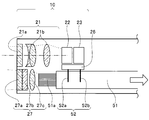
また、図3に示すように、送信回路26からは送信側導波管接続部52が延出されている。具体的にこの送信側導波管接続部52は、2つのアンテナ、送信側導波管接続アンテナ52a、52bにより構成され、これら送信側導波管接続アンテナ52a、52bは、導波管51における前記一端部近傍において前記誘電体層内(すなわち、光ファイバ51a内)に延出して配設されるようになっている(なお、詳しくは後述する)。
ここで、送信側導波管接続アンテナ52a、52bは、第1の実施形態における前記第2の接続構造104に相当する構成の一部を構成する。
なお、本第2の実施形態においても、第1の実施形態同様に、光源装置4における光源41から発生された「照明光」を、前記導波管51を有する伝送路(このとき、照明光の伝送路といえる)を経由して照明光学系27に向けて伝送するようになっている(図2における「照明光の経路(S2)」参照)。
なお、本第2の実施形態において照明光学系27は、例えば、図5に示すように、先端硬性部10の先端面に配設されたカバーガラス27aと、当該カバーガラス27aの基端側に配設され、ミリ波(およびサブミリ波)を透過させないミリ波非透過カバーガラス27bとを有する。そしてこのミリ波非透過カバーガラス27bの基端側に照明用レンズ27cが配設され、この照明用レンズ27cの基端側に光ファイバ51aの先端面が接続されるようになっている。
一方、本第2の実施形態においても、撮像ユニット20における撮像素子22において撮像した被検物の像に係る「画像信号」を、送信回路26、送信側導波管接続部52を介して前記導波管51を有する伝送路(このとき、画像情報の伝送路といえる)を経由して画像信号処理回路31Aに向けて伝送するようになっている(図2、図3における「画像情報の経路(S1)」)。
より具体的には、送信回路26から延出された前記送信側導波管接続アンテナ52a、52bにおいて、撮像素子22から出力された「画像信号」が、ミリ波またはサブミリ波の電波として当該導波管51内に送波される。そして、導波管51内に送波された画像信号は、当該導波管51内をミリ波またはサブミリ波の電波として伝搬されるようになっている。
そして、接続部11が光源装置4(およびビデオプロセッサ3)に接続された際、当該画像信号は、中継回路71から延出された受信側導波管接続アンテナ72a、72bにおいて受波された後、当該中継回路71に接続された送受信アンテナ73から再び、ミリ波またはサブミリ波の電波として送波される。
その後、当該画像信号は、受信回路33に接続された送受信アンテナ34において受波され、当該受信回路33から画像信号処理回路31Aに向けて伝送されるようになっている。
次に、本実施形態の内視鏡システムを特徴づける導波路(導波管)、並びに送信側導波管接続アンテナおよび受信側導波管接続アンテナについて詳しく説明する。
<導波管の構成について>
上述したように、本発明は、内視鏡における撮像部とビデオプロセッサにおける画像処理部とを結ぶ信号伝送方式として従来用いられてきた、リードワイヤによる信号伝送方式および光ファイバによる信号伝送方式に代わり、ミリ波またはサブミリ波(おおよそ30~600GHzの周波数を有する電波)を通す導波路(導波管)による信号伝送方式を新たに提案するものである。
上述したように、本発明は、内視鏡における撮像部とビデオプロセッサにおける画像処理部とを結ぶ信号伝送方式として従来用いられてきた、リードワイヤによる信号伝送方式および光ファイバによる信号伝送方式に代わり、ミリ波またはサブミリ波(おおよそ30~600GHzの周波数を有する電波)を通す導波路(導波管)による信号伝送方式を新たに提案するものである。
なお、本実施形態においてミリ波、サブミリ波は、ミリからサブミリオーダ(0.5~10mm程度)の波長をもつ電波を指すものとする。
本実施形態において前記導波管51は、図7に示すように、長手方向に誘電率が均一になるように延出された複数の光ファイバ51aを有する誘電体層と、長手方向に連続的に延出され前記誘電体である光ファイバ51aの外周を覆う金属層55と、当該金属層55の外側に、断面の長径と短径とが1以外の所定の比率を有する被覆部材54と、を有する。
また、導波管51は、前記被覆部材54によって前記金属層55の断面形状を長手方向に同一化するとともに、伝送される前記電波の管内波長をλgとしたとき、前記誘電体層を構成する前記光ファイバ51aの断面径は、λg/50未満に設定されるようになっている。
そして、図3、図6に示すように、一端部が前記照明光学系27に接続される一方で他端部は前記光源装置4に接続されるようになっている。
このように、本実施形態において前記導波管51は、ミリ波またはサブミリ波の電波に変換された「画像信号」を伝搬する導波路として機能する一方で、導波管51内に配設された光ファイバ51aは、いわゆる照明光を伝送するライトガイドしての役目を果たす。このとき、当該光ファイバ51aは、導波管内の内部誘電体としての役目を果たすことになる。
因みに、本実施形態において、「誘電率が均一」とは、導波管内部を伝搬する電波(ミリ波またはサブミリ波)の波長オーダーの寸法でみたときに均一であることを意味するものである。すなわち、波長オーダーよりも1~2桁以上寸法の異なる構造による誘電率分布は、導波管内部を伝搬する電波には影響を与えないため、本実施形態においては、これを含めて誘電率が均一と表現している。
また、本実施形態の導波管51における前記内部誘電体である光ファイバ51aの要件の1つとしては、その誘電損失(誘電正接tanδとして現される)が十分小さいことが挙げられる。具体的には誘電正接tanδは、10-3以下であることが望ましい。
ここで、内部誘電体における誘電損失(誘電正接tanδ)が10-3より小さい値であることの臨界的意味を説明する。より具体的には、「比誘電率εrの平方根と誘電正接tanδの積が2×10⁻³より小さいこと」の臨界的意味について説明する。
すでに述べたように、本発明はミリ波およびサブミリ波への適用が可能であり、伝送線路としての太さでいえばφ6mm以下であれば効果を持ち得るが、本発明に際して、本発明者らは本発明時点の技術状況を詳細に検討した結果として、内視鏡の内部通信で利用価値の高い導波管の要件として、以下の条件を最初に抽出した。
(1)その外形がφ2mm以下であること
(2)1mあたりの伝送損失が20dBを超えないこと
ここで、条件(1)は、当該導波管を内視鏡に内蔵するための物理的な制約条件であり、本発明時点の内視鏡製品の構成から導出している。ここで、前述のとおり内視鏡の挿入部およびユニバーサルコードはその目的から10mm程度以下の外形寸法を持つことが多い。
(2)1mあたりの伝送損失が20dBを超えないこと
ここで、条件(1)は、当該導波管を内視鏡に内蔵するための物理的な制約条件であり、本発明時点の内視鏡製品の構成から導出している。ここで、前述のとおり内視鏡の挿入部およびユニバーサルコードはその目的から10mm程度以下の外形寸法を持つことが多い。
すなわち、挿入部およびユニバーサルコードの内部には、湾曲部9(図1参照)の湾曲を実現するためのワイヤー等の内部構造、対物レンズを洗浄するための送気送水チャンネルおよび観察部の処置をするための鉗子等の処置具を挿通する鉗子チャンネルなど多くの内蔵物が含まれていることを考慮し、条件(1)として、本発明時点において伝送線路に許容される可能性の高い数値を具体的に設定した。
同様に条件(2)は、本発明時点の送受信回路の能力による制約(十分に低いビットエラーレート(誤り率)を得るには伝送損失が20dB以下程度である必要があること)と内視鏡で利用可能性のある最低の長さ(約1m)とを勘案して設定している。
また、本発明時点における無線電波技術の開発状況を鑑みると、次世代無線通信の国際規格としてIEEE802.11adが立ち上がるなど、ミリ波帯電波の中でも60GHzの利用がし易い環境が整ってきている(無線通信チップが安価に供給される見込みが立つなど、実用化を考慮したときに最も利用し易いミリ波電波の周波数が60Hzである)。
すなわち、これら周辺技術の状況を勘案し、ミリ波電波を伝搬する導波管を内視鏡内部の通信に適用するという前提においては、ミリ波電波の中でも60GHzで利用できる導波管技術を探求することが、実用化への近道だと判断した。
なお、本発明時点においては、300GHzまで一般機器にて利用可能とする為の技術開発が進んでおり、近い将来において300GHzまで利用可能となる可能性がある。この段階に至れば周波数を上げることに拠ってさらに細い導波管を利用できるようになるが、この段階に至っても本発明はその価値を失うものではなく、広く利用できるものであると確信する。
上述したこれら要件を考察し、鋭意研究を重ねた結果、本発明者は、周波数60GHzにおいて外径太さφ2以下を実現するには、導波管の内部に誘電体を配することで電磁波の波長短縮効果(電磁波は比誘電率εrの媒質内において、その波長fがεrの平方根に反比例して小さくなる)を得ることが有効であると見出した。
加えて、同試作を重ねた結果として、導波管の内部に誘電体を配した場合の伝送損失は前記誘電体の誘電損失(誘電体による損失)が支配的であることを見出した。更に理論的検討からその損失量は「比誘電率εrの平方根と誘電正接tanδの積」に大きく依存することを見出した。
さらに本発明者は、周波数60GHzにて長径が2mm以下程度(εr=3.8)となる楕円断面の導波管(図11参照)を仮定したうえで、電磁界シミュレータを用いた検討を行い、シミュレーション結果から、1mあたりの誘電損失が20dB程度となるのは、誘電正接tanδが1.0×10⁻³程度になるときであることが判った。
また、これを超えると誘電損失が急激に増加して利用可能性のある損失量ではなくなることも併せて判った。
すなわち、本発明者は、上記検討の結果、損失量は「比誘電率εrの平方根と、誘電正接tanδとの積」に大きく依存すること、また、上記のシミュレーション結果(比誘電率εr=3.8において誘電正接tanδが1.0×10⁻³程度を超えると利用可能な損失量(20dB/m)をこえる)ことから、内視鏡の内部通信で利用する導波管は、その内部誘電体の特性として、(εr=3.8の平方根が1.95であるから)比誘電率εrの平方根と誘電正接tanδの積が概ね2.0×10-3以下であることが必要であることを明確にした。
なお、当該事実は、長手方向に誘電率が均一になるように延出された導波管一般に通じて適用可能である。
本実施形態においては、導波管51の内部誘電体としてライトガイド用の光ファイバ51aを用いるものであるが、当該光ファイバ51aとしては、比誘電率εrの平方根と誘電正接tanδの積が概ね2.0×10⁻³以下となる材質(例えば、石英ガラス系のドープ剤を極力減らしたタイプなど)のファイバを採用した。
したがって、本実施形態の内視鏡システムに利用される導波管51の内部に用いられる内部誘電体としての光ファイバ51aは、ライトガイドしての機能を損なうことなく、導波路または導波管として高い性能(伝送効率)を持つことができる。
また、後述するように、本実施形態においては、光ファイバ51aに対する送信側導波管接続アンテナ52a、52bおよび受信側導波管接続アンテナ72a、72bの挿入によって、ライトガイドしての機能、および、導波管として高い性能(伝送効率)のいずれも損なうことが無いように設定されている。
すなわち、本第2の実施形態においても、導波管51の金属層55の内部空間における光ファイバ51aの充填率については80%未満に設定するものとする。このように十分な空間的な余裕があるため、当該導波管51は適切な可撓性を有するようになっている。
ここで、当該光ファイバ51aの充填率が80%であることから20%以上の隙間が存在するが、本実施形態においては、この隙間に送信側導波管接続アンテナ52a、52b、および受信側導波管接続アンテナ72a、72bを配設するようにしている。
前記送信側導波管接続アンテナ52a、52b、および受信側導波管接続アンテナ72a、72bが配設された部分においては、部分的に上述した空間的余裕は減じることになるが、もともとこの部分においては可撓性は要求されないため、機能上の問題が生じることは無い。
また、ライトガイドにおいて伝送される前記照明光は光ファイバ51aの内部を通ることから、当該照明光が減じることもない。
さらに、前記導波管51内部の誘電体層を構成する光ファイバ51aの断面径は伝送される電波の管内波長をλgとしたときに、λg/50よりも小さい径である必要がある。これは、光ファイバ51aの断面径がこれよりも大きいと、導波管51内部を伝送する電波に影響し、ミリ波電波の伝送損失を増加させてしまう虞があるためである。
この点に鑑み本実施形態においては、金属層55の外側に、断面の長径と短径とが1以外の所定の比率を有する被覆部材54を配設し、当該被覆部材54によって金属層55の断面形状を長手方向に同一化するとともに、本実施形態で利用を前提とする60GHzのミリ波電波の管内波長λgが5mm強程度であることから、誘電体層を構成する光ファイバ51aの断面径を80μmとして、λg/50未満に設定した。
因みに、光ファイバの外径は125μm以上のものが一般的であり、本実施形態ではこれよりも細い光ファイバをあえて採用している。
<送信側導波管接続アンテナおよび受信側導波管接続アンテナについて>
次に、送信側導波管接続部52(送信側導波管接続アンテナ52a、52b)および受信側導波管接続部72(受信側導波管接続アンテナ72a、72b)の構成について説明する。
次に、送信側導波管接続部52(送信側導波管接続アンテナ52a、52b)および受信側導波管接続部72(受信側導波管接続アンテナ72a、72b)の構成について説明する。
図3、図5、図6等に示すように、送信側導波管接続部52を構成する送信側導波管接続アンテナ52a、52b、および、受信側導波管接続部72を構成する受信側導波管接続アンテナ72a、72bは、いずれも、いわゆるモノポールアンテナの如き棒形状を呈し、それぞれ送信回路26、中継回路71から延出される。
また、送信側導波管接続アンテナ52a、52bおよび受信側導波管接続アンテナ72a、72bは、それぞれ送信回路26、中継回路71から延出された後、いずれも導波管51内の前記光ファイバ51aにおける上記「隙間」に挿入するように配設されている。
そして、送信側導波管接続アンテナ52a、52bは、送信回路26においてミリ波(またはサブミリ波)に変換された「画像信号」を導波管51内に向けて送波する。また、受信側導波管接続アンテナ72a、72bは、導波管51内を伝搬するミリ波(またはサブミリ波)の「画像信号」を受波し、中継回路71に伝送する。
なお、中継回路71に伝送されたミリ波(またはサブミリ波)の「画像信号」は、上述したように、接続部11が光源装置4に接続された際において(図6に示す状態)、当該中継回路71から送受信アンテナ73を介して再度ミリ波(またはサブミリ波)の電波として送波されるようになっている。
図6に示すように、中継回路71から送波されたミリ波(またはサブミリ波)の電波は、極めて近距離を伝搬し、受信回路33に接続せれた送受信アンテナ34(図6においては図示せず)において受波し、受信回路33に伝送されるようになっている。
これら送信側導波管接続アンテナ52a、52bおよび受信側導波管接続アンテナ72a、72bは、いずれも、信号を含むミリ波(またはサブミリ波)を効率よく送波するために(または受波するために)、長さを含む形状は適切に設計されるようになっている。すなわち、送信回路26、または中継回路71(または受信回路33)内部の特性インピーダンスと導波管51内部の特性インピーダンスとが整合するように長さを含む形状が適切に設計されるようになっている。
ここで、本第2の実施形態におけるこれら送信側導波管接続アンテナ52a、52bおよび受信側導波管接続アンテナ72a、72bの接続形態について考察する。
図8は、従来の、一般の同軸導波管変換機構における接続形態の一例を示した説明図である。
一般に導波管に送受信用アンテナを導入して接続する場合、図8に示す如き接続形態を呈する(図中、“同軸線”は送受信用アンテナを示す)。
なお、この種の同軸導波管変換機構における接続形態は広く知られるところにあり、例えば、日本国特許第5697779号明細書、日本国特開2016-111459号公報、日本国特開2015-103886号公報、日本国特許第4764358号明細書等に詳しい。
図8に戻って、係る従来の同軸導波管変換機構における接続形態においては、導波管の一方向が閉じていることから、アンテナから発せられた電波は、導波管の開口がわの方向にのみ伝達することとなる。これは、通常は、電波を的確に伝搬するためにも至極当然の構成といえる。
なお、この図8に示す従来の形態であっても、効率の良い伝達を実現するためにアンテナの形状等を最適化する必要があるのはいうまでもない。
ところで、図8に示す形態では、導波管の一方向(図8中、向かって左側)が閉じていることから、当該閉方向に向けて電波および光を伝搬させることはできない。
本発明は、導波管51内の内部誘電体としてライトガイド用の光ファイバ51aを用いることから、当然に、ライトガイドとしての機能も果たさざるを得ない。すなわち、図8でいえば、図中向かって左側の閉じている方向に「照明光」を伝達する必要がある。
係る点に鑑みるに、本発明の如き「画像信号」の伝送路として上述の如き導波管51を採用する構成においては、図8に示す如き従来の接続形態を採用することは不可能であるといえる。
本発明は、上述した点にも鑑みてなされており、導波管51内の内部誘電体としてライトガイド用の光ファイバ51aを用いる構成を採用しながら、通常の内視鏡システムと同様に照明光の伝達を妨げることなく、撮像素子22が撮像した被写体像に係る画像信号をミリ波(またはサブミリ波)の電波として導波管51を適切に伝搬可能とする内視鏡システムを提供するものである。
図9は、第2の実施の形態にかかる内視鏡システムに採用する同軸導波管変換機構の概念を示した説明図であり、図10は、第2の実施の形態にかかる内視鏡システムにおける同軸導波管変換機構の具体例を示した説明図である。
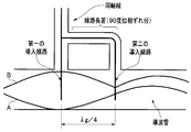
図9に示すように、本第2の実施形態における同軸導波管変換機構の概念としては、まず、第1の送受信用アンテナ(図中、第1の導入線路)を導波管に導入して接続する。そして、この第1の送受信用アンテナから第2の送受信用アンテナ(図中、第2の導入線路)を分岐し、この第2の送受信用アンテナを前記第1の送受信用アンテナに対して、伝送路(導波管)の長手方向に1/4波長分(λg/4)ほど離間させた位置において導波管に導入して接続する。
さらに、第1の送受信用アンテナと第2の送受信用アンテナとは、一方のアンテナから送信される信号の位相と他方の前記アンテナから送信される信号の位相とが90度ずれるように設定する。
このように設定される第1の送受信用アンテナおよび第2の送受信用アンテナの作用について、図9を参照して説明する。
図9において、位相曲線Aは、第1の導入線路から導波管の内部に導入される電波を示し、位相曲線Bは、第2の導入線路から導入される電波である。ここで、曲線Bは曲線Aに比べて、位相が90度遅れているため、図9中、向かって右方向に進行する波は、AとBとで位相が揃い、強めあう干渉状態が作られる。同様に図9中、向かって左方向に進行する波は、AとBとで位相が逆になり、弱めあう干渉となる。
この結果、導波管に供給される波は図9中、向かって右方向だけとなり、導入線路(同軸線)と導波管とで効率のよい接続が可能となる。
次に、本第2の実施形態における同軸導波管変換機構の具体例について図10を参照して説明する。なお、ここでは、代表して送信側導波管接続アンテナ52a、52bを例にして説明する。
図10に示すように、本第2の実施形態における同軸導波管変換機構においては、まず、送信回路26の内部において、送信側導波管接続アンテナ52aに対して送信側導波管接続アンテナ52bが分岐される(図中、符号26a参照)。そして、送信側導波管接続アンテナ52aと、送信側導波管接続アンテナ52bとが、伝送路(導波管)の長手方向に、互いに1/4波長分(λg/4)ほど離間して配置されるようになっている。
また、本第2の実施形態において、送信側導波管接続アンテナ52aと送信側導波管接続アンテナ52bとは、2本のアンテナのうちの一方のアンテナから送信される信号の位相と、他方のアンテナから送信される信号の位相とが互いに90度ずれて配置されるようになっている。
図10に示すように、本第2の実施形態の内視鏡システムにおいては、上記同様に、曲線Bは曲線Aに比べて位相が90度遅れているため、図10中、導波管51を向かって右方向に進行する波は、曲線Aと曲線Bとで位相が揃い、強めあう干渉状態が作られる。同様に図10中、向かって左方向に進行する波は、曲線Aと曲線Bとで位相が逆になり、弱めあう干渉となる。
この結果、本第2の実施形態の内視鏡システムにおいては、導波管51に供給される波は、図10中、向かって右方向だけとなり、導入線路(同軸線)と導波管51とで効率のよい接続が可能となる。
なお、上述した例においては、代表して送信側導波管接続アンテナ52a、52bを例にして説明したが、本第2の実施形態においては、受信側導波管接続アンテナ72a、72bについても同様に構成され、同様の効果を奏すものである。
(作用)
次に、上述した如き構成をなす本第2の実施形態の内視鏡システムにおける作用について説明する。
次に、上述した如き構成をなす本第2の実施形態の内視鏡システムにおける作用について説明する。
撮像素子22は、撮像光学系21に入光された被写体像を撮像素子面において受光し電気信号に光電変換してアナログの撮像信号として出力する。
その後ドライバIC23は、内部のAFE24において、撮像素子22から出力されたアナログの撮像信号に対してA/D変換等の所定の処理を施しデジタルの画像信号として出力する。なお、このとき図示しないパラレル/シリアル変換部においてシリアルのデジタル信号に変換される。
さらにドライバIC23に接続される送信回路26は、ミリ波・サブミリ波の搬送波を前記画像信号により変調し、送信側導波管接続アンテナ52a、52bから当該画像情報が載ったミリ波・サブミリ波の電波として導波路(導波管)51に向けて送信する。
その後、送信側導波管接続アンテナ52a、52bから送波されたミリ波・サブミリ波の電波は、導波管51を通じてビデオプロセッサ3における画像信号処理回路31Aに送られる。
すなわち、導波管51内の光ファイバ51aに挿入配置された送信側導波管接続アンテナ52a、52bから送波されたミリ波(またはサブミリ波)の電波は、導波管51内を伝搬し、光ファイバ51aに挿入配置された受信側導波管接続アンテナ72a、72bにうおいて受波される。
そして、受信側導波管接続アンテナ72a、72bにおいて受波されたミリ波(またはサブミリ波)の電波は、中継回路71において再び変調され、送受信アンテナ73から送波される。
前記中継回路71(送受信アンテナ73)から送波されたミリ波(またはサブミリ波)の電波は、送受信アンテナ34において受信され、受信回路33において、所定の画像情報が取り出され、その後、受信回路33からビデオプロセッサ3における画像信号処理回路31Aに伝送される。
そして、受信回路33において取り出された画像情報は画像信号処理回路31Aにおいて適宜画像処理が施され、前記表示装置5に投影される。
一方、光源装置4における光源41からは所定の照明光が発せされ、当該照明光は、導波管51内に内部誘電体として配設された光ファイバ51a内を伝送される。そして、ライトガイドの機能を有する当該光ファイバ51aを伝送する照明光は、照明光学系27から被写体に向けて照射される。
(効果)
以上説明したように、本第2の実施形態の内視鏡システムは、第1の実施形態と同様に、リードワイヤによる信号伝送方式の課題である伝送速度の限界を克服しつつ、光ファイバによる信号伝送方式の課題をも克服する新しい信号伝送方式を備える内視鏡システムを提供することができる。
以上説明したように、本第2の実施形態の内視鏡システムは、第1の実施形態と同様に、リードワイヤによる信号伝送方式の課題である伝送速度の限界を克服しつつ、光ファイバによる信号伝送方式の課題をも克服する新しい信号伝送方式を備える内視鏡システムを提供することができる。
また、本第2の実施形態においては、導波管51内の内部誘電体としてライトガイド用の光ファイバ51aを用いる構成を採用しながら、通常の内視鏡システムと同様に照明光の伝達を妨げることなく、撮像素子22が撮像した被写体像に係る画像信号をミリ波(またはサブミリ波)の電波として導波管51を適切に伝搬可能とする内視鏡システムを提供することができる。
なお、上述した第1、第2の実施形態においては、撮像素子22からの画像情報を処理し信号伝送を行なうドライバIC23は、上述したようにアナログフロントエンド、タイミングジェネレータ、送受信回路が全てシリコンCMOSプロセスにより作成され、十分に小型化されている。
この中でも、送信回路26および受信回路33はモノシリックマイクロ波集積回路(MMIC)により構成されることから回路の小型化に寄与している。
このようにドライバIC23の小型化を実現した結果、フルハイビジョン画像信号の高い信頼性での伝送と、先端部の小型化を両立することを可能としている。
さらに、導波管の利用により、撮像ユニット側アンテナから発せられた電波は、導波管内に閉じ込められる形で伝播するため、拡散などによるロスが最小に抑えられる。すなわち、送信に必要な電力量の最小化をも果たすことができている。
また、本実施形態の効果について、従来技術である日本国特開昭61-121590号公報、および日本国特許第3748979号明細書に記載の技術と対比させて説明する。
上述したように、本実施形態の内視鏡システムにおいては、導波管51を伝送される前記ミリ波・サブミリ波は、ミリからサブミリオーダの波長を有する電波であって概略で30~600GHzの周波数を有することから、上述した日本国特開昭61-121590号公報に記載のリードワイヤ方式における伝送速度の問題については解決することができる。すなわち、2.5Gbps以上の信号伝送速度を問題なく実現することができる。
また、ミリ波・サブミリ波においては、通常の電波通信で実績のある多様な信号変調方式を利用しやすく、情報伝送の密度を高めやすいという利点を持つことから、機器の構成によっては、上述した日本国特許第3748979号明細書に記載する光ファイバによる光信号伝送方式よりも情報速度を高めることが可能となる。
また、伝送信号であるミリ波・サブミリ波を伝送効率の良い導波路に閉じ込めて伝送するために、十分な信号強度を得られるうえに、伝送が途中で不安定になるような心配がない。
また、老朽化に伴い、仮に導波路が劣化し、内部に配された光ファイバが徐々に断裂し、または、亀裂等により導波路が切断することがあっても、ミリ波・サブミリ波は前記断裂部または切断部を含めて伝播するうえに、上述した理由により、本実施形態においては信号伝送路(導波路)を十分に太くすることができるために、信号伝送の品質は劣化することはあっても、信号伝送自体が突然途切れることは無い。
因みに、上述した日本国特許第3748979号明細書に記載する光ファイバは、通信用の光ファイバのようにエラストマー樹脂等の部材により光ファイバ線に保護することが難しく、繰り返しの曲げや外部からの衝撃により破断し、通信が突然途切れる虞がある。
すなわち、日本国特許第3748979号明細書に記載する技術と本実施形態とでは、通信の信頼性は、明確に本実施形態が勝る。
なお、通信用の光ファイバを用いた通信形態は広く提案が為されており、例えば、日本国特開2007-260066号公報、日本国特開2010-194037号公報等において詳しい。この形態において通信に用いる光ファイバ線は通常、上述のとおりエラストマー樹脂等で外側が保護されており、繰り返し曲げ程度破談することはほとんど無いが、この場合も意図しない程に強い衝撃等を受けた場合においては断線することが無いとまではいえない。すなわち、通信の信頼性の観点でいえば、本実施形態は、通信用の光ファイバを用いた通信形態に対しても優位性をもつといえる。
また、上述したように、本実施形態においては、撮像素子22として、200万画素以上のいわゆるフルハイビジョン相当以上の画素数を持つ固体撮像素子を採用したが、本実施形態は、上述したように2.5Gbps以上の信号伝送速度を可能とするため、斯様な画素数であっても支障はない。
さらに、本実施形態の内視鏡システムは、湾曲部、可撓管部を備える挿入部6を構成要素とする内視鏡2を有し、すなわち、屈曲部を有することで先端硬性部の方向を自在に変更し所望の方向の画像を取得する機能を持つビデオ内視鏡システムにおいても、日本国特開昭61-121590号公報および日本国特許第3748979号明細書に記載する技術に関する課題を解決した上で、先端部の小さいビデオ内視鏡システムを実現できる。
これは、ミリ波・サブミリ波によれば小さい通信回路を実現できるということだけでなく、ミリ波・サブミリ波によれば撮像ユニットの外から、電源となるエネルギーや動作クロックを撮像ユニットに送ることが可能であることに起因する。
すなわち、日本国特許第3748979号明細書に示すような光ファイバによる信号伝送方式では実現が困難な、フルハイビジョン画像信号の伝送と、先端部の小型化を両立することができる。
上述したように、このタイプのビデオ内視鏡システムにおいて先端部(屈曲しない部分)を小さくすることには強いニーズがあり、実際に狭い空間における観察を自由にするなど内視鏡の機能向上に大きく寄与することができる。
なお、本実施形態の内視鏡システムは、上部消化管のビデオ内視鏡システムであることを前提としたが、撮像ユニットが先端部に配された挿入部と、前記撮像ユニットにおいて生成された画像信号を処理する画像処理部と、前記撮像ユニットと前記画像処理部とを結ぶ信号伝送路を有するビデオ内視鏡システムであれば、内視鏡の種類に拠らず上記同様の効果を得ることができる。
すなわち、下部消化管(大腸)用内視鏡など各種の消化管用内視鏡はもちろんのこと、内視鏡外科手術において用いられる各種外科用内視鏡、パイプ、機械、各種構造物の内部を観察するための各種工業用内視鏡などにおいて、それぞれ同様の効果を得ることができる。
また本実施形態においては、上述したように、撮像ユニット20の構成として、撮像素子22、ドライバIC23、送信回路26および図示しないコンデンサを含み、前記ドライバIC23はアナログフロントエンド(AFE)24、タイミングジェネレータ(TG)25および図示しない制御部を備えるものとしたが、この構成はこれに限らずとも、同様の効果を得ることができる。
たとえば、ドライバIC23内にあるアナログフロントエンド(AFE)24、タイミングジェネレータ(TG)25は、撮像素子22内に含めることも可能であり、この場合も同様の効果を得ることができる。
また内視鏡2側における送信回路26およびビデオプロセッサ3側における受信回路33は、いずれもモノシリックマイクロは集積回路(MMIC)として、上述したように回路の小型化において最適な構成としたが、これに拠らずとも、フルハイビジョン画像信号の高い信頼性での伝送は可能であり、同様の効果を得ることはできる。
本発明は、上述した実施形態に限定されるものではなく、本発明の要旨を変えない範囲において、種々の変更、改変等が可能である。
本出願は、2016年11月28日に日本国に出願された特願2016-230251号を優先権主張の基礎として出願するものであり、上記の開示内容は、本願明細書、請求の範囲に引用されるものとする。
Claims (5)
- 被検物に照射するための照明光を発生させる光源装置と、画像信号に対して所定の画像処理を施す画像処理部と、を有する第1ユニットと、
前記光源装置からの前記照明光を受けて前記被検物に照射する照明光学系と、前記被検物を撮像して前記画像信号を生成する撮像部と、を有する第2ユニットと、
前記第1ユニットと前記第2ユニットとの間に設けられ、ミリ波またはサブミリ波を伝搬する導波路であって両端が解放された導波管を有する伝送路と、
を備え、
前記伝送路における前記導波管は、長手方向に誘電率が均一になるように延出された複数の光ファイバを有する誘電体層と、長手方向に連続的に延出され前記誘電体層の外周を覆う金属層と、を有し、一端部が前記照明光学系に接続される一方で他端部は前記光源装置に接続され、
前記第1ユニットは、前記画像信号を受信する受信回路をさらに有すると共に、前記導波管における前記他端部において前記誘電体層内に延出して配設され、当該受信回路と前記伝送路との第1接続部を形成する第1の接続構造を有し、
前記第2ユニットは、前記画像信号を送信する送信回路をさらに有すると共に、前記導波管における前記一端部において前記誘電体層内に延出して配設され、当該送信回路と前記伝送路との第2接続部を形成する第2の接続構造を有する
ことを特徴とする撮像装置。 - 前記撮像装置は内視鏡装置であって、
前記撮像部は、200万画素以上の固体撮像素子を有し、前記送信回路は、前記画像信号をミリ波またはサブミリ波の電波にて送信し、前記誘電体層は、伝送される当該電波の周波数における誘電損失tanδが10-3より小さい値である
ことを特徴とする請求項1に記載の撮像装置。 - 前記伝送路の少なくとも一部が可撓性を有し、前記伝送路における当該可撓性を有する部分において、前記金属層の内部空間における前記光ファイバの充填率が80%未満である
ことを特徴とする請求項2に記載の撮像装置。 - 前記金属層の外側に、断面の長径と短径とが1以外の所定の比率を有する被覆部材を有し、前記被覆部材によって前記金属層の断面形状を長手方向に同一化するとともに、伝送される前記電波の管内波長をλgとしたとき、前記誘電体層を構成する前記光ファイバの断面径は、λg/50未満である
ことを特徴とする請求項2に記載の撮像装置。 - 前記第1の接続構造および前記第2の接続構造は、いずれも2本のアンテナにより構成され、前記2本のアンテナは、前記伝送路の長手方向に1/4波長分離間して配置されるとともに、一方の前記アンテナから送信される信号の位相と他方の前記アンテナから送信される信号の位相とが90度ずれている
ことを特徴とする請求項1に記載の撮像装置。
Applications Claiming Priority (2)
| Application Number | Priority Date | Filing Date | Title |
|---|---|---|---|
| JP2016-230251 | 2016-11-28 | ||
| JP2016230251A JP2018086067A (ja) | 2016-11-28 | 2016-11-28 | 撮像装置 |
Publications (1)
| Publication Number | Publication Date |
|---|---|
| WO2018096822A1 true WO2018096822A1 (ja) | 2018-05-31 |
Family
ID=62195859
Family Applications (1)
| Application Number | Title | Priority Date | Filing Date |
|---|---|---|---|
| PCT/JP2017/036928 Ceased WO2018096822A1 (ja) | 2016-11-28 | 2017-10-12 | 撮像装置 |
Country Status (2)
| Country | Link |
|---|---|
| JP (1) | JP2018086067A (ja) |
| WO (1) | WO2018096822A1 (ja) |
Families Citing this family (1)
| Publication number | Priority date | Publication date | Assignee | Title |
|---|---|---|---|---|
| JP7143229B2 (ja) * | 2019-01-10 | 2022-09-28 | オリンパス株式会社 | 電気コネクタ、複合コネクタ及び内視鏡 |
Citations (3)
| Publication number | Priority date | Publication date | Assignee | Title |
|---|---|---|---|---|
| WO2013096584A2 (en) * | 2011-12-20 | 2013-06-27 | Old Dominion University Research Foundation | Electromanipulation of cells and other biologicaltissues by pulsed electric fields at elevated temperatures |
| JP2013162149A (ja) * | 2012-02-01 | 2013-08-19 | Sony Corp | 伝送方法、及び、伝送システム |
| JP2015186556A (ja) * | 2014-03-27 | 2015-10-29 | 富士フイルム株式会社 | 内視鏡装置及びその制御方法 |
Family Cites Families (3)
| Publication number | Priority date | Publication date | Assignee | Title |
|---|---|---|---|---|
| JP3748979B2 (ja) * | 1997-04-23 | 2006-02-22 | オリンパス株式会社 | 電子内視鏡装置 |
| JP2003115707A (ja) * | 2001-10-05 | 2003-04-18 | Kuraray Co Ltd | 表面波伝送線路 |
| JP4724849B2 (ja) * | 2006-07-19 | 2011-07-13 | 福井県 | 誘電体ケーブルおよび導波管 |
-
2016
- 2016-11-28 JP JP2016230251A patent/JP2018086067A/ja active Pending
-
2017
- 2017-10-12 WO PCT/JP2017/036928 patent/WO2018096822A1/ja not_active Ceased
Patent Citations (3)
| Publication number | Priority date | Publication date | Assignee | Title |
|---|---|---|---|---|
| WO2013096584A2 (en) * | 2011-12-20 | 2013-06-27 | Old Dominion University Research Foundation | Electromanipulation of cells and other biologicaltissues by pulsed electric fields at elevated temperatures |
| JP2013162149A (ja) * | 2012-02-01 | 2013-08-19 | Sony Corp | 伝送方法、及び、伝送システム |
| JP2015186556A (ja) * | 2014-03-27 | 2015-10-29 | 富士フイルム株式会社 | 内視鏡装置及びその制御方法 |
Also Published As
| Publication number | Publication date |
|---|---|
| JP2018086067A (ja) | 2018-06-07 |
Similar Documents
| Publication | Publication Date | Title |
|---|---|---|
| JP6724001B2 (ja) | 内視鏡システム | |
| US9247867B2 (en) | Endoscopic arrangement | |
| JP4841391B2 (ja) | 内視鏡 | |
| US8690759B2 (en) | Endoscopic instrument | |
| JP5038059B2 (ja) | 電子内視鏡及び内視鏡装置 | |
| EP2624304B1 (en) | Optical transmission module, image capturing device, and endoscope | |
| US10090611B2 (en) | Cable, cable connection structure, and imaging apparatus | |
| JP5861071B1 (ja) | 内視鏡 | |
| JP2008142410A (ja) | 被検体内導入装置 | |
| CN101587239A (zh) | 电子内窥镜装置 | |
| CN102549846B (zh) | 安装构造体及集合线缆 | |
| WO2018116853A1 (ja) | 誘電体混合材料、誘電体混合材料を含む可撓性導波管、可撓性導波管を有する画像伝送装置、可撓性導波管を有する内視鏡、および内視鏡システム | |
| JP2011010886A (ja) | 電子内視鏡 | |
| JP6795967B2 (ja) | 導波管、導波管を有する画像伝送装置、導波管を有する内視鏡および内視鏡システム | |
| WO2018096822A1 (ja) | 撮像装置 | |
| JP2020058524A (ja) | 可撓性導波管、可撓性導波管を有する画像伝送装置、可撓性導波管を有する内視鏡および内視鏡システム | |
| US8723921B2 (en) | Image pickup system | |
| JP2021166565A (ja) | 内視鏡システム | |
| WO2018096803A1 (ja) | 内視鏡システム | |
| JP2011200338A (ja) | 電子内視鏡 | |
| JP7143229B2 (ja) | 電気コネクタ、複合コネクタ及び内視鏡 | |
| US20230346209A1 (en) | Insertion device | |
| US20250204745A1 (en) | Endoscope apparatus | |
| JP6421985B2 (ja) | 内視鏡 | |
| KR20180087531A (ko) | 데이터의 빠른 전송을 위한 광대역 컨포멀 안테나 |
Legal Events
| Date | Code | Title | Description |
|---|---|---|---|
| 121 | Ep: the epo has been informed by wipo that ep was designated in this application |
Ref document number: 17874123 Country of ref document: EP Kind code of ref document: A1 |
|
| NENP | Non-entry into the national phase |
Ref country code: DE |
|
| 122 | Ep: pct application non-entry in european phase |
Ref document number: 17874123 Country of ref document: EP Kind code of ref document: A1 |