WO2018096734A1 - Semiconductor module - Google Patents
Semiconductor module Download PDFInfo
- Publication number
- WO2018096734A1 WO2018096734A1 PCT/JP2017/028626 JP2017028626W WO2018096734A1 WO 2018096734 A1 WO2018096734 A1 WO 2018096734A1 JP 2017028626 W JP2017028626 W JP 2017028626W WO 2018096734 A1 WO2018096734 A1 WO 2018096734A1
- Authority
- WO
- WIPO (PCT)
- Prior art keywords
- electrode pad
- transistor
- wiring pattern
- main electrode
- electrically connected
- Prior art date
Links
- 239000004065 semiconductor Substances 0.000 title claims abstract description 71
- 238000010521 absorption reaction Methods 0.000 claims abstract description 8
- 239000000758 substrate Substances 0.000 claims description 25
- 230000000149 penetrating effect Effects 0.000 claims description 2
- 238000006243 chemical reaction Methods 0.000 description 13
- 239000013256 coordination polymer Substances 0.000 description 11
- 239000003990 capacitor Substances 0.000 description 9
- 239000000463 material Substances 0.000 description 9
- RYGMFSIKBFXOCR-UHFFFAOYSA-N Copper Chemical compound [Cu] RYGMFSIKBFXOCR-UHFFFAOYSA-N 0.000 description 8
- 229910052802 copper Inorganic materials 0.000 description 8
- 239000010949 copper Substances 0.000 description 8
- 239000004020 conductor Substances 0.000 description 6
- 238000010586 diagram Methods 0.000 description 6
- 229910000679 solder Inorganic materials 0.000 description 5
- 238000005516 engineering process Methods 0.000 description 3
- 238000009429 electrical wiring Methods 0.000 description 2
- 238000004519 manufacturing process Methods 0.000 description 2
- 238000000034 method Methods 0.000 description 2
- 230000004048 modification Effects 0.000 description 2
- 238000012986 modification Methods 0.000 description 2
- 229910052782 aluminium Inorganic materials 0.000 description 1
- XAGFODPZIPBFFR-UHFFFAOYSA-N aluminium Chemical compound [Al] XAGFODPZIPBFFR-UHFFFAOYSA-N 0.000 description 1
- PNEYBMLMFCGWSK-UHFFFAOYSA-N aluminium oxide Inorganic materials [O-2].[O-2].[O-2].[Al+3].[Al+3] PNEYBMLMFCGWSK-UHFFFAOYSA-N 0.000 description 1
- 239000000919 ceramic Substances 0.000 description 1
- 239000003985 ceramic capacitor Substances 0.000 description 1
- 229910052593 corundum Inorganic materials 0.000 description 1
- 230000006866 deterioration Effects 0.000 description 1
- 230000005669 field effect Effects 0.000 description 1
- 230000017525 heat dissipation Effects 0.000 description 1
- 229910052751 metal Inorganic materials 0.000 description 1
- 239000002184 metal Substances 0.000 description 1
- 229920001296 polysiloxane Polymers 0.000 description 1
- 239000011347 resin Substances 0.000 description 1
- 229920005989 resin Polymers 0.000 description 1
- 229910001845 yogo sapphire Inorganic materials 0.000 description 1
Images


Classifications
-
- H—ELECTRICITY
- H01—ELECTRIC ELEMENTS
- H01L—SEMICONDUCTOR DEVICES NOT COVERED BY CLASS H10
- H01L25/00—Assemblies consisting of a plurality of individual semiconductor or other solid state devices ; Multistep manufacturing processes thereof
- H01L25/16—Assemblies consisting of a plurality of individual semiconductor or other solid state devices ; Multistep manufacturing processes thereof the devices being of types provided for in two or more different main groups of groups H01L27/00 - H01L33/00, or in a single subclass of H10K, H10N, e.g. forming hybrid circuits
-
- H—ELECTRICITY
- H01—ELECTRIC ELEMENTS
- H01L—SEMICONDUCTOR DEVICES NOT COVERED BY CLASS H10
- H01L25/00—Assemblies consisting of a plurality of individual semiconductor or other solid state devices ; Multistep manufacturing processes thereof
- H01L25/03—Assemblies consisting of a plurality of individual semiconductor or other solid state devices ; Multistep manufacturing processes thereof all the devices being of a type provided for in the same subgroup of groups H01L27/00 - H01L33/00, or in a single subclass of H10K, H10N, e.g. assemblies of rectifier diodes
- H01L25/04—Assemblies consisting of a plurality of individual semiconductor or other solid state devices ; Multistep manufacturing processes thereof all the devices being of a type provided for in the same subgroup of groups H01L27/00 - H01L33/00, or in a single subclass of H10K, H10N, e.g. assemblies of rectifier diodes the devices not having separate containers
- H01L25/07—Assemblies consisting of a plurality of individual semiconductor or other solid state devices ; Multistep manufacturing processes thereof all the devices being of a type provided for in the same subgroup of groups H01L27/00 - H01L33/00, or in a single subclass of H10K, H10N, e.g. assemblies of rectifier diodes the devices not having separate containers the devices being of a type provided for in group H01L29/00
- H01L25/072—Assemblies consisting of a plurality of individual semiconductor or other solid state devices ; Multistep manufacturing processes thereof all the devices being of a type provided for in the same subgroup of groups H01L27/00 - H01L33/00, or in a single subclass of H10K, H10N, e.g. assemblies of rectifier diodes the devices not having separate containers the devices being of a type provided for in group H01L29/00 the devices being arranged next to each other
-
- H—ELECTRICITY
- H01—ELECTRIC ELEMENTS
- H01L—SEMICONDUCTOR DEVICES NOT COVERED BY CLASS H10
- H01L23/00—Details of semiconductor or other solid state devices
- H01L23/34—Arrangements for cooling, heating, ventilating or temperature compensation ; Temperature sensing arrangements
- H01L23/36—Selection of materials, or shaping, to facilitate cooling or heating, e.g. heatsinks
- H01L23/373—Cooling facilitated by selection of materials for the device or materials for thermal expansion adaptation, e.g. carbon
- H01L23/3736—Metallic materials
-
- H—ELECTRICITY
- H01—ELECTRIC ELEMENTS
- H01L—SEMICONDUCTOR DEVICES NOT COVERED BY CLASS H10
- H01L23/00—Details of semiconductor or other solid state devices
- H01L23/48—Arrangements for conducting electric current to or from the solid state body in operation, e.g. leads, terminal arrangements ; Selection of materials therefor
- H01L23/488—Arrangements for conducting electric current to or from the solid state body in operation, e.g. leads, terminal arrangements ; Selection of materials therefor consisting of soldered or bonded constructions
- H01L23/492—Bases or plates or solder therefor
-
- H—ELECTRICITY
- H01—ELECTRIC ELEMENTS
- H01L—SEMICONDUCTOR DEVICES NOT COVERED BY CLASS H10
- H01L23/00—Details of semiconductor or other solid state devices
- H01L23/48—Arrangements for conducting electric current to or from the solid state body in operation, e.g. leads, terminal arrangements ; Selection of materials therefor
- H01L23/488—Arrangements for conducting electric current to or from the solid state body in operation, e.g. leads, terminal arrangements ; Selection of materials therefor consisting of soldered or bonded constructions
- H01L23/495—Lead-frames or other flat leads
- H01L23/49517—Additional leads
- H01L23/49531—Additional leads the additional leads being a wiring board
-
- H—ELECTRICITY
- H01—ELECTRIC ELEMENTS
- H01L—SEMICONDUCTOR DEVICES NOT COVERED BY CLASS H10
- H01L23/00—Details of semiconductor or other solid state devices
- H01L23/48—Arrangements for conducting electric current to or from the solid state body in operation, e.g. leads, terminal arrangements ; Selection of materials therefor
- H01L23/488—Arrangements for conducting electric current to or from the solid state body in operation, e.g. leads, terminal arrangements ; Selection of materials therefor consisting of soldered or bonded constructions
- H01L23/495—Lead-frames or other flat leads
- H01L23/49541—Geometry of the lead-frame
- H01L23/49562—Geometry of the lead-frame for devices being provided for in H01L29/00
-
- H—ELECTRICITY
- H01—ELECTRIC ELEMENTS
- H01L—SEMICONDUCTOR DEVICES NOT COVERED BY CLASS H10
- H01L23/00—Details of semiconductor or other solid state devices
- H01L23/48—Arrangements for conducting electric current to or from the solid state body in operation, e.g. leads, terminal arrangements ; Selection of materials therefor
- H01L23/488—Arrangements for conducting electric current to or from the solid state body in operation, e.g. leads, terminal arrangements ; Selection of materials therefor consisting of soldered or bonded constructions
- H01L23/495—Lead-frames or other flat leads
- H01L23/49575—Assemblies of semiconductor devices on lead frames
-
- H—ELECTRICITY
- H01—ELECTRIC ELEMENTS
- H01L—SEMICONDUCTOR DEVICES NOT COVERED BY CLASS H10
- H01L23/00—Details of semiconductor or other solid state devices
- H01L23/48—Arrangements for conducting electric current to or from the solid state body in operation, e.g. leads, terminal arrangements ; Selection of materials therefor
- H01L23/488—Arrangements for conducting electric current to or from the solid state body in operation, e.g. leads, terminal arrangements ; Selection of materials therefor consisting of soldered or bonded constructions
- H01L23/495—Lead-frames or other flat leads
- H01L23/49589—Capacitor integral with or on the leadframe
-
- H—ELECTRICITY
- H01—ELECTRIC ELEMENTS
- H01L—SEMICONDUCTOR DEVICES NOT COVERED BY CLASS H10
- H01L23/00—Details of semiconductor or other solid state devices
- H01L23/52—Arrangements for conducting electric current within the device in operation from one component to another, i.e. interconnections, e.g. wires, lead frames
- H01L23/538—Arrangements for conducting electric current within the device in operation from one component to another, i.e. interconnections, e.g. wires, lead frames the interconnection structure between a plurality of semiconductor chips being formed on, or in, insulating substrates
- H01L23/5386—Geometry or layout of the interconnection structure
-
- H—ELECTRICITY
- H01—ELECTRIC ELEMENTS
- H01L—SEMICONDUCTOR DEVICES NOT COVERED BY CLASS H10
- H01L23/00—Details of semiconductor or other solid state devices
- H01L23/58—Structural electrical arrangements for semiconductor devices not otherwise provided for, e.g. in combination with batteries
- H01L23/62—Protection against overvoltage, e.g. fuses, shunts
-
- H—ELECTRICITY
- H01—ELECTRIC ELEMENTS
- H01L—SEMICONDUCTOR DEVICES NOT COVERED BY CLASS H10
- H01L29/00—Semiconductor devices adapted for rectifying, amplifying, oscillating or switching, or capacitors or resistors with at least one potential-jump barrier or surface barrier, e.g. PN junction depletion layer or carrier concentration layer; Details of semiconductor bodies or of electrodes thereof ; Multistep manufacturing processes therefor
- H01L29/66—Types of semiconductor device ; Multistep manufacturing processes therefor
- H01L29/68—Types of semiconductor device ; Multistep manufacturing processes therefor controllable by only the electric current supplied, or only the electric potential applied, to an electrode which does not carry the current to be rectified, amplified or switched
- H01L29/76—Unipolar devices, e.g. field effect transistors
- H01L29/772—Field effect transistors
- H01L29/78—Field effect transistors with field effect produced by an insulated gate
- H01L29/7827—Vertical transistors
-
- H—ELECTRICITY
- H02—GENERATION; CONVERSION OR DISTRIBUTION OF ELECTRIC POWER
- H02M—APPARATUS FOR CONVERSION BETWEEN AC AND AC, BETWEEN AC AND DC, OR BETWEEN DC AND DC, AND FOR USE WITH MAINS OR SIMILAR POWER SUPPLY SYSTEMS; CONVERSION OF DC OR AC INPUT POWER INTO SURGE OUTPUT POWER; CONTROL OR REGULATION THEREOF
- H02M1/00—Details of apparatus for conversion
- H02M1/32—Means for protecting converters other than automatic disconnection
- H02M1/34—Snubber circuits
-
- H—ELECTRICITY
- H02—GENERATION; CONVERSION OR DISTRIBUTION OF ELECTRIC POWER
- H02M—APPARATUS FOR CONVERSION BETWEEN AC AND AC, BETWEEN AC AND DC, OR BETWEEN DC AND DC, AND FOR USE WITH MAINS OR SIMILAR POWER SUPPLY SYSTEMS; CONVERSION OF DC OR AC INPUT POWER INTO SURGE OUTPUT POWER; CONTROL OR REGULATION THEREOF
- H02M7/00—Conversion of ac power input into dc power output; Conversion of dc power input into ac power output
- H02M7/003—Constructional details, e.g. physical layout, assembly, wiring or busbar connections
-
- H—ELECTRICITY
- H02—GENERATION; CONVERSION OR DISTRIBUTION OF ELECTRIC POWER
- H02M—APPARATUS FOR CONVERSION BETWEEN AC AND AC, BETWEEN AC AND DC, OR BETWEEN DC AND DC, AND FOR USE WITH MAINS OR SIMILAR POWER SUPPLY SYSTEMS; CONVERSION OF DC OR AC INPUT POWER INTO SURGE OUTPUT POWER; CONTROL OR REGULATION THEREOF
- H02M7/00—Conversion of ac power input into dc power output; Conversion of dc power input into ac power output
- H02M7/42—Conversion of dc power input into ac power output without possibility of reversal
- H02M7/44—Conversion of dc power input into ac power output without possibility of reversal by static converters
- H02M7/48—Conversion of dc power input into ac power output without possibility of reversal by static converters using discharge tubes with control electrode or semiconductor devices with control electrode
- H02M7/53—Conversion of dc power input into ac power output without possibility of reversal by static converters using discharge tubes with control electrode or semiconductor devices with control electrode using devices of a triode or transistor type requiring continuous application of a control signal
- H02M7/537—Conversion of dc power input into ac power output without possibility of reversal by static converters using discharge tubes with control electrode or semiconductor devices with control electrode using devices of a triode or transistor type requiring continuous application of a control signal using semiconductor devices only, e.g. single switched pulse inverters
- H02M7/538—Conversion of dc power input into ac power output without possibility of reversal by static converters using discharge tubes with control electrode or semiconductor devices with control electrode using devices of a triode or transistor type requiring continuous application of a control signal using semiconductor devices only, e.g. single switched pulse inverters in a push-pull configuration
-
- H—ELECTRICITY
- H01—ELECTRIC ELEMENTS
- H01L—SEMICONDUCTOR DEVICES NOT COVERED BY CLASS H10
- H01L2224/00—Indexing scheme for arrangements for connecting or disconnecting semiconductor or solid-state bodies and methods related thereto as covered by H01L24/00
- H01L2224/01—Means for bonding being attached to, or being formed on, the surface to be connected, e.g. chip-to-package, die-attach, "first-level" interconnects; Manufacturing methods related thereto
- H01L2224/02—Bonding areas; Manufacturing methods related thereto
- H01L2224/04—Structure, shape, material or disposition of the bonding areas prior to the connecting process
- H01L2224/06—Structure, shape, material or disposition of the bonding areas prior to the connecting process of a plurality of bonding areas
- H01L2224/0601—Structure
- H01L2224/0603—Bonding areas having different sizes, e.g. different heights or widths
-
- H—ELECTRICITY
- H01—ELECTRIC ELEMENTS
- H01L—SEMICONDUCTOR DEVICES NOT COVERED BY CLASS H10
- H01L2224/00—Indexing scheme for arrangements for connecting or disconnecting semiconductor or solid-state bodies and methods related thereto as covered by H01L24/00
- H01L2224/01—Means for bonding being attached to, or being formed on, the surface to be connected, e.g. chip-to-package, die-attach, "first-level" interconnects; Manufacturing methods related thereto
- H01L2224/42—Wire connectors; Manufacturing methods related thereto
- H01L2224/47—Structure, shape, material or disposition of the wire connectors after the connecting process
- H01L2224/49—Structure, shape, material or disposition of the wire connectors after the connecting process of a plurality of wire connectors
- H01L2224/491—Disposition
- H01L2224/4911—Disposition the connectors being bonded to at least one common bonding area, e.g. daisy chain
- H01L2224/49111—Disposition the connectors being bonded to at least one common bonding area, e.g. daisy chain the connectors connecting two common bonding areas, e.g. Litz or braid wires
-
- H—ELECTRICITY
- H02—GENERATION; CONVERSION OR DISTRIBUTION OF ELECTRIC POWER
- H02M—APPARATUS FOR CONVERSION BETWEEN AC AND AC, BETWEEN AC AND DC, OR BETWEEN DC AND DC, AND FOR USE WITH MAINS OR SIMILAR POWER SUPPLY SYSTEMS; CONVERSION OF DC OR AC INPUT POWER INTO SURGE OUTPUT POWER; CONTROL OR REGULATION THEREOF
- H02M1/00—Details of apparatus for conversion
- H02M1/32—Means for protecting converters other than automatic disconnection
- H02M1/34—Snubber circuits
- H02M1/346—Passive non-dissipative snubbers
-
- H—ELECTRICITY
- H02—GENERATION; CONVERSION OR DISTRIBUTION OF ELECTRIC POWER
- H02M—APPARATUS FOR CONVERSION BETWEEN AC AND AC, BETWEEN AC AND DC, OR BETWEEN DC AND DC, AND FOR USE WITH MAINS OR SIMILAR POWER SUPPLY SYSTEMS; CONVERSION OF DC OR AC INPUT POWER INTO SURGE OUTPUT POWER; CONTROL OR REGULATION THEREOF
- H02M1/00—Details of apparatus for conversion
- H02M1/32—Means for protecting converters other than automatic disconnection
- H02M1/34—Snubber circuits
- H02M1/348—Passive dissipative snubbers
-
- Y—GENERAL TAGGING OF NEW TECHNOLOGICAL DEVELOPMENTS; GENERAL TAGGING OF CROSS-SECTIONAL TECHNOLOGIES SPANNING OVER SEVERAL SECTIONS OF THE IPC; TECHNICAL SUBJECTS COVERED BY FORMER USPC CROSS-REFERENCE ART COLLECTIONS [XRACs] AND DIGESTS
- Y02—TECHNOLOGIES OR APPLICATIONS FOR MITIGATION OR ADAPTATION AGAINST CLIMATE CHANGE
- Y02B—CLIMATE CHANGE MITIGATION TECHNOLOGIES RELATED TO BUILDINGS, e.g. HOUSING, HOUSE APPLIANCES OR RELATED END-USER APPLICATIONS
- Y02B70/00—Technologies for an efficient end-user side electric power management and consumption
- Y02B70/10—Technologies improving the efficiency by using switched-mode power supplies [SMPS], i.e. efficient power electronics conversion e.g. power factor correction or reduction of losses in power supplies or efficient standby modes
Definitions
- This disclosure relates to semiconductor modules.
- a surge is generated between the positive input terminal and the negative input terminal of the power conversion circuit immediately after turning on or off a transistor that is a switching element constituting the upper arm and the lower arm. It is known that a voltage is generated.
- a snubber capacitor as a surge voltage absorbing element is connected between the positive input terminal and the negative input terminal.
- a semiconductor module includes: (A) an insulating substrate; a first input wiring pattern formed on a surface of the insulating substrate; a second input wiring pattern; a first control wiring pattern; 2 a first vertical transistor having a circuit board having a control wiring pattern, and (B) a first main electrode pad, a second main electrode pad, and a first gate electrode pad, wherein the second main electrode pad and The first gate electrode pad is formed on the side opposite to the first main electrode pad, the first main electrode pad is opposed to the first input wiring pattern and electrically connected to the first input wiring pattern. And the first gate electrode pad mounted on the circuit board in a state of being connected to the first vertical transistor electrically connected to the first control wiring pattern, and (C) a third main electrode pad.
- a second vertical transistor having a fourth main electrode pad and a second gate electrode pad, wherein the fourth main electrode pad and the second gate electrode pad are formed on a side opposite to the third main electrode pad.
- the fourth main electrode pad faces the second input wiring pattern and is electrically connected to the second input wiring pattern, and the second gate electrode pad is connected to the second control wiring pattern.
- the second vertical transistor mounted on the circuit board in a state of being opposed to and electrically connected to the second control wiring pattern; and (D) the first input wiring pattern and the second input wiring.
- a surge voltage absorbing element connected between the wiring patterns and absorbing the surge voltage; (E) disposed on the first vertical transistor and the second vertical transistor; And a plate-like member having a conductive region, said a second main electrode pad and the third main electrode pads are electrically connected to each other by the back surface side conductive region of the plate-like member.
- FIG. 1 is a plan view illustrating a schematic configuration of a semiconductor module according to an embodiment.
- FIG. 2 is a schematic diagram showing the main configuration on the circuit board when the cross section along the line II-II in FIG. 1 is viewed in the direction of the arrow.
- FIG. 3 is a schematic diagram showing the configuration on the circuit board when the conductive plate is removed from the semiconductor module shown in FIG.
- FIG. 4 is a diagram showing an equivalent circuit of the semiconductor module shown in FIG.
- a semiconductor module includes: (A) an insulating substrate; a first input wiring pattern formed on a surface of the insulating substrate; a second input wiring pattern; a first control wiring pattern; 2 a first vertical transistor having a circuit board having a control wiring pattern, and (B) a first main electrode pad, a second main electrode pad, and a first gate electrode pad, wherein the second main electrode pad and The first gate electrode pad is formed on the side opposite to the first main electrode pad, the first main electrode pad is opposed to the first input wiring pattern and electrically connected to the first input wiring pattern. And the first gate electrode pad mounted on the circuit board in a state of being connected to the first vertical transistor electrically connected to the first control wiring pattern, and (C) a third main electrode pad.
- a second vertical transistor having a fourth main electrode pad and a second gate electrode pad, wherein the fourth main electrode pad and the second gate electrode pad are formed on a side opposite to the third main electrode pad.
- the fourth main electrode pad faces the second input wiring pattern and is electrically connected to the second input wiring pattern, and the second gate electrode pad is connected to the second control wiring pattern.
- the second vertical transistor mounted on the circuit board in a state of being opposed to and electrically connected to the second control wiring pattern; and (D) the first input wiring pattern and the second input wiring.
- a surge voltage absorbing element connected between the wiring patterns and absorbing the surge voltage; (E) disposed on the first vertical transistor and the second vertical transistor; And a plate-like member having a conductive region, said a second main electrode pad and the third main electrode pads are electrically connected to each other by the back surface side conductive region of the plate-like member.
- the second main electrode pad of the first vertical transistor and the third main electrode pad of the second vertical transistor are electrically connected via the back surface side conductive region of the plate member.
- the first vertical transistor and the second vertical transistor are connected in series.
- the first main electrode pad of the first vertical transistor is electrically connected to the first input wiring pattern
- the fourth main electrode pad of the second vertical transistor is connected to the second input wiring pattern. . Therefore, a positive voltage is supplied to the first vertical transistor via the first input wiring pattern for the series circuit of the first vertical transistor and the second vertical transistor via the second input wiring pattern.
- a negative voltage can be supplied to the second vertical transistor.
- the first vertical type is supplied via the first control wiring pattern and the second control wiring pattern in a state where a positive voltage is supplied to the first vertical transistor and a negative voltage is supplied to the second vertical transistor.
- the semiconductor module functions as a power conversion circuit.
- the semiconductor module since the first input wiring pattern and the second input wiring pattern are connected by the surge voltage absorbing element, the surge voltage generated during the operation of the semiconductor module can be absorbed.
- the first vertical transistor is mounted on the circuit board with the first main electrode facing the first input wiring pattern and electrically connected to the first input wiring pattern.
- the second vertical transistor Is mounted on the circuit board with the fourth main electrode pad facing the second input wiring pattern and electrically connected to the second input wiring pattern.
- the plate-like member may have a notch, and the plate-like member may be disposed on the first vertical transistor so that the first gate electrode pad is exposed from the notch. .
- the plate-like member is disposed on the side opposite to the circuit board as viewed from the first vertical transistor and the second vertical transistor, the first gate electrode pad of the first vertical transistor and the first control wiring The pattern can be easily connected.
- the plate-like member may have a through-hole penetrating the plate-like member, and the surge voltage absorbing element may be disposed in the through-hole. Thereby, interference with a surge voltage absorption element and a plate-shaped member can be prevented.
- the opposing edge portions of the first transistor mounting region and the second transistor mounting region that face each other are parallel to each other, and the surge voltage absorbing element includes the first transistor mounting region and the second transistor mounting. You may connect between the said opposing edge parts of each area
- a surge voltage absorbing element can be disposed between the first vertical transistor and the second vertical transistor in a direction orthogonal to the extending direction of the opposing edge. Therefore, the current path from the first vertical transistor and the second vertical transistor to the surge voltage absorption element can be further shortened. As a result, the surge voltage generated during the operation of the semiconductor module can be more efficiently suppressed.
- the circuit board may have an output wiring pattern on the insulating substrate, and the output wiring pattern may be electrically connected to the back-side conductive region of the plate-like member. In this case, the output power can be taken out via the output wiring pattern.
- a semiconductor module includes a circuit board having a first input wiring pattern and a second input wiring pattern on an upper surface, and a lower surface disposed on the circuit board and facing the circuit board.
- a plate-like member having a back-side conductive region; a first main electrode pad on a lower surface; a second main electrode pad and a first gate electrode pad on an upper surface; wherein the first main electrode pad is the first input wiring pattern.
- a first vertical type sandwiched between the circuit board and the plate-like member so that the second main electrode pad is electrically connected to the back-side conductive region.
- Third main electrode pad A second vertical transistor disposed between the circuit board and the plate-like member so that a gate is electrically connected to the back-side conductive region, the first input wiring pattern, and the A capacitive element that connects between the second input wiring pattern, a first control terminal that is electrically connected to the first gate electrode pad, and a second electrode that is electrically connected to the second gate electrode pad. 2 control terminals and an output terminal electrically connected to the back side conductive region.
- the surge voltage generated during the operation of the semiconductor module can be absorbed.
- the first vertical transistor is disposed between the circuit board and the plate member so that the first main electrode is electrically connected to the first input wiring pattern
- the second vertical transistor The four main electrode pads are disposed between the circuit board and the plate member so as to be electrically connected to the second input wiring pattern. Therefore, since the current path from the first vertical transistor and the second vertical transistor to the capacitive element can be shortened, the inductance can be reduced. As a result, the surge voltage generated during the operation of the semiconductor module can be more reliably suppressed.
- FIG. 1 and 2 function as a power conversion device such as an inverter device.
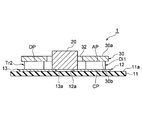
- the semiconductor module 1 includes a circuit board 10, a first transistor Tr 1, a second transistor Tr 2, at least one surge voltage absorbing element 20, and a conductive plate (plate member) 30.
- FIG. 2 is a schematic diagram showing the main configuration on the circuit board when the cross section along the line II-II in FIG. 1 is viewed in the direction of the arrow. In FIG. 2, the second conductor W2 and the case C shown in FIG. 1 are omitted.
- the semiconductor module 1 may include a first diode Di1 and a second diode Di2. Furthermore, the semiconductor module 1 may include a case C that accommodates the circuit board 10 and the first transistor Tr1, the second transistor Tr2, and the like mounted on the circuit board 10.
- Case C is schematically shown by a one-dot chain line.
- Case C may be made of resin, for example.
- the case C may include a heat sink on which the circuit board 10 is mounted as a bottom plate, and the bottom plate and a resinous cover that covers the circuit board 10 and the like.
- the structure (the first transistor Tr1, the second transistor Tr2, etc.) on the circuit board 10 accommodated in the case C is embedded with, for example, silicone gel.
- the semiconductor module 1 includes the first diode Di1, the second diode Di2, and the case C and the three surge voltage absorbing elements 20 will be described.
- FIG. 3 is a schematic diagram showing the configuration on the circuit board when the conductive plate is removed from the semiconductor module shown in FIG.
- the circuit board 10 includes an insulating substrate 11, and a P pad 12, an N pad 13, an O pad 14, and a first control signal for the surface 11 a of the insulating substrate 11.
- a pad 15 and a second control signal pad 16 are formed.
- An auxiliary pad 17 may be formed on the surface 11a. Unless otherwise noted, the form in which the auxiliary pad 17 is formed will be described.
- the insulating substrate 11 is, for example, a ceramic substrate.
- Examples of the material of the insulating substrate 11 include AlN, SiN, and Al2O3.
- the shape of the insulating substrate 11 viewed in the thickness direction is not limited, and examples thereof include a rectangle and a square.
- a heat dissipation layer made of copper or the like may be formed on the back surface of the insulating substrate 11 (on the side opposite to the surface on which the first transistor Tr1, the second transistor Tr2, etc. are mounted).
- the P pad (first input wiring pattern) 12 is a conductive layer having a first transistor mounting region 121 and an external connection region 122, and is made of, for example, copper.
- the first transistor mounting area 121 is an area where the first transistor Tr1 is mounted. In the first transistor mounting area 121, the first diode Di1 is also mounted.
- the external connection region 122 continues from the first transistor mounting region 121 seamlessly, and is a region to which one end of the positive voltage terminal 41 is connected. The other end of the positive voltage terminal 41 is drawn out of the case C.
- the N pad (second input wiring pattern) 13 is a conductive layer having a second transistor mounting region 131, a first external connection region 132, and a second external connection region 133, and is made of, for example, copper.
- the second transistor mounting area 131 is an area where the second transistor Tr2 is mounted.
- the second diode Di2 is also mounted in the second transistor mounting region 131.
- the first external connection region 132 continues seamlessly from the second transistor mounting region 131 and is a region to which one end of the negative voltage terminal 42 is connected.
- the second external connection region 133 continues seamlessly from the second transistor mounting region 131 and is a region to which one end of the second auxiliary terminal 43 is connected.
- the second external connection region 133 is disposed on the side opposite to the first external connection region 132 with respect to the second transistor mounting region 131. The other ends of the negative voltage terminal 42 and the second auxiliary terminal 43 are drawn out of the case C.
- the N pad 13 is disposed opposite to the P pad 12. Specifically, the N pad 13 is arranged in such a manner that the edge (opposing edge) 13a of the N pad 13 is opposed to and parallel to the edge (opposing edge) 12a of the P pad 12.
- the O pad (output wiring pattern) 14 is a conductive layer to which one end of the output terminal 44 is connected, and is made of, for example, copper.
- the O pad 14 is formed away from the P pad 12 on the side opposite to the external connection region 122 with respect to the first transistor mounting region 121, and is disposed on the side of the second external connection region 133. Yes. The other end of the output terminal 44 is drawn out of the case C.
- the first control signal pad (first control wiring pattern) 15 is a conductive layer to which one end of the first control terminal 45 is connected, and is made of, for example, copper.
- the first control signal pad 15 is disposed on the side of the external connection region 122. The other end of the first control terminal 45 is drawn out of the case C.
- the second control signal pad (second control wiring pattern) 16 is a conductive layer to which one end of the second control terminal 46 is connected, and is made of, for example, copper.
- the second control signal pad 16 is disposed on the side opposite to the O pad 14 with respect to the second external connection region 133 and on the side of the second external connection region 133. The other end of the second control terminal 46 is drawn out of the case C.
- the auxiliary pad 17 is a conductive layer to which one end of the first auxiliary terminal 47 is connected, and is made of, for example, copper. In the present embodiment, the auxiliary pad 17 is disposed between the first control signal pad 15 and the external connection region 122. The other end of the first auxiliary terminal 47 is drawn out of the case C.
- the shape and arrangement of the above-described pads (P pad 12, N pad 13, O pad 14 and the like) formed on the surface 11a of the insulating substrate 11 are not limited to the forms illustrated in FIGS.
- the first transistor Tr1, the second transistor Tr2, the first diode Di1, the second diode Di2, etc. may be set as appropriate in consideration of the ease of mounting and the ease of wiring.
- the first transistor Tr1 and the second transistor Tr2 are vertical transistors and have a chip shape. Examples of the material of the first transistor Tr1 and the second transistor Tr2 include Si and wide band gap semiconductors such as GaN and Si.
- the first transistor Tr1 and the second transistor Tr2 may be a MOSFET (Metal-Oxide-Semiconductor, Field-Effect Transistor) or an insulated gate bipolar transistor (IGBT: Insulated Gate Bipolar Transistor).
- MOSFET Metal-Oxide-Semiconductor, Field-Effect Transistor
- IGBT Insulated Gate Bipolar Transistor
- the first transistor Tr1 has a source electrode pad SP, a gate electrode pad GP, and a drain electrode pad DP.
- the source electrode pad SP and the gate electrode pad GP are arranged on the surface of the first transistor Tr1 opposite to the drain electrode pad DP in the thickness direction of the first transistor Tr1 (thickness direction of the insulating substrate 11).
- the drain electrode pad DP disposed to face the first transistor mounting region 121 is indicated by a broken line slightly inside the outer shape of the first transistor Tr1, but the drain electrode pad DP is
- the first transistor Tr1 may be formed on the entire surface on the opposite side of the source electrode pad SP and the gate electrode pad GP. In the first transistor Tr1, the conduction state between the source electrode pad SP and the drain electrode pad DP is controlled in accordance with a control signal applied to the gate electrode pad GP. Thereby, the first transistor Tr1 functions as a switching element.
- the drain electrode pad DP, the source electrode pad SP, and the gate electrode pad GP of the first transistor Tr1 are the first main electrode pad, the second main electrode pad, and the first gate electrode pad of the first transistor Tr1. .
- the first transistor Tr1 is mounted on the circuit board 10 so that the drain electrode pad DP faces the first transistor mounting region 121 of the P pad 12 and is electrically connected to the first transistor mounting region 121. Yes.
- the drain electrode pad DP can be fixed to the first transistor mounting region 121 through, for example, solder, a sintered material, or the like.
- the source electrode pad SP and the gate electrode pad GP of the first transistor Tr1 are disposed on the surface of the first transistor Tr1 on the opposite side to the circuit board 10.
- the gate electrode pad GP of the first transistor Tr1 is connected to the first control signal pad 15 by a first conducting wire (first connecting portion) W1. Examples of the first conductive wire W1 include a wire and a ribbon.
- drain electrode pad DP of the first transistor Tr1 Since the drain electrode pad DP of the first transistor Tr1 is electrically connected to the P pad 12, a positive voltage can be input to the drain electrode pad DP of the first transistor Tr1 via the positive voltage terminal 41. Since the gate electrode pad GP of the first transistor Tr1 is electrically connected to the first control signal pad 15 via the first conductor W1, the first transistor Tr1 is controlled via the first control terminal 45. A signal can be input.
- the second transistor Tr2 has a source electrode pad SP, a gate electrode pad GP, and a drain electrode pad DP.
- the source electrode pad SP and the gate electrode pad GP are arranged on the surface of the second transistor Tr2 opposite to the drain electrode pad DP in the thickness direction of the second transistor Tr2 (thickness direction of the insulating substrate 11). .
- the conduction state between the source electrode pad SP and the drain electrode pad DP is controlled in accordance with a control signal applied to the gate electrode pad GP. Thereby, the second transistor Tr2 functions as a switching element.
- the drain electrode pad DP, the source electrode pad SP, and the gate electrode pad GP of the second transistor Tr2 are the third main electrode pad, the fourth main electrode pad, and the second gate electrode pad of the second transistor Tr2. .
- the second transistor Tr2 is mounted on the circuit board 10 so that the source electrode pad SP and the gate electrode pad GP face the circuit board 10. Specifically, the source electrode pad SP of the second transistor Tr2 faces the second transistor mounting region 131 of the N pad 13 and is electrically connected to the second transistor mounting region 131.
- the gate electrode pad GP of Tr2 is mounted on the circuit board 10 so as to face the second control signal pad 16 and be electrically connected to the second control signal pad 16.
- the source electrode pad SP and the gate electrode pad GP of the second transistor Tr2, and the second transistor mounting region 131 and the second control signal pad 16 can be fixed through, for example, solder, a sintered material, or the like. In such a mounted state of the second transistor Tr2, the drain electrode pad DP is located on the surface of the second transistor Tr2 on the side opposite to the circuit board 10.
- a negative voltage can be input to the source electrode pad SP of the second transistor Tr2 via the negative voltage terminal 42.
- the potential of the source electrode pad SP of the second transistor Tr2 can be taken out of the semiconductor module 1 through the second auxiliary terminal 43.
- the potential of the source electrode pad SP of the second transistor Tr2 taken out via the second auxiliary terminal 43 can be used, for example, to generate a control signal for the second transistor Tr2. Since the gate electrode pad GP of the second transistor Tr2 and the second control signal pad 16 are electrically connected, a control signal can be input to the second transistor Tr2 via the second control terminal 46.
- Each of the first diode Di1 and the second diode Di2 is a free-wheeling diode for the first transistor Tr1 and the second transistor Tr2.
- the first diode Di1 and the second diode Di2 have the same configuration.
- the first diode Di1 is mounted on the circuit board 10 so that the cathode CP faces the first transistor mounting region 121 and is electrically connected to the first transistor mounting region 121.
- the cathode CP disposed opposite to the first transistor mounting region 121 is indicated by a broken line slightly inside the outer shape of the first diode Di1, but the cathode CP is the first diode Di1.
- the anode may be formed on the entire surface opposite to the anode AP.
- the cathode CP of the first diode Di1 can be fixed to the first transistor mounting region 121 via, for example, solder, a sintered material, or the like.
- the cathode CP of the first diode Di and the drain electrode pad DP of the first transistor Tr1 are electrically connected via the first transistor mounting region 121, and the positive voltage supplied from the positive voltage terminal 41 is It can also be supplied to the cathode CP of the first diode Di1.
- the anode AP of the first diode Di1 is located on the surface of the first diode Di1 on the opposite side to the circuit board 10.
- the second diode Di2 is mounted on the circuit board 10 so that the anode AP faces the second transistor mounting region 131 and is electrically connected to the second transistor mounting region 131.
- the anode AP disposed opposite to the second transistor mounting region 131 is indicated by a broken line slightly inside the outer shape of the second diode Di2, but the anode AP is the second diode Di2.
- the entire surface on the opposite side of the cathode CP can be formed.
- the anode AP of the second diode Di2 can be fixed to the second transistor mounting region 131 via, for example, solder, a sintered material, or the like.
- the anode AP of the second diode Di2 and the source electrode pad SP of the second transistor Tr2 are electrically connected via the second transistor mounting region 131 and supplied from the negative voltage terminal 42 to the second transistor Tr2.
- the negative voltage may also be supplied to the anode AP of the second diode Di2.
- the cathode CP of the second diode Di2 is located on the surface of the second diode Di2 on the side opposite to the circuit board 10.
- the surge voltage absorbing element 20 is an element for absorbing a surge voltage.
- An example of the surge voltage absorbing element 20 is a capacitor, and an example of the surge voltage absorbing capacitor is a ceramic capacitor.
- condenser for surge absorption should just be a capacity
- the surge voltage absorbing element 20 connects between the edge 12a of the P pad 12 and the edge 13a of the N pad 13. Specifically, one end of the surge voltage absorbing element 20 is connected to the first transistor mounting region 121 portion of the edge portion 12a, and the other end is connected to the second transistor mounting region 131 portion of the edge portion 13a. Has been.
- the plurality of surge voltage absorbing elements 20 are spaced apart from each other in the extending direction of the edge 12a (edge 13a).
- the conductive plate 30 includes the first transistor Tr1, the first diode Di1, the second diode Di2, and the first transistor Tr1, the first diode Di1, the second transistor Tr2, and the second diode Di2 between the circuit board 10 and the conductive plate 30. It is provided on the two transistors Tr2 and the second diode Di2.
- the conductive plate 30 may be a plate-like member made of a conductive material, for example, a metal plate. Examples of the material of the conductive plate 30 include copper or aluminum.
- the thickness of the conductive plate 30 is, for example, about 0.3 mm.
- the conductive plate 30 is made of a conductive material
- the front surface 30a of the conductive plate 30 is a conductive region (front-side conductive region)
- the back surface 30b is also a conductive region (back-side conductive region).
- the back surfaces 30b are electrically connected to each other.
- the conductive plate 30 has a substantially rectangular shape or a substantially square shape when viewed in the thickness direction (that is, in plan view), and is cut at a portion facing the gate electrode pad GP of the first transistor Tr1. It has a notch 31.
- the conductive plate 30 is disposed on the first transistor Tr1, the first diode Di1, the second transistor Tr2, and the second diode Di2 so that the gate electrode pad GP of the first transistor Tr1 is exposed from the notch 31. .
- the conductive plate 30 is fixed to the source electrode pad SP of the first transistor Tr1, the anode AP of the first diode Di1, the drain electrode pad DP of the second transistor Tr2, and the cathode CP of the second diode Di2, for example, with solder or a sintered material. Are electrically connected.
- the source electrode pad SP of the first transistor Tr1, the anode AP of the first diode Di1, the drain electrode pad DP of the second transistor Tr2, and the cathode CP of the second diode Di2 are electrically connected to each other through the conductive plate 30. It is connected to the.
- the conductive plate 30 has a through hole 32 at a portion corresponding to the position of the surge voltage absorbing element 20.
- the through hole 32 is a hole through which the surge voltage absorbing element 20 is passed, and may have a size such that the surge voltage absorbing element 20 and the through hole 32 do not contact each other. Thereby, even if the conductive plate 30 is disposed opposite to the circuit board 10, interference between the conductive plate 30 and the surge voltage absorbing element 20 is reliably prevented.
- the conductive plate 30 is connected to the O pad 14 by the second conductive wire W2.
- Examples of the second conductor W2 include a wire and a ribbon. Since a large current easily flows between the conductive plate 30 and the O pad 14, when the second conductive wire W2 is, for example, a wire, the conductive plate 30 and the O pad 14 may be connected by a plurality of wires.
- the conductive plate 30 is connected to the auxiliary pad 17 by the third conductive wire W3.
- Examples of the third conductor W3 include a wire and a ribbon.
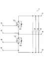
- the semiconductor module 1 functions as the power conversion circuit 2 like the equivalent circuit of the semiconductor module 1 shown in FIG.
- the power conversion circuit 2 shown in FIG. 4 is a single-phase inverter circuit.
- the semiconductor module 1 is, for example, a 2-in-1 type semiconductor module.
- circuit elements corresponding to the elements of the semiconductor module 1 are denoted by the same reference numerals.
- the first transistor Tr1 and the second transistor Tr2 included in the semiconductor module 1 constitute an upper arm and a lower arm in the power conversion circuit 2, respectively.
- the output voltage of the power conversion circuit 2 can be taken out of the semiconductor module 1 through the output terminal 44. Since the conductive plate 30 is connected to the auxiliary pad 17 by the third conductive wire W3, the potential of the source electrode pad SP of the first transistor Tr1 is taken out of the semiconductor module 1 through the first auxiliary terminal 47. obtain. The potential of the source electrode pad SP of the first transistor Tr1 taken out via the first auxiliary terminal 47 can be used, for example, to generate a control signal for the first transistor Tr1.
- the drain electrode pad DP of the first transistor Tr1 is electrically connected to the P pad 12, and the source electrode pad SP of the second transistor Tr2 is electrically connected to the N pad 13. Therefore, the positive voltage terminal 41 and the negative voltage terminal 42 can supply power to the first transistor Tr1 and the second transistor Tr2 that are electrically connected in series between the positive voltage terminal 41 and the negative voltage terminal 42. is there.
- the gate electrode pad GP of the first transistor Tr1 and the gate electrode pad GP of the second transistor Tr2 are electrically connected to the first control terminal 45 and the second control terminal 46, respectively. Therefore, a control signal can be supplied to the first transistor Tr1 and the second transistor Tr2 via the first control terminal 45 and the second control terminal 46.
- the DC voltage applied between the positive voltage terminal 41 and the negative voltage terminal 42 is changed to the AC voltage by alternately turning on / off the first transistor Tr1 and the second transistor Tr2. And an AC voltage can be output from the output terminal 44.
- each of the first transistor Tr1 and the second transistor Tr2 is turned on or off. When this occurs, a surge voltage is generated.
- the first transistor mounting region 121 of the P pad 12 and the second transistor mounting region 131 of the N pad 13 are connected to each other by the surge voltage absorbing element 20. Therefore, as shown in FIG. 4, the surge voltage absorbing element 20 is connected to the first transistor Tr1 and the second transistor Tr2 that are electrically connected in series between the positive voltage terminal 41 and the negative voltage terminal 42. In contrast, they are electrically connected in parallel. Therefore, in the configuration of the semiconductor module 1, the surge voltage absorbing element 20 can absorb the surge voltage.
- the magnitude of the surge voltage is determined by L ⁇ di / dt, where i is the current and L is the inductance.
- the inductance that defines the magnitude of the surge voltage includes the wiring inductance of the path through which the current i flows.
- di / dt depends on the switching speed of the first transistor Tr1 and the second transistor Tr2. Since switching speed has been increased, di / dt tends to increase. In particular, when a wide bandgap semiconductor is used as the material of the first transistor Tr1 and the second transistor Tr2, the switching speed is faster than that of Si, so di / dt tends to increase.
- the surge voltage absorption element 20 is disposed close to the physical (length of the electrical wiring) with respect to the first transistor Tr1 and the second transistor Tr2, and the inductance. It is important to suppress the contribution of the wiring inductance inside the case C included in L.
- the second transistor Tr2 may be mounted on the circuit board 10 so that the drain electrode pad DP faces the circuit board 10 as in Patent Document 1, for example. Conceivable.
- the second transistor Tr2 when the P pad 12 and the N pad 13 are connected to each other by the surge voltage absorbing element 20 in order to absorb the surge voltage, the second transistor Tr2 is mounted on the O pad 14, for example.
- the second transistor Tr2 and the N pad 13 must be connected via a conductive wire. In this case, the current path (electrical wiring) between the surge voltage absorbing element 20 and the second transistor Tr2 becomes long.
- the lower arm side second transistor Tr ⁇ b> 2 is vertically inverted with respect to the upper arm side first transistor Tr ⁇ b> 1 and mounted on the circuit board 10. Therefore, while mounting the first transistor Tr1 on the P pad 12 and mounting the second transistor Tr2 on the N pad 13, the drain electrode pad DP of the second transistor Tr2 and the first transistor via the conductive plate 30.
- the first transistor Tr1 and the second transistor Tr2 are connected in series by electrically connecting the source electrode pads SP of Tr1 to each other.
- the first transistor Tr1 and the second transistor Tr2 can be mounted on the P pad 12 and the N pad 13 to which the surge voltage absorbing element 20 connects, respectively. Therefore, since the first transistor Tr1 and the second transistor Tr2 can be arranged close to the surge voltage absorbing element 20, the current path between the surge voltage absorbing element 20 and the first transistor Tr1 and the second transistor Tr2 Wiring inductance can be reduced. As a result, the surge voltage is effectively suppressed, and therefore, applied to the drain electrode pad DP of the first transistor Tr1 and the source electrode pad SP of the second transistor Tr2 in the series circuit of the first transistor Tr1 and the second transistor Tr2. Voltage can be stabilized.
- the first transistor Tr1 and the second transistor Tr2 are connected in series to the circuit board 10 via a conductive plate 30 that is disposed so as to sandwich the first transistor Tr1 and the second transistor Tr2. Therefore, the degree of freedom in design such as the shape and arrangement of pads (for example, P pad 12, N pad 13 and O pad 14) on insulating substrate 11 is improved.
- the first transistor mounting region 121 of the P pad 12 and the second transistor mounting region 131 of the N pad 13 are opposed to each other with the P pad 12 and the N pad 13 facing each other.
- the edge 12a and the edge 13a to be formed can be parallel to each other.
- the surge voltage absorbing element 20 can be arranged so that the edge 12a and the edge 13b are connected to each other.
- a current path is formed by the surge voltage absorbing element 20 between the first transistor Tr1 and the second transistor Tr2 in a direction orthogonal to the extending direction of the edge 12a (or the edge 13b).
- the current path between the voltage absorbing element 20 and the first transistor Tr1 and the second transistor Tr2 becomes shorter, and the influence of inductance can be further reduced. Further, since the P pad 12 and the N pad 13 can be arranged close to each other, the semiconductor module 1 can be reduced in size.
- the degree of freedom of design of the P pad 12, the N pad 13 and the O pad 14 on the insulating substrate 11 is improved, for example, the degree of freedom of arrangement of the O pad 14 is also improved. Therefore, the design of the semiconductor module 1 is easy.
- the second transistor Tr ⁇ b> 2 and the second diode Di ⁇ b> 2 are vertically inverted with respect to the first transistor Tr ⁇ b> 1 and the first diode Di ⁇ b> 1 and mounted on the circuit board 10. For this reason, the source electrode pad SP of the first transistor Tr1, the anode AP of the first diode Di1, the drain electrode pad DP of the second transistor Tr2 and the second conductive plate 30 disposed opposite to the circuit board 10 are used. Electrical connection between the cathodes CP of the diodes Di2 is possible. Therefore, the semiconductor module 1 in which the surge voltage is suppressed by connecting the P pad 12 and the N pad 13 with the surge voltage absorbing element 20 can be manufactured at low cost.
- the conductive plate 30 has a notch 31 at a portion facing the gate electrode pad GP of the first transistor Tr1. Therefore, even if the conductive plate 30 is arranged so that the first transistor Tr1 and the second transistor Tr2 are sandwiched between the circuit board 10 and the conductive plate 30, the gate electrode pad GP of the first transistor Tr1 is surely separated from the conductive plate 30. Therefore, the gate electrode pad GP and the first control signal pad 15 can be easily connected by the first conductive wire W1.
- the thickness (or height) of the surge voltage absorbing element 20 tends to be thicker than the thickness of the first transistor Tr1 and the second transistor Tr2.
- the conductive plate 30 provided in the semiconductor module 1 has a through hole 32 for passing the surge voltage absorbing element 20. Therefore, even if the P pad 12 and the N pad 13 are connected to each other by the surge voltage absorbing element 20, by passing the surge voltage absorbing element 20 through the through hole 32 of the conductive plate 30, the conductive plate 30 can absorb the surge voltage. Physical interference with the element 20 can be prevented. Therefore, the conductive plate 30 can be disposed so that the first transistor Tr1 and the second transistor Tr2 are sandwiched between the circuit board 10 and the conductive plate 30.
- the conductive plate 30 is, for example, in the thickness direction (that is, in plan view), for example, the first transistor mounting region 121 and the second transistor mounting region. It can be manufactured as a plate-like member that covers 131. Therefore, the manufacture of the conductive plate 30 is easy, and the manufacturing cost of the semiconductor module 1 can be reduced also from this viewpoint.
- the surge voltage can be more reliably suppressed.
- a capacitor is illustrated as a surge voltage absorbing element.
- the surge voltage absorbing element may be any element that can absorb the surge voltage.
- an RC circuit or RC snubber element in which a capacitor and a resistor are combined may be used.
- FIG. 1 illustrates an example in which one first transistor is mounted on the P pad and one second transistor is mounted on the N pad.
- the number of first transistors may be plural, and the number of second transistors may be plural.
- FIG. 5 shows an example of a semiconductor module including three first transistors Tr1 and three second transistors Tr2.
- FIG. 6 shows a power conversion circuit 2A that is an equivalent circuit of the semiconductor module 1A shown in FIG.
- three first diodes Di1 are provided corresponding to the three first transistors Tr1
- three second diodes Di2 are illustrated corresponding to the three second transistors Tr2.
- the number of diodes may be different from the number of transistors.
- the mounting state of the first transistor Tr1, the first diode Di1, the second transistor Tr2, and the second diode Di2 in the semiconductor module 1A on the circuit board 10 is the same as that of the semiconductor module 1.
- the conductive plate 30 cuts corresponding to the gate electrode pad GP of each first transistor Tr1 so that the gate electrode pad GP of each first transistor Tr1 is exposed. What is necessary is just to have the notch part 31.
- FIG. The second control signal pad 16 and the N pad 13 are formed such that the three second transistors Tr2 can realize the connection relationship with the second control signal pad 16 and the N pad 13 described in the above embodiment, respectively. That's fine.
- a plurality of first transistors Tr1 are connected in parallel and a plurality of second transistors Tr2 are connected in parallel as in a power conversion circuit 2A that is an equivalent circuit of the semiconductor module 1A. Therefore, a large current can flow through the semiconductor module 1A.
- the semiconductor module is not limited to a single-phase power conversion circuit configuration such as a single-phase inverter circuit, and may have a two-phase or three-phase power conversion circuit configuration.
- the semiconductor module only needs to include at least one first transistor and one second transistor. Similarly, the semiconductor module only needs to include at least one surge voltage absorbing element.
- the arrangement state of the first transistor and the second transistor and the wiring structure between the first transistor and the second transistor and various pads are not limited to those illustrated, but the surge voltage It is preferable that the wiring inductance is optimized to minimize the wiring inductance.
- the circuit board may not have an output wiring pattern.
- one end of the output terminal may be directly connected to the conductive plate, or an output terminal provided integrally with the conductive plate may be used.
- the example of the plate member included in the semiconductor module is not limited to the conductive plate.
- the plate-like member may have a configuration in which a conductive layer (back side conductive region) is formed on the back side (surface on the circuit board side) of the insulating substrate.
- the plate-like member may be a member having a surface side conductive region electrically connected to the back side conductive region.
- a conductive layer (back side conductive region) is formed on the back surface (surface on the circuit board side) of the insulating substrate, and a conductive layer (surface side conductive region) is formed on the surface of the insulating substrate.
- the conductive layers on the front surface and the back surface of the insulating substrate may be electrically connected to each other.
- the plate-shaped member has the back-side conductive region and the front-side conductive region and the circuit board has the output wiring pattern as described above, for example, the front-side conductive region and the output wiring pattern are electrically connected to each other.
- the back side conductive region and the output wiring pattern can be electrically connected to each other.
- the plate-like member has the back-side conductive region and the front-side conductive region and the circuit board does not have the output wiring pattern, for example, one end of the output terminal is directly connected to the front-side conductive region.
- the back side conductive region and the output terminal may be electrically connected to each other.
- SYMBOLS 1,1A Semiconductor module, 10 ... Circuit board, 11 ... Insulating board, 12 ... P pad (1st input wiring pattern), 12a ... Edge part (opposing edge part), 13 ... N pad (2nd input wiring) Pattern), 13a... Edge (opposite edge), 14... O pad (output wiring pattern), 15... First control signal pad (first control wiring pattern), 16. Second control wiring pattern), 20 ... surge voltage absorbing element, DP ... drain electrode pad (first main electrode pad, third main electrode pad), GP ... gate electrode pad (first gate electrode pad, second gate electrode) Pad), SP ... source electrode pad (second main electrode pad, fourth main electrode pad), Tr1 ... first transistor (first vertical transistor), Tr2 ... second transistor (second vertical transistor).
Abstract
A semiconductor module according to one form of this invention comprises: a circuit board, a first vertical transistor in which a first main electrode pad faces and is connected to the first input wiring pattern of a circuit board, and a first gate electrode pad is connected to the first control wiring pattern of the circuit board; a second vertical transistor in which a fourth electrode pad faces and is connected to the second input wiring pattern of the circuit board, and a second gate electrode pad faces and is connected to the second control wiring pattern of the circuit board; a surge voltage absorption element which is connected to the first and second input wiring patterns and absorbs a surge voltage; and a plate-shaped member connecting a second main electrode pad of the first vertical transistor and a third main electrode pad of the second vertical transistor.
Description
本開示は半導体モジュールに関する。
This disclosure relates to semiconductor modules.
本出願は、2016年11月24日出願の日本出願第2016-227744号に基づく優先権を主張し、前記日本出願に記載された全ての記載内容を援用するものである。
This application claims priority based on Japanese Patent Application No. 2016-227744 filed on November 24, 2016, and incorporates all the contents described in the Japanese application.
インバータ回路といった電力変換回路を含む半導体モジュールでは、上アーム及び下アームを構成するスイッチング素子であるトランジスタをターンオン又はターンオフした直後に、電力変換回路の正側入力端子と負側入力端子の間にサージ電圧が発生することが知られている。上記サージ電圧を抑制するために、特許文献1では、サージ電圧吸収素子としてのスナバコンデンサを、正側入力端子と負側入力端子との間に接続している。
In a semiconductor module including a power conversion circuit such as an inverter circuit, a surge is generated between the positive input terminal and the negative input terminal of the power conversion circuit immediately after turning on or off a transistor that is a switching element constituting the upper arm and the lower arm. It is known that a voltage is generated. In order to suppress the surge voltage, in Patent Document 1, a snubber capacitor as a surge voltage absorbing element is connected between the positive input terminal and the negative input terminal.
本開示の一側面に係る半導体モジュールは、(A)絶縁基板と、上記絶縁基板の表面上に形成された第1入力用配線パターン、第2入力用配線パターン、第1制御用配線パターン及び第2制御用配線パターンとを有する回路基板と、(B)第1主電極パッド、第2主電極パッド及び第1ゲート電極パッドを有する第1縦型トランジスタであって、上記第2主電極パッド及び上記第1ゲート電極パッドは上記第1主電極パッドと反対側に形成されており、上記第1主電極パッドが上記第1入力用配線パターンと対向し且つ上記第1入力用配線パターンに電気的に接続された状態で上記回路基板に搭載され、上記第1ゲート電極パッドは上記第1制御用配線パターンに電気的に接続される上記第1縦型トランジスタと、(C)第3主電極パッド、第4主電極パッド及び第2ゲート電極パッドを有する第2縦型トランジスタであって、上記第4主電極パッド及び上記第2ゲート電極パッドは上記第3主電極パッドと反対側に形成されており、上記第4主電極パッドが上記第2入力用配線パターンと対向し且つ上記第2入力用配線パターンに電気的に接続されるとともに、上記第2ゲート電極パッドが上記第2制御用配線パターンと対向し且つ上記第2制御用配線パターンに電気的に接続された状態で上記回路基板に搭載される上記第2縦型トランジスタと、(D)上記第1入力用配線パターンと上記第2入力用配線パターンとの間を接続しておりサージ電圧を吸収するサージ電圧吸収素子と、(E)上記第1縦型トランジスタ及び上記第2縦型トランジスタ上に配置されており、裏面側導電領域を有する板状部材と、を備え、上記第2主電極パッドと上記第3主電極パッドとは、上記板状部材の上記裏面側導電領域によって互いに電気的に接続される。
A semiconductor module according to one aspect of the present disclosure includes: (A) an insulating substrate; a first input wiring pattern formed on a surface of the insulating substrate; a second input wiring pattern; a first control wiring pattern; 2 a first vertical transistor having a circuit board having a control wiring pattern, and (B) a first main electrode pad, a second main electrode pad, and a first gate electrode pad, wherein the second main electrode pad and The first gate electrode pad is formed on the side opposite to the first main electrode pad, the first main electrode pad is opposed to the first input wiring pattern and electrically connected to the first input wiring pattern. And the first gate electrode pad mounted on the circuit board in a state of being connected to the first vertical transistor electrically connected to the first control wiring pattern, and (C) a third main electrode pad. A second vertical transistor having a fourth main electrode pad and a second gate electrode pad, wherein the fourth main electrode pad and the second gate electrode pad are formed on a side opposite to the third main electrode pad. The fourth main electrode pad faces the second input wiring pattern and is electrically connected to the second input wiring pattern, and the second gate electrode pad is connected to the second control wiring pattern. The second vertical transistor mounted on the circuit board in a state of being opposed to and electrically connected to the second control wiring pattern; and (D) the first input wiring pattern and the second input wiring. A surge voltage absorbing element connected between the wiring patterns and absorbing the surge voltage; (E) disposed on the first vertical transistor and the second vertical transistor; And a plate-like member having a conductive region, said a second main electrode pad and the third main electrode pads are electrically connected to each other by the back surface side conductive region of the plate-like member.
特許文献1に記載の技術では、スナバコンデンサ(サージ電圧吸収素子)の熱による劣化を防止するために、スイッチング素子であるトランジスタなどを実装する基板上において、トランジスタを実装する部分と、スナバコンデンサを実装する部分とを別々に形成し、それらを熱的に分離している。この場合、トランジスタと、スナバコンデンサとの距離が長くなる傾向にあるため、サージ電圧を十分に抑制できないおそれがある。
In the technique described in Patent Document 1, in order to prevent deterioration of the snubber capacitor (surge voltage absorption element) due to heat, a portion on which a transistor is mounted and a snubber capacitor are mounted on a substrate on which a transistor as a switching element is mounted. The parts to be mounted are formed separately and are thermally separated. In this case, since the distance between the transistor and the snubber capacitor tends to be long, the surge voltage may not be sufficiently suppressed.
そこで、サージ電圧をより確実に抑制可能な半導体モジュールを提供することを本開示の目的の1つとする。
Therefore, it is an object of the present disclosure to provide a semiconductor module that can more reliably suppress a surge voltage.
以下、図面を参照して本開示の技術の実施形態について説明する。図面の説明において、同一要素には同一符号を付し、重複する説明を省略する。
[実施形態の説明]
最初に、本開示の技術の実施形態の内容を列記して説明する。 Hereinafter, embodiments of the technology of the present disclosure will be described with reference to the drawings. In the description of the drawings, the same elements are denoted by the same reference numerals, and redundant description is omitted.
[Description of Embodiment]
First, the contents of the embodiments of the technology of the present disclosure will be listed and described.
本開示の一側面に係る半導体モジュールは、(A)絶縁基板と、上記絶縁基板の表面上に形成された第1入力用配線パターン、第2入力用配線パターン、第1制御用配線パターン及び第2制御用配線パターンとを有する回路基板と、(B)第1主電極パッド、第2主電極パッド及び第1ゲート電極パッドを有する第1縦型トランジスタであって、上記第2主電極パッド及び上記第1ゲート電極パッドは上記第1主電極パッドと反対側に形成されており、上記第1主電極パッドが上記第1入力用配線パターンと対向し且つ上記第1入力用配線パターンに電気的に接続された状態で上記回路基板に搭載され、上記第1ゲート電極パッドは上記第1制御用配線パターンに電気的に接続される上記第1縦型トランジスタと、(C)第3主電極パッド、第4主電極パッド及び第2ゲート電極パッドを有する第2縦型トランジスタであって、上記第4主電極パッド及び上記第2ゲート電極パッドは上記第3主電極パッドと反対側に形成されており、上記第4主電極パッドが上記第2入力用配線パターンと対向し且つ上記第2入力用配線パターンに電気的に接続されるとともに、上記第2ゲート電極パッドが上記第2制御用配線パターンと対向し且つ上記第2制御用配線パターンに電気的に接続された状態で上記回路基板に搭載される上記第2縦型トランジスタと、(D)上記第1入力用配線パターンと上記第2入力用配線パターンとの間を接続しておりサージ電圧を吸収するサージ電圧吸収素子と、(E)上記第1縦型トランジスタ及び上記第2縦型トランジスタ上に配置されており、裏面側導電領域を有する板状部材と、を備え、上記第2主電極パッドと上記第3主電極パッドとは、上記板状部材の上記裏面側導電領域によって互いに電気的に接続される。
A semiconductor module according to one aspect of the present disclosure includes: (A) an insulating substrate; a first input wiring pattern formed on a surface of the insulating substrate; a second input wiring pattern; a first control wiring pattern; 2 a first vertical transistor having a circuit board having a control wiring pattern, and (B) a first main electrode pad, a second main electrode pad, and a first gate electrode pad, wherein the second main electrode pad and The first gate electrode pad is formed on the side opposite to the first main electrode pad, the first main electrode pad is opposed to the first input wiring pattern and electrically connected to the first input wiring pattern. And the first gate electrode pad mounted on the circuit board in a state of being connected to the first vertical transistor electrically connected to the first control wiring pattern, and (C) a third main electrode pad. A second vertical transistor having a fourth main electrode pad and a second gate electrode pad, wherein the fourth main electrode pad and the second gate electrode pad are formed on a side opposite to the third main electrode pad. The fourth main electrode pad faces the second input wiring pattern and is electrically connected to the second input wiring pattern, and the second gate electrode pad is connected to the second control wiring pattern. The second vertical transistor mounted on the circuit board in a state of being opposed to and electrically connected to the second control wiring pattern; and (D) the first input wiring pattern and the second input wiring. A surge voltage absorbing element connected between the wiring patterns and absorbing the surge voltage; (E) disposed on the first vertical transistor and the second vertical transistor; And a plate-like member having a conductive region, said a second main electrode pad and the third main electrode pads are electrically connected to each other by the back surface side conductive region of the plate-like member.
上記構成では、第1縦型トランジスタの第2主電極パッドと第2縦型トランジスタの第3主電極パッドとが板状部材の裏面側導電領域を介して電気的に接続されていることから、第1縦型トランジスタ及び第2縦型トランジスタは直列接続されている。第1縦型トランジスタの第1主電極パッドが第1入力用配線パターンに電気的に接続されており、第2縦型トランジスタの第4主電極パッドが第2入力用配線パターに接続されている。よって、第1縦型トランジスタ及び第2縦型トランジスタの直列回路に対して、第1入力用配線パターンを介して、第1縦型トランジスタに正電圧を供給し、第2入力用配線パターンを介して第2縦型トランジスタに負電圧を供給できる。このように、第1縦型トランジスタに正電圧を供給し、第2縦型トランジスタに負電圧を供給した状態で、第1制御用配線パターン及び第2制御用配線パターンを介して第1縦型トランジスタの第1ゲート電極パッド及び第2縦型トランジスタの第2ゲート電極パッドに制御信号を入力することで、半導体モジュールは電力変換回路として機能する。半導体モジュールでは、第1入力用配線パターン及び第2入力用配線パターンがサージ電圧吸収素子で接続されていることから、半導体モジュールの動作時に生じるサージ電圧を吸収できる。第1縦型トランジスタは、第1主電極が第1入力用配線パターンと対向し且つ第1入力用配線パターンに電気的に接続された状態で回路基板に搭載されており、第2縦型トランジスタは、第4主電極パッドが第2入力用配線パターンと対向し且つ第2入力用配線パターンに電気的に接続された状態で回路基板に搭載されている。そのため、第1縦型トランジスタ及び第2縦型トランジスタからサージ電圧吸収素子までの電流経路を短縮できるので、インダクタンスを低減できる。その結果、半導体モジュールの動作時に生じるサージ電圧をより確実に抑制可能である。
In the above configuration, the second main electrode pad of the first vertical transistor and the third main electrode pad of the second vertical transistor are electrically connected via the back surface side conductive region of the plate member. The first vertical transistor and the second vertical transistor are connected in series. The first main electrode pad of the first vertical transistor is electrically connected to the first input wiring pattern, and the fourth main electrode pad of the second vertical transistor is connected to the second input wiring pattern. . Therefore, a positive voltage is supplied to the first vertical transistor via the first input wiring pattern for the series circuit of the first vertical transistor and the second vertical transistor via the second input wiring pattern. Thus, a negative voltage can be supplied to the second vertical transistor. In this manner, the first vertical type is supplied via the first control wiring pattern and the second control wiring pattern in a state where a positive voltage is supplied to the first vertical transistor and a negative voltage is supplied to the second vertical transistor. By inputting control signals to the first gate electrode pad of the transistor and the second gate electrode pad of the second vertical transistor, the semiconductor module functions as a power conversion circuit. In the semiconductor module, since the first input wiring pattern and the second input wiring pattern are connected by the surge voltage absorbing element, the surge voltage generated during the operation of the semiconductor module can be absorbed. The first vertical transistor is mounted on the circuit board with the first main electrode facing the first input wiring pattern and electrically connected to the first input wiring pattern. The second vertical transistor Is mounted on the circuit board with the fourth main electrode pad facing the second input wiring pattern and electrically connected to the second input wiring pattern. As a result, the current path from the first vertical transistor and the second vertical transistor to the surge voltage absorbing element can be shortened, so that the inductance can be reduced. As a result, the surge voltage generated during the operation of the semiconductor module can be more reliably suppressed.
上記板状部材は、切欠き部を有し、上記板状部材は、上記切欠き部から上記第1ゲート電極パッドを露出するように、上記第1縦型トランジスタ上に配置されていてもよい。これにより、板状部材を、第1縦型トランジスタ及び第2縦型トランジスタからみて回路基板と反対側に配置しても、第1縦型トランジスタの第1ゲート電極パッドと、第1制御用配線パターンとを容易に接続できる。
The plate-like member may have a notch, and the plate-like member may be disposed on the first vertical transistor so that the first gate electrode pad is exposed from the notch. . Thus, even if the plate-like member is disposed on the side opposite to the circuit board as viewed from the first vertical transistor and the second vertical transistor, the first gate electrode pad of the first vertical transistor and the first control wiring The pattern can be easily connected.
上記板状部材は、上記板状部材を貫通する貫通孔を有し、上記サージ電圧吸収素子は、上記貫通孔内に配置されていてもよい。これにより、サージ電圧吸収素子と板状部材との干渉を防止できる。
The plate-like member may have a through-hole penetrating the plate-like member, and the surge voltage absorbing element may be disposed in the through-hole. Thereby, interference with a surge voltage absorption element and a plate-shaped member can be prevented.
上記第1入力用配線パターンにおける上記第1縦型トランジスタが搭載される第1トランジスタ搭載領域と、上記第2入力用配線パターンにおける上記第2縦型トランジスタが搭載される第2トランジスタ搭載領域とは対向配置されており、上記第1トランジスタ搭載領域と上記第2トランジスタ搭載領域の互いに対向する対向縁部は平行であり、上記サージ電圧吸収素子は、上記第1トランジスタ搭載領域と上記第2トランジスタ搭載領域それぞれの上記対向縁部の間を接続していてもよい。
A first transistor mounting area in which the first vertical transistor is mounted in the first input wiring pattern and a second transistor mounting area in which the second vertical transistor is mounted in the second input wiring pattern. The opposing edge portions of the first transistor mounting region and the second transistor mounting region that face each other are parallel to each other, and the surge voltage absorbing element includes the first transistor mounting region and the second transistor mounting. You may connect between the said opposing edge parts of each area | region.
これにより、対向縁部の延在方向と直交する方向において、第1縦型トランジスタと第2縦型トランジスタとの間にサージ電圧吸収素子を配置可能である。そのため、第1縦型トランジスタ及び第2縦型トランジスタからサージ電圧吸収素子までの電流経路をより短くできる。その結果、半導体モジュールの動作時に生じるサージ電圧を、一層効率的に抑制可能である。
Thereby, a surge voltage absorbing element can be disposed between the first vertical transistor and the second vertical transistor in a direction orthogonal to the extending direction of the opposing edge. Therefore, the current path from the first vertical transistor and the second vertical transistor to the surge voltage absorption element can be further shortened. As a result, the surge voltage generated during the operation of the semiconductor module can be more efficiently suppressed.
上記回路基板は、上記絶縁基板上に出力用配線パターンを有し、上記出力用配線パターンは、上記板状部材の上記裏面側導電領域と電気的に接続されていてもよい。この場合、出力用配線パターンを介して、出力電力を取り出し得る。
The circuit board may have an output wiring pattern on the insulating substrate, and the output wiring pattern may be electrically connected to the back-side conductive region of the plate-like member. In this case, the output power can be taken out via the output wiring pattern.
本開示の更なる一側面に係る半導体モジュールは、上面に第1入力用配線パターン及び第2入力用配線パターンを有する回路基板と、前記回路基板の上側に配置され前記回路基板に対向する下面に裏面側導電領域を有する板状部材と、下面に第1主電極パッド、上面に第2主電極パッド及び第1ゲート電極パッドを有し、前記第1主電極パッドが前記第1入力用配線パターンと電気的に接続され且つ前記第2主電極パッドが前記裏面側導電領域と電気的に接続されるように前記回路基板と前記板状部材との間に挟まれて配置される第1縦型トランジスタと、上面に第3主電極パッド、下面に第4主電極パッド及び第2ゲート電極パッドを有し、前記第4主電極パッドが前記第2入力用配線パターンと電気的に接続され且つ前記第3主電極パッドが前記裏面側導電領域と電気的に接続されるように前記回路基板と前記板状部材との間に挟まれて配置される第2縦型トランジスタと、前記第1入力用配線パターンと前記第2入力用配線パターンとの間を接続する容量性素子と、前記第1ゲート電極パッドに電気的に接続される第1制御端子と、前記第2ゲート電極パッドに電気的に接続される第2制御端子と、前記裏面側導電領域に電気的に接続される出力端子とを含む。
A semiconductor module according to a further aspect of the present disclosure includes a circuit board having a first input wiring pattern and a second input wiring pattern on an upper surface, and a lower surface disposed on the circuit board and facing the circuit board. A plate-like member having a back-side conductive region; a first main electrode pad on a lower surface; a second main electrode pad and a first gate electrode pad on an upper surface; wherein the first main electrode pad is the first input wiring pattern. And a first vertical type sandwiched between the circuit board and the plate-like member so that the second main electrode pad is electrically connected to the back-side conductive region. A transistor having a third main electrode pad on the upper surface and a fourth main electrode pad and a second gate electrode pad on the lower surface, wherein the fourth main electrode pad is electrically connected to the second input wiring pattern; Third main electrode pad A second vertical transistor disposed between the circuit board and the plate-like member so that a gate is electrically connected to the back-side conductive region, the first input wiring pattern, and the A capacitive element that connects between the second input wiring pattern, a first control terminal that is electrically connected to the first gate electrode pad, and a second electrode that is electrically connected to the second gate electrode pad. 2 control terminals and an output terminal electrically connected to the back side conductive region.
上記半導体モジュールでは、第1入力用配線パターン及び第2入力用配線パターンが容量性素子で接続されていることから、半導体モジュールの動作時に生じるサージ電圧を吸収できる。第1縦型トランジスタは、第1主電極が第1入力用配線パターンと電気的に接続されるよう回路基板と板状部材との間に挟まれて配置され、第2縦型トランジスタは、第4主電極パッドが第2入力用配線パターンと電気的に接続されるように回路基板と板状部材との間に挟まれて配置される。そのため、第1縦型トランジスタ及び第2縦型トランジスタから容量性素子までの電流経路を短縮できるので、インダクタンスを低減できる。その結果、半導体モジュールの動作時に生じるサージ電圧をより確実に抑制可能である。
[実施形態の詳細]
本開示の技術の実施形態の具体例を、以下に図面を参照しつつ説明する。本発明はこれらの例示に限定されるものではなく、請求の範囲によって示され、請求の範囲内と均等の範囲内とでのすべての変更が含まれることが意図される。図面の説明においては同一要素には同一符号を付し、重複する説明を省略する。 In the semiconductor module, since the first input wiring pattern and the second input wiring pattern are connected by the capacitive element, the surge voltage generated during the operation of the semiconductor module can be absorbed. The first vertical transistor is disposed between the circuit board and the plate member so that the first main electrode is electrically connected to the first input wiring pattern, and the second vertical transistor The four main electrode pads are disposed between the circuit board and the plate member so as to be electrically connected to the second input wiring pattern. Therefore, since the current path from the first vertical transistor and the second vertical transistor to the capacitive element can be shortened, the inductance can be reduced. As a result, the surge voltage generated during the operation of the semiconductor module can be more reliably suppressed.
[Details of the embodiment]
Specific examples of embodiments of the technology of the present disclosure will be described below with reference to the drawings. The present invention is not limited to these exemplifications, but is defined by the scope of the claims, and is intended to include all modifications within the scope of the claims and within the equivalent scope. In the description of the drawings, the same reference numerals are given to the same elements, and duplicate descriptions are omitted.
図1及び図2に示した半導体モジュール1は、インバータ装置といった電力変換装置として機能する。半導体モジュール1は、回路基板10と、第1トランジスタTr1と、第2トランジスタTr2と、少なくとも一つのサージ電圧吸収素子20と、導電板(板状部材)30とを備える。図2は、図1のII-II線に沿った断面を矢印方向に見た場合において、回路基板上の主な構成を示す模式図である。図2では、図1に示した第2導線W2及びケースC等を省略している。
1 and 2 function as a power conversion device such as an inverter device. The semiconductor module 1 includes a circuit board 10, a first transistor Tr 1, a second transistor Tr 2, at least one surge voltage absorbing element 20, and a conductive plate (plate member) 30. FIG. 2 is a schematic diagram showing the main configuration on the circuit board when the cross section along the line II-II in FIG. 1 is viewed in the direction of the arrow. In FIG. 2, the second conductor W2 and the case C shown in FIG. 1 are omitted.
半導体モジュール1は、第1ダイオードDi1と第2ダイオードDi2とを有してもよい。更に、半導体モジュール1は、回路基板10及び回路基板10上に実装される第1トランジスタTr1、第2トランジスタTr2などを収容するケースCを備えてもよい。
The semiconductor module 1 may include a first diode Di1 and a second diode Di2. Furthermore, the semiconductor module 1 may include a case C that accommodates the circuit board 10 and the first transistor Tr1, the second transistor Tr2, and the like mounted on the circuit board 10.
図1では、ケースCを一点鎖線で模式的に示している。ケースCは、例えば樹脂で構成されてもよい。ケースCは、回路基板10が搭載される放熱板を底板とし、その底板と、回路基板10等を覆う樹脂性のカバーとから構成されてもよい。ケースC内に収容された回路基板10上の構造(第1トランジスタTr1、第2トランジスタTr2など)は、例えばシリコーンゲルで埋設されている。
In FIG. 1, the case C is schematically shown by a one-dot chain line. Case C may be made of resin, for example. The case C may include a heat sink on which the circuit board 10 is mounted as a bottom plate, and the bottom plate and a resinous cover that covers the circuit board 10 and the like. The structure (the first transistor Tr1, the second transistor Tr2, etc.) on the circuit board 10 accommodated in the case C is embedded with, for example, silicone gel.
以下では、断らない限り、半導体モジュール1が、第1ダイオードDi1、第2ダイオードDi2及びケースCを備えるとともに、3つのサージ電圧吸収素子20を備えた形態について説明する。
Hereinafter, unless otherwise specified, a configuration in which the semiconductor module 1 includes the first diode Di1, the second diode Di2, and the case C and the three surge voltage absorbing elements 20 will be described.
図3は、図1に示した半導体モジュールにおいて、導電板を取り除いた場合の回路基板上の構成を示す模式図である。図1及び図3に示したように、回路基板10は、絶縁基板11を有し、絶縁基板11の表面11a上には、Pパッド12、Nパッド13、Oパッド14、第1制御信号用パッド15及び第2制御信号用パッド16が形成されている。表面11a上には、補助パッド17が形成されていてもよい。断らない限り、補助パッド17が形成された形態を説明する。
FIG. 3 is a schematic diagram showing the configuration on the circuit board when the conductive plate is removed from the semiconductor module shown in FIG. As shown in FIGS. 1 and 3, the circuit board 10 includes an insulating substrate 11, and a P pad 12, an N pad 13, an O pad 14, and a first control signal for the surface 11 a of the insulating substrate 11. A pad 15 and a second control signal pad 16 are formed. An auxiliary pad 17 may be formed on the surface 11a. Unless otherwise noted, the form in which the auxiliary pad 17 is formed will be described.
絶縁基板11は例えばセラミックス基板である。絶縁基板11の材料の例は、AlN、SiN及びAl2O3を含む。絶縁基板11の厚さ方向に見た形状(即ち例えば上方から見た平面形状)は限定されないが、例えば矩形及び正方形が挙げられる。絶縁基板11の裏面(第1トランジスタTr1、第2トランジスタTr2などが搭載される面と反対側)には、銅などからなる放熱層が形成されてもよい。
The insulating substrate 11 is, for example, a ceramic substrate. Examples of the material of the insulating substrate 11 include AlN, SiN, and Al2O3. The shape of the insulating substrate 11 viewed in the thickness direction (that is, for example, a planar shape viewed from above) is not limited, and examples thereof include a rectangle and a square. A heat dissipation layer made of copper or the like may be formed on the back surface of the insulating substrate 11 (on the side opposite to the surface on which the first transistor Tr1, the second transistor Tr2, etc. are mounted).
Pパッド(第1入力用配線パターン)12は、第1トランジスタ搭載領域121と、外部接続領域122とを有する導電層であり、例えば銅からなる。第1トランジスタ搭載領域121は、第1トランジスタTr1が搭載される領域である。第1トランジスタ搭載領域121には、第1ダイオードDi1も搭載される。外部接続領域122は、第1トランジスタ搭載領域121から継ぎ目無く続いており、正電圧用端子41の一端が接続される領域である。正電圧用端子41の他端は、ケースC外部に引き出されている。
The P pad (first input wiring pattern) 12 is a conductive layer having a first transistor mounting region 121 and an external connection region 122, and is made of, for example, copper. The first transistor mounting area 121 is an area where the first transistor Tr1 is mounted. In the first transistor mounting area 121, the first diode Di1 is also mounted. The external connection region 122 continues from the first transistor mounting region 121 seamlessly, and is a region to which one end of the positive voltage terminal 41 is connected. The other end of the positive voltage terminal 41 is drawn out of the case C.
Nパッド(第2入力用配線パターン)13は、第2トランジスタ搭載領域131と、第1外部接続領域132と、第2外部接続領域133とを有する導電層であり、例えば銅からなる。第2トランジスタ搭載領域131は、第2トランジスタTr2が搭載される領域である。第2トランジスタ搭載領域131には、第2ダイオードDi2も搭載される。第1外部接続領域132は、第2トランジスタ搭載領域131から継ぎ目無く続いており、負電圧用端子42の一端が接続される領域である。第2外部接続領域133は、第2トランジスタ搭載領域131から継ぎ目無く続いており、第2補助端子43の一端が接続される領域である。本実施形態において、第2外部接続領域133は、第2トランジスタ搭載領域131に対して第1外部接続領域132と反対側に配置されている。負電圧用端子42及び第2補助端子43の他端は、ケースC外部に引き出されている。
The N pad (second input wiring pattern) 13 is a conductive layer having a second transistor mounting region 131, a first external connection region 132, and a second external connection region 133, and is made of, for example, copper. The second transistor mounting area 131 is an area where the second transistor Tr2 is mounted. The second diode Di2 is also mounted in the second transistor mounting region 131. The first external connection region 132 continues seamlessly from the second transistor mounting region 131 and is a region to which one end of the negative voltage terminal 42 is connected. The second external connection region 133 continues seamlessly from the second transistor mounting region 131 and is a region to which one end of the second auxiliary terminal 43 is connected. In the present embodiment, the second external connection region 133 is disposed on the side opposite to the first external connection region 132 with respect to the second transistor mounting region 131. The other ends of the negative voltage terminal 42 and the second auxiliary terminal 43 are drawn out of the case C.
Nパッド13は、Pパッド12と対向配置されている。具体的には、Nパッド13は、Nパッド13の縁部(対向縁部)13aが、Pパッド12の縁部(対向縁部)12aと対向し且つ平行の状態で配置されている。
The N pad 13 is disposed opposite to the P pad 12. Specifically, the N pad 13 is arranged in such a manner that the edge (opposing edge) 13a of the N pad 13 is opposed to and parallel to the edge (opposing edge) 12a of the P pad 12.
Oパッド(出力用配線パターン)14は、出力端子44の一端が接続される導電層であり、例えば銅からなる。本実施形態において、Oパッド14は、第1トランジスタ搭載領域121に対して外部接続領域122と反対側でPパッド12から離れて形成され、且つ第2外部接続領域133の側方に配置されている。出力端子44の他端は、ケースC外部に引き出されている。
The O pad (output wiring pattern) 14 is a conductive layer to which one end of the output terminal 44 is connected, and is made of, for example, copper. In the present embodiment, the O pad 14 is formed away from the P pad 12 on the side opposite to the external connection region 122 with respect to the first transistor mounting region 121, and is disposed on the side of the second external connection region 133. Yes. The other end of the output terminal 44 is drawn out of the case C.
第1制御信号用パッド(第1制御用配線パターン)15は、第1制御端子45の一端が接続される導電層であり、例えば銅からなる。本実施形態において、第1制御信号用パッド15は、外部接続領域122の側方に配置されている。第1制御端子45の他端は、ケースC外部に引き出されている。
The first control signal pad (first control wiring pattern) 15 is a conductive layer to which one end of the first control terminal 45 is connected, and is made of, for example, copper. In the present embodiment, the first control signal pad 15 is disposed on the side of the external connection region 122. The other end of the first control terminal 45 is drawn out of the case C.
第2制御信号用パッド(第2制御用配線パターン)16は、第2制御端子46の一端が接続される導電層であり、例えば銅からなる。本実施形態において、第2制御信号用パッド16は、第2外部接続領域133に対してOパッド14と反対側において、第2外部接続領域133の側方に配置されている。第2制御端子46の他端は、ケースC外部に引き出されている。
The second control signal pad (second control wiring pattern) 16 is a conductive layer to which one end of the second control terminal 46 is connected, and is made of, for example, copper. In the present embodiment, the second control signal pad 16 is disposed on the side opposite to the O pad 14 with respect to the second external connection region 133 and on the side of the second external connection region 133. The other end of the second control terminal 46 is drawn out of the case C.
補助パッド17は、第1補助端子47の一端が接続される導電層であり、例えば銅からなる。本実施形態において、補助パッド17は、第1制御信号用パッド15と外部接続領域122の間に配置されている。第1補助端子47の他端は、ケースC外部に引き出されている。
The auxiliary pad 17 is a conductive layer to which one end of the first auxiliary terminal 47 is connected, and is made of, for example, copper. In the present embodiment, the auxiliary pad 17 is disposed between the first control signal pad 15 and the external connection region 122. The other end of the first auxiliary terminal 47 is drawn out of the case C.
絶縁基板11の表面11a上に形成されている上述したパッド(Pパッド12、Nパッド13、Oパッド14など)の形状及び配置は、図1及び図3に例示した形態に限定されず、第1トランジスタTr1、第2トランジスタTr2、第1ダイオードDi1、第2ダイオードDi2などの搭載容易性及び配線容易性などを考慮して適宜設定されていればよい。
The shape and arrangement of the above-described pads (P pad 12, N pad 13, O pad 14 and the like) formed on the surface 11a of the insulating substrate 11 are not limited to the forms illustrated in FIGS. The first transistor Tr1, the second transistor Tr2, the first diode Di1, the second diode Di2, etc. may be set as appropriate in consideration of the ease of mounting and the ease of wiring.
第1トランジスタTr1及び第2トランジスタTr2は、縦型トランジスタであり、チップ状を呈する。第1トランジスタTr1及び第2トランジスタTr2の材料の例は、SiC、GaN等のワイドバンドギャップ半導体及びSiを含む。第1トランジスタTr1及び第2トランジスタTr2は、MOSFET(Metal-Oxide-Semiconductor Field-Effect Transistor)でもよいし、絶縁ゲートバイポーラトランジスタ(IGBT:Insulated Gate Bipolar Transistor)でもよい。以下、断らない限り、第1トランジスタTr1及び第2トランジスタTr2はMOSFETであり、互いに同じ構成を有する。
The first transistor Tr1 and the second transistor Tr2 are vertical transistors and have a chip shape. Examples of the material of the first transistor Tr1 and the second transistor Tr2 include Si and wide band gap semiconductors such as GaN and Si. The first transistor Tr1 and the second transistor Tr2 may be a MOSFET (Metal-Oxide-Semiconductor, Field-Effect Transistor) or an insulated gate bipolar transistor (IGBT: Insulated Gate Bipolar Transistor). Hereinafter, unless otherwise specified, the first transistor Tr1 and the second transistor Tr2 are MOSFETs and have the same configuration.
第1トランジスタTr1は、ソース電極パッドSPと、ゲート電極パッドGPと、ドレイン電極パッドDPとを有する。ソース電極パッドSPとゲート電極パッドGPとは、第1トランジスタTr1の厚さ方向(絶縁基板11の厚さ方向)において、ドレイン電極パッドDPと反対側の第1トランジスタTr1の面に配置されている。図3では、図示の都合上、第1トランジスタ搭載領域121と対向配置されているドレイン電極パッドDPを、第1トランジスタTr1の外形より若干内側に破線で示しているが、ドレイン電極パッドDPは、第1トランジスタTr1においてソース電極パッドSPとゲート電極パッドGPと反対側の全面に形成され得る。第1トランジスタTr1では、ゲート電極パッドGPに印加される制御信号に応じてソース電極パッドSP及びドレイン電極パッドDP間の導通状態が制御される。これにより、第1トランジスタTr1は、スイッチング素子として機能する。
The first transistor Tr1 has a source electrode pad SP, a gate electrode pad GP, and a drain electrode pad DP. The source electrode pad SP and the gate electrode pad GP are arranged on the surface of the first transistor Tr1 opposite to the drain electrode pad DP in the thickness direction of the first transistor Tr1 (thickness direction of the insulating substrate 11). . In FIG. 3, for convenience of illustration, the drain electrode pad DP disposed to face the first transistor mounting region 121 is indicated by a broken line slightly inside the outer shape of the first transistor Tr1, but the drain electrode pad DP is The first transistor Tr1 may be formed on the entire surface on the opposite side of the source electrode pad SP and the gate electrode pad GP. In the first transistor Tr1, the conduction state between the source electrode pad SP and the drain electrode pad DP is controlled in accordance with a control signal applied to the gate electrode pad GP. Thereby, the first transistor Tr1 functions as a switching element.
本実施形態において、第1トランジスタTr1のドレイン電極パッドDP、ソース電極パッドSP及びゲート電極パッドGPは、第1トランジスタTr1の第1主電極パッド、第2主電極パッド及び第1ゲート電極パッドである。
In the present embodiment, the drain electrode pad DP, the source electrode pad SP, and the gate electrode pad GP of the first transistor Tr1 are the first main electrode pad, the second main electrode pad, and the first gate electrode pad of the first transistor Tr1. .
第1トランジスタTr1は、ドレイン電極パッドDPが、Pパッド12の第1トランジスタ搭載領域121と対向し且つ第1トランジスタ搭載領域121に電気的に接続されるように、回路基板10上に搭載されている。ドレイン電極パッドDPは、例えば半田、焼結材など介して、第1トランジスタ搭載領域121に固定され得る。この構成では、第1トランジスタTr1のソース電極パッドSP及びゲート電極パッドGPは、回路基板10と反対側の第1トランジスタTr1の面に配置される。第1トランジスタTr1のゲート電極パッドGPは、第1導線(第1接続部)W1により第1制御信号用パッド15と接続される。第1導線W1としては、例えばワイヤ、リボンなどが挙げられる。
The first transistor Tr1 is mounted on the circuit board 10 so that the drain electrode pad DP faces the first transistor mounting region 121 of the P pad 12 and is electrically connected to the first transistor mounting region 121. Yes. The drain electrode pad DP can be fixed to the first transistor mounting region 121 through, for example, solder, a sintered material, or the like. In this configuration, the source electrode pad SP and the gate electrode pad GP of the first transistor Tr1 are disposed on the surface of the first transistor Tr1 on the opposite side to the circuit board 10. The gate electrode pad GP of the first transistor Tr1 is connected to the first control signal pad 15 by a first conducting wire (first connecting portion) W1. Examples of the first conductive wire W1 include a wire and a ribbon.
第1トランジスタTr1のドレイン電極パッドDPが、Pパッド12と電気的に接続されているので、正電圧用端子41を介して、第1トランジスタTr1のドレイン電極パッドDPに正電圧が入力され得る。第1トランジスタTr1のゲート電極パッドGPが、第1導線W1を介して第1制御信号用パッド15と電気的に接続されているので、第1制御端子45を介して、第1トランジスタTr1に制御信号が入力され得る。
Since the drain electrode pad DP of the first transistor Tr1 is electrically connected to the P pad 12, a positive voltage can be input to the drain electrode pad DP of the first transistor Tr1 via the positive voltage terminal 41. Since the gate electrode pad GP of the first transistor Tr1 is electrically connected to the first control signal pad 15 via the first conductor W1, the first transistor Tr1 is controlled via the first control terminal 45. A signal can be input.
第2トランジスタTr2は、ソース電極パッドSPと、ゲート電極パッドGPと、ドレイン電極パッドDPとを有する。ソース電極パッドSPとゲート電極パッドGPとは、第2トランジスタTr2の厚さ方向(絶縁基板11の厚さ方向)において、ドレイン電極パッドDPと反対側の第2トランジスタTr2の面に配置されている。第2トランジスタTr2では、ゲート電極パッドGPに印加される制御信号に応じてソース電極パッドSP及びドレイン電極パッドDP間の導通状態が制御される。これにより、第2トランジスタTr2は、スイッチング素子として機能する。
The second transistor Tr2 has a source electrode pad SP, a gate electrode pad GP, and a drain electrode pad DP. The source electrode pad SP and the gate electrode pad GP are arranged on the surface of the second transistor Tr2 opposite to the drain electrode pad DP in the thickness direction of the second transistor Tr2 (thickness direction of the insulating substrate 11). . In the second transistor Tr2, the conduction state between the source electrode pad SP and the drain electrode pad DP is controlled in accordance with a control signal applied to the gate electrode pad GP. Thereby, the second transistor Tr2 functions as a switching element.
本実施形態において、第2トランジスタTr2のドレイン電極パッドDP、ソース電極パッドSP及びゲート電極パッドGPは、第2トランジスタTr2の第3主電極パッド、第4主電極パッド及び第2ゲート電極パッドである。
In the present embodiment, the drain electrode pad DP, the source electrode pad SP, and the gate electrode pad GP of the second transistor Tr2 are the third main electrode pad, the fourth main electrode pad, and the second gate electrode pad of the second transistor Tr2. .
第2トランジスタTr2は、ソース電極パッドSP及びゲート電極パッドGPが回路基板10と対向するように、回路基板10に搭載されている。具体的には、第2トランジスタTr2は、そのソース電極パッドSPが、Nパッド13の第2トランジスタ搭載領域131と対向し且つ第2トランジスタ搭載領域131に電気的に接続されるとともに、第2トランジスタTr2のゲート電極パッドGPが、第2制御信号用パッド16と対向し且つ第2制御信号用パッド16に電気的に接続されるように、回路基板10に搭載されている。第2トランジスタTr2のソース電極パッドSP及びゲート電極パッドGPと、第2トランジスタ搭載領域131及び第2制御信号用パッド16とは、例えば半田、焼結材などを介して固定され得る。このような第2トランジスタTr2の搭載状態では、ドレイン電極パッドDPは、回路基板10と反対側の第2トランジスタTr2の面に位置する。
The second transistor Tr2 is mounted on the circuit board 10 so that the source electrode pad SP and the gate electrode pad GP face the circuit board 10. Specifically, the source electrode pad SP of the second transistor Tr2 faces the second transistor mounting region 131 of the N pad 13 and is electrically connected to the second transistor mounting region 131. The gate electrode pad GP of Tr2 is mounted on the circuit board 10 so as to face the second control signal pad 16 and be electrically connected to the second control signal pad 16. The source electrode pad SP and the gate electrode pad GP of the second transistor Tr2, and the second transistor mounting region 131 and the second control signal pad 16 can be fixed through, for example, solder, a sintered material, or the like. In such a mounted state of the second transistor Tr2, the drain electrode pad DP is located on the surface of the second transistor Tr2 on the side opposite to the circuit board 10.
第2トランジスタTr2のソース電極パッドSPが、Nパッド13と電気的に接続されているので、負電圧用端子42を介して、第2トランジスタTr2のソース電極パッドSPに負電圧が入力され得るとともに、第2補助端子43を介して第2トランジスタTr2のソース電極パッドSPの電位を半導体モジュール1の外部に取り出し得る。第2補助端子43を介して取り出された第2トランジスタTr2のソース電極パッドSPの電位は、例えば第2トランジスタTr2の制御信号の生成に利用され得る。第2トランジスタTr2のゲート電極パッドGPと第2制御信号用パッド16とが電気的に接続されているので、第2制御端子46を介して第2トランジスタTr2に制御信号が入力され得る。
Since the source electrode pad SP of the second transistor Tr2 is electrically connected to the N pad 13, a negative voltage can be input to the source electrode pad SP of the second transistor Tr2 via the negative voltage terminal 42. The potential of the source electrode pad SP of the second transistor Tr2 can be taken out of the semiconductor module 1 through the second auxiliary terminal 43. The potential of the source electrode pad SP of the second transistor Tr2 taken out via the second auxiliary terminal 43 can be used, for example, to generate a control signal for the second transistor Tr2. Since the gate electrode pad GP of the second transistor Tr2 and the second control signal pad 16 are electrically connected, a control signal can be input to the second transistor Tr2 via the second control terminal 46.
第1ダイオードDi1及び第2ダイオードDi2のそれぞれは、第1トランジスタTr1及び第2トランジスタTr2に対する還流ダイオードである。第1ダイオードDi1及び第2ダイオードDi2は互いに同じ構成を有する。
Each of the first diode Di1 and the second diode Di2 is a free-wheeling diode for the first transistor Tr1 and the second transistor Tr2. The first diode Di1 and the second diode Di2 have the same configuration.
第1ダイオードDi1は、カソードCPが第1トランジスタ搭載領域121と対向し且つ第1トランジスタ搭載領域121に電気的に接続されるように、回路基板10上に搭載されている。図3では、図示の都合上、第1トランジスタ搭載領域121と対向配置されているカソードCPを、第1ダイオードDi1の外形より若干内側に破線で示しているが、カソードCPは、第1ダイオードDi1においてアノードAPと反対側の全面に形成され得る。第1ダイオードDi1のカソードCPは、例えば半田、焼結材などを介して、第1トランジスタ搭載領域121に固定され得る。これにより、第1ダイオードDiのカソードCPと第1トランジスタTr1のドレイン電極パッドDPとは第1トランジスタ搭載領域121を介して電気的に接続され、正電圧用端子41から供給される正電圧は、第1ダイオードDi1のカソードCPにも供給され得る。上記構成では、第1ダイオードDi1のアノードAPは、回路基板10と反対側の第1ダイオードDi1の面に位置する。
The first diode Di1 is mounted on the circuit board 10 so that the cathode CP faces the first transistor mounting region 121 and is electrically connected to the first transistor mounting region 121. In FIG. 3, for the sake of illustration, the cathode CP disposed opposite to the first transistor mounting region 121 is indicated by a broken line slightly inside the outer shape of the first diode Di1, but the cathode CP is the first diode Di1. In FIG. 2, the anode may be formed on the entire surface opposite to the anode AP. The cathode CP of the first diode Di1 can be fixed to the first transistor mounting region 121 via, for example, solder, a sintered material, or the like. Accordingly, the cathode CP of the first diode Di and the drain electrode pad DP of the first transistor Tr1 are electrically connected via the first transistor mounting region 121, and the positive voltage supplied from the positive voltage terminal 41 is It can also be supplied to the cathode CP of the first diode Di1. In the above configuration, the anode AP of the first diode Di1 is located on the surface of the first diode Di1 on the opposite side to the circuit board 10.
第2ダイオードDi2は、アノードAPが第2トランジスタ搭載領域131と対向し且つ第2トランジスタ搭載領域131に電気的に接続されるように、回路基板10上に搭載されている。図3では、図示の都合上、第2トランジスタ搭載領域131と対向配置されているアノードAPを、第2ダイオードDi2の外形より若干内側に破線で示しているが、アノードAPは、第2ダイオードDi2においてカソードCPと反対側の全面に形成され得る。第2ダイオードDi2のアノードAPは、例えば半田、焼結材などを介して、第2トランジスタ搭載領域131に固定され得る。これにより、第2ダイオードDi2のアノードAPと第2トランジスタTr2のソース電極パッドSPとは第2トランジスタ搭載領域131を介して電気的に接続され、負電圧用端子42から第2トランジスタTr2に供給される負電圧は、第2ダイオードDi2のアノードAPにも供給され得る。上記構成では、第2ダイオードDi2のカソードCPは、回路基板10と反対側の第2ダイオードDi2の面に位置する。
The second diode Di2 is mounted on the circuit board 10 so that the anode AP faces the second transistor mounting region 131 and is electrically connected to the second transistor mounting region 131. In FIG. 3, for the sake of illustration, the anode AP disposed opposite to the second transistor mounting region 131 is indicated by a broken line slightly inside the outer shape of the second diode Di2, but the anode AP is the second diode Di2. In FIG. 6, the entire surface on the opposite side of the cathode CP can be formed. The anode AP of the second diode Di2 can be fixed to the second transistor mounting region 131 via, for example, solder, a sintered material, or the like. Thus, the anode AP of the second diode Di2 and the source electrode pad SP of the second transistor Tr2 are electrically connected via the second transistor mounting region 131 and supplied from the negative voltage terminal 42 to the second transistor Tr2. The negative voltage may also be supplied to the anode AP of the second diode Di2. In the above configuration, the cathode CP of the second diode Di2 is located on the surface of the second diode Di2 on the side opposite to the circuit board 10.
サージ電圧吸収素子20は、サージ電圧を吸収するための素子である。サージ電圧吸収素子20の例はコンデンサであり、このサージ電圧吸収用コンデンサの例はセラミックコンデンサである。サージ吸収用コンデンサの容量は、想定されるサージ電圧を吸収可能な容量であればよい。
The surge voltage absorbing element 20 is an element for absorbing a surge voltage. An example of the surge voltage absorbing element 20 is a capacitor, and an example of the surge voltage absorbing capacitor is a ceramic capacitor. The capacity | capacitance of the capacitor | condenser for surge absorption should just be a capacity | capacitance which can absorb the assumed surge voltage.
図1~図3に示したように、サージ電圧吸収素子20は、Pパッド12の縁部12aとNパッド13の縁部13aとの間を接続している。具体的には、サージ電圧吸収素子20の一端は、縁部12aのうち第1トランジスタ搭載領域121の部分に接続され、他端は、縁部13aのうち第2トランジスタ搭載領域131の部分に接続されている。複数のサージ電圧吸収素子20は、縁部12a(縁部13a)の延在方向において互いに離間して配置されている。
1 to 3, the surge voltage absorbing element 20 connects between the edge 12a of the P pad 12 and the edge 13a of the N pad 13. Specifically, one end of the surge voltage absorbing element 20 is connected to the first transistor mounting region 121 portion of the edge portion 12a, and the other end is connected to the second transistor mounting region 131 portion of the edge portion 13a. Has been. The plurality of surge voltage absorbing elements 20 are spaced apart from each other in the extending direction of the edge 12a (edge 13a).
導電板30は、回路基板10と導電板30とにより、第1トランジスタTr1、第1ダイオードDi1、第2トランジスタTr2及び第2ダイオードDi2を挟むように、第1トランジスタTr1、第1ダイオードDi1、第2トランジスタTr2及び第2ダイオードDi2上に設けられている。導電板30は、導電材料からなる板状部材であればよく、例えば金属板である。導電板30の材料としては、例えば銅またはアルミが挙げられる。導電板30の厚さは、例えば0.3mm程度である。導電板30は、導電材料からなるため、導電板30の表面30aは導電領域(表面側導電領域)であり、裏面30bも導電領域(裏面側導電領域)であり、導電領域である表面30a及び裏面30bは電気的に互いに接続されている。
The conductive plate 30 includes the first transistor Tr1, the first diode Di1, the second diode Di2, and the first transistor Tr1, the first diode Di1, the second transistor Tr2, and the second diode Di2 between the circuit board 10 and the conductive plate 30. It is provided on the two transistors Tr2 and the second diode Di2. The conductive plate 30 may be a plate-like member made of a conductive material, for example, a metal plate. Examples of the material of the conductive plate 30 include copper or aluminum. The thickness of the conductive plate 30 is, for example, about 0.3 mm. Since the conductive plate 30 is made of a conductive material, the front surface 30a of the conductive plate 30 is a conductive region (front-side conductive region), and the back surface 30b is also a conductive region (back-side conductive region). The back surfaces 30b are electrically connected to each other.
図1に示したように、導電板30は、その厚さ方向に見て(即ち平面視で)、略矩形又は略正方形を呈し、第1トランジスタTr1のゲート電極パッドGPに対向する部分に切欠き部31を有する。導電板30は、切欠き部31から第1トランジスタTr1のゲート電極パッドGPが露出するように、第1トランジスタTr1、第1ダイオードDi1、第2トランジスタTr2及び第2ダイオードDi2上に配置されている。導電板30は、第1トランジスタTr1のソース電極パッドSP、第1ダイオードDi1のアノードAP、第2トランジスタTr2のドレイン電極パッドDP及び第2ダイオードDi2のカソードCPと例えば半田、焼結材などで固定され、電気的に接続されている。換言すれば、第1トランジスタTr1のソース電極パッドSP、第1ダイオードDi1のアノードAP、第2トランジスタTr2のドレイン電極パッドDP及び第2ダイオードDi2のカソードCPは、導電板30を介して互いに電気的に接続されている。
As shown in FIG. 1, the conductive plate 30 has a substantially rectangular shape or a substantially square shape when viewed in the thickness direction (that is, in plan view), and is cut at a portion facing the gate electrode pad GP of the first transistor Tr1. It has a notch 31. The conductive plate 30 is disposed on the first transistor Tr1, the first diode Di1, the second transistor Tr2, and the second diode Di2 so that the gate electrode pad GP of the first transistor Tr1 is exposed from the notch 31. . The conductive plate 30 is fixed to the source electrode pad SP of the first transistor Tr1, the anode AP of the first diode Di1, the drain electrode pad DP of the second transistor Tr2, and the cathode CP of the second diode Di2, for example, with solder or a sintered material. Are electrically connected. In other words, the source electrode pad SP of the first transistor Tr1, the anode AP of the first diode Di1, the drain electrode pad DP of the second transistor Tr2, and the cathode CP of the second diode Di2 are electrically connected to each other through the conductive plate 30. It is connected to the.
導電板30は、サージ電圧吸収素子20の位置に対応する部分に、貫通孔32を有する。貫通孔32は、サージ電圧吸収素子20を通すための孔部であり、サージ電圧吸収素子20と貫通孔32とが接触しない程度の大きさを有し得る。これにより、導電板30を、回路基板10と対向配置しても、導電板30とサージ電圧吸収素子20との干渉が確実に防止されている。
The conductive plate 30 has a through hole 32 at a portion corresponding to the position of the surge voltage absorbing element 20. The through hole 32 is a hole through which the surge voltage absorbing element 20 is passed, and may have a size such that the surge voltage absorbing element 20 and the through hole 32 do not contact each other. Thereby, even if the conductive plate 30 is disposed opposite to the circuit board 10, interference between the conductive plate 30 and the surge voltage absorbing element 20 is reliably prevented.
導電板30は、第2導線W2により、Oパッド14に接続されている。第2導線W2としては、例えばワイヤ、リボンなどが挙げられる。導電板30とOパッド14間には、大きな電流が流れやすいので、第2導線W2が例えばワイヤである場合、複数本のワイヤで導電板30とOパッド14とが接続されていてもよい。導電板30は、第3導線W3により、補助パッド17に接続されている。第3導線W3としては、例えばワイヤ、リボンなどが挙げられる。
The conductive plate 30 is connected to the O pad 14 by the second conductive wire W2. Examples of the second conductor W2 include a wire and a ribbon. Since a large current easily flows between the conductive plate 30 and the O pad 14, when the second conductive wire W2 is, for example, a wire, the conductive plate 30 and the O pad 14 may be connected by a plurality of wires. The conductive plate 30 is connected to the auxiliary pad 17 by the third conductive wire W3. Examples of the third conductor W3 include a wire and a ribbon.
上記構成では、第1トランジスタTr1及び第1ダイオードDi1は、電気的に逆並列接続されており、第2トランジスタTr2及び第2ダイオードDi2は、電気的に逆並列接続されており、第1トランジスタTr1及び第2トランジスタTr2は、電気的に直列接続されている。したがって、半導体モジュール1は、図4に示した半導体モジュール1の等価回路のように電力変換回路2として機能する。図4に示した電力変換回路2は、単相インバータ回路であり、この場合、半導体モジュール1は、例えば2in1タイプの半導体モジュールである。図4では、半導体モジュール1の要素と対応する回路要素には同じ符号を付している。半導体モジュール1が備える第1トランジスタTr1及び第2トランジスタTr2は、電力変換回路2において、それぞれ上アーム及び下アームを構成する。
In the above configuration, the first transistor Tr1 and the first diode Di1 are electrically connected in inverse parallel, the second transistor Tr2 and the second diode Di2 are electrically connected in inverse parallel, and the first transistor Tr1 The second transistor Tr2 is electrically connected in series. Therefore, the semiconductor module 1 functions as the power conversion circuit 2 like the equivalent circuit of the semiconductor module 1 shown in FIG. The power conversion circuit 2 shown in FIG. 4 is a single-phase inverter circuit. In this case, the semiconductor module 1 is, for example, a 2-in-1 type semiconductor module. In FIG. 4, circuit elements corresponding to the elements of the semiconductor module 1 are denoted by the same reference numerals. The first transistor Tr1 and the second transistor Tr2 included in the semiconductor module 1 constitute an upper arm and a lower arm in the power conversion circuit 2, respectively.
導電板30は、第2導線W2により、Oパッド14に接続されていることから、電力変換回路2の出力電圧は、出力端子44を介して半導体モジュール1の外部に取り出され得る。導電板30は、第3導線W3により、補助パッド17に接続されていることから、第1トランジスタTr1のソース電極パッドSPの電位を、第1補助端子47を介して半導体モジュール1の外部に取り出し得る。第1補助端子47を介して取り出された第1トランジスタTr1のソース電極パッドSPの電位は、例えば第1トランジスタTr1の制御信号の生成に利用され得る。
Since the conductive plate 30 is connected to the O pad 14 by the second conductive wire W 2, the output voltage of the power conversion circuit 2 can be taken out of the semiconductor module 1 through the output terminal 44. Since the conductive plate 30 is connected to the auxiliary pad 17 by the third conductive wire W3, the potential of the source electrode pad SP of the first transistor Tr1 is taken out of the semiconductor module 1 through the first auxiliary terminal 47. obtain. The potential of the source electrode pad SP of the first transistor Tr1 taken out via the first auxiliary terminal 47 can be used, for example, to generate a control signal for the first transistor Tr1.
半導体モジュール1では、第1トランジスタTr1のドレイン電極パッドDPは、Pパッド12に電気的に接続され、第2トランジスタTr2のソース電極パッドSPは、Nパッド13に電気的に接続されている。したがって、正電圧用端子41及び負電圧用端子42により、正電圧用端子41及び負電圧用端子42間に電気的に直列接続された第1トランジスタTr1及び第2トランジスタTr2に電力を供給可能である。
In the semiconductor module 1, the drain electrode pad DP of the first transistor Tr1 is electrically connected to the P pad 12, and the source electrode pad SP of the second transistor Tr2 is electrically connected to the N pad 13. Therefore, the positive voltage terminal 41 and the negative voltage terminal 42 can supply power to the first transistor Tr1 and the second transistor Tr2 that are electrically connected in series between the positive voltage terminal 41 and the negative voltage terminal 42. is there.
更に、第1トランジスタTr1のゲート電極パッドGP及び第2トランジスタTr2のゲート電極パッドGPはそれぞれ第1制御端子45及び第2制御端子46に電気的に接続されている。したがって、第1制御端子45及び第2制御端子46を介して第1トランジスタTr1及び第2トランジスタTr2に制御信号を供給できる。
Furthermore, the gate electrode pad GP of the first transistor Tr1 and the gate electrode pad GP of the second transistor Tr2 are electrically connected to the first control terminal 45 and the second control terminal 46, respectively. Therefore, a control signal can be supplied to the first transistor Tr1 and the second transistor Tr2 via the first control terminal 45 and the second control terminal 46.
よって、半導体モジュール1では、第1トランジスタTr1及び第2トランジスタTr2を交互にオン/オフ動作させることで、正電圧用端子41及び負電圧用端子42の間に印加される直流電圧を、交流電圧に変換して、出力端子44から交流電圧を出力し得る。
Therefore, in the semiconductor module 1, the DC voltage applied between the positive voltage terminal 41 and the negative voltage terminal 42 is changed to the AC voltage by alternately turning on / off the first transistor Tr1 and the second transistor Tr2. And an AC voltage can be output from the output terminal 44.
正電圧用端子41及び負電圧用端子42間に、直列接続された第1トランジスタTr1及び第2トランジスタTr2を含む電力変換回路2では、第1トランジスタTr1及び第2トランジスタTr2のそれぞれをターンオン又はターンオフしたときに、サージ電圧が生じる。
In the power conversion circuit 2 including the first transistor Tr1 and the second transistor Tr2 connected in series between the positive voltage terminal 41 and the negative voltage terminal 42, each of the first transistor Tr1 and the second transistor Tr2 is turned on or off. When this occurs, a surge voltage is generated.
半導体モジュール1では、Pパッド12の第1トランジスタ搭載領域121及びNパッド13の第2トランジスタ搭載領域131が,サージ電圧吸収素子20で互いに接続されている。したがって、サージ電圧吸収素子20は、図4に示したように、正電圧用端子41と負電圧用端子42との間に電気的に直列接続されている第1トランジスタTr1と第2トランジスタTr2に対して電気的に並列接続されている。そのため、半導体モジュール1の構成では、サージ電圧吸収素子20によって、上記サージ電圧を吸収できる。
In the semiconductor module 1, the first transistor mounting region 121 of the P pad 12 and the second transistor mounting region 131 of the N pad 13 are connected to each other by the surge voltage absorbing element 20. Therefore, as shown in FIG. 4, the surge voltage absorbing element 20 is connected to the first transistor Tr1 and the second transistor Tr2 that are electrically connected in series between the positive voltage terminal 41 and the negative voltage terminal 42. In contrast, they are electrically connected in parallel. Therefore, in the configuration of the semiconductor module 1, the surge voltage absorbing element 20 can absorb the surge voltage.
サージ電圧の大きさは、電流をiとし、インダクタンスをLとしたとき、L×di/dtで定まる。サージ電圧の大きさを規定するインダクタンスには、電流iが流れる経路の配線インダクタンスも含まれる。di/dtは、第1トランジスタTr1及び第2トランジスタTr2のスイッチング速度に依存する。スイッチング速度は高速化が図られてきているので、di/dtは大きくなる傾向にある。特に、第1トランジスタTr1及び第2トランジスタTr2の材料にワイドバンドギャップ半導体を使用している場合、スイッチング速度がSiの場合に比べて速いことから、di/dtが大きくなりやすい。よって、サージ電圧を効果的に抑制するには、サージ電圧吸収素子20を、第1トランジスタTr1及び第2トランジスタTr2に対し、物理的(電気配線の長さ的)に近くに配置して、インダクタンスLに含まれるケースC内部の配線インダクタンスの寄与分を抑えることが重要である。
The magnitude of the surge voltage is determined by L × di / dt, where i is the current and L is the inductance. The inductance that defines the magnitude of the surge voltage includes the wiring inductance of the path through which the current i flows. di / dt depends on the switching speed of the first transistor Tr1 and the second transistor Tr2. Since switching speed has been increased, di / dt tends to increase. In particular, when a wide bandgap semiconductor is used as the material of the first transistor Tr1 and the second transistor Tr2, the switching speed is faster than that of Si, so di / dt tends to increase. Therefore, in order to effectively suppress the surge voltage, the surge voltage absorption element 20 is disposed close to the physical (length of the electrical wiring) with respect to the first transistor Tr1 and the second transistor Tr2, and the inductance. It is important to suppress the contribution of the wiring inductance inside the case C included in L.
第2トランジスタTr2の回路基板10への搭載形態としては、例えば特許文献1のように、ドレイン電極パッドDPが回路基板10に対向するように、第2トランジスタTr2を回路基板10に搭載することも考えられる。しかしながら、このような搭載形態において、サージ電圧を吸収するためにPパッド12とNパッド13とをサージ電圧吸収素子20で互いに接続する場合には、第2トランジスタTr2を、例えばOパッド14に搭載し、第2トランジスタTr2と、Nパッド13とを導線を介して接続しなければならない。この場合、サージ電圧吸収素子20と、第2トランジスタTr2との間の電流経路(電気配線)が長くなる。
As a mounting form of the second transistor Tr2 on the circuit board 10, the second transistor Tr2 may be mounted on the circuit board 10 so that the drain electrode pad DP faces the circuit board 10 as in Patent Document 1, for example. Conceivable. However, in such a mounting form, when the P pad 12 and the N pad 13 are connected to each other by the surge voltage absorbing element 20 in order to absorb the surge voltage, the second transistor Tr2 is mounted on the O pad 14, for example. The second transistor Tr2 and the N pad 13 must be connected via a conductive wire. In this case, the current path (electrical wiring) between the surge voltage absorbing element 20 and the second transistor Tr2 becomes long.
半導体モジュール1では、下アーム側の第2トランジスタTr2を、上アーム側の第1トランジスタTr1に対して上下反転させて回路基板10に搭載している。そのため、第1トランジスタTr1をPパッド12上に搭載するとともに、第2トランジスタTr2をNパッド13上に搭載しながら、導電板30を介して第2トランジスタTr2のドレイン電極パッドDPと、第1トランジスタTr1のソース電極パッドSPとを互いに電気的に接続することで、第1トランジスタTr1と第2トランジスタTr2とを直列接続している。
In the semiconductor module 1, the lower arm side second transistor Tr <b> 2 is vertically inverted with respect to the upper arm side first transistor Tr <b> 1 and mounted on the circuit board 10. Therefore, while mounting the first transistor Tr1 on the P pad 12 and mounting the second transistor Tr2 on the N pad 13, the drain electrode pad DP of the second transistor Tr2 and the first transistor via the conductive plate 30. The first transistor Tr1 and the second transistor Tr2 are connected in series by electrically connecting the source electrode pads SP of Tr1 to each other.
このように、半導体モジュール1の構成では、サージ電圧吸収素子20がその間を接続するPパッド12及びNパッド13に、第1トランジスタTr1及び第2トランジスタTr2をそれぞれ搭載できている。そのため、第1トランジスタTr1及び第2トランジスタTr2を、サージ電圧吸収素子20に対して近くに配置できるので、サージ電圧吸収素子20と、第1トランジスタTr1及び第2トランジスタTr2との間の電流経路の配線インダクタンスを低減可能である。その結果、サージ電圧が効率的に抑制されるので、第1トランジスタTr1及び第2トランジスタTr2の直列回路において、第1トランジスタTr1のドレイン電極パッドDPと第2トランジスタTr2のソース電極パッドSPとに印加される電圧を安定化可能である。
Thus, in the configuration of the semiconductor module 1, the first transistor Tr1 and the second transistor Tr2 can be mounted on the P pad 12 and the N pad 13 to which the surge voltage absorbing element 20 connects, respectively. Therefore, since the first transistor Tr1 and the second transistor Tr2 can be arranged close to the surge voltage absorbing element 20, the current path between the surge voltage absorbing element 20 and the first transistor Tr1 and the second transistor Tr2 Wiring inductance can be reduced. As a result, the surge voltage is effectively suppressed, and therefore, applied to the drain electrode pad DP of the first transistor Tr1 and the source electrode pad SP of the second transistor Tr2 in the series circuit of the first transistor Tr1 and the second transistor Tr2. Voltage can be stabilized.
半導体モジュール1では、回路基板10に対して第1トランジスタTr1及び第2トランジスタTr2を挟むように配置された導電板30を介して第1トランジスタTr1及び第2トランジスタTr2を直列接続している。そのため、絶縁基板11上のパッド(例えばPパッド12、Nパッド13及びOパッド14)の形状、配置などの設計自由度が向上する。
In the semiconductor module 1, the first transistor Tr1 and the second transistor Tr2 are connected in series to the circuit board 10 via a conductive plate 30 that is disposed so as to sandwich the first transistor Tr1 and the second transistor Tr2. Therefore, the degree of freedom in design such as the shape and arrangement of pads (for example, P pad 12, N pad 13 and O pad 14) on insulating substrate 11 is improved.
例えば、図1及び図3に示したように、Pパッド12及びNパッド13を、少なくともPパッド12の第1トランジスタ搭載領域121とNパッド13の第2トランジスタ搭載領域131とが対向し、対向する縁部12a及び縁部13aが平行になるように形成できる。この場合、縁部12aと縁部13bとを互いに接続するようにサージ電圧吸収素子20を配置できる。その結果、縁部12a(又は縁部13b)の延在方向に直交する方向において、第1トランジスタTr1と第2トランジスタTr2との間にサージ電圧吸収素子20による電流経路が形成されるので、サージ電圧吸収素子20と、第1トランジスタTr1及び第2トランジスタTr2との間の電流経路がより短くなり、インダクタンスの影響を一層低減できる。更に、Pパッド12及びNパッド13を近づけて配置できるので、半導体モジュール1を小型化可能である。
For example, as shown in FIGS. 1 and 3, at least the first transistor mounting region 121 of the P pad 12 and the second transistor mounting region 131 of the N pad 13 are opposed to each other with the P pad 12 and the N pad 13 facing each other. The edge 12a and the edge 13a to be formed can be parallel to each other. In this case, the surge voltage absorbing element 20 can be arranged so that the edge 12a and the edge 13b are connected to each other. As a result, a current path is formed by the surge voltage absorbing element 20 between the first transistor Tr1 and the second transistor Tr2 in a direction orthogonal to the extending direction of the edge 12a (or the edge 13b). The current path between the voltage absorbing element 20 and the first transistor Tr1 and the second transistor Tr2 becomes shorter, and the influence of inductance can be further reduced. Further, since the P pad 12 and the N pad 13 can be arranged close to each other, the semiconductor module 1 can be reduced in size.
絶縁基板11上の例えばPパッド12、Nパッド13及びOパッド14の設計自由度が向上することで、例えば、Oパッド14の配置の自由度も向上する。よって、半導体モジュール1の設計が容易である。
For example, the degree of freedom of design of the P pad 12, the N pad 13 and the O pad 14 on the insulating substrate 11 is improved, for example, the degree of freedom of arrangement of the O pad 14 is also improved. Therefore, the design of the semiconductor module 1 is easy.
半導体モジュール1では、第2トランジスタTr2及び第2ダイオードDi2を、第1トランジスタTr1及び第1ダイオードDi1に対して、上下反転させて回路基板10に搭載している。そのため、回路基板10に対して対向配置された一枚の導電板30によって、第1トランジスタTr1のソース電極パッドSP、第1ダイオードDi1のアノードAP、第2トランジスタTr2のドレイン電極パッドDP及び第2ダイオードDi2のカソードCPの間の電気的な接続が可能である。したがって、Pパッド12とNパッド13とをサージ電圧吸収素子20で接続してサージ電圧が抑制された半導体モジュール1を低コストで製造可能である。
In the semiconductor module 1, the second transistor Tr <b> 2 and the second diode Di <b> 2 are vertically inverted with respect to the first transistor Tr <b> 1 and the first diode Di <b> 1 and mounted on the circuit board 10. For this reason, the source electrode pad SP of the first transistor Tr1, the anode AP of the first diode Di1, the drain electrode pad DP of the second transistor Tr2 and the second conductive plate 30 disposed opposite to the circuit board 10 are used. Electrical connection between the cathodes CP of the diodes Di2 is possible. Therefore, the semiconductor module 1 in which the surge voltage is suppressed by connecting the P pad 12 and the N pad 13 with the surge voltage absorbing element 20 can be manufactured at low cost.
導電板30は、第1トランジスタTr1のゲート電極パッドGPと対向する部分に切欠き部31を有する。そのため、回路基板10と、導電板30とで第1トランジスタTr1、第2トランジスタTr2を挟むように、導電板30を配置しても、第1トランジスタTr1のゲート電極パッドGPが導電板30から確実に露出するので、ゲート電極パッドGPと、第1制御信号用パッド15とを第1導線W1で容易に接続可能である。
The conductive plate 30 has a notch 31 at a portion facing the gate electrode pad GP of the first transistor Tr1. Therefore, even if the conductive plate 30 is arranged so that the first transistor Tr1 and the second transistor Tr2 are sandwiched between the circuit board 10 and the conductive plate 30, the gate electrode pad GP of the first transistor Tr1 is surely separated from the conductive plate 30. Therefore, the gate electrode pad GP and the first control signal pad 15 can be easily connected by the first conductive wire W1.
通常、サージ電圧吸収素子20の厚さ(又は高さ)は、第1トランジスタTr1及び第2トランジスタTr2の厚さより厚い傾向にある。半導体モジュール1が備える導電板30は、サージ電圧吸収素子20を通すための貫通孔32を有する。そのため、Pパッド12とNパッド13とをサージ電圧吸収素子20で互いに接続していても、導電板30の貫通孔32にサージ電圧吸収素子20を通すことで、導電板30と、サージ電圧吸収素子20との間の物理的な干渉を防止できる。そのため、回路基板10と、導電板30とで第1トランジスタTr1、第2トランジスタTr2を挟むように、導電板30を配置可能である。
Usually, the thickness (or height) of the surge voltage absorbing element 20 tends to be thicker than the thickness of the first transistor Tr1 and the second transistor Tr2. The conductive plate 30 provided in the semiconductor module 1 has a through hole 32 for passing the surge voltage absorbing element 20. Therefore, even if the P pad 12 and the N pad 13 are connected to each other by the surge voltage absorbing element 20, by passing the surge voltage absorbing element 20 through the through hole 32 of the conductive plate 30, the conductive plate 30 can absorb the surge voltage. Physical interference with the element 20 can be prevented. Therefore, the conductive plate 30 can be disposed so that the first transistor Tr1 and the second transistor Tr2 are sandwiched between the circuit board 10 and the conductive plate 30.
上記のように切欠き部31及び貫通孔32を形成しておけば、導電板30は、その厚さ方向にみて(即ち平面視で)、例えば第1トランジスタ搭載領域121及び第2トランジスタ搭載領域131をカバーするような板状部材として製造できる。したがって、導電板30の製造も容易であり、この観点からも半導体モジュール1の製造コストを低減可能である。
If the notch 31 and the through-hole 32 are formed as described above, the conductive plate 30 is, for example, in the thickness direction (that is, in plan view), for example, the first transistor mounting region 121 and the second transistor mounting region. It can be manufactured as a plate-like member that covers 131. Therefore, the manufacture of the conductive plate 30 is easy, and the manufacturing cost of the semiconductor module 1 can be reduced also from this viewpoint.
本開示によれば、サージ電圧をより確実に抑制可能である。
According to the present disclosure, the surge voltage can be more reliably suppressed.
以上、本開示の技術の実施形態及びその変形例について説明したが、本発明は、これまで説明した種々の形態に限定されるものではなく、本発明の趣旨を逸脱しない範囲で種々の変更が可能である。
As mentioned above, although embodiment of the technique of this indication and its modification were described, this invention is not limited to the various form demonstrated so far, A various change is possible in the range which does not deviate from the meaning of this invention. Is possible.
例えば、サージ電圧吸収素子として、コンデンサを例示した。しかしながら、サージ電圧吸収素子は、サージ電圧を吸収可能な素子であればよい。例えば、コンデンサと抵抗とが組み合されたRC回路(又はRCスナバ素子)でもよい。
For example, a capacitor is illustrated as a surge voltage absorbing element. However, the surge voltage absorbing element may be any element that can absorb the surge voltage. For example, an RC circuit (or RC snubber element) in which a capacitor and a resistor are combined may be used.
図1では、Pパッドに1つの第1トランジスタ及びNパッドに1つの第2トランジスタが搭載された形態を例示した。しかしながら、第1トランジスタの数は複数でもよく、第2トランジスタの数も複数でもよい。
FIG. 1 illustrates an example in which one first transistor is mounted on the P pad and one second transistor is mounted on the N pad. However, the number of first transistors may be plural, and the number of second transistors may be plural.
図5では、3つの第1トランジスタTr1及び3つの第2トランジスタTr2を備えた半導体モジュールの例を示している。図6は、図5に示した半導体モジュール1Aの等価回路である電力変換回路2Aを示している。図5に示した半導体モジュール1Aでは、3つの第1トランジスタTr1に対応して3つの第1ダイオードDi1を有し、3つの第2トランジスタTr2に対応して3つの第2ダイオードDi2を例示しているが、ダイオードの数は、トランジスタの数と異なっていてもよい。
FIG. 5 shows an example of a semiconductor module including three first transistors Tr1 and three second transistors Tr2. FIG. 6 shows a power conversion circuit 2A that is an equivalent circuit of the semiconductor module 1A shown in FIG. In the semiconductor module 1A illustrated in FIG. 5, three first diodes Di1 are provided corresponding to the three first transistors Tr1, and three second diodes Di2 are illustrated corresponding to the three second transistors Tr2. However, the number of diodes may be different from the number of transistors.
半導体モジュール1Aにおける第1トランジスタTr1、第1ダイオードDi1、第2トランジスタTr2及び第2ダイオードDi2の回路基板10への搭載状態は、半導体モジュール1の場合と同様である。
The mounting state of the first transistor Tr1, the first diode Di1, the second transistor Tr2, and the second diode Di2 in the semiconductor module 1A on the circuit board 10 is the same as that of the semiconductor module 1.
半導体モジュール1Aが第1トランジスタTr1を3つ有することにより、導電板30は、各第1トランジスタTr1のゲート電極パッドGPを露出するように、各第1トランジスタTr1のゲート電極パッドGPに対応した切欠き部31を有すればよい。第2制御信号用パッド16及びNパッド13は、3つの第2トランジスタTr2がそれぞれ上記実施形態で説明した第2制御信号用パッド16及びNパッド13との接続関係を実現可能に形成されていればよい。
When the semiconductor module 1A has the three first transistors Tr1, the conductive plate 30 cuts corresponding to the gate electrode pad GP of each first transistor Tr1 so that the gate electrode pad GP of each first transistor Tr1 is exposed. What is necessary is just to have the notch part 31. FIG. The second control signal pad 16 and the N pad 13 are formed such that the three second transistors Tr2 can realize the connection relationship with the second control signal pad 16 and the N pad 13 described in the above embodiment, respectively. That's fine.
半導体モジュール1Aでは、半導体モジュール1Aの等価回路である電力変換回路2Aのように、複数の第1トランジスタTr1は並列接続され、複数の第2トランジスタTr2も並列接続されている。したがって、半導体モジュール1Aには、大電流を流すことが可能である。
In the semiconductor module 1A, a plurality of first transistors Tr1 are connected in parallel and a plurality of second transistors Tr2 are connected in parallel as in a power conversion circuit 2A that is an equivalent circuit of the semiconductor module 1A. Therefore, a large current can flow through the semiconductor module 1A.
半導体モジュールは、単相インバータ回路といった単相の電力変換回路の構成に限定されず、二相又は三相の電力変換回路の構成を有してもよい。トランジスタの数及びサージ電圧吸収素子の数の例、更に、入力端子(正電圧用端子及び負電圧用端子)、出力端子、及び制御端子の数などの例は、図面に示されている数に限定されない。半導体モジュールは、第1トランジスタ及び第2トランジスタをそれぞれ少なくとも一つずつ備えていればよい。同様に、半導体モジュールは、サージ電圧吸収素子を、少なくとも一つ備えていればよい。
The semiconductor module is not limited to a single-phase power conversion circuit configuration such as a single-phase inverter circuit, and may have a two-phase or three-phase power conversion circuit configuration. Examples of the number of transistors and the number of surge voltage absorbing elements, and examples such as the number of input terminals (positive voltage terminals and negative voltage terminals), output terminals, and control terminals, are the numbers shown in the drawings. It is not limited. The semiconductor module only needs to include at least one first transistor and one second transistor. Similarly, the semiconductor module only needs to include at least one surge voltage absorbing element.
第1トランジスタ及び第2トランジスタの配置状態及び第1トランジスタ及び第2トランジスタと種々のパッド(Pパッド、Nパッド、Oパッドなど)との配線構造などは、例示したものに限定されないが、サージ電圧を低減する観点から配線インダクタンスを最小にするように最適化されていることが好ましい。
The arrangement state of the first transistor and the second transistor and the wiring structure between the first transistor and the second transistor and various pads (P pad, N pad, O pad, etc.) are not limited to those illustrated, but the surge voltage It is preferable that the wiring inductance is optimized to minimize the wiring inductance.
回路基板は、出力用配線パターンを有しなくてもよい。この場合、例えば、導電板に出力端子の一端を直接接続すればよい、或いは、導電板に一体的に設けられた出力端子を用いればよい。
The circuit board may not have an output wiring pattern. In this case, for example, one end of the output terminal may be directly connected to the conductive plate, or an output terminal provided integrally with the conductive plate may be used.
半導体モジュールが有する板状部材の例も導電板に限らない。回路基板上に配置される第1縦型トランジスタ及び第2縦型トランジスタの第2主電極パッドと第3主電極パッドとを電気的に接続可能なように、裏面側導電領域を有する板状部材であればよい。例えば、板状部材は、絶縁基板の裏面(回路基板側の面)に導電層(裏面側導電領域)が形成された構成を有してもよい。板状部材は、裏面側導電領域と電気的に接続された表面側導電領域を有する部材であってもよい。例えば、板状部材は、絶縁基板の裏面(回路基板側の面)に導電層(裏面側導電領域)が形成されるとともに、上記絶縁基板の表面に導電層(表面側導電領域)が形成されており、絶縁基板の表面及び裏面の上記導電層が互いに電気的に接続された構成を有してもよい。板状部材が上記のように、裏面側導電領域と表面側導電領域とを有し、回路基板が出力用配線パターンを有する形態では、例えば表面側導電領域と出力用配線パターンとを互いに電気的に接続することによって、裏面側導電領域と出力用配線パターンとを互いに電気的に接続し得る。板状部材が上記のように、裏面側導電領域と表面側導電領域とを有し、回路基板が出力用配線パターンを有しない形態では、例えば表面側導電領域に出力端子の一端を直接接続することによって、裏面側導電領域と出力端子とを互いに電気的に接続してもよい。
The example of the plate member included in the semiconductor module is not limited to the conductive plate. A plate-like member having a backside conductive region so that the second main electrode pad and the third main electrode pad of the first vertical transistor and the second vertical transistor arranged on the circuit board can be electrically connected. If it is. For example, the plate-like member may have a configuration in which a conductive layer (back side conductive region) is formed on the back side (surface on the circuit board side) of the insulating substrate. The plate-like member may be a member having a surface side conductive region electrically connected to the back side conductive region. For example, in the plate-like member, a conductive layer (back side conductive region) is formed on the back surface (surface on the circuit board side) of the insulating substrate, and a conductive layer (surface side conductive region) is formed on the surface of the insulating substrate. The conductive layers on the front surface and the back surface of the insulating substrate may be electrically connected to each other. In the form in which the plate-shaped member has the back-side conductive region and the front-side conductive region and the circuit board has the output wiring pattern as described above, for example, the front-side conductive region and the output wiring pattern are electrically connected to each other. By connecting to the back surface, the back side conductive region and the output wiring pattern can be electrically connected to each other. As described above, when the plate-like member has the back-side conductive region and the front-side conductive region and the circuit board does not have the output wiring pattern, for example, one end of the output terminal is directly connected to the front-side conductive region. Thus, the back side conductive region and the output terminal may be electrically connected to each other.
1,1A…半導体モジュール、10…回路基板、11…絶縁基板、12…Pパッド(第1入力用配線パターン)、12a…縁部(対向縁部)、13…Nパッド(第2入力用配線パターン)、13a…縁部(対向縁部)、14…Oパッド(出力用配線パターン)、15…第1制御信号用パッド(第1制御用配線パターン)、16…第2制御信号用パッド(第2制御用配線パターン)、20…サージ電圧吸収素子、DP…ドレイン電極パッド(第1主電極パッド、第3主電極パッド)、GP…ゲート電極パッド(第1ゲート電極パッド、第2ゲート電極パッド)、SP…ソース電極パッド(第2主電極パッド、第4主電極パッド)、Tr1…第1トランジスタ(第1縦型トランジスタ)、Tr2…第2トランジスタ(第2縦型トランジスタ)。
DESCRIPTION OF SYMBOLS 1,1A ... Semiconductor module, 10 ... Circuit board, 11 ... Insulating board, 12 ... P pad (1st input wiring pattern), 12a ... Edge part (opposing edge part), 13 ... N pad (2nd input wiring) Pattern), 13a... Edge (opposite edge), 14... O pad (output wiring pattern), 15... First control signal pad (first control wiring pattern), 16. Second control wiring pattern), 20 ... surge voltage absorbing element, DP ... drain electrode pad (first main electrode pad, third main electrode pad), GP ... gate electrode pad (first gate electrode pad, second gate electrode) Pad), SP ... source electrode pad (second main electrode pad, fourth main electrode pad), Tr1 ... first transistor (first vertical transistor), Tr2 ... second transistor (second vertical transistor).
Claims (6)
- 絶縁基板と、前記絶縁基板の表面上に形成された第1入力用配線パターン、第2入力用配線パターン、第1制御用配線パターン及び第2制御用配線パターンとを有する回路基板と、
第1主電極パッド、第2主電極パッド及び第1ゲート電極パッドを有する第1縦型トランジスタであって、前記第2主電極パッド及び前記第1ゲート電極パッドは前記第1主電極パッドと反対側に形成されており、前記第1主電極パッドが前記第1入力用配線パターンと対向し且つ前記第1入力用配線パターンに電気的に接続された状態で前記回路基板に搭載され、前記第1ゲート電極パッドは前記第1制御用配線パターンに電気的に接続される前記第1縦型トランジスタと、
第3主電極パッド、第4主電極パッド及び第2ゲート電極パッドを有する第2縦型トランジスタであって、前記第4主電極パッド及び前記第2ゲート電極パッドは前記第3主電極パッドと反対側に形成されており、前記第4主電極パッドが前記第2入力用配線パターンと対向し且つ前記第2入力用配線パターンに電気的に接続されるとともに、前記第2ゲート電極パッドが前記第2制御用配線パターンと対向し且つ前記第2制御用配線パターンに電気的に接続された状態で前記回路基板に搭載される前記第2縦型トランジスタと、
前記第1入力用配線パターンと前記第2入力用配線パターンとの間を接続しておりサージ電圧を吸収するサージ電圧吸収素子と、
前記第1縦型トランジスタ及び前記第2縦型トランジスタ上に配置されており、裏面側導電領域を有する板状部材と、を備え、
前記第2主電極パッドと前記第3主電極パッドとは、前記板状部材の前記裏面側導電領域によって互いに電気的に接続される、
半導体モジュール。 A circuit board having an insulating substrate, and a first input wiring pattern, a second input wiring pattern, a first control wiring pattern, and a second control wiring pattern formed on the surface of the insulating substrate;
A first vertical transistor having a first main electrode pad, a second main electrode pad, and a first gate electrode pad, wherein the second main electrode pad and the first gate electrode pad are opposite to the first main electrode pad. Mounted on the circuit board in a state where the first main electrode pad is opposed to the first input wiring pattern and is electrically connected to the first input wiring pattern. One gate electrode pad is electrically connected to the first control wiring pattern, the first vertical transistor;
A second vertical transistor having a third main electrode pad, a fourth main electrode pad, and a second gate electrode pad, wherein the fourth main electrode pad and the second gate electrode pad are opposite to the third main electrode pad; The fourth main electrode pad is opposed to and electrically connected to the second input wiring pattern, and the second gate electrode pad is electrically connected to the second input wiring pattern. (2) the second vertical transistor mounted on the circuit board in a state of being opposed to the control wiring pattern and electrically connected to the second control wiring pattern;
A surge voltage absorbing element that connects between the first input wiring pattern and the second input wiring pattern and absorbs a surge voltage;
A plate-like member disposed on the first vertical transistor and the second vertical transistor and having a back-side conductive region;
The second main electrode pad and the third main electrode pad are electrically connected to each other by the back surface side conductive region of the plate-like member.
Semiconductor module. - 前記板状部材は、切欠き部を有し、
前記板状部材は、前記切欠き部から前記第1ゲート電極パッドを露出するように、前記第1縦型トランジスタ上に配置されている、請求項1に記載の半導体モジュール。 The plate member has a notch,
2. The semiconductor module according to claim 1, wherein the plate-like member is disposed on the first vertical transistor so that the first gate electrode pad is exposed from the notch. - 前記板状部材は、前記板状部材を貫通する貫通孔を有し、
前記サージ電圧吸収素子は、前記貫通孔内に配置されている、請求項1又は請求項2に記載の半導体モジュール。 The plate-like member has a through-hole penetrating the plate-like member,
The semiconductor module according to claim 1, wherein the surge voltage absorption element is disposed in the through hole. - 前記第1入力用配線パターンにおける前記第1縦型トランジスタが搭載される第1トランジスタ搭載領域と、前記第2入力用配線パターンにおける前記第2縦型トランジスタが搭載される第2トランジスタ搭載領域とは対向配置されており、
前記第1トランジスタ搭載領域と前記第2トランジスタ搭載領域の互いに対向する対向縁部は平行であり、
前記サージ電圧吸収素子は、前記第1トランジスタ搭載領域と前記第2トランジスタ搭載領域それぞれの前記対向縁部の間を接続している、請求項1から請求項3のいずれか1項に記載の半導体モジュール。 A first transistor mounting region in which the first vertical transistor is mounted in the first input wiring pattern and a second transistor mounting region in which the second vertical transistor is mounted in the second input wiring pattern. Are placed opposite each other,
Opposing edges of the first transistor mounting region and the second transistor mounting region facing each other are parallel,
4. The semiconductor according to claim 1, wherein the surge voltage absorption element connects between the opposing edge portions of the first transistor mounting region and the second transistor mounting region. 5. module. - 前記回路基板は、前記絶縁基板上に出力用配線パターンを有し、
前記出力用配線パターンは、前記板状部材の前記裏面側導電領域と電気的に接続されている、請求項1から請求項4のいずれか1項に記載の半導体モジュール。 The circuit board has an output wiring pattern on the insulating substrate,
5. The semiconductor module according to claim 1, wherein the output wiring pattern is electrically connected to the back-side conductive region of the plate-like member. - 上面に第1入力用配線パターン及び第2入力用配線パターンを有する回路基板と、
前記回路基板の上側に配置され前記回路基板に対向する下面に裏面側導電領域を有する板状部材と、
下面に第1主電極パッド、上面に第2主電極パッド及び第1ゲート電極パッドを有し、前記第1主電極パッドが前記第1入力用配線パターンと電気的に接続され且つ前記第2主電極パッドが前記裏面側導電領域と電気的に接続されるように前記回路基板と前記板状部材との間に挟まれて配置される第1縦型トランジスタと、
上面に第3主電極パッド、下面に第4主電極パッド及び第2ゲート電極パッドを有し、前記第4主電極パッドが前記第2入力用配線パターンと電気的に接続され且つ前記第3主電極パッドが前記裏面側導電領域と電気的に接続されるように前記回路基板と前記板状部材との間に挟まれて配置される第2縦型トランジスタと、
前記第1入力用配線パターンと前記第2入力用配線パターンとの間を接続する容量性素子と、
前記第1ゲート電極パッドに電気的に接続される第1制御端子と、
前記第2ゲート電極パッドに電気的に接続される第2制御端子と、
前記裏面側導電領域に電気的に接続される出力端子と、
を含む半導体モジュール。 A circuit board having a first input wiring pattern and a second input wiring pattern on an upper surface;
A plate-like member disposed on the upper side of the circuit board and having a back-side conductive region on the lower surface facing the circuit board;
A first main electrode pad on the lower surface; a second main electrode pad and a first gate electrode pad on the upper surface; and the first main electrode pad is electrically connected to the first input wiring pattern and the second main electrode pad. A first vertical transistor disposed between the circuit board and the plate-like member so that an electrode pad is electrically connected to the backside conductive region;
A third main electrode pad is provided on the upper surface, and a fourth main electrode pad and a second gate electrode pad are provided on the lower surface. The fourth main electrode pad is electrically connected to the second input wiring pattern and the third main electrode pad. A second vertical transistor disposed between the circuit board and the plate member so that an electrode pad is electrically connected to the backside conductive region;
A capacitive element connecting between the first input wiring pattern and the second input wiring pattern;
A first control terminal electrically connected to the first gate electrode pad;
A second control terminal electrically connected to the second gate electrode pad;
An output terminal electrically connected to the back side conductive region;
Including semiconductor modules.
Priority Applications (2)
| Application Number | Priority Date | Filing Date | Title |
|---|---|---|---|
| JP2017558040A JP6274380B1 (en) | 2016-11-24 | 2017-08-07 | Semiconductor module |
| US16/349,397 US10916531B2 (en) | 2016-11-24 | 2017-08-07 | Semiconductor module |
Applications Claiming Priority (2)
| Application Number | Priority Date | Filing Date | Title |
|---|---|---|---|
| JP2016-227744 | 2016-11-24 | ||
| JP2016227744 | 2016-11-24 |
Publications (1)
| Publication Number | Publication Date |
|---|---|
| WO2018096734A1 true WO2018096734A1 (en) | 2018-05-31 |
Family
ID=62194840
Family Applications (1)
| Application Number | Title | Priority Date | Filing Date |
|---|---|---|---|
| PCT/JP2017/028626 WO2018096734A1 (en) | 2016-11-24 | 2017-08-07 | Semiconductor module |
Country Status (3)
| Country | Link |
|---|---|
| US (1) | US10916531B2 (en) |
| JP (1) | JP6907931B2 (en) |
| WO (1) | WO2018096734A1 (en) |
Cited By (3)
| Publication number | Priority date | Publication date | Assignee | Title |
|---|---|---|---|---|
| WO2021005171A1 (en) | 2019-07-09 | 2021-01-14 | Abb Power Grids Switzerland Ag | Power semiconductor module with integrated surge arrester |
| JP2021089969A (en) * | 2019-12-04 | 2021-06-10 | 三菱電機株式会社 | Power semiconductor device |
| JP2021190651A (en) * | 2020-06-04 | 2021-12-13 | 三菱電機株式会社 | Power module |
Families Citing this family (3)
| Publication number | Priority date | Publication date | Assignee | Title |
|---|---|---|---|---|
| JP2021005690A (en) * | 2019-06-27 | 2021-01-14 | 住友電気工業株式会社 | Semiconductor module |
| EP3855872A1 (en) | 2020-01-22 | 2021-07-28 | Delta Electronics (Shanghai) Co., Ltd. | Carrier board comprising a metal block |
| EP3855490A3 (en) * | 2020-01-22 | 2021-10-13 | Delta Electronics (Shanghai) Co., Ltd. | Power module |
Citations (3)
| Publication number | Priority date | Publication date | Assignee | Title |
|---|---|---|---|---|
| JP2011036016A (en) * | 2009-07-31 | 2011-02-17 | Daikin Industries Ltd | Power converter |
| JP2014187874A (en) * | 2010-12-01 | 2014-10-02 | Yaskawa Electric Corp | Power conversion device |
| JP2016026466A (en) * | 2015-11-09 | 2016-02-12 | 日立オートモティブシステムズ株式会社 | Power conversion device |
Family Cites Families (6)
| Publication number | Priority date | Publication date | Assignee | Title |
|---|---|---|---|---|
| JP3879150B2 (en) * | 1996-08-12 | 2007-02-07 | 株式会社デンソー | Semiconductor device |
| JP5287359B2 (en) * | 2009-03-04 | 2013-09-11 | 株式会社デンソー | Semiconductor module |
| CN104081646A (en) * | 2012-01-31 | 2014-10-01 | 株式会社安川电机 | Power conversion device and method for producing power conversion device |
| JP6097013B2 (en) * | 2012-02-29 | 2017-03-15 | ローム株式会社 | Power module semiconductor device |
| JP2015135895A (en) | 2014-01-17 | 2015-07-27 | パナソニックIpマネジメント株式会社 | semiconductor module |
| JP6583072B2 (en) * | 2016-03-15 | 2019-10-02 | 住友電気工業株式会社 | Semiconductor module |
-
2017
- 2017-08-07 US US16/349,397 patent/US10916531B2/en active Active
- 2017-08-07 WO PCT/JP2017/028626 patent/WO2018096734A1/en active Application Filing
- 2017-12-27 JP JP2017250549A patent/JP6907931B2/en active Active
Patent Citations (3)
| Publication number | Priority date | Publication date | Assignee | Title |
|---|---|---|---|---|
| JP2011036016A (en) * | 2009-07-31 | 2011-02-17 | Daikin Industries Ltd | Power converter |
| JP2014187874A (en) * | 2010-12-01 | 2014-10-02 | Yaskawa Electric Corp | Power conversion device |
| JP2016026466A (en) * | 2015-11-09 | 2016-02-12 | 日立オートモティブシステムズ株式会社 | Power conversion device |
Cited By (8)
| Publication number | Priority date | Publication date | Assignee | Title |
|---|---|---|---|---|
| WO2021005171A1 (en) | 2019-07-09 | 2021-01-14 | Abb Power Grids Switzerland Ag | Power semiconductor module with integrated surge arrester |
| CN114097078A (en) * | 2019-07-09 | 2022-02-25 | 日立能源瑞士股份公司 | Power semiconductor module with integrated surge arrester |
| JP2022533469A (en) * | 2019-07-09 | 2022-07-22 | ヒタチ・エナジー・スウィツァーランド・アクチェンゲゼルシャフト | Power semiconductor module with integrated surge arrester |
| JP7142183B2 (en) | 2019-07-09 | 2022-09-26 | ヒタチ・エナジー・スウィツァーランド・アクチェンゲゼルシャフト | Power semiconductor module with integrated surge arrester |
| US11495551B2 (en) | 2019-07-09 | 2022-11-08 | Hitachi Energy Switzerland Ag | Power semiconductor module with integrated surge arrester |
| CN114097078B (en) * | 2019-07-09 | 2023-05-05 | 日立能源瑞士股份公司 | Power semiconductor module with integrated surge arrester |
| JP2021089969A (en) * | 2019-12-04 | 2021-06-10 | 三菱電機株式会社 | Power semiconductor device |
| JP2021190651A (en) * | 2020-06-04 | 2021-12-13 | 三菱電機株式会社 | Power module |
Also Published As
| Publication number | Publication date |
|---|---|
| US20190371773A1 (en) | 2019-12-05 |
| JP2018088531A (en) | 2018-06-07 |
| JP6907931B2 (en) | 2021-07-21 |
| US10916531B2 (en) | 2021-02-09 |
Similar Documents
| Publication | Publication Date | Title |
|---|---|---|
| WO2018096734A1 (en) | Semiconductor module | |
| US11183485B2 (en) | Semiconductor module | |
| JP6750620B2 (en) | Semiconductor module | |
| US8373197B2 (en) | Circuit device | |
| US11605613B2 (en) | Semiconductor device | |
| JP7428018B2 (en) | semiconductor module | |
| JP6583072B2 (en) | Semiconductor module | |
| JP2012175070A (en) | Semiconductor package | |
| WO2021002132A1 (en) | Semiconductor module circuit structure | |
| JP2021141222A (en) | Semiconductor module | |
| JP6480856B2 (en) | Semiconductor module | |
| US11742333B2 (en) | Semiconductor module | |
| JP7428017B2 (en) | semiconductor module | |
| JP2017054842A (en) | Wiring board, semiconductor device, and semiconductor package | |
| JP2022050887A (en) | Semiconductor device | |
| US10741550B2 (en) | Reverse-conducting insulated gate bipolar transistor | |
| JP2020184561A (en) | Semiconductor device | |
| JP6274380B1 (en) | Semiconductor module | |
| US20220157682A1 (en) | Package with electrically insulated carrier and at least one step on encapsulant | |
| US11942452B2 (en) | Semiconductor module arrangement | |
| WO2013105456A1 (en) | Circuit board and electronic device | |
| JP2021180234A (en) | Semiconductor module | |
| US20190258302A1 (en) | Power supply module | |
| JP6844668B2 (en) | Semiconductor module | |
| US20230317685A1 (en) | Packaged electronic device comprising a plurality of power transistors |
Legal Events
| Date | Code | Title | Description |
|---|---|---|---|
| ENP | Entry into the national phase |
Ref document number: 2017558040 Country of ref document: JP Kind code of ref document: A |
|
| 121 | Ep: the epo has been informed by wipo that ep was designated in this application |
Ref document number: 17873425 Country of ref document: EP Kind code of ref document: A1 |
|
| NENP | Non-entry into the national phase |
Ref country code: DE |
|
| 122 | Ep: pct application non-entry in european phase |
Ref document number: 17873425 Country of ref document: EP Kind code of ref document: A1 |