WO2018079145A1 - 静電型トランスデューサ - Google Patents
静電型トランスデューサ Download PDFInfo
- Publication number
- WO2018079145A1 WO2018079145A1 PCT/JP2017/034129 JP2017034129W WO2018079145A1 WO 2018079145 A1 WO2018079145 A1 WO 2018079145A1 JP 2017034129 W JP2017034129 W JP 2017034129W WO 2018079145 A1 WO2018079145 A1 WO 2018079145A1
- Authority
- WO
- WIPO (PCT)
- Prior art keywords
- electrostatic
- counter electrode
- terminal
- laminate
- terminal electrode
- Prior art date
- Legal status (The legal status is an assumption and is not a legal conclusion. Google has not performed a legal analysis and makes no representation as to the accuracy of the status listed.)
- Ceased
Links
Images




Classifications
-
- H—ELECTRICITY
- H10—SEMICONDUCTOR DEVICES; ELECTRIC SOLID-STATE DEVICES NOT OTHERWISE PROVIDED FOR
- H10N—ELECTRIC SOLID-STATE DEVICES NOT OTHERWISE PROVIDED FOR
- H10N30/00—Piezoelectric or electrostrictive devices
- H10N30/80—Constructional details
- H10N30/87—Electrodes or interconnections, e.g. leads or terminals
- H10N30/872—Interconnections, e.g. connection electrodes of multilayer piezoelectric or electrostrictive devices
-
- B—PERFORMING OPERATIONS; TRANSPORTING
- B06—GENERATING OR TRANSMITTING MECHANICAL VIBRATIONS IN GENERAL
- B06B—METHODS OR APPARATUS FOR GENERATING OR TRANSMITTING MECHANICAL VIBRATIONS OF INFRASONIC, SONIC, OR ULTRASONIC FREQUENCY, e.g. FOR PERFORMING MECHANICAL WORK IN GENERAL
- B06B1/00—Methods or apparatus for generating mechanical vibrations of infrasonic, sonic, or ultrasonic frequency
- B06B1/02—Methods or apparatus for generating mechanical vibrations of infrasonic, sonic, or ultrasonic frequency making use of electrical energy
- B06B1/0292—Electrostatic transducers, e.g. electret-type
-
- H—ELECTRICITY
- H04—ELECTRIC COMMUNICATION TECHNIQUE
- H04R—LOUDSPEAKERS, MICROPHONES, GRAMOPHONE PICK-UPS OR LIKE ACOUSTIC ELECTROMECHANICAL TRANSDUCERS; ELECTRIC HEARING AIDS; PUBLIC ADDRESS SYSTEMS
- H04R19/00—Electrostatic transducers
- H04R19/02—Loudspeakers
-
- H—ELECTRICITY
- H04—ELECTRIC COMMUNICATION TECHNIQUE
- H04R—LOUDSPEAKERS, MICROPHONES, GRAMOPHONE PICK-UPS OR LIKE ACOUSTIC ELECTROMECHANICAL TRANSDUCERS; ELECTRIC HEARING AIDS; PUBLIC ADDRESS SYSTEMS
- H04R19/00—Electrostatic transducers
- H04R19/04—Microphones
-
- H—ELECTRICITY
- H10—SEMICONDUCTOR DEVICES; ELECTRIC SOLID-STATE DEVICES NOT OTHERWISE PROVIDED FOR
- H10N—ELECTRIC SOLID-STATE DEVICES NOT OTHERWISE PROVIDED FOR
- H10N30/00—Piezoelectric or electrostrictive devices
- H10N30/80—Constructional details
- H10N30/87—Electrodes or interconnections, e.g. leads or terminals
- H10N30/877—Conductive materials
Definitions
- the present invention relates to an electrostatic transducer.
- An electrostatic transducer is an actuator that uses a change in capacitance and generates vibration or sound, or a sensor that detects vibration or sound.
- Japanese Patent Application Laid-Open No. 2014-150600 describes an actuator in which a plurality of electrode coverings are alternately shifted and laminated for each layer. As a result, creeping discharge between the electrodes is prevented. Moreover, the electrode layer which comprises each electrode covering body is connected to the power supply electrode.
- Japanese Patent Publication No. 63-10594 and Japanese Patent Application Laid-Open No. 2005-312230 describe apparatuses using piezoelectric elements.
- a large number of piezoelectric elements having electrode thin films formed on the upper and lower surfaces are alternately stacked with the upper and lower surfaces reversed, and the side electrodes are connected in common to each electrode thin film. Is formed.
- connection electrodes are arranged on both end faces of a roll body, respectively.
- An electrostatic transducer is desired to be small and have a large capacitance.
- the transducer can be made small and have a large capacitance by reducing the thickness of the electrode layer.
- it is difficult to reduce the thickness of the electrode covering body having an electrode layer, and when a large number of electrode covering bodies are stacked, the entire actuator becomes large.
- the thickness of the electrode layer is reduced, it becomes a problem how to configure the terminal to take out electricity from each electrode layer.
- the electrode layer is thin, if the electrode layer is extended to constitute a terminal, the durability of the electrode layer becomes a problem.
- the dielectric of the electrostatic transducer is deformed, it is required that the portion of the electrode layer as a terminal can follow the deformation of the dielectric.
- An object of the present invention is to provide an electrostatic transducer that has a small size and a large capacitance, and that can have durability at a constituent portion of a conductive path connected to an electrode.
- the electrostatic transducer according to the present invention includes a plurality of first electrode sheets formed into a sheet shape from an elastically deformable material, a plurality of second electrode sheets formed into a sheet shape from an elastically deformable material, And a plurality of dielectric sheets formed into a sheet shape from an elastically deformable material.
- Each of the plurality of first electrode sheets includes a first counter electrode portion and a first terminal electrode portion extending from the first counter electrode portion.
- Each of the plurality of second electrode sheets includes a second counter electrode portion facing the first counter electrode portion, and a second terminal electrode portion extending from the second counter electrode portion.
- Each of the plurality of dielectric sheets includes a dielectric body interposed between the first counter electrode portion and the second counter electrode portion, and extends from the dielectric body and a plurality of the first terminals.
- a first extension portion interposed between the electrode portions; and a second extension portion extending from the dielectric body and interposed between the plurality of second terminal electrode portions.
- first counter electrode portion and the first terminal electrode portion are the same first electrode sheet.
- second counter electrode portion and the second terminal electrode portion are the same second electrode sheet.
- the first electrode sheet and the second electrode sheet can be formed very thin. That is, the electrostatic laminate composed of the first counter electrode part, the second counter electrode part, and the dielectric body has a small and large capacitance.
- the first electrode sheet includes a first counter electrode portion and a first terminal electrode portion.
- the first terminal electrode portion is extremely thin compared to the electrostatic laminate. Therefore, if only the first terminal electrode part is present outside the electrostatic laminate as a part for extracting electricity from the first counter electrode part, the first terminal electrode part and the first counter electrode part It receives a large deformation force near the boundary.
- the first terminal electrode portion not only the first terminal electrode portion is present outside the electrostatic laminate, but the first extending portion that is a part of the dielectric sheet is provided outside the electrostatic laminate.
- the first terminal electrode part and the first extension part are laminated. Therefore, the total thickness of the first terminal electrode portion and the first extension portion is only a reduction in the thickness of the second electrode sheet as compared with the electrostatic laminate. Therefore, it can suppress that a big deformation force arises in the boundary vicinity of a 1st terminal electrode part and a 1st counter electrode part. As a result, the constituent part of the conductive path connected to the first counter electrode part can have high durability. The same applies to the second terminal electrode portion.
- the dielectric sheet is disposed not only between the first counter electrode part and the second counter electrode part, but also between the first terminal electrode parts and between the second terminal electrode parts.
- the capacitance of the electrostatic transducer includes a first extension portion that exists between the first terminal electrode portions in the dielectric sheet and a second portion that exists between the second terminal electrode portions.
- the extending part is an unnecessary part.
- the durability of the first terminal electrode portion and the second terminal electrode portion is ensured by the presence of the first extension portion and the second extension portion, which are portions that do not contribute to the size of the capacitance. Can be improved.
- FIG. 1 is a cross-sectional perspective view of an electrostatic transducer 1 according to a first embodiment.
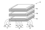
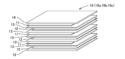
- FIG. 2 is a cross-sectional view taken along the line II-II in FIG. It is a disassembled perspective view of three electrostatic type units 10a, 10b, and 10c. It is a disassembled perspective view of each electrostatic unit 10a, 10b, 10c.
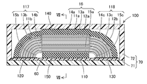
- FIG. 3 is a diagram showing an electrical connection state of the electrostatic laminate 16. It is a section perspective view of electrostatic transducer 1 of a third embodiment. It is VII-VII sectional drawing of FIG.
- the electrostatic transducer 1 is an actuator that uses a change in capacitance and generates vibration or sound, or a sensor that detects vibration or sound.
- the electrostatic transducer 1 as an actuator generates vibration by applying a voltage to the electrodes.
- the electrostatic transducer 1 as a sensor generates a voltage at an electrode when the sensor vibrates due to vibration or sound input.
- the electrostatic transducer 1 as the vibration actuator is, for example, a device that presents tactile vibration to a human, a device that generates vibrations in the opposite phase of the structure for damping the structure, and the like.
- the electrostatic transducer 1 as an actuator that generates sound includes a speaker that generates sound waves felt by human hearing, sound masking that cancels noise noise, and the like.
- the vibration generated by the vibration actuator is relatively low-frequency vibration, and the sound generated by the actuator that generates sound is relatively high-frequency vibration.
- the electrostatic transducer 1 as an actuator in this embodiment is suitable for a low-frequency vibration exciter and a low-frequency sound generator because it uses spring mass vibration.
- the electrostatic transducer 1 will be described with an example of a vibration actuator that presents tactile vibration to humans.
- the electrostatic transducer 1 is applied to an actuator that is mounted on a mobile terminal and vibrates the mobile terminal.
- the electrostatic transducer 1 as a sensor has substantially the same configuration.
- FIGS. 1 to 3 exaggerate the thickness of each member for easy understanding. Therefore, the thickness of the electrostatic transducer 1 in the vertical direction in FIG. 1 is actually very thin.
- the electrostatic transducer 1 includes an electrostatic unit 10 (10a, 10b, 10c), a first conduction part 20, a second conduction part 30, a first elastic body 40, a second The elastic body 50, the control board 60, and the cover 70 are provided.
- the electrostatic unit 10 includes a plurality of stacked electrodes and a plurality of dielectrics.
- the electrostatic transducer 1 may include one electrostatic unit 10 or a plurality of electrostatic units 10.
- the electrostatic transducer 1 includes three electrostatic units 10a, 10b, and 10c, and the three electrostatic units 10a, 10b, and 10c are stacked. It becomes.
- Each electrostatic unit 10a, 10b, 10c is formed in a substantially flat shape (corresponding to a flat shape).
- the outer shape of each of the electrostatic units 10a, 10b, and 10c is formed in a rectangular shape when viewed from the top surface of FIG. 3 (when viewed from the surface normal direction).
- Each electrostatic unit 10a, 10b, 10c is formed of an elastomer.
- each of the electrostatic units 10a, 10b, 10c includes a plurality of first electrode sheets 11, a plurality of second electrode sheets 12, a plurality of dielectric sheets 13, and a surface insulating sheet 14.
- the back insulating sheet 15 is provided and is an integral member of these.
- the electrostatic units 10a, 10b, and 10c are separate members.
- the plurality of first electrode sheets 11 and the plurality of second electrode sheets 12 are formed into a sheet shape from an elastically deformable material, for example, an elastomer.
- the first electrode sheet 11 and the second electrode sheet 12 are formed in the same shape and made of the same material, and the first electrode sheet 11 and the second electrode sheet 12 are formed in a thin film rectangular shape.
- the first electrode sheet 11 and the second electrode sheet 12 are formed by blending a conductive filler in an elastomer. Therefore, the 1st electrode sheet 11 and the 2nd electrode sheet 12 have the property which has flexibility and can be expanded and contracted.
- the elastomer constituting the first electrode sheet 11 and the second electrode sheet 12 include silicone rubber, ethylene-propylene copolymer rubber, natural rubber, styrene-butadiene copolymer rubber, acrylonitrile-butadiene copolymer rubber, acrylic rubber, Epichlorohydrin rubber, chlorosulfonated polyethylene, chlorinated polyethylene, urethane rubber and the like can be applied.
- blended with the 1st electrode sheet 11 and the 2nd electrode sheet 12 should just be the particle
- the plurality of dielectric sheets 13 are formed in a sheet shape from an elastically deformable material, for example, an elastomer.
- the dielectric sheet 13 is formed in a thin film rectangular shape.
- the width in the short direction of the dielectric sheet 13 is formed to be approximately the same as the width in the short direction of the first electrode sheet 11 and the second electrode sheet 12.
- the length of the dielectric sheet 13 in the longitudinal direction is longer than the lengths of the first electrode sheet 11 and the second electrode sheet 12 in the longitudinal direction.
- the dielectric sheet 13 is formed thicker than the first electrode sheet 11 and the second electrode sheet 12.
- the dielectric sheet 13 is formed of an elastomer. Therefore, the dielectric sheet 13 has a flexible and stretchable property.
- a material that functions as a dielectric of the electrostatic transducer 1 is applied to the dielectric sheet 13.
- the dielectric sheet 13 expands and contracts in the thickness direction, and enables expansion and contraction in the flat plane direction along with expansion and contraction in the thickness direction.
- the elastomer constituting the dielectric sheet 13 include silicone rubber, acrylonitrile-butadiene copolymer rubber, acrylic rubber, epichlorohydrin rubber, chlorosulfonated polyethylene, chlorinated polyethylene, and urethane rubber.
- the front insulating sheet 14 and the back insulating sheet 15 are made of an insulating material.
- the front surface insulating sheet 14 and the back surface insulating sheet 15 are formed in the same shape using the same material as that of the dielectric sheet 13. That is, the front surface insulating sheet 14 and the back surface insulating sheet 15 are formed in a rectangular shape from an elastomer.
- the first electrode sheet 11, the dielectric sheet 13, the second electrode sheet 12, the dielectric sheet 13, and the first electrode sheet 11 are laminated in this order.
- the first electrode sheet 11 and the second electrode sheet 12 are offset in the left-right direction (longitudinal direction) in FIG. Specifically, a part of the first electrode sheet 11 and a part of the second electrode sheet 12 are arranged to face each other. And in the 1st electrode sheet 11 and the 2nd electrode sheet 12, the remaining one part which does not mutually oppose is located on the opposite side on the basis of the opposing part.
- the first electrode sheet 11 and the second electrode sheet 12 are opposed to each other at the center portion in the left-right direction, and the first electrode sheet 11 is present on the left side portion, whereas the second electrode sheet is present. 12 does not exist, and in the right side portion, the second electrode sheet 12 exists, whereas the first electrode sheet 11 does not exist.
- the length of the dielectric sheet 13 in the longitudinal direction is a range where the first electrode sheet 11 and the second electrode sheet 12 face each other, a range where only the first electrode sheet 11 exists, and In addition, the length is formed to face the entire range where only the second electrode sheet 12 exists.
- the surface insulating sheet 14 covers one of the outermost layers (the uppermost layer in FIG. 4) of the plurality of first electrode sheets 11 and the plurality of second electrode sheets 12 over the entire surface.
- the back surface insulating sheet 15 covers the other outermost layer (lowermost layer in FIG. 4) of the plurality of first electrode sheets 11 and the plurality of second electrode sheets 12 over the entire surface.
- Each of the electrostatic units 10a, 10b, and 10c includes an electrostatic laminate 16 located at the center in the left-right direction of FIG. 3, a first terminal 17 located on the left side of FIG. 3, and a right side of FIG. And a second terminal 18.
- the first terminal 17 is a ground potential terminal in the electrostatic laminate 16
- the second terminal 18 is a positive potential terminal in the electrostatic laminate 16.
- the first terminal 17 and the second terminal 18 extend on the opposite side with respect to the electrostatic laminate 16.
- the 1st electrode sheet 11 is provided with the 1st counter electrode part 11a located in the center part of a horizontal direction, and the 1st terminal electrode part 11b extended from the 1st counter electrode part 11a.
- the 2nd electrode sheet 12 is provided with the 2nd counter electrode part 12a located in the center part of a horizontal direction, and the 2nd terminal electrode part 12b extended from the 2nd counter electrode part 12a.
- the first counter electrode portion 11a and the second counter electrode portion 12a face each other.
- the direction in which the first terminal electrode portion 11b extends from the first counter electrode portion 11a and the direction in which the second terminal electrode portion 12b extends from the second counter electrode portion 12a are opposite directions.
- the dielectric sheet 13 includes a dielectric body 13a, a first extension portion 13b, and a second extension portion 13c.
- the dielectric body 13a is interposed between the first counter electrode portion 11a and the second counter electrode portion 12a.
- the first extending portion 13b extends from the dielectric body 13a and is interposed between the plurality of first terminal electrode portions 11b.
- the second extending portion 13c extends from the dielectric body 13a and is interposed between the plurality of second terminal electrode portions 12b.
- the surface insulating sheet 14 includes a surface insulating main body 14a, a first surface terminal insulating portion 14b, and a second surface terminal insulating portion 14c.
- the surface insulating body 14a covers the first counter electrode portion 11a located on one of the outermost layers (upper side in FIG. 3).
- the first surface terminal insulating portion 14b covers the first terminal electrode portion 11b located on one of the outermost layers.
- the second surface terminal insulating portion 14c covers the second terminal electrode portion 12b located on one of the outermost layers.
- the back surface insulating sheet 15 includes a back surface insulating main body 15a, a first back surface terminal insulating portion 15b, and a second back surface terminal insulating portion 15c.
- the back insulating main body 15a covers the first counter electrode portion 11a located on the other outermost layer (lower side in FIG. 3).
- the first back terminal insulating portion 15b covers the first terminal electrode portion 11b located on the other outermost layer.
- the second back terminal insulating portion 15c covers the second terminal electrode portion 12b located on the other outermost layer.
- the electrostatic laminate 16 is formed in a planar shape by the plurality of first counter electrode portions 11a, the plurality of second counter electrode portions 12a, the plurality of dielectric bodies 13a, the surface insulating body 14a, and the back surface insulating body 15a. Is done.
- the first terminal 17 is formed in a planar shape by a plurality of first terminal electrode portions 11b, a plurality of first extending portions 13b, a first surface terminal insulating portion 14b, and a first back terminal insulating portion 15b. The first terminal 17 extends in the planar surface direction of the electrostatic laminate 16.
- the second terminal 18 is formed in a planar shape by a plurality of second terminal electrode portions 12b, a plurality of second extending portions 13c, a second surface terminal insulating portion 14c, and a second back surface terminal insulating portion 15c.
- the second terminal 18 extends in the planar surface direction of the electrostatic laminate 16.
- the electrostatic laminate 16 includes all of the constituent members, whereas the first terminal 17 does not include the second electrode sheet 12, and the second terminal 18 does not include the first electrode sheet 11. Not equipped. Therefore, the thickness of the first terminal 17 and the second terminal 18 is thinner than that of the electrostatic laminate 16. However, the thickness of the first electrode sheet 11 and the second electrode sheet 12 is very thin. In particular, the thicknesses of the first electrode sheet 11 and the second electrode sheet 12 are very thin compared to the dielectric sheet 13. Therefore, the difference between the thickness of the electrostatic laminate 16 and the thickness of the first terminal 17 and the difference between the thickness of the electrostatic laminate 16 and the thickness of the second terminal 18 are not so large.
- the bending in the boundary part of the 1st counter electrode part 11a and the 1st terminal electrode part 11b is small.
- the bending at the boundary portion between the second counter electrode portion 12a and the second terminal electrode portion 12b is small.
- each electrostatic unit 10a, 10b, 10c is formed independently, in each electrostatic unit 10a, 10b, 10c, the thickness of the electrostatic laminate 16 and The difference in the thickness of the first terminal 17 and the difference in the thickness of the electrostatic laminate 16 and the thickness of the second terminal 18 are not so large. Also from this, in the 1st electrode sheet 11, the bending in the boundary part of the 1st counter electrode part 11a and the 1st terminal electrode part 11b is small. Furthermore, the bending at the boundary portion between the second counter electrode portion 12a and the second terminal electrode portion 12b is small.
- the first conduction portion 20 is formed in a sheet shape from an elastically deformable material (for example, elastomer), and is bent in an L shape.
- electrical_connection part 20 is shape
- FIG. However, the thickness of the 1st conduction
- One side of the L-shape of the first conduction part 20 is formed in a direction intersecting (orthogonal to) the planar surface of the electrostatic laminate 16.
- One side of the L shape of the first conduction part 20 is in contact with the end face of the first terminal 17.
- one side of the L shape of the first conducting portion 20 is in contact with the end of the first terminal electrode portion 11b and the end of the first extending portion 13b. Therefore, the 1st conduction
- the other side of the L-shape of the first conductive portion 20 extends in a direction away from the electrostatic laminate 16 and is formed in parallel to the planar surface direction of the electrostatic laminate 16.
- the other side of the L shape of the first conduction part 20 is electrically connected to a control board 60 described later.
- the second conducting portion 30 is formed in a sheet shape from an elastically deformable material (for example, an elastomer) and bent into an L shape, similarly to the first conducting portion 20.
- electrical_connection part 30 is shape
- One side of the L-shape of the second conducting portion 30 is formed in a direction intersecting (orthogonal to) the planar surface of the electrostatic laminate 16. Then, one side of the L shape of the second conducting portion 30 is in contact with the end face of the second terminal 18. Specifically, one side of the L shape of the second conducting portion 30 is in contact with the end of the second terminal electrode portion 12b and the end of the second extending portion 13c. Accordingly, the second conduction portion 30 is electrically connected to the ends of the plurality of second terminal electrode portions 12b.
- the other L-shaped side of the second conducting portion 30 extends in a direction away from the electrostatic laminate 16 and is formed in parallel to the planar surface direction of the electrostatic laminate 16.
- the other side of the L shape of the second conducting portion 30 is electrically connected to a control board 60 described later.
- the first elastic body 40 is disposed in contact with one planar surface of the electrostatic laminate 16.
- the second elastic body 50 is disposed in contact with the other planar surface of the electrostatic laminate 16. That is, the first elastic body 40 and the second elastic body 50 are respectively disposed on both end faces (upper and lower surfaces in FIG. 1) facing away from each other in the planar surface orthogonal direction of the electrostatic laminate 16.
- the first elastic body 40 has both end surfaces facing away from each other in the planar surface direction of the electrostatic laminate 16 (surfaces on which the first terminal 17 and the second terminal 18 do not exist (see FIG. 2). 2 in contact with the left and right side surfaces)). Furthermore, as shown in FIG. 1, the first elastic body 40 includes one planar surface of the first terminal 17 (upper surface in FIG. 1) and a planar one surface of the second terminal 18 (upper surface in FIG. 1). ) Is placed in contact with. The second elastic body 50 is disposed in contact with the other planar surface of the first terminal 17 (lower surface in FIG. 1) and the other planar surface of the second terminal 18 (lower surface in FIG. 1).
- first elastic body 40 is arranged in contact with all the L-shaped outer surfaces of the first conducting portion 20 and all the L-shaped outer surfaces of the second conducting portion 30.
- the surface of the second elastic body 50 opposite to the electrostatic laminate 16 is formed so as to be substantially flush with the other L-shaped surfaces of the first conductive portion 20 and the second conductive portion 30.
- the first elastic body 40 and the second elastic body 50 are made of materials having small elastic moduli E (40) and E (50) and small loss coefficients tan ⁇ (40) and tan ⁇ (50) .
- the first elastic body 40 and the second elastic body 50 are preferably made of a soft material having low damping characteristics.
- the first elastic body 40 and the second elastic body 50 have elastic moduli E (40) and E ( 40) that are smaller than the elastic modulus E1 (16) in the stacking direction (planar plane orthogonal direction) of the electrostatic laminate 16. 50) have.
- the elastic modulus E (40) of the first elastic body 40 is smaller than the elastic modulus E2 (16) in the surface direction of the electrostatic laminate 16.
- the ratio of the elastic modulus E (40) of the first elastic body 40 to the elastic modulus E1 (16) in the stacking direction of the electrostatic laminate 16 is 15% or less.
- the ratio of the elastic modulus E (50) of the second elastic body 50 to the elastic modulus E1 (16) in the stacking direction of the electrostatic laminate 16 is 15% or less. These ratios are preferably 10% or less.
- the ratio of the elastic modulus E (40) of the first elastic body 40 to the elastic modulus E2 (16) in the surface direction of the electrostatic laminate 16 is 15% or less.
- the ratio of the elastic modulus E (50) of the second elastic body 50 to the elastic modulus E2 (16) in the surface direction of the electrostatic laminate 16 is 15% or less. These ratios are preferably 10% or less.
- first elastic body 40 and the second elastic body 50 have loss coefficients tan ⁇ (40) and tan ⁇ (50) equal to or less than the loss coefficient tan ⁇ (16) of the electrostatic laminate 16 under predetermined conditions.
- the predetermined condition means a use environment where the temperature is ⁇ 10 to 50 ° C. and the vibration frequency is 300 Hz or less.
- silicone rubber is suitable for the first elastic body 40 and the second elastic body 50.
- urethane rubber is better suited to the first elastic body 40 and the second elastic body 50 than urethane rubber because urethane rubber has better damping characteristics than silicone rubber.
- urethane rubber may be used for the first elastic body 40 and the second elastic body 50 depending on the intended characteristics.
- the control board 60 is disposed in parallel to the electrostatic laminate 16 and is disposed in contact with the surface of the second elastic body 50 opposite to the electrostatic laminate 16. Furthermore, the control board 60 is in contact with the other L-shaped surfaces of the first conduction part 20 and the second conduction part 30.
- the cover 70 surrounds the electrostatic unit 10, the first conduction part 20, the second conduction part 30, the first elastic body 40, the second elastic body 50, and the control board 60.
- Various materials such as metal and resin are applied to the cover 70, for example.
- the cover 70 includes a planar first cover 71 for fixing the control board 60 and a second cover 72 attached to the first cover 71.
- the first cover 71 and the second cover 72 hold the electrostatic laminate 16, the first elastic body 40, and the second elastic body 50 in a compressed state in the stacking direction of the electrostatic laminate 16. In this state, the first elastic body 40 and the second elastic body 50 are more compressed than the electrostatic laminate 16 in the stacking direction of the electrostatic laminate 16 from the relationship of the elastic modulus E of each member. It becomes.
- the first cover 71 holds the electrostatic laminate 16 and the first elastic body 40 in a compressed state in the surface direction of the electrostatic laminate 16. In this state, from the relationship of the elastic modulus E of each member, the first elastic body 40 is compressed more than the electrostatic laminate 16 in the surface direction of the electrostatic laminate 16.
- FIG. 5 shows one electrostatic cell constituting the electrostatic laminate 16.
- the electrostatic cell is one first counter electrode portion 11a, one second counter electrode portion 12a, and one dielectric body 13a.
- the first counter electrode part 11 a and the second counter electrode part 12 a are arranged to face each other with a distance in the stacking direction of the electrostatic laminate 16.
- the other terminal that supplies a periodic voltage is electrically connected to the first counter electrode portion 11 a by a drive circuit in the control board 60.
- One terminal for supplying a periodic voltage is electrically connected to the second counter electrode portion 12a.
- the first counter electrode portion 11a is connected to the ground potential.
- the second counter electrode portion 12 a is connected to the output terminal of the control board 60.
- a periodic voltage is applied to the first counter electrode part 11a and the second counter electrode part 12a via the first terminal electrode part 11b and the second terminal electrode part 12b.
- the periodic voltage may be an AC voltage (periodic voltage including positive and negative) or a periodic voltage offset to a positive value.
- the dielectric body 13a When the charge accumulated in the first counter electrode portion 11a and the second counter electrode portion 12a increases, the dielectric body 13a is compressed and deformed. That is, as shown in FIG. 5, the thickness of the electrostatic laminate 16 is reduced, and the size (width and depth) in the surface direction of the electrostatic laminate 16 is increased. Conversely, when the charge accumulated in the first counter electrode portion 11a and the second counter electrode portion 12a decreases, the dielectric body 13a returns to its original thickness. That is, the thickness of the electrostatic laminate 16 is increased, and the size in the surface direction of the electrostatic laminate 16 is decreased. Thus, the electrostatic laminate 16 expands and contracts in the stacking direction and expands and contracts in the surface direction.
- the electrostatic transducer 1 When the electrostatic laminate 16 performs an expansion / contraction operation, the electrostatic transducer 1 operates as follows. As shown in FIG. 1, the electrostatic transducer 1 has a state where the first elastic body 40 and the second elastic body 50 are compressed as an initial state. Accordingly, when the thickness of the electrostatic laminate 16 is reduced due to an increase in charge, the first elastic body 40 and the second elastic body 50 are deformed so that the amount of compression is smaller than the initial state. On the other hand, when the thickness of the electrostatic laminate 16 increases due to the decrease in charge, the first elastic body 40 and the second elastic body 50 operate so as to return to the initial state. That is, the first elastic body 40 and the second elastic body 50 are deformed so that the amount of compression becomes larger than in the case of an increase in charge.
- the above operation is repeated. Then, the state where the center of the electrostatic laminate 16 is concave toward the second elastic body 50 and the state where the center of the electrostatic laminate 16 is convex toward the second elastic body 50 are repeated. Since the electrostatic laminate 16 is regulated by the cover 70 via the first elastic body 40 and the second elastic body 50, the above operation is performed.
- the displacement in the stacking direction of the electrostatic laminate 16 (the same direction as the d33 direction electric field) is transmitted to the cover 70 via the first elastic body 40.
- the elastic deformation force of the first elastic body 40 is changed by the expansion / contraction operation of the electrostatic laminate 16.
- a change in elastic deformation force of the first elastic body 40 is transmitted to the cover 70. Therefore, by virtue of the compression of the first elastic body 40 and the second elastic body 50 as an initial state, vibration in the stacking direction (d33 direction) of the electrostatic laminate 16 can be efficiently applied to the cover 70. Can do. That is, tactile vibration can be applied to the cover 70 even if the electrostatic laminate 16 is a small vibration.
- the displacement in the surface direction of the electrostatic laminate 16 (d31 direction: direction orthogonal to the electric field) is applied to the cover 70 via the first elastic body 40. Communicated.
- vibration in the surface direction (d31 direction) of the electrostatic laminate 16 is applied to the cover 70.
- the vibration in the surface direction (d31 direction) of the electrostatic laminate 16 is smaller than the vibration in the lamination direction (d33 direction).
- a large tactile vibration can be applied to the entire cover 70 by applying a vibration in the plane direction (d31) to the vibration in the stacking direction (d33 direction) of the electrostatic laminate 16.
- the loss coefficients tan ⁇ (40) and tan ⁇ (50) of the first elastic body 40 and the second elastic body 50 are very large, even if the electrostatic laminate 16 performs an expansion / contraction operation, Vibrations are absorbed by the first elastic body 40 and the second elastic body 50. In this case, even if the electrostatic laminate 16 performs an expansion / contraction operation, it is not transmitted to the cover 70.
- the first elastic body 40 and the second elastic body 50 use materials having small loss coefficients tan ⁇ (40) and tan ⁇ (50) . Therefore, vibration due to the expansion and contraction operation of the electrostatic laminate 16 is transmitted to the cover 70 while being hardly absorbed by the first elastic body 40 and the second elastic body 50.
- the elastic moduli E (40) and E (50) of the first elastic body 40 and the second elastic body 50 are smaller than the elastic modulus E1 (16) in the stacking direction of the electrostatic laminate 16. Therefore, in the initial state in which no voltage is applied to the first counter electrode part 11a and the second counter electrode part 12a, the electrostatic laminate 16 is almost not compressed. Therefore, even if the cover 70 presses the electrostatic stack 16 in the stacking direction, the expansion / contraction operation of the electrostatic stack 16 in the stacking direction is not affected. That is, the electrostatic laminate 16 can reliably perform an expansion / contraction operation.
- the elastic modulus E (40) of the first elastic body 40 is smaller than the elastic modulus E2 (16) in the surface direction of the electrostatic laminate 16. Therefore, in the initial state in which no voltage is applied to the first counter electrode part 11a and the second counter electrode part 12a, the electrostatic laminate 16 is almost not compressed. Therefore, even if the cover 70 presses the electrostatic laminate 16 in the surface direction, the expansion / contraction operation in the surface direction of the electrostatic laminate 16 is not affected. That is, the electrostatic laminate 16 can reliably perform an expansion / contraction operation.
- the first elastic body 40 may be disposed only on the end surface in the direction perpendicular to the plane of the electrostatic laminate 16. In this case, the first elastic body 40 is not disposed on the end surface in the surface direction of the electrostatic laminate 16. Accordingly, the electrostatic transducer 1 does not apply vibration in the surface direction (d31 direction) of the electrostatic laminate 16 to the cover 70.
- the outermost layer of the electrostatic laminate 16 is formed so that the elastic modulus in the lamination direction is larger than that of the other layers.
- the outermost layer of the electrostatic laminate 16 is the uppermost layer of the electrostatic unit 10a in FIG. 3 and the lowermost layer of the electrostatic unit 10c in FIG.
- a nano-order cured layer is formed on the uppermost layer of the electrostatic unit 10a by surface modification by UV irradiation.
- a nano-order cured layer is formed on the lowermost layer of the electrostatic unit 10c by surface modification by UV irradiation.
- a sheet having a desired elastic modulus may be disposed.
- the electrostatic transducer 100 includes an electrostatic unit 110, a first conduction part 120, a second conduction part 130, a first elastic body 140, a second elastic body 150, a control board 60, and a cover 70.
- the electrostatic unit 110 includes an electrostatic laminate 16, a first terminal 117, and a second terminal 118.
- the electrostatic laminate 16 is formed in a planar shape.
- the electrostatic laminate 16 is formed by a first counter electrode portion 11a, a second counter electrode portion 12a, and a dielectric body 13a. That is, the 1st counter electrode part 11a, the 2nd counter electrode part 12a, and the dielectric main body 13a are formed in planar shape.
- the first terminal 117 is formed to be bent from the plane surface direction of the electrostatic laminate 16.
- the first terminal 117 is formed in an arc shape of about 90 degrees.
- the 1st terminal 117 is formed of the 1st terminal electrode part 11b and the 1st extension part 13b. That is, the first terminal electrode portion 11b and the first extension portion 13b are bent and formed in a curved shape.
- the second terminal 118 is formed to be bent from the planar surface direction of the electrostatic laminate 16.
- the second terminal 118 is formed in an arc shape of about 90 degrees.
- the 2nd terminal 118 is formed of the 2nd terminal electrode part 12b and the 2nd extension part 13c. That is, the second terminal electrode portion 12b and the second extending portion 13c are bent and formed in a curved shape.
- the first conducting part 120 and the second conducting part 130 are formed in a planar sheet shape.
- the first conduction portion 120 and the second conduction portion 130 are in contact with the ends of the first terminal 117 and the second terminal 118, respectively. Further, the first conduction part 120 and the second conduction part 130 are formed in parallel to the planar surface direction of the electrostatic laminate 16.
- the first conduction unit 120 and the second conduction unit 130 are electrically connected to the control board 60.
- the first elastic body 140 is arranged in contact with one planar surface of the electrostatic laminate 16 (upper surface in FIGS. 6 and 7). Further, as shown in FIG. 7, the first elastic body 140 is disposed in contact with both end faces (left and right faces in FIG. 7) facing away from the planar surface direction of the electrostatic laminate 16. Further, as shown in FIG. 6, the first elastic body 140 is disposed in contact with the curved convex surface of the first terminal 117 and the curved convex surface of the second terminal 118. Although not shown, the first elastic body 140 is arranged in contact with the side surface of the first terminal 117 (front and rear surfaces in FIG. 6) and the side surface of the second terminal 118 (front and rear surfaces in FIG. 6). It may be.
- the second elastic body 150 is disposed in contact with the other planar surface (the lower surface in FIGS. 6 and 7) of the electrostatic laminate 16.
- the second elastic body 150 is not in contact with the curved concave surface of the first terminal 117 and the curved concave surface of the second terminal 118, but may be arranged in contact with the curved concave surface.
- the electrostatic transducers 1, 100 of the first, second, and third embodiments include a plurality of first electrode sheets 11 formed into a sheet shape by an elastically deformable material, and a sheet shape from an elastically deformable material.
- Each of the plurality of first electrode sheets 11 includes a first counter electrode portion 11a and a first terminal electrode portion 11b extending from the first counter electrode portion 11a.
- Each of the plurality of second electrode sheets 12 includes a second counter electrode portion 12a facing the first counter electrode portion 11a and a second terminal electrode portion 12b extending from the second counter electrode portion 12a.
- Each of the plurality of dielectric sheets 13 includes a dielectric body 13a interposed between the first counter electrode portion 11a and the second counter electrode portion 12a, and extends from the dielectric body 13a and a plurality of first terminals.
- a first extending portion 13b interposed between the electrode portions 11b and a second extending portion 13c extending from the dielectric body 13a and interposed between the plurality of second terminal electrode portions 12b are provided.
- first counter electrode portion 11 a and the first terminal electrode portion 11 b are the same first electrode sheet 11.
- second counter electrode portion 12a and the second terminal electrode portion 12b are the same second electrode sheet 12.
- the first electrode sheet 11 and the second electrode sheet 12 can be formed very thin. That is, the electrostatic laminate 16 including the first counter electrode portion 11a, the second counter electrode portion 12a, and the dielectric body 13a has a small and large capacitance.
- the 1st electrode sheet 11 is provided with the 1st counter electrode part 11a and the 1st terminal electrode part 11b.
- the first terminal electrode portion 11b exists outside the electrostatic laminate 16 as a configuration of the conductive path connected to the first counter electrode portion 11a.
- the first terminal electrode portion 11 b is extremely thin compared to the electrostatic laminate 16. Therefore, if only the first terminal electrode part 11b is present outside the electrostatic laminate 16 as a part for extracting electricity from the first counter electrode part 11a, the first terminal electrode part 11b and the first A large deformation force is received near the boundary with the counter electrode portion 11a.
- the first terminal electrode portion 11b alone is not present outside the electrostatic laminate 16 but is a part of the dielectric sheet 13.
- the extending portion 13b is made to exist outside the electrostatic laminate 16, and the first terminal electrode portion 11b and the first extending portion 13b are stacked. Therefore, the total thickness of the first terminal electrode part 11 b and the first extension part 13 b is only a thickness of the second electrode sheet 12 that is smaller than that of the electrostatic laminate 16. Therefore, it is possible to suppress a large deformation force from being generated near the boundary between the first terminal electrode portion 11b and the first counter electrode portion 11a. As a result, the constituent portion of the conductive path connected to the first counter electrode portion 11a can have high durability. The same applies to the second terminal electrode portion 12b.
- the dielectric sheet 13 is not only between the first counter electrode portion 11a and the second counter electrode portion 12a, but also between the first terminal electrode portions 11b and between the second terminal electrode portions 12b. It is also placed in between.
- the size of the electrostatic capacitance of the electrostatic transducer 1 is such that the first extending portion 13b that exists between the first terminal electrode portions 11b in the dielectric sheet 13 and the second terminal electrode portion 12b.
- the 2nd extension part 13c which exists in is an unnecessary part.
- the first terminal electrode portion 11b and the second terminal electrode are provided by intentionally presenting the first extending portion 13b and the second extending portion 13c that do not contribute to the capacitance. The durability of the portion 12b can be improved.
- the first terminal electrode portion 11b extends from the first counter electrode portion 11a
- the second terminal electrode portion 12b extends from the second counter electrode portion 12a.
- the direction is the opposite direction. That is, the first terminal 17 formed by the first terminal electrode part 11b and the first extension part 13b and the second terminal 18 formed by the second terminal electrode part 12b and the second extension part 13c are It is suitable.
- the peripheral surface peripheral surface around the surface normal
- the surfaces adjacent to the first terminal 17 and the second terminal 18 (the left and right surfaces in FIGS. 2 and 7) To do. Accordingly, the deformation of the electrostatic laminate 16 and conversion between electricity can be performed on the adjacent surfaces.
- the electrostatic transducer 1 includes a first conduction unit 20 and a second conduction unit 30.
- the first conduction portion 20 is formed of an elastically deformable material, contacts the end of the first terminal electrode portion 11b and the end of the first extension portion 13b, and is connected to the ends of the plurality of first terminal electrode portions 11b. Electrically connected.
- the second conducting portion 30 is formed of an elastically deformable material, is in contact with the end of the second terminal electrode portion 12b and the end of the second extending portion 13c, and is connected to the ends of the plurality of second terminal electrode portions 12b. Electrically connected.
- the first conductive portion 20 can easily form a conductive path between the plurality of first terminal electrode portions 11b.
- the second conductive portion 30 can easily form a conductive path between the plurality of second terminal electrode portions 12b.
- electrical_connection part 30 are elastically deformable, it can track the deformation
- the electrostatic laminate 16 including the first counter electrode portion 11a, the second counter electrode portion 12a, and the dielectric body 13a is formed in a planar shape.
- the first terminal electrode portion 11 b, the second terminal electrode portion 12 b, the first extension portion 13 b, and the second extension portion 13 c extend in the planar surface direction of the electrostatic laminate 16. Thereby, it can suppress that a big deformation force arises in the boundary vicinity of the 1st terminal electrode part 11b and the 1st counter electrode part 11a.
- the component for extracting electricity from the first counter electrode portion 11a can have high durability.
- the electrostatic laminate 16 including the first counter electrode portion 11a, the second counter electrode portion 12a, and the dielectric body 13a is formed in a planar shape.
- the first terminal electrode portion 11 b, the second terminal electrode portion 12 b, the first extension portion 13 b, and the second extension portion 13 c extend in the planar surface direction of the electrostatic laminate 16.
- electrical_connection part 30 are formed in the direction which cross
- the electrostatic transducer 1 includes a plurality of stacked electrostatic units 10a, 10b, and 10c.
- Each of the electrostatic units 10a, 10b, and 10c is formed by using the first electrode sheet 11, the second electrode sheet 12, and the dielectric sheet 13 as an integral member.
- electrical_connection part 20 is electrically connected to the some 1st terminal electrode part 11b in the some electrostatic type units 10a, 10b, and 10c.
- electrical_connection part 30 is electrically connected to the some 2nd terminal electrode part 12b in the some electrostatic type units 10a, 10b, and 10c.
- each electrostatic type unit 10a, 10b, 10c it can suppress that big deformation force arises in the boundary vicinity of the 1st terminal electrode part 11b and the 1st counter electrode part 11a. The same applies to the second terminal electrode portion 12b.
- the electrostatic laminate 16 including the first counter electrode portion 11a, the second counter electrode portion 12a, and the dielectric body 13a is formed in a planar shape.
- the first terminal electrode portion 11b and the first extension portion 13b are formed to be bent from a planar surface direction in the electrostatic laminate 16.
- the second terminal electrode portion 12b and the second extending portion 13c are formed to be bent from the planar surface direction.
- the first terminal 17 is bent and formed so as to be large in the vicinity of the boundary between the first terminal electrode portion 11b and the first counter electrode portion 11a. Generation of deformation force can be suppressed. The same applies to the second terminal 18.
- the electrostatic laminate 16 composed of the first counter electrode portion 11a, the second counter electrode portion 12a, and the dielectric body 13a is formed in a planar shape.
- the first terminal electrode portion 11b and the first extension portion 13b are formed to be bent from a planar surface direction in the electrostatic laminate 16.
- the second terminal electrode portion 12 b and the second extending portion 13 c are formed to be bent from a planar surface direction in the electrostatic laminate 16.
- the first conductive portion 20 and the second conductive portion 30 are formed in parallel to the planar surface direction of the electrostatic laminate 16. Thereby, it becomes easy to form the electrostatic transducer 1 in a flat shape as a whole.
- the electrostatic transducer 1 is an insulating sheet that covers the outermost layer of the plurality of first electrode sheets 11 and the plurality of second electrode sheets 12 over the entire surface. 14 and 15 are further provided. As a result, the insulating coating on the electrostatic laminate 16, the insulating coating on the first terminal 17, and the insulating coating on the second terminal 18 can be made very simple.
- the electrostatic laminated body 16 comprised by the 1st counter electrode part 11a, the 2nd counter electrode part 12a, and the dielectric main body 13a is formed in planar shape.
- the electrostatic transducer 1 is arranged on each of both end faces (upper and lower surfaces in FIG. 1) facing away from each other in the planar plane orthogonal direction (surface normal direction) in the electrostatic laminate 16. , 50.
- the electrostatic transducer 1 includes a cover 70 that presses the electrostatic laminate 16 in the laminating direction and holds the elastic bodies 40 and 50 in a state of being compressed more than the electrostatic laminate 16. Thereby, in the stacking direction of the electrostatic laminate 16, even if the electrostatic laminate 16 itself is a small vibration, a large vibration can be applied to the cover 70.
- the elastic body 40 has both end surfaces (upper and lower surfaces in FIG. 1) facing away from each other in the planar surface orthogonal direction (surface normal direction) in the electrostatic laminate 16. ) And both end surfaces (left and right surfaces in FIG. 1) facing away from each other in the planar surface direction of the electrostatic laminate 16.
- the cover 70 is pressed in the surface direction of the electrostatic laminate 16 and holds the elastic body 40 in a state of being compressed more than the electrostatic laminate 16. Thereby, the vibration in the surface direction of the electrostatic laminate 16 can be used. In both the stacking direction and the surface direction, even if the electrostatic laminate 16 is a small vibration, a large vibration can be applied to the cover 70.
- the elastic moduli E (40) and E (50) of the elastic bodies 40 and 50 are smaller than the elastic moduli E1 (16) and E2 (16) of the electrostatic laminate 16. That is, in the initial state, when the electrostatic laminate 16 and the elastic bodies 40 and 50 are pressed by the cover 70, the compression amount of the electrostatic laminate 16 is small. Therefore, even if the electrostatic laminate 16 is pressed by the cover 70, the expansion / contraction operation of the electrostatic laminate 16 is not significantly affected.
- the electrostatic laminate 16 expands and contracts in the stacking direction and the plane direction.
- the displacement of the surface of the electrostatic laminate 16 caused by the expansion / contraction operation of the electrostatic laminate 16 is transmitted to the cover 70 via the elastic bodies 40 and 50.
- the elastic deformation force of the elastic bodies 40 and 50 is changed by the expansion and contraction operation of the electrostatic laminate 16, and the change in the elastic deformation force of the elastic bodies 40 and 50 is transmitted to the cover 70. Therefore, as the initial state, the elastic bodies 40 and 50 are compressed, so that the cover 70 can be efficiently vibrated. That is, tactile vibration can be applied to the cover 70 even if the electrostatic laminate 16 is a small vibration.
- the elastic bodies 40 and 50 are made of a material having small loss coefficients tan ⁇ (40) and tan ⁇ (50) . Thereby, the elastic bodies 40 and 50 can transmit to the cover 70, without absorbing the vibration by the expansion-contraction operation
- the loss coefficients tan ⁇ (40) and tan ⁇ (50) of the elastic bodies 40 and 50 are equal to or less than the loss coefficient tan ⁇ (16) of the electrostatic laminate 16 under a predetermined condition.
- the predetermined condition is a use environment in which the temperature is ⁇ 10 to 50 ° C. and the vibration frequency is 300 Hz or less.
- the outermost layer of the electrostatic laminate 16 including the first counter electrode portion 11a, the second counter electrode portion 12a, and the dielectric body 13a is more elastic in the stacking direction than the other layers. It is formed to increase the rate. Thereby, vibration due to the expansion and contraction operation of the electrostatic laminate 16 is more efficiently transmitted to the cover 70.
- the outermost layer of the electrostatic laminate 16 is preferably a layer whose surface has been modified by UV irradiation.
- the outermost layer can have a very thin thickness on the nano order.
- the transmission efficiency of the vibration by the expansion / contraction operation can be improved without hindering the expansion / contraction operation itself of the electrostatic laminate 16.
- Electrostatic transducer 10, 10a, 10b, 10c, 110: Electrostatic unit, 11: First electrode sheet, 11a: First counter electrode part, 11b: First terminal electrode part, 12: No. Two-electrode sheet, 12a: second counter electrode part, 12b: second terminal electrode part, 13: dielectric sheet, 13a: dielectric body, 13b: first extension part, 13c: second extension part, 14: Surface insulating sheet, 14a: surface insulating body, 14b: first surface terminal insulating part, 14c: second surface terminal insulating part, 15: back surface insulating sheet, 15a: back surface insulating body, 15b: first back surface terminal insulating part, 15c : Second back terminal insulating part, 16: electrostatic laminate, 17, 117: first terminal, 18, 118: second terminal, 20, 120: first conducting part, 30, 130: Two conductive portions, 40, 140: first elastic members, 50, 150: second elastic body, 60: control board, 70: Cover
Landscapes
- Engineering & Computer Science (AREA)
- Physics & Mathematics (AREA)
- Acoustics & Sound (AREA)
- Signal Processing (AREA)
- Mechanical Engineering (AREA)
- Electrostatic, Electromagnetic, Magneto- Strictive, And Variable-Resistance Transducers (AREA)
Abstract
小型かつ大きな静電容量を有すると共に、電極に接続される導電経路の構成部位に耐久性を有することができる静電型トランスデューサ(1)を提供する。静電型トランスデューサ(1)は、複数の第一電極シート(11)と、複数の第二電極シート(12)と、複数の誘電体シート(13)とを備える。複数の第一電極シート(11)のそれぞれは、第一対向電極部(11a)と、第一端子電極部(11b)とを備える。複数の第二電極シート(12)のそれぞれは、第二対向電極部(12a)と、第二端子電極部(12b)とを備える。複数の誘電体シート(13)のそれぞれは、誘電体本体(13a)と、複数の第一端子電極部(11b)の間に介在される第一延在部(13b)と、複数の第二端子電極部(12b)の間に介在される第二延在部(13c)とを備える。
Description
本発明は、静電型トランスデューサに関するものである。
静電型トランスデューサは、静電容量の変化を利用しており、振動や音などを発生させるアクチュエータ、または、振動や音などを検出するセンサである。特開2014-150600号公報には、複数の電極被覆体を1層ごとに交互にずらして積層させたアクチュエータが記載されている。これにより、電極間の沿面放電が防止されるとされている。また、それぞれの電極被覆体を構成する電極層は、電源電極に接続されている。
また、特公昭63-10594号公報及び特開2005-312230号公報には、圧電素子を用いた装置が記載されている。特公昭63-10594号公報に記載の装置では、上下面に電極薄膜が形成された圧電素子を交互に上下面を逆にして多数積層され、各電極薄膜をそれぞれ共通接続するように側面電極が形成されている。特開2005-312230号公報に記載の装置では、接続電極がそれぞれロール体の両端面に配置されている構成が記載されている。
静電型トランスデューサは、小型で、且つ、大きな静電容量を有することが望まれる。大きな静電容量を確保するために多数の電極層と誘電層とを積層する場合において、電極層の厚みを薄くすることにより、小型で且つ大きな静電容量を有するトランスデューサとすることができる。しかし、特開2014-150600号公報に記載の静電型アクチュエータでは、電極層を有する電極被覆体を薄くすることが困難であり、当該電極被覆体を多数積層すると、アクチュエータ全体が大型となる。
また、電極層の厚みを薄くした場合に、各電極層から電気を取り出すため端子の構成をどのようにするかが問題となる。特に、電極層は、薄いため、電極層を延長して端子を構成したとすると、電極層の耐久性が問題となる。特に、静電型トランスデューサの誘電体が変形するため、端子としての電極層の部分が誘電体の変形に追従できることが求められる。
本発明は、小型かつ大きな静電容量を有すると共に、電極に接続される導電経路の構成部位に耐久性を有することができる静電型トランスデューサを提供することを目的とする。
本発明に係る静電型トランスデューサは、弾性変形可能な材料によりシート状に形成される複数の第一電極シートと、弾性変形可能な材料によりシート状に形成される複数の第二電極シートと、弾性変形可能な材料によりシート状に形成される複数の誘電体シートとを備える。
前記複数の第一電極シートのそれぞれは、第一対向電極部と、前記第一対向電極部から延在する第一端子電極部とを備える。前記複数の第二電極シートのそれぞれは、前記第一対向電極部に対向する第二対向電極部と、前記第二対向電極部から延在する第二端子電極部とを備える。
前記複数の誘電体シートのそれぞれは、前記第一対向電極部と前記第二対向電極部との間に介在される誘電体本体と、前記誘電体本体から延在すると共に複数の前記第一端子電極部の間に介在される第一延在部と、前記誘電体本体から延在すると共に複数の前記第二端子電極部の間に介在される第二延在部とを備える。
つまり、第一対向電極部と第一端子電極部とは、同一の第一電極シートである。同様に、第二対向電極部と第二端子電極部とは、同一の第二電極シートである。第一電極シートおよび第二電極シートは、非常に薄く形成することができる。つまり、第一対向電極部、第二対向電極部および誘電体本体により構成される静電型積層体は、小型かつ大きな静電容量を有する。
ここで、第一電極シートが、第一対向電極部と第一端子電極部とを備える。例えば、第一対向電極部に接続される導電経路の構成として、第一端子電極部のみを静電型積層体の外部に存在させることが考えられる。しかし、第一端子電極部は、静電型積層体に比べると、極めて薄い。そのため、仮に、第一対向電極部から電気を取り出す部位として、第一端子電極部のみを静電型積層体の外部に存在させた場合には、第一端子電極部と第一対向電極部との境界付近に大きな変形力を受けてしまう。
しかし、本発明によれば、第一端子電極部のみを静電型積層体の外部に存在させるのではなく、誘電体シートの一部である第一延在部を静電型積層体の外部に存在させることとし、第一端子電極部と第一延在部とを積層している。従って、第一端子電極部と第一延在部との合計厚みは、静電型積層体に比べて第二電極シートの厚み分が薄くなるだけである。そのため、第一端子電極部と第一対向電極部との境界付近に大きな変形力が生じることを抑制できる。その結果、第一対向電極部に接続される導電経路の構成部位が高い耐久性を有することができる。第二端子電極部についても同様である。
上述したように、誘電体シートは、第一対向電極部と第二対向電極部の間のみならず、第一端子電極部同士の間、および、第二端子電極部同士の間にも配置されている。静電型トランスデューサの静電容量の大きさには、誘電体シートにおける第一端子電極部同士の間に存在する第一延在部、および、第二端子電極部同士の間に存在する第二延在部は、不要な部分である。しかし、静電容量の大きさには寄与しない部分である第一延在部および第二延在部をあえて存在させることにより、上記のとおり、第一端子電極部および第二端子電極部の耐久性を向上することができる。
<1.第一実施形態>
(1-1.静電型トランスデューサ1の概要)
静電型トランスデューサ1は、静電容量の変化を利用しており、振動や音などを発生させるアクチュエータ、または、振動や音などを検出するセンサである。アクチュエータとしての静電型トランスデューサ1は、電極に電圧を印加することにより振動を発生する。センサとしての静電型トランスデューサ1は、振動や音の入力に起因してセンサが振動することで電極に電圧を発生する。
(1-1.静電型トランスデューサ1の概要)
静電型トランスデューサ1は、静電容量の変化を利用しており、振動や音などを発生させるアクチュエータ、または、振動や音などを検出するセンサである。アクチュエータとしての静電型トランスデューサ1は、電極に電圧を印加することにより振動を発生する。センサとしての静電型トランスデューサ1は、振動や音の入力に起因してセンサが振動することで電極に電圧を発生する。
加振アクチュエータとしての静電型トランスデューサ1は、例えば、人間に触覚振動を提示する装置、構造物の制振のために構造物の逆位相の振動を発生する装置などである。音を発生するアクチュエータとしての静電型トランスデューサ1は、人間の聴覚にて感じる音波を発生するスピーカ、ノイズ音をキャンセルするサウンドマスキングなどである。
加振アクチュエータが発生する振動は、相対的に低周波振動であり、音を発生するアクチュエータが発生する音は、相対的に高周波振動である。本実施形態におけるアクチュエータとしての静電型トランスデューサ1は、バネマス系の振動を利用するため、低周波振動の加振器、および、低周波音の発生器に適している。
本実施形態においては、静電型トランスデューサ1は、人間に触覚振動を提示する加振アクチュエータを例に挙げて説明する。例えば、静電型トランスデューサ1は、携帯端末に搭載して、携帯端末を振動させるアクチュエータに適用される。なお、センサとしての静電型トランスデューサ1についても、実質的に同様の構成となる。
(1-2.静電型トランスデューサ1の構成)
静電型トランスデューサ1の構成について図1-図4を参照して説明する。ここで、図1-図3は、分かりやすくするために、各部材の厚みを誇張して図示している。そのため、実際には、静電型トランスデューサ1の図1の上下方向の厚みは、非常に薄く形成されている。
静電型トランスデューサ1の構成について図1-図4を参照して説明する。ここで、図1-図3は、分かりやすくするために、各部材の厚みを誇張して図示している。そのため、実際には、静電型トランスデューサ1の図1の上下方向の厚みは、非常に薄く形成されている。
静電型トランスデューサ1は、図1および図2に示すように、静電型ユニット10(10a,10b,10c)、第一導通部20、第二導通部30、第一弾性体40、第二弾性体50、制御基板60、および、カバー70を備える。
静電型ユニット10は、積層された複数の電極と複数の誘電体とを備える。静電型トランスデューサ1は、1つの静電型ユニット10を備えるようにしてもよいし、複数の静電型ユニット10を備えるようにしてもよい。本実施形態においては、静電型トランスデューサ1は、図3に示すように、3つの静電型ユニット10a,10b,10cを備えており、3つの静電型ユニット10a,10b,10cを積層してなる。
各静電型ユニット10a,10b,10cは、ほぼ平面状(扁平状に相当)に形成される。各静電型ユニット10a,10b,10cの外形は、図3の上面視(面法線方向から見た場合)にて長方形状に形成される。各静電型ユニット10a,10b,10cは、エラストマーにより形成されている。
各静電型ユニット10a,10b,10cは、図4に示すように、複数の第一電極シート11と、複数の第二電極シート12と、複数の誘電体シート13と、表面絶縁シート14と、裏面絶縁シート15を備えており、これらの一体部材である。静電型ユニット10a,10b,10c同士は、別体部材である。
まずは、図4を参照して、静電型ユニット10a,10b,10cの各構成部材11-15について説明する。
複数の第一電極シート11および複数の第二電極シート12は、弾性変形可能な材料、例えば、エラストマーによりシート状に形成される。第一電極シート11および第二電極シート12は、同一形状に形成され、かつ、同一材質により形成され、第一電極シート11および第二電極シート12は、薄膜の長方形状に形成される。
複数の第一電極シート11および複数の第二電極シート12は、弾性変形可能な材料、例えば、エラストマーによりシート状に形成される。第一電極シート11および第二電極シート12は、同一形状に形成され、かつ、同一材質により形成され、第一電極シート11および第二電極シート12は、薄膜の長方形状に形成される。
第一電極シート11および第二電極シート12は、エラストマー中に導電性フィラーを配合させることにより成形されている。従って、第一電極シート11および第二電極シート12は、可撓性を有しかつ伸縮自在な性質を有する。第一電極シート11および第二電極シート12を構成するエラストマーには、例えば、シリコーンゴム、エチレン-プロピレン共重合ゴム、天然ゴム、スチレン-ブタジエン共重合ゴム、アクリロニトリル-ブタジエン共重合ゴム、アクリルゴム、エピクロロヒドリンゴム、クロロスルホン化ポリエチレン、塩素化ポリエチレン、ウレタンゴムなどが適用できる。また、第一電極シート11および第二電極シート12に配合される導電性フィラーは、導電性を有する粒子であればよく、例えば、炭素材料や金属等の微粒子を適用できる。
複数の誘電体シート13は、弾性変形可能な材料、例えば、エラストマーによりシート状に形成される。誘電体シート13は、薄膜の長方形状に形成される。誘電体シート13の短手方向の幅は、第一電極シート11および第二電極シート12の短手方向の幅と同程度に形成されている。一方、誘電体シート13の長手方向の長さは、第一電極シート11および第二電極シート12の長手方向の長さより長く形成されている。また、誘電体シート13の厚みは、第一電極シート11および第二電極シート12に比べて厚く形成されている。
誘電体シート13は、エラストマーにより成形されている。従って、誘電体シート13は、可撓性を有しかつ伸縮自在な性質を有する。誘電体シート13は、静電型トランスデューサ1の誘電体として機能する材料が適用される。特に、誘電体シート13は、厚み方向に伸縮すると共に、厚み方向の伸縮に伴って扁平面方向の伸縮を可能とする。誘電体シート13を構成するエラストマーには、例えば、シリコーンゴム、アクリロニトリル-ブタジエン共重合ゴム、アクリルゴム、エピクロロヒドリンゴム、クロロスルホン化ポリエチレン、塩素化ポリエチレン、ウレタンゴムなどが適用できる。
表面絶縁シート14および裏面絶縁シート15は、絶縁性を有する材料が適用される。本実施形態においては、表面絶縁シート14および裏面絶縁シート15は、誘電体シート13と同様の材料により同様の形状に形成されている。つまり、表面絶縁シート14および裏面絶縁シート15は、エラストマーにより、長方形状に形成されている。
図4に示すように、第一電極シート11、誘電体シート13、第二電極シート12、誘電体シート13、第一電極シート11の順に積層されている。このとき、第一電極シート11と第二電極シート12とは、図4の左右方向(長手方向)にオフセットされている。詳細には、第一電極シート11の一部と第二電極シート12の一部とが、対向するように配置されている。そして、第一電極シート11と第二電極シート12において、相互に対向しない残りの一部は、対向する部分を基準として反対側に位置する。
つまり、図4において、左右方向の中央部分では、第一電極シート11と第二電極シート12が対向しており、左側部分では、第一電極シート11が存在するのに対して第二電極シート12は存在せず、右側部分では、第二電極シート12が存在するのに対して第一電極シート11は存在しない。
誘電体シート13の長手方向の長さ(図4の左右方向の幅)は、第一電極シート11と第二電極シート12とが対向する範囲、第一電極シート11のみが存在する範囲、および、第二電極シート12のみが存在する範囲の全てに対向する長さに形成されている。
表面絶縁シート14は、複数の第一電極シート11および複数の第二電極シート12のうち最外層の一方(図4の最上層)を、全面に亘って被覆する。裏面絶縁シート15は、複数の第一電極シート11および複数の第二電極シート12のうち最外層の他方(図4の最下層)を、全面に亘って被覆する。
続いて、図3を参照して、各静電型ユニット10a,10b,10cについて説明する。各静電型ユニット10a,10b,10cは、図3の左右方向の中央部分に位置する静電型積層体16と、図3の左側に位置する第一端子17と、図3の右側に位置する第二端子18とを備える。第一端子17は、静電型積層体16におけるグランド電位の端子であり、第二端子18は、静電型積層体16における正極電位の端子である。ここで、第一端子17と第二端子18とは、静電型積層体16を基準として反対側に延在する。
ここで、第一電極シート11は、左右方向の中央部分に位置する第一対向電極部11aと、第一対向電極部11aから延在する第一端子電極部11bとを備える。第二電極シート12は、左右方向の中央部分に位置する第二対向電極部12aと、第二対向電極部12aから延在する第二端子電極部12bとを備える。第一対向電極部11aと第二対向電極部12aとが、対向している。第一端子電極部11bが第一対向電極部11aから延在する方向と、第二端子電極部12bが第二対向電極部12aから延在する方向とは、反対方向である。
誘電体シート13は、誘電体本体13aと、第一延在部13bと、第二延在部13cとを備える。誘電体本体13aは、第一対向電極部11aと第二対向電極部12aとの間に介在される。第一延在部13bは、誘電体本体13aから延在すると共に、複数の第一端子電極部11bの間に介在される。第二延在部13cは、誘電体本体13aから延在すると共に、複数の第二端子電極部12bの間に介在される。
さらに、表面絶縁シート14は、表面絶縁本体14aと、第一表面端子絶縁部14bと、第二表面端子絶縁部14cとを備える。表面絶縁本体14aは、最外層の一方(図3の上方)に位置する第一対向電極部11aを被覆する。第一表面端子絶縁部14bは、最外層の一方に位置する第一端子電極部11bを被覆する。第二表面端子絶縁部14cは、最外層の一方に位置する第二端子電極部12bを被覆する。
裏面絶縁シート15は、裏面絶縁本体15aと、第一裏面端子絶縁部15bと、第二裏面端子絶縁部15cとを備える。裏面絶縁本体15aは、最外層の他方(図3の下方)に位置する第一対向電極部11aを被覆する。第一裏面端子絶縁部15bは、最外層の他方に位置する第一端子電極部11bを被覆する。第二裏面端子絶縁部15cは、最外層の他方に位置する第二端子電極部12bを被覆する。
つまり、静電型積層体16は、複数の第一対向電極部11a、複数の第二対向電極部12a、複数の誘電体本体13a、表面絶縁本体14aおよび裏面絶縁本体15aにより、平面状に形成される。第一端子17は、複数の第一端子電極部11b、複数の第一延在部13b、第一表面端子絶縁部14bおよび第一裏面端子絶縁部15bにより、平面状に形成される。第一端子17は、静電型積層体16の平面状の面方向に延在する。第二端子18は、複数の第二端子電極部12b、複数の第二延在部13c、第二表面端子絶縁部14cおよび第二裏面端子絶縁部15cにより、平面状に形成される。第二端子18は、静電型積層体16の平面状の面方向に延在する。
ここで、静電型積層体16は、構成部材の全てを備えるのに対して、第一端子17は、第二電極シート12を備えておらず、第二端子18は、第一電極シート11を備えていない。そのため、第一端子17および第二端子18の厚みは、静電型積層体16に比べて、薄くなる。ただし、第一電極シート11および第二電極シート12の厚みは、非常に薄い。特に、第一電極シート11および第二電極シート12の厚みは、誘電体シート13に比べて非常に薄い。そのため、静電型積層体16の厚みと第一端子17の厚みの差、および、静電型積層体16の厚みと第二端子18の厚みの差は、それほど大きくない。
従って、第一電極シート11において、第一対向電極部11aと第一端子電極部11bとの境界部分における折れ曲がりは小さい。同様に、第二対向電極部12aと第二端子電極部12bとの境界部分における折れ曲がりは小さい。
さらには、本実施形態においては、各静電型ユニット10a,10b,10cが独立して形成されているため、各静電型ユニット10a,10b,10cにおいて、静電型積層体16の厚みと第一端子17の厚みの差、および、静電型積層体16の厚みと第二端子18の厚みの差は、それほど大きくない。このことからも、第一電極シート11において、第一対向電極部11aと第一端子電極部11bとの境界部分における折れ曲がりは小さい。さらに、第二対向電極部12aと第二端子電極部12bとの境界部分における折れ曲がりは小さい。
図1および図2に戻り、静電型トランスデューサ1の構成について説明を続ける。第一導通部20は、弾性変形可能な材料(例えば、エラストマー)によりシート状に形成され、L字型に屈曲形成されている。第一導通部20は、第一電極シート11と同様に、エラストマー中に導電性フィラーを配合させることにより成形されている。ただし、第一導通部20の厚みは、第一電極シート11に比べて厚く形成されている。
第一導通部20のL字の一方の辺は、静電型積層体16の平面状の面に交差する(直交する)方向に形成されている。そして、第一導通部20のL字の一方の辺は、第一端子17の端面に接触している。詳細には、第一導通部20のL字の一方の辺は、第一端子電極部11bの端および第一延在部13bの端に接触している。従って、第一導通部20は、複数の第一端子電極部11bの端に電気的に接続されている。
第一導通部20のL字の他方の辺は、静電型積層体16から遠ざかる方向へ延在し、かつ、静電型積層体16の平面状の面方向に平行に形成される。第一導通部20のL字の他方の辺は、後述する制御基板60に電気的に接続される。
第二導通部30は、第一導通部20と同様に、弾性変形可能な材料(例えば、エラストマー)によりシート状に形成され、L字型に屈曲形成されている。第二導通部30は、エラストマー中に導電性フィラーを配合させることにより成形されている。
第二導通部30のL字の一方の辺は、静電型積層体16の平面状の面に交差する(直交する)方向に形成されている。そして、第二導通部30のL字の一方の辺は、第二端子18の端面に接触している。詳細には、第二導通部30のL字の一方の辺は、第二端子電極部12bの端および第二延在部13cの端に接触している。従って、第二導通部30は、複数の第二端子電極部12bの端に電気的に接続されている。
第二導通部30のL字の他方の辺は、静電型積層体16から遠ざかる方向へ延在し、かつ、静電型積層体16の平面状の面方向に平行に形成される。第二導通部30のL字の他方の辺は、後述する制御基板60に電気的に接続される。
第一弾性体40は、静電型積層体16の平面状の一方面に接触して配置される。第二弾性体50は、静電型積層体16の平面状の他方面に接触して配置される。つまり、第一弾性体40および第二弾性体50が、静電型積層体16の平面状の面直交方向に背向する両端面(図1の上下面)にそれぞれ配置される。
さらに、図2に示すように、第一弾性体40は、静電型積層体16の平面状の面方向に背向する両端面(第一端子17および第二端子18が存在しない面(図2の左右面))に接触して配置される。さらに、図1に示すように、第一弾性体40は、第一端子17の平面状の一方面(図1の上面)、および、第二端子18の平面状の一方面(図1の上面)に接触して配置される。第二弾性体50は、第一端子17の平面状の他方面(図1の下面)、および、第二端子18の平面状の他方面(図1の下面)に接触して配置される。
さらに、第一弾性体40は、第一導通部20のL字状の外面全て、および、第二導通部30のL字状の外面全てに接触して配置される。また、第二弾性体50における静電型積層体16と反対側の面は、第一導通部20および第二導通部30のL字の他方の面とほぼ同一面上となるように形成される。
第一弾性体40および第二弾性体50には、小さな弾性率E(40),E(50)を有すると共に、小さな損失係数tanδ(40),tanδ(50)を有する材料が用いられる。言い換えると、第一弾性体40および第二弾性体50は、柔らかく、且つ、減衰特性が低い材料が好適である。特に、第一弾性体40および第二弾性体50は、静電型積層体16の積層方向(平面状の面直交方向)の弾性率E1(16)より小さな弾性率E(40),E(50)有する。さらに、第一弾性体40の弾性率E(40)は、静電型積層体16の面方向の弾性率E2(16)より小さい。
詳細には、静電型積層体16の積層方向の弾性率E1(16)に対する第一弾性体40の弾性率E(40)の比は、15%以下である。また、静電型積層体16の積層方向の弾性率E1(16)に対する第二弾性体50の弾性率E(50)の比は、15%以下である。これらの比は、好ましくは、10%以下である。同様に、静電型積層体16の面方向の弾性率E2(16)に対する第一弾性体40の弾性率E(40)の比は、15%以下である。また、静電型積層体16の面方向の弾性率E2(16)に対する第二弾性体50の弾性率E(50)の比は、15%以下である。これらの比は、好ましくは、10%以下である。
さらに、第一弾性体40および第二弾性体50は、所定条件下において、静電型積層体16の損失係数tanδ(16)と同等以下の損失係数tanδ(40),tanδ(50)を有する。所定条件下とは、温度を-10~50℃、振動周波数を300Hz以下とする使用環境下を意味する。
上記を満たす材料として、第一弾性体40および第二弾性体50には、例えば、シリコーンゴムが好適である。例えば、ウレタンゴムは、シリコーンゴムに比べて減衰特性が良いため、第一弾性体40および第二弾性体50には、ウレタンゴムはシリコーンゴムに比べてあまり適しない。ただし、目的の特性によっては、第一弾性体40および第二弾性体50に、ウレタンゴムを使用することも可能である。
制御基板60は、静電型積層体16に平行に配置され、第二弾性体50における静電型積層体16と反対側の面に接触して配置される。さらに、制御基板60は、第一導通部20および第二導通部30のL字の他方の面に接触する。
カバー70は、静電型ユニット10、第一導通部20、第二導通部30、第一弾性体40、第二弾性体50および制御基板60を囲む。カバー70には、例えば、金属、樹脂など、種々の材料が適用される。カバー70は、制御基板60を固定するための面状の第一カバー71と、第一カバー71に取り付けられる第二カバー72とを備える。
第一カバー71および第二カバー72は、静電型積層体16、第一弾性体40および第二弾性体50を、静電型積層体16の積層方向に圧縮した状態で保持する。この状態において、各部材の弾性率Eの関係から、静電型積層体16の積層方向において、第一弾性体40および第二弾性体50が、静電型積層体16より大きく圧縮された状態となる。
さらには、第一カバー71は、静電型積層体16および第一弾性体40を、静電型積層体16の面方向に圧縮した状態で保持する。この状態において、各部材の弾性率Eの関係から、静電型積層体16の面方向において、第一弾性体40は、静電型積層体16より大きく圧縮された状態となる。
(1-3.静電型積層体16の電気的接続状態)
静電型積層体16の電気的接続状態について、図5を参照して説明する。ここで、図5の上下方向と図1の上下方向とは、一致する。ただし、図5には、静電型積層体16を構成する1つの静電セルについて図示する。静電セルとは、1つの第一対向電極部11a、1つの第二対向電極部12aおよび1つの誘電体本体13aである。
静電型積層体16の電気的接続状態について、図5を参照して説明する。ここで、図5の上下方向と図1の上下方向とは、一致する。ただし、図5には、静電型積層体16を構成する1つの静電セルについて図示する。静電セルとは、1つの第一対向電極部11a、1つの第二対向電極部12aおよび1つの誘電体本体13aである。
図5に示すように、第一対向電極部11aと第二対向電極部12aとは、静電型積層体16の積層方向に距離を隔てて対向して配置される。第一対向電極部11aには、制御基板60における駆動回路によって、周期的な電圧を供給する他方の端子が電気的に接続される。第二対向電極部12aには、周期的な電圧を供給する一方の端子が電気的に接続される。本実施形態においては、第一対向電極部11aは、グランド電位に接続されている。第二対向電極部12aは、制御基板60の出力端子に接続されている。
(1-4.静電型トランスデューサ1の動作)
静電型トランスデューサ1の動作について説明する。第一対向電極部11aおよび第二対向電極部12aには、第一端子電極部11bおよび第二端子電極部12bを介して、周期的な電圧が印加される。ここで、周期的な電圧は、交流電圧(正負を含む周期的な電圧)としてもよいし、正値にオフセットされた周期的な電圧としてもよい。
静電型トランスデューサ1の動作について説明する。第一対向電極部11aおよび第二対向電極部12aには、第一端子電極部11bおよび第二端子電極部12bを介して、周期的な電圧が印加される。ここで、周期的な電圧は、交流電圧(正負を含む周期的な電圧)としてもよいし、正値にオフセットされた周期的な電圧としてもよい。
第一対向電極部11aと第二対向電極部12aに蓄積される電荷が増加すると、誘電体本体13aが圧縮変形する。つまり、図5に示すように、静電型積層体16の厚みが小さくなり、静電型積層体16の面方向の大きさ(幅および奥行き)が大きくなる。反対に、第一対向電極部11aおよび第二対向電極部12aに蓄積される電荷が減少すると、誘電体本体13aが元の厚みに戻る。つまり、静電型積層体16の厚みが大きくなり、静電型積層体16の面方向の大きさが小さくなる。このように、静電型積層体16は、積層方向に伸縮すると共に、面方向に伸縮する。
静電型積層体16が伸縮動作を行うとき、静電型トランスデューサ1は、以下のように動作する。静電型トランスデューサ1は、図1に示すように、第一弾性体40および第二弾性体50が圧縮された状態を初期状態とする。従って、電荷の増加によって静電型積層体16の厚みが小さくなると、第一弾性体40および第二弾性体50は、初期状態に対して圧縮量が小さくなるように変形する。反対に、電荷の減少によって静電型積層体16の厚みが大きくなると、第一弾性体40および第二弾性体50は初期状態に戻るように動作する。つまり、第一弾性体40および第二弾性体50は、電荷の増加の場合に比べて、圧縮量が大きくなるように変形する。
印加電圧は周期的に変化するため、上記動作が繰り返される。そうすると、静電型積層体16の中央が第二弾性体50側に凹となる状態と、静電型積層体16の中央が第二弾性体50側に凸となる状態とを繰り返す。静電型積層体16は、第一弾性体40および第二弾性体50を介してカバー70によって規制されているために、上記動作となる。
静電型積層体16の上記変形動作に伴って、静電型積層体16の積層方向(d33方向電場と同じ方向)の変位が、第一弾性体40を介してカバー70に伝達される。加えて、静電型積層体16の伸縮動作によって第一弾性体40の弾性変形力が変化する。第一弾性体40の弾性変形力の変化が、カバー70に伝達される。従って、初期状態として、第一弾性体40および第二弾性体50が圧縮されていることにより、カバー70に静電型積層体16の積層方向(d33方向)の振動を効率的に付与することができる。つまり、静電型積層体16単体としては小さな振動であっても、カバー70に触覚振動を付与することができる。
さらに、静電型積層体16の上記変形動作に伴って、静電型積層体16の面方向(d31方向:電場に直交する方向)の変位が、第一弾性体40を介してカバー70に伝達される。その結果、静電型積層体16の面方向(d31方向)の振動が、カバー70に付与される。ここで、静電型積層体16の面方向(d31方向)の振動は、積層方向(d33方向)の振動に比べて小さい。しかし、静電型積層体16の積層方向(d33方向)の振動に、面方向(d31)方向の振動が加えられることで、カバー70全体として、大きな触覚振動を付与することができる。
ここで、仮に、第一弾性体40および第二弾性体50の損失係数tanδ(40),tanδ(50)が非常に大きいとすると、静電型積層体16が伸縮動作を行ったとしても、第一弾性体40および第二弾性体50によって振動が吸収されてしまう。この場合、静電型積層体16が伸縮動作を行ったとしても、カバー70に伝達されることはない。
しかし、本実施形態においては、第一弾性体40および第二弾性体50は、損失係数tanδ(40),tanδ(50)の小さな材料を用いる。従って、静電型積層体16の伸縮動作による振動が、第一弾性体40および第二弾性体50にほとんど吸収されることなく、カバー70に伝達される。
さらに、第一弾性体40および第二弾性体50の弾性率E(40),E(50)は、静電型積層体16の積層方向の弾性率E1(16)より小さい。そのため、第一対向電極部11aおよび第二対向電極部12aに電圧を印加していない初期状態において、静電型積層体16はほとんど圧縮されていない状態となる。従って、カバー70が静電型積層体16を積層方向に押圧したとしても、静電型積層体16の積層方向の伸縮動作に影響を与えることはない。つまり、静電型積層体16は確実に伸縮動作を行うことができる。
また、第一弾性体40の弾性率E(40)は、静電型積層体16の面方向の弾性率E2(16)より小さい。そのため、第一対向電極部11aおよび第二対向電極部12aに電圧を印加していない初期状態において、静電型積層体16はほとんど圧縮されていない状態となる。従って、カバー70が静電型積層体16を面方向に押圧したとしても、静電型積層体16の面方向の伸縮動作に影響を与えることはない。つまり、静電型積層体16は確実に伸縮動作を行うことができる。
なお、上記実施形態において、第一弾性体40は、静電型積層体16の面直交方向の端面のみに配置してもよい。この場合、第一弾性体40は、静電型積層体16の面方向の端面には配置されない。従って、静電型トランスデューサ1は、静電型積層体16の面方向(d31方向)の振動をカバー70に付与しない。
<2.第二実施形態>
第二実施形態において、静電型積層体16の最外層が、他の層よりも積層方向の弾性率が大きくなるように形成されている。静電型積層体16の最外層とは、図3における静電型ユニット10aの最上層、および、図3における静電型ユニット10cの最下層である。例えば、静電型ユニット10aの最上層に、UV照射による表面改質を施すことにより、ナノオーダーの硬化層を形成する。同様に、静電型ユニット10cの最下層に、UV照射による表面改質を施すことにより、ナノオーダーの硬化層を形成する。UV照射に代えて、所望の弾性率を有するシートを配置してもよい。これにより、静電型積層体16の積層方向の振動がカバー70へ伝達される際に、当該振動の伝達感度が向上する。
第二実施形態において、静電型積層体16の最外層が、他の層よりも積層方向の弾性率が大きくなるように形成されている。静電型積層体16の最外層とは、図3における静電型ユニット10aの最上層、および、図3における静電型ユニット10cの最下層である。例えば、静電型ユニット10aの最上層に、UV照射による表面改質を施すことにより、ナノオーダーの硬化層を形成する。同様に、静電型ユニット10cの最下層に、UV照射による表面改質を施すことにより、ナノオーダーの硬化層を形成する。UV照射に代えて、所望の弾性率を有するシートを配置してもよい。これにより、静電型積層体16の積層方向の振動がカバー70へ伝達される際に、当該振動の伝達感度が向上する。
<3.第三実施形態>
第三実施形態の静電型トランスデューサ100について、図6および図7を参照して説明する。静電型トランスデューサ100において、第一実施形態の静電型トランスデューサ1と同一構成については同一符号を付して説明を省略する。
第三実施形態の静電型トランスデューサ100について、図6および図7を参照して説明する。静電型トランスデューサ100において、第一実施形態の静電型トランスデューサ1と同一構成については同一符号を付して説明を省略する。
静電型トランスデューサ100は、静電型ユニット110、第一導通部120、第二導通部130、第一弾性体140、第二弾性体150、制御基板60、および、カバー70を備える。
静電型ユニット110は、静電型積層体16、第一端子117、および、第二端子118を備える。静電型積層体16は、平面状に形成されている。静電型積層体16は、第一対向電極部11a、第二対向電極部12aおよび誘電体本体13aにより形成されている。つまり、第一対向電極部11a、第二対向電極部12aおよび誘電体本体13aは、平面状に形成されている。
第一端子117は、静電型積層体16の平面状の面方向から湾曲状に折り曲げ形成されている。第一端子117は、約90度の円弧状に形成されている。ここで、第一端子117は、第一端子電極部11bおよび第一延在部13bにより形成されている。つまり、第一端子電極部11bおよび第一延在部13bは、湾曲状に折り曲げ形成されている。
第二端子118は、静電型積層体16の平面状の面方向から湾曲状に折り曲げ形成されている。第二端子118は、約90度の円弧状に形成されている。ここで、第二端子118は、第二端子電極部12bおよび第二延在部13cにより形成されている。つまり、第二端子電極部12bおよび第二延在部13cは、湾曲状に折り曲げ形成されている。
第一導通部120および第二導通部130は、平面のシート状に形成されている。第一導通部120および第二導通部130は、それぞれ、第一端子117および第二端子118の端に接触している。また、第一導通部120および第二導通部130は、静電型積層体16の平面状の面方向に平行に形成されている。第一導通部120および第二導通部130は、制御基板60に電気的に接続されている。
図6および図7に示すように、第一弾性体140は、静電型積層体16の平面状の一方面(図6および図7の上面)に接触して配置される。さらに、図7に示すように、第一弾性体140は、静電型積層体16の平面状の面方向に背向する両端面(図7の左右面)に接触して配置される。また、図6に示すように、第一弾性体140は、第一端子117の湾曲凸面、および、第二端子118の湾曲凸面に接触して配置される。また、図示しないが、第一弾性体140は、第一端子117の側面(図6の前後面)、および、第二端子118の側面(図6の前後面)に接触して配置されるようにしてもよい。
また、図6および図7に示すように、第二弾性体150は、静電型積層体16の平面状の他方面(図6および図7の下面)に接触して配置される。なお、図6において、第二弾性体150は、第一端子117の湾曲凹面、および、第二端子118の湾曲凹面に接触していないが、当該湾曲凹面に接触して配置してもよい。
<4.効果>
第一、第二、第三実施形態の静電型トランスデューサ1,100は、弾性変形可能な材料によりシート状に形成される複数の第一電極シート11と、弾性変形可能な材料によりシート状に形成される複数の第二電極シート12と、弾性変形可能な材料によりシート状に形成される複数の誘電体シート13とを備える。
第一、第二、第三実施形態の静電型トランスデューサ1,100は、弾性変形可能な材料によりシート状に形成される複数の第一電極シート11と、弾性変形可能な材料によりシート状に形成される複数の第二電極シート12と、弾性変形可能な材料によりシート状に形成される複数の誘電体シート13とを備える。
複数の第一電極シート11のそれぞれは、第一対向電極部11aと、第一対向電極部11aから延在する第一端子電極部11bとを備える。複数の第二電極シート12のそれぞれは、第一対向電極部11aに対向する第二対向電極部12aと、第二対向電極部12aから延在する第二端子電極部12bとを備える。
複数の誘電体シート13のそれぞれは、第一対向電極部11aと第二対向電極部12aとの間に介在される誘電体本体13aと、誘電体本体13aから延在すると共に複数の第一端子電極部11bの間に介在される第一延在部13bと、誘電体本体13aから延在すると共に複数の第二端子電極部12bの間に介在される第二延在部13cとを備える。
つまり、第一対向電極部11aと第一端子電極部11bとは、同一の第一電極シート11である。同様に、第二対向電極部12aと第二端子電極部12bとは、同一の第二電極シート12である。第一電極シート11および第二電極シート12は、非常に薄く形成することができる。つまり、第一対向電極部11a、第二対向電極部12aおよび誘電体本体13aにより構成される静電型積層体16は、小型かつ大きな静電容量を有する。
ここで、第一電極シート11が、第一対向電極部11aと第一端子電極部11bとを備える。例えば、第一対向電極部11aに接続される導電経路の構成として、第一端子電極部11bのみを静電型積層体16の外部に存在させることが考えられる。しかし、第一端子電極部11bは、静電型積層体16に比べると、極めて薄い。そのため、仮に、第一対向電極部11aから電気を取り出す部位として、第一端子電極部11bのみを静電型積層体16の外部に存在させた場合には、第一端子電極部11bと第一対向電極部11aとの境界付近に大きな変形力を受けてしまう。
しかし、第一、第二、第三実施形態によれば、第一端子電極部11bのみを静電型積層体16の外部に存在させるのではなく、誘電体シート13の一部である第一延在部13bを静電型積層体16の外部に存在させることとし、第一端子電極部11bと第一延在部13bとを積層している。従って、第一端子電極部11bと第一延在部13bとの合計厚みは、静電型積層体16に比べて第二電極シート12の厚み分が薄くなるだけである。そのため、第一端子電極部11bと第一対向電極部11aとの境界付近に大きな変形力が生じることを抑制できる。その結果、第一対向電極部11aに接続される導電経路の構成部位が高い耐久性を有することができる。第二端子電極部12bについても同様である。
上述したように、誘電体シート13は、第一対向電極部11aと第二対向電極部12aの間のみならず、第一端子電極部11b同士の間、および、第二端子電極部12b同士の間にも配置されている。静電型トランスデューサ1の静電容量の大きさには、誘電体シート13における第一端子電極部11b同士の間に存在する第一延在部13b、および、第二端子電極部12b同士の間に存在する第二延在部13cは、不要な部分である。しかし、静電容量の大きさには寄与しない部分である第一延在部13bおよび第二延在部13cをあえて存在させることにより、上記のとおり、第一端子電極部11bおよび第二端子電極部12bの耐久性を向上することができる。
また、第一、第二、第三実施形態において、第一端子電極部11bが第一対向電極部11aから延在する方向と、第二端子電極部12bが第二対向電極部12aから延在する方向とは、反対方向としている。つまり、第一端子電極部11bおよび第一延在部13bにより形成される第一端子17と、第二端子電極部12bおよび第二延在部13cにより形成される第二端子18とが、背向している。これにより、静電型積層体16の周面(面法線まわりの周面)において、第一端子17および第二端子18に隣り合う面(図2および図7の左右面)が、背向する。従って、当該隣り合う面において、静電型積層体16の変形と電気との変換が可能となる。
また、第一、第二、第三実施形態において、静電型トランスデューサ1は、第一導通部20と第二導通部30とを備える。第一導通部20は、弾性変形可能な材料により形成され、第一端子電極部11bの端および第一延在部13bの端に接触し、かつ、複数の第一端子電極部11bの端に電気的に接続される。第二導通部30は、弾性変形可能な材料により形成され、第二端子電極部12bの端および第二延在部13cの端に接触し、かつ、複数の第二端子電極部12bの端に電気的に接続される。
第一導通部20により、複数の第一端子電極部11bとの間で導電経路を容易に形成できる。同様に、第二導通部30により、複数の第二端子電極部12bとの間で導電経路を容易に形成できる。また、第一導通部20および第二導通部30は、弾性変形可能であるため、第一端子17および第二端子18の変形に追従することができる。従って、第一端子17および第二端子18が変形したとしても、第一端子電極部11bおよび第二端子電極部12bとの間で導電経路を容易に形成できる。
また、第一、第二実施形態において、第一対向電極部11a、第二対向電極部12aおよび誘電体本体13aにより構成される静電型積層体16は、平面状に形成される。そして、第一端子電極部11b、第二端子電極部12b、第一延在部13bおよび第二延在部13cは、静電型積層体16における平面状の面方向に延在する。これにより、第一端子電極部11bと第一対向電極部11aとの境界付近に大きな変形力が生じることを抑制できる。その結果、第一対向電極部11aからの電気の取り出し構成部位が高い耐久性を有することができる。第二端子電極部12bについても同様である。
また、第一、第二実施形態において、第一対向電極部11a、第二対向電極部12aおよび誘電体本体13aにより構成される静電型積層体16は、平面状に形成される。そして、第一端子電極部11b、第二端子電極部12b、第一延在部13bおよび第二延在部13cは、静電型積層体16における平面状の面方向に延在する。さらに、第一導通部20および第二導通部30は、上記平面状の面に交差する方向に形成されている。これにより、第一端子電極部11bと第一対向電極部11aとの境界付近に大きな変形力が生じることを抑制しつつ、第一導通部20による導電経路の自由な設定が可能となる。第二端子電極部12bについても同様である。
特に、静電型トランスデューサ1は、積層された複数の静電型ユニット10a,10b,10cを備えている。各静電型ユニット10a,10b,10cは、第一電極シート11、第二電極シート12および誘電体シート13を一体部材として形成される。そして、第一導通部20は、複数の静電型ユニット10a,10b,10cにおける複数の第一端子電極部11bに電気的に接続される。第二導通部30は、複数の静電型ユニット10a,10b,10cにおける複数の第二端子電極部12bに電気的に接続される。
これにより、多数の第一電極シート11、多数の第二電極シート12、および、多数の誘電体シート13を積層することが可能となる。このとき、各静電型ユニット10a,10b,10cにおいて、第一端子電極部11bと第一対向電極部11aとの境界付近に大きな変形力が生じることを抑制できる。第二端子電極部12bについても同様である。
また、第三実施形態において、第一対向電極部11a、第二対向電極部12aおよび誘電体本体13aにより構成される静電型積層体16は、平面状に形成される。第一端子電極部11bおよび第一延在部13bは、静電型積層体16における平面状の面方向から湾曲状に折り曲げ形成されている。また、第二端子電極部12bおよび第二延在部13cは、上記平面状の面方向から湾曲状に折り曲げ形成されている。
このように、第一端子17の端面の向きを変更する場合、第一端子17を湾曲状に折り曲げ形成することで、第一端子電極部11bと第一対向電極部11aとの境界付近に大きな変形力が生じることを抑制することができる。また、第二端子18についても同様である。
特に、第一対向電極部11a、第二対向電極部12aおよび誘電体本体13aにより構成される静電型積層体16は、平面状に形成される。第一端子電極部11bおよび第一延在部13bは、静電型積層体16における平面状の面方向から湾曲状に折り曲げ形成されている。また、第二端子電極部12bおよび第二延在部13cは、静電型積層体16における平面状の面方向から湾曲状に折り曲げ形成されている。そして、第一導通部20および第二導通部30は、静電型積層体16における平面状の面方向に平行に形成されている。これにより、静電型トランスデューサ1は、全体として扁平状に形成することが容易となる。
また、第一、第二、第三実施形態において、静電型トランスデューサ1は、複数の第一電極シート11および複数の第二電極シート12のうちの最外層を全面に亘って被覆する絶縁シート14,15をさらに備える。これにより、静電型積層体16における絶縁被覆と、第一端子17における絶縁被覆と、第二端子18における絶縁被覆が、非常に簡易にできる。
また、第一、第二、第三実施形態において、第一対向電極部11a、第二対向電極部12aおよび誘電体本体13aにより構成される静電型積層体16は、平面状に形成される。そして、静電型トランスデューサ1は、静電型積層体16における平面状の面直交方向(面法線方向)に背向する両端面(図1の上下面)のそれぞれに配置される弾性体40,50を備える。さらに、静電型トランスデューサ1は、静電型積層体16を積層方向に押圧し、弾性体40,50を静電型積層体16より大きく圧縮させた状態で保持するカバー70を備える。これにより、静電型積層体16の積層方向において、静電型積層体16単体としては小さな振動であっても、カバー70に大きな振動を付与することができる。
また、第一、第二、第三実施形態において、弾性体40は、静電型積層体16における平面状の面直交方向(面法線方向)に背向する両端面(図1の上下面)のそれぞれに配置され、かつ、静電型積層体16における平面状の面方向に背向する両端面(図1の左右面)のそれぞれに配置される。さらに、カバー70は、静電型積層体16の面方向に押圧し、弾性体40を静電型積層体16より大きく圧縮させた状態で保持する。これにより、静電型積層体16の面方向の振動が利用できる。そして、積層方向および面方向の両方向において、静電型積層体16単体としては小さな振動であっても、カバー70に大きな振動を付与することができる。
また、弾性体40,50の弾性率E(40),E(50)は、静電型積層体16の弾性率E1(16),E2(16)より小さい。つまり、初期状態において、カバー70により静電型積層体16および弾性体40,50を押圧した状態において、静電型積層体16の圧縮量は小さい。そのため、カバー70により静電型積層体16を押圧したとしても、静電型積層体16の伸縮動作にそれほど影響を与えることはない。
そして、静電型積層体16の第一対向電極部11aおよび第二対向電極部12aに電圧を印加すると、静電型積層体16は、積層方向および面方向に伸縮する。静電型積層体16の伸縮動作によって生じる静電型積層体16の面の変位が、弾性体40,50を介してカバー70に伝達される。加えて、静電型積層体16の伸縮動作によって弾性体40,50の弾性変形力が変化して、弾性体40,50の弾性変形力の変化がカバー70に伝達される。従って、初期状態として、弾性体40,50が圧縮されていることにより、カバー70に効率的に振動を付与することができる。つまり、静電型積層体16単体としては小さな振動であっても、カバー70に触覚振動を付与することができる。
さらに、弾性体40,50には、損失係数tanδ(40),tanδ(50)の小さな材料が用いられる。これにより、弾性体40,50は、静電型積層体16の伸縮動作による振動を吸収することなく、カバー70に伝達できる。特に、弾性体40,50にシリコーンゴムが適用されることで、上記動作を確実に実現できる。
また、弾性体40,50の損失係数tanδ(40),tanδ(50)は、所定条件下において、静電型積層体16の損失係数tanδ(16)と同等以下としている。所定条件とは、上述したように、温度を-10~50℃、振動周波数を300Hz以下とする使用環境下である。これにより、弾性体40,50は、確実に、静電型積層体16の伸縮動作による振動を吸収することなく、カバー70に伝達できる。
また、第二実施形態において、第一対向電極部11a、第二対向電極部12aおよび誘電体本体13aにより構成される静電型積層体16の最外層は、他の層よりも積層方向の弾性率が大きくなるように形成されている。これにより、静電型積層体16の伸縮動作による振動がカバー70へより効率的に伝達される。
特に、静電型積層体16の最外層は、UV照射により表面改質された層とするとよい。これにより、当該最外層は、ナノオーダーの非常に薄い厚みとすることができる。これにより、静電型積層体16の伸縮動作自身を阻害することなく、伸縮動作による振動の伝達効率を向上できる。
1,100:静電型トランスデューサ、 10,10a,10b,10c,110:静電型ユニット、 11:第一電極シート、 11a:第一対向電極部、 11b:第一端子電極部、 12:第二電極シート、 12a:第二対向電極部、 12b:第二端子電極部、 13:誘電体シート、 13a:誘電体本体、 13b:第一延在部、 13c:第二延在部、 14:表面絶縁シート、 14a:表面絶縁本体、 14b:第一表面端子絶縁部、 14c:第二表面端子絶縁部、 15:裏面絶縁シート、 15a:裏面絶縁本体、 15b:第一裏面端子絶縁部、 15c:第二裏面端子絶縁部、 16:静電型積層体、 17,117:第一端子、 18,118:第二端子、 20,120:第一導通部、 30,130:第二導通部、 40,140:第一弾性体、 50,150:第二弾性体、 60:制御基板、 70:カバー
Claims (15)
- 弾性変形可能な材料によりシート状に形成される複数の第一電極シートと、
弾性変形可能な材料によりシート状に形成される複数の第二電極シートと、
弾性変形可能な材料によりシート状に形成される複数の誘電体シートと、
を備え、
前記複数の第一電極シートのそれぞれは、第一対向電極部と、前記第一対向電極部から延在する第一端子電極部と、を備え、
前記複数の第二電極シートのそれぞれは、前記第一対向電極部に対向する第二対向電極部と、前記第二対向電極部から延在する第二端子電極部と、を備え、
前記複数の誘電体シートのそれぞれは、
前記第一対向電極部と前記第二対向電極部との間に介在される誘電体本体と、
前記誘電体本体から延在すると共に複数の前記第一端子電極部の間に介在される第一延在部と、
前記誘電体本体から延在すると共に複数の前記第二端子電極部の間に介在される第二延在部と、
を備える、静電型トランスデューサ。 - 前記第一端子電極部が前記第一対向電極部から延在する方向と、前記第二端子電極部が前記第二対向電極部から延在する方向とは、反対方向である、請求項1に記載の静電型トランスデューサ。
- 前記静電型トランスデューサは、
弾性変形可能な材料により形成され、前記第一端子電極部の端および前記第一延在部の端に接触し、かつ、複数の前記第一端子電極部の端に電気的に接続される第一導通部と、
弾性変形可能な材料により形成され、前記第二端子電極部の端および前記第二延在部の端に接触し、かつ、複数の前記第二端子電極部の端に電気的に接続される第二導通部と、
をさらに備える、請求項1または2に記載の静電型トランスデューサ。 - 前記第一対向電極部、前記第二対向電極部および前記誘電体本体により構成される静電型積層体は、平面状に形成され、
前記第一端子電極部、前記第二端子電極部、前記第一延在部および前記第二延在部は、前記平面状の面方向に延在する、請求項1-3の何れか一項に記載の静電型トランスデューサ。 - 前記第一対向電極部、前記第二対向電極部および前記誘電体本体により構成される静電型積層体は、平面状に形成され、
前記第一端子電極部、前記第二端子電極部、前記第一延在部および前記第二延在部は、前記平面状の面方向に延在し、
前記第一導通部および前記第二導通部は、前記平面状の面に交差する方向に形成されている、請求項3に記載の静電型トランスデューサ。 - 前記第一電極シート、前記第二電極シートおよび前記誘電体シートを一体部材として形成される部材を静電型ユニットとし、
前記静電型トランスデューサは、積層された複数の前記静電型ユニットを備え、
前記第一導通部は、複数の前記静電型ユニットにおける複数の前記第一端子電極部に電気的に接続され、
前記第二導通部は、複数の前記静電型ユニットおける複数の前記第二端子電極部に電気的に接続される、請求項5に記載の静電型トランスデューサ。 - 前記第一対向電極部、前記第二対向電極部および前記誘電体本体により構成される静電型積層体は、平面状に形成され、
前記第一端子電極部および前記第一延在部は、前記平面状の面方向から湾曲状に折り曲げ形成されており、
前記第二端子電極部および前記第二延在部は、前記平面状の面方向から湾曲状に折り曲げ形成されている、請求項1-3の何れか一項に記載の静電型トランスデューサ。 - 前記第一対向電極部、前記第二対向電極部および前記誘電体本体により構成される静電型積層体は、平面状に形成され、
前記第一端子電極部および前記第一延在部は、前記平面状の面方向から湾曲状に折り曲げ形成されており、
前記第二端子電極部および前記第二延在部は、前記平面状の面方向から湾曲状に折り曲げ形成されており、
前記第一導通部および前記第二導通部は、前記平面状の面方向に平行に形成されている、請求項3に記載の静電型トランスデューサ。 - 前記静電型トランスデューサは、前記複数の第一電極シートおよび前記複数の第二電極シートのうちの最外層を全面に亘って被覆する絶縁シートをさらに備える、請求項1-8の何れか一項に記載の静電型トランスデューサ。
- 前記第一対向電極部、前記第二対向電極部および前記誘電体本体により構成される静電型積層体は、平面状に形成され、
前記静電型トランスデューサは、
前記静電型積層体の前記平面状の面直交方向に背向する両端面のそれぞれに配置される弾性体と、
前記静電型積層体を積層方向に押圧し、前記弾性体を前記静電型積層体より大きく圧縮させた状態で保持するカバーと、
をさらに備える、請求項1-9の何れか一項に記載の静電型トランスデューサ。 - 前記弾性体は、前記静電型積層体の前記平面状の面直交方向に背向する両端面のそれぞれに配置され、かつ、前記平面状の面方向に背向する両端面のそれぞれに配置され、
前記カバーは、前記静電型積層体の面方向に押圧し、前記弾性体を前記静電型積層体より大きく圧縮させた状態で保持する、請求項10に記載の静電型トランスデューサ。 - 前記弾性体の弾性率は、前記静電型積層体の弾性率より小さい、請求項10または11に記載の静電型トランスデューサ。
- 前記弾性体の損失係数tanδは、所定条件下において、前記静電型積層体の損失係数tanδと同等以下である、請求項10-12の何れか一項に記載の静電型トランスデューサ。
- 前記第一対向電極部、前記第二対向電極部および前記誘電体本体により構成される静電型積層体の最外層は、他の層よりも積層方向の弾性率が大きくなるように形成されている、請求項1-13の何れか一項に記載の静電型トランスデューサ。
- 前記最外層は、UV照射により表面改質された層である、請求項14に記載の静電型トランスデューサ。
Priority Applications (3)
| Application Number | Priority Date | Filing Date | Title |
|---|---|---|---|
| CN201780065488.8A CN109863762B (zh) | 2016-10-31 | 2017-09-21 | 静电式换能器 |
| DE112017004098.1T DE112017004098T5 (de) | 2016-10-31 | 2017-09-21 | Elektrostatischer Wandler |
| US16/278,744 US20190181327A1 (en) | 2016-10-31 | 2019-02-19 | Electrostatic transducer |
Applications Claiming Priority (2)
| Application Number | Priority Date | Filing Date | Title |
|---|---|---|---|
| JP2016-213852 | 2016-10-31 | ||
| JP2016213852A JP6431887B2 (ja) | 2016-10-31 | 2016-10-31 | 静電型トランスデューサ |
Related Child Applications (1)
| Application Number | Title | Priority Date | Filing Date |
|---|---|---|---|
| US16/278,744 Continuation US20190181327A1 (en) | 2016-10-31 | 2019-02-19 | Electrostatic transducer |
Publications (1)
| Publication Number | Publication Date |
|---|---|
| WO2018079145A1 true WO2018079145A1 (ja) | 2018-05-03 |
Family
ID=62023372
Family Applications (1)
| Application Number | Title | Priority Date | Filing Date |
|---|---|---|---|
| PCT/JP2017/034129 Ceased WO2018079145A1 (ja) | 2016-10-31 | 2017-09-21 | 静電型トランスデューサ |
Country Status (5)
| Country | Link |
|---|---|
| US (1) | US20190181327A1 (ja) |
| JP (1) | JP6431887B2 (ja) |
| CN (1) | CN109863762B (ja) |
| DE (1) | DE112017004098T5 (ja) |
| WO (1) | WO2018079145A1 (ja) |
Cited By (2)
| Publication number | Priority date | Publication date | Assignee | Title |
|---|---|---|---|---|
| EP3767434A4 (en) * | 2019-03-28 | 2021-07-14 | Sumitomo Riko Company Limited | CONVERTER DEVICE AND CONVERTER SYSTEM |
| CN113475099A (zh) * | 2019-04-26 | 2021-10-01 | 住友理工株式会社 | 静电型换能器以及静电型换能器单元 |
Families Citing this family (2)
| Publication number | Priority date | Publication date | Assignee | Title |
|---|---|---|---|---|
| JP6807260B2 (ja) | 2017-03-29 | 2021-01-06 | 住友理工株式会社 | 振動提示装置 |
| JP7066098B1 (ja) * | 2020-11-30 | 2022-05-13 | 住友理工株式会社 | 静電型トランスデューサ |
Citations (2)
| Publication number | Priority date | Publication date | Assignee | Title |
|---|---|---|---|---|
| JP2004200958A (ja) * | 2002-12-18 | 2004-07-15 | Audio Technica Corp | コンデンサマイクロホンユニット |
| JP5993946B2 (ja) * | 2012-05-24 | 2016-09-21 | 住友理工株式会社 | スピーカー |
Family Cites Families (5)
| Publication number | Priority date | Publication date | Assignee | Title |
|---|---|---|---|---|
| JPS6310594A (ja) | 1986-07-01 | 1988-01-18 | 日本電気株式会社 | 高熱伝導多層セラミツク配線基板 |
| JP2005312230A (ja) | 2004-04-23 | 2005-11-04 | Konica Minolta Holdings Inc | ロール型電気機械変換素子 |
| DE112012006175B4 (de) * | 2012-03-30 | 2018-08-16 | Sumitomo Riko Company Limited | Lautsprecher |
| WO2014024538A1 (ja) * | 2012-08-07 | 2014-02-13 | 株式会社村田製作所 | 積層セラミックコンデンサおよび積層セラミックコンデンサの製造方法 |
| JP6073697B2 (ja) | 2013-01-31 | 2017-02-01 | 住友理工株式会社 | アクチュエータ素子及びアクチュエータ素子の製造方法 |
-
2016
- 2016-10-31 JP JP2016213852A patent/JP6431887B2/ja active Active
-
2017
- 2017-09-21 WO PCT/JP2017/034129 patent/WO2018079145A1/ja not_active Ceased
- 2017-09-21 CN CN201780065488.8A patent/CN109863762B/zh active Active
- 2017-09-21 DE DE112017004098.1T patent/DE112017004098T5/de active Pending
-
2019
- 2019-02-19 US US16/278,744 patent/US20190181327A1/en not_active Abandoned
Patent Citations (2)
| Publication number | Priority date | Publication date | Assignee | Title |
|---|---|---|---|---|
| JP2004200958A (ja) * | 2002-12-18 | 2004-07-15 | Audio Technica Corp | コンデンサマイクロホンユニット |
| JP5993946B2 (ja) * | 2012-05-24 | 2016-09-21 | 住友理工株式会社 | スピーカー |
Cited By (3)
| Publication number | Priority date | Publication date | Assignee | Title |
|---|---|---|---|---|
| EP3767434A4 (en) * | 2019-03-28 | 2021-07-14 | Sumitomo Riko Company Limited | CONVERTER DEVICE AND CONVERTER SYSTEM |
| CN113475099A (zh) * | 2019-04-26 | 2021-10-01 | 住友理工株式会社 | 静电型换能器以及静电型换能器单元 |
| CN113475099B (zh) * | 2019-04-26 | 2023-06-06 | 住友理工株式会社 | 静电型换能器以及静电型换能器单元 |
Also Published As
| Publication number | Publication date |
|---|---|
| CN109863762A (zh) | 2019-06-07 |
| DE112017004098T5 (de) | 2019-05-09 |
| JP6431887B2 (ja) | 2018-11-28 |
| US20190181327A1 (en) | 2019-06-13 |
| JP2018074451A (ja) | 2018-05-10 |
| CN109863762B (zh) | 2021-08-20 |
Similar Documents
| Publication | Publication Date | Title |
|---|---|---|
| CN108369462B (zh) | 触觉振动提示装置 | |
| JP6431887B2 (ja) | 静電型トランスデューサ | |
| US20150318462A1 (en) | Piezoelectric vibration device for mobile terminal | |
| JP6731268B2 (ja) | 静電型トランスデューサ | |
| JP6807260B2 (ja) | 振動提示装置 | |
| KR20120105785A (ko) | 압전 소자 | |
| KR101514620B1 (ko) | 고분자 스피커 | |
| EP3384685B1 (en) | Electro-active loudspeaker | |
| CN104079258A (zh) | 压电振动模块 | |
| JP6657376B2 (ja) | 振動提示装置 | |
| US10792704B2 (en) | Electrostatic transducer and method for manufacturing same | |
| JP2012249463A (ja) | 駆動性能及び耐久性が改善されたトランスデューサー用電場応答性高分子 | |
| US20210268544A1 (en) | Transducer device and transducer system | |
| CN112445334B (zh) | 振动面板和电子设备 | |
| JP4695226B1 (ja) | 駆動性能及び耐久性が改善されたアクチュエータ用電場応答性高分子 | |
| KR20130070615A (ko) | 이동단말용 압전소자 진동장치 | |
| JP2004087662A (ja) | 圧電素子 | |
| WO2018097086A1 (ja) | 静電型トランスデューサおよびその製造方法 |
Legal Events
| Date | Code | Title | Description |
|---|---|---|---|
| 121 | Ep: the epo has been informed by wipo that ep was designated in this application |
Ref document number: 17863357 Country of ref document: EP Kind code of ref document: A1 |
|
| 122 | Ep: pct application non-entry in european phase |
Ref document number: 17863357 Country of ref document: EP Kind code of ref document: A1 |