WO2018073948A1 - 光ファイバスキャナ、照明装置および観察装置 - Google Patents
光ファイバスキャナ、照明装置および観察装置 Download PDFInfo
- Publication number
- WO2018073948A1 WO2018073948A1 PCT/JP2016/081176 JP2016081176W WO2018073948A1 WO 2018073948 A1 WO2018073948 A1 WO 2018073948A1 JP 2016081176 W JP2016081176 W JP 2016081176W WO 2018073948 A1 WO2018073948 A1 WO 2018073948A1
- Authority
- WO
- WIPO (PCT)
- Prior art keywords
- optical fiber
- piezoelectric
- piezoelectric element
- active region
- elastic member
- Prior art date
- Legal status (The legal status is an assumption and is not a legal conclusion. Google has not performed a legal analysis and makes no representation as to the accuracy of the status listed.)
- Ceased
Links
Images









Classifications
-
- G—PHYSICS
- G02—OPTICS
- G02B—OPTICAL ELEMENTS, SYSTEMS OR APPARATUS
- G02B26/00—Optical devices or arrangements for the control of light using movable or deformable optical elements
- G02B26/08—Optical devices or arrangements for the control of light using movable or deformable optical elements for controlling the direction of light
- G02B26/10—Scanning systems
- G02B26/103—Scanning systems having movable or deformable optical fibres, light guides or waveguides as scanning elements
-
- G—PHYSICS
- G02—OPTICS
- G02B—OPTICAL ELEMENTS, SYSTEMS OR APPARATUS
- G02B26/00—Optical devices or arrangements for the control of light using movable or deformable optical elements
- G02B26/08—Optical devices or arrangements for the control of light using movable or deformable optical elements for controlling the direction of light
- G02B26/10—Scanning systems
-
- A—HUMAN NECESSITIES
- A61—MEDICAL OR VETERINARY SCIENCE; HYGIENE
- A61B—DIAGNOSIS; SURGERY; IDENTIFICATION
- A61B1/00—Instruments for performing medical examinations of the interior of cavities or tubes of the body by visual or photographical inspection, e.g. endoscopes; Illuminating arrangements therefor
-
- A—HUMAN NECESSITIES
- A61—MEDICAL OR VETERINARY SCIENCE; HYGIENE
- A61B—DIAGNOSIS; SURGERY; IDENTIFICATION
- A61B1/00—Instruments for performing medical examinations of the interior of cavities or tubes of the body by visual or photographical inspection, e.g. endoscopes; Illuminating arrangements therefor
- A61B1/00163—Optical arrangements
- A61B1/00172—Optical arrangements with means for scanning
-
- A—HUMAN NECESSITIES
- A61—MEDICAL OR VETERINARY SCIENCE; HYGIENE
- A61B—DIAGNOSIS; SURGERY; IDENTIFICATION
- A61B1/00—Instruments for performing medical examinations of the interior of cavities or tubes of the body by visual or photographical inspection, e.g. endoscopes; Illuminating arrangements therefor
- A61B1/06—Instruments for performing medical examinations of the interior of cavities or tubes of the body by visual or photographical inspection, e.g. endoscopes; Illuminating arrangements therefor with illuminating arrangements
- A61B1/07—Instruments for performing medical examinations of the interior of cavities or tubes of the body by visual or photographical inspection, e.g. endoscopes; Illuminating arrangements therefor with illuminating arrangements using light-conductive means, e.g. optical fibres
-
- G—PHYSICS
- G02—OPTICS
- G02B—OPTICAL ELEMENTS, SYSTEMS OR APPARATUS
- G02B23/00—Telescopes, e.g. binoculars; Periscopes; Instruments for viewing the inside of hollow bodies; Viewfinders; Optical aiming or sighting devices
- G02B23/24—Instruments or systems for viewing the inside of hollow bodies, e.g. fibrescopes
- G02B23/2407—Optical details
- G02B23/2461—Illumination
- G02B23/2469—Illumination using optical fibres
-
- G—PHYSICS
- G02—OPTICS
- G02B—OPTICAL ELEMENTS, SYSTEMS OR APPARATUS
- G02B23/00—Telescopes, e.g. binoculars; Periscopes; Instruments for viewing the inside of hollow bodies; Viewfinders; Optical aiming or sighting devices
- G02B23/24—Instruments or systems for viewing the inside of hollow bodies, e.g. fibrescopes
- G02B23/26—Instruments or systems for viewing the inside of hollow bodies, e.g. fibrescopes using light guides
-
- G—PHYSICS
- G02—OPTICS
- G02B—OPTICAL ELEMENTS, SYSTEMS OR APPARATUS
- G02B26/00—Optical devices or arrangements for the control of light using movable or deformable optical elements
- G02B26/08—Optical devices or arrangements for the control of light using movable or deformable optical elements for controlling the direction of light
- G02B26/0816—Optical devices or arrangements for the control of light using movable or deformable optical elements for controlling the direction of light by means of one or more reflecting elements
- G02B26/0833—Optical devices or arrangements for the control of light using movable or deformable optical elements for controlling the direction of light by means of one or more reflecting elements the reflecting element being a micromechanical device, e.g. a MEMS mirror, DMD
- G02B26/0858—Optical devices or arrangements for the control of light using movable or deformable optical elements for controlling the direction of light by means of one or more reflecting elements the reflecting element being a micromechanical device, e.g. a MEMS mirror, DMD the reflecting means being moved or deformed by piezoelectric means
-
- G—PHYSICS
- G02—OPTICS
- G02B—OPTICAL ELEMENTS, SYSTEMS OR APPARATUS
- G02B6/00—Light guides; Structural details of arrangements comprising light guides and other optical elements, e.g. couplings
- G02B6/0001—Light guides; Structural details of arrangements comprising light guides and other optical elements, e.g. couplings specially adapted for lighting devices or systems
- G02B6/0005—Light guides; Structural details of arrangements comprising light guides and other optical elements, e.g. couplings specially adapted for lighting devices or systems the light guides being of the fibre type
- G02B6/0006—Coupling light into the fibre
-
- G—PHYSICS
- G02—OPTICS
- G02B—OPTICAL ELEMENTS, SYSTEMS OR APPARATUS
- G02B6/00—Light guides; Structural details of arrangements comprising light guides and other optical elements, e.g. couplings
- G02B6/24—Coupling light guides
- G02B6/26—Optical coupling means
- G02B6/32—Optical coupling means having lens focusing means positioned between opposed fibre ends
-
- G—PHYSICS
- G02—OPTICS
- G02B—OPTICAL ELEMENTS, SYSTEMS OR APPARATUS
- G02B6/00—Light guides; Structural details of arrangements comprising light guides and other optical elements, e.g. couplings
- G02B2006/0098—Light guides; Structural details of arrangements comprising light guides and other optical elements, e.g. couplings for scanning
Definitions
- the present invention relates to an optical fiber scanner, an illumination device, and an observation device.
- an optical fiber scanner having a total of two piezoelectric elements that vibrate in the X-axis direction and a piezoelectric element that vibrates in the Y-axis direction and in which an optical fiber is arranged on the piezoelectric element that vibrates in the X-axis direction is known.
- a piezoelectric element driven at a resonant frequency vibrates in the X-axis direction
- a piezoelectric element driven at a non-resonant frequency vibrates in the Y-axis direction, thereby bending and vibrating the optical fiber.
- the light emitted from the tip is scanned two-dimensionally.
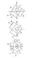
- the optical fiber scanner according to Patent Document 1 has a structure in which two piezoelectric elements are bonded to the outer surface of the elastic member to obtain two orthogonal vibrations, the problem as shown in FIG.
- the vibration direction is inclined because the structure is uniform.
- the shape of the scanning trajectory of the light by the optical fiber scanner is affected by the resonance frequency of the piezoelectric element for the X-axis direction and the piezoelectric element for the Y-axis direction.
- the number is a different value.
- the resonance frequency difference between the X-axis direction and the Y-axis direction becomes large, and it is difficult to obtain stable scanning performance.
- the present invention has been made in view of the above-described circumstances, and an optical fiber scanner capable of reducing the resonance frequency difference between the X-axis direction and the Y-axis direction of an optical fiber and obtaining stable scanning performance, and An object is to provide an illumination device and an observation device provided.
- an optical fiber having a longitudinal axis and emitting light from a distal end portion, a vibrating portion that vibrates the distal end portion of the optical fiber in a direction intersecting the longitudinal axis, and the optical fiber.
- a fixing portion that fixes the base end side of the piezoelectric element, wherein the vibration portion holds the optical fiber at a position closer to the base end side than the distal end portion, and a piezoelectric element that generates vibration when voltage is applied.
- An elastic member that transmits vibration of the element to the optical fiber, and the piezoelectric element is disposed along the longitudinal axis of the optical fiber and orthogonal to each other, and is sandwiched in the plate thickness direction by two electrodes It is arranged so as to fill a space between the strip-shaped first piezoelectric active region and the second piezoelectric active region and the adjacent end surfaces in the width direction of the first piezoelectric active region and the second piezoelectric active region.
- Piezoelectric inactivation connecting both piezoelectric active regions A cross section in a biaxial direction perpendicular to the longitudinal axis and perpendicular to the longitudinal axis of the optical fiber having a cross-sectional shape constituted by the piezoelectric element, the optical fiber and the elastic member at the position of the vibration part
- This is an optical fiber scanner having substantially the same second moment.
- the first piezoelectric active region when a voltage is applied to the first piezoelectric active region, the first piezoelectric active region is deformed in the longitudinal direction of the optical fiber, so that the optical fiber has the first diameter.
- the tip of the optical fiber is displaced in the first radial direction.
- the second piezoelectric active region when a voltage is applied to the second piezoelectric active region, the second piezoelectric active region is deformed in the longitudinal direction of the optical fiber, whereby the optical fiber is bent and deformed in the second radial direction.
- the tip of is displaced in the second radial direction.
- the light emitted from the tip of the optical fiber is scanned in the second radial direction intersecting the first radial direction. Therefore, light can be scanned two-dimensionally by applying a voltage simultaneously to the first piezoelectric active region and the second piezoelectric active region.
- the resonance frequencies can be made substantially equal in the X-axis direction and the Y-axis direction.
- the resonance frequency difference between the X-axis direction and the Y-axis direction can be reduced. Therefore, unnecessary vibration can be prevented and vibration at the tip of the optical fiber can be stabilized.
- the cross-sectional shape is substantially square. By doing so, it is possible to easily process a cross-sectional shape in which the cross-sectional secondary moments in the biaxial directions perpendicular to the longitudinal axis of the optical fiber and perpendicular to each other are substantially the same.
- the piezoelectric element traverses by arranging one first piezoelectric active region and one second piezoelectric active region orthogonally via one piezoelectric inactive region.
- the surface may be formed in a substantially L shape
- the elastic member may be formed in a cylindrical shape having a through hole that penetrates the optical fiber in the longitudinal direction and formed in a substantially square cross section.
- the inner surface (the inner surface of the first active region and the inner surface of the second active region) of one piezoelectric element formed in a substantially L-shaped cross section has a substantially square cross section.
- the optical fiber scanner Assembling can be simplified. Further, since the optical fiber is formed in a state of being previously incorporated in the elastic member in the assembly process of the optical fiber scanner, the optical fiber can be stably held.
- the piezoelectric element traverses by arranging one first piezoelectric active region and one second piezoelectric active region orthogonally via one piezoelectric inactive region.
- the elastic member may be formed in a substantially L-shaped cross section that sandwiches the optical fiber with the piezoelectric element.
- the optical fiber is placed in the longitudinal direction in a space surrounded by the inner surface of the piezoelectric element formed in a substantially L-shaped cross section and the inner surface of an elastic member formed in a substantially L-shaped cross section. Can be inserted. Furthermore, the optical fiber can be more stably held by supporting the outer peripheral surface of the optical fiber at four points by the inner surface of the piezoelectric element and the inner surface of the elastic member. Furthermore, since the optical fiber is not inserted into a through hole provided in the elastic member, the assembly of the optical fiber scanner can be simplified.
- the piezoelectric element traverses by arranging one of the first piezoelectric active regions and two of the second piezoelectric active regions orthogonally via the two piezoelectric inactive regions.
- the elastic member may be formed in a cylindrical shape having a through-hole that penetrates the optical fiber in the longitudinal direction and having a substantially square cross section.
- the elastic member incorporating the optical fiber is disposed in the space of the piezoelectric element formed in a substantially U-shaped cross section, so that the elastic member is attached to the piezoelectric element formed in a substantially L-shaped cross section.
- the displacement of the elastic member can be prevented, and the assembly accuracy can be improved.
- the piezoelectric element traverses by arranging one of the first piezoelectric active regions and two of the second piezoelectric active regions orthogonally via the two piezoelectric inactive regions.
- the elastic member may be formed in a substantially rectangular cross section that sandwiches the optical fiber with the piezoelectric element.
- the thickness dimension of the first piezoelectric active region may be formed larger than the thickness dimension of the second piezoelectric active region.
- a second aspect of the present invention includes a light source, the optical fiber scanner according to any one of the above that scans the light from the light source, and a condensing lens that collects the light scanned by the optical fiber scanner. It is a lighting device.
- an observation apparatus comprising: the above-described illumination device; and a light detection unit that detects return light from the subject when the subject is irradiated with light by the illumination device. is there.
- the resonance frequency difference between the X-axis direction and the Y-axis direction of the optical fiber can be reduced and stable vibration can be obtained at the same resonance frequency.
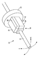
- FIG. 1 is an overall configuration diagram of an observation apparatus according to a first embodiment of the present invention. It is a longitudinal cross-sectional view along the longitudinal axis which shows the internal structure of the insertion part front-end
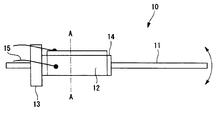
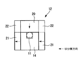
- FIG. 4B is a transverse cross-sectional view of the optical fiber scanner of FIG. 4A cut along line AA.
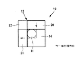
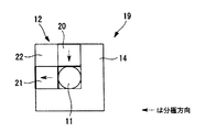
- FIG. 4B is a transverse sectional view showing a state where the optical fiber scanner of FIG. 4A is used.
- FIG. 6B is a cross-sectional view illustrating a first modification of the vibrating section in FIG. 6A.
- FIG. 6B is a cross-sectional view illustrating a second modification of the vibration unit in FIG. 6A.
- FIG. 6B is a cross-sectional view illustrating a third modification of the vibrating section in FIG. 6A.
- the observation apparatus 1 includes an endoscope 30 having an elongated insertion portion 30a, a control device main body 40 connected to the endoscope 30, and the control device main body 40. And a display 50 connected thereto.
- the observation apparatus 1 scans illumination light emitted from the distal end of the insertion portion 30a of the endoscope 30 along a spiral scanning locus B on the subject A, and acquires an image of the subject A. It is a mirror device.
- the observation apparatus 1 detects an illumination device 2 that irradiates the subject A with illumination light, and return light that returns from the subject A when the illumination light is irradiated.
- a light detection unit 3 such as a photodiode, and a control unit 4 that drives and controls the illumination device 2 and the light detection unit 3 are provided.
- the photodetector 3 and the drive unit 4 are provided in the control device main body 40.
- the illuminating device 2 includes a light source 5 that generates light such as illumination light, an optical fiber scanner 10 that scans light from the light source 5, and a front end side of the optical fiber scanner 10.
- a condensing lens 6 that condenses the emitted illumination light
- an elongated cylindrical frame 7 that houses the optical fiber scanner 10 and the condensing lens 6, and a circumferential arrangement on the outer peripheral surface of the frame 7.
- a detection optical fiber 8 that guides return light (for example, reflected light or fluorescent light of illumination light) from the subject A to the light detection unit 3.
- the optical fiber scanner 10 includes an illumination optical fiber (optical fiber) 11 such as a multimode fiber or a single mode fiber that guides light from the light source 5 and emits it from the tip.
- An elastic member 14 fixed to the outer peripheral surface of the illumination optical fiber 11 and holding the optical fiber 11; a piezoelectric element 12 fixed to the outer surface of the elastic member 14; and a base end side of the elastic member 14.
- a fixing portion 13 for fixing the illumination optical fiber 11 to the frame body 7.
- a lead wire 15 for supplying an alternating voltage is connected to the piezoelectric element 12.
- the light source 5 is connected to the proximal end of the illumination optical fiber 11.
- the illumination optical fiber 11 is a multimode fiber or a single mode fiber made of an elongated glass material having a circular cross section, and is arranged along the longitudinal direction of the frame body 7.
- the distal end of the illumination optical fiber 11 is disposed in the vicinity of the distal end portion inside the frame body 7, and the proximal end of the illumination optical fiber 11 extends from the proximal end of the frame body 7 to the outside and is connected to the light source 5. ing.
- the piezoelectric element 12 is made of a uniform piezoelectric ceramic material such as lead zirconate titanate (PZT), and has a seamless integrated structure. As shown in FIGS. 3 to 4C, the piezoelectric element 12 has a substantially L-shaped cross section in the XY plane orthogonal to the longitudinal direction. Such a piezoelectric element 12 is produced, for example, by cutting out from a prismatic piezoelectric material.
- the longitudinal direction of the illumination optical fiber 11 will be referred to as a Z-axis direction, and two radial directions of the illumination optical fiber 11 that are orthogonal to each other will be described as an X-axis direction and a Y-axis direction.
- the piezoelectric element 12 includes a first piezoelectric active region 20 adjacent to the X-axis direction along the longitudinal axis of the illumination optical fiber 11, and the longitudinal axis of the illumination optical fiber 11.
- the second piezoelectric active region 21 adjacent in the Y-axis direction, and the space between the adjacent end surfaces in the width direction of the first piezoelectric active region 20 and the second piezoelectric active region 21 are arranged to fill
- the piezoelectric inactive region 22 connects the two piezoelectric active regions.
- the outer surfaces of the first piezoelectric active region 20 and the second piezoelectric active region 21 of the piezoelectric element 12 are subjected to + (plus) electrode treatment, and the inner surface is subjected to ⁇ (minus) electrode treatment. As a result, it is polarized in the plate thickness direction from the + pole to the-pole, and when a voltage is applied, it expands and contracts (lateral effect) in a direction perpendicular to the polarization direction.
- Electrodes 23 are formed on the inner surface and the outer surface of the first piezoelectric active region 20, and the piezoelectric material is polarized in the X-axis direction in the region between the inner surface and the outer surface.
- Electrodes 23 are also formed on the inner and outer surfaces of the second piezoelectric active region 21, and the piezoelectric material is polarized in the Y-axis direction in the region between the inner and outer surfaces.
- the arrow in FIG. 4B has shown the polarization direction.
- a voltage is applied to the piezoelectric element 12 from a lead wire 15 bonded to the outer surfaces of the first piezoelectric active region 20 and the second piezoelectric active region 21.
- an A-phase alternating voltage is applied to the first piezoelectric active region 20 and a B-phase alternating voltage is applied to the second piezoelectric active region 21 via the elastic member 14.
- the bending vibration is transmitted to the illumination optical fiber 11, and the exit end of the illumination optical fiber 11 is displaced in the X-axis direction and the Y-axis direction intersecting with the Z-axis direction to vibrate.
- the elastic member 14 is formed in a square cylinder shape, and as shown in FIG. 4B, the cross section viewed from the longitudinal direction (Z-axis direction) is formed in a substantially square shape. In the center of the elastic member 14, a through hole through which the illumination optical fiber 11 passes is formed.
- the elastic member 14 is formed of, for example, a conductive metal material or resin material such as zirconia (ceramic) or nickel.
- the flat inner surface of the first piezoelectric active region 20 and the flat inner surface of the second piezoelectric active region 21 of the piezoelectric element 12 are respectively fixed to the two flat outer surfaces of the elastic member 14 by an adhesive, whereby the vibrating unit 19 is used. Is forming. As shown in FIG. 4B, the cross section viewed from the longitudinal direction (Z-axis direction) constituted by the piezoelectric element 12, the optical fiber 11, and the elastic member 14 is formed in a substantially square shape at the position of the vibration unit 19. ing.
- the fixing portion 13 is a substantially annular conductive member having a central hole, and as shown in FIG. 3, the elastic member 14 located on the base end side of the piezoelectric element 12 is fitted in the central hole. It is fixed with an adhesive. As shown in FIG. 2, the outer peripheral surface of the fixing portion 13 is fixed to the inner wall of the frame body 7, the elastic member 14 is supported by the fixing portion 13 in a cantilever shape, and the distal end of the illumination optical fiber 11. The part is supported by the elastic member 14 in a cantilever shape having a free end at the tip. A GND line 16 is connected to the base end side of the elastic member 14.
- the fixing portion 13 is electrically connected to the inner surfaces of the first piezoelectric active region 20 and the second piezoelectric active region 21 of the piezoelectric element 12 via the elastic member 14, and the first piezoelectric activity of the piezoelectric element 12. It functions as a common GND when driving the region 20 and the second piezoelectric active region 21.
- the lead wire 15 and the GND wire 16 are made of conductive wire (for example, copper, aluminum, etc.). As shown in FIG. 2, the proximal end sides of the lead wire 15 and the GND wire 16 are connected to the control unit 4.
- the control unit 4 is operated, illumination light is supplied from the light source unit 5 to the illumination optical fiber 11, and piezoelectric is transmitted via the lead wire 15. An alternating voltage having a predetermined driving frequency is applied to the element 12.
- the first piezoelectric active region 20 to which the A-phase alternating voltage is applied expands and contracts in the Z-axis direction orthogonal to the polarization direction, so that the X-axis is provided at the tip of the illumination optical fiber 11 via the elastic member 14.
- Directional bending vibrations are transmitted.
- the illumination light emitted from the distal end of the optical fiber 11 for illumination is bent and oscillated in the X-axis direction at a frequency equal to the drive frequency of the alternating voltage, and oscillated in the X-axis direction.
- the second piezoelectric active region 21 to which the B-phase alternating voltage is applied expands and contracts in the Z-axis direction orthogonal to the polarization direction, thereby causing the tip of the illumination optical fiber 11 to pass through the elastic member 14.
- the bending vibration in the Y-axis direction is transmitted to.
- the illumination light emitted from the tip of the illumination optical fiber 11 is bent and vibrated in the Y-axis direction at a frequency equal to the drive frequency of the alternating voltage, and oscillated in the Y-axis direction.
- Return light from the subject A is received by the detection optical fiber 8, and its intensity is detected by the light detection unit 3.
- the control unit 4 causes the photodetector 3 to detect return light in synchronization with the scanning period of the illumination light, and generates an image of the subject A by associating the detected intensity of the return light with the scanning position of the illumination light.
- the generated image is output from the control device body 40 to the display 50 and displayed.
- the natural frequency in a general structure will be described.
- the natural frequency (resonance point) can be expressed by the following calculation formula (1).
- fn (kn 2 / 2 ⁇ ) ⁇ (EI / ⁇ AL 4 )
- fn natural frequency
- kn constant corresponding to eigenvalue
- E longitudinal elastic modulus
- I secondary moment of section
- A cross-sectional area
- L length
- ⁇ density
- the piezoelectric element 12 includes one first piezoelectric active region 20 and one second piezoelectric active region 21 as one piezoelectric inactive region.
- the cross section is formed so as to have a substantially L-shaped cross section. More specifically, by joining the outer surface of the elastic member 14 formed in a substantially square cross section to the inner surface of the first active region 20 and the inner surface of the second active region 21 of the piezoelectric element 12, It has an equivalent structure in which the cross-sectional shape at the position of the vibration part 19 is formed in a substantially square shape. Since it is formed in this way, even if the vibration direction is tilted due to non-uniformity such as specific gravity, as shown in FIG.
- the natural frequency becomes substantially the same value, and the resonance frequency difference between the X-axis direction and the Y-axis direction of the optical fiber becomes small, so that vibrations in the X-axis direction and the Y-axis direction can be stabilized.
- the cross section at the position of the vibration portion 19 is formed in a substantially square shape by combining the piezoelectric element 12 formed in a substantially L-shaped cross section and the elastic member 14 formed in a substantially square cross section, It is possible to easily process a cross-sectional shape in which the cross-sectional secondary moments in the X-axis direction and the Y-axis direction orthogonal to each other in the longitudinal direction (Z-axis direction) of the illumination optical fiber 11 are substantially the same.
- the elastic member 14 is positioned at a predetermined position with respect to the piezoelectric element 12 by abutting the outer surface of the elastic member 14 against two inner surfaces of the piezoelectric element 12 that are perpendicular to each other. Matching becomes unnecessary. Thereby, there is an advantage that the assembly accuracy of the optical fiber scanner 10 can be improved and the optical fiber scanner 1 having a desired scanning performance can be stably manufactured. Furthermore, since the wiring 15 for supplying power to the piezoelectric element 12 only needs to be installed at two places in total, the first piezoelectric active region 20 and the second piezoelectric active region 21, wiring work is reduced. The assembly of the optical fiber scanner 10 can be simplified.
- the optical fiber scanner 10, the illumination device 2, and the observation device 1 according to the second embodiment of the present invention will be described with reference to FIGS. 5A and 5B.
- the configuration different from the first embodiment will be mainly described, and the configuration common to the first embodiment will be denoted by the same reference numerals and the description thereof will be omitted.
- the elastic member 14 is formed in a polygonal column shape having a substantially L-shaped cross section viewed from the longitudinal direction (Z-axis direction). This is different from the first embodiment.
- the elastic member 14 has a seamless integrated structure. Such an elastic member 14 is produced by cutting out from a prismatic material, for example.
- the elastic member 14 is smaller than the piezoelectric element 12 and has a cross-section that is similar to the piezoelectric element 12, that is, substantially L-shaped. As shown in FIG. 5A, the two end surfaces of the elastic member 14 are joined to the two inner surfaces (the inner surface of the first active region 20 and the inner surface of the second active region 21) of the piezoelectric element 12, It has an equivalent structure in which the cross-sectional shape at the position of the vibration part 19 is formed in a substantially square shape. By doing in this way, the cross-sectional shape from which the cross-sectional secondary moment in a X-axis direction and a Y-axis direction becomes substantially the same can be processed easily. Further, since alignment other than the longitudinal direction is not required, the assembling property of the optical fiber scanner 10 can be improved.
- the piezoelectric element 12 has two inner surfaces which are the inner surface of the first piezoelectric active region 20 and the inner surface of the second piezoelectric active region 21, and the elastic member 14 has two inner surfaces which are substantially L-shaped inner surfaces. Have.
- the two inner surfaces of the piezoelectric element 12 and the two inner surfaces of the elastic member 14 have the same height dimension that is substantially the same as the radius of the illumination optical fiber 11.
- the illumination optical fiber 11 is disposed in a space surrounded by the inner surface of the first piezoelectric active region 20, the inner surface of the second piezoelectric active region 21, and the two inner surfaces of the elastic member 14, and the illumination optical fiber 11. Are supported at four points which are shifted by 90 ° in the circumferential direction by these four inner surfaces. Therefore, the illumination optical fiber 11 can be held more stably. Further, it is not necessary to provide the through hole for inserting the illumination optical fiber 11 in the elastic member 14, and the processing of the illumination optical fiber 11 becomes easy. Furthermore, since the illumination optical fiber 11 may be inserted into a space surrounded by the two inner surfaces of the piezoelectric member 12 and the two inner surfaces of the elastic member 14, the assembly of the optical fiber scanner 10 can be further simplified. it can.
- the elastic member 14 is smaller than the piezoelectric element 12 and has a similar shape to the piezoelectric element 12, but instead, the elastic member 14 is piezoelectric as shown in FIG. 5B. It may be larger than the element 12 and similar to the piezoelectric element 12. In this case, as shown in FIG. 5B, the two end faces of the piezoelectric element 12 are joined to the two inner side faces of the elastic member 14 so that the cross-sectional shape at the position of the vibrating portion 19 is formed in a substantially square shape. It becomes a structure.
- the optical fiber scanner 10 has a piezoelectric element 12 having a substantially U-shaped cross section in the XY plane perpendicular to the longitudinal direction. Different from the first and second embodiments.
- the piezoelectric inactive region 22 includes both end portions of one first piezoelectric active region 20 and end portions located on the first piezoelectric active region 20 side in the two second piezoelectric active regions 21. It is provided in between. Therefore, the piezoelectric element 12 is open on the opposite side of the first piezoelectric active region 20.
- the elastic member 14 is formed in a substantially square cross section as viewed from the longitudinal direction (Z-axis direction).
- a through hole is formed in the center of the elastic member 14 to allow the illumination optical fiber 11 to pass therethrough.
- the three outer surfaces of the elastic member 14 are bonded to the three inner surfaces (the inner surface of one first active region 20 and the inner surface of two second active regions 21) of the piezoelectric element 12.
- the cross-sectional shape at the position of the vibration part 19 is an equivalent structure formed in a substantially square shape.
- the cross-sectional shape from which the cross-sectional secondary moment in a X-axis direction and a Y-axis direction becomes substantially the same can be processed easily. Further, since alignment other than the longitudinal direction is not required, the assembling property of the optical fiber scanner 10 can be improved.
- the piezoelectric element 12 has three inner surfaces which are the inner surface of one first piezoelectric active region 20 and the inner surfaces of two second piezoelectric active regions 21, and as shown in FIG. Three outer surfaces are in contact with the three inner surfaces.
- the illumination optical fiber 11 is inserted in the Z-axis direction into a through hole provided in the center of the elastic member 14.
- the disposition of the elastic member 14 with respect to the piezoelectric element 12 is improved as compared with the first embodiment and the second embodiment. That is, when the vibrating portion 19 is formed by combining the piezoelectric element 12 having a substantially L-shaped cross section with the elastic member 14 having a substantially square or L-shaped cross section, the elastic member 14 is formed as shown in FIGS. 8A and 8B. In this embodiment, the elastic member 14 is disposed in the space of the piezoelectric element 12 formed in a substantially U-shaped cross section. Therefore, positional deviation in the X-axis direction can be prevented, and assembly accuracy can be improved.
- the elastic member 14 is formed to have a substantially square cross section, and the illumination optical fiber 11 is passed through the center thereof. Instead, the elastic member 14 has a substantially rectangular cross section.
- the optical fiber 11 for illumination is arranged in a space surrounded by the inner surface of the piezoelectric element 12 and the outer surface of the elastic member 14 with a shape (see FIGS. 6B and 6D) and a substantially U-shaped cross section (see FIG. 6C). It is good to do. By doing in this way, since the outer peripheral surface of the illumination optical fiber 11 is supported at four points shifted by 90 ° in the circumferential direction, the illumination optical fiber 11 can be held more stably.
- the through hole for inserting the illumination optical fiber 11 in the elastic member 14 it is not necessary to provide the through hole for inserting the illumination optical fiber 11 in the elastic member 14, and the processing of the illumination optical fiber 11 becomes easy. Furthermore, since the illumination optical fiber 11 may be inserted into a space surrounded by the inner surface of the piezoelectric element 12 and the outer surface of the elastic member 14, the assembly of the optical fiber scanner 10 can be further simplified.
- the thickness dimension of the first piezoelectric active region 20 of the piezoelectric element 12 may be formed larger than the thickness dimension of the second piezoelectric active region 21.
- the first piezoelectric active region 20 is formed to have a thickness dimension approximately twice that of the second piezoelectric active region 21.
- the first piezoelectric active region 20 is approximately twice as thick as the second piezoelectric active region 21, the X-axis direction and the Y-axis direction when the alternating voltages of the A phase and the B phase are equal.
- the amplitude of the bending vibration at the tip of the optical fiber 11 for light illumination becomes equal. That is, it is only necessary to supply an alternating voltage having the same magnitude to each of the first piezoelectric active region 20 and the second piezoelectric active region 21, and the control of the alternating voltage can be facilitated.
Landscapes
- Physics & Mathematics (AREA)
- Health & Medical Sciences (AREA)
- Life Sciences & Earth Sciences (AREA)
- Optics & Photonics (AREA)
- Surgery (AREA)
- General Physics & Mathematics (AREA)
- Biomedical Technology (AREA)
- General Health & Medical Sciences (AREA)
- Pathology (AREA)
- Engineering & Computer Science (AREA)
- Nuclear Medicine, Radiotherapy & Molecular Imaging (AREA)
- Heart & Thoracic Surgery (AREA)
- Medical Informatics (AREA)
- Molecular Biology (AREA)
- Animal Behavior & Ethology (AREA)
- Radiology & Medical Imaging (AREA)
- Public Health (AREA)
- Veterinary Medicine (AREA)
- Biophysics (AREA)
- Astronomy & Astrophysics (AREA)
- Instruments For Viewing The Inside Of Hollow Bodies (AREA)
- Endoscopes (AREA)
- Mechanical Optical Scanning Systems (AREA)
Abstract
光ファイバのX軸方向とY軸方向の共振周波数差を小さくし、同一の共振周波数で安定した走査性能を得る。本発明に係る光ファイバスキャナ(10)は、光ファイバ(11)と、光ファイバ(11)を振動させる振動部(19)と、光ファイバ(11)を固定する固定部(13)とを備える。振動部(19)は、圧電素子(12)と、圧電素子(12)の振動を光ファイバ(11)に伝達する弾性部材(14)とを備える。圧電素子(12)は、第1の圧電活性領域(20)および第2の圧電活性領域(21)と、これらの隣接する端面間を埋めるように配置された圧電不活性領域(22)とを備える。振動部(19)の位置において、圧電素子(12)、光ファイバ(11)および弾性部材(14)によって構成される横断面形状の光ファイバ(11)の長手軸に直交しかつ互いに直交する2軸方向の断面二次モーメントが略同一である。
Description
本発明は、光ファイバスキャナ、照明装置および観察装置に関するものである。
従来、X軸方向に振動する圧電素子とY軸方向に振動する圧電素子の合計2枚の圧電素子を備え、X軸方向に振動する圧電素子上に光ファイバが配置された光ファイバスキャナが知られている(例えば、特許文献1参照。)。この光ファイバスキャナでは、共振周波数で駆動される圧電素子がX軸方向に振動し、非共振周波数で駆動される圧電素子がY軸方向に振動することによって光ファイバを屈曲振動させて光ファイバの先端から射出される光を二次元的に走査するようになっている。
しかしながら、特許文献1に係る光ファイバスキャナでは、X軸方向に振動する圧電素子とY軸方向に振動する圧電素子の断面積や断面二次モーメントが異なるため、X軸方向と、Y軸方向とでは共振周波数が異なる。このため、X軸方向に振動する圧電素子とY軸方向に振動する圧電素子を同一の共振周波数で動かそうとする場合、X軸方向とY軸方向の間で共振周波数差が発生するため不要な振動が発生し、振動を安定させることが難しいという問題がある。
また、特許文献1に係る光ファイバスキャナを、弾性部材の外側面に2枚の圧電素子を接着して直交する2軸の振動を得られる構造にしたとしても、図7に示されるような不均等な構造となるため振動方向が傾く。光ファイバスキャナによる光の走査軌跡の形状は、X軸方向用の圧電素子とY軸方向用の圧電素子の共振周波数に影響されるが、傾いた方向に異なる断面二次モーメントとなると、固有振動数が異なる値となる。その結果、X軸方向とY軸方向との共振周波数差が大きくなり、安定した走査性能を得ることが難しいという問題がある。
本発明は、上述した事情に鑑みてなされたものであって、光ファイバのX軸方向とY軸方向の共振周波数差を小さくし、安定した走査性能を得ることができる光ファイバスキャナおよびこれを備える照明装置および観察装置を提供することを目的とする。
上記目的を達成するため、本発明は以下の手段を提供する。
本発明の第1の態様は、長手軸を有し、先端部から光を射出する光ファイバと、該光ファイバの先端部を前記長手軸に交差する方向に振動させる振動部と、前記光ファイバの基端側を固定する固定部とを備え、前記振動部が、電圧の印加によって振動を発生する圧電素子と、前記先端部よりも基端側の位置において前記光ファイバを保持し、前記圧電素子の振動を前記光ファイバに伝達する弾性部材とを備え、前記圧電素子が、前記光ファイバの長手軸に沿ってかつ互いに直交して配置され、2枚の電極によって板厚方向に挟まれた帯板状の第1の圧電活性領域および第2の圧電活性領域と、前記第1の圧電活性領域および前記第2の圧電活性領域の隣接する幅方向の端面間の空間を埋めるように配置され両圧電活性領域を接続する圧電不活性領域とを備え、前記振動部の位置において、前記圧電素子、前記光ファイバおよび前記弾性部材によって構成される横断面形状の前記光ファイバの前記長手軸に直交しかつ互いに直交する2軸方向の断面二次モーメントが略同一である光ファイバスキャナである。
本発明の第1の態様は、長手軸を有し、先端部から光を射出する光ファイバと、該光ファイバの先端部を前記長手軸に交差する方向に振動させる振動部と、前記光ファイバの基端側を固定する固定部とを備え、前記振動部が、電圧の印加によって振動を発生する圧電素子と、前記先端部よりも基端側の位置において前記光ファイバを保持し、前記圧電素子の振動を前記光ファイバに伝達する弾性部材とを備え、前記圧電素子が、前記光ファイバの長手軸に沿ってかつ互いに直交して配置され、2枚の電極によって板厚方向に挟まれた帯板状の第1の圧電活性領域および第2の圧電活性領域と、前記第1の圧電活性領域および前記第2の圧電活性領域の隣接する幅方向の端面間の空間を埋めるように配置され両圧電活性領域を接続する圧電不活性領域とを備え、前記振動部の位置において、前記圧電素子、前記光ファイバおよび前記弾性部材によって構成される横断面形状の前記光ファイバの前記長手軸に直交しかつ互いに直交する2軸方向の断面二次モーメントが略同一である光ファイバスキャナである。
本発明の第1の態様によれば、第1の圧電活性領域に電圧が印加されると、該第1の圧電活性領域が光ファイバの長手方向に変形することによって光ファイバが第1の径方向に屈曲変形し、光ファイバの先端が第1の径方向に変位する。これにより、光ファイバの先端から射出される光が第1の径方向に走査される。同様に、第2の圧電活性領域に電圧が印加されると、該第2の圧電活性領域が光ファイバの長手方向に変形することによって光ファイバが第2の径方向に屈曲変形し、光ファイバの先端が第2の径方向に変位する。これにより、光ファイバの先端から射出される光が、第1の径方向に交差する第2の径方向に走査される。したがって、第1の圧電活性領域および第2の圧電活性領域に同時に電圧を印加することによって、光を二次元的に走査することができる。
この場合に、振動部の位置において、圧電素子、光ファイバおよび弾性部材によって構成される横断面形状の光ファイバの長手軸に直交しかつ互いに直交する2軸方向の断面二次モーメントが略同一であるので、光ファイバスキャナの比重等が不均等になり振動方向が傾いたとしても、X軸方向と、Y軸方向とで共振周波数を略等しくすることができる。これにより、X軸方向に振動する圧電素子とY軸方向に振動する圧電素子を同一の共振周波数で動かそうとする場合、X軸方向とY軸方向の間で共振周波数差を小さくすることができるので、不要な振動を防止して光ファイバ先端部の振動を安定させることできる。
上記第1の態様においては、前記横断面形状を略正方形にすることが好ましい。
このようにすることで、光ファイバの長手軸に直交しかつ互いに直交する2軸方向の断面二次モーメントが略同一となる横断面形状を、容易に加工することができる。
このようにすることで、光ファイバの長手軸に直交しかつ互いに直交する2軸方向の断面二次モーメントが略同一となる横断面形状を、容易に加工することができる。
上記第1の態様においては、前記圧電素子が、1つの前記第1の圧電活性領域と1つの前記第2の圧電活性領域とを1つの前記圧電不活性領域を介して直交配置することで横断面略L字形に形成され、前記弾性部材が、前記光ファイバを長手方向に貫通させる貫通孔を有し横断面略正方形に形成された筒状に形成されることとしてもよい。
このようにすることで、横断面略L字形に形成された1枚の圧電素子の内側面(第1の活性領域の内側面と第2の活性領域の内側面)に、横断面略正方形に形成された筒状の弾性部材の外側面を接合するだけで、振動部の位置における圧電素子、光ファイバおよび弾性部材によって構成される横断面形状を容易に略正方形状に形成することができる。また、長手方向以外の位置合わせが不要となるので、光ファイバスキャナの組立性を向上させることができる。さらに、圧電素子に電力を供給するための配線を、第1の圧電活性領域と1つの第2の圧電活性領域の合計2箇所に設置するだけでよいので、配線作業が少なくなり、光ファイバスキャナの組立を簡略化することができる。
また、光ファイバスキャナの組立工程において、あらかじめ光ファイバを弾性部材に組み込んだ状態に形成されるので、光ファイバを安定的に保持することができる。
また、光ファイバスキャナの組立工程において、あらかじめ光ファイバを弾性部材に組み込んだ状態に形成されるので、光ファイバを安定的に保持することができる。
上記第1の態様においては、前記圧電素子が、1つの前記第1の圧電活性領域と1つの前記第2の圧電活性領域とを1つの前記圧電不活性領域を介して直交配置することで横断面略L字形に形成され、前記弾性部材が、前記光ファイバを前記圧電素子との間に挟む横断面略L字形に形成されることとしてもよい。
このようにすることで、横断面略L字形に形成された圧電素子の端部と、横断面略L字形に形成された弾性部材の端部とが互いに接するように天地逆に組み合わせるだけで、振動部の位置における圧電素子、光ファイバおよび弾性部材によって構成される横断面形状を容易に略正方形状に形成することができる。このため、長手方向以外の位置合わせが不要となるので、光ファイバスキャナの組立性を向上させることができる。
また、光ファイバスキャナの組立工程において、横断面略L字形に形成された圧電素子の内面と、横断面略L字形に形成された弾性部材の内面によって囲まれる空間内に光ファイバを長手方向に挿入することができる。さらに、圧電素子の内面と、弾性部材の内面とによって光ファイバの外周面を4点支持することで、光ファイバをより安定的に保持することができる。さらに、光ファイバを弾性部材に設けた貫通孔に挿入作業が不要となるため、光ファイバスキャナの組立を簡略化することができる。
また、光ファイバスキャナの組立工程において、横断面略L字形に形成された圧電素子の内面と、横断面略L字形に形成された弾性部材の内面によって囲まれる空間内に光ファイバを長手方向に挿入することができる。さらに、圧電素子の内面と、弾性部材の内面とによって光ファイバの外周面を4点支持することで、光ファイバをより安定的に保持することができる。さらに、光ファイバを弾性部材に設けた貫通孔に挿入作業が不要となるため、光ファイバスキャナの組立を簡略化することができる。
上記第1の態様においては、前記圧電素子が、1つの前記第1の圧電活性領域と2つの前記第2の圧電活性領域とを2つの前記圧電不活性領域を介して直交配置することで横断面略U字形に形成され、前記弾性部材が、前記光ファイバを長手方向に貫通させる貫通孔を有し横断面略正方形に形成された筒状に形成されることとしてもよい。
このようにすることで、光ファイバを組み込んだ弾性部材が、横断面略U字形に形成された圧電素子の空間に配置されるので、横断面略L字形に形成された圧電素子に弾性部材を組み合わせる場合に比べ、弾性部材の位置ずれを防ぐことができ、組立精度を向上させることができる。
このようにすることで、光ファイバを組み込んだ弾性部材が、横断面略U字形に形成された圧電素子の空間に配置されるので、横断面略L字形に形成された圧電素子に弾性部材を組み合わせる場合に比べ、弾性部材の位置ずれを防ぐことができ、組立精度を向上させることができる。
上記第1の態様においては、前記圧電素子が、1つの前記第1の圧電活性領域と2つの前記第2の圧電活性領域とを2つの前記圧電不活性領域を介して直交配置することで横断面略U字形に形成され、前記弾性部材が、前記光ファイバを前記圧電素子との間に挟む横断面略長方形に形成されることとしてもよい。
このようにすることで、光ファイバおよび弾性部材が、横断面略U字形に形成された圧電素子の空間に配置されるので、横断面略L字形に形成された圧電素子に弾性部材を組み合わせる場合に比べ、光ファイバや弾性部材の位置ずれを防ぐことができ、組立精度を向上させることができる。
このようにすることで、光ファイバおよび弾性部材が、横断面略U字形に形成された圧電素子の空間に配置されるので、横断面略L字形に形成された圧電素子に弾性部材を組み合わせる場合に比べ、光ファイバや弾性部材の位置ずれを防ぐことができ、組立精度を向上させることができる。
上記第1の態様においては、前記第1の圧電活性領域の厚さ寸法が、前記第2の圧電活性領域の厚さ寸法よりも大きく形成されていることとしてもよい。
このようにすることで、X軸方向における光ファイバの屈曲振動の共振周波数とY軸方向における光ファイバの屈曲振動の共振周波数とを近しくし、光ファイバの屈曲振動をより安定させることができる。
このようにすることで、X軸方向における光ファイバの屈曲振動の共振周波数とY軸方向における光ファイバの屈曲振動の共振周波数とを近しくし、光ファイバの屈曲振動をより安定させることができる。
本発明の第2の態様は、光源と、該光源からの光を走査する上記いずれかに記載の光ファイバスキャナと、該光ファイバスキャナにより走査された光を集光する集光レンズとを備える照明装置である。
また、本発明の第3の態様は、上記記載の照明装置と、該照明装置により被写体に光が照射されたときに、該被写体からの戻り光を検出する光検出部とを備える観察装置である。
また、本発明の第3の態様は、上記記載の照明装置と、該照明装置により被写体に光が照射されたときに、該被写体からの戻り光を検出する光検出部とを備える観察装置である。
本発明によれば、光ファイバのX軸方向とY軸方向の共振周波数差を小さくし、同一の共振周波数で安定した振動を得ることができるという効果を奏する。
(第1の実施形態)
以下に、本発明の第1の実施形態に係る光ファイバスキャナ10、照明装置2および観察装置1について図1から図4Cを参照して説明する。
本実施形態に係る観察装置1は、図1に示されるように、細長い挿入部30aを有する内視鏡30と、該内視鏡30に接続された制御装置本体40と、該制御装置本体40に接続されたディスプレイ50とを備えている。観察装置1は、内視鏡30の挿入部30aの先端から射出される照明光を被写体A上でスパイラル状の走査軌跡Bに沿って走査し、被写体Aの画像を取得する光走査型内視鏡装置である。
以下に、本発明の第1の実施形態に係る光ファイバスキャナ10、照明装置2および観察装置1について図1から図4Cを参照して説明する。
本実施形態に係る観察装置1は、図1に示されるように、細長い挿入部30aを有する内視鏡30と、該内視鏡30に接続された制御装置本体40と、該制御装置本体40に接続されたディスプレイ50とを備えている。観察装置1は、内視鏡30の挿入部30aの先端から射出される照明光を被写体A上でスパイラル状の走査軌跡Bに沿って走査し、被写体Aの画像を取得する光走査型内視鏡装置である。
本実施形態に係る観察装置1は、図1および2に示されるように、被写体Aに照明光を照射する照明装置2と、照明光が照射されることによって被写体Aから戻る戻り光を検出するフォトダイオードのような光検出部3と、照明装置2および光検出部3を駆動制御する制御部4とを備えている。光検出器3および駆動部4は制御装置本体40内に設けられている。
照明装置2は、照明光などの光を発生する光源5と、該光源5からの光を走査する光ファイバスキャナ10と、該光ファイバスキャナ10よりも先端側に配置され、光ファイバスキャナ10から射出された照明光を集光させる集光レンズ6と、光ファイバスキャナ10および集光レンズ6を収納する細長い筒状の枠体7と、該枠体7の外周面上に周方向に配列して設けられ、被写体Aからの戻り光(例えば、照明光の反射光や蛍光)を光検出部3に導光する検出用光ファイバ8とを備えている。
光ファイバスキャナ10は、図1から図4Aに示されるように、光源5からの光を導光し先端から射出させるマルチモードファイバまたはシングルモードファイバのような照明用光ファイバ(光ファイバ)11と、該照明用光ファイバ11の外周面に固定されてこの光ファイバ11を保持する弾性部材14と、該弾性部材14の外面に固定された圧電素子12と、弾性部材14の基端側に設けられ、照明用光ファイバ11を枠体7に固定する固定部13とを備えている。圧電素子12には、交番電圧を供給するためのリード線15が接続されている。光源5は照明用光ファイバ11の基端に接続されている。
照明用光ファイバ11は、横断面円形の細長いガラス材からなるマルチモードファイバまたはシングルモードファイバであり、枠体7の長手方向に沿って配されている。照明用光ファイバ11の先端は、枠体7の内部の先端部近傍に配されており、照明用光ファイバ11の基端は、枠体7の基端から外部へ延びて光源5に接続されている。
圧電素子12は、例えば、チタン酸ジルコン酸鉛(PZT)などの全体にわたって均質な圧電セラミックス材料からなり、継ぎ目の無い一体構造を有する。圧電素子12は、図3から図4Cに示されるように長手方向と直交するXY平面における横断面が略L字形に形成されている。このような圧電素子12は、例えば、角柱状の圧電材料から切り出すことによって作製される。
以下、照明用光ファイバ11の長手方向をZ軸方向とし、照明用光ファイバ11の互いに直交する2つの径方向をX軸方向およびY軸方向として説明する。
以下、照明用光ファイバ11の長手方向をZ軸方向とし、照明用光ファイバ11の互いに直交する2つの径方向をX軸方向およびY軸方向として説明する。
圧電素子12は、図3および図4Bに示されるように、照明用光ファイバ11の長手軸に沿い、X軸方向に隣接する第1の圧電活性領域20と、照明用光ファイバ11の長手軸に沿い、Y軸方向に隣接する第2の圧電活性領域21と、第1の圧電活性領域20と第2の圧電活性領域21の隣接する幅方向の端面間の空間を埋めるように配置された両圧電活性領域を接続する圧電不活性領域22とから構成されている。
圧電素子12の第1の圧電活性領域20および第2の圧電活性領域21の外面には+(プラス)の電極処理が施され、内面には-(マイナス)の電極処理が施されている。これによって+極から-極に向かって板厚方向に分極しており、電圧を印加した時に分極方向に対して直行する方向に伸縮振動(横効果)する。
第1の圧電活性領域20の内面および外面には電極23が形成されており、内面と外面との間の領域において圧電材料がX軸方向に分極している。また、第2の圧電活性領域21の内面および外面にも電極23が形成されており、内面と外面との間の領域において圧電材料がY軸方向に分極している。なお、図4B中の矢印は分極方向を示している。
第1の圧電活性領域20の内面および外面には電極23が形成されており、内面と外面との間の領域において圧電材料がX軸方向に分極している。また、第2の圧電活性領域21の内面および外面にも電極23が形成されており、内面と外面との間の領域において圧電材料がY軸方向に分極している。なお、図4B中の矢印は分極方向を示している。
圧電素子12には、第1の圧電活性領域20および第2の圧電活性領域21の外面に接着されるリード線15から電圧が印加されるようになっている。具体的には、第1の圧電活性領域20にはA相の交番電圧が印加され、第2の圧電活性領域21にはB相の交番電圧が印加されることで、弾性部材14を介して屈曲振動が照明用光ファイバ11に伝達され、照明用光ファイバ11の射出端が、Z軸方向に交差するX軸方向およびY軸方向に変位させられて振動するようになっている。
弾性部材14は、四角筒状に形成されており、図4Bに示されるように、長手方向(Z軸方向)から見た横断面が略正方形状に形成されている。この弾性部材14の中央には、照明用光ファイバ11を貫通させる貫通孔が形成されている。弾性部材14は、例えば、ジルコニア(セラミック)やニッケル等の導電性を有する金属材料や樹脂材料から形成される。
圧電素子12の第1の圧電活性領域20の平坦な内面および第2の圧電活性領域21の平坦な内面が弾性部材14の2つの平坦な外面にそれぞれ接着剤により固定されることで振動部19を形成している。図4Bに示されるように、振動部19の位置において、圧電素子12、光ファイバ11および弾性部材14によって構成される長手方向(Z軸方向)から見た横断面は、略正方形状に形成されている。
固定部13は、中央孔を有する略円環状の導電性部材であり、図3に示されるように、圧電素子12よりも基端側に位置する弾性部材14を中央孔に嵌合させた状態で接着剤により固定されている。図2に示されるように、固定部13の外周面は、枠体7の内壁に固定されており、弾性部材14は片持ち梁状に固定部13によって支持され、照明用光ファイバ11の先端部は、先端を自由端とする片持ち梁状に弾性部材14によって支持されている。弾性部材14の基端側にはGND線16が接続されている。
固定部13は、弾性部材14を介して圧電素子12の第1の圧電活性領域20および第2の圧電活性領域21の内面と電気的に接続されており、圧電素子12の第1の圧電活性領域20および第2の圧電活性領域21を駆動する際の共通GNDとして機能するようになっている。
リード線15およびGND線16は、導電性を有する線材(例えば、銅、アルミニウム等)から形成されている。図2に示されるように、リード線15およびGND線16の基端側は制御部4に接続されている。
このように構成された本実施形態に係る光ファイバスキャナ10、照明装置2および観察装置1の作用について以下に説明する。
本実施形態に係る観察装置1を用いて被写体Aを観察するには、制御部4を作動させ、光源部5から照明用光ファイバ11に照明光を供給させるとともに、リード線15を介して圧電素子12に所定の駆動周波数を有する交番電圧を印加させる。
本実施形態に係る観察装置1を用いて被写体Aを観察するには、制御部4を作動させ、光源部5から照明用光ファイバ11に照明光を供給させるとともに、リード線15を介して圧電素子12に所定の駆動周波数を有する交番電圧を印加させる。
A相の交番電圧が印加された第1の圧電活性領域20は、分極方向に直交するZ軸方向に伸縮振動することにより、弾性部材14を介して、照明用光ファイバ11の先端にX軸方向の屈曲振動が伝達される。これにより、図3に示されるように、照明用光ファイバ11の先端が交番電圧の駆動周波数と等しい周波数でX軸方向に屈曲振動してX軸方向に振動し、先端から射出される照明光がX軸方向に直線的に走査される。
同様に、B相の交番電圧が印加された第2の圧電活性領域21は、分極方向に直交するZ軸方向に伸縮振動することにより、弾性部材14を介して、照明用光ファイバ11の先端にY軸方向の屈曲振動が伝達される。これにより、図3に示されるように、照明用光ファイバ11の先端が交番電圧の駆動周波数と等しい周波数でY軸方向に屈曲振動してY軸方向に振動し、先端から射出される照明光がY軸方向に直線的に走査される。
被写体Aからの戻り光は、検出用光ファイバ8によって受光され、その強度が光検出部3によって検出される。制御部4は、照明光の走査周期と同期して光検出器3に戻り光を検出させ、検出された戻り光の強度を照明光の走査位置と対応付けることによって被写体Aの画像を生成する。生成された画像は、制御装置本体40からディスプレイ50に出力されて表示される。
ここで、構造体一般における固有振動数ついて説明すると、固有振動数(共振点)は、下記の計算式(1)で表現することができる。
fn=(kn2/2π)√(EI/ρAL4)・・・・・(1)
fn:固有振動数
kn:固有値に対応した定数
E:縦弾性係数
I:断面二次モーメント
A:断面積
L:長さ
ρ:密度
従って、構造物一般において、式(1)に含まれる各パラメータを変更することにより、固有振動数を変化させることができる。
fn=(kn2/2π)√(EI/ρAL4)・・・・・(1)
fn:固有振動数
kn:固有値に対応した定数
E:縦弾性係数
I:断面二次モーメント
A:断面積
L:長さ
ρ:密度
従って、構造物一般において、式(1)に含まれる各パラメータを変更することにより、固有振動数を変化させることができる。
本実施形態に係る光ファイバスキャナ10は、図4Bに示されるように、圧電素子12が1つの第1の圧電活性領域20と1つの第2の圧電活性領域21とを1つの圧電不活性領域22を介して直交配置して横断面略L字形に形成されている。より詳細には、圧電素子12の第1の活性領域20の内側面と第2の活性領域21の内側面に、横断面略正方形に形成された弾性部材14の外側面を接合することで、振動部19の位置における横断面形状を略正方形状に形成した均等構造となっている。このように形成されているので、比重等の不均等さによって振動方向が傾いたとしても、図4Cに示されるように、傾いた方向に断面中心を中心として同一断面二次モーメントとなる。この結果、固有振動数が略同じ値となり、光ファイバのX軸方向とY軸方向との共振周波数差が小さくなるのでX軸方向とY軸方向の振動を安定させることができる。
また、振動部19の位置における横断面が、横断面略L字形に形成された圧電素子12と横断面略正方形に形成された弾性部材14とを組み合わせて略正方形状に形成されているので、照明用光ファイバ11の長手方向(Z軸方向)に互いに直交するX軸方向とY軸方向での断面二次モーメントとが略同一となる横断面形状を容易に加工することができる。
さらに、圧電素子12が有する互いに垂直な2つの内面に弾性部材14の外面を突き当てることによって、圧電素子12に対して弾性部材14が所定の位置に位置決めされることから、長手方向以外の位置合わせが不要となる。これにより、光ファイバスキャナ10の組立精度を向上し、所望の走査性能を有する光ファイバスキャナ1を安定的に製造することができるという利点がある。さらにまた、圧電素子12に電力を供給するための配線15を、第1の圧電活性領域20と第2の圧電活性領域21の合計2箇所に設置するだけでよいので、配線作業が少なくなり、光ファイバスキャナ10の組立を簡略化することができる。
(第2の実施形態)
次に、本発明の第2の実施形態に係る光ファイバスキャナ10、照明装置2および観察装置1について図5Aおよび図5Bを参照して説明する。本実施形態においては、第1の実施形態と異なる構成について主に説明し、第1の実施形態と共通する構成については同一の符号を付して説明を省略する。
次に、本発明の第2の実施形態に係る光ファイバスキャナ10、照明装置2および観察装置1について図5Aおよび図5Bを参照して説明する。本実施形態においては、第1の実施形態と異なる構成について主に説明し、第1の実施形態と共通する構成については同一の符号を付して説明を省略する。
本実施形態に係る光ファイバスキャナ10は、図5Aに示されるように、弾性部材14が長手方向(Z軸方向)から見た横断面が略L字形である多角柱状に形成されている点で、第1の実施形態と異なっている。弾性部材14は、継ぎ目の無い一体構造を有する。このような弾性部材14は、例えば、角柱状の材料から切り出すことによって作製される。
本実施形態においては、弾性部材14が圧電素子12よりも小さくかつ圧電素子12と相似形、即ち略L字形の横断面となっている。図5Aに示されるように、弾性部材14の2つの端面が圧電素子12の2つの内面(第1の活性領域20の内側面と第2の活性領域21の内側面)に接合することで、振動部19の位置における横断面形状を略正方形状に形成した均等構造となっている。
このようにすることで、X軸方向とY軸方向での断面二次モーメントが略同一となる横断面形状を容易に加工にすることができる。また、長手方向以外の位置合わせが不要となるので、光ファイバスキャナ10の組立性を向上させることができる。
このようにすることで、X軸方向とY軸方向での断面二次モーメントが略同一となる横断面形状を容易に加工にすることができる。また、長手方向以外の位置合わせが不要となるので、光ファイバスキャナ10の組立性を向上させることができる。
圧電素子12は第1の圧電活性領域20の内面と第2の圧電活性領域21の内面である2つの内面を有しており、弾性部材14は、略L字形の内面である2つの内面を有している。圧電素子12の2つの内面と、弾性部材14の2つの内面はそれぞれ、照明用光ファイバ11の半径と略同一である同一の高さ寸法を有している。
照明用光ファイバ11は、第1の圧電活性領域20の内面および第2の圧電活性領域21の内面と、弾性部材14の2つの内面によって囲まれた空間内に配置され、照明用光ファイバ11の外周面が、これら4つの内面によって周方向に90°ずつずれた4点において支持されている。したがって、照明用光ファイバ11をより安定的に保持することができる。また、弾性部材14には、照明用光ファイバ11を挿入するための貫通孔を設ける必要が無く、照明用光ファイバ11の加工が容易となる。さらに、圧電部材12の2つの内面と弾性部材14の2つの内面とによって囲まれた空間内に照明用光ファイバ11を挿入すればよいので、光ファイバスキャナ10の組立をより簡便化することができる。
なお、本実施形態においては、弾性部材14が圧電素子12よりも小さくかつ圧電素子12と相似形であることとしたが、これに代えて、図5Bに示されるように、弾性部材14が圧電素子12よりも大きくかつ圧電素子12と相似形であることとしてもよい。この場合には、図5Bに示されるように、弾性部材14の2つの内側面に圧電素子12の2つの端面を接合させて振動部19の位置における横断面形状を略正方形状に形成した均等構造となる。
このようにすることで、X軸方向とY軸方向での断面二次モーメントが略同一となる横断面形状を容易に加工にすることができる。なお、弾性部材14の材料として樹脂材料を用いることとすれば、振動部19全体のQ値が下がり、振動をさらに安定させることができる。
(第3の実施形態)
次に、本発明の第3の実施形態に係る光ファイバスキャナ10、照明装置2および観察装置1について図6Aから図6Dを参照して説明する。本実施形態においては、第1および第2の実施形態と異なる構成について主に説明し、第1および第2の実施形態と共通する構成については同一の符号を付して説明を省略する。
次に、本発明の第3の実施形態に係る光ファイバスキャナ10、照明装置2および観察装置1について図6Aから図6Dを参照して説明する。本実施形態においては、第1および第2の実施形態と異なる構成について主に説明し、第1および第2の実施形態と共通する構成については同一の符号を付して説明を省略する。
本実施形態に係る光ファイバスキャナ10は、図6Aから図6Dに示されるように、圧電素子12が、長手方向と直交するXY平面における横断面が略U字形に形成されている点で、第1および第2の実施形態と異なっている。
本実施形態において、圧電不活性領域22は、1つの第1圧電活性領域20の両端部と、2つの第2の圧電活性領域21における第1の圧電活性領域20側に位置する端部との間に設けられている。したがって、圧電素子12は、第1圧電活性領域20の反対側が開放されている。
本実施形態においては、弾性部材14が、長手方向(Z軸方向)から見た横断面が略正方形状に形成されている。そして、弾性部材14の中央には、照明用光ファイバ11を貫通させる貫通孔が形成されている。図6Aに示されるように、弾性部材14の3つの外面が圧電素子12の3つの内面(1つの第1の活性領域20の内側面と2つの第2の活性領域21の内側面)に接合することで、振動部19の位置における横断面形状を略正方形状に形成した均等構造となっている。
このようにすることで、X軸方向とY軸方向での断面二次モーメントが略同一となる横断面形状を容易に加工にすることができる。また、長手方向以外の位置合わせが不要となるので、光ファイバスキャナ10の組立性を向上させることができる。
このようにすることで、X軸方向とY軸方向での断面二次モーメントが略同一となる横断面形状を容易に加工にすることができる。また、長手方向以外の位置合わせが不要となるので、光ファイバスキャナ10の組立性を向上させることができる。
圧電素子12は1つの第1の圧電活性領域20の内面と2つの第2の圧電活性領域21の内面である3つの内面を有しており、図6Aに示されるように、弾性部材14の3つの外面がこの3つの内面に接している。照明用光ファイバ11は、弾性部材14の中央設けられた貫通孔にZ軸方向に挿入されている。
本実施形態においては、第1の実施形態および第2の実施形態と比較して、弾性部材14の圧電素子12に対する配置性が向上する。すなわち、横断面略L字形の圧電素子12に横断面略正方形や横断面略L字形の弾性部材14を組み合わせて振動部19を形成すると、図8Aや図8Bに示されるように、弾性部材14がX軸方向やY軸方向に位置ずれし、組立精度が低下する場合があるが、本実施形態では、弾性部材14が、横断面略U字形に形成された圧電素子12の空間内に配置されるので、X軸方向の位置ずれを防ぐことができ、組立精度を向上させることができる。
なお、本実施形態においては、弾性部材14を横断面略正方形状に形成し、その中央に照明用光ファイバ11を貫通させることとしたが、これに代えて、弾性部材14を横断面略矩形状(図6B、図6D参照)や、横断面略U字形(図6C参照)に形成し、圧電素子12の内面と弾性部材14の外面により囲まれた空間内に照明用光ファイバ11を配置することとしてもよい。
このようにすることで、照明用光ファイバ11の外周面が、周方向に90°ずつずれた4点において支持されるため、照明用光ファイバ11をより安定的に保持することができる。また、弾性部材14には、照明用光ファイバ11を挿入するための貫通孔を設ける必要が無く、照明用光ファイバ11の加工が容易となる。さらに、圧電素子12の内面と弾性部材14の外面により囲まれた空間内に照明用光ファイバ11を挿入すればよいので、光ファイバスキャナ10の組立をより簡便化することができる。
このようにすることで、照明用光ファイバ11の外周面が、周方向に90°ずつずれた4点において支持されるため、照明用光ファイバ11をより安定的に保持することができる。また、弾性部材14には、照明用光ファイバ11を挿入するための貫通孔を設ける必要が無く、照明用光ファイバ11の加工が容易となる。さらに、圧電素子12の内面と弾性部材14の外面により囲まれた空間内に照明用光ファイバ11を挿入すればよいので、光ファイバスキャナ10の組立をより簡便化することができる。
また、図6Aおよび図6Cに示されるように、圧電素子12の第1の圧電活性領域20の厚さ寸法が、第2の圧電活性領域21の厚さ寸法よりも大きく形成されることとしてもよい。なお、図6Aおよび図6Cに開示の例では、第1の圧電活性領域20が、第2の圧電活性領域21の約2倍の厚さ寸法に形成されている。
このようにすることで、X軸方向における照明用光ファイバ11の屈曲振動の共振周波数とY軸方向における照明用光ファイバ11の屈曲振動の共振周波数とを近しくし、光照明用光ファイバ11の屈曲振動をより安定させることができる。
第1の圧電活性領域20を、第2の圧電活性領域21の約2倍の厚さ寸法とすれば、A相およびB相の交番電圧の大きさが等しいときにX軸方向およびY軸方向における光照明用光ファイバ11の先端の屈曲振動の振幅が等しくなる。すなわち、第1の圧電活性領域20および第2の圧電活性領域21のそれぞれに等しい大きさの交番電圧を供給すればよく、交番電圧の制御を容易にすることができる。
このようにすることで、X軸方向における照明用光ファイバ11の屈曲振動の共振周波数とY軸方向における照明用光ファイバ11の屈曲振動の共振周波数とを近しくし、光照明用光ファイバ11の屈曲振動をより安定させることができる。
第1の圧電活性領域20を、第2の圧電活性領域21の約2倍の厚さ寸法とすれば、A相およびB相の交番電圧の大きさが等しいときにX軸方向およびY軸方向における光照明用光ファイバ11の先端の屈曲振動の振幅が等しくなる。すなわち、第1の圧電活性領域20および第2の圧電活性領域21のそれぞれに等しい大きさの交番電圧を供給すればよく、交番電圧の制御を容易にすることができる。
1 観察装置
2 照明装置
3 光検出部
4 制御部
5 光源
10 光ファイバスキャナ
11 光ファイバ(照明用光ファイバ)
12 圧電素子
13 固定部
14 弾性部材
15 リード線
19 振動部
20 第1の活性領域
21 第2の活性領域
22 不活性領域
2 照明装置
3 光検出部
4 制御部
5 光源
10 光ファイバスキャナ
11 光ファイバ(照明用光ファイバ)
12 圧電素子
13 固定部
14 弾性部材
15 リード線
19 振動部
20 第1の活性領域
21 第2の活性領域
22 不活性領域
Claims (9)
- 長手軸を有し、先端部から光を射出する光ファイバと、
該光ファイバの先端部を前記長手軸に交差する方向に振動させる振動部と、
前記光ファイバの基端側を固定する固定部とを備え、
前記振動部が、電圧の印加によって振動を発生する圧電素子と、前記先端部よりも基端側の位置において前記光ファイバを保持し、前記圧電素子の振動を前記光ファイバに伝達する弾性部材とを備え、
前記圧電素子が、前記光ファイバの長手軸に沿ってかつ互いに直交して配置され、2枚の電極によって板厚方向に挟まれた帯板状の第1の圧電活性領域および第2の圧電活性領域と、前記第1の圧電活性領域および前記第2の圧電活性領域の隣接する幅方向の端面間の空間を埋めるように配置され両圧電活性領域を接続する圧電不活性領域とを備え、
前記振動部の位置において、前記圧電素子、前記光ファイバおよび前記弾性部材によって構成される横断面形状の前記光ファイバの前記長手軸に直交しかつ互いに直交する2軸方向の断面二次モーメントが略同一である光ファイバスキャナ。 - 前記横断面形状が略正方形である請求項1に記載の光ファイバスキャナ。
- 前記圧電素子が、1つの前記第1の圧電活性領域と1つの前記第2の圧電活性領域とを1つの前記圧電不活性領域を介して直交配置することで横断面略L字形に形成され、
前記弾性部材が、前記光ファイバを長手方向に貫通させる貫通孔を有し横断面略正方形に形成された筒状に形成されている請求項2に記載の光ファイバスキャナ。 - 前記圧電素子が、1つの前記第1の圧電活性領域と1つの前記第2の圧電活性領域とを1つの前記圧電不活性領域を介して直交配置することで横断面略L字形に形成され、
前記弾性部材が、前記光ファイバを前記圧電素子との間に挟む横断面略L字形に形成されている請求項2に記載の光ファイバスキャナ。 - 前記圧電素子が、1つの前記第1の圧電活性領域と2つの前記第2の圧電活性領域とを2つの前記圧電不活性領域を介して直交配置することで横断面略U字形に形成され、
前記弾性部材が、前記光ファイバを長手方向に貫通させる貫通孔を有し横断面略正方形に形成された筒状に形成されている請求項2に記載の光ファイバスキャナ。 - 前記圧電素子が、1つの前記第1の圧電活性領域と2つの前記第2の圧電活性領域とを2つの前記圧電不活性領域を介して直交配置することで横断面略U字形に形成され、
前記弾性部材が、前記光ファイバを前記圧電素子との間に挟む横断面略長方形に形成されている請求項2に記載の光ファイバスキャナ。 - 前記第1の圧電活性領域の厚さ寸法が、前記第2の圧電活性領域の厚さ寸法よりも大きく形成されている請求項5または6に記載の光ファイバスキャナ。
- 光源と、
該光源からの光を走査する請求項1から請求項7のいずれかに記載の光ファイバスキャナと、
該光ファイバスキャナにより走査された光を集光する集光レンズとを備える照明装置。 - 請求項8に記載の照明装置と、
該照明装置により被写体に光が照射されたときに、該被写体からの戻り光を検出する光検出部とを備える観察装置。
Priority Applications (4)
| Application Number | Priority Date | Filing Date | Title |
|---|---|---|---|
| PCT/JP2016/081176 WO2018073948A1 (ja) | 2016-10-20 | 2016-10-20 | 光ファイバスキャナ、照明装置および観察装置 |
| JP2018546115A JPWO2018073948A1 (ja) | 2016-10-20 | 2016-10-20 | 光ファイバスキャナ、照明装置および観察装置 |
| DE112016007270.8T DE112016007270T5 (de) | 2016-10-20 | 2016-10-20 | Optikfaser-scanner, beleuchtungsvorrichtung und beobachtungsvorrichtung |
| US16/382,325 US20190235231A1 (en) | 2016-10-20 | 2019-04-12 | Optical fiber scanner, illumination device, and observation device |
Applications Claiming Priority (1)
| Application Number | Priority Date | Filing Date | Title |
|---|---|---|---|
| PCT/JP2016/081176 WO2018073948A1 (ja) | 2016-10-20 | 2016-10-20 | 光ファイバスキャナ、照明装置および観察装置 |
Related Child Applications (1)
| Application Number | Title | Priority Date | Filing Date |
|---|---|---|---|
| US16/382,325 Continuation US20190235231A1 (en) | 2016-10-20 | 2019-04-12 | Optical fiber scanner, illumination device, and observation device |
Publications (1)
| Publication Number | Publication Date |
|---|---|
| WO2018073948A1 true WO2018073948A1 (ja) | 2018-04-26 |
Family
ID=62018329
Family Applications (1)
| Application Number | Title | Priority Date | Filing Date |
|---|---|---|---|
| PCT/JP2016/081176 Ceased WO2018073948A1 (ja) | 2016-10-20 | 2016-10-20 | 光ファイバスキャナ、照明装置および観察装置 |
Country Status (4)
| Country | Link |
|---|---|
| US (1) | US20190235231A1 (ja) |
| JP (1) | JPWO2018073948A1 (ja) |
| DE (1) | DE112016007270T5 (ja) |
| WO (1) | WO2018073948A1 (ja) |
Families Citing this family (1)
| Publication number | Priority date | Publication date | Assignee | Title |
|---|---|---|---|---|
| CN112363270B (zh) * | 2016-12-23 | 2022-12-06 | 奇跃公司 | 用于光纤扫描器的微结构化光纤振荡器和波导 |
Citations (3)
| Publication number | Priority date | Publication date | Assignee | Title |
|---|---|---|---|---|
| JP2014044265A (ja) * | 2012-08-24 | 2014-03-13 | Olympus Corp | 光走査装置 |
| WO2016075758A1 (ja) * | 2014-11-11 | 2016-05-19 | オリンパス株式会社 | 光ファイバスキャナ、照明装置および観察装置 |
| JP5981071B1 (ja) * | 2015-01-20 | 2016-08-31 | オリンパス株式会社 | 走査型内視鏡装置 |
Family Cites Families (1)
| Publication number | Priority date | Publication date | Assignee | Title |
|---|---|---|---|---|
| CN101909509B (zh) | 2007-11-12 | 2013-03-27 | 康奈尔大学 | 多路径、多放大率、非共焦荧光发射内窥镜装置和方法 |
-
2016
- 2016-10-20 DE DE112016007270.8T patent/DE112016007270T5/de not_active Withdrawn
- 2016-10-20 WO PCT/JP2016/081176 patent/WO2018073948A1/ja not_active Ceased
- 2016-10-20 JP JP2018546115A patent/JPWO2018073948A1/ja not_active Ceased
-
2019
- 2019-04-12 US US16/382,325 patent/US20190235231A1/en not_active Abandoned
Patent Citations (3)
| Publication number | Priority date | Publication date | Assignee | Title |
|---|---|---|---|---|
| JP2014044265A (ja) * | 2012-08-24 | 2014-03-13 | Olympus Corp | 光走査装置 |
| WO2016075758A1 (ja) * | 2014-11-11 | 2016-05-19 | オリンパス株式会社 | 光ファイバスキャナ、照明装置および観察装置 |
| JP5981071B1 (ja) * | 2015-01-20 | 2016-08-31 | オリンパス株式会社 | 走査型内視鏡装置 |
Also Published As
| Publication number | Publication date |
|---|---|
| JPWO2018073948A1 (ja) | 2019-07-18 |
| DE112016007270T5 (de) | 2019-06-06 |
| US20190235231A1 (en) | 2019-08-01 |
Similar Documents
| Publication | Publication Date | Title |
|---|---|---|
| JP6274949B2 (ja) | 光ファイバスキャナ、照明装置および観察装置 | |
| CN105593742B (zh) | 光纤扫描仪、照明装置和观察装置 | |
| WO2014054524A1 (ja) | 光ファイバスキャナ | |
| US10330916B2 (en) | Optical-fiber scanner, illumination apparatus, and observation apparatus | |
| JP6498214B2 (ja) | 光ファイバスキャナ、照明装置および観察装置 | |
| US9874739B2 (en) | Optical fiber scanner, illumination apparatus, and observation apparatus | |
| WO2016075758A1 (ja) | 光ファイバスキャナ、照明装置および観察装置 | |
| US10197797B2 (en) | Scanner unit, optical fiber scanner, illumination apparatus, and observation apparatus | |
| US20180252910A1 (en) | Optical fiber scanner, illumination device, and observation device | |
| WO2018073948A1 (ja) | 光ファイバスキャナ、照明装置および観察装置 | |
| JP6553293B2 (ja) | 光ファイバスキャナ、照明装置および観察装置 | |
| JP6865221B2 (ja) | 光ファイバスキャナ、照明装置および観察装置 | |
| WO2016189627A1 (ja) | 光ファイバスキャナ、照明装置および観察装置 | |
| WO2017068924A1 (ja) | 光ファイバスキャナ、照明装置および観察装置 | |
| US20190029507A1 (en) | Optical fiber scanner, illumination device, and observation device | |
| JP2014071423A (ja) | 光ファイバスキャナ | |
| WO2018092316A1 (ja) | 光ファイバスキャナ、照明装置および観察装置 | |
| WO2017068651A1 (ja) | 光ファイバスキャナ、照明装置および観察装置 | |
| WO2017183157A1 (ja) | 光ファイバスキャナ、照明装置および観察装置 |
Legal Events
| Date | Code | Title | Description |
|---|---|---|---|
| 121 | Ep: the epo has been informed by wipo that ep was designated in this application |
Ref document number: 16919410 Country of ref document: EP Kind code of ref document: A1 |
|
| ENP | Entry into the national phase |
Ref document number: 2018546115 Country of ref document: JP Kind code of ref document: A |
|
| 122 | Ep: pct application non-entry in european phase |
Ref document number: 16919410 Country of ref document: EP Kind code of ref document: A1 |