WO2018055962A1 - バスバー - Google Patents
バスバー Download PDFInfo
- Publication number
- WO2018055962A1 WO2018055962A1 PCT/JP2017/029682 JP2017029682W WO2018055962A1 WO 2018055962 A1 WO2018055962 A1 WO 2018055962A1 JP 2017029682 W JP2017029682 W JP 2017029682W WO 2018055962 A1 WO2018055962 A1 WO 2018055962A1
- Authority
- WO
- WIPO (PCT)
- Prior art keywords
- electrode
- bus bar
- plate
- welding
- side end
- Prior art date
- Legal status (The legal status is an assumption and is not a legal conclusion. Google has not performed a legal analysis and makes no representation as to the accuracy of the status listed.)
- Ceased
Links
Images





Classifications
-
- B—PERFORMING OPERATIONS; TRANSPORTING
- B23—MACHINE TOOLS; METAL-WORKING NOT OTHERWISE PROVIDED FOR
- B23K—SOLDERING OR UNSOLDERING; WELDING; CLADDING OR PLATING BY SOLDERING OR WELDING; CUTTING BY APPLYING HEAT LOCALLY, e.g. FLAME CUTTING; WORKING BY LASER BEAM
- B23K26/00—Working by laser beam, e.g. welding, cutting or boring
- B23K26/20—Bonding
- B23K26/21—Bonding by welding
-
- B—PERFORMING OPERATIONS; TRANSPORTING
- B23—MACHINE TOOLS; METAL-WORKING NOT OTHERWISE PROVIDED FOR
- B23K—SOLDERING OR UNSOLDERING; WELDING; CLADDING OR PLATING BY SOLDERING OR WELDING; CUTTING BY APPLYING HEAT LOCALLY, e.g. FLAME CUTTING; WORKING BY LASER BEAM
- B23K9/00—Arc welding or cutting
-
- H—ELECTRICITY
- H01—ELECTRIC ELEMENTS
- H01R—ELECTRICALLY-CONDUCTIVE CONNECTIONS; STRUCTURAL ASSOCIATIONS OF A PLURALITY OF MUTUALLY-INSULATED ELECTRICAL CONNECTING ELEMENTS; COUPLING DEVICES; CURRENT COLLECTORS
- H01R4/00—Electrically-conductive connections between two or more conductive members in direct contact, i.e. touching one another; Means for effecting or maintaining such contact; Electrically-conductive connections having two or more spaced connecting locations for conductors and using contact members penetrating insulation
- H01R4/02—Soldered or welded connections
-
- H—ELECTRICITY
- H01—ELECTRIC ELEMENTS
- H01R—ELECTRICALLY-CONDUCTIVE CONNECTIONS; STRUCTURAL ASSOCIATIONS OF A PLURALITY OF MUTUALLY-INSULATED ELECTRICAL CONNECTING ELEMENTS; COUPLING DEVICES; CURRENT COLLECTORS
- H01R4/00—Electrically-conductive connections between two or more conductive members in direct contact, i.e. touching one another; Means for effecting or maintaining such contact; Electrically-conductive connections having two or more spaced connecting locations for conductors and using contact members penetrating insulation
- H01R4/58—Electrically-conductive connections between two or more conductive members in direct contact, i.e. touching one another; Means for effecting or maintaining such contact; Electrically-conductive connections having two or more spaced connecting locations for conductors and using contact members penetrating insulation characterised by the form or material of the contacting members
Definitions
- the present invention relates to a bus bar.
- a bus bar used as a wiring material functions as a conductor by being electrically connected to a connection target that is an electrode of an inverter or the like.
- the bus bar is electrically connected to the connection object using an electrode connector prepared separately from the bus bar as disclosed in Patent Document 1, for example.
- the leading edge and the side edge of the two plate electrodes coincide with the plate electrode of a power device such as an inverter and the plate electrode of the connecting bus bar.
- the two plate-like electrodes are fitted from the outer peripheral side.
- the plate electrodes of the power device and the connection bus bar are electrically connected to each other by being brought into close contact with the electrode connector.
- An object of the present invention is to provide a bus bar capable of welding a bus bar and a connection target without using a jig.
- a bus bar that functions as a conductor is provided by being electrically connected to a connection target via a welded portion.
- the bus bar has a bottomed cylindrical holding part that can hold the connection object through insertion of the connection object in a state before being electrically connected to the connection object via the welded part.
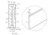
- FIG. 3 is a sectional view taken along line III-III in FIGS. 1 and 2.
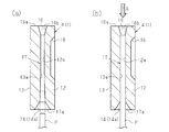
- (A), (b) is sectional drawing which shows an effect
- the bus bar 1 constitutes, for example, an electrode that is directly or indirectly connected to the DC power supply V, and is electrically connected to the plate-like electrode P of the inverter Inv. Function as.
- the bus bar 1 is made of a conductive metal material such as copper.
- the bus bar 1 is manufactured by metal powder injection molding using a metal powder containing copper powder as a material, so-called MIM.
- the bus bar 1 includes a rectangular parallelepiped main body 2 having a long side and a short side.
- first direction the longitudinal direction of the main body 2
- second direction the short direction of the main body 2
- first direction the direction orthogonal to the first direction and the second direction
- first direction the direction orthogonal to the first direction and the second direction
- first direction the direction orthogonal to the first direction and the second direction
- first direction the direction orthogonal to the first direction and the second direction
- the main body 2 has a thin plate shape in which the third direction is smaller than the second direction.
- the main body 2 has a pair of end portions 2a and 2b in the first direction, the end portion 2a is provided with a power supply side end portion 3, and the end portion 2b is provided with an electrode side end portion 4. Yes.
- the power supply side end 3 extends in the second direction from one end in the vicinity of the long side of the end 2 a of the main body 2.
- the power supply side end 3 has a thin plate shape having a thickness in the first direction and a width in the third direction.
- the electrode side end 4 is provided on the end 2 b opposite to the end 2 a of the main body 2.
- the electrode side end 4 extends in the first direction from one end of the short side of the main body 2.
- the electrode side end 4 has a cylindrical shape that bulges in the third direction.
- the power supply side end 3 is connected to a DC power supply V via a bolt or the like.
- the electrode side end 4 is electrically connected to the plate electrode P which is an electrode of the inverter Inv by laser welding.
- the electrode side end 4 is an example of a clamping part, and the plate electrode P of the inverter Inv is an example of a connection target.
- the electrode-side end 4 is provided with a peripheral wall W that forms an outline of the electrode-side end 4.
- the peripheral wall W includes a pair of side walls 12 and 13 facing in the third direction, a pair of end walls 14 and 15 connecting the side walls 12 and 13 at both side portions in the first direction, the side walls 12 and 13 and both end walls. And a bottom wall 16 connecting the fourteen and fifteen.
- the bottom wall 16 connects the side walls 12 and 13 and the both end walls 14 and 15 at one end in the second direction.
- a hollow portion 17 surrounded by the inner surface of the peripheral wall W is provided inside the electrode side end portion 4.
- the hollow portion 17 has an opening 17a and has a bottomed cylindrical shape having a depth in the second direction.
- the opening 17a opens in the direction opposite to the direction in which the power supply side end 3 extends.
- One side wall 12 of the side walls 12 and 13 (on the front side in FIG. 1 (back side in FIG. 2)) is provided with a recess 18 that is recessed inward from the outer surface of the electrode-side end 4. For this reason, the thickness (the size in the third direction) of the portion corresponding to the concave portion 18 of the side wall 12 is smaller than the thickness of other portions. The thickness of the part corresponding to the recess 18 of the side wall 12 is set smaller than the thickness of any part of the side wall 13.
- the outer surface 16a of the bottom wall 16 on the side opposite to the opening 17a is a flat surface parallel to the direction orthogonal to the depth direction of the hollow portion 17.
- One end surface constituting the long side of the main body 2 is flush with the outer surface 16 a of the bottom wall 16.
- the outer surface 16a of the bottom wall 16 is an example of a force acting part.
- a communication hole 16 b that communicates the inside and the outside of the bottom wall 16 is provided in the approximate center of the bottom wall 16.
- the opening area of the communication hole 16b is set smaller than the opening area of the opening 17a.
- the gap between the end walls 14 and 15, which is the size of the opening 17 a in the first direction, is set to be approximately the same (slightly larger) as the width of the plate electrode P.
- the facing surfaces 14 a and 15 a which are the inner surfaces of the end walls 14 and 15 are flat surfaces parallel to the depth direction of the hollow portion 17. Thereby, the clearance gap between the opposing surfaces 14a and 15a of the end walls 14 and 15 is maintained by the fixed magnitude
- the gap D1 between the side walls 12 and 13, which is the size of the opening 17a in the third direction, is the thickness D0 of the plate electrode P (shown in a virtual circle in the figure). It is set large compared.
- the facing surfaces 12 a and 13 a which are the inner surfaces of the side walls 12 and 13 are closest to each other at a portion corresponding to the concave portion 18 of the side wall 12 along the depth direction of the hollow portion 17.
- the opposing surfaces 12a and 13a are spaced apart toward each part corresponding to the opening 17a and the communication hole 16b.
- the gap D2 when the facing surfaces 12a and 13a are closest to each other is set slightly smaller than the thickness D0 of the plate electrode P. For this reason, between the opening part 17a and the site
- the plate electrode P is inserted into the hollow portion 17 (bus bar 1) of the electrode side end portion 4. Thereby, the plate electrode P is temporarily fixed to the bus bar 1.
- the electrode side end portion 4 is such that the longitudinal direction and the short direction of the opening 17 a of the hollow portion 17 coincide with the longitudinal direction and the short direction of the tip of the plate electrode P, respectively. It arrange
- the plate electrode P is inserted into the hollow portion 17.
- a worker or a work device presses the outer surface 16 a of the bottom wall 16 of the electrode side end 4 to generate a force necessary for inserting the plate electrode P into the hollow portion 17. That is, a force that opposes the insertion direction of the plate electrode P is generated.
- the plate-like electrode P is inserted into the hollow portion 17 until it reaches the bottom wall 16 from 17a.
- the opposing surfaces 12a and 13a of the side walls 12 and 13 are provided with plate-like electrodes P.
- the tip is abutted. Thereby, the position of the plate-like electrode P inserted into the electrode side end portion 4 is determined.
- the plate-like electrode P is moved to the electrode side end 4 while the tip of the plate electrode P moves on the opposing surfaces 12a, 13a of the side walls 12, 13.
- the electrode P is inserted.
- the plate electrode P is press-fitted in order from the tip thereof into a gap smaller than the thickness of the plate electrode P by the facing surfaces 12 a and 13 a of the side walls 12 and 13.
- the plate electrode P is inserted to the back of the hollow portion 17, and the plate electrode P is inserted.
- the opposing surfaces 12a and 13a of the side walls 12 and 13 of the hollow portion 17, particularly the portions corresponding to the concave portions 18 of the side walls 12 are sandwiched so as to clamp the plate electrode P from both sides. That is, the plate-like electrode P is sandwiched between the opposing surfaces 12 a and 13 a of the side walls 12 and 13. Thereby, the plate-like electrode P inserted into the electrode side end portion 4 (bus bar 1) is temporarily fixed and positioned.
- the worker or the working device looks at the state inside the hollow portion 17 from the communication hole 16 b of the bottom wall 16, and the plate-like electrode P extends to the back of the hollow portion 17. It is confirmed whether it has been inserted or whether the insertion of the plate electrode P has been completed.
- the preparation process is completed.
- the plate-like electrode P is sandwiched between the opposing surfaces 12 a and 13 a of the side walls 12 and 13 so that it does not fall off in the insertion direction. Temporarily fixed. Further, the plate-like electrode P is surrounded by the opposing surfaces 14a and 15a of the end walls 14 and 15, so that it does not rattle or swing in directions other than the insertion direction. Further, the plate electrode P does not advance further in the insertion direction due to the bottom wall 16. That is, after completion of the preparation process, the plate-like electrode P temporarily fixed to the electrode side end portion 4 (bus bar 1) can move only in the direction of falling off in the insertion direction. The movement of the plate electrode P in the direction other than the insertion direction is effectively restricted by the side walls 12, 13, the end walls 14, 15 and the bottom wall 16 constituting the hollow portion 17.
- the side wall 12 of the electrode side end portion 4 in the bus bar 1 is irradiated with laser light.
- the bus bar 1 and the plate-like electrode P are welded by the laser.
- the bus bar 1 and the plate-like electrode P after laser welding are melted around the recess 18 which is the laser light irradiation range.
- the periphery of the recess 18 is melted to form a laser welded portion, whereby the bus bar 1 and the plate electrode P are joined to each other.
- the plate electrode P is inserted into the hollow portion 17 of the electrode side end portion 4 of the bus bar 1.
- the plate-like electrode P is positioned relative to the bus bar 1 while being temporarily fixed to the bus bar 1.
- the function of temporarily fixing and positioning the plate-like electrode P on the bus bar 1 without a jig by the facing surfaces 12a and 13a of the side walls 12 and 13 constituting the outline of the electrode side end 4 is provided.
- FIG. 5A when the plate-like electrode P is inserted into the electrode side end 4 in the preparation step, the positioning of the connection target with respect to the opening 17a is assisted. Further, when the plate-like electrode P is inserted into the electrode-side end portion 4, the insertion of the tip of the plate-like electrode P is assisted by being guided by the opposing surfaces 12 a and 13 a of the side walls 12 and 13. In this case, insertion of the plate electrode P can be started with a relatively small force required when the plate electrode P is inserted. Thereby, the function for facilitating the operation
- the thickness of the concave portion 18 of the electrode side end 4 serving as a laser welded portion is smaller than the thickness of other portions. For this reason, at the time of laser welding, the energy of the laser beam is easily transmitted to the bus bar 1 and the plate electrode P. For this reason, the bus bar 1 and the plate electrode P are suitably melted. Thereby, the function for increasing the bonding strength between the bus bar 1 and the plate-like electrode P by laser welding can be added to the bus bar 1 by the recess 18 in the side wall 12 of the electrode side end 4.
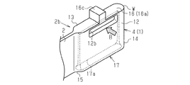
- one of the side walls 12 and 13 of the electrode side end portion 4 is provided with a communication hole 12 b that communicates the inside and the outside of the side wall 12. Yes. Further, the target portion 16 c protrudes from the bottom wall 16 in the depth direction of the hollow portion 17. The target portion 16c is provided on the outer surface 16a of the bottom wall 16 opposite to the opening portion 17a. The target portion 16c extends in the third direction so as to cross the outer surface 16a.
- the electrode side end portion 4 is electrically connected to the plate electrode P which is an electrode of the inverter Inv by TIG (TungstensInert Gas) welding (TIG welding) which is a kind of arc welding.
- TIG TungstensInert Gas
- TIG welding TungstensInert Gas welding
- the worker or the working device detects the state inside the hollow portion 17 through the communication hole 12 b of the side wall 12. As a result, when the plate electrode P is inserted deep into the hollow portion 17 and the insertion of the plate electrode P is completed, the preparation process is completed.
- the welding electrode is brought close to the bottom wall 16 of the electrode side end portion 4 of the bus bar 1 to connect the bus bar 1 and the plate electrode P to the TIG. Weld.
- the welding electrode 40a In TIG welding, the welding electrode 40a generates arc discharge in the bus bar 1 and the plate electrode P to be welded to melt the bus bar 1 and the plate electrode P. Thereby, the bus bar 1 and the plate electrode P are joined.
- the welding electrode 40 a is made of tungsten, and is connected to the welding power source 40.
- the welding power source 40 is connected to a power source (not shown).
- the bus bar 1 and the plate electrode P are arranged so as to generate arc discharge in the target portion 16c. The arc discharge is generated between the welding electrode 40a and the target portion 16c closest to the welding electrode 40a.
- the periphery of the target portion 16c which is an arc discharge generating portion, melts.
- the following actions and effects can be obtained in addition to the actions and effects of the first embodiment.
- the welding electrode 40 a As shown in FIG. 8, in the TIG welding process, among the bottom wall 16 of the electrode side end portion 4 serving as an arc welded portion, particularly in the target portion 16 c, it is easy to approach the welding electrode 40 a as compared with other portions. It is configured in shape. For this reason, when it welds by TIG welding, it becomes easy to produce arc discharge and the bus-bar 1 and the plate-shaped electrode P are fuse
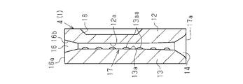
- the opposing surface 13 a of the side wall 13 where the recess 18 is not provided has a plurality of protrusions protruding from the opposing surface 13 a to the opposing surface 12 a. 13aa may be provided.
- the plate-like electrode P can be pressed against the side wall 12 irradiated with laser light during laser welding. Thereby, at the time of laser welding, the energy of a laser beam is more suitably transmitted to the bus bar 1 and the plate-like electrode P.
- a function for further increasing the bonding strength between the bus bar 1 and the plate electrode P by laser welding can be added to the bus bar 1 by the facing surface 13a (projection 13aa) of the side wall 13 of the electrode side end portion 4.
- the shape of the protrusion 13aa is arbitrary such as a circle or a square in plan view.
- the number of protrusions 13aa may be singular depending on the size and shape.
- the arrangement of the protrusions 13aa may be regular or irregular.
- electron beam welding may be employed instead of laser welding. It is known that electron beam welding generates a larger energy (heat) than laser welding. For this reason, in electron beam welding, an object having a larger thickness (difficult to transmit energy) than laser welding can also be an object to be welded. Therefore, in this modification, even if the recess 18 is not provided in the side wall 12, the same joining strength as in the case of laser welding may be ensured. Therefore, if the electron beam welding is employed, it is not essential to provide the recess 18 in the side wall 12, and the recess 18 may be omitted. However, as long as the strength of the side wall 12 (bus bar 1) can be ensured, the entire side wall 12 may be configured to be as thin as the concave portion 18. In this case, laser welding can be employed without providing the recess 18 in the side wall 12.
- the target portion 16c need not be provided on the bottom wall 16 if the arc discharge generation portion can be controlled from the relationship between the welding object and the welding electrode.
- the shape of the target part 16c protruded from the outer surface 16a of the bottom wall 16 is arbitrary, such as a cross-sectional round shape and a quadratic prism shape.
- the outer surface 16a of the bottom wall 16 should just be a shape which an operator and a working device can apply force, and may have unevenness other than flatness.
- the force acting portion may be provided on the side walls 12 and 13. If it is comprised so that force may be acted in the case of insertion of the plate-shaped electrode P to the electrode side edge part 4, it is not necessary to provide a force action part.
- the arrangement of the communication holes may be interchanged between the embodiments.
- the communication holes 12b and 16b may not be provided. In this case, the completion of the preparation process may be confirmed by applying a length for inserting the plate electrode P or a confirmation force.
- the shape of the connection target connected to the bus bar 1 is arbitrary, such as a round cross section or a square bar terminal.
- the outline of the electrode side end portion 4 and the shape of the hollow portion 17 may be changed according to the shape of the connection target.
- the peripheral wall W may be configured so that the outer periphery of the electrode side end portion 4 has a cylindrical shape.
- the inner surface of the peripheral wall W may be configured so that the hollow portion 17 has a cylindrical shape without changing the outline of the electrode side end portion 4.
- the rod-shaped terminal having a round cross section inserted into the electrode side end 4 only needs to be sandwiched between the inner surfaces of the peripheral walls W facing the terminal in the radial direction.
- the configuration of sandwiching the rod-shaped terminal having a round cross section may be continuous in the circumferential direction of the inner surface of the peripheral wall W, or may be discontinuous.
Landscapes
- Engineering & Computer Science (AREA)
- Physics & Mathematics (AREA)
- Plasma & Fusion (AREA)
- Mechanical Engineering (AREA)
- Optics & Photonics (AREA)
- Connections Effected By Soldering, Adhesion, Or Permanent Deformation (AREA)
- Butt Welding And Welding Of Specific Article (AREA)
- Laser Beam Processing (AREA)
Abstract
バスバーは、レーザー溶接部を介して板状電極と電気的に接続されることによって、導電体としての機能を果たす。また、バスバーは、有底筒状の電極側端部、すなわち、中空部を有している。電極側端部は、レーザー溶接部を介して板状電極と電気的に接続される前の準備工程で、板状電極の挿入を通じて、板状電極を挟持することができる。
Description
本発明は、バスバーに関する。
配線用材料として用いられるバスバーは、インバータ等の電極である接続対象と電気的に接続されることによって、導電体として機能する。バスバーは、例えば特許文献1に開示されるようにバスバーとは別に用意される電極接続具を用いて、接続対象と電気的に接続される。
特許文献1に記載の電極接続具は、インバータ等のパワーデバイスの板状電極と、接続用バスバーの板状電極とに対して、前記両板状電極の先端縁と側端縁とが一致するように重ね合わされた状態で、前記両板状電極の外周側から嵌合される。この場合、パワーデバイスと接続用バスバーとの各板状電極は、電極接続具で密着されることによって、互いに電気的に接続されている。
バスバーと接続対象とを電気的に接続する方法として、特許文献1に記載の電極接続具を用いる方法の他、バスバーと接続対象とを溶接によって電気的に接続する方法がある。ただし、バスバーと接続対象とを溶接する方法の場合、バスバーと接続対象とを溶接前に位置決めする必要がある。すなわち、溶接する場合であっても、特許文献1の電極接続具のような位置決め用治具を、バスバーとは別に用意しなければいけない。
本発明の目的は、バスバーと接続対象とを治具なしで溶接することのできるバスバーを提供することにある。
上記課題を解決するため、本発明の第一の態様によれば、溶接部を介して接続対象と電気的に接続されることによって、導電体としての機能を果たすバスバーが提供される。バスバーは、溶接部を介して接続対象と電気的に接続される前の状態で、接続対象の挿入を通じて、接続対象を挟持することのできる有底筒状の挟持部を有している。
(第1実施形態)
以下、バスバーの第1実施形態を説明する。
図1に示すように、バスバー1は、例えば、直流電源Vと直接的又は間接的に接続される電極を構成し、インバータInvの板状電極Pと電気的に接続されることによって、導電体として機能する。バスバー1は、銅等の導電性を有する金属材料からなる。バスバー1は、銅粉末を含む金属粉末を材料とした金属粉末射出成形、所謂、MIM(ミム)により、製造される。
以下、バスバーの第1実施形態を説明する。
図1に示すように、バスバー1は、例えば、直流電源Vと直接的又は間接的に接続される電極を構成し、インバータInvの板状電極Pと電気的に接続されることによって、導電体として機能する。バスバー1は、銅等の導電性を有する金属材料からなる。バスバー1は、銅粉末を含む金属粉末を材料とした金属粉末射出成形、所謂、MIM(ミム)により、製造される。
バスバー1は、長辺及び短辺を有する直方体状の本体部2を備えている。以下の説明で、本体部2の長手方向を「第1方向」と言い、本体部2の短手方向を「第2方向」と言い、第1方向及び第2方向に直交する方向を「第3方向」と言う。本体部2は、第2方向と比較して第3方向が小さい薄板状をなしている。本体部2は、第1方向に一対の端部2a,2bを有し、端部2aには、電源側端部3が設けられ、端部2bには、電極側端部4が設けられている。
電源側端部3は、本体部2の端部2aにおける長辺近傍の一端から、第2方向に延びている。電源側端部3は、第1方向に厚さを有し、第3方向に幅を有する薄板状をなしている。
電極側端部4は、本体部2の端部2aと反対側の端部2bに設けられている。電極側端部4は、本体部2の短辺の一端から第1方向に延びている。電極側端部4は、第3方向に膨出する筒状をなしている。
電源側端部3は、直流電源Vにボルト等を介して連結されている。電極側端部4は、レーザー溶接によって、インバータInvの電極である板状電極Pと電気的に接続される。電極側端部4は挟持部の一例であり、インバータInvの板状電極Pは接続対象の一例である。
次に、電極側端部4の構成について詳しく説明する。
図1及び図2に示すように、電極側端部4には、電極側端部4の外郭をなす周壁Wが設けられている。周壁Wは、第3方向に対向する一対の側壁12,13と、両側壁12,13を第1方向の両側部で連結する一対の端壁14,15と、両側壁12,13及び両端壁14,15を連結する底壁16とを有している。底壁16は、両側壁12,13及び両端壁14,15を第2方向の一方の端部で連結している。電極側端部4の内部には、周壁Wの内面によって囲まれた中空部17が設けられている。中空部17は、開口部17aを有し、第2方向に深さを有する有底筒状をなしている。開口部17aは、電源側端部3が延びる方向と反対方向に開口している。
図1及び図2に示すように、電極側端部4には、電極側端部4の外郭をなす周壁Wが設けられている。周壁Wは、第3方向に対向する一対の側壁12,13と、両側壁12,13を第1方向の両側部で連結する一対の端壁14,15と、両側壁12,13及び両端壁14,15を連結する底壁16とを有している。底壁16は、両側壁12,13及び両端壁14,15を第2方向の一方の端部で連結している。電極側端部4の内部には、周壁Wの内面によって囲まれた中空部17が設けられている。中空部17は、開口部17aを有し、第2方向に深さを有する有底筒状をなしている。開口部17aは、電源側端部3が延びる方向と反対方向に開口している。
側壁12,13のうち一方の側壁12(図1中、手前側(図2中、奥側))には、電極側端部4の外面から内側に凹んだ凹部18が設けられている。このため、側壁12の凹部18に対応する部位の厚さ(第3方向の大きさ)は、他の部位の厚さと比較して小さい。側壁12の凹部18に対応する部位の厚さは、側壁13の何れの部位の厚さよりも小さく設定されている。
開口部17aと反対側の底壁16の外面16aは、中空部17の深さ方向に直交する方向に対して平行な平坦面である。本体部2の長辺を構成する一方の端面は、底壁16の外面16aと面一である。底壁16の外面16aは、力作用部の一例である。
底壁16の略中央には、底壁16の内と外とを連通する連通孔16bが設けられている。連通孔16bの開口領域は、開口部17aの開口領域と比較して小さく設定されている。
ここで、中空部17の構成についてさらに詳しく説明する。
図2に示すように、開口部17aの第1方向の大きさである端壁14,15間の隙間は、板状電極Pの幅と略同一に(若干大きく)設定されている。また、端壁14,15の内面である対向面14a,15aは、中空部17の深さ方向に対して平行な平坦面である。これにより、端壁14,15の対向面14a,15a間の隙間は、開口部17aから連通孔16bまでの間で一定の大きさに維持されている。
図2に示すように、開口部17aの第1方向の大きさである端壁14,15間の隙間は、板状電極Pの幅と略同一に(若干大きく)設定されている。また、端壁14,15の内面である対向面14a,15aは、中空部17の深さ方向に対して平行な平坦面である。これにより、端壁14,15の対向面14a,15a間の隙間は、開口部17aから連通孔16bまでの間で一定の大きさに維持されている。
一方、図3に示すように、開口部17aの第3方向の大きさである側壁12,13間の隙間D1は、板状電極Pの厚さD0(図中、仮想円内に示す)と比較して大きく設定されている。また、側壁12,13の内面である対向面12a,13aは、中空部17の深さ方向に沿って、側壁12の凹部18に対応する部位において最も接近している。また、対向面12a,13aは、開口部17a及び連通孔16bに対応する各部位に向かうほど離間している。対向面12a,13aが最も接近したときの隙間D2は、板状電極Pの肉厚D0と比較して若干小さく設定されている。このため、開口部17aと側壁12の凹部18に対応する部位との間では、開口部17aに向かうほど、側壁12,13の対向面12a,13a間の隙間が大きくなる。
以下、バスバー1と板状電極Pとを溶接する工程について説明する。この工程には、実際の溶接前の準備工程と、実際に溶接するレーザー溶接工程との大きく2つの工程がある。
図4、図5(a)、及び図5(b)に示すように、準備工程では、電極側端部4の中空部17(バスバー1)に、板状電極Pを挿入する。これにより、バスバー1に板状電極Pを仮固定する。
図4に示すように、電極側端部4は、中空部17の開口部17aの長手方向及び短手方向と板状電極Pの先端の長手方向及び短手方向とがそれぞれ一致するように、板状電極Pと対向した状態で配置される。
そして、中空部17に、板状電極Pが挿入される。この場合、作業者や作業装置が、電極側端部4の底壁16の外面16aを押さえて、中空部17に板状電極Pを挿入するのに必要な力を発生させる。つまり、板状電極Pの挿入方向に対向する力を発生させる。この力によって、板状電極Pが17aから底壁16に達するまで、中空部17に挿入される。
具体的には、図5(a)に示すように、開口部17aと側壁12の凹部18に対応する部位との間では、側壁12,13の対向面12a,13aに、板状電極Pの先端が当接される。これにより、電極側端部4に挿入される板状電極Pの位置が決められる。
続いて、開口部17aと側壁12の凹部18に対応する部位との間では、側壁12,13の対向面12a,13aを板状電極Pの先端が移動しながら、電極側端部4に板状電極Pが挿入される。これにより、電極側端部4に対する板状電極Pの挿入が、無理なくガイドされる。このため、電極側端部4に対する板状電極Pの挿入が、比較的小さな力で実施される。
続いて、側壁12の凹部18に対応する部位では、側壁12,13の対向面12a,13aによる板状電極Pの厚さよりも小さい隙間に、板状電極Pがその先端から順に圧入される。
そして、図5(b)に示すように、底壁16の内面に板状電極Pの先端が達することで、中空部17の奥まで板状電極Pが挿入され、板状電極Pの挿入が完了する。この場合、中空部17の側壁12,13の対向面12a,13a、特に、側壁12の凹部18に対応する部位は、板状電極Pを両側から締め付けるようにして挟み込む。すなわち、板状電極Pは、側壁12,13の対向面12a,13aによって挟持される。これにより、電極側端部4(バスバー1)に挿入された板状電極Pが仮固定されるとともに、位置決めされる。
図5(b)の矢視Aで示すように、作業者や作業装置は、底壁16の連通孔16bから中空部17内部の状態を見て、中空部17の奥まで板状電極Pが挿入されたか、板状電極Pの挿入が完了しているか否かを確認する。中空部17の奥まで板状電極Pが挿入されたか、板状電極Pの挿入が完了している場合、準備工程が完了する。
また、図5(b)及び図6に示すように、準備工程の完了後、板状電極Pは、側壁12,13の対向面12a,13aに挟持されることによって、挿入方向に抜け落ちないように仮固定される。また、板状電極Pは、端壁14,15の対向面14a,15aに囲まれることによって、挿入方向以外の方向にがたつくこともなく、揺動することもない。また、板状電極Pは、底壁16によって、挿入方向にそれ以上は進まなくなる。すなわち、準備工程の完了後、電極側端部4(バスバー1)に仮固定された板状電極Pは、挿入方向に抜け落ちる方向にしか動くことがない。板状電極Pの挿入方向以外の方向への動きは、中空部17を構成する側壁12,13、端壁14,15、及び底壁16によって、効果的に規制されている。
図6に示すように、準備工程の完了後、レーザー溶接工程では、バスバー1における電極側端部4の側壁12に対してレーザー光を照射する。これにより、バスバー1と板状電極Pとがレーザーで溶接される。
レーザー溶接では、溶接対象であるバスバー1及び板状電極Pに、図示しない電源に接続されるレーザー発生源30のレーザー光のエネルギー(熱)を与える。その結果、バスバー1及び板状電極Pが溶融して接合される。バスバー1及び板状電極Pは、電極側端部4の側壁12の凹部18が設けられる範囲、すなわち、側壁12の厚さが小さい部位がレーザー光の照射範囲内に収まるようにそれぞれ配置される。そして、レーザー光を凹部18の一方の端から他方の端まで第1方向に移動させながら、凹部18の部位を溶融する。
レーザー溶接後のバスバー1及び板状電極Pは、レーザー光の照射範囲である凹部18周辺が溶融される。凹部18周辺が溶融されてレーザー溶接部が形成されることで、バスバー1と板状電極Pとが互いに接合される。
以上に説明した本実施形態によれば、以下に示す作用及び効果を奏する。
図5(b)に示すように、バスバー1と板状電極Pとの溶接前の準備工程において、板状電極Pは、バスバー1が有する電極側端部4の中空部17に挿入される。これによって、バスバー1に仮固定されると共に、板状電極Pは、バスバー1に対して位置決めもされる。これにより、電極側端部4の外郭を構成する側壁12,13の対向面12a,13aによって、治具なしでバスバー1に板状電極Pを仮固定するとともに位置決めするための機能を、バスバー1に付加することができる。すなわち、レーザー溶接工程では、バスバー1と板状電極Pとを治具なしで溶接することができる。
図5(b)に示すように、バスバー1と板状電極Pとの溶接前の準備工程において、板状電極Pは、バスバー1が有する電極側端部4の中空部17に挿入される。これによって、バスバー1に仮固定されると共に、板状電極Pは、バスバー1に対して位置決めもされる。これにより、電極側端部4の外郭を構成する側壁12,13の対向面12a,13aによって、治具なしでバスバー1に板状電極Pを仮固定するとともに位置決めするための機能を、バスバー1に付加することができる。すなわち、レーザー溶接工程では、バスバー1と板状電極Pとを治具なしで溶接することができる。
また、図5(a)に示すように、準備工程において、電極側端部4に板状電極Pを挿入する際、作業者や作業装置が、板状電極Pを挿入する際に必要な力を、底壁16の外面16aに発生させる。これにより、電極側端部4の底壁16の外面16aによって、電極側端部4に板状電極Pを挿入する作業を容易にするための機能を、バスバー1に付加することができる。
同じく、図5(a)に示すように、準備工程において、電極側端部4に板状電極Pを挿入する際、開口部17aに対する接続対象の位置決めが補助される。また、電極側端部4に板状電極Pを挿入する際、板状電極Pの先端の挿入が、側壁12,13の対向面12a,13aによりガイドされることで、補助される。この場合、板状電極Pを挿入する際に必要な力を比較的小さくして、板状電極Pの挿入を始めることができる。これにより、電極側端部4の側壁12,13の対向面12a,13aによって、挟持部に対して接続対象を挿入する作業を容易にするための機能を、バスバー1に付加することができる。
そして、図6に示すように、レーザー溶接工程において、レーザー溶接部となる電極側端部4の凹部18の厚さは、他の部位の厚さと比較して小さい。このため、レーザー溶接の際、レーザー光のエネルギーがバスバー1と板状電極Pとに伝達され易い。このため、バスバー1と板状電極Pとが好適に溶融される。これにより、電極側端部4の側壁12の凹部18によって、レーザー溶接によるバスバー1と板状電極Pとの接合強度を高めるための機能を、バスバー1に付加することができる。
(第2実施形態)
次に、バスバーの第2実施形態について説明する。既に説明した実施形態と同一構成などは、同一の符号を付すなどして、その重複する説明を省略する。
次に、バスバーの第2実施形態について説明する。既に説明した実施形態と同一構成などは、同一の符号を付すなどして、その重複する説明を省略する。
図7に示すように、電極側端部4の側壁12,13のうち一方の側壁12(図7、手前側)には、側壁12の内と外とを連通する連通孔12bが設けられている。
また、底壁16からは、ターゲット部16cが中空部17の深さ方向に突出している。ターゲット部16cは、開口部17aと反対側の底壁16の外面16aに設けられている。ターゲット部16cは、外面16aを横切るように第3方向に延びている。
また、底壁16からは、ターゲット部16cが中空部17の深さ方向に突出している。ターゲット部16cは、開口部17aと反対側の底壁16の外面16aに設けられている。ターゲット部16cは、外面16aを横切るように第3方向に延びている。
以下、バスバー1と板状電極Pとを溶接する工程について説明する。ここで、電極側端部4は、アーク溶接の一種であるTIG(Tungsten Inert Gas)溶接(ティグ溶接)によって、インバータInvの電極である板状電極Pと電気的に接続される。すなわち、第2実施形態の溶接する工程には、溶接前の準備工程と、溶接するTIG溶接工程との大きく2つの工程がある。
準備工程では、図7の矢視Bで示すように、作業者や作業装置が、側壁12の連通孔12bを通じて中空部17内部の状態を検出する。その結果、中空部17の奥まで板状電極Pが挿入されて、板状電極Pの挿入が完了している場合、準備工程が完了する。
図8に示すように、準備工程の完了後、TIG溶接工程では、バスバー1の電極側端部4の底壁16に溶接用電極を接近させることによって、バスバー1と板状電極PとをTIG溶接する。
TIG溶接では、溶接用電極40aが、溶接対象であるバスバー1及び板状電極Pにアーク放電を発生させて、バスバー1及び板状電極Pを溶融させる。これにより、バスバー1と板状電極Pとが接合される。溶接用電極40aは、タングステンからなり、溶接用電源40に接続されている。また、溶接用電源40は、図示しない電源に接続されている。バスバー1及び板状電極Pは、ターゲット部16cにアーク放電を発生させるように配置される。アーク放電は、溶接用電極40aと、溶接用電極40aに対して最も接近するターゲット部16cとの間に発生する。
TIG溶接後のバスバー1及び板状電極Pでは、アーク放電の発生部であるターゲット部16c周辺が溶融する。このため、ターゲット部16c周辺の部位が溶融してアーク溶接部が形成され、バスバー1と板状電極Pとがアーク溶接部を介して互いに接合される。
以上に説明した第2実施形態によれば、第1実施形態の作用及び効果に加えて、以下の作用及び効果を得ることができる。
図8に示すように、TIG溶接工程において、アーク溶接部となる電極側端部4の底壁16のうち、特にターゲット部16cでは、他の部位と比較して溶接用電極40aに接近し易い形状に構成されている。このため、TIG溶接によって溶接される際、アーク放電が生じ易くなり、バスバー1と板状電極Pとが好適に溶融される。これにより、電極側端部4の構成である底壁16のターゲット部16cによって、TIG溶接によるバスバー1と板状電極Pとの接合強度を高めるための機能を、バスバー1に付加することができる。
図8に示すように、TIG溶接工程において、アーク溶接部となる電極側端部4の底壁16のうち、特にターゲット部16cでは、他の部位と比較して溶接用電極40aに接近し易い形状に構成されている。このため、TIG溶接によって溶接される際、アーク放電が生じ易くなり、バスバー1と板状電極Pとが好適に溶融される。これにより、電極側端部4の構成である底壁16のターゲット部16cによって、TIG溶接によるバスバー1と板状電極Pとの接合強度を高めるための機能を、バスバー1に付加することができる。
上記各実施形態は、以下の形態にて実施することもできる。
・図9に示すように、第1実施形態において、側壁12,13のうち、凹部18が設けられていない側壁13の対向面13aには、対向面13aから対向面12aに突出する複数の突起13aaを設けてもよい。この場合、レーザー溶接の際にレーザー光が照射される側壁12に対して、板状電極Pを押し付けることができる。これにより、レーザー溶接の際、レーザー光のエネルギーがバスバー1と板状電極Pに、より好適に伝達される。これにより、電極側端部4の側壁13の対向面13a(突起13aa)によって、レーザー溶接によるバスバー1と板状電極Pとの接合強度をさらに高めるための機能を、バスバー1に付加することができる。突起13aaの形状は、平面視で丸や四角等、任意である。同様に、突起13aaの数は、大きさや形状によっては、単数であってもよい。同様に、突起13aaの配置は、規則的であっても、不規則的であってもよい。
・図9に示すように、第1実施形態において、側壁12,13のうち、凹部18が設けられていない側壁13の対向面13aには、対向面13aから対向面12aに突出する複数の突起13aaを設けてもよい。この場合、レーザー溶接の際にレーザー光が照射される側壁12に対して、板状電極Pを押し付けることができる。これにより、レーザー溶接の際、レーザー光のエネルギーがバスバー1と板状電極Pに、より好適に伝達される。これにより、電極側端部4の側壁13の対向面13a(突起13aa)によって、レーザー溶接によるバスバー1と板状電極Pとの接合強度をさらに高めるための機能を、バスバー1に付加することができる。突起13aaの形状は、平面視で丸や四角等、任意である。同様に、突起13aaの数は、大きさや形状によっては、単数であってもよい。同様に、突起13aaの配置は、規則的であっても、不規則的であってもよい。
・第1実施形態では、レーザー溶接に替えて、電子ビーム溶接を採用してもよい。電子ビーム溶接では、レーザー溶接と比較して大きいエネルギー(熱)が生じることが知られている。そのため、電子ビーム溶接では、レーザー溶接と比較して厚さの大きい(エネルギーが伝達され難い)物体も、溶接対象とすることができる。したがって、本変形例では、側壁12に凹部18を設けなくても、レーザー溶接の場合と同様の接合強度を確保できる場合がある。そのため、電子ビーム溶接を採用すれば、側壁12に凹部18を設けることは必須ではなく、凹部18は省略してもよい。ただし、側壁12(バスバー1)の強度が確保可能であれば、側壁12全体を、凹部18と同程度の薄さで構成してもよい。この場合、側壁12に凹部18を設けなくても、レーザー溶接を採用することができる。
・第2実施形態では、TIG溶接に替えて、抵抗溶接等、アーク放電を利用する溶接を採用してもよい。この場合であっても、第2実施形態に準じた作用及び効果を奏することができる。第2実施形態において、溶接対象と溶接電極との関係からアーク放電の発生部のコントロールが可能であれば、底壁16にターゲット部16cを設けなくてもよい。
・第2実施形態において、底壁16の外面16aから突出したターゲット部16cの形状は、断面丸形状や四角柱形状等、任意である。
・各実施形態において、側壁12,13の内面である対向面12a,13a間の隙間は、全体的に板状電極Pの厚さD0と比較して若干小さく設定してもよい。すなわち、側壁12,13の対向面12a,13a間の隙間は、開口部17aから連通孔16bの間で一定の大きさであってもよい。
・各実施形態において、側壁12,13の内面である対向面12a,13a間の隙間は、全体的に板状電極Pの厚さD0と比較して若干小さく設定してもよい。すなわち、側壁12,13の対向面12a,13a間の隙間は、開口部17aから連通孔16bの間で一定の大きさであってもよい。
・各実施形態において、底壁16の外面16aは、作業者や作業装置が力を加えることのできる形状であればよく、平坦以外に、凸凹を有していてもよい。また、力作用部を、側壁12,13に設けてもよい。電極側端部4への板状電極Pの挿入の際に力を作用させるように構成されていれば、力作用部は設けなくてもよい。
・各実施形態では、準備工程の完了を確認するための連通孔12b,16bの位置を、仕様等に合わせて変更してもよい。例えば、各実施形態の間で連通孔の配置を入れ替えてもよい。その他、連通孔12b,16bを設けなくてもよい。この場合、板状電極Pが挿入されている長さや確認用の力を作用させる等して、準備工程の完了を確認すればよい。
・各実施形態において、バスバー1に接続する接続対象の形状は、断面丸形状や四角棒状の端子等、任意である。この場合、接続対象の形状に合わせて、電極側端部4の外郭や中空部17の形状を変更してもよい。例えば、接続対象が断面丸形状の棒状の端子の場合、電極側端部4の外郭が円筒状をなすように、周壁Wを構成すればよい。その他、電極側端部4の外郭は変更せず、中空部17が円筒状をなすように周壁Wの内面を構成すればよい。この場合、電極側端部4に挿入された断面丸形状の棒状の端子は、端子の径方向に対向する周壁Wの内面に挟持されていればよい。断面丸形状の棒状の端子を挟持する構成は、周壁Wの内面の周方向に連続的であってもよく、非連続的であってもよい。
Claims (6)
- 溶接部を介して接続対象と電気的に接続されることによって、導電体としての機能を果たすバスバーにおいて、
前記溶接部を介して前記接続対象と電気的に接続される前の状態で、前記接続対象の挿入を通じて、前記接続対象を挟持することのできる有底筒状の挟持部を有する、バスバー。 - 前記挟持部には、前記挟持部の外郭をなす周壁が設けられ、
前記周壁の内面には、前記挟持部に挿入された状態の前記接続対象を挟み込む対向面が設けられている、請求項1に記載のバスバー。 - 前記挟持部には、前記挟持部に前記接続対象を挿入する際に力を作用させるための部位である力作用部が設けられている、請求項2に記載のバスバー。
- 前記挟持部は、前記挟持部に前記接続対象を挿入可能に開口する開口部を含み、
前記対向面間の隙間は、前記開口部に向かうほど大きくなる、請求項2又は3に記載のバスバー。 - 前記溶接部は、レーザー溶接部であって、
前記挟持部は、前記レーザー溶接部となる部位を含み、
前記レーザー溶接部となる部位の厚さは、前記挟持部の他の部位の厚さよりも小さい、請求項1~4のうちいずれか一項に記載のバスバー。 - 前記溶接部は、アーク溶接部であって、
前記挟持部は、前記アーク溶接部となる部位を含み、
前記アーク溶接部となる部位は、前記挟持部の他の部位と比較してアーク放電し易い形状を有している、請求項1~4のうちいずれか一項に記載のバスバー。
Applications Claiming Priority (2)
| Application Number | Priority Date | Filing Date | Title |
|---|---|---|---|
| JP2016184281A JP2018049736A (ja) | 2016-09-21 | 2016-09-21 | バスバー |
| JP2016-184281 | 2016-09-21 |
Publications (1)
| Publication Number | Publication Date |
|---|---|
| WO2018055962A1 true WO2018055962A1 (ja) | 2018-03-29 |
Family
ID=61689884
Family Applications (1)
| Application Number | Title | Priority Date | Filing Date |
|---|---|---|---|
| PCT/JP2017/029682 Ceased WO2018055962A1 (ja) | 2016-09-21 | 2017-08-18 | バスバー |
Country Status (2)
| Country | Link |
|---|---|
| JP (1) | JP2018049736A (ja) |
| WO (1) | WO2018055962A1 (ja) |
Citations (8)
| Publication number | Priority date | Publication date | Assignee | Title |
|---|---|---|---|---|
| JPH11297380A (ja) * | 1998-04-09 | 1999-10-29 | Harness Syst Tech Res Ltd | 電気接続箱のバスバー構造 |
| JP2000090992A (ja) * | 1998-09-17 | 2000-03-31 | Harness Syst Tech Res Ltd | バスバー溶接構造 |
| JP2005129498A (ja) * | 2003-10-01 | 2005-05-19 | Shindengen Electric Mfg Co Ltd | バスバーと導電部材との接続方法及び構造 |
| JP2006179197A (ja) * | 2004-12-20 | 2006-07-06 | Toyota Motor Corp | 電子機器用バスバー及び電子機器用バスバーへの接続端子の接合方法 |
| JP2010112266A (ja) * | 2008-11-06 | 2010-05-20 | Sanden Corp | インバータ一体型電動圧縮機 |
| EP2418736A1 (en) * | 2008-09-25 | 2012-02-15 | Fotios Messaritis | A method improving the electrical performance of the connections of the various elements in the electric power systems |
| JP2015231245A (ja) * | 2014-06-03 | 2015-12-21 | 株式会社ジェイテクト | バスバー、モータ制御装置およびモータ制御装置の組立方法 |
| JP2016058215A (ja) * | 2014-09-09 | 2016-04-21 | 三井化学株式会社 | 蓋体、電気素子、電気素子ユニット及び蓋体の製造方法 |
-
2016
- 2016-09-21 JP JP2016184281A patent/JP2018049736A/ja active Pending
-
2017
- 2017-08-18 WO PCT/JP2017/029682 patent/WO2018055962A1/ja not_active Ceased
Patent Citations (8)
| Publication number | Priority date | Publication date | Assignee | Title |
|---|---|---|---|---|
| JPH11297380A (ja) * | 1998-04-09 | 1999-10-29 | Harness Syst Tech Res Ltd | 電気接続箱のバスバー構造 |
| JP2000090992A (ja) * | 1998-09-17 | 2000-03-31 | Harness Syst Tech Res Ltd | バスバー溶接構造 |
| JP2005129498A (ja) * | 2003-10-01 | 2005-05-19 | Shindengen Electric Mfg Co Ltd | バスバーと導電部材との接続方法及び構造 |
| JP2006179197A (ja) * | 2004-12-20 | 2006-07-06 | Toyota Motor Corp | 電子機器用バスバー及び電子機器用バスバーへの接続端子の接合方法 |
| EP2418736A1 (en) * | 2008-09-25 | 2012-02-15 | Fotios Messaritis | A method improving the electrical performance of the connections of the various elements in the electric power systems |
| JP2010112266A (ja) * | 2008-11-06 | 2010-05-20 | Sanden Corp | インバータ一体型電動圧縮機 |
| JP2015231245A (ja) * | 2014-06-03 | 2015-12-21 | 株式会社ジェイテクト | バスバー、モータ制御装置およびモータ制御装置の組立方法 |
| JP2016058215A (ja) * | 2014-09-09 | 2016-04-21 | 三井化学株式会社 | 蓋体、電気素子、電気素子ユニット及び蓋体の製造方法 |
Also Published As
| Publication number | Publication date |
|---|---|
| JP2018049736A (ja) | 2018-03-29 |
Similar Documents
| Publication | Publication Date | Title |
|---|---|---|
| US8105712B2 (en) | Sealed secondary battery, and method for manufacturing the battery | |
| KR101418899B1 (ko) | 금속박의 중첩 접합 방법 및 접합 구조체 | |
| US8779321B2 (en) | Method of welding circuit conductor and terminal of control apparatus | |
| US11203085B2 (en) | Method and apparatus for laser welding | |
| JP7010720B2 (ja) | 抵抗スポット溶接方法 | |
| JPH11342477A (ja) | スポット溶接方法 | |
| WO2017110354A1 (ja) | シャント抵抗器の製造方法 | |
| JP2014136242A (ja) | 重ね溶接方法及び溶接構造体 | |
| JP2022512073A (ja) | エネルギー貯蔵セル、製造方法及びこの製造方法を実行するための装置 | |
| CN111001930A (zh) | 用于激光焊接的方法和设备 | |
| US20180079025A1 (en) | Dissimilar material joined body and dissimilar material joining method | |
| WO2015037652A1 (ja) | 抵抗スポット溶接方法および溶接構造物 | |
| WO2018055962A1 (ja) | バスバー | |
| JP2012252935A (ja) | 電力用半導体装置 | |
| JP2000246445A (ja) | めっき鋼板の溶接方法 | |
| JP5259152B2 (ja) | 電池セル、バッテリパックおよび電池セル製造方法 | |
| CN100467185C (zh) | 对焊装置及对焊方法 | |
| KR101608716B1 (ko) | 스폿 용접용 캡 팁 | |
| CN110653468B (zh) | 接合装置和接合方法 | |
| JPH1147925A (ja) | 板材の接合方法 | |
| US20050178745A1 (en) | Projection weld-bonding system and method | |
| EP3247009B1 (en) | Method for manufacturing tubular metal shell including ground electrode bar for spark plug, and method for manufacturing spark plug | |
| JP2021186841A (ja) | 接合物品の製造方法及び製造装置 | |
| JP5826305B2 (ja) | 制御装置の端子の溶接方法 | |
| KR100548015B1 (ko) | 전기저항용접용 전극부재 |
Legal Events
| Date | Code | Title | Description |
|---|---|---|---|
| 121 | Ep: the epo has been informed by wipo that ep was designated in this application |
Ref document number: 17852742 Country of ref document: EP Kind code of ref document: A1 |
|
| NENP | Non-entry into the national phase |
Ref country code: DE |
|
| 122 | Ep: pct application non-entry in european phase |
Ref document number: 17852742 Country of ref document: EP Kind code of ref document: A1 |