WO2018043041A1 - 誘電体多層膜付きガラス板の製造方法及び誘電体多層膜付きガラス板 - Google Patents
誘電体多層膜付きガラス板の製造方法及び誘電体多層膜付きガラス板 Download PDFInfo
- Publication number
- WO2018043041A1 WO2018043041A1 PCT/JP2017/028528 JP2017028528W WO2018043041A1 WO 2018043041 A1 WO2018043041 A1 WO 2018043041A1 JP 2017028528 W JP2017028528 W JP 2017028528W WO 2018043041 A1 WO2018043041 A1 WO 2018043041A1
- Authority
- WO
- WIPO (PCT)
- Prior art keywords
- film
- dielectric multilayer
- glass plate
- multilayer film
- flow rate
- Prior art date
- Legal status (The legal status is an assumption and is not a legal conclusion. Google has not performed a legal analysis and makes no representation as to the accuracy of the status listed.)
- Ceased
Links
Images
Classifications
-
- B—PERFORMING OPERATIONS; TRANSPORTING
- B32—LAYERED PRODUCTS
- B32B—LAYERED PRODUCTS, i.e. PRODUCTS BUILT-UP OF STRATA OF FLAT OR NON-FLAT, e.g. CELLULAR OR HONEYCOMB, FORM
- B32B9/00—Layered products comprising a layer of a particular substance not covered by groups B32B11/00 - B32B29/00
-
- C—CHEMISTRY; METALLURGY
- C03—GLASS; MINERAL OR SLAG WOOL
- C03C—CHEMICAL COMPOSITION OF GLASSES, GLAZES OR VITREOUS ENAMELS; SURFACE TREATMENT OF GLASS; SURFACE TREATMENT OF FIBRES OR FILAMENTS MADE FROM GLASS, MINERALS OR SLAGS; JOINING GLASS TO GLASS OR OTHER MATERIALS
- C03C17/00—Surface treatment of glass, not in the form of fibres or filaments, by coating
- C03C17/34—Surface treatment of glass, not in the form of fibres or filaments, by coating with at least two coatings having different compositions
-
- C—CHEMISTRY; METALLURGY
- C23—COATING METALLIC MATERIAL; COATING MATERIAL WITH METALLIC MATERIAL; CHEMICAL SURFACE TREATMENT; DIFFUSION TREATMENT OF METALLIC MATERIAL; COATING BY VACUUM EVAPORATION, BY SPUTTERING, BY ION IMPLANTATION OR BY CHEMICAL VAPOUR DEPOSITION, IN GENERAL; INHIBITING CORROSION OF METALLIC MATERIAL OR INCRUSTATION IN GENERAL
- C23C—COATING METALLIC MATERIAL; COATING MATERIAL WITH METALLIC MATERIAL; SURFACE TREATMENT OF METALLIC MATERIAL BY DIFFUSION INTO THE SURFACE, BY CHEMICAL CONVERSION OR SUBSTITUTION; COATING BY VACUUM EVAPORATION, BY SPUTTERING, BY ION IMPLANTATION OR BY CHEMICAL VAPOUR DEPOSITION, IN GENERAL
- C23C14/00—Coating by vacuum evaporation, by sputtering or by ion implantation of the coating forming material
- C23C14/06—Coating by vacuum evaporation, by sputtering or by ion implantation of the coating forming material characterised by the coating material
- C23C14/08—Oxides
-
- G—PHYSICS
- G02—OPTICS
- G02B—OPTICAL ELEMENTS, SYSTEMS OR APPARATUS
- G02B1/00—Optical elements characterised by the material of which they are made; Optical coatings for optical elements
- G02B1/10—Optical coatings produced by application to, or surface treatment of, optical elements
- G02B1/11—Anti-reflection coatings
- G02B1/113—Anti-reflection coatings using inorganic layer materials only
- G02B1/115—Multilayers
-
- G—PHYSICS
- G02—OPTICS
- G02B—OPTICAL ELEMENTS, SYSTEMS OR APPARATUS
- G02B5/00—Optical elements other than lenses
- G02B5/20—Filters
- G02B5/26—Reflecting filters
-
- G—PHYSICS
- G02—OPTICS
- G02B—OPTICAL ELEMENTS, SYSTEMS OR APPARATUS
- G02B5/00—Optical elements other than lenses
- G02B5/20—Filters
- G02B5/28—Interference filters
Definitions
- the present invention relates to a method for producing a glass plate with a dielectric multilayer film in which a dielectric multilayer film is provided on the glass plate, and a glass plate with a dielectric multilayer film.
- the dielectric multilayer film is used as a functional film such as an antireflection film.
- Patent Document 1 discloses a glass plate with a dielectric multilayer film as an infrared shielding glass.
- Patent Document 1 describes a multilayer film in which a tantalum oxide film, a nitride film, and a tantalum oxide film are stacked in this order as a dielectric multilayer film.
- Patent Document 2 discloses a glass plate with a dielectric multilayer film as a heat ray shielding glass.
- a dielectric multilayer film is laminated on a glass substrate provided with a heat ray shielding film.
- a multilayer film in which a first transparent protective film such as silicon nitride and a second transparent protective film such as zirconium oxide are laminated in this order is used.
- Patent Document 1 a dielectric multilayer film is formed on a glass plate by sputtering.
- Patent Document 1 and Patent Document 2 when a glass plate with a dielectric multilayer film obtained by sputtering is combined with other parts to produce a final product such as an electronic part, the film surface is scratched. There was a thing. That is, the glass plates with dielectric multilayer films of Patent Document 1 and Patent Document 2 were not sufficiently scratch resistant.
- An object of the present invention is to provide a method for producing a glass plate with a dielectric multilayer film and a glass plate with a dielectric multilayer film, which are excellent in scratch resistance.
- a manufacturing method of a glass plate with a dielectric multilayer film according to the present invention includes a glass plate and a dielectric multilayer film laminated on the glass plate, and the dielectric multilayer film is made of silicon oxide.
- a method for producing a glass plate with a dielectric multilayer film comprising: a first film having a refractive index higher than that of silicon oxide; and the glass sheet is prepared. And a step of forming the dielectric multilayer film on the glass plate by sputtering, and when forming the first film by sputtering, a film forming pressure of the first film is set. It is characterized by being 0.4 Pa or less.
- the first film and the second film are alternately laminated.
- the film formation pressure of the first film is 0.12 Pa or more.
- the film formation pressure of the second film is set to 0.4 Pa or less.
- the second film is made of tantalum oxide.
- the dielectric multilayer film is an antireflection film.
- the dielectric multilayer film may be an infrared reflective film.
- a glass plate with a dielectric multilayer film according to the present invention includes a glass plate and a dielectric multilayer film laminated on the glass plate, wherein the dielectric multilayer film is made of silicon oxide. And the outermost layer of the dielectric multilayer film is the second film, and JIS K 5600-5-4 of the dielectric multilayer film: The pencil hardness measured according to 1999 is 3H or more.
- the present invention it is possible to provide a method for producing a glass plate with a dielectric multilayer film and a glass plate with a dielectric multilayer film, which are excellent in scratch resistance.
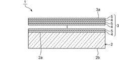
- FIG. 1 is a schematic cross-sectional view showing a glass plate with a dielectric multilayer film obtained by the method for manufacturing a glass plate with a dielectric multilayer film according to an embodiment of the present invention.
- FIG. 1 is a schematic cross-sectional view showing a glass plate with a dielectric multilayer film obtained by the method for manufacturing a glass plate with a dielectric multilayer film according to an embodiment of the present invention.
- a glass plate 1 with a dielectric multilayer film includes a glass plate 2 and a dielectric multilayer film 3.
- the glass plate 2 has a first main surface 2a and a second main surface 2b facing each other.
- a dielectric multilayer film 3 is provided on the first main surface 2a of the glass plate 2.
- the dielectric multilayer film 3 may also be provided on the second main surface 2b. That is, the dielectric multilayer film 3 may be provided only on one main surface of the first main surface 2a and the second main surface 2b, or provided on both main surfaces. May be.
- the dielectric multilayer film 3 includes a first film 4 and a second film 5.
- the first film 4 is made of silicon oxide.
- the second film 5 is composed of a film having a refractive index higher than that of silicon oxide.
- the dielectric multilayer film 3 has a configuration in which the first films 4 and the second films 5 are alternately stacked one by one. More specifically, the first film 4 is laminated on the first main surface 2a of the glass plate 2, and the second film 5 and the first film 4 are alternately laminated on the first film 4 one by one. The outermost layer is the second film 5. With such a configuration, the dielectric multilayer film 3 has an antireflection function. In the present invention, the dielectric multilayer film 3 may be another functional film such as an infrared reflecting film. The dielectric multilayer film 3 may have an antireflection function and an infrared reflection function.
- the number of layers constituting the dielectric multilayer film 3 is ten.
- the number of layers constituting the dielectric multilayer film 3 is not particularly limited.
- the number of layers of the dielectric multilayer film 3 is preferably 4 or more, and preferably 50 or less. When the number of layers of the film constituting the dielectric multilayer film 3 is within the above range, it is possible to obtain higher optical characteristics while having higher scratch resistance.
- the second film 5 is disposed on the outermost surface 3a side of the dielectric multilayer film 3.
- the first film 4 may be disposed on the outermost surface 3a side of the dielectric multilayer film 3, but the first film 4 is disposed on the outermost surface 3a side of the dielectric multilayer film 3 as in the present embodiment.
- 2 membranes 5 are preferably arranged.
- tantalum oxide is used as the material constituting the second film 5
- the chemical resistance of the glass plate 1 with the dielectric multilayer film is further increased by arranging the second film 5 on the outermost surface 3 a side. Can be increased.
- the dielectric multilayer film 3 preferably has a pencil hardness of 3H or more measured according to JIS K 5600-5-4: 1999. Thereby, it has much more sufficient abrasion resistance.
- the pencil hardness is more preferably 4H or more, and further preferably 6H or more.
- Glass plate examples of the glass constituting the glass plate include SiO 2 —B 2 O 3 —RO (R is Mg, Ca, Sr or Ba) -based glass, SiO 2 —B 2 O 3 —R ′ 2 O (R ′ is Li, Na or Ka) glass, SiO 2 —B 2 O 3 —RO—R ′ 2 O (R ′ is Li, Na or Ka) glass, SnO—P 2 O 5 glass, TeO 2 glass or Bi 2 O 3 glass or the like can be used.
- the thickness of the glass plate is not particularly limited, but can be, for example, 40 ⁇ m to 1200 ⁇ m.
- the dielectric multilayer film has the following first film and second film.
- the first film is made of silicon oxide.
- the film thickness per layer of the first film is not particularly limited, but the lower limit value of the film thickness is preferably 1.5 nm or more, more preferably 2 nm or more, and the upper limit value of the film thickness is Preferably it is 200 nm or less, More preferably, it is 150 nm or less.
- the film thickness per layer of the first film is equal to or greater than the above lower limit value, more optimal optical characteristics can be obtained.
- the film thickness per layer of the first film is not more than the above upper limit value, it is possible to obtain more optimal optical characteristics while further shortening the film formation time.
- the second film is made of a material having a refractive index higher than that of silicon oxide.
- the material having a refractive index higher than that of silicon oxide is not particularly limited.
- tantalum oxide, niobium oxide, titanium oxide, hafnium oxide, silicon nitride, zirconium oxide, or the like can be used. These materials may be used alone or in combination.
- the second film 5 of the second, fourth, and sixth layers from the glass plate 2 side in FIG. 1 is made of niobium oxide, and the eighth and tenth layers from the glass plate 2 side.
- the second film 5 of the eye may be made of tantalum oxide. Tantalum oxide is preferably used as a material for forming a film having a higher refractive index than silicon oxide from the viewpoint of making the film surface less susceptible to scratches and further improving the scratch resistance.
- the film thickness per layer of the second film is not particularly limited, but the lower limit value of the film thickness is preferably 1.5 nm or more, more preferably 2 nm or more, and the upper limit value of the film thickness is Preferably it is 200 nm or less, More preferably, it is 150 nm or less.
- the film thickness per layer of the second film is equal to or more than the above lower limit value, more optimal optical characteristics can be obtained.
- the film thickness per layer of the second film is not more than the above upper limit value, it is possible to obtain more optimal optical characteristics while having more sufficient strength.
- the glass plate 2 is prepared. Subsequently, the prepared glass plate 2 is set in a sputtering apparatus. In the sputtering, the temperature of the glass plate 2 is preferably 50 ° C. to 150 ° C., for example.
- a silicon target and a metal target capable of forming a film having a higher refractive index than silicon oxide are prepared.
- the silicon target is a target for forming the first film 4.
- a metal target capable of forming a film having a higher refractive index than silicon oxide is a target for forming the second film 5.
- a target such as tantalum, niobium, titanium, hafnium, or zirconium can be used. Among these, it is preferable to use a tantalum target from the viewpoint of further increasing the strength of the obtained film.
- a mixed gas of an inert gas and an oxygen gas is introduced into the sputtering apparatus, a silicon target is sputtered, and the first film 4 is formed on the glass plate 2.
- the deposition pressure of the first film 4 is 0.4 Pa or less.
- the inert gas nitrogen gas, argon gas, or a mixed gas of argon gas and nitrogen gas can be used.
- it is a mixed gas of argon gas and nitrogen gas.
- the mixed gas of the inert gas and the oxygen gas is desirably introduced after the inside of the sputtering apparatus is evacuated by a vacuum pump or the like.
- the mixing ratio of the inert gas and the oxygen gas is not particularly limited, and can be, for example, in the range of 2: 1 to 8: 1.
- the second film 5 is formed on the first film 4 by sputtering a metal target capable of forming a film having a higher refractive index than silicon oxide.
- the board 1 can be obtained.
- the feature of the manufacturing method of the present embodiment is that the film forming pressure when forming the first film 4 is 0.4 Pa or less.
- silicon (silicon oxide) can be deposited without lowering the energy of silicon (silicon oxide) knocked out in the state of atoms or molecules, a dense film can be obtained. Therefore, in the manufacturing method of this embodiment, the hardness of the dielectric multilayer film 3 can be increased, and the film surface of the obtained glass plate 1 with a dielectric multilayer film can be made difficult to be damaged. Therefore, the obtained glass plate 1 with a dielectric multilayer film is excellent in scratch resistance.
- the film formation pressure of the first film 4 is preferably 0.3 Pa or less, and preferably 0.25 Pa or less. More preferred.
- the film formation pressure of the first film 4 is preferably 0.12 Pa or more, and more preferably 0.15 Pa or more. In this case, film peeling of the first film 4 can be made more difficult to occur, and the number of pinholes can be further reduced.
- the film formation pressure of the second film 5 is preferably 0.4 Pa or less, more preferably 0.25 Pa or less, and further preferably 0.15 Pa or less.
- the film surface of the obtained glass plate 1 with a dielectric multilayer film can be made more difficult to be scratched, and the scratch resistance of the glass plate 1 with a dielectric multilayer film can be further enhanced.
- the lower limit value of the film formation pressure of the second film 5 is not particularly limited, but is preferably 0.05 Pa or more from the viewpoint of forming the second film 5 more reliably.
- Example 1 First, a glass plate was prepared. Subsequently, the prepared glass plate was set in a sputtering apparatus. Next, a mixed gas of argon gas and oxygen gas was introduced into the sputtering apparatus, a silicon target was sputtered, and a silicon oxide (SiO 2 ) film was formed on the glass plate. At this time, the flow rate of argon gas was 300 sccm, and the flow rate of oxygen gas was 120 sccm. The deposition pressure of the SiO 2 film was 0.3 Pa.
- a tantalum oxide (Ta 2 O 5 ) film was formed on the SiO 2 film by sputtering a tantalum target while maintaining a mixed gas of argon gas and oxygen gas at the same flow rate.
- the deposition pressure of the Ta 2 O 5 film was 0.3 Pa.
- a glass plate with a dielectric multilayer film having a total of 18 layers in which SiO 2 films and Ta 2 O 5 films are alternately laminated one by one on the glass plate 2 is obtained. Obtained.
- the outermost layer was a Ta 2 O 5 film. Further, only when forming the outermost Ta 2 O 5 film, the flow rate of argon gas was 100 sccm, the flow rate of oxygen gas was 40 sccm, and the deposition pressure was 0.1 Pa.
- Examples 2 to 7 Implemented except that the flow rates of argon gas and oxygen gas were changed as shown below, and the film forming pressure when forming the SiO 2 film and Ta 2 O 5 film was changed as shown in Table 1 below.
- a glass plate with a dielectric multilayer film was obtained in the same manner as in Example 1.
- the flow rate of argon gas (argon flow rate) and the flow rate of oxygen gas (oxygen flow rate) are as follows when forming the SiO 2 film and when forming the Ta 2 O 5 film: Changed as shown.
- Example 2 Argon flow rate: 100 sccm, oxygen flow rate: 40 sccm
- Example 3 Argon flow rate: 150 sccm, oxygen flow rate: 60 sccm
- Example 4 Argon flow rate: 200 sccm, oxygen flow rate: 80 sccm
- Example 2 SiO 2 film Argon flow rate: 100 sccm, oxygen flow rate: 40 sccm Ta 2 O 5 film of Example 5: Argon flow rate: 300 sccm, oxygen flow rate: 120 sccm SiO 2 film of Example 6
- Example 7 SiO 2 film Argon flow rate: 200 sccm, oxygen flow rate: 80 sccm Ta 2 O 5 film of Example 7: Argon flow rate: 100 sccm, oxygen flow rate: 40
- Example 8 The number of laminated dielectric multilayer films was changed to 17 layers, the outermost layer was changed to a SiO 2 film (the outermost layer material was SiO 2 ), and the deposition pressure of the outermost SiO 2 film was changed to the following Table 1.
- Pencil hardness The pencil hardness was measured according to JIS K 5600-5-4: 1999. In addition, the presence or absence of the scar at the time of determining pencil hardness was expanded and magnified by 500 times with the optical microscope, and was observed.
- the number of pinholes having a diameter of 8 ⁇ m or more present per 0.028 m 2 of the outermost surface area of the dielectric multilayer was evaluated.
- the glass plate with a dielectric multilayer film was immersed in 3% by mass of EC500 (manufactured by Henkel Japan) at 60 ° C. for 800 seconds, and then immersed in a 3% by mass of NaOH solution at 60 ° C. for 60 seconds.
- the transmittance of the glass plate with a dielectric multilayer film before and after immersion in EC500 and NaOH solution was measured by Hitachi High-Tech, product name “U-4000”, and chemical resistance was evaluated using the following evaluation criteria. did.
Landscapes
- Physics & Mathematics (AREA)
- Chemical & Material Sciences (AREA)
- General Physics & Mathematics (AREA)
- Optics & Photonics (AREA)
- Organic Chemistry (AREA)
- Chemical Kinetics & Catalysis (AREA)
- Engineering & Computer Science (AREA)
- Materials Engineering (AREA)
- Mechanical Engineering (AREA)
- Metallurgy (AREA)
- Inorganic Chemistry (AREA)
- Life Sciences & Earth Sciences (AREA)
- General Chemical & Material Sciences (AREA)
- Geochemistry & Mineralogy (AREA)
- Surface Treatment Of Glass (AREA)
- Laminated Bodies (AREA)
- Optical Filters (AREA)
- Surface Treatment Of Optical Elements (AREA)
- Physical Vapour Deposition (AREA)
Abstract
耐擦傷性に優れる、誘電体多層膜付きガラス板の製造方法を提供する。 ガラス板2と、ガラス板2上に積層されている誘電体多層膜3とを備え、誘電体多層膜3が、酸化ケイ素により構成されている第1の膜4と、酸化ケイ素より屈折率の高い材料により構成されている第2の膜5とを有する、誘電体多層膜付きガラス板1を製造する方法であって、ガラス板2を用意する工程と、ガラス板2上に、スパッタリングにより誘電体多層膜3を成膜する工程と、を備え、スパッタリングにより第1の膜4を成膜するに際し、第1の膜4の成膜圧力を0.4Pa以下とすることを特徴としている。
Description
本発明は、ガラス板上に誘電体多層膜が設けられた、誘電体多層膜付きガラス板の製造方法及び誘電体多層膜付きガラス板に関するものである。
従来、ガラス板上に誘電体多層膜が設けられた、誘電体多層膜付きガラス板が用いられている。上記誘電体多層膜は、反射防止膜などの機能膜として利用されている。
例えば、下記の特許文献1には、赤外線遮断ガラスとしての誘電体多層膜付きガラス板が開示されている。特許文献1では、誘電体多層膜として、酸化タンタル膜、窒化物膜及び酸化タンタル膜がこの順に積層されてなる多層膜が記載されている。
また、下記の特許文献2には、熱線遮蔽ガラスとしての誘電体多層膜付きガラス板が開示されている。特許文献2では、熱線遮蔽膜が設けられたガラス基板上に、誘電体多層膜が積層されている。誘電体多層膜としては、窒化ケイ素などの第1の透明保護膜と、酸化ジルコニウムなどの第2の透明保護膜とがこの順に積層されてなる多層膜が用いられている。
特許文献1及び特許文献2では、ガラス板上に、スパッタリングにより誘電体多層膜が形成されている。
しかしながら、特許文献1や特許文献2のように、スパッタリングにより得られた誘電体多層膜付きガラス板では、他の部品と組み合わせて電子部品などの最終製品を製造するに際し、膜面に傷が生じることがあった。すなわち、特許文献1や特許文献2の誘電体多層膜付きガラス板は、耐擦傷性が十分でなかった。
本発明の目的は、耐擦傷性に優れる、誘電体多層膜付きガラス板の製造方法及び誘電多層膜付きガラス板を提供することにある。
本発明に係る誘電体多層膜付きガラス板の製造方法は、ガラス板と、前記ガラス板上に積層されている誘電体多層膜とを備え、前記誘電体多層膜が、酸化ケイ素により構成されている第1の膜と、前記酸化ケイ素より屈折率の高い材料により構成されている第2の膜とを有する、誘電体多層膜付きガラス板を製造する方法であって、前記ガラス板を用意する工程と、前記ガラス板上に、スパッタリングにより前記誘電体多層膜を成膜する工程と、を備え、前記スパッタリングにより前記第1の膜を成膜するに際し、前記第1の膜の成膜圧力を0.4Pa以下とすることを特徴としている。
本発明に係る誘電体多層膜付きガラス板の製造方法では、好ましくは、前記誘電体多層膜において、前記第1の膜と前記第2の膜とが交互に積層されている。
本発明に係る誘電体多層膜付きガラス板の製造方法では、好ましくは、前記第1の膜の前記成膜圧力を、0.12Pa以上とする。
本発明に係る誘電体多層膜付きガラス板の製造方法では、好ましくは、前記スパッタリングにより前記第2の膜を成膜するに際し、前記第2の膜の成膜圧力を、0.4Pa以下とする。
本発明に係る誘電体多層膜付きガラス板の製造方法では、好ましくは、前記第2の膜が、酸化タンタルにより構成されている。
本発明に係る誘電体多層膜付きガラス板の製造方法では、好ましくは、前記誘電体多層膜が、反射防止膜である。
本発明に係る誘電体多層膜付きガラス板の製造方法では、前記誘電体多層膜が、赤外線反射膜であってもよい。
本発明に係る誘電多層膜付きガラス板は、ガラス板と、前記ガラス板上に積層されている誘電体多層膜とを備え、前記誘電体多層膜が、酸化ケイ素により構成されている第1の膜と、酸化タンタルにより構成されている第2の膜とを有し、前記誘電体多層膜の最外層は前記第2の膜であり、前記誘電体多層膜のJIS K 5600-5-4:1999に準拠して測定した鉛筆硬度が3H以上であることを特徴とする。
本発明によれば、耐擦傷性に優れる、誘電体多層膜付きガラス板の製造方法及び誘電多層膜付きガラス板を提供することができる。
以下、好ましい実施形態について説明する。但し、以下の実施形態は単なる例示であり、本発明は以下の実施形態に限定されるものではない。また、各図面において、実質的に同一の機能を有する部材は同一の符号で参照する場合がある。
図1は、本発明の一実施形態に係る誘電体多層膜付きガラス板の製造方法により得られる誘電体多層膜付きガラス板を示す模式的断面図である。
図1に示すように、誘電体多層膜付きガラス板1は、ガラス板2及び誘電体多層膜3を備える。ガラス板2は、互いに対向している第1の主面2a及び第2の主面2bを有する。ガラス板2の第1の主面2a上には、誘電体多層膜3が設けられている。なお、誘電体多層膜3は、第2の主面2b上にも設けられていてもよい。すなわち、誘電体多層膜3は、第1の主面2a及び第2の主面2bのうち一方側の主面上にのみに設けられていてもよいし、両側の主面上に設けられていてもよい。
誘電体多層膜3は、第1の膜4及び第2の膜5を有する。第1の膜4は、酸化ケイ素により構成されている。他方、第2の膜5は、酸化ケイ素より屈折率の高い膜により構成されている。
本実施形態において、誘電体多層膜3は、第1の膜4と、第2の膜5とが1層ずつ交互に積層された構成である。より具体的には、ガラス板2の第1の主面2a上に、第1の膜4が積層されており、その上に第2の膜5及び第1の膜4が1層ずつ交互に積層されており、最外層は第2の膜5である。このような構成により、誘電体多層膜3は反射防止機能を有する。本発明において、誘電体多層膜3は、赤外線反射膜などの他の機能膜であってもよい。また、誘電体多層膜3は、反射防止機能及び赤外線反射機能を有してもよい。
本実施形態においては、誘電体多層膜3を構成する膜の層数が10層である。もっとも、本発明において、誘電体多層膜3を構成する膜の層数は、特に限定されない。誘電体多層膜3を構成する膜の層数は、好ましくは4層以上であり、好ましくは、50層以下である。誘電体多層膜3を構成する膜の層数が、上記範囲内にある場合、より一層高い耐擦傷性を有しつつ、より一層高い光学特性を得ることができる。
また、本実施形態においては、誘電体多層膜3の最表面3a側に第2の膜5が配置されている。もっとも、本発明においては、誘電体多層膜3の最表面3a側に第1の膜4が配置されていてもよいが、本実施形態のように誘電体多層膜3の最表面3a側に第2の膜5が配置されていることが好ましい。特に、第2の膜5を構成する材料として、酸化タンタルを用いる場合、第2の膜5を最表面3a側に配置することで、誘電体多層膜付きガラス板1の耐薬品性をより一層高めることができる。
また、本実施形態において、誘電体多層膜3は、JIS K 5600-5-4:1999に準拠して測定した鉛筆硬度が3H以上であることが好ましい。これにより、より一層十分な耐擦傷性を有する。鉛筆硬度は、4H以上であることがより好ましく、6H以上であることがさらに好ましい。
以下、本発明の誘電体多層膜付きガラス板を構成する各材料について、より詳細に説明する。
(ガラス板)
ガラス板を構成するガラスとしては、例えば、SiO2-B2O3-RO(RはMg、Ca、SrまたはBa)系ガラス、SiO2-B2O3-R’2O(R’はLi、NaまたはKa)系ガラス、SiO2-B2O3-RO-R’2O(R’はLi、NaまたはKa)系ガラス、SnO-P2O5系ガラス、TeO2系ガラス又はBi2O3系ガラスなどを用いることができる。
ガラス板を構成するガラスとしては、例えば、SiO2-B2O3-RO(RはMg、Ca、SrまたはBa)系ガラス、SiO2-B2O3-R’2O(R’はLi、NaまたはKa)系ガラス、SiO2-B2O3-RO-R’2O(R’はLi、NaまたはKa)系ガラス、SnO-P2O5系ガラス、TeO2系ガラス又はBi2O3系ガラスなどを用いることができる。
ガラス板の厚みとしては、特に限定されないが、例えば、40μm~1200μmとすることができる。
(誘電体多層膜)
誘電体多層膜は、以下の第1の膜及び第2の膜を有する。
誘電体多層膜は、以下の第1の膜及び第2の膜を有する。
(第1の膜)
第1の膜は、酸化ケイ素により構成されている。
第1の膜は、酸化ケイ素により構成されている。
第1の膜の1層あたりの膜厚としては、特に限定されないが、膜厚の下限値は、好ましくは1.5nm以上であり、より好ましくは2nm以上であり、膜厚の上限値は、好ましくは200nm以下であり、より好ましくは150nm以下である。
第1の膜の1層当たりの膜厚が、上記の下限値以上である場合、より一層最適な光学特性を得ることができる。一方、第1の膜の1層当たりの膜厚が、上記の上限値以下である場合、成膜時間をより一層短縮しつつ、より一層最適な光学特性を得ることができる。
(第2の膜)
第2の膜は、酸化ケイ素より屈折率が高い材料により構成されている。酸化ケイ素より屈折率が高い材料としては、特に限定されないが、例えば、酸化タンタルや酸化ニオブ、酸化チタン、酸化ハフニウム、窒化シリコン、酸化ジルコニウムなどを用いることができる。これらの材料は、単独で用いてもよく、複数を併用してもよい。より具体的には、図1のガラス板2側から2層目、4層目及び6層目の第2の膜5は、酸化ニオブにより構成され、ガラス板2側から8層目及び10層目の第2の膜5は、酸化タンタルにより構成されていてもよい。膜面により一層傷を入り難くし、耐擦傷性をより一層高める観点からは、酸化ケイ素より屈折率が高い膜を構成する材料として、酸化タンタルを用いることが好ましい。
第2の膜は、酸化ケイ素より屈折率が高い材料により構成されている。酸化ケイ素より屈折率が高い材料としては、特に限定されないが、例えば、酸化タンタルや酸化ニオブ、酸化チタン、酸化ハフニウム、窒化シリコン、酸化ジルコニウムなどを用いることができる。これらの材料は、単独で用いてもよく、複数を併用してもよい。より具体的には、図1のガラス板2側から2層目、4層目及び6層目の第2の膜5は、酸化ニオブにより構成され、ガラス板2側から8層目及び10層目の第2の膜5は、酸化タンタルにより構成されていてもよい。膜面により一層傷を入り難くし、耐擦傷性をより一層高める観点からは、酸化ケイ素より屈折率が高い膜を構成する材料として、酸化タンタルを用いることが好ましい。
第2の膜の1層あたりの膜厚としては、特に限定されないが、膜厚の下限値は、好ましくは1.5nm以上であり、より好ましくは2nm以上であり、膜厚の上限値は、好ましくは200nm以下であり、より好ましくは150nm以下である。
第2の膜の1層当たりの膜厚が、上記の下限値以上である場合、より一層最適な光学特性を得ることができる。一方、第2の膜の1層当たりの膜厚が、上記の上限値以下である場合、より一層十分な強度を有しつつ、より一層最適な光学特性を得ることができる。
以下、誘電体多層膜付きガラス板1の一例としての製造方法について、詳細に説明する。
(製造方法)
まず、ガラス板2を用意する。続いて、用意したガラス板2をスパッタリング装置にセットする。なお、スパッタリングに際し、ガラス板2の温度は、例えば、50℃~150℃とすることが望ましい。
まず、ガラス板2を用意する。続いて、用意したガラス板2をスパッタリング装置にセットする。なお、スパッタリングに際し、ガラス板2の温度は、例えば、50℃~150℃とすることが望ましい。
スパッタリング装置のターゲットとしては、ケイ素のターゲットと、酸化ケイ素より屈折率の高い膜を形成可能な金属ターゲットを用意する。ケイ素のターゲットが、第1の膜4を成膜するためのターゲットである。他方、酸化ケイ素より屈折率の高い膜を形成可能な金属ターゲットが、第2の膜5を成膜するためのターゲットである。なお、酸化ケイ素より屈折率の高い膜を形成可能な金属ターゲットとしては、タンタルや、ニオブ、チタン、ハフニウム、又はジルコニウムなどのターゲットを用いることができる。なかでも、得られた膜の強度をより一層高める観点から、タンタルのターゲットを用いることが好ましい。
次に、スパッタリング装置内に、不活性ガス及び酸素ガスの混合ガスを導入して、ケイ素のターゲットをスパッタリングし、ガラス板2上に第1の膜4を成膜する。この際、第1の膜4の成膜圧力は、0.4Pa以下とする。なお、不活性ガスとしては、窒素ガス、アルゴンガス、又はアルゴンガス及び窒素ガスの混合ガスを用いることができる。好ましくは、アルゴンガス及び窒素ガスの混合ガスである。なお、不活性ガス及び酸素ガスの混合ガスは、スパッタリング装置内を真空ポンプなどによって排気した後で導入することが望ましい。また、不活性ガスと酸素ガスとの混合比(不活性ガス:酸素ガス)は、特に限定されず、例えば、2:1~8:1の範囲内とすることができる。
次に、酸化ケイ素より屈折率の高い膜を形成可能な金属ターゲットをスパッタリングすることにより、第1の膜4上に、第2の膜5を成膜する。この操作を繰り返すことにより、ガラス板2上に、第1の膜4と、第2の膜5とが、1層ずつ交互に積層された、合計10層の膜を有する誘電体多層膜付きガラス板1を得ることができる。
本実施形態の製造方法の特徴は、第1の膜4を成膜する際の成膜圧力を、0.4Pa以下にすることにある。この場合、原子又は分子の状態で叩き出されたケイ素(酸化ケイ素)のエネルギーを低下させることなく、ケイ素(酸化ケイ素)を堆積させることができるので、緻密な膜を得ることができる。そのため、本実施形態の製造方法では、誘電体多層膜3の硬度を高めることができ、得られた誘電体多層膜付きガラス板1の膜面に傷が入り難くすることができる。従って、得られた誘電体多層膜付きガラス板1は、耐擦傷性に優れている。
なお、誘電体多層膜付きガラス板1の耐擦傷性をより一層高める観点から、第1の膜4の成膜圧力は、0.3Pa以下であることが好ましく、0.25Pa以下であることがより好ましい。
第1の膜4の成膜圧力は、0.12Pa以上であることが好ましく、0.15Pa以上であることがより好ましい。この場合、第1の膜4の膜剥がれをより一層生じ難くすることができ、しかもピンホールの数をより一層少なくすることができる。
第2の膜5の成膜圧力は、0.4Pa以下とすることが好ましく、0.25Pa以下とすることがより好ましく、0.15Pa以下とすることがさらに好ましい。この場合、得られた誘電体多層膜付きガラス板1の膜面により一層傷を入り難くすることができ、誘電体多層膜付きガラス板1の耐擦傷性をより一層高めることができる。なお、第2の膜5の成膜圧力の下限値は、特に限定されないが、第2の膜5をより一層確実に成膜する観点から、0.05Pa以上とすることが好ましい。
以下、本発明について、具体的な実施例に基づいて、さらに詳細に説明する。本発明は、以下の実施例に何ら限定されるものではなく、その要旨を変更しない範囲において適宜変更して実施することが可能である。
(実施例1)
まず、ガラス板を用意した。続いて、用意したガラス板をスパッタリング装置にセットした。次に、スパッタリング装置内に、アルゴンガス及び酸素ガスの混合ガスを導入して、ケイ素のターゲットをスパッタリングし、ガラス板上に酸化ケイ素(SiO2)膜を成膜した。この際、アルゴンガスの流量を300sccmとし、酸素ガスの流量を120sccmとした。SiO2膜の成膜圧力は、0.3Paとした。
まず、ガラス板を用意した。続いて、用意したガラス板をスパッタリング装置にセットした。次に、スパッタリング装置内に、アルゴンガス及び酸素ガスの混合ガスを導入して、ケイ素のターゲットをスパッタリングし、ガラス板上に酸化ケイ素(SiO2)膜を成膜した。この際、アルゴンガスの流量を300sccmとし、酸素ガスの流量を120sccmとした。SiO2膜の成膜圧力は、0.3Paとした。
次に、アルゴンガス及び酸素ガスの混合ガスを同じ流量に保った状態で、タンタルのターゲットをスパッタリングすることにより、SiO2膜上に、酸化タンタル(Ta2O5)膜を成膜した。この際、Ta2O5膜の成膜圧力は、0.3Paとした。この操作を繰り返すことにより、ガラス板2上に、SiO2膜と、Ta2O5膜とが、1層ずつ交互に積層された、合計18層の膜を有する誘電体多層膜付きガラス板を得た。なお、最外層は、Ta2O5膜とした。また、最外層のTa2O5膜を成膜する場合のみ、アルゴンガスの流量を100sccmとし、酸素ガスの流量を40sccmとし、成膜圧力を0.1Paとした。
(実施例2~7)
アルゴンガス及び酸素ガスの流量を下記に示すように変更し、SiO2膜及びTa2O5膜を成膜するときの成膜圧力を下記の表1に示すように変更したこと以外は、実施例1と同様にして誘電体多層膜付きガラス板を得た。なお、実施例5~7においては、SiO2膜の成膜時と、Ta2O5膜の成膜時において、アルゴンガスの流量(アルゴン流量)及び酸素ガスの流量(酸素流量)を下記に示すように変更した。
アルゴンガス及び酸素ガスの流量を下記に示すように変更し、SiO2膜及びTa2O5膜を成膜するときの成膜圧力を下記の表1に示すように変更したこと以外は、実施例1と同様にして誘電体多層膜付きガラス板を得た。なお、実施例5~7においては、SiO2膜の成膜時と、Ta2O5膜の成膜時において、アルゴンガスの流量(アルゴン流量)及び酸素ガスの流量(酸素流量)を下記に示すように変更した。
実施例2…アルゴン流量:100sccm、酸素流量:40sccm
実施例3…アルゴン流量:150sccm、酸素流量:60sccm
実施例4…アルゴン流量:200sccm、酸素流量:80sccm
実施例5のSiO2膜…アルゴン流量:100sccm、酸素流量:40sccm
実施例5のTa2O5膜…アルゴン流量:300sccm、酸素流量:120sccm
実施例6のSiO2膜…アルゴン流量:300sccm、酸素流量:120sccm
実施例6のTa2O5膜…アルゴン流量:100sccm、酸素流量:40sccm
実施例7のSiO2膜…アルゴン流量:200sccm、酸素流量:80sccm
実施例7のTa2O5膜…アルゴン流量:100sccm、酸素流量:40sccm
実施例3…アルゴン流量:150sccm、酸素流量:60sccm
実施例4…アルゴン流量:200sccm、酸素流量:80sccm
実施例5のSiO2膜…アルゴン流量:100sccm、酸素流量:40sccm
実施例5のTa2O5膜…アルゴン流量:300sccm、酸素流量:120sccm
実施例6のSiO2膜…アルゴン流量:300sccm、酸素流量:120sccm
実施例6のTa2O5膜…アルゴン流量:100sccm、酸素流量:40sccm
実施例7のSiO2膜…アルゴン流量:200sccm、酸素流量:80sccm
実施例7のTa2O5膜…アルゴン流量:100sccm、酸素流量:40sccm
(実施例8)
誘電体多層膜の積層数を、17層に変更したこと、最外層をSiO2膜(最外層材料をSiO2)に変更したこと、最外層のSiO2膜の成膜圧力を下記の表1に示すように変更したこと、及び最外層のSiO2膜を成膜するときのアルゴンガス及び酸素ガスの流量を以下のように変更したこと以外は、実施例1と同様にして誘電体多層膜付きガラス板を得た。
誘電体多層膜の積層数を、17層に変更したこと、最外層をSiO2膜(最外層材料をSiO2)に変更したこと、最外層のSiO2膜の成膜圧力を下記の表1に示すように変更したこと、及び最外層のSiO2膜を成膜するときのアルゴンガス及び酸素ガスの流量を以下のように変更したこと以外は、実施例1と同様にして誘電体多層膜付きガラス板を得た。
最外層のSiO2膜…アルゴン流量:300sccm、酸素流量:120sccm
(評価)
実施例1~8で得られた誘電体多層膜付きガラス板について、下記の評価を実施した。結果を下記の表1に示す。
実施例1~8で得られた誘電体多層膜付きガラス板について、下記の評価を実施した。結果を下記の表1に示す。
鉛筆硬度;
鉛筆硬度は、JIS K 5600-5-4:1999に準拠して測定した。なお、鉛筆硬度を定める際の傷跡の有無は、光学顕微鏡により倍率500倍に拡大して観察した。
鉛筆硬度は、JIS K 5600-5-4:1999に準拠して測定した。なお、鉛筆硬度を定める際の傷跡の有無は、光学顕微鏡により倍率500倍に拡大して観察した。
ピンホール数;
誘電体多層膜の最表面面積0.028m2あたりに存在する直径8μm以上のピンホールの数を評価した。
誘電体多層膜の最表面面積0.028m2あたりに存在する直径8μm以上のピンホールの数を評価した。
耐薬品性;
誘電体多層膜付きガラス板を3質量%のEC500(ヘンケルジャパン社製)に60℃で800秒間浸漬した後、3質量%のNaOH溶液に60℃で60秒間浸漬した。EC500及びNaOH溶液の浸漬前後における誘電体多層膜付きガラス板の透過率を、日立ハイテク社製、商品名「U-4000」にて測定し、以下の評価基準を用いて、耐薬品性を評価した。
誘電体多層膜付きガラス板を3質量%のEC500(ヘンケルジャパン社製)に60℃で800秒間浸漬した後、3質量%のNaOH溶液に60℃で60秒間浸漬した。EC500及びNaOH溶液の浸漬前後における誘電体多層膜付きガラス板の透過率を、日立ハイテク社製、商品名「U-4000」にて測定し、以下の評価基準を用いて、耐薬品性を評価した。
[評価基準]
○…浸漬前後の透過率の変化が、0.15%以下
△…浸漬前後の透過率の変化が、0.15%より大きい
○…浸漬前後の透過率の変化が、0.15%以下
△…浸漬前後の透過率の変化が、0.15%より大きい

1…誘電体多層膜付きガラス板
2…ガラス板
2a,2b…第1,第2の主面
3…誘電体多層膜
3a…最表面
4,5…第1,第2の膜
2…ガラス板
2a,2b…第1,第2の主面
3…誘電体多層膜
3a…最表面
4,5…第1,第2の膜
Claims (8)
- ガラス板と、前記ガラス板上に積層されている誘電体多層膜とを備え、前記誘電体多層膜が、酸化ケイ素により構成されている第1の膜と、前記酸化ケイ素より屈折率の高い材料により構成されている第2の膜とを有する、誘電体多層膜付きガラス板を製造する方法であって、
前記ガラス板を用意する工程と、
前記ガラス板上に、スパッタリングにより前記誘電体多層膜を成膜する工程と、
を備え、
前記スパッタリングにより前記第1の膜を成膜するに際し、前記第1の膜の成膜圧力を0.4Pa以下とする、誘電体多層膜付きガラス板の製造方法。 - 前記誘電体多層膜において、前記第1の膜と前記第2の膜とが交互に積層されている、請求項1に記載の誘電体多層膜付きガラス板の製造方法。
- 前記第1の膜の前記成膜圧力を、0.12Pa以上とする、請求項1又は2に記載の誘電体多層膜付きガラス板の製造方法。
- 前記スパッタリングにより前記第2の膜を成膜するに際し、前記第2の膜の成膜圧力を、0.4Pa以下とする、請求項1~3のいずれか1項に記載の誘電体多層膜付きガラス板の製造方法。
- 前記第2の膜が、酸化タンタルにより構成されている、請求項1~4のいずれか1項に記載の誘電体多層膜付きガラス板の製造方法。
- 前記誘電体多層膜が、反射防止膜である、請求項1~5のいずれか1項に記載の誘電体多層膜付きガラス板の製造方法。
- 前記誘電体多層膜が、赤外線反射膜である、請求項1~5のいずれか1項に記載の誘電体多層膜付きガラス板の製造方法。
- ガラス板と、前記ガラス板上に積層されている誘電体多層膜とを備え、
前記誘電体多層膜が、酸化ケイ素により構成されている第1の膜と、酸化タンタルにより構成されている第2の膜とを有し、
前記誘電体多層膜の最外層は、前記第2の膜であり、
前記誘電体多層膜のJIS K 5600-5-4:1999に準拠して測定した鉛筆硬度が3H以上である、誘電体多層膜付きガラス板。
Applications Claiming Priority (2)
| Application Number | Priority Date | Filing Date | Title |
|---|---|---|---|
| JP2016166646A JP2018035005A (ja) | 2016-08-29 | 2016-08-29 | 誘電体多層膜付きガラス板の製造方法及び誘電体多層膜付きガラス板 |
| JP2016-166646 | 2016-08-29 |
Publications (1)
| Publication Number | Publication Date |
|---|---|
| WO2018043041A1 true WO2018043041A1 (ja) | 2018-03-08 |
Family
ID=61300779
Family Applications (1)
| Application Number | Title | Priority Date | Filing Date |
|---|---|---|---|
| PCT/JP2017/028528 Ceased WO2018043041A1 (ja) | 2016-08-29 | 2017-08-07 | 誘電体多層膜付きガラス板の製造方法及び誘電体多層膜付きガラス板 |
Country Status (3)
| Country | Link |
|---|---|
| JP (1) | JP2018035005A (ja) |
| TW (1) | TW201825432A (ja) |
| WO (1) | WO2018043041A1 (ja) |
Families Citing this family (1)
| Publication number | Priority date | Publication date | Assignee | Title |
|---|---|---|---|---|
| JPWO2025013661A1 (ja) * | 2023-07-10 | 2025-01-16 |
Citations (5)
| Publication number | Priority date | Publication date | Assignee | Title |
|---|---|---|---|---|
| JP2007508933A (ja) * | 2003-10-23 | 2007-04-12 | サン−ゴバン グラス フランス | 少なくとも1層の光触媒層と該層のヘテロエピタキシャル成長のための下地層とを備えた基材、特にガラス基材 |
| JP2009007600A (ja) * | 2007-06-26 | 2009-01-15 | Agc Techno Glass Co Ltd | 反応性スパッタリングの制御方法及び成膜方法 |
| JP2010222709A (ja) * | 2008-09-05 | 2010-10-07 | Shincron:Kk | 成膜方法及び撥油性基材 |
| JP2014032215A (ja) * | 2010-12-02 | 2014-02-20 | Asahi Glass Co Ltd | 液晶プロジェクタ用液晶パネル、および液晶プロジェクタ |
| JP2015063427A (ja) * | 2013-09-25 | 2015-04-09 | 日本電気硝子株式会社 | ガラスフィルムの表面処理方法、ガラスフィルム積層体、およびガラスフィルム |
-
2016
- 2016-08-29 JP JP2016166646A patent/JP2018035005A/ja active Pending
-
2017
- 2017-08-07 WO PCT/JP2017/028528 patent/WO2018043041A1/ja not_active Ceased
- 2017-08-21 TW TW106128237A patent/TW201825432A/zh unknown
Patent Citations (5)
| Publication number | Priority date | Publication date | Assignee | Title |
|---|---|---|---|---|
| JP2007508933A (ja) * | 2003-10-23 | 2007-04-12 | サン−ゴバン グラス フランス | 少なくとも1層の光触媒層と該層のヘテロエピタキシャル成長のための下地層とを備えた基材、特にガラス基材 |
| JP2009007600A (ja) * | 2007-06-26 | 2009-01-15 | Agc Techno Glass Co Ltd | 反応性スパッタリングの制御方法及び成膜方法 |
| JP2010222709A (ja) * | 2008-09-05 | 2010-10-07 | Shincron:Kk | 成膜方法及び撥油性基材 |
| JP2014032215A (ja) * | 2010-12-02 | 2014-02-20 | Asahi Glass Co Ltd | 液晶プロジェクタ用液晶パネル、および液晶プロジェクタ |
| JP2015063427A (ja) * | 2013-09-25 | 2015-04-09 | 日本電気硝子株式会社 | ガラスフィルムの表面処理方法、ガラスフィルム積層体、およびガラスフィルム |
Also Published As
| Publication number | Publication date |
|---|---|
| JP2018035005A (ja) | 2018-03-08 |
| TW201825432A (zh) | 2018-07-16 |
Similar Documents
| Publication | Publication Date | Title |
|---|---|---|
| EP2687875B1 (en) | Method for producing optical member | |
| TWI425244B (zh) | 抗反射膜及其製成方法 | |
| JP2011017782A (ja) | 反射防止膜 | |
| WO2004038061A1 (ja) | 多層膜付き基板とその製造方法 | |
| CN111025434A (zh) | 防反射玻璃 | |
| CN108351450B (zh) | 金色调多层涂层和包含所述涂层的反射体 | |
| KR20200123903A (ko) | 스크래치 방지 코팅들을 가지는 유리, 유리-세라믹, 및 세라믹 물품들 및 그 제조 방법들 | |
| JP7729340B2 (ja) | 反射防止膜付透明基体 | |
| JP7303496B2 (ja) | 膜付き透明基板の製造方法 | |
| JP7216471B2 (ja) | 車載レンズ用のプラスチックレンズ及びその製造方法 | |
| JP2017105643A (ja) | 被膜付きガラス基板および被膜付きガラス基板の製造方法 | |
| JP2018035005A (ja) | 誘電体多層膜付きガラス板の製造方法及び誘電体多層膜付きガラス板 | |
| CN111741936B (zh) | 层叠体和层叠体的制造方法 | |
| CN221101078U (zh) | 超硬增透膜和电子设备 | |
| JP2006317603A (ja) | 表面鏡 | |
| JP2010248580A (ja) | 機能性膜付基板の製造方法 | |
| JP2023037490A (ja) | 反射防止膜付き光学部材、及びその製造方法 | |
| JPWO2021193652A5 (ja) | ||
| JP7782541B2 (ja) | 多層膜付透明基体及び画像表示装置 | |
| JP7563380B2 (ja) | 膜付き透明基板 | |
| JP2019133078A (ja) | 光学素子、ハーフミラー、及びバンドパスフィルタ | |
| WO2019181421A1 (ja) | 積層膜付きガラス基板及び窓ガラス | |
| JP2019020721A (ja) | Ndフィルタ及びその製造方法 | |
| JP2012247512A (ja) | プラスチック光学部品の反射防止膜及びプラスチック光学部品の反射防止膜の製造方法 | |
| JP2009093068A (ja) | 耐擦傷性物品の製造方法 |
Legal Events
| Date | Code | Title | Description |
|---|---|---|---|
| 121 | Ep: the epo has been informed by wipo that ep was designated in this application |
Ref document number: 17846050 Country of ref document: EP Kind code of ref document: A1 |
|
| NENP | Non-entry into the national phase |
Ref country code: DE |
|
| 122 | Ep: pct application non-entry in european phase |
Ref document number: 17846050 Country of ref document: EP Kind code of ref document: A1 |