WO2018034027A1 - 固体撮像素子、信号処理装置、および、固体撮像素子の制御方法 - Google Patents
固体撮像素子、信号処理装置、および、固体撮像素子の制御方法 Download PDFInfo
- Publication number
- WO2018034027A1 WO2018034027A1 PCT/JP2017/017665 JP2017017665W WO2018034027A1 WO 2018034027 A1 WO2018034027 A1 WO 2018034027A1 JP 2017017665 W JP2017017665 W JP 2017017665W WO 2018034027 A1 WO2018034027 A1 WO 2018034027A1
- Authority
- WO
- WIPO (PCT)
- Prior art keywords
- sum
- pixels
- signal
- solid
- pixel
- Prior art date
- Legal status (The legal status is an assumption and is not a legal conclusion. Google has not performed a legal analysis and makes no representation as to the accuracy of the status listed.)
- Ceased
Links
Images









Classifications
-
- H—ELECTRICITY
- H04—ELECTRIC COMMUNICATION TECHNIQUE
- H04N—PICTORIAL COMMUNICATION, e.g. TELEVISION
- H04N25/00—Circuitry of solid-state image sensors [SSIS]; Control thereof
- H04N25/70—SSIS architectures; Circuits associated therewith
-
- H—ELECTRICITY
- H04—ELECTRIC COMMUNICATION TECHNIQUE
- H04N—PICTORIAL COMMUNICATION, e.g. TELEVISION
- H04N25/00—Circuitry of solid-state image sensors [SSIS]; Control thereof
- H04N25/70—SSIS architectures; Circuits associated therewith
- H04N25/76—Addressed sensors, e.g. MOS or CMOS sensors
Definitions
- the present technology relates to a solid-state imaging device, a signal processing device, and a control method for the solid-state imaging device.
- the present invention relates to a solid-state imaging device that captures a plurality of image data, a signal processing device, and a control method for the solid-state imaging device.
- HDR High Dynamic Range
- a plurality of pieces of image data having different exposure times are selectively combined or arithmetically combined to increase the amount of information.
- the maximum is the product of the number of images and the resolution of the A / D (Analog-to-Digital) converter.
- the combined amount of information obtained from two 10-bit (1024 gradation) image data can widen the range of light energy that can be expressed by imaging with different exposure times, but cannot be more than 2048 gradation information. . This means that information of another image captured under different conditions is added, and the information resolution is not improved by measuring the original information with finer accuracy.
- the present technology has been devised in view of such a situation, and in an imaging apparatus that captures image data, gradation expression power (that is, dynamic range) that exceeds the bit resolution of the installed A / D converter.
- gradation expression power that is, dynamic range
- the purpose is to acquire image information.
- a first aspect of the present technology is a pixel array unit in which a plurality of pixels each generating a pixel signal are arranged in a two-dimensional lattice pattern
- a solid-state imaging device including a statistical processing unit that acquires a statistic indicating a degree of variation of the pixel signal of each of the plurality of pixels as a signal value of each of the plurality of pixels, and a control method thereof. This brings about the effect that a statistic indicating the degree of variation in pixel signals is acquired as a signal value.
- a driver that drives the pixel array unit to generate an image signal composed of the pixel signals may be further provided. This brings about the effect
- the statistical processing unit may acquire the standard deviation of the pixel signal as the statistical quantity. As a result, the standard deviation is obtained.
- the statistical processing unit calculates a sum total for each of the plurality of pixels and a sum total holding unit that holds the sum of the pixel signals, and calculates the sum for each of the plurality of pixels.
- a square sum adder that calculates the sum of squares for each of the plurality of pixels and holds the sum of squares in the square sum holding unit, the sum, the square sum, and the number of generated image signals.
- a calculation unit for calculating the statistic This brings about the effect that the statistic is calculated from the sum, the square sum, and the number of generated image signals.
- the circuit further includes a circuit block that calculates a sum and a square sum of the pixel signals for each of the plurality of pixels, and the statistical processing unit generates the sum, the square sum, and the generated sum.
- the statistic may be calculated from the number of image signals obtained. This brings about the effect that the statistic is calculated from the sum and square sum from the circuit block and the number of generated image signals.
- the statistical processing unit counts the number of generated image signals, and the sum and square sum of the pixel signals and the setting when the count value is a predetermined set number.
- the above statistic may be calculated from the number of sheets. This brings about the effect that the statistic is calculated from the sum and square sum of the pixel signals and the set number when the count value is the predetermined set number.
- an exposure control unit that calculates the set number of sheets based on the photometric quantity may be further provided. This brings about the effect that the set number is calculated based on the photometric quantity.
- the pixel array unit and the driver may be disposed on a predetermined semiconductor substrate, and the statistical processing unit may be disposed on a semiconductor substrate stacked on the predetermined semiconductor substrate. This brings about the effect that the statistics are acquired in the solid-state imaging device having the laminated structure.
- an analog-digital conversion unit that performs analog-digital conversion on the pixel signal may be further provided. This brings about the effect that analog-digital conversion is performed on the pixel signal.
- the analog-digital conversion unit may include an analog-digital converter for each of the plurality of pixels. This brings about the effect that analog-digital conversion is performed by the analog-digital converter for each pixel.
- the analog-to-digital converter may include an analog-to-digital converter for each line composed of pixels arranged in a predetermined direction. As a result, an analog-digital conversion is performed by the analog-digital converter for each line.
- each of the plurality of pixels includes a photoelectric conversion element that photoelectrically converts light to generate a charge, a floating diffusion layer that accumulates the charge, and the photoelectric conversion element according to a transfer signal.
- a transfer transistor for transferring the charge to the floating diffusion layer; an amplifying transistor for amplifying the voltage of the floating diffusion layer to output a pixel signal; and a selection transistor for outputting the pixel signal to the analog-digital converter in accordance with a selection signal And may be provided.
- the pixel signal is generated by the pixel in which the reset transistor is not provided.
- the second aspect of the present technology shows a pixel array unit in which a plurality of pixels each generating a pixel signal are arranged in a two-dimensional lattice, and a degree of variation in the pixel signal of each of the plurality of pixels.
- the signal processing apparatus includes a statistical processing unit that acquires a statistic as a signal value of each of the plurality of pixels, and a signal processing unit that performs predetermined signal processing on image data including the signal value. Thereby, a statistic indicating the degree of variation of the pixel signal is acquired as a signal value, and predetermined signal processing is performed on image data including the signal value.
- an imaging device that captures image data
- image information with gradation expression (that is, dynamic range) that exceeds the bit resolution of the mounted A / D converter.
- gradation expression that is, dynamic range
- the effects can be achieved. Note that the effects described here are not necessarily limited, and may be any of the effects described in the present disclosure.
- ADC Analog-> Digital-> Converter
- 3 is a timing chart illustrating an example of an operation of the imaging device according to the first embodiment of the present technology.
- 7 is a flowchart illustrating an example of an operation of the imaging device according to the first embodiment of the present technology.
- It is a block diagram showing an example of 1 composition of a solid-state image sensing device in a modification of a 1st embodiment of this art.
- First Embodiment Example of calculating standard deviation for each pixel
- Second Embodiment Example in which standard deviation is calculated for each pixel in a solid-state imaging device having a stacked structure
- FIG. 1 is a block diagram illustrating a configuration example of the imaging apparatus 100 according to the first embodiment of the present technology.
- the imaging apparatus 100 captures image data (frame) and includes an imaging lens 110, a solid-state imaging device 200, a DSP (Digital Signal Processing) circuit 120, an imaging control unit 130, and a recording unit 140.
- the imaging device 100 is an example of a signal processing device described in the claims.
- the imaging lens 110 collects light and guides it to the solid-state imaging device 200.
- the solid-state imaging device 200 captures a frame by photoelectrically converting incident light.
- a CMOS Complementary MOS
- the solid-state imaging device 200 generates HDR image data with an extended dynamic range from a plurality of frames.
- the solid-state imaging device 200 supplies the generated HDR image data to the DSP circuit 120 via the signal line 209.
- a CCD (Charge-Coupled Device) image sensor may be used.
- the DSP circuit 120 performs predetermined signal processing on the HDR image data. As signal processing, processing for adjusting the data size of pixel data and processing for normalizing pixel data are executed. In addition, white balance processing and demosaic processing are also executed.
- the DSP circuit 120 stores the HDR image data after the signal processing in the recording unit 140.
- the DSP circuit 120 is an example of a signal processing unit described in the claims.
- the imaging control unit 130 controls the solid-state imaging device 200 to image a frame.
- the imaging control unit 130 supplies a control signal including information for setting an exposure time, a vertical synchronization signal VSYNC, and the like to the solid-state imaging device 200 via a signal line 139.
- the vertical synchronization signal VSYNC is a synchronization signal that indicates the timing at which a frame is imaged.
- FIG. 2 is a block diagram illustrating a configuration example of the solid-state imaging device 200 according to the first embodiment of the present technology.
- the solid-state imaging device 200 includes a driver 210, a pixel array unit 220, a timing control unit 250, a DAC (Digital to Analog Converter) 260, a column ADC 270, a line buffer 280, and a statistical processing unit 300. These circuits are arranged on the same semiconductor substrate.
- DAC Digital to Analog Converter
- a plurality of pixels 230 are arranged in a two-dimensional grid. These pixels 230 photoelectrically convert light to generate analog pixel signals.
- a set of pixels 230 arranged in a predetermined direction is referred to as a “row”, and a set of pixels 230 arranged in a direction perpendicular to the row is referred to as a “column”.
- the driver 210 drives the rows in order to output pixel signals.
- the DAC 260 generates a sawtooth ramp signal by digital / analog conversion.
- the DAC 260 supplies the generated ramp signal to the column ADC 270.
- the column ADC 270 generates pixel data for each row by AD-converting the pixel signal of the pixel 230 in the row.
- the column ADC 270 supplies each pixel data to the line buffer 280. Note that the column ADC 270 is an example of an analog-digital conversion unit described in the claims.
- the timing control unit 250 controls the operation timing of the driver 210 and the column ADC 270 in synchronization with the vertical synchronization signal VSYNC. In addition, the timing control unit 250 controls the DAC 260 to generate a ramp signal.
- the line buffer 280 holds the pixel data of each pixel 230 in the row.
- the line buffer 280 supplies the held pixel data to the statistical processing unit 300 in order.
- Statistic processing unit 300 pays attention to the pixels in order and calculates a statistic indicating variation in pixel data of the focused pixels. For example, the standard deviation is calculated as a statistic.
- the statistical processing unit 300 supplies the calculated standard deviation as signal values, and data obtained by arranging these signal values in a two-dimensional lattice form to the DSP circuit 120 as HDR image data.
- the statistical processing unit 300 is disposed inside the solid-state imaging device 200, the statistical processing unit 300 may be disposed outside the solid-state imaging device 200 (such as the DSP circuit 120).
- FIG. 3 is a graph illustrating an example of a signal level distribution according to the first embodiment of the present technology.
- the horizontal axis in the figure shows the signal level of a certain pixel of interest.
- the vertical axis indicates the number of samples, which is the number of times the signal level has been sampled for the pixel of interest.
- the thin solid curve shows an example of signal level distribution sampled in an environment with relatively low brightness
- the thick solid line curve shows an example of signal level distribution sampled in an environment with relatively high brightness. Show.
- the standard deviation of these signal level distributions increases as the brightness of ambient light increases due to the influence of optical noise.
- the standard deviation ub when the luminance is high is larger than the standard deviation ua when the luminance is low. Since the optical noise depends on the number of photons, the standard deviation that varies due to the optical noise can be treated as a signal value indicating the amount of light received by the pixel.
- the standard deviation is a fluctuation amount
- a direct current component in which a uniform value is added to the signal value. Even if there is, the amount of fluctuation (variation width) does not change. Therefore, the calculation of the standard deviation is not affected even if there is a DC component.
- the solid-state imaging device 200 does not require CDS correction or dark correction, and can save time taken for that purpose.
- the number of bits of the digital signal after AD conversion is conceivable as a method for reducing signal reading deviation.
- the number of bits is increased by improving the resolution of the AD converter, the number of comparisons of the comparators in the AD converter increases, resulting in a demerit that leads to an increase in processing time.
- the number of bits of the finally obtained digital signal is increased by increasing the number of samples (number of frames) used for the standard deviation calculation without changing the resolution of the AD converter itself. ing. Therefore, it is possible to reduce signal reading deviation without causing a disadvantage due to the improvement in resolution of the AD converter.
- the imaging apparatus 100 does not execute either the CDS processing or the dark correction, but may be configured to execute only one of them.
- CDS processing is not necessary. Even when only one of the CDS process and the dark correction is executed, the signal processing speed is improved as compared with the configuration in which both are executed.
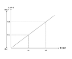
- FIG. 4 is a graph illustrating an example of a relationship between the output average and the standard deviation according to the first embodiment of the present technology.
- the vertical axis in the figure shows the average value of the signal level as the output average.
- the horizontal axis in the figure indicates the standard deviation.
- the standard deviation increases as the output average increases (that is, the ambient light becomes brighter). For example, when the output average AVb is larger than the output average AVa, the standard deviation ub corresponding to the output average AVb is larger than the standard deviation ua corresponding to the output average AVa.
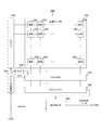
- FIG. 5 is a circuit diagram illustrating a configuration example of the pixel 230 according to the first embodiment of the present technology.
- the pixel 230 includes a photoelectric conversion element 231, a transfer transistor 232, a floating diffusion layer 233, an amplification transistor 234 and a selection transistor 235.
- the photoelectric conversion element 231 generates charges by photoelectrically converting incident light.
- the transfer transistor 232 transfers electric charge from the photoelectric conversion element 231 to the floating diffusion layer 233 in accordance with the transfer signal TRGm.
- m is an integer and indicates a row driven by the driver 210.
- the floating diffusion layer 233 generates a voltage corresponding to the amount of accumulated charges by accumulating charges.
- the amplifying transistor 234 generates an analog pixel signal by amplifying the voltage of the floating diffusion layer 233.
- the selection transistor 235 outputs a pixel signal to the column ADC 270 in accordance with the selection signal SELm.
- Driver 210 transmits a selection signal SELm to the selected row. In addition, the driver 210 transmits a transfer signal TRGm to the selected row at the start of exposure or at the end of exposure.
- a reset transistor is further required to initialize the floating diffusion layer 233. This is because it is necessary to read the reset level when performing the CDS process.
- the CDS process is not executed in the subsequent circuit, so that a reset transistor is not necessary, and the pixel circuit can be made relatively simple.
- FIG. 6 is a block diagram illustrating a configuration example of the column ADC 270 according to the first embodiment of the present technology.
- the column ADC 270 includes an AD converter 271 for each column.
- the AD converter 271 performs AD conversion on the pixel signal from the corresponding column to generate pixel data.
- the AD converter 271 compares the sawtooth ramp signal with the pixel signal and counts the count value until the comparison result is inverted. Then, the AD converter 271 supplies the count value data to the line buffer 280 as pixel data.
- the conversion gain of the AD converter 271 is fixed to a value (for example, 1LSB / e ⁇ ) that does not overflow the charge even when the light amount is the largest.
- the conversion gain indicates the ratio between the LSB (Least Significant Bit) and the charge amount. For example, if the shortest exposure time is 1/8000 second, if 1LSB / e ⁇ , the charge amount is 1024e ⁇ even when exposure is performed with the shortest exposure time, and it is considered that there is no saturation.
- the AD converter 271 is an example of an analog-digital converter described in the claims.
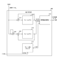
- FIG. 7 is a block diagram illustrating a configuration example of the statistical processing unit 300 according to the first embodiment of the present technology.
- the statistical processing unit 300 includes an adder 311, a frame memory 312, a standard deviation calculation unit 313, a multiplier 314, an adder 315, a frame memory 316, and a frame number counter 317.
- the frame memory 312 holds a sum SUM of pixel data x i (i is an integer from 1 to n) for each pixel. I subscript indicates that x i is the pixel data in the i-th frame among n frames.
- the adder 311 reads the sum SUM (1, 1) of the coordinates (1, 1) from the frame memory 312. , X i . Then, the adder 311 updates SUM (1, 1) in the frame memory 312 with the added value. In this way, the sum of pixel data at the same coordinates in each of the n frames is calculated.
- the adder 311 is an example of a sum adder described in the claims
- the frame memory 312 is an example of a sum holding unit described in the claims.
- the multiplier 314 calculates the square of the pixel data x i for each pixel.
- the multiplier 314 supplies the operation result x i 2 to the adder 315.
- the frame memory 316 holds the sum of squares SUMS of each pixel.
- the adder 315 reads the sum of squares SUMS of the pixel from the frame memory 312 and adds it to the x i 2 of the pixel. Then, the adder 315 holds the added data in the frame memory 316 as a new sum of squares SUMS.
- the adder 315 is an example of a square sum adder described in the claims
- the frame memory 316 is an example of a square sum holding unit described in the claims.
- the frame number counter 317 counts the number of generated image data. For example, the frame number counter 317 counts the count value i in synchronization with the vertical synchronization signal VSYNC and supplies it to the standard deviation calculation unit 313.
- the standard deviation calculation unit 313 pays attention to the pixels in order and calculates the standard deviation of the pixel data of the focused pixels.
- the standard deviation calculation unit 313 monitors the count value i, and starts calculating the standard deviation for all pixels when the count value i reaches a predetermined set number n. Further, the standard deviation calculation unit 313 supplies the reset signal RST to the frame number counter 317 to initialize the count value i.
- the set number n is set according to a user operation. For example, when imaging in a bright place, the user sets a large value for n, and when imaging in a dark place, a small value is set for n.
- the set number n may be set by the image capturing apparatus 100 by automatic exposure control instead of the user, as will be described later.
- the standard deviation u of x i is given by the following equation.
- x marked with bars represent the mean value of n x i. This average value is generally represented by the following equation.
- the standard deviation calculation unit 313 calculates the standard deviation u by substituting the sum SUM and square sum SUMS of the pixels and the set number n into Equation 3.
- the standard deviation u many information than x i obtained by one sampling, can be represented more gradations. For this reason, the dynamic range of the image data is expanded by using the standard deviation u as the signal value of the pixel.
- the standard deviation calculation unit 313 outputs data arranged in a two-dimensional grid using the standard deviation u of the pixel as a signal value to the DSP circuit 120 as HDR image data.
- the standard deviation calculation unit 313 can calculate the standard compilation from the sum SUM and the square sum SUMS without calculating the average value of the pixel data.
- the memory capacity can be reduced as compared with the case of using Equation 1.
- short-time imaging is additionally performed to obtain information on a brighter (larger light energy) light amount range.
- the light energy intensity in a wider range than before is expressed by compositing so as to compensate for a portion where information is lost due to saturation (overexposure) in normal exposure.
- the information can be enlarged in a brighter range, the feature is that the information is not enlarged so that the gradation can be obtained from the portion where the color is black (blackout).
- the imaging apparatus 100 that calculates the standard deviation, since the gradation expression is increased, for example, a gradation is generated even in a portion that is black (blackened), and a difference between light and dark can be obtained. . This suggests the possibility of capturing even the darkest part under the brightest subject imaging (exposure) conditions.
- the exposure times of the n frames are the same. For this reason, it is not necessary to greatly change the waveform of the ramp signal for each frame, and fine adjustment is sufficient. Further, since it is not necessary to greatly change the waveform of the ramp signal, it is not necessary to provide a circuit for changing the waveform. For this reason, the conversion gain is fixed to 1 LSB / e ⁇ which is an optimum value, for example.
- the statistical processing unit 300 calculates the standard deviation, but it can also calculate a statistic other than the standard deviation as long as it shows variation in pixel data. For example, the statistical processing unit 300 may calculate the variance instead of the standard deviation.
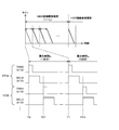
- FIG. 8 is a timing chart illustrating an example of the operation of the imaging apparatus 100 according to the first embodiment of the present technology. It is assumed that an operation (such as pressing a shutter button) for capturing an HDR image is performed at timing T0.
- the driver 210 in the imaging device 100 transmits the transfer signal TRG0 on the 0th row at the timing T0. In addition, the driver 210 transmits a high-level selection signal SEL0 over a certain period from the timing T0. By these controls, the pixels 230 in the 0th row are initialized, and the exposure in the 0th row is started.
- the driver 210 transmits the transfer signal TRG1 to the first row.
- the driver 210 transmits a high-level selection signal SEL1 over a certain period from the timing T01.
- the exposure for the first row is started.
- the second and subsequent exposures are sequentially started.
- the driver 210 transmits the transfer signal TRG0 in the 0th row at a timing T1 when a certain exposure time has elapsed from the timing T0. In addition, the driver 210 transmits a high-level selection signal SEL0 over a certain period from the timing T0. With these controls, the second exposure is started at the same time as the first exposure of the 0th row is completed.
- the driver 210 transmits the transfer signal TRG1 in the first row.
- the driver 210 transmits a high-level selection signal SEL1 over a certain period from the timing T11.
- the first exposure of the first row is completed and the second exposure is started at the same time.
- the second and subsequent exposures are sequentially started.
- the first image data is read out by exposing all rows.
- the second and subsequent image data are also read out by the same control.
- the exposure time of each image data is set to be the same (such as 1/16000 seconds).
- a sum SUM and a square sum SUMS are calculated for each pixel.
- the standard deviation u is calculated for each pixel, and the first HDR image data is generated. Similarly, the second and subsequent HDR image data are generated every time n image data are read out.
- the exposure time of one piece of image data is t 0
- the length of the HDR image capturing period for generating one piece of HDR image is n ⁇ t 0 .
- the exposure time t 0 per sheet is set to the minimum possible value (such as 1/16000 seconds). Since the exposure time t 0 is very short, the capacity of the floating diffusion layer 233 for storing charge may be relatively small, less influence of leakage of the charge. In addition, rolling shutter distortion hardly occurs because reading is performed at a very high speed.
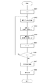
- FIG. 9 is a flowchart illustrating an example of the operation of the imaging apparatus 100 according to the first embodiment of the present technology. This operation is started, for example, when an operation for capturing an HDR image is performed.
- the imaging apparatus 100 initializes the variable i to “0” (step S901).
- the imaging apparatus 100 generates pixel data x i for each pixel (step S902), and adds the x i to the sum SUM (step S903). Further, the imaging apparatus 100 adds x i 2 to the sum of squares SUMS for each pixel (step S904).
- the imaging apparatus 100 increments the variable i (step S905), and determines whether the i is the set number n (step S906).
- step S906 When the variable i has not reached the set number n (step S906: No), the imaging apparatus 100 repeatedly executes step S902 and subsequent steps.
- step S906: Yes when the variable i is the set number n (step S906: Yes), the imaging apparatus 100 calculates the standard deviation u for each pixel to generate HDR image data (step S907). Then, the imaging apparatus 100 performs signal processing on the HDR image data (step S908), and ends the operation for capturing the HDR image.
- step S908 the imaging apparatus 100 repeatedly executes step S901 and subsequent steps.
- the imaging apparatus 100 obtains the standard deviation that does not change even if there is a DC component added to the signal value for each pixel. It is possible to improve the speed of signal processing without performing CDS processing or the like for reducing. In addition, in an imaging apparatus that captures image data, it is possible to acquire image information of gradation expressive power (that is, dynamic range) that exceeds the bit resolution of the mounted A / D converter.
- gradation expressive power that is, dynamic range
- the user sets the number of frames necessary for one HDR image (set number n). However, if the user makes an operation error, an inappropriate value is n. Therefore, the image quality of the HDR image data may be deteriorated. If the imaging apparatus 100 itself is configured to set the set number n by automatic exposure control, the image quality of the HDR image data can be improved by an appropriate value n.
- the imaging apparatus 100 according to the modification of the first embodiment is different from the first embodiment in that the set number n is set by automatic exposure control.
- FIG. 10 is a block diagram illustrating a configuration example of the solid-state imaging device 200 according to the modification of the first embodiment of the present technology.
- the solid-state imaging device 200 according to the modification of the first embodiment is different from the first embodiment in that it further includes a photometry unit 320 and an exposure control unit 330.
- the photometry unit 320 measures the brightness of the image data.
- the photometric unit 320 supplies an exposure value EV indicating the photometric amount to the exposure control unit 330.
- the exposure control unit 330 sets the set number n based on the exposure value EV.
- the exposure control unit 330 obtains the F value and ISO sensitivity of the imaging device 100, calculates the total exposure time t is the sum of n pieces of exposure time t 0 using the following equation.
- the unit of t is, for example, second (s).
- EV log 2 (F 2 / t) + log 2 (ISO / 100) Expression 4
- the exposure control unit 330 divides the total exposure time t by the exposure time t 0 per sheet (eg, 1/1600 seconds), and sets the divided quotient as n.
- the exposure control unit 330 supplies the set number n to the statistical processing unit 300.
- FIG. 11 is a diagram illustrating an example of a setting example of the set number n in the modification example of the first embodiment of the present technology.
- the imaging device 100 increases the total exposure time t and increases the set number n as the amount of ambient light decreases.
- the amount of light is “81920” lux (lx), and an exposure value EV of “15” is measured.
- F value is 5.6 and the ISO sensitivity is 400
- “1/4000” seconds (s) is calculated as the total exposure time t from Equation 4.
- the exposure time t 0 per sheet is “1/1600” seconds (s)
- the calculated “1/4000” seconds (s) is divided by the “1/1600” to obtain the set number n.
- “4” is calculated.
- the imaging apparatus 100 calculates the set number n from the light measurement amount, an appropriate set number n corresponding to the amount of ambient light is set. be able to.
- Second Embodiment> In the first embodiment described above, all the circuits (pixel array unit 220, etc.) in the solid-state imaging device 200 are arranged on one semiconductor substrate. However, in order to improve the resolution under a certain optical size (pixel array unit 220), it is necessary to make the pixels finer. This miniaturization increases the number of AD converters 271 and increases the circuit area other than the pixels, such as the area of the AD converter 271. That is, the area of the semiconductor substrate increases. Therefore, if the solid-state imaging device 200 is stacked on a plurality of semiconductor substrates, the pixel array unit 220 is disposed on one of the substrates, and the other is disposed on another substrate, the area of the semiconductor substrate can be reduced as compared with the case of not stacking. Can be small.
- the solid-state imaging device 200 according to the second embodiment is different from the first embodiment in that the solid-state imaging device 200 has a laminated structure in order to reduce the area of the semiconductor substrate.
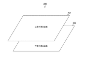
- FIG. 12 is an overall view showing a configuration example of the solid-state imaging device 200 according to the second embodiment.
- the fourth solid-state imaging device 200 includes a lower semiconductor substrate 202 and an upper semiconductor substrate 201 stacked on the substrate.
- FIG. 13 is a block diagram illustrating a configuration example of the solid-state imaging device 200 according to the second embodiment of the present technology.
- a driver 211 and a pixel array unit 220 are disposed on the upper semiconductor substrate 201. Further, on the lower semiconductor substrate 202, a timing control unit 250, a DAC 260, a circuit array unit 350, a memory reading unit 385, and a statistical processing unit 301 are arranged.
- a circuit block 360 is arranged for each pixel 230.
- the circuit block 360 performs AD conversion on the pixel signal of the corresponding pixel 230 to calculate the sum SUM and the square sum SUMS.
- the memory reading unit 385 reads the sum SUM and the square sum SUMS from each of the circuit blocks 360 and supplies it to the statistical processing unit 301.
- the driver 211 can drive the pixels 230 simultaneously. Note that the driver 211 may sequentially drive the pixels 230 for each row, as in the first embodiment. Note that although the circuit block 360 is provided for each pixel 230, the circuit block 360 may be provided for each region including a plurality of pixels 230.
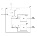
- FIG. 14 is a block diagram illustrating a configuration example of the circuit block 360 according to the second embodiment of the present technology.
- the circuit block 360 includes an AD converter 361, an adder 362, a memory 363, a multiplier 364, an adder 365, and a memory 366.
- the AD converter 361 performs AD conversion on the pixel signal of the corresponding pixel 230.
- the configurations of the adder 362, the memory 363, the multiplier 364, the adder 365, and the memory 366 are the same as those of the adder 311, the frame memory 312, the multiplier 314, the adder 315, and the frame memory 316 of the first embodiment. It is a configuration.
- FIG. 15 is a block diagram illustrating a configuration example of the statistical processing unit 301 according to the second embodiment of the present technology.
- the statistical processing unit 301 has the same configuration as the statistical processing unit 300 of the first embodiment, except that the frame memory 312, the multiplier 314, the adder 315, and the frame memory 316 are not provided.
- the circuits in the solid-state imaging device 200 are distributed and arranged on the two stacked semiconductor substrates, the area of the semiconductor substrate is smaller than in the case of not stacking. can do.
- the technology according to the present disclosure can be applied to various products.
- the technology according to the present disclosure may be any type of movement such as an automobile, an electric vehicle, a hybrid electric vehicle, a motorcycle, a bicycle, personal mobility, an airplane, a drone, a ship, a robot, a construction machine, and an agricultural machine (tractor). You may implement
- FIG. 16 is a block diagram illustrating a schematic configuration example of a vehicle control system 7000 that is an example of a mobile control system to which the technology according to the present disclosure can be applied.
- the vehicle control system 7000 includes a plurality of electronic control units connected via a communication network 7010.
- the vehicle control system 7000 includes a drive system control unit 7100, a body system control unit 7200, a battery control unit 7300, a vehicle exterior information detection unit 7400, a vehicle interior information detection unit 7500, and an integrated control unit 7600. .
- the communication network 7010 for connecting the plurality of control units conforms to an arbitrary standard such as CAN (Controller Area Network), LIN (Local Interconnect Network), LAN (Local Area Network), or FlexRay (registered trademark). It may be an in-vehicle communication network.
- Each control unit includes a microcomputer that performs arithmetic processing according to various programs, a storage unit that stores programs executed by the microcomputer or parameters used for various calculations, and a drive circuit that drives various devices to be controlled. Is provided.
- Each control unit includes a network I / F for communicating with other control units via a communication network 7010, and is connected to devices or sensors inside and outside the vehicle by wired communication or wireless communication. A communication I / F for performing communication is provided. In FIG.
- a microcomputer 7610 As a functional configuration of the integrated control unit 7600, a microcomputer 7610, a general-purpose communication I / F 7620, a dedicated communication I / F 7630, a positioning unit 7640, a beacon receiving unit 7650, an in-vehicle device I / F 7660, an audio image output unit 7670, An in-vehicle network I / F 7680 and a storage unit 7690 are illustrated.
- other control units include a microcomputer, a communication I / F, a storage unit, and the like.
- the drive system control unit 7100 controls the operation of the device related to the drive system of the vehicle according to various programs.
- the drive system control unit 7100 includes a driving force generator for generating a driving force of a vehicle such as an internal combustion engine or a driving motor, a driving force transmission mechanism for transmitting the driving force to wheels, and a steering angle of the vehicle. It functions as a control device such as a steering mechanism that adjusts and a braking device that generates a braking force of the vehicle.
- the drive system control unit 7100 may have a function as a control device such as ABS (Antilock Brake System) or ESC (Electronic Stability Control).
- a vehicle state detection unit 7110 is connected to the drive system control unit 7100.
- the vehicle state detection unit 7110 includes, for example, a gyro sensor that detects the angular velocity of the rotational movement of the vehicle body, an acceleration sensor that detects the acceleration of the vehicle, an operation amount of an accelerator pedal, an operation amount of a brake pedal, and steering of a steering wheel. At least one of sensors for detecting an angle, an engine speed, a rotational speed of a wheel, or the like is included.
- the drive system control unit 7100 performs arithmetic processing using a signal input from the vehicle state detection unit 7110, and controls an internal combustion engine, a drive motor, an electric power steering device, a brake device, or the like.
- the body system control unit 7200 controls the operation of various devices mounted on the vehicle body according to various programs.
- the body system control unit 7200 functions as a keyless entry system, a smart key system, a power window device, or a control device for various lamps such as a headlamp, a back lamp, a brake lamp, a blinker, or a fog lamp.
- the body control unit 7200 can be input with radio waves or various switch signals transmitted from a portable device that substitutes for a key.
- the body system control unit 7200 receives input of these radio waves or signals, and controls a door lock device, a power window device, a lamp, and the like of the vehicle.
- the battery control unit 7300 controls the secondary battery 7310 that is a power supply source of the drive motor according to various programs. For example, information such as battery temperature, battery output voltage, or remaining battery capacity is input to the battery control unit 7300 from a battery device including the secondary battery 7310. The battery control unit 7300 performs arithmetic processing using these signals, and controls the temperature adjustment of the secondary battery 7310 or the cooling device provided in the battery device.
- the outside information detection unit 7400 detects information outside the vehicle on which the vehicle control system 7000 is mounted.
- the outside information detection unit 7400 is connected to at least one of the imaging unit 7410 and the outside information detection unit 7420.
- the imaging unit 7410 includes at least one of a ToF (Time Of Flight) camera, a stereo camera, a monocular camera, an infrared camera, and other cameras.
- the outside information detection unit 7420 detects, for example, current weather or an environmental sensor for detecting weather, or other vehicles, obstacles, pedestrians, etc. around the vehicle equipped with the vehicle control system 7000. At least one of the surrounding information detection sensors.
- the environmental sensor may be, for example, at least one of a raindrop sensor that detects rainy weather, a fog sensor that detects fog, a sunshine sensor that detects sunlight intensity, and a snow sensor that detects snowfall.
- the ambient information detection sensor may be at least one of an ultrasonic sensor, a radar device, and a LIDAR (Light Detection and Ranging, Laser Imaging Detection and Ranging) device.
- the imaging unit 7410 and the outside information detection unit 7420 may be provided as independent sensors or devices, or may be provided as a device in which a plurality of sensors or devices are integrated.
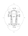
- FIG. 17 shows an example of installation positions of the imaging unit 7410 and the vehicle outside information detection unit 7420.
- the imaging units 7910, 7912, 7914, 7916, and 7918 are provided at, for example, at least one of the front nose, the side mirror, the rear bumper, the back door, and the upper part of the windshield in the vehicle interior of the vehicle 7900.
- An imaging unit 7910 provided in the front nose and an imaging unit 7918 provided in the upper part of the windshield in the vehicle interior mainly acquire an image in front of the vehicle 7900.
- Imaging units 7912 and 7914 provided in the side mirror mainly acquire an image of the side of the vehicle 7900.
- An imaging unit 7916 provided in the rear bumper or the back door mainly acquires an image behind the vehicle 7900.
- the imaging unit 7918 provided on the upper part of the windshield in the passenger compartment is mainly used for detecting a preceding vehicle or a pedestrian, an obstacle, a traffic light, a traffic sign, a lane, or
- FIG. 17 shows an example of shooting ranges of the respective imaging units 7910, 7912, 7914, and 7916.
- the imaging range a indicates the imaging range of the imaging unit 7910 provided in the front nose
- the imaging ranges b and c indicate the imaging ranges of the imaging units 7912 and 7914 provided in the side mirrors, respectively
- the imaging range d The imaging range of the imaging part 7916 provided in the rear bumper or the back door is shown. For example, by superimposing the image data captured by the imaging units 7910, 7912, 7914, and 7916, an overhead image when the vehicle 7900 is viewed from above is obtained.
- the vehicle outside information detection units 7920, 7922, 7924, 7926, 7928, and 7930 provided on the front, rear, sides, corners of the vehicle 7900 and the upper part of the windshield in the vehicle interior may be, for example, an ultrasonic sensor or a radar device.
- the vehicle outside information detection units 7920, 7926, and 7930 provided on the front nose, the rear bumper, the back door, and the windshield in the vehicle interior of the vehicle 7900 may be, for example, LIDAR devices.
- These outside information detection units 7920 to 7930 are mainly used for detecting a preceding vehicle, a pedestrian, an obstacle, and the like.
- the vehicle exterior information detection unit 7400 causes the imaging unit 7410 to capture an image outside the vehicle and receives the captured image data. Further, the vehicle exterior information detection unit 7400 receives detection information from the vehicle exterior information detection unit 7420 connected thereto.
- the vehicle exterior information detection unit 7420 is an ultrasonic sensor, a radar device, or a LIDAR device
- the vehicle exterior information detection unit 7400 transmits ultrasonic waves, electromagnetic waves, or the like, and receives received reflected wave information.
- the outside information detection unit 7400 may perform an object detection process or a distance detection process such as a person, a car, an obstacle, a sign, or a character on a road surface based on the received information.
- the vehicle exterior information detection unit 7400 may perform environment recognition processing for recognizing rainfall, fog, road surface conditions, or the like based on the received information.
- the vehicle outside information detection unit 7400 may calculate a distance to an object outside the vehicle based on the received information.
- the outside information detection unit 7400 may perform image recognition processing or distance detection processing for recognizing a person, a car, an obstacle, a sign, a character on a road surface, or the like based on the received image data.
- the vehicle exterior information detection unit 7400 performs processing such as distortion correction or alignment on the received image data, and combines the image data captured by the different imaging units 7410 to generate an overhead image or a panoramic image. Also good.
- the vehicle exterior information detection unit 7400 may perform viewpoint conversion processing using image data captured by different imaging units 7410.
- the vehicle interior information detection unit 7500 detects vehicle interior information.
- a driver state detection unit 7510 that detects the driver's state is connected to the in-vehicle information detection unit 7500.
- Driver state detection unit 7510 may include a camera that captures an image of the driver, a biosensor that detects biometric information of the driver, a microphone that collects sound in the passenger compartment, and the like.
- the biometric sensor is provided, for example, on a seat surface or a steering wheel, and detects biometric information of an occupant sitting on the seat or a driver holding the steering wheel.
- the vehicle interior information detection unit 7500 may calculate the degree of fatigue or concentration of the driver based on the detection information input from the driver state detection unit 7510, and determines whether the driver is asleep. May be.
- the vehicle interior information detection unit 7500 may perform a process such as a noise canceling process on the collected audio signal.
- the integrated control unit 7600 controls the overall operation in the vehicle control system 7000 according to various programs.
- An input unit 7800 is connected to the integrated control unit 7600.
- the input unit 7800 is realized by a device that can be input by a passenger, such as a touch panel, a button, a microphone, a switch, or a lever.
- the integrated control unit 7600 may be input with data obtained by recognizing voice input through a microphone.
- the input unit 7800 may be, for example, a remote control device using infrared rays or other radio waves, or may be an external connection device such as a mobile phone or a PDA (Personal Digital Assistant) that supports the operation of the vehicle control system 7000. May be.
- the input unit 7800 may be, for example, a camera.
- the passenger can input information using a gesture.
- data obtained by detecting the movement of the wearable device worn by the passenger may be input.
- the input unit 7800 may include, for example, an input control circuit that generates an input signal based on information input by a passenger or the like using the input unit 7800 and outputs the input signal to the integrated control unit 7600.
- a passenger or the like operates the input unit 7800 to input various data or instruct a processing operation to the vehicle control system 7000.
- the storage unit 7690 may include a ROM (Read Only Memory) that stores various programs executed by the microcomputer, and a RAM (Random Access Memory) that stores various parameters, calculation results, sensor values, and the like.
- the storage unit 7690 may be realized by a magnetic storage device such as an HDD (Hard Disc Drive), a semiconductor storage device, an optical storage device, a magneto-optical storage device, or the like.
- General-purpose communication I / F 7620 is a general-purpose communication I / F that mediates communication with various devices existing in the external environment 7750.
- General-purpose communication I / F7620 is a cellular communication protocol such as GSM (Global System of Mobile communications), WiMAX, LTE (Long Term Evolution) or LTE-A (LTE-Advanced), or wireless LAN (Wi-Fi (registered trademark)). Other wireless communication protocols such as Bluetooth (registered trademark) may also be implemented.
- the general-purpose communication I / F 7620 is connected to a device (for example, an application server or a control server) existing on an external network (for example, the Internet, a cloud network, or an operator-specific network) via, for example, a base station or an access point.
- the general-purpose communication I / F 7620 is a terminal (for example, a driver, a pedestrian or a store terminal, or an MTC (Machine Type Communication) terminal) that exists in the vicinity of the vehicle using, for example, P2P (Peer To Peer) technology. You may connect with.
- a terminal for example, a driver, a pedestrian or a store terminal, or an MTC (Machine Type Communication) terminal
- P2P Peer To Peer
- the dedicated communication I / F 7630 is a communication I / F that supports a communication protocol formulated for use in vehicles.
- the dedicated communication I / F 7630 is a standard protocol such as WAVE (Wireless Access in Vehicle Environment), DSRC (Dedicated Short Range Communications), or cellular communication protocol, which is a combination of the lower layer IEEE 802.11p and the upper layer IEEE 1609. May be implemented.
- the dedicated communication I / F 7630 typically includes vehicle-to-vehicle communication, vehicle-to-infrastructure communication, vehicle-to-home communication, and vehicle-to-pedestrian communication. ) Perform V2X communication, which is a concept that includes one or more of the communications.
- the positioning unit 7640 receives, for example, a GNSS signal from a GNSS (Global Navigation Satellite System) satellite (for example, a GPS signal from a GPS (Global Positioning System) satellite), performs positioning, and performs latitude, longitude, and altitude of the vehicle.
- the position information including is generated.
- the positioning unit 7640 may specify the current position by exchanging signals with the wireless access point, or may acquire position information from a terminal such as a mobile phone, PHS, or smartphone having a positioning function.
- the beacon receiving unit 7650 receives, for example, radio waves or electromagnetic waves transmitted from a radio station installed on the road, and acquires information such as the current position, traffic jam, closed road, or required time. Note that the function of the beacon receiving unit 7650 may be included in the dedicated communication I / F 7630 described above.
- the in-vehicle device I / F 7660 is a communication interface that mediates the connection between the microcomputer 7610 and various in-vehicle devices 7760 present in the vehicle.
- the in-vehicle device I / F 7660 may establish a wireless connection using a wireless communication protocol such as a wireless LAN, Bluetooth (registered trademark), NFC (Near Field Communication), or WUSB (Wireless USB).
- the in-vehicle device I / F 7660 is connected to a USB (Universal Serial Bus), HDMI (High-Definition Multimedia Interface), or MHL (Mobile High-definition Link) via a connection terminal (and a cable if necessary). ) Etc. may be established.
- the in-vehicle device 7760 may include, for example, at least one of a mobile device or a wearable device that a passenger has, or an information device that is carried into or attached to the vehicle.
- In-vehicle device 7760 may include a navigation device that searches for a route to an arbitrary destination.
- In-vehicle device I / F 7660 exchanges control signals or data signals with these in-vehicle devices 7760.
- the in-vehicle network I / F 7680 is an interface that mediates communication between the microcomputer 7610 and the communication network 7010.
- the in-vehicle network I / F 7680 transmits and receives signals and the like in accordance with a predetermined protocol supported by the communication network 7010.
- the microcomputer 7610 of the integrated control unit 7600 is connected via at least one of a general-purpose communication I / F 7620, a dedicated communication I / F 7630, a positioning unit 7640, a beacon receiving unit 7650, an in-vehicle device I / F 7660, and an in-vehicle network I / F 7680.
- the vehicle control system 7000 is controlled according to various programs based on the acquired information. For example, the microcomputer 7610 calculates a control target value of the driving force generation device, the steering mechanism, or the braking device based on the acquired information inside and outside the vehicle, and outputs a control command to the drive system control unit 7100. Also good.
- the microcomputer 7610 realizes ADAS (Advanced Driver Assistance System) functions including vehicle collision avoidance or impact mitigation, following traveling based on inter-vehicle distance, vehicle speed maintaining traveling, vehicle collision warning, or vehicle lane departure warning. You may perform the cooperative control for the purpose. Further, the microcomputer 7610 controls the driving force generator, the steering mechanism, the braking device, or the like based on the acquired information on the surroundings of the vehicle, so that the microcomputer 7610 automatically travels independently of the driver's operation. You may perform the cooperative control for the purpose of driving.
- ADAS Advanced Driver Assistance System
- the microcomputer 7610 is information acquired via at least one of the general-purpose communication I / F 7620, the dedicated communication I / F 7630, the positioning unit 7640, the beacon receiving unit 7650, the in-vehicle device I / F 7660, and the in-vehicle network I / F 7680.
- the three-dimensional distance information between the vehicle and the surrounding structure or an object such as a person may be generated based on the above and local map information including the peripheral information of the current position of the vehicle may be created.
- the microcomputer 7610 may generate a warning signal by predicting a danger such as a collision of a vehicle, approach of a pedestrian or the like or an approach to a closed road based on the acquired information.
- the warning signal may be, for example, a signal for generating a warning sound or lighting a warning lamp.
- the audio image output unit 7670 transmits an output signal of at least one of audio and image to an output device capable of visually or audibly notifying information to a vehicle occupant or the outside of the vehicle.
- an audio speaker 7710, a display unit 7720, and an instrument panel 7730 are illustrated as output devices.
- Display unit 7720 may include at least one of an on-board display and a head-up display, for example.
- the display portion 7720 may have an AR (Augmented Reality) display function.
- the output device may be other devices such as headphones, wearable devices such as glasses-type displays worn by passengers, projectors, and lamps.
- the display device can display the results obtained by various processes performed by the microcomputer 7610 or information received from other control units in various formats such as text, images, tables, and graphs. Display visually. Further, when the output device is an audio output device, the audio output device converts an audio signal made up of reproduced audio data or acoustic data into an analog signal and outputs it aurally.
- At least two control units connected via the communication network 7010 may be integrated as one control unit.
- each control unit may be configured by a plurality of control units.
- the vehicle control system 7000 may include another control unit not shown.
- some or all of the functions of any of the control units may be given to other control units. That is, as long as information is transmitted and received via the communication network 7010, the predetermined arithmetic processing may be performed by any one of the control units.
- a sensor or device connected to one of the control units may be connected to another control unit, and a plurality of control units may transmit / receive detection information to / from each other via the communication network 7010. .
- the solid-state imaging device 200 can be applied to the integrated control unit 7600 of the application example illustrated in FIG.
- the solid-state imaging device 200 corresponds to the imaging unit 7410 of the integrated control unit 7600.
- the integrated control unit 7600 calculates the standard deviation for each pixel, so that the dynamic range can be expanded and the signal processing speed can be improved.
- At least a part of the components of the solid-state imaging device 200 described with reference to FIG. 2 is realized in a module (for example, an integrated circuit module including one die) for the integrated control unit 7600 illustrated in FIG. May be. Or the solid-state image sensor 200 demonstrated using FIG. 2 may be implement
- the processing procedure described in the above embodiment may be regarded as a method having a series of these procedures, and a program for causing a computer to execute these series of procedures or a recording medium storing the program. You may catch it.
- a recording medium for example, a CD (Compact Disc), an MD (MiniDisc), a DVD (Digital Versatile Disc), a memory card, a Blu-ray disc (Blu-ray (registered trademark) Disc), or the like can be used.
- this technique can also take the following structures.
- a pixel array unit in which a plurality of pixels each generating a pixel signal are arranged in a two-dimensional lattice;
- a solid-state imaging device comprising: a statistical processing unit that acquires a statistic indicating a degree of variation of the pixel signal of each of the plurality of pixels as a signal value of each of the plurality of pixels.
- the solid-state imaging device according to (1) further including a driver that drives the pixel array unit to generate an image signal including the pixel signal a plurality of times.
- the statistical processing unit acquires a standard deviation of the pixel signal as the statistical quantity.
- the statistical processing unit A sum total holding unit that holds the sum of the pixel signals for each of the plurality of pixels; A sum adder that calculates the sum for each of the plurality of pixels and holds the sum in the sum retaining unit; A sum of squares holding unit that holds the sum of squares of the pixel signals for each of the plurality of pixels; A multiplier for calculating a square of the pixel signal for each of the plurality of pixels; A square sum adder that calculates the sum of squares for each of the plurality of pixels and holds the sum of squares in the square sum holding unit;
- the solid-state imaging device according to (2), further comprising: an arithmetic unit that calculates the statistic from the sum, the square sum, and the number of the generated image signals.
- the statistical processing unit counts the number of generated image signals, and calculates the statistical amount from the sum and square sum of the pixel signals and the set number when the count value is a predetermined set number.
- the solid-state imaging device according to any one of (2) to (5), wherein: (7)
- the pixel array unit and the driver are arranged on a predetermined semiconductor substrate, The solid-state imaging device according to any one of (1) to (7), wherein the statistical processing unit is disposed on a semiconductor substrate stacked on the predetermined semiconductor substrate. (9) The solid-state imaging device according to any one of (1) to (8), further including an analog-digital conversion unit that performs analog-digital conversion on the pixel signal. (10) The solid-state imaging device according to (9), wherein the analog-digital conversion unit includes an analog-digital converter for each of the plurality of pixels. (11) The solid-state imaging device according to (9), wherein the analog-to-digital conversion unit includes an analog-to-digital converter for each of lines formed of pixels arranged in a predetermined direction.
- Each of the plurality of pixels is A photoelectric conversion element that photoelectrically converts light to generate charges; A floating diffusion layer for accumulating the charge; A transfer transistor for transferring the charge from the photoelectric conversion element to the floating diffusion layer according to a transfer signal; An amplification transistor that amplifies the voltage of the floating diffusion layer and outputs a pixel signal;
- the solid-state imaging device according to any one of (1) to (11), further including a selection transistor that outputs the pixel signal to the analog-digital converter according to a selection signal.
- a pixel array unit in which a plurality of pixels each generating a pixel signal are arranged in a two-dimensional lattice;
- a statistical processing unit that acquires a statistic indicating a degree of variation of the pixel signal of each of the plurality of pixels as a signal value of each of the plurality of pixels;
- a signal processing apparatus comprising: a signal processing unit that performs predetermined signal processing on the image data including the signal values.
- a generation procedure in which each of a plurality of pixels generates a pixel signal comprising: a statistical processing procedure that acquires a statistic indicating a degree of variation of the pixel signal of each of the plurality of pixels as a signal value of each of the plurality of pixels.
- Imaging device 110 Imaging lens 120 DSP circuit 130 Imaging control part 140 Recording part 200 Solid-state image sensor 201 Upper semiconductor substrate 202 Lower semiconductor substrate 210, 211 Driver 220 Pixel array part 230 Pixel 231 Photoelectric conversion element 232 Transfer transistor 233 Floating diffusion layer 234 Amplification transistor 235 Selection transistor 250 Timing control unit 260 DAC 270 column ADC 271, 361 AD converter 280 Line buffer 300, 301 Statistical processing unit 311, 315, 362, 365 Adder 312, 316 Frame memory 313 Standard deviation calculation unit 314, 364 Multiplier 317 Frame number counter 320 Photometry unit 330 Exposure control unit 350 Circuit array unit 360 Circuit block 363, 366 Memory 385 Memory reading unit 7410 Imaging unit
Landscapes
- Engineering & Computer Science (AREA)
- Multimedia (AREA)
- Signal Processing (AREA)
- Transforming Light Signals Into Electric Signals (AREA)
Abstract
画像データを撮像する撮像装置において、搭載しているA/D変換器のビット解像度を超える階調表現力(すなわち、ダイナミックレンジ)の画像情報を取得する。 固体撮像素子は、画素アレイ部と、統計処理部とを具備する。この固体撮像素子において画素アレイ部には、それぞれが画素信号を生成する複数の画素が二次元格子状に配列される。また、この固体撮像素子において、統計処理部は、画素アレイ部内の複数の画素それぞれの画素信号のばらつきの度合いを示す統計量を複数の画素それぞれの信号値として取得する。
Description
本技術は、固体撮像素子、信号処理装置、および、固体撮像素子の制御方法に関する。詳しくは、複数の画像データを撮像する固体撮像素子、信号処理装置、および、固体撮像素子の制御方法に関する。
従来より、撮像装置においては、通常より広いダイナミックレンジを実現するために、HDR(High Dynamic Range)合成と呼ばれる画像合成技術が用いられている。例えば、露光時間の異なる複数の画像を撮像し、それらの画像をHDR合成する撮像装置が提案されている(例えば、特許文献1参照。)。
上述のような従来技術では、複数枚の露出時間の異なる画像データを部分選択的に合成したり、演算合成したりして情報量を増加させているが、それによって得られる情報量の増加は、最大でも画像枚数とA/D(Analog to Digital)変換器の解像度の積までである。例えば10bit(1024階調)の画像データ2枚から得られる合成した情報量は異なる露光時間の撮像によって表現できる光エネルギーの範囲を広げる事はできるが、2048階調の情報以上にはなりえない。これは、別条件で撮像した別画像の情報を追加しているという事であり、元々の情報をより細かい精度で測定して情報解像度を向上させているわけでは無かった。さらに、従来の方法では、複数露光画像の同時性(同時刻性)や保存するフレームメモリのコストやサイズの制約もあり、より多くの情報を増やすために枚数を無制限に増加させる事は困難であった。一方、直接的にA/D変換器の解像度を上げる事は処理時間の増加と回路コストの増加から容易ではないとされてきた。
本技術はこのような状況に鑑みて生み出されたものであり、画像データを撮像する撮像装置において、搭載しているA/D変換器のビット解像度を超える階調表現力(すなわち、ダイナミックレンジ)の画像情報を取得することを目的とする。
本技術は、上述の問題点を解消するためになされたものであり、その第1の側面は、それぞれが画素信号を生成する複数の画素が二次元格子状に配列された画素アレイ部と、上記複数の画素それぞれの上記画素信号のばらつきの度合いを示す統計量を上記複数の画素それぞれの信号値として取得する統計処理部とを具備する固体撮像素子、および、その制御方法である。これにより、画素信号のばらつきの度合いを示す統計量が信号値として取得されるという作用をもたらす。
また、この第1の側面において、上記画素アレイ部を駆動して上記画素信号からなる画像信号を生成させる制御を複数回に亘って行うドライバをさらに具備してもよい。これにより、複数の画像信号が生成されるという作用をもたらす。
また、この第1の側面において、上記統計処理部は、上記画素信号の標準偏差を上記統計量として取得してもよい。これにより、標準偏差が取得されるという作用をもたらす。
また、この第1の側面において、上記統計処理部は、上記複数の画素のそれぞれについて上記画素信号の総和を保持する総和保持部と、上記複数の画素のそれぞれについて上記総和を演算して上記総和保持部に保持させる総和加算器と、上記複数の画素のそれぞれについて上記画素信号の二乗和を保持する二乗和保持部と、上記複数の画素のそれぞれについて上記画素信号の二乗を演算する乗算器と、上記複数の画素のそれぞれについて上記二乗の和を演算して上記二乗和として上記二乗和保持部に保持させる二乗和加算器と、上記総和と上記二乗和と上記生成された画像信号の枚数とから上記統計量を演算する演算部とを備えてもよい。これにより、総和と二乗和と生成された画像信号の枚数とから統計量が演算されるという作用をもたらす。
また、この第1の側面において、上記複数の画素のそれぞれについて上記画素信号の総和および二乗和を演算する回路ブロックをさらに具備し、上記統計処理部は、上記総和と上記二乗和と上記生成された画像信号の枚数とから上記統計量を演算してもよい。これにより、回路ブロックからの総和と二乗和と生成された画像信号の枚数とから統計量が演算されるという作用をもたらす。
また、この第1の側面において、上記統計処理部は、上記画像信号が生成された枚数を計数して当該計数値が所定の設定枚数であるときの上記画素信号の総和および二乗和と上記設定枚数とから上記統計量を演算してもよい。これにより、計数値が所定の設定枚数であるときの画素信号の総和および二乗和と設定枚数とから統計量が演算されるという作用をもたらす。
また、この第1の側面において、測光量に基づいて上記設定枚数を演算する露光制御部をさらに具備してもよい。これにより、測光量に基づいて設定枚数が演算されるという作用をもたらす。
また、この第1の側面において、上記画素アレイ部および上記ドライバは、所定の半導体基板に配置され、上記統計処理部は、上記所定の半導体基板に積層された半導体基板に配置されてもよい。これにより、積層構造の固体撮像素子において統計量が取得されるという作用をもたらす。
また、この第1の側面において、上記画素信号に対してアナログデジタル変換を行うアナログデジタル変換部をさらに具備してもよい。これにより、画素信号に対してアナログデジタル変換が行われるという作用をもたらす。
また、この第1の側面において、上記アナログデジタル変換部は、上記複数の画素のそれぞれについてアナログデジタル変換器を備えてもよい。これにより、画素ごとのアナログデジタル変換器によってアナログデジタル変換が行われるという作用をもたらす。
また、この第1の側面において、上記アナログデジタル変換部は、所定の方向に配列された画素からなるラインのそれぞれについてアナログデジタル変換器を備えてもよい。これにより、ラインごとのアナログデジタル変換器によってアナログデジタル変換が行われるという作用をもたらす。
また、この第1の側面において、上記複数の画素のそれぞれは、光を光電変換して電荷を生成する光電変換素子と、上記電荷を蓄積する浮遊拡散層と、転送信号に従って上記光電変換素子から上記浮遊拡散層へ上記電荷を転送する転送トランジスタと、上記浮遊拡散層の電圧を増幅して画素信号を出力する増幅トランジスタと、選択信号に従って上記画素信号を上記アナログデジタル変換器に出力する選択トランジスタとを備えてもよい。これにより、リセットトランジスタが設けられない画素により画素信号が生成されるという作用をもたらす。
また、本技術の第2の側面は、それぞれが画素信号を生成する複数の画素が二次元格子状に配列された画素アレイ部と、上記複数の画素それぞれの上記画素信号のばらつきの度合いを示す統計量を上記複数の画素それぞれの信号値として取得する統計処理部と、上記信号値からなる画像データに対して所定の信号処理を実行する信号処理部とを具備する信号処理装置である。これにより、画素信号のばらつきの度合いを示す統計量が信号値として取得され、その信号値からなる画像データに対して所定の信号処理が実行されるという作用をもたらす。
本技術によれば、画像データを撮像する撮像装置において、搭載しているA/D変換器のビット解像度を超える階調表現力(すなわち、ダイナミックレンジ)の画像情報を取得することができるという優れた効果を奏し得る。なお、ここに記載された効果は必ずしも限定されるものではなく、本開示中に記載されたいずれかの効果であってもよい。
以下、本技術を実施するための形態(以下、実施の形態と称する)について説明する。説明は以下の順序により行う。
1.第1の実施の形態(画素毎に標準偏差を演算する例)
2.第2の実施の形態(積層構造の固体撮像素子において画素毎に標準偏差を演算する例)
1.第1の実施の形態(画素毎に標準偏差を演算する例)
2.第2の実施の形態(積層構造の固体撮像素子において画素毎に標準偏差を演算する例)
<1.第1の実施の形態>
[撮像装置の構成例]
図1は、本技術の第1の実施の形態における撮像装置100の一構成例を示すブロック図である。この撮像装置100は、画像データ(フレーム)を撮像するものであり、撮像レンズ110、固体撮像素子200、DSP(Digital Signal Processing)回路120、撮像制御部130および記録部140を備える。なお、撮像装置100は、特許請求の範囲に記載の信号処理装置の一例である。
[撮像装置の構成例]
図1は、本技術の第1の実施の形態における撮像装置100の一構成例を示すブロック図である。この撮像装置100は、画像データ(フレーム)を撮像するものであり、撮像レンズ110、固体撮像素子200、DSP(Digital Signal Processing)回路120、撮像制御部130および記録部140を備える。なお、撮像装置100は、特許請求の範囲に記載の信号処理装置の一例である。
撮像レンズ110は、光を集光して固体撮像素子200に導くものである。固体撮像素子200は、入射光を光電変換してフレームを撮像するものである。固体撮像素子200として、例えば、CMOS(Complementary MOS)イメージセンサーが用いられる。この固体撮像素子200は、ダイナミックレンジを拡張したHDR画像データを複数のフレームから生成する。そして、固体撮像素子200は、生成したHDR画像データをDSP回路120に信号線209を介して供給する。なお、CMOSイメージセンサーの代わりに、CCD(Charge Coupled Device)イメージセンサーを用いてもよい。
DSP回路120は、HDR画像データに対して所定の信号処理を実行するものである。信号処理として、画素データのデータサイズを調整する処理や画素データを正規化する処理が実行される。この他、ホワイトバランス処理やデモザイク処理なども実行される。DSP回路120は、信号処理後のHDR画像データを記録部140に記憶させる。なお、DSP回路120は、特許請求の範囲に記載の信号処理部の一例である。
撮像制御部130は、固体撮像素子200を制御してフレームを撮像させるものである。この撮像制御部130は、露光時間を設定するための情報や垂直同期信号VSYNCなどを含む制御信号を固体撮像素子200に信号線139を介して供給する。この垂直同期信号VSYNCは、フレームを撮像するタイミングを示す同期信号である。
ここで、固体撮像素子200およびDSP回路120において、CDS処理およびダーク補正の両方は、いずれも不要であるため実行されない。これらを実行する必要がない理由については後述する。
[固体撮像素子の構成例]
図2は、本技術の第1の実施の形態における固体撮像素子200の一構成例を示すブロック図である。この固体撮像素子200は、ドライバ210、画素アレイ部220、タイミング制御部250、DAC(Digital to Analog Converter)260、カラムADC270、ラインバッファ280および統計処理部300を備える。これらの回路は、同一の半導体基板に配置される。
図2は、本技術の第1の実施の形態における固体撮像素子200の一構成例を示すブロック図である。この固体撮像素子200は、ドライバ210、画素アレイ部220、タイミング制御部250、DAC(Digital to Analog Converter)260、カラムADC270、ラインバッファ280および統計処理部300を備える。これらの回路は、同一の半導体基板に配置される。
画素アレイ部220には、複数の画素230が二次元格子状に配列される。これらの画素230は、光を光電変換してアナログの画素信号を生成するものである。
以下、所定の方向(水平方向など)に配列された画素230の集合を「行」と称し、行に垂直な方向に配列された画素230の集合を「列」と称する。
ドライバ210は、行を順に駆動して画素信号を出力させるものである。DAC260は、デジタルアナログ変換により、のこぎり刃状のランプ信号を生成するものである。このDAC260は、生成したランプ信号をカラムADC270に供給する。
カラムADC270は、行ごとに、その行内の画素230の画素信号をAD変換して画素データを生成するものである。このカラムADC270は、画素データのそれぞれをラインバッファ280に供給する。なお、カラムADC270は、特許請求の範囲に記載のアナログデジタル変換部の一例である。
タイミング制御部250は、垂直同期信号VSYNCに同期して、ドライバ210およびカラムADC270のそれぞれの動作タイミングを制御するものである。また、タイミング制御部250は、DAC260を制御してランプ信号を生成させる。
ラインバッファ280は、行内の画素230のそれぞれの画素データを保持するものである。ラインバッファ280は、保持した画素データを統計処理部300に順に供給する。
統計処理部300は、画素に順に着目して、その着目した画素の画素データのばらつきを示す統計量を演算するものである。例えば、統計量として標準偏差が演算される。この統計処理部300は、演算した標準偏差を信号値として、それらの信号値を二次元格子状に配列したデータをHDR画像データとしてDSP回路120に供給する。
なお、統計処理部300を固体撮像素子200内部に配置しているが、統計処理部300を固体撮像素子200の外部(DSP回路120など)に配置してもよい。
図3は、本技術の第1の実施の形態における信号レベルの分布の一例を示すグラフである。同図における横軸は、ある着目画素の信号レベルを示す。また、縦軸は、その着目画素について、信号レベルをサンプリングした回数であるサンプル数を示す。また、細い実線の曲線は、輝度が比較的低い環境下でサンプリングした信号レベルの分布の一例を示し、太い実線の曲線は、輝度が比較的高い環境下でサンプリングした信号レベルの分布の一例を示す。
これらの信号レベルの分布の標準偏差は、光雑音の影響を受けて、環境光の輝度が高くなるほど大きくなる。例えば、輝度が高いときの標準偏差ubは、輝度が低いときの標準偏差uaよりも大きい。光雑音は、光子数に依存するため、その光雑音により変動する標準偏差を、画素の受光量を示す信号値として扱うことができる。
ここで、AD変換されたデジタル信号の値が不正確となる原因としては、「0」基点がずれる場合と信号の読み取りがずれる場合との二通りが考えられる。前述のCDS処理やダーク補正は「0」基点をより正確にするための調整である。「0」基点がずれる理由は、回路の直流成分(電圧変動)や暗電流ノイズにより電圧が浮き上がる現象が生じるためである。「0」基点のずれによる影響を軽減するために、標準偏差を演算しない一般的な固体撮像素子においては、CDS補正やダーク補正が必要とされる。
一方、標準偏差は、変動量であるため、その元となるデータが正確に「0」基準からの絶対値である必要がなく、例えば、信号値に一律一定値が付加されるような直流成分があっても、変動量(変動幅)は変わらない。したがって、直流成分があっても標準偏差の計算には影響がない。このように「0」基準の正確性が求められないので、固体撮像素子200では、CDS補正やダーク補正が必要なく、そのためにかかっていた時間を節約することができる。
次に、信号の読み取りズレを低減するための方法として、AD変換後のデジタル信号のビット数を増大する方法が考えられる。ただし、AD変換器の分解能の向上によりビット数を増加させると、AD変換器内のコンパレータの比較回数が増加じて処理時間の増加につながるデメリットが生じてしまう。これに対して、固体撮像素子200では、AD変換器の分解能自体は変えずに、標準偏差計算に用いるサンプル数(フレーム数)の増加によって、最終的に得られるデジタル信号のビット数を増大している。したがって、AD変換器の分解能向上によるデメリットを生じさせずに、信号の読み取りズレを低減することができる。
なお、撮像装置100は、CDS処理およびダーク補正のいずれも実行していないが、それらの一方のみを実行する構成としてもよい。例えば、固体撮像素子200がCCDイメージセンサーである場合には、CDS処理は不要である。CDS処理およびダーク補正の一方のみを実行する場合も、両方とも実行する構成と比較して、信号処理の速度が向上する。
図4は、本技術の第1の実施の形態における出力平均と標準偏差との間の関係の一例を示すグラフである。同図における縦軸は、信号レベルの平均値を出力平均として示す。また、同図における横軸は、標準偏差を示す。同図に例示するように、出力平均が大きいほど(すなわち、環境光が明るいほど)、標準偏差が大きくなる。例えば、出力平均AVaより出力平均AVbの方が大きい場合、出力平均AVbに対応する標準偏差ubは、出力平均AVaに対応する標準偏差uaよりも大きくなる。
[画素回路の構成例]
図5は、本技術の第1の実施の形態における画素230の一構成例を示す回路図である。この画素230は、光電変換素子231、転送トランジスタ232、浮遊拡散層233、増幅トランジスタ234および選択トランジスタ235を備える。
図5は、本技術の第1の実施の形態における画素230の一構成例を示す回路図である。この画素230は、光電変換素子231、転送トランジスタ232、浮遊拡散層233、増幅トランジスタ234および選択トランジスタ235を備える。
光電変換素子231は、入射光を光電変換して電荷を生成するものである。転送トランジスタ232は、転送信号TRGmに従って、光電変換素子231から浮遊拡散層233へ電荷を転送するものである。ここで、mは整数であり、ドライバ210が駆動する行を示す。
浮遊拡散層233は、電荷を蓄積して蓄積した電荷量に応じた電圧を生成するものである。増幅トランジスタ234は、浮遊拡散層233の電圧を増幅してアナログの画素信号を生成するものである。選択トランジスタ235は、選択信号SELmに従って、画素信号をカラムADC270に出力するものである。
ドライバ210は、選択した行に選択信号SELmを送信する。また、ドライバ210は、選択した行の露光開始時または露光終了時に、その行に転送信号TRGmを送信する。
ここで、一般的な画素回路では、浮遊拡散層233を初期化するためにリセットトランジスがさらに必要とされる。これは、CDS処理を行う際に、リセットレベルを読み出す必要が生じるためである。しかし、画素230では、後段の回路でCDS処理を実行しないため、リセットトランジスタが不要となり、画素回路を比較的簡易な構成にすることができる。
[AD変換部の構成例]
図6は、本技術の第1の実施の形態におけるカラムADC270の一構成例を示すブロック図である。このカラムADC270は、列ごとにAD変換器271を備える。
図6は、本技術の第1の実施の形態におけるカラムADC270の一構成例を示すブロック図である。このカラムADC270は、列ごとにAD変換器271を備える。
AD変換器271は、対応する列からの画素信号に対してAD変換を行って画素データを生成するものである。このAD変換器271は、のこぎり刃状のランプ信号と、画素信号とを比較し、比較結果が反転するまで計数値を計数する。そして、AD変換器271は、その計数値のデータを画素データとしてラインバッファ280に供給する。
また、AD変換器271のコンバージョンゲインは、最も光量が大きい際でも電荷が溢れない値(例えば、1LSB/e-)に固定される。ここで、コンバージョンゲインは、LSB(Least Significant Bit)と、電荷量との比を示す。例えば、最短露光時間を1/8000秒とすると、1LSB/e-であれば、その最短露光時間で露光を行った場合でも、電荷量は1024e-であり、飽和することは無いと考えられる。なお、AD変換器271は、特許請求の範囲に記載のアナログデジタル変換器の一例である。
[統計処理部の構成例]
図7は、本技術の第1の実施の形態における統計処理部300の一構成例を示すブロック図である。この統計処理部300は、加算器311、フレームメモリ312、標準偏差演算部313、乗算器314、加算器315、フレームメモリ316およびフレーム数カウンタ317を備える。
図7は、本技術の第1の実施の形態における統計処理部300の一構成例を示すブロック図である。この統計処理部300は、加算器311、フレームメモリ312、標準偏差演算部313、乗算器314、加算器315、フレームメモリ316およびフレーム数カウンタ317を備える。
フレームメモリ312は、画素ごとに、画素データxi(iは1乃至nの整数)の総和SUMを保持するものである。添字のiは、xiが、nフレームのうちi番目のフレーム内の画素データであることを示す。加算器311は、画素ごとに、その画素の総和SUMをフレームメモリ312から読み出して、その画素の画素データxiに加算するものである。そして、加算器311は、加算後のデータを新たな総和SUMとしてフレームメモリ312に保持させる。
例えば、座標(1,1)の画素データxiが加算器311に入力されると、加算器311は、その座標(1,1)の総和SUM(1,1)をフレームメモリ312から読み出して、xiに加算する。そして、加算器311は、その加算値によりフレームメモリ312のSUM(1,1)を更新する。このように、n枚のフレームのそれぞれの同じ座標の画素データの総和が算出される。
なお、加算器311は、特許請求の範囲に記載の総和加算器の一例であり、フレームメモリ312は、特許請求の範囲に記載の総和保持部の一例である。
乗算器314は、画素ごとに、画素データxiの二乗を演算するものである。この乗算器314は、演算結果xi
2を加算器315に供給する。
フレームメモリ316は、画素毎に、その画素の二乗和SUMSを保持するものである。加算器315は、画素毎に、その画素の二乗和SUMSをフレームメモリ312から読み出して、その画素のxi
2に加算するものである。そして、加算器315は、加算後のデータを新たな二乗和SUMSとしてフレームメモリ316に保持させる。
なお、加算器315は、特許請求の範囲に記載の二乗和加算器の一例であり、フレームメモリ316は、特許請求の範囲に記載の二乗和保持部の一例である。
フレーム数カウンタ317は、画像データが生成された枚数を計数するものである。例えば、フレーム数カウンタ317は、垂直同期信号VSYNCに同期して計数値iを計数し、標準偏差演算部313に供給する。
標準偏差演算部313は、画素に順に着目して、その着目した画素の画素データの標準偏差を演算するものである。この標準偏差演算部313は、計数値iを監視し、計数値iが所定の設定枚数nに達すると、全画素について標準偏差の演算を開始する。また、標準偏差演算部313は、リセット信号RSTをフレーム数カウンタ317に供給して計数値iを初期化させる。
ここで、設定枚数nは、ユーザの操作に従って設定される。例えば、明るい場所で撮像する際には、ユーザにより、nに大きな値が設定され、暗い場所で撮像する際には、nに小さな値が設定される。なお、設定枚数nは、後述するように、ユーザの代わりに撮像装置100が自動露光制御により設定する構成としてもよい。
また、一般に、xiの標準偏差uは次の式により与えられる。

上式において、バーを付したxは、n個のxiの平均値を示す。この平均値は、一般に、次の式により表される。

また、式1の平均値を式2の右辺に置き換えて次の式に変形することができる。

標準偏差演算部313は、画素毎に、その画素の総和SUMおよび二乗和SUMSと、設定枚数nとを式3に代入して、標準偏差uを演算する。この標準偏差uは、1回のサンプリングにより得られたxiよりも情報量が多く、より多くの階調を表現することができる。このため、標準偏差uを画素の信号値として用いることにより、画像データのダイナミックレンジが拡大される。標準偏差演算部313は、画素の標準偏差uを信号値として二次元格子状に配列したデータをHDR画像データとしてDSP回路120に出力する。
ここで、仮に式1を用いて演算を行うと、標準偏差の演算に先立って式2により平均値を求める必要がある。この平均値を演算するには、少なくとも(n-1)フレームを保持するメモリが必要となり、nに大きな値が設定される構成では、メモリ容量が増大してしまう。特に、環境光が暗い場合には、数十フレームから数百フレームも保持する必要があり、コストや計算量が膨大となる。
これに対して、式3を用いれば、標準偏差演算部313は、画素データの平均値を演算せずに、総和SUMおよび二乗和SUMSから標準編纂を演算することができる。これらの総和SUMおよび二乗和SUMSを演算するには、上述のように2フレーム分のメモリがあればよいため、式1を用いる場合と比較してメモリ容量を削減することができる。
異なる露光時間の画像を合成するタイプのHDR合成では、通常の露出時間の撮像に加えて短時間の撮像を追加で行って、より明るい(光エネルギーが大きい)光量範囲の情報を得る。そして通常露出では飽和(白とび)して情報が失われてしまうような部分を補う様に合成する事で、従来に比べて広い範囲の光エネルギー強度を表現している。しかし、より明るい範囲の情報拡大はできているが、黒一色(黒つぶれ)になるような部分から階調が得られるような情報拡大をする事が無いのが特徴としてあげられる。
これに対して、標準偏差を演算する撮像装置100では、階調表現を増加させるので、例えば黒一色(黒つぶれ)している部分にも階調が生まれ、明暗の差が得られる様になる。最も明るい被写体の撮像(露出)条件で、暗部までも撮像できる可能性を示唆している。
また、標準偏差を演算する撮像装置100では、n枚のフレームのそれぞれの露光時間は同一である。このため、ランプ信号の波形をフレームごとに大きく変更する必要がなくなり、微調整程度でよくなる。また、ランプ信号の波形を大きく変更する必要がないため、波形変更のための回路を設ける必要が無くなる。このため、コンバージョンゲインは、例えば、最適値である1LSB/e-に固定される。
なお、統計処理部300は、標準偏差を演算しているが、画素データのばらつきを示すものであれば、標準偏差以外の統計量を演算することもできる。統計処理部300は、例えば、標準偏差の代わりに分散を演算してもよい。
[撮像装置の動作例]
図8は、本技術の第1の実施の形態における撮像装置100の動作の一例を示すタイミングチャートである。タイミングT0において、HDR画像を撮像させるための操作(シャッターボタンの押下など)が行われたものとする。
図8は、本技術の第1の実施の形態における撮像装置100の動作の一例を示すタイミングチャートである。タイミングT0において、HDR画像を撮像させるための操作(シャッターボタンの押下など)が行われたものとする。
撮像装置100内のドライバ210は、タイミングT0において0行目に転送信号TRG0を送信する。また、ドライバ210は、タイミングT0から一定の期間に亘ってハイレベルの選択信号SEL0を送信する。これらの制御により、0行目の画素230が初期化され、0行目の露光が開始される。
そして、タイミングT0の後のタイミングT01において、ドライバ210は、1行目に転送信号TRG1を送信する。また、ドライバ210は、タイミングT01から一定の期間に亘ってハイレベルの選択信号SEL1を送信する。これらの制御により、1行目の露光が開始される。タイミングT01以降は、2行目以降の露光が順に開始される。
そして、タイミングT0から一定の露光時間が経過したタイミングT1において、ドライバ210は、0行目に転送信号TRG0を送信する。また、ドライバ210は、タイミングT0から一定の期間に亘ってハイレベルの選択信号SEL0を送信する。これらの制御により、0行目の最初の露光が終了すると同時に2回目の露光が開始される。
そして、タイミングT1の後のタイミングT11において、ドライバ210は、1行目に転送信号TRG1を送信する。また、ドライバ210は、タイミングT11から一定の期間に亘ってハイレベルの選択信号SEL1を送信する。これらの制御により、1行目の最初の露光が終了すると同時に2回目の露光が開始される。タイミングT11以降は、2行目以降の露光が順に開始される。全行の露光により、最初の画像データが読み出される。2枚目以降の画像データも同様の制御により読み出される。それぞれの画像データの露光時間は、同一(1/16000秒など)に設定される。そして、2枚目以降の画像データのそれぞれにおいて、画素毎に、総和SUMおよび二乗和SUMSが演算される。
そして、n枚目の画像データが読み出されると、画素毎に標準偏差uが演算され、最初のHDR画像データが生成される。2枚目以降のHDR画像データも同様に、n枚の画像データが読み出されるたびに生成される。1枚の画像データの露光時間をt0とすると、1枚のHDR画像を生成するためのHDR画像撮像期間の長さは、n×t0である。
また、1枚当たりの露光時間t0は、設定可能な最小値(1/16000秒など)に設定される。このように露光時間t0が非常に短いため、電荷を蓄積する浮遊拡散層233の容量は比較的小さくてよく、電荷の抜けの影響は少ない。また、非常に高速に読み出すため、ローリングシャッター歪みは発生しにくい。
図9は、本技術の第1の実施の形態における撮像装置100の動作の一例を示すフローチャートである。この動作は、例えば、HDR画像を撮像させるための操作が行われたときに開始される。
撮像装置100は、変数iを「0」に初期化する(ステップS901)。撮像装置100は、画素毎に画素データxiを生成し(ステップS902)、そのxiを総和SUMに加算する(ステップS903)。また、撮像装置100は、画素毎に、xi
2を二乗和SUMSに加算する(ステップS904)。撮像装置100は、変数iをインクリメントし(ステップS905)、そのiが設定枚数nであるか否かを判断する(ステップS906)。
変数iが設定枚数nに達していない場合に(ステップS906:No)撮像装置100は、ステップS902以降を繰り返し実行する。一方、変数iが設定枚数nである場合に(ステップS906:Yes)、撮像装置100は、画素毎に、標準偏差uを演算してHDR画像データを生成する(ステップS907)。そして、撮像装置100は、HDR画像データに対して信号処理を実行し(ステップS908)、HDR画像の撮像のための動作を終了する。複数のHDR画像データを連続して撮像する際には、ステップS908の後に、撮像装置100は、ステップS901以降を繰り返し実行する。
このように、本技術の第1の実施の形態によれば、撮像装置100は、信号値に付加される直流成分があっても値の変わらない標準偏差を画素毎に求めるため、その直流成分を低減するためのCDS処理等を行わずに信号処理の速度を向上させることができる。また、画像データを撮像する撮像装置において、搭載しているA/D変換器のビット解像度を超える階調表現力(すなわち、ダイナミックレンジ)の画像情報を取得することができる。
[変形例]
上述の第1の実施の形態では、1枚のHDR画像に必要なフレーム数(設定枚数n)をユーザが設定する構成としていたが、ユーザが操作を誤った場合には不適切な数値がnに設定され、HDR画像データの画質が低下するおそれがある。撮像装置100自身が、自動露光制御により設定枚数nを設定する構成とすれば、適切な値のnによりHDR画像データの画質を向上させることができる。この第1の実施の形態の変形例の撮像装置100は、自動露光制御により設定枚数nを設定する点において第1の実施の形態と異なる。
上述の第1の実施の形態では、1枚のHDR画像に必要なフレーム数(設定枚数n)をユーザが設定する構成としていたが、ユーザが操作を誤った場合には不適切な数値がnに設定され、HDR画像データの画質が低下するおそれがある。撮像装置100自身が、自動露光制御により設定枚数nを設定する構成とすれば、適切な値のnによりHDR画像データの画質を向上させることができる。この第1の実施の形態の変形例の撮像装置100は、自動露光制御により設定枚数nを設定する点において第1の実施の形態と異なる。
図10は、本技術の第1の実施の形態の変形例における固体撮像素子200の一構成例を示すブロック図である。この第1の実施の形態の変形例の固体撮像素子200は、測光部320および露光制御部330をさらに備える点において第1の実施の形態と異なる。
測光部320は、画像データの明るさを測定するものである。この測光部320は、測光量を示す露出値EVを露光制御部330に供給する。
露光制御部330は、露出値EVに基づいて、設定枚数nを設定するものである。この露光制御部330は、撮像装置100のF値やISO感度を取得し、次の式を用いてn枚の露光時間t0の合計である総露光時間tを算出する。tの単位は、例えば、秒(s)である。
EV=log2(F2/t)+log2(ISO/100) ・・・式4
EV=log2(F2/t)+log2(ISO/100) ・・・式4
そして、露光制御部330は、総露光時間tを、1枚当たりの露光時間t0(1/1600秒など)により除算し、除算した商をnとする。露光制御部330は、設定枚数nを統計処理部300に供給する。
図11は、本技術の第1の実施の形態の変形例における設定枚数nの設定例の一例を示す図である。撮像装置100は、環境光の光量が小さいほど、総露光時間tを長くし、設定枚数nを多くする。
例えば、快晴の環境下では、光量は「81920」ルクス(lx)であり、「15」の露出値EVが測定される。F値を5.6、ISO感度を400とすると、式4より、総露光時間tとして、「1/4000」秒(s)が算出される。1枚当たりの露光時間t0を「1/1600」秒(s)とすると、算出された「1/4000」秒(s)を、その「1/1600」で除算することにより、設定枚数nとして「4」が算出される。
このように、本技術の第1の実施の形態の変形例によれば、撮像装置100が測光量から設定枚数nを演算するため、環境光の光量に応じた適切な設定枚数nを設定することができる。
<2.第2の実施の形態>
上述の第1の実施の形態では、1つの半導体基板に固体撮像素子200内の回路(画素アレイ部220など)の全てを配置していた。しかし、一定の光学サイズ(画素アレイ部220)の下で、解像度を向上させるには画素を微細化する必要が生じる。この微細化により、AD変換器271の数が増え、AD変換器271の面積など、画素以外の回路面積が増加する。つまり半導体基板の面積が増大する。そこで、固体撮像素子200を複数の半導体基板に積層化し、いずれかの基板に画素アレイ部220を配置して、それ以外を別の基板に配置すれば、積層しない場合よりも半導体基板の面積を小さくすることができる。この第2の実施の形態の固体撮像素子200は、半導体基板の面積を小さくするために、固体撮像素子200を積層構造にした点において第1の実施の形態と異なる。
上述の第1の実施の形態では、1つの半導体基板に固体撮像素子200内の回路(画素アレイ部220など)の全てを配置していた。しかし、一定の光学サイズ(画素アレイ部220)の下で、解像度を向上させるには画素を微細化する必要が生じる。この微細化により、AD変換器271の数が増え、AD変換器271の面積など、画素以外の回路面積が増加する。つまり半導体基板の面積が増大する。そこで、固体撮像素子200を複数の半導体基板に積層化し、いずれかの基板に画素アレイ部220を配置して、それ以外を別の基板に配置すれば、積層しない場合よりも半導体基板の面積を小さくすることができる。この第2の実施の形態の固体撮像素子200は、半導体基板の面積を小さくするために、固体撮像素子200を積層構造にした点において第1の実施の形態と異なる。
図12は、第2の実施の形態における固体撮像素子200の一構成例を示す全体図である。この第4の固体撮像素子200は、下側半導体基板202と、その基板に積層された上側半導体基板201とを備える。
図13は、本技術の第2の実施の形態における固体撮像素子200の一構成例を示すブロック図である。上側半導体基板201には、ドライバ211および画素アレイ部220が配置される。また、下側半導体基板202には、タイミング制御部250、DAC260、回路アレイ部350、メモリ読出し部385および統計処理部301が配置される。この回路アレイ部350には、画素230ごとに、回路ブロック360が配置される。
回路ブロック360は、対応する画素230について、画素信号をAD変換して総和SUMおよび二乗和SUMSを演算するものである。メモリ読出し部385は、回路ブロック360のそれぞれから、総和SUMおよび二乗和SUMSを読み出して統計処理部301に供給するものである。
上述のように、画素230ごとに、AD変換を行う回路ブロック360が設けられているため、ドライバ211は、画素230を同時に駆動させることができる。なお、ドライバ211は、画素230を第1の実施の形態と同様に、行ごとに順に駆動してもよい。なお、画素230ごとに、回路ブロック360を設けているが、複数の画素230からなる領域ごとに、回路ブロック360を設けてもよい。
図14は、本技術の第2の実施の形態における回路ブロック360の一構成例を示すブロック図である。この回路ブロック360は、AD変換器361、加算器362、メモリ363、乗算器364、加算器365およびメモリ366を備える。
AD変換器361は、対応する画素230の画素信号をAD変換するものである。加算器362、メモリ363、乗算器364、加算器365およびメモリ366の構成は、第1の実施の形態の加算器311、フレームメモリ312、乗算器314、加算器315およびフレームメモリ316と同様の構成である。
図15は、本技術の第2の実施の形態における統計処理部301の一構成例を示すブロック図である。この統計処理部301は、フレームメモリ312、乗算器314、加算器315およびフレームメモリ316を備えない点以外は、第1の実施の形態の統計処理部300と同様の構成である。
このように、本技術の第2の実施の形態によれば、積層された2つの半導体基板に固体撮像素子200内の回路を分散して配置したため、積層しない場合よりも半導体基板の面積を小さくすることができる。
<<応用例>>
本開示に係る技術は、様々な製品へ応用することができる。例えば、本開示に係る技術は、自動車、電気自動車、ハイブリッド電気自動車、自動二輪車、自転車、パーソナルモビリティ、飛行機、ドローン、船舶、ロボット、建設機械、農業機械(トラクター)などのいずれかの種類の移動体に搭載される装置として実現されてもよい。
本開示に係る技術は、様々な製品へ応用することができる。例えば、本開示に係る技術は、自動車、電気自動車、ハイブリッド電気自動車、自動二輪車、自転車、パーソナルモビリティ、飛行機、ドローン、船舶、ロボット、建設機械、農業機械(トラクター)などのいずれかの種類の移動体に搭載される装置として実現されてもよい。
図16は、本開示に係る技術が適用され得る移動体制御システムの一例である車両制御システム7000の概略的な構成例を示すブロック図である。車両制御システム7000は、通信ネットワーク7010を介して接続された複数の電子制御ユニットを備える。図16に示した例では、車両制御システム7000は、駆動系制御ユニット7100、ボディ系制御ユニット7200、バッテリ制御ユニット7300、車外情報検出ユニット7400、車内情報検出ユニット7500、及び統合制御ユニット7600を備える。これらの複数の制御ユニットを接続する通信ネットワーク7010は、例えば、CAN(Controller Area Network)、LIN(Local Interconnect Network)、LAN(Local Area Network)又はFlexRay(登録商標)等の任意の規格に準拠した車載通信ネットワークであってよい。
各制御ユニットは、各種プログラムにしたがって演算処理を行うマイクロコンピュータと、マイクロコンピュータにより実行されるプログラム又は各種演算に用いられるパラメータ等を記憶する記憶部と、各種制御対象の装置を駆動する駆動回路とを備える。各制御ユニットは、通信ネットワーク7010を介して他の制御ユニットとの間で通信を行うためのネットワークI/Fを備えるとともに、車内外の装置又はセンサ等との間で、有線通信又は無線通信により通信を行うための通信I/Fを備える。図16では、統合制御ユニット7600の機能構成として、マイクロコンピュータ7610、汎用通信I/F7620、専用通信I/F7630、測位部7640、ビーコン受信部7650、車内機器I/F7660、音声画像出力部7670、車載ネットワークI/F7680及び記憶部7690が図示されている。他の制御ユニットも同様に、マイクロコンピュータ、通信I/F及び記憶部等を備える。
駆動系制御ユニット7100は、各種プログラムにしたがって車両の駆動系に関連する装置の動作を制御する。例えば、駆動系制御ユニット7100は、内燃機関又は駆動用モータ等の車両の駆動力を発生させるための駆動力発生装置、駆動力を車輪に伝達するための駆動力伝達機構、車両の舵角を調節するステアリング機構、及び、車両の制動力を発生させる制動装置等の制御装置として機能する。駆動系制御ユニット7100は、ABS(Antilock Brake System)又はESC(Electronic Stability Control)等の制御装置としての機能を有してもよい。
駆動系制御ユニット7100には、車両状態検出部7110が接続される。車両状態検出部7110には、例えば、車体の軸回転運動の角速度を検出するジャイロセンサ、車両の加速度を検出する加速度センサ、あるいは、アクセルペダルの操作量、ブレーキペダルの操作量、ステアリングホイールの操舵角、エンジン回転数又は車輪の回転速度等を検出するためのセンサのうちの少なくとも一つが含まれる。駆動系制御ユニット7100は、車両状態検出部7110から入力される信号を用いて演算処理を行い、内燃機関、駆動用モータ、電動パワーステアリング装置又はブレーキ装置等を制御する。
ボディ系制御ユニット7200は、各種プログラムにしたがって車体に装備された各種装置の動作を制御する。例えば、ボディ系制御ユニット7200は、キーレスエントリシステム、スマートキーシステム、パワーウィンドウ装置、あるいは、ヘッドランプ、バックランプ、ブレーキランプ、ウィンカー又はフォグランプ等の各種ランプの制御装置として機能する。この場合、ボディ系制御ユニット7200には、鍵を代替する携帯機から発信される電波又は各種スイッチの信号が入力され得る。ボディ系制御ユニット7200は、これらの電波又は信号の入力を受け付け、車両のドアロック装置、パワーウィンドウ装置、ランプ等を制御する。
バッテリ制御ユニット7300は、各種プログラムにしたがって駆動用モータの電力供給源である二次電池7310を制御する。例えば、バッテリ制御ユニット7300には、二次電池7310を備えたバッテリ装置から、バッテリ温度、バッテリ出力電圧又はバッテリの残存容量等の情報が入力される。バッテリ制御ユニット7300は、これらの信号を用いて演算処理を行い、二次電池7310の温度調節制御又はバッテリ装置に備えられた冷却装置等の制御を行う。
車外情報検出ユニット7400は、車両制御システム7000を搭載した車両の外部の情報を検出する。例えば、車外情報検出ユニット7400には、撮像部7410及び車外情報検出部7420のうちの少なくとも一方が接続される。撮像部7410には、ToF(Time Of Flight)カメラ、ステレオカメラ、単眼カメラ、赤外線カメラ及びその他のカメラのうちの少なくとも一つが含まれる。車外情報検出部7420には、例えば、現在の天候又は気象を検出するための環境センサ、あるいは、車両制御システム7000を搭載した車両の周囲の他の車両、障害物又は歩行者等を検出するための周囲情報検出センサのうちの少なくとも一つが含まれる。
環境センサは、例えば、雨天を検出する雨滴センサ、霧を検出する霧センサ、日照度合いを検出する日照センサ、及び降雪を検出する雪センサのうちの少なくとも一つであってよい。周囲情報検出センサは、超音波センサ、レーダ装置及びLIDAR(Light Detection and Ranging、Laser Imaging Detection and Ranging)装置のうちの少なくとも一つであってよい。これらの撮像部7410及び車外情報検出部7420は、それぞれ独立したセンサないし装置として備えられてもよいし、複数のセンサないし装置が統合された装置として備えられてもよい。
ここで、図17は、撮像部7410及び車外情報検出部7420の設置位置の例を示す。撮像部7910,7912,7914,7916,7918は、例えば、車両7900のフロントノーズ、サイドミラー、リアバンパ、バックドア及び車室内のフロントガラスの上部のうちの少なくとも一つの位置に設けられる。フロントノーズに備えられる撮像部7910及び車室内のフロントガラスの上部に備えられる撮像部7918は、主として車両7900の前方の画像を取得する。サイドミラーに備えられる撮像部7912,7914は、主として車両7900の側方の画像を取得する。リアバンパ又はバックドアに備えられる撮像部7916は、主として車両7900の後方の画像を取得する。車室内のフロントガラスの上部に備えられる撮像部7918は、主として先行車両又は、歩行者、障害物、信号機、交通標識又は車線等の検出に用いられる。
なお、図17には、それぞれの撮像部7910,7912,7914,7916の撮影範囲の一例が示されている。撮像範囲aは、フロントノーズに設けられた撮像部7910の撮像範囲を示し、撮像範囲b,cは、それぞれサイドミラーに設けられた撮像部7912,7914の撮像範囲を示し、撮像範囲dは、リアバンパ又はバックドアに設けられた撮像部7916の撮像範囲を示す。例えば、撮像部7910,7912,7914,7916で撮像された画像データが重ね合わせられることにより、車両7900を上方から見た俯瞰画像が得られる。
車両7900のフロント、リア、サイド、コーナ及び車室内のフロントガラスの上部に設けられる車外情報検出部7920,7922,7924,7926,7928,7930は、例えば超音波センサ又はレーダ装置であってよい。車両7900のフロントノーズ、リアバンパ、バックドア及び車室内のフロントガラスの上部に設けられる車外情報検出部7920,7926,7930は、例えばLIDAR装置であってよい。これらの車外情報検出部7920~7930は、主として先行車両、歩行者又は障害物等の検出に用いられる。
図16に戻って説明を続ける。車外情報検出ユニット7400は、撮像部7410に車外の画像を撮像させるとともに、撮像された画像データを受信する。また、車外情報検出ユニット7400は、接続されている車外情報検出部7420から検出情報を受信する。車外情報検出部7420が超音波センサ、レーダ装置又はLIDAR装置である場合には、車外情報検出ユニット7400は、超音波又は電磁波等を発信させるとともに、受信された反射波の情報を受信する。車外情報検出ユニット7400は、受信した情報に基づいて、人、車、障害物、標識又は路面上の文字等の物体検出処理又は距離検出処理を行ってもよい。車外情報検出ユニット7400は、受信した情報に基づいて、降雨、霧又は路面状況等を認識する環境認識処理を行ってもよい。車外情報検出ユニット7400は、受信した情報に基づいて、車外の物体までの距離を算出してもよい。
また、車外情報検出ユニット7400は、受信した画像データに基づいて、人、車、障害物、標識又は路面上の文字等を認識する画像認識処理又は距離検出処理を行ってもよい。車外情報検出ユニット7400は、受信した画像データに対して歪補正又は位置合わせ等の処理を行うとともに、異なる撮像部7410により撮像された画像データを合成して、俯瞰画像又はパノラマ画像を生成してもよい。車外情報検出ユニット7400は、異なる撮像部7410により撮像された画像データを用いて、視点変換処理を行ってもよい。
車内情報検出ユニット7500は、車内の情報を検出する。車内情報検出ユニット7500には、例えば、運転者の状態を検出する運転者状態検出部7510が接続される。運転者状態検出部7510は、運転者を撮像するカメラ、運転者の生体情報を検出する生体センサ又は車室内の音声を集音するマイク等を含んでもよい。生体センサは、例えば、座面又はステアリングホイール等に設けられ、座席に座った搭乗者又はステアリングホイールを握る運転者の生体情報を検出する。車内情報検出ユニット7500は、運転者状態検出部7510から入力される検出情報に基づいて、運転者の疲労度合い又は集中度合いを算出してもよいし、運転者が居眠りをしていないかを判別してもよい。車内情報検出ユニット7500は、集音された音声信号に対してノイズキャンセリング処理等の処理を行ってもよい。
統合制御ユニット7600は、各種プログラムにしたがって車両制御システム7000内の動作全般を制御する。統合制御ユニット7600には、入力部7800が接続されている。入力部7800は、例えば、タッチパネル、ボタン、マイクロフォン、スイッチ又はレバー等、搭乗者によって入力操作され得る装置によって実現される。統合制御ユニット7600には、マイクロフォンにより入力される音声を音声認識することにより得たデータが入力されてもよい。入力部7800は、例えば、赤外線又はその他の電波を利用したリモートコントロール装置であってもよいし、車両制御システム7000の操作に対応した携帯電話又はPDA(Personal Digital Assistant)等の外部接続機器であってもよい。入力部7800は、例えばカメラであってもよく、その場合搭乗者はジェスチャにより情報を入力することができる。あるいは、搭乗者が装着したウェアラブル装置の動きを検出することで得られたデータが入力されてもよい。さらに、入力部7800は、例えば、上記の入力部7800を用いて搭乗者等により入力された情報に基づいて入力信号を生成し、統合制御ユニット7600に出力する入力制御回路などを含んでもよい。搭乗者等は、この入力部7800を操作することにより、車両制御システム7000に対して各種のデータを入力したり処理動作を指示したりする。
記憶部7690は、マイクロコンピュータにより実行される各種プログラムを記憶するROM(Read Only Memory)、及び各種パラメータ、演算結果又はセンサ値等を記憶するRAM(Random Access Memory)を含んでいてもよい。また、記憶部7690は、HDD(Hard Disc Drive)等の磁気記憶デバイス、半導体記憶デバイス、光記憶デバイス又は光磁気記憶デバイス等によって実現してもよい。
汎用通信I/F7620は、外部環境7750に存在する様々な機器との間の通信を仲介する汎用的な通信I/Fである。汎用通信I/F7620は、GSM(Global System of Mobile communications)、WiMAX、LTE(Long Term Evolution)若しくはLTE-A(LTE-Advanced)などのセルラー通信プロトコル、又は無線LAN(Wi-Fi(登録商標)ともいう)、Bluetooth(登録商標)などのその他の無線通信プロトコルを実装してよい。汎用通信I/F7620は、例えば、基地局又はアクセスポイントを介して、外部ネットワーク(例えば、インターネット、クラウドネットワーク又は事業者固有のネットワーク)上に存在する機器(例えば、アプリケーションサーバ又は制御サーバ)へ接続してもよい。また、汎用通信I/F7620は、例えばP2P(Peer To Peer)技術を用いて、車両の近傍に存在する端末(例えば、運転者、歩行者若しくは店舗の端末、又はMTC(Machine Type Communication)端末)と接続してもよい。
専用通信I/F7630は、車両における使用を目的として策定された通信プロトコルをサポートする通信I/Fである。専用通信I/F7630は、例えば、下位レイヤのIEEE802.11pと上位レイヤのIEEE1609との組合せであるWAVE(Wireless Access in Vehicle Environment)、DSRC(Dedicated Short Range Communications)、又はセルラー通信プロトコルといった標準プロトコルを実装してよい。専用通信I/F7630は、典型的には、車車間(Vehicle to Vehicle)通信、路車間(Vehicle to Infrastructure)通信、車両と家との間(Vehicle to Home)の通信及び歩車間(Vehicle to Pedestrian)通信のうちの1つ以上を含む概念であるV2X通信を遂行する。
測位部7640は、例えば、GNSS(Global Navigation Satellite System)衛星からのGNSS信号(例えば、GPS(Global Positioning System)衛星からのGPS信号)を受信して測位を実行し、車両の緯度、経度及び高度を含む位置情報を生成する。なお、測位部7640は、無線アクセスポイントとの信号の交換により現在位置を特定してもよく、又は測位機能を有する携帯電話、PHS若しくはスマートフォンといった端末から位置情報を取得してもよい。
ビーコン受信部7650は、例えば、道路上に設置された無線局等から発信される電波あるいは電磁波を受信し、現在位置、渋滞、通行止め又は所要時間等の情報を取得する。なお、ビーコン受信部7650の機能は、上述した専用通信I/F7630に含まれてもよい。
車内機器I/F7660は、マイクロコンピュータ7610と車内に存在する様々な車内機器7760との間の接続を仲介する通信インタフェースである。車内機器I/F7660は、無線LAN、Bluetooth(登録商標)、NFC(Near Field Communication)又はWUSB(Wireless USB)といった無線通信プロトコルを用いて無線接続を確立してもよい。また、車内機器I/F7660は、図示しない接続端子(及び、必要であればケーブル)を介して、USB(Universal Serial Bus)、HDMI(High-Definition Multimedia Interface)、又はMHL(Mobile High-definition Link)等の有線接続を確立してもよい。車内機器7760は、例えば、搭乗者が有するモバイル機器若しくはウェアラブル機器、又は車両に搬入され若しくは取り付けられる情報機器のうちの少なくとも1つを含んでいてもよい。また、車内機器7760は、任意の目的地までの経路探索を行うナビゲーション装置を含んでいてもよい。車内機器I/F7660は、これらの車内機器7760との間で、制御信号又はデータ信号を交換する。
車載ネットワークI/F7680は、マイクロコンピュータ7610と通信ネットワーク7010との間の通信を仲介するインタフェースである。車載ネットワークI/F7680は、通信ネットワーク7010によりサポートされる所定のプロトコルに則して、信号等を送受信する。
統合制御ユニット7600のマイクロコンピュータ7610は、汎用通信I/F7620、専用通信I/F7630、測位部7640、ビーコン受信部7650、車内機器I/F7660及び車載ネットワークI/F7680のうちの少なくとも一つを介して取得される情報に基づき、各種プログラムにしたがって、車両制御システム7000を制御する。例えば、マイクロコンピュータ7610は、取得される車内外の情報に基づいて、駆動力発生装置、ステアリング機構又は制動装置の制御目標値を演算し、駆動系制御ユニット7100に対して制御指令を出力してもよい。例えば、マイクロコンピュータ7610は、車両の衝突回避あるいは衝撃緩和、車間距離に基づく追従走行、車速維持走行、車両の衝突警告、又は車両のレーン逸脱警告等を含むADAS(Advanced Driver Assistance System)の機能実現を目的とした協調制御を行ってもよい。また、マイクロコンピュータ7610は、取得される車両の周囲の情報に基づいて駆動力発生装置、ステアリング機構又は制動装置等を制御することにより、運転者の操作に拠らずに自律的に走行する自動運転等を目的とした協調制御を行ってもよい。
マイクロコンピュータ7610は、汎用通信I/F7620、専用通信I/F7630、測位部7640、ビーコン受信部7650、車内機器I/F7660及び車載ネットワークI/F7680のうちの少なくとも一つを介して取得される情報に基づき、車両と周辺の構造物や人物等の物体との間の3次元距離情報を生成し、車両の現在位置の周辺情報を含むローカル地図情報を作成してもよい。また、マイクロコンピュータ7610は、取得される情報に基づき、車両の衝突、歩行者等の近接又は通行止めの道路への進入等の危険を予測し、警告用信号を生成してもよい。警告用信号は、例えば、警告音を発生させたり、警告ランプを点灯させたりするための信号であってよい。
音声画像出力部7670は、車両の搭乗者又は車外に対して、視覚的又は聴覚的に情報を通知することが可能な出力装置へ音声及び画像のうちの少なくとも一方の出力信号を送信する。図16の例では、出力装置として、オーディオスピーカ7710、表示部7720及びインストルメントパネル7730が例示されている。表示部7720は、例えば、オンボードディスプレイ及びヘッドアップディスプレイの少なくとも一つを含んでいてもよい。表示部7720は、AR(Augmented Reality)表示機能を有していてもよい。出力装置は、これらの装置以外の、ヘッドホン、搭乗者が装着する眼鏡型ディスプレイ等のウェアラブルデバイス、プロジェクタ又はランプ等の他の装置であってもよい。出力装置が表示装置の場合、表示装置は、マイクロコンピュータ7610が行った各種処理により得られた結果又は他の制御ユニットから受信された情報を、テキスト、イメージ、表、グラフ等、様々な形式で視覚的に表示する。また、出力装置が音声出力装置の場合、音声出力装置は、再生された音声データ又は音響データ等からなるオーディオ信号をアナログ信号に変換して聴覚的に出力する。
なお、図16に示した例において、通信ネットワーク7010を介して接続された少なくとも二つの制御ユニットが一つの制御ユニットとして一体化されてもよい。あるいは、個々の制御ユニットが、複数の制御ユニットにより構成されてもよい。さらに、車両制御システム7000が、図示されていない別の制御ユニットを備えてもよい。また、上記の説明において、いずれかの制御ユニットが担う機能の一部又は全部を、他の制御ユニットに持たせてもよい。つまり、通信ネットワーク7010を介して情報の送受信がされるようになっていれば、所定の演算処理が、いずれかの制御ユニットで行われるようになってもよい。同様に、いずれかの制御ユニットに接続されているセンサ又は装置が、他の制御ユニットに接続されるとともに、複数の制御ユニットが、通信ネットワーク7010を介して相互に検出情報を送受信してもよい。
以上説明した車両制御システム7000において、図2を用いて説明した本実施形態に係る固体撮像素子200は、図16に示した応用例の統合制御ユニット7600に適用することができる。例えば、固体撮像素子200が、統合制御ユニット7600の撮像部7410に相当する。例えば、統合制御ユニット7600が画素毎に標準偏差を演算することにより、ダイナミックレンジを拡大し、信号処理の速度を向上させることができる。
図2を用いて説明した固体撮像素子200の少なくとも一部の構成要素は、図16に示した統合制御ユニット7600のためのモジュール(例えば、一つのダイで構成される集積回路モジュール)において実現されてもよい。あるいは、図2を用いて説明した固体撮像素子200が、図16に示した車両制御システム7000の複数の制御ユニットによって実現されてもよい。
なお、上述の実施の形態は本技術を具現化するための一例を示したものであり、実施の形態における事項と、特許請求の範囲における発明特定事項とはそれぞれ対応関係を有する。同様に、特許請求の範囲における発明特定事項と、これと同一名称を付した本技術の実施の形態における事項とはそれぞれ対応関係を有する。ただし、本技術は実施の形態に限定されるものではなく、その要旨を逸脱しない範囲において実施の形態に種々の変形を施すことにより具現化することができる。
また、上述の実施の形態において説明した処理手順は、これら一連の手順を有する方法として捉えてもよく、また、これら一連の手順をコンピュータに実行させるためのプログラム乃至そのプログラムを記憶する記録媒体として捉えてもよい。この記録媒体として、例えば、CD(Compact Disc)、MD(MiniDisc)、DVD(Digital Versatile Disc)、メモリカード、ブルーレイディスク(Blu-ray(登録商標)Disc)等を用いることができる。
なお、本明細書に記載された効果はあくまで例示であって、限定されるものではなく、また、他の効果があってもよい。
なお、本技術は以下のような構成もとることができる。
(1)それぞれが画素信号を生成する複数の画素が二次元格子状に配列された画素アレイ部と、
前記複数の画素それぞれの前記画素信号のばらつきの度合いを示す統計量を前記複数の画素それぞれの信号値として取得する統計処理部と
を具備する固体撮像素子。
(2)前記画素アレイ部を駆動して前記画素信号からなる画像信号を生成させる制御を複数回に亘って行うドライバをさらに具備する
前記(1)記載の固体撮像素子。
(3)前記統計処理部は、前記画素信号の標準偏差を前記統計量として取得する
前記(2)記載の固体撮像素子。
(4)前記統計処理部は、
前記複数の画素のそれぞれについて前記画素信号の総和を保持する総和保持部と、
前記複数の画素のそれぞれについて前記総和を演算して前記総和保持部に保持させる総和加算器と、
前記複数の画素のそれぞれについて前記画素信号の二乗和を保持する二乗和保持部と、
前記複数の画素のそれぞれについて前記画素信号の二乗を演算する乗算器と、
前記複数の画素のそれぞれについて前記二乗の和を演算して前記二乗和として前記二乗和保持部に保持させる二乗和加算器と、
前記総和と前記二乗和と前記生成された画像信号の枚数とから前記統計量を演算する演算部とを備える
前記(2)記載の固体撮像素子。
(5)前記複数の画素のそれぞれについて前記画素信号の総和および二乗和を演算する回路ブロックをさらに具備し、
前記統計処理部は、前記総和と前記二乗和と前記生成された画像信号の枚数とから前記統計量を演算する
前記(2)記載の固体撮像素子。
(6)前記統計処理部は、前記画像信号が生成された枚数を計数して当該計数値が所定の設定枚数であるときの前記画素信号の総和および二乗和と前記設定枚数とから前記統計量を演算する
前記(2)から(5)のいずれかに記載の固体撮像素子。
(7)測光量に基づいて前記設定枚数を演算する露光制御部をさらに具備する
前記(6)記載の固体撮像素子。
(8)前記画素アレイ部および前記ドライバは、所定の半導体基板に配置され、
前記統計処理部は、前記所定の半導体基板に積層された半導体基板に配置される
前記(1)から(7)のいずれかに記載の固体撮像素子。
(9)前記画素信号に対してアナログデジタル変換を行うアナログデジタル変換部をさらに具備する前記(1)から(8)のいずれかに記載の固体撮像素子。
(10)前記アナログデジタル変換部は、前記複数の画素のそれぞれについてアナログデジタル変換器を備える
前記(9)記載の固体撮像素子。
(11)前記アナログデジタル変換部は、所定の方向に配列された画素からなるラインのそれぞれについてアナログデジタル変換器を備える
前記(9)記載の固体撮像素子。
(12)前記複数の画素のそれぞれは、
光を光電変換して電荷を生成する光電変換素子と、
前記電荷を蓄積する浮遊拡散層と、
転送信号に従って前記光電変換素子から前記浮遊拡散層へ前記電荷を転送する転送トランジスタと、
前記浮遊拡散層の電圧を増幅して画素信号を出力する増幅トランジスタと、
選択信号に従って前記画素信号を前記アナログデジタル変換器に出力する選択トランジスタとを備える
前記(1)から(11)のいずれかに記載の固体撮像素子。
(13)それぞれが画素信号を生成する複数の画素が二次元格子状に配列された画素アレイ部と、
前記複数の画素それぞれの前記画素信号のばらつきの度合いを示す統計量を前記複数の画素それぞれの信号値として取得する統計処理部と、
前記信号値からなる画像データに対して所定の信号処理を実行する信号処理部と
を具備する信号処理装置。
(14)複数の画素のそれぞれが画素信号を生成する生成手順と、
前記複数の画素それぞれの前記画素信号のばらつきの度合いを示す統計量を前記複数の画素それぞれの信号値として取得する統計処理手順と
を具備する固体撮像素子の制御方法。
(1)それぞれが画素信号を生成する複数の画素が二次元格子状に配列された画素アレイ部と、
前記複数の画素それぞれの前記画素信号のばらつきの度合いを示す統計量を前記複数の画素それぞれの信号値として取得する統計処理部と
を具備する固体撮像素子。
(2)前記画素アレイ部を駆動して前記画素信号からなる画像信号を生成させる制御を複数回に亘って行うドライバをさらに具備する
前記(1)記載の固体撮像素子。
(3)前記統計処理部は、前記画素信号の標準偏差を前記統計量として取得する
前記(2)記載の固体撮像素子。
(4)前記統計処理部は、
前記複数の画素のそれぞれについて前記画素信号の総和を保持する総和保持部と、
前記複数の画素のそれぞれについて前記総和を演算して前記総和保持部に保持させる総和加算器と、
前記複数の画素のそれぞれについて前記画素信号の二乗和を保持する二乗和保持部と、
前記複数の画素のそれぞれについて前記画素信号の二乗を演算する乗算器と、
前記複数の画素のそれぞれについて前記二乗の和を演算して前記二乗和として前記二乗和保持部に保持させる二乗和加算器と、
前記総和と前記二乗和と前記生成された画像信号の枚数とから前記統計量を演算する演算部とを備える
前記(2)記載の固体撮像素子。
(5)前記複数の画素のそれぞれについて前記画素信号の総和および二乗和を演算する回路ブロックをさらに具備し、
前記統計処理部は、前記総和と前記二乗和と前記生成された画像信号の枚数とから前記統計量を演算する
前記(2)記載の固体撮像素子。
(6)前記統計処理部は、前記画像信号が生成された枚数を計数して当該計数値が所定の設定枚数であるときの前記画素信号の総和および二乗和と前記設定枚数とから前記統計量を演算する
前記(2)から(5)のいずれかに記載の固体撮像素子。
(7)測光量に基づいて前記設定枚数を演算する露光制御部をさらに具備する
前記(6)記載の固体撮像素子。
(8)前記画素アレイ部および前記ドライバは、所定の半導体基板に配置され、
前記統計処理部は、前記所定の半導体基板に積層された半導体基板に配置される
前記(1)から(7)のいずれかに記載の固体撮像素子。
(9)前記画素信号に対してアナログデジタル変換を行うアナログデジタル変換部をさらに具備する前記(1)から(8)のいずれかに記載の固体撮像素子。
(10)前記アナログデジタル変換部は、前記複数の画素のそれぞれについてアナログデジタル変換器を備える
前記(9)記載の固体撮像素子。
(11)前記アナログデジタル変換部は、所定の方向に配列された画素からなるラインのそれぞれについてアナログデジタル変換器を備える
前記(9)記載の固体撮像素子。
(12)前記複数の画素のそれぞれは、
光を光電変換して電荷を生成する光電変換素子と、
前記電荷を蓄積する浮遊拡散層と、
転送信号に従って前記光電変換素子から前記浮遊拡散層へ前記電荷を転送する転送トランジスタと、
前記浮遊拡散層の電圧を増幅して画素信号を出力する増幅トランジスタと、
選択信号に従って前記画素信号を前記アナログデジタル変換器に出力する選択トランジスタとを備える
前記(1)から(11)のいずれかに記載の固体撮像素子。
(13)それぞれが画素信号を生成する複数の画素が二次元格子状に配列された画素アレイ部と、
前記複数の画素それぞれの前記画素信号のばらつきの度合いを示す統計量を前記複数の画素それぞれの信号値として取得する統計処理部と、
前記信号値からなる画像データに対して所定の信号処理を実行する信号処理部と
を具備する信号処理装置。
(14)複数の画素のそれぞれが画素信号を生成する生成手順と、
前記複数の画素それぞれの前記画素信号のばらつきの度合いを示す統計量を前記複数の画素それぞれの信号値として取得する統計処理手順と
を具備する固体撮像素子の制御方法。
100 撮像装置
110 撮像レンズ
120 DSP回路
130 撮像制御部
140 記録部
200 固体撮像素子
201 上側半導体基板
202 下側半導体基板
210、211 ドライバ
220 画素アレイ部
230 画素
231 光電変換素子
232 転送トランジスタ
233 浮遊拡散層
234 増幅トランジスタ
235 選択トランジスタ
250 タイミング制御部
260 DAC
270 カラムADC
271、361 AD変換器
280 ラインバッファ
300、301 統計処理部
311、315、362、365 加算器
312、316 フレームメモリ
313 標準偏差演算部
314、364 乗算器
317 フレーム数カウンタ
320 測光部
330 露光制御部
350 回路アレイ部
360 回路ブロック
363、366 メモリ
385 メモリ読出し部
7410 撮像部
110 撮像レンズ
120 DSP回路
130 撮像制御部
140 記録部
200 固体撮像素子
201 上側半導体基板
202 下側半導体基板
210、211 ドライバ
220 画素アレイ部
230 画素
231 光電変換素子
232 転送トランジスタ
233 浮遊拡散層
234 増幅トランジスタ
235 選択トランジスタ
250 タイミング制御部
260 DAC
270 カラムADC
271、361 AD変換器
280 ラインバッファ
300、301 統計処理部
311、315、362、365 加算器
312、316 フレームメモリ
313 標準偏差演算部
314、364 乗算器
317 フレーム数カウンタ
320 測光部
330 露光制御部
350 回路アレイ部
360 回路ブロック
363、366 メモリ
385 メモリ読出し部
7410 撮像部
Claims (14)
- それぞれが画素信号を生成する複数の画素が二次元格子状に配列された画素アレイ部と、
前記複数の画素それぞれの前記画素信号のばらつきの度合いを示す統計量を前記複数の画素それぞれの信号値として取得する統計処理部と
を具備する固体撮像素子。 - 前記画素アレイ部を駆動して前記画素信号からなる画像信号を生成させる制御を複数回に亘って行うドライバをさらに具備する
請求項1記載の固体撮像素子。 - 前記統計処理部は、前記画素信号の標準偏差を前記統計量として取得する
請求項2記載の固体撮像素子。 - 前記統計処理部は、
前記複数の画素のそれぞれについて前記画素信号の総和を保持する総和保持部と、
前記複数の画素のそれぞれについて前記総和を演算して前記総和保持部に保持させる総和加算器と、
前記複数の画素のそれぞれについて前記画素信号の二乗和を保持する二乗和保持部と、
前記複数の画素のそれぞれについて前記画素信号の二乗を演算する乗算器と、
前記複数の画素のそれぞれについて前記二乗の和を演算して前記二乗和として前記二乗和保持部に保持させる二乗和加算器と、
前記総和と前記二乗和と前記生成された画像信号の枚数とから前記統計量を演算する演算部とを備える
請求項2記載の固体撮像素子。 - 前記複数の画素のそれぞれについて前記画素信号の総和および二乗和を演算する回路ブロックをさらに具備し、
前記統計処理部は、前記総和と前記二乗和と前記生成された画像信号の枚数とから前記統計量を演算する
請求項2記載の固体撮像素子。 - 前記統計処理部は、前記画像信号が生成された枚数を計数して当該計数値が所定の設定枚数であるときの前記画素信号の総和および二乗和と前記設定枚数とから前記統計量を演算する
請求項2記載の固体撮像素子。 - 測光量に基づいて前記設定枚数を演算する露光制御部をさらに具備する
請求項6記載の固体撮像素子。 - 前記画素アレイ部および前記ドライバは、所定の半導体基板に配置され、
前記統計処理部は、前記所定の半導体基板に積層された半導体基板に配置される
請求項1記載の固体撮像素子。 - 前記画素信号に対してアナログデジタル変換を行うアナログデジタル変換部をさらに具備する請求項1記載の固体撮像素子。
- 前記アナログデジタル変換部は、前記複数の画素のそれぞれについてアナログデジタル変換器を備える
請求項9記載の固体撮像素子。 - 前記アナログデジタル変換部は、所定の方向に配列された画素からなるラインのそれぞれについてアナログデジタル変換器を備える
請求項9記載の固体撮像素子。 - 前記複数の画素のそれぞれは、
光を光電変換して電荷を生成する光電変換素子と、
前記電荷を蓄積する浮遊拡散層と、
転送信号に従って前記光電変換素子から前記浮遊拡散層へ前記電荷を転送する転送トランジスタと、
前記浮遊拡散層の電圧を増幅して画素信号を出力する増幅トランジスタと、
選択信号に従って前記画素信号を前記アナログデジタル変換器に出力する選択トランジスタとを備える
請求項1記載の固体撮像素子。 - それぞれが画素信号を生成する複数の画素が二次元格子状に配列された画素アレイ部と、
前記複数の画素それぞれの前記画素信号のばらつきの度合いを示す統計量を前記複数の画素それぞれの信号値として取得する統計処理部と、
前記信号値からなる画像データに対して所定の信号処理を実行する信号処理部と
を具備する信号処理装置。 - 複数の画素のそれぞれが画素信号を生成する生成手順と、
前記複数の画素それぞれの前記画素信号のばらつきの度合いを示す統計量を前記複数の画素それぞれの信号値として取得する統計処理手順と
を具備する固体撮像素子の制御方法。
Applications Claiming Priority (2)
| Application Number | Priority Date | Filing Date | Title |
|---|---|---|---|
| JP2016159116A JP2018029221A (ja) | 2016-08-15 | 2016-08-15 | 固体撮像素子、信号処理装置、および、固体撮像素子の制御方法 |
| JP2016-159116 | 2016-08-15 |
Publications (1)
| Publication Number | Publication Date |
|---|---|
| WO2018034027A1 true WO2018034027A1 (ja) | 2018-02-22 |
Family
ID=61196550
Family Applications (1)
| Application Number | Title | Priority Date | Filing Date |
|---|---|---|---|
| PCT/JP2017/017665 Ceased WO2018034027A1 (ja) | 2016-08-15 | 2017-05-10 | 固体撮像素子、信号処理装置、および、固体撮像素子の制御方法 |
Country Status (2)
| Country | Link |
|---|---|
| JP (1) | JP2018029221A (ja) |
| WO (1) | WO2018034027A1 (ja) |
Cited By (1)
| Publication number | Priority date | Publication date | Assignee | Title |
|---|---|---|---|---|
| CN114930807A (zh) * | 2020-01-31 | 2022-08-19 | 索尼半导体解决方案公司 | 摄像装置和摄像方法 |
Families Citing this family (1)
| Publication number | Priority date | Publication date | Assignee | Title |
|---|---|---|---|---|
| JP2021050950A (ja) * | 2019-09-24 | 2021-04-01 | ソニーセミコンダクタソリューションズ株式会社 | 固体撮像素子、電子機器、および、固体撮像素子の制御方法 |
Citations (5)
| Publication number | Priority date | Publication date | Assignee | Title |
|---|---|---|---|---|
| JP2003244729A (ja) * | 2002-02-14 | 2003-08-29 | Sony Corp | 固体撮像素子の画質評価方法 |
| JP2009021810A (ja) * | 2007-07-11 | 2009-01-29 | Canon Inc | 撮像装置及び画像処理方法 |
| JP2015035796A (ja) * | 2013-08-08 | 2015-02-19 | 広達電脳股▲ふん▼有限公司 | ハイダイナミックレンジ画像の露光時間制御方法 |
| JP2015201834A (ja) * | 2014-03-31 | 2015-11-12 | ソニー株式会社 | 固体撮像装置及びその駆動制御方法、画像処理方法、並びに、電子機器 |
| WO2016006336A1 (ja) * | 2014-07-11 | 2016-01-14 | ソニー株式会社 | 画像処理装置、撮像装置、画像処理方法、および、プログラム |
-
2016
- 2016-08-15 JP JP2016159116A patent/JP2018029221A/ja active Pending
-
2017
- 2017-05-10 WO PCT/JP2017/017665 patent/WO2018034027A1/ja not_active Ceased
Patent Citations (5)
| Publication number | Priority date | Publication date | Assignee | Title |
|---|---|---|---|---|
| JP2003244729A (ja) * | 2002-02-14 | 2003-08-29 | Sony Corp | 固体撮像素子の画質評価方法 |
| JP2009021810A (ja) * | 2007-07-11 | 2009-01-29 | Canon Inc | 撮像装置及び画像処理方法 |
| JP2015035796A (ja) * | 2013-08-08 | 2015-02-19 | 広達電脳股▲ふん▼有限公司 | ハイダイナミックレンジ画像の露光時間制御方法 |
| JP2015201834A (ja) * | 2014-03-31 | 2015-11-12 | ソニー株式会社 | 固体撮像装置及びその駆動制御方法、画像処理方法、並びに、電子機器 |
| WO2016006336A1 (ja) * | 2014-07-11 | 2016-01-14 | ソニー株式会社 | 画像処理装置、撮像装置、画像処理方法、および、プログラム |
Cited By (1)
| Publication number | Priority date | Publication date | Assignee | Title |
|---|---|---|---|---|
| CN114930807A (zh) * | 2020-01-31 | 2022-08-19 | 索尼半导体解决方案公司 | 摄像装置和摄像方法 |
Also Published As
| Publication number | Publication date |
|---|---|
| JP2018029221A (ja) | 2018-02-22 |
Similar Documents
| Publication | Publication Date | Title |
|---|---|---|
| US11323648B2 (en) | Solid-state image sensor and electronic apparatus | |
| WO2020195966A1 (ja) | 撮像システム及び撮像システムの制御方法、並びに、物体認識システム | |
| WO2019150917A1 (ja) | 撮像素子及び電子機器 | |
| US20200314347A1 (en) | Solid-state imaging device, electronic apparatus, lens control method, and vehicle | |
| WO2019171853A1 (ja) | 撮像装置及び撮像装置の信号処理方法、並びに、電子機器 | |
| JP7638985B2 (ja) | 撮像装置及び撮像方法 | |
| WO2021256095A1 (ja) | 撮像装置及び撮像方法 | |
| WO2020080383A1 (ja) | 撮像装置及び電子機器 | |
| TWI874566B (zh) | 攝像裝置、電子機器及攝像方法 | |
| WO2022009664A1 (ja) | 撮像装置及び撮像方法 | |
| WO2017217177A1 (ja) | 画像処理装置、および撮像装置、ならびに画像処理システム | |
| CN113647089A (zh) | 成像系统 | |
| US11336855B2 (en) | Analog-digital converter, analog-digital conversion method, and imaging device | |
| JP2023093778A (ja) | 撮像装置及び撮像方法 | |
| WO2018034027A1 (ja) | 固体撮像素子、信号処理装置、および、固体撮像素子の制御方法 | |
| US20240340546A1 (en) | Solid-state imaging device | |
| CN119497998A (zh) | 相机系统及其控制方法 | |
| US20250080869A1 (en) | Imaging element and electronic device | |
| JP2025086161A (ja) | 撮像装置、及び参照信号生成装置 | |
| WO2024106169A1 (ja) | 光検出素子及び電子機器 | |
| WO2026088737A1 (ja) | 光検出装置及び電子機器 | |
| WO2024142687A1 (ja) | 光検出素子及び電子機器 | |
| WO2026094685A1 (ja) | 固体撮像装置及び電子機器 | |
| WO2024154616A1 (ja) | 光検出装置及び電子機器 |
Legal Events
| Date | Code | Title | Description |
|---|---|---|---|
| 121 | Ep: the epo has been informed by wipo that ep was designated in this application |
Ref document number: 17841255 Country of ref document: EP Kind code of ref document: A1 |
|
| NENP | Non-entry into the national phase |
Ref country code: DE |
|
| 122 | Ep: pct application non-entry in european phase |
Ref document number: 17841255 Country of ref document: EP Kind code of ref document: A1 |