WO2018032600A1 - 一种新型主动噪声控制生物传感器 - Google Patents
一种新型主动噪声控制生物传感器 Download PDFInfo
- Publication number
- WO2018032600A1 WO2018032600A1 PCT/CN2016/102689 CN2016102689W WO2018032600A1 WO 2018032600 A1 WO2018032600 A1 WO 2018032600A1 CN 2016102689 W CN2016102689 W CN 2016102689W WO 2018032600 A1 WO2018032600 A1 WO 2018032600A1
- Authority
- WO
- WIPO (PCT)
- Prior art keywords
- signal
- input
- gate
- control
- transistor
- Prior art date
- Legal status (The legal status is an assumption and is not a legal conclusion. Google has not performed a legal analysis and makes no representation as to the accuracy of the status listed.)
- Ceased
Links
Images


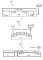


Classifications
-
- G—PHYSICS
- G01—MEASURING; TESTING
- G01N—INVESTIGATING OR ANALYSING MATERIALS BY DETERMINING THEIR CHEMICAL OR PHYSICAL PROPERTIES
- G01N27/00—Investigating or analysing materials by the use of electric, electrochemical, or magnetic means
- G01N27/26—Investigating or analysing materials by the use of electric, electrochemical, or magnetic means by investigating electrochemical variables; by using electrolysis or electrophoresis
- G01N27/403—Cells and electrode assemblies
- G01N27/414—Ion-sensitive or chemical field-effect transistors, i.e. ISFETS or CHEMFETS
- G01N27/4145—Ion-sensitive or chemical field-effect transistors, i.e. ISFETS or CHEMFETS specially adapted for biomolecules, e.g. gate electrode with immobilised receptors
-
- G—PHYSICS
- G01—MEASURING; TESTING
- G01N—INVESTIGATING OR ANALYSING MATERIALS BY DETERMINING THEIR CHEMICAL OR PHYSICAL PROPERTIES
- G01N27/00—Investigating or analysing materials by the use of electric, electrochemical, or magnetic means
- G01N27/26—Investigating or analysing materials by the use of electric, electrochemical, or magnetic means by investigating electrochemical variables; by using electrolysis or electrophoresis
-
- G—PHYSICS
- G01—MEASURING; TESTING
- G01N—INVESTIGATING OR ANALYSING MATERIALS BY DETERMINING THEIR CHEMICAL OR PHYSICAL PROPERTIES
- G01N27/00—Investigating or analysing materials by the use of electric, electrochemical, or magnetic means
- G01N27/60—Investigating or analysing materials by the use of electric, electrochemical, or magnetic means by investigating electrostatic variables, e.g. electrographic flaw testing
-
- G—PHYSICS
- G01—MEASURING; TESTING
- G01N—INVESTIGATING OR ANALYSING MATERIALS BY DETERMINING THEIR CHEMICAL OR PHYSICAL PROPERTIES
- G01N33/00—Investigating or analysing materials by specific methods not covered by groups G01N1/00 - G01N31/00
- G01N33/48—Biological material, e.g. blood, urine; Haemocytometers
- G01N33/50—Chemical analysis of biological material, e.g. blood, urine; Testing involving biospecific ligand binding methods; Immunological testing
-
- G—PHYSICS
- G10—MUSICAL INSTRUMENTS; ACOUSTICS
- G10K—SOUND-PRODUCING DEVICES; METHODS OR DEVICES FOR PROTECTING AGAINST, OR FOR DAMPING, NOISE OR OTHER ACOUSTIC WAVES IN GENERAL; ACOUSTICS NOT OTHERWISE PROVIDED FOR
- G10K11/00—Methods or devices for transmitting, conducting or directing sound in general; Methods or devices for protecting against, or for damping, noise or other acoustic waves in general
- G10K11/16—Methods or devices for protecting against, or for damping, noise or other acoustic waves in general
- G10K11/175—Methods or devices for protecting against, or for damping, noise or other acoustic waves in general using interference effects; Masking sound
-
- H—ELECTRICITY
- H03—ELECTRONIC CIRCUITRY
- H03M—CODING; DECODING; CODE CONVERSION IN GENERAL
- H03M1/00—Analogue/digital conversion; Digital/analogue conversion
- H03M1/06—Continuously compensating for, or preventing, undesired influence of physical parameters
- H03M1/08—Continuously compensating for, or preventing, undesired influence of physical parameters of noise
-
- H—ELECTRICITY
- H10—SEMICONDUCTOR DEVICES; ELECTRIC SOLID-STATE DEVICES NOT OTHERWISE PROVIDED FOR
- H10D—INORGANIC ELECTRIC SEMICONDUCTOR DEVICES
- H10D30/00—Field-effect transistors [FET]
- H10D30/60—Insulated-gate field-effect transistors [IGFET]
- H10D30/68—Floating-gate IGFETs
-
- G—PHYSICS
- G01—MEASURING; TESTING
- G01N—INVESTIGATING OR ANALYSING MATERIALS BY DETERMINING THEIR CHEMICAL OR PHYSICAL PROPERTIES
- G01N27/00—Investigating or analysing materials by the use of electric, electrochemical, or magnetic means
- G01N27/26—Investigating or analysing materials by the use of electric, electrochemical, or magnetic means by investigating electrochemical variables; by using electrolysis or electrophoresis
- G01N27/403—Cells and electrode assemblies
- G01N27/414—Ion-sensitive or chemical field-effect transistors, i.e. ISFETS or CHEMFETS
- G01N27/4148—Integrated circuits therefor, e.g. fabricated by CMOS processing
Definitions
- the invention relates to a bioelectric activity detecting sensor, which can be widely used in biomedical and other technical applications, such as cell activity detection, DNA detection, biological protein detection, drug screening, etc., different implementations of the present invention can be used for voltage signal detection and charge, respectively.
- Signal Detection can be used for voltage signal detection and charge, respectively.
- biomolecular process detection has received increasing attention, such as cell activity detection, DNA detection, biological protein detection, and drug screening.
- direct electrical activity detection has the advantages of simple detection and is convenient for real-time detection.
- solid state traditional biosensors for direct electrical activity detection one is a microelectrode array and the other is a field effect device.
- both conventional sensors require additional reference electrodes to set the voltage difference between the solution and the sensor substrate, which makes large-scale integration of standard integrated circuit processes of conventional sensors difficult, thereby hindering further low cost of such sensors. And portable.
- a floating gate transistor As a common basic unit in a semiconductor device, a floating gate transistor has two ports of a floating gate and a control gate and can be used as an input terminal, and can realize a threshold voltage and a saturation current by a superposition principle of a control gate and a floating gate. control. Therefore, some scholars have proposed devices with floating-gate transistor structures.
- the use of control gates compensates for the lack of additional reference electrodes for conventional sensors. However, the control gate can only be used to set static operating points. In the actual detection process, there are also electrochemical noise caused by ion movement of the electrolyte solution, slow DC drift due to temperature change, and the like. Noise problems suppress or prevent accurate signal detection, so a new type of sensor is needed to overcome this type of noise, make up for the deficiencies of existing sensors, and achieve high signal-to-noise ratio detection.
- the present invention combines the principle of active noise control and the principle of signal superposition to propose a novel sensor which can realize potential or charge detection and has active noise control characteristics, and can realize not only a reference electrode.
- the detection can also effectively suppress the slow DC drift, harmonic noise and wideband noise in the detection, and has the advantages of high signal to noise ratio detection.
- a novel active noise control biosensor includes a detecting plate, a signal detecting module and a control module, wherein the signal detecting module comprises a signal stackable transistor and a reading circuit, and the signal stackable transistor has at least two inputs a secondary input receiving a secondary signal and a primary input receiving a primary signal; the detection plate inputting the detected primary signal to a primary input, the control module processing the output of the signal detection module through a signal processing system Letter And generating a secondary signal input to the secondary input terminal; the primary signal received by the signal stackable transistor and the secondary signal are superimposed to achieve active noise control, and the superposed signal is read by the read circuit And output as an input signal of the control module.
- the signal detecting module comprises a signal stackable transistor and a reading circuit
- the signal stackable transistor has at least two inputs a secondary input receiving a secondary signal and a primary input receiving a primary signal
- the detection plate inputting the detected primary signal to a primary input
- the control module processing the output of the signal detection module through a signal
- a gate and a metal wire are respectively connected to the gate of the signal stackable transistor as a secondary input and a primary input; or two capacitors are simultaneously connected to the gate of the transistor as a primary input and a secondary Input.
- the signal stackable transistor uses a field effect transistor.
- two heavily doped regions are formed on the substrate of the signal stackable transistor as a source terminal and a drain terminal respectively, and a double gate structure is disposed above the substrate, and the first gate structure is a floating gate, the second gate structure is a control gate; the floating gate is separated from the substrate by a dielectric layer, and the upper of the floating gate is separated from the control gate by another dielectric layer; the floating gate passes through the metal line Connected to the detector plate, as a primary input, the control gate acts as a secondary input.
- two heavily doped regions are formed on the substrate of the signal stackable transistor as a source terminal and a drain terminal respectively, and a double gate structure is disposed above the substrate, and the first gate structure is a floating gate, the second gate structure is a column gate structure, including a control gate and a floating gate coupling input end, and an isolation layer is disposed between the control gate and the floating gate coupling input end;
- the dielectric layer is isolated from the substrate, and the upper portion of the floating gate is separated from the second gate structure by another dielectric layer; the floating gate coupling input end is connected to the detecting plate through a metal line as a primary input end,
- the control gate acts as a secondary input.
- two heavily doped regions are respectively formed on the substrate of the signal stackable transistor as a source terminal and a drain terminal, and a single gate gate structure is disposed above the substrate as a floating gate, and the floating gate
- the substrate is separated from the substrate by a dielectric layer; the floating gate is connected with two metal-insulating layers-metal capacitors as primary input and secondary input, respectively.
- two heavily doped regions are respectively formed on the substrate of the signal stackable transistor as a source terminal and a drain terminal, and a single gate gate structure is disposed above the substrate as a floating gate; a side of the bottom, a well is formed along the width of the gate; an isolation layer is disposed between the substrate and the well, and the floating gate is separated from the well and the substrate by a dielectric layer; the well serves as a secondary At the input end, the floating gate is connected to the detecting plate through a metal wire as a primary input terminal; or the well is used as a secondary input terminal, and a metal-insulating layer-metal capacitor is connected to the floating gate as a primary The input terminal; or the well is used as a primary input terminal, and a metal-insulating layer-metal capacitor is connected to the floating gate as a secondary input terminal.
- two heavily doped regions are respectively formed on the substrate of the signal stackable transistor as a source terminal and a drain terminal, and a single gate gate structure is disposed above the substrate as a floating gate;
- Two sides of the bottom side, along the width direction of the gate, are respectively used as a control gate and a floating gate coupling input end;
- an isolation layer is disposed between the substrate and the well, and a floating gate is passed between the well and the substrate.
- the layer dielectric layer is isolated; the floating gate coupling input is connected to the detector plate by a metal line as a primary input, and the control gate serves as a secondary input.
- the control module adopts a non-reference feedforward control module, that is, a known frequency harmonic signal is directly generated inside the control module as a reference required for feedforward control, and the output signal of the signal detection module is processed by feedforward control to generate a second
- the level signal is input to the secondary input end of the signal detecting module; or the control module uses a reference feedforward control module, that is, a reference noise input terminal is extracted from the control module for detecting background noise as a reference for feedforward control Processing the output signal of the signal detecting module by feedforward control to generate a secondary signal input to the secondary input end of the signal detecting module; or the control module adopts a feedback control module to process the signal detecting module by feedback control The output signal produces a secondary signal input to the secondary input of the signal detection module.
- the charge or potential detection can be realized.
- the gate of the signal stackable transistor is directly connected to the detecting plate through the wire, and the charge detection can be realized.
- the gate of the signal stackable transistor is connected to the detecting plate through the capacitor, which can be realized. Potential detection.
- the signal superimposable transistor has a secondary input receiving the secondary signal and a primary input receiving the primary signal, and the output signal can be flexibly controlled by the superposition of two or more inputs, including DC and AC control. .
- the control module can adopt feedforward control or feedback control to achieve slow DC drift, harmonic noise, effective suppression of broadband noise, and flexible control mode.
- FIG. 1 is a schematic diagram of two different structural structures of a signal stackable transistor of the present invention, a) a direct input type transistor for a primary input terminal, and b) a self-contained capacitance type transistor for a primary input terminal.
- FIG. 2 is a diagram showing an example of a double-layered gate structure fabricated in the integrated circuit process of the primary input direct input transistor of FIG. 1a).
- FIG. 3 is a diagram showing an example of a single-layer gate structure fabricated in the integrated circuit process of the primary input direct input transistor of FIG. 1a).
- FIG. 4 is a diagram showing an example of a double-layered gate structure fabricated by the integrated circuit of the primary input terminal of FIG. 1b in an integrated circuit process.
- FIG. 5 is a diagram showing an example of a single-layer gate structure fabricated by the integrated circuit of the primary input terminal of FIG. 1b).
- Figure 6 is a block diagram of a novel active noise control biosensor system of the present invention.
- FIG. 7 is a block diagram of a sensor system in which the control module of the present invention suppresses known harmonic noise using a referenceless feedforward control method.
- FIG. 8 is a schematic diagram of a sensor system of the control module of the present invention using a reference feedforward control method to suppress unpredictable noise.
- FIG. 9 is a schematic diagram of a sensor system in which the control module of the present invention uses a feedback control method to suppress various types of noise.
- Figure 10 is a sensor implementation example of suppressing power frequency interference based on the system of Figure 9.
- Fig. 1 is a structural schematic diagram of a signal superimposable transistor of a core device of the present invention.
- the present invention proposes two signal superimposable transistors of different structures.
- the signal stackable transistor can be understood as a transistor and its gate is controlled by at least two inputs, and one input is a secondary.
- the input terminal controls the gate through a capacitor, and the other input terminal is the primary input terminal, which can control the gate by directly controlling the charge transfer through the metal wire, as shown in FIG. 1a), or through the capacitor.
- the regulation of the gate is realized as shown in Fig. 1b).
- the invention mainly utilizes the above two input terminals to input the primary signal and the secondary signal, and cancels the superposition of the noise in the two input signals to cancel the active noise control.
- the signal stackable transistor 101 in FIG. 1a) is referred to as a primary input direct input type transistor
- the signal stackable transistor 102 in FIG. 1b) is a primary input terminal self-contained capacitor type transistor. Used for charge and potential detection, respectively.
- a floating gate transistor As a common basic unit in a semiconductor device, a floating gate transistor has two ports of a floating gate and a control gate and can be used as an input terminal, and can realize a threshold voltage and a saturation current by a superposition principle of a control gate and a floating gate. control.
- the present invention will provide several types of floating gate transistors to implement signal superimposable transistors. The following will be described in detail with reference to FIGS. 2 to 5 in several specific embodiments.
- the transistor 20 has a two-layer gate structure, which is prepared by forming two heavily doped regions on the substrate 28 as the source terminal 27 and the drain terminal 26; the floating gate 22 is a first layer gate structure, and the lower layer passes through a layer
- the dielectric layer 25 is isolated from the substrate and is isolated from the control gate 23 by another dielectric layer 24, which is a second gate structure.
- the most important feature of the structure is that the floating gate 22 connects the metal wires through the contact holes and directly leads to the external detecting plate 21.
- the floating gate 22 and the control gate 23 Each of the materials to be produced may be any one of polycrystalline silicon, metal, organic conductor, and the like.
- the control gate 23 of the transistor 20 acts as a secondary input
- the floating gate 22 acts as a primary input
- the detection plate 21 is the detector plate.
- the transistor 30 has a single-layer gate structure in which two heavily doped regions are formed on the substrate 37 as the source terminal 35 and the drain terminal 36, and a well 33 is formed on the side of the substrate 37 by ion implantation.
- the control gate, the positional relationship between the well 33 and the substrate 37 are juxtaposed along the gate width direction, and isolation between the two is required; and a single layer gate 32 is used as a floating gate over the well 33 and the substrate 37.
- the single layer gate 32 is isolated from the well 33 and the substrate 37 by a dielectric layer 34.
- the single-layer grid 32 is connected to the metal wires through the contact holes and directly led out to the external detecting plate 31.
- the material for forming the single-layered gate 32 may be any one of polysilicon, metal, organic conductor, and the like.
- the control gate 33 in the transistor 30 acts as a secondary input
- the floating gate 32 acts as a primary input
- the detection plate 31 is the detector plate.
- the transistor 40 has a double-layered gate structure, which is prepared by forming two heavily doped regions on the substrate 48 as a source terminal 47 and a drain terminal 46.
- the floating gate 42 is a first layer gate structure and a dielectric layer is passed underneath.
- the layer 45 is isolated from the substrate 48, and is separated from the second layer by another dielectric layer 44.
- the second gate is a column gate structure, that is, two gates are respectively formed above the floating gate 42: the control gate 43 and the floating gate
- the input terminal 49 is coupled, and the two gates are separated by a dielectric layer.
- the floating gate coupling input terminal 49 is connected to the metal line through the contact hole and led out to the external detecting plate 41.
- the material of the first layer gate and the second layer gate may be any one of polysilicon, metal, organic conductor, and the like.
- the control gate 43 of the transistor 40 acts as a secondary input
- the floating gate coupling input 49 acts as a primary input
- the detection plate 41 is the detector plate.
- FIG. 5 is a diagram showing an example of a single-layer gate structure fabricated by an integrated circuit process in a primary input terminal of FIG. 1b), which mainly illustrates several methods for preparing a coupling capacitor.
- transistor 501 uses two wells as the control gate and floating gate coupling input.
- transistor 502 uses two metal-insulator-metal capacitors (MIM capacitors) as control gate and floating gate coupling inputs.
- the transistor 503 in Figure 5c) uses a well and a metal-insulating layer-metal capacitor (MIM capacitor) as the control gate and floating gate coupling input, respectively, and the two are interchangeable.
- MIM capacitor metal-insulating layer-metal capacitor
- the control gates of the above three types of transistors act as secondary input terminals
- the floating gate coupling input acts as the primary input
- the detection plate is the detector plate.
- the main body parts of the above three types of transistors are similarly fabricated by forming two heavily doped regions on the substrate as source and drain terminals, a single layer gate as a floating gate, and a dielectric layer between the floating gate and the substrate. isolation.
- the method of preparing the well capacitor is as follows: in the gate width direction extension line, a well is formed by ion implantation on the side of the substrate, a single layer The gate is extended to form an overlap region with the well above the well, and the overlap region is separated by a dielectric layer, and the formed capacitor is a well capacitor; the metal-insulating layer-metal capacitor (MIM capacitor) is prepared as follows: : Two different metal layers are separated by an insulating layer, and the formed capacitance is a MIM capacitor.
- MIM capacitor metal-insulating layer-metal capacitor
- Figure 1 depicts two principles of the core device of the present invention, which have in common: both are transistors having at least two input ports, and two ports are used for signal superposition, called signal stackable transistors; The difference is whether the primary input has a coupling capacitor.
- Figure 2 and Figure 3 are respectively an example of the implementation of the direct input type transistor of the primary input terminal in Figure 1a) under different process conditions, which can be used for charge detection;
- Figure 4 and Figure 5 are the self-contained capacitance type of the primary input terminal in Figure 1b).
- An example of the implementation of a transistor under different process conditions can be used for potential detection. It should be noted that the embodiment of the transistor based on the principle of FIG. 1a) and FIG. 1b) of the present invention is not limited to the solutions in the several embodiments described above.
- FIG. 6 is a system frame diagram of a novel active noise control biosensor of the present invention.
- the novel active noise control biosensor 60 is mainly composed of three parts, namely a signal detection module 61, a detection plate 63 and a control module 62.
- the signal detecting module 61 is composed of a signal stackable transistor and a read circuit.
- the signal stackable transistor has at least two inputs, including a secondary input receiving the secondary signal and a primary input receiving the primary signal.
- the stage input signal and the primary input signal are superimposed in the signal detection and measurement module 61 to realize active noise control, and the superimposed signal is read and output by the reading circuit in the signal detection module 61, and serves as an input signal of the control module 62;
- the detecting plate 63 is connected to the sample to be tested, and the primary signal is input to the primary input end of the signal detecting module 61;
- the control module 62 processes the output signal of the signal detecting module 61 through the signal processing system to generate a secondary signal input to the signal detecting.
- the signal stackable transistor in the signal detecting module 61 can adopt any one of the two principles in FIG. 1, and any one of the above embodiments can be used; the read circuit can be a source when the transistor is turned on.
- the stage follows any one of the amplifying and reading circuits such as the amplifying circuit or the common source amplifying circuit; the control module 62 can adopt two methods of feedforward control and feedback control, and the feedforward control can be further divided into reference feedforward control and no Referring to feedforward control, the different control methods are described in detail below.
- the sensor 70 is mainly composed of a signal detecting module 71, a detecting plate 73 and a feedforward control module 72.
- the signal detecting module 71 is composed of a signal stackable transistor and a read circuit.
- the signal stackable transistor may be a direct input type transistor of the primary input terminal or a self-contained capacitor type transistor of the primary input terminal.
- the signal stackable transistor has two inputs, a secondary input for receiving the secondary signal and a primary input for receiving the primary signal;
- the read circuit refers to the source-level following amplification circuit after the transistor is turned on or Any one of the read circuits such as the common source amplifier circuit performs signal reading.
- the control gate input signal and the floating gate input signal can be read at the source or drain of the transistor.
- the output signal generated by the superposition; the detecting plate 73 is connected to the sample to be tested, and the detecting primary signal is input to the primary input end of the signal detecting module 71; the feedforward control module 72 can predict the primary noise in advance.
- a known frequency harmonic signal is directly generated inside the control module as a reference for feedforward control, and an output signal of the signal detection module 71 is processed by feedforward control to generate a secondary signal input to the signal detection module 71. Secondary input. The secondary input signal and the primary input signal are superimposed in the signal detecting module 71, thereby reducing the output noise of the reading circuit in the signal detecting module 71, and realizing active noise reduction of the primary harmonic noise.
- the premise of this type of sensor is that the noise needs to be predictable harmonic noise.
- FIG. 8 is a schematic diagram of a sensor system of the control module of the present invention using a reference feedforward control method to suppress unpredictable noise.
- the composition and working principle of the sensor 80 are similar to those of the sensor 70 described above, except that the feedforward control module 82 draws a reference noise input 84 for detecting background noise as a reference for feedforward control.
- the noise signal in the primary signal is a non-predictable signal, including slow DC drift, harmonics and wideband noise.
- the feedforward control module 82 processes the output signal of the signal detection module 81 through the feedforward control to generate a secondary signal input to the secondary input of the signal detection module 81.
- the signal stackable transistor in the signal detecting module 81 can also adopt one of the above-mentioned primary input direct input type transistor and the primary input end self-contained capacitive type transistor, and the read circuit is the same as the above sensor 70.
- the detecting plate 83 is connected to the sample to be tested, and the primary signal is detected to be input to the primary input of the signal detecting module 81.
- the secondary input signal and the primary input signal are superimposed in the signal detection module 81, thereby reducing the output noise of the read circuit in the signal detection module 81, and achieving active noise reduction for the primary noise.
- FIG. 9 is a schematic diagram of a sensor system in which the control module of the present invention uses a feedback control method to suppress various types of noise.
- the sensor 90 differs from the sensor 70 and sensor 80 described above in that the sensor 90 employs a feedback control module 92, regardless of the type of primary noise signal, including slow DC drift, harmonics, and broadband noise.
- the signal detecting module 91 and the sensor signal detecting modules 71 and 81 are completely identical, and the configuration of the signal stackable transistor is optional, and the setting of the reading circuit is all the same.
- the detecting plate 93 is connected to the sample to be tested, the primary signal is detected and input to the primary input end of the signal detecting module 91, the reading circuit reads the output signal and inputs the output signal to the feedback control module 92, after feedback
- the feedback control of the control module 92 processes the output signal of the signal detection module 91 to produce a secondary signal input to the secondary input of the signal detection module 91.
- a secondary signal is obtained and input to the secondary input of the signal detection module 91.
- the primary input signal and the secondary input signal are superimposed in the signal detection module 91, thereby reducing the output noise of the read circuit in the signal detection module 91, and achieving active noise reduction for the primary noise.
- Figure 10 is an embodiment of the sensor 90 of Figure 9.
- the purpose of the sensor 100 is to suppress 50 Hz power frequency interference in the primary signal, that is, the primary noise is 50 Hz power frequency interference.
- the sensor 100 is self-charged with the primary input of Figure 1b)
- the signal superimposable transistor 101 can have two capacitors on the gate of one field effect transistor, one capacitor is a self-contained capacitor of the primary input terminal, and is connected to the detecting plate 105; the other is the control gate capacitor. .
- the specific implementation of the read circuit is to apply a turn-on voltage on the control gate, apply a positive voltage at the drain terminal to ensure that the transistor is in a saturated working region, and connect the current mirror 102 to the source terminal to achieve the source-level follow-up output, thereby causing the source to output a signal. It changes as the voltage signal on the floating gate changes.
- the voltage signal detected by the detecting plate 105 is input to the gate of the transistor through the primary input terminal and outputted by the above-mentioned reading circuit, and the output signal is processed by the feedback control module to generate a secondary signal, and the secondary signal is generated. Input to the secondary input of the transistor.
- the primary input signal and the secondary input signal are superimposed in the transistor to achieve active noise reduction.
- the feedback control module of the sensor 100 includes a band pass filter 103 and an inverting amplifier 104 having a center frequency of 50 Hz, and the noise suppression effect can be adjusted by adjusting the center frequency and the quality factor of the band pass filter and the gain of the inverting amplifier.
Landscapes
- Health & Medical Sciences (AREA)
- Life Sciences & Earth Sciences (AREA)
- Physics & Mathematics (AREA)
- Chemical & Material Sciences (AREA)
- Engineering & Computer Science (AREA)
- Molecular Biology (AREA)
- Immunology (AREA)
- Pathology (AREA)
- Analytical Chemistry (AREA)
- General Physics & Mathematics (AREA)
- General Health & Medical Sciences (AREA)
- Biochemistry (AREA)
- Electrochemistry (AREA)
- Chemical Kinetics & Catalysis (AREA)
- Acoustics & Sound (AREA)
- Multimedia (AREA)
- Biomedical Technology (AREA)
- Hematology (AREA)
- Urology & Nephrology (AREA)
- Microelectronics & Electronic Packaging (AREA)
- Spectroscopy & Molecular Physics (AREA)
- Biotechnology (AREA)
- Medicinal Chemistry (AREA)
- Food Science & Technology (AREA)
- Cell Biology (AREA)
- Microbiology (AREA)
- Theoretical Computer Science (AREA)
- Amplifiers (AREA)
- Semiconductor Integrated Circuits (AREA)
- Investigating Or Analyzing Materials By The Use Of Electric Means (AREA)
Abstract
一种新型主动噪声控制生物传感器(60,70,80,90),其包括探测极板(63,73,83,93)、信号检测模块(61, 71,81,91)和控制模块(62,72,82,92)。信号检测模块(61,71,81,91)包括信号可叠加型晶体管(101,102,10,20,30,501,502,503)和读取电路。信号可叠加型晶体管(101, 102, 10, 20, 30, 501, 502, 503)具有次级输入端和初级输入端;探测极板(63,73,83,93)将检测到的初级信号输入到初级输入端,控制模块(62,72,82,92)通过信号处理系统处理信号检测模块(61,71,81,91)的输出信号,并产生次级信号输入到次级输入端;信号可叠加型晶体管(101, 102, 10, 20, 30, 501, 502, 503)接收到的初级信号与次级信号产生叠加作用实现主动噪声控制,叠加后的信号由读取电路读取并输出,作为控制模块(62,72,82,92)的输入信号。该传感器可以实现电位或电荷检测,具有主动噪声控制特性,不仅可以实现无参考电极检测,还可以有效抑制检测中的直流漂移,谐波噪声和宽带噪声,具有高信噪比检测的优点。
Description
本发明涉及一种生物电活动检测传感器,可广泛用于生物医学等技术应用,比如细胞活动检测、DNA检测、生物蛋白检测、药物筛选等,本发明不同实施可分别用于电压信号检测和电荷信号检测。
近年来,生物分子过程检测越来越受到关注,如细胞活动检测、DNA检测、生物蛋白检测、药物筛选等。相对于光学检测,直接电活动检测具有检测简单等优点,便于实现活体检测。目前,直接电活动检测主要有两种固态传统生物传感器,一种是微电极阵列,一种是场效应器件。然而,这两种传统传感器均需要额外的参考电极来设置溶液与传感器衬底之间的压差,这导致传统传感器的标准集成电路工艺大规模集成困难,进而阻碍了这类传感器的进一步低成本化和便携化。
浮栅晶体管作为半导体器件中的一个常见基础单元,具有浮栅和控制栅两个端口且均可以被用作输入端,并且可以通过控制栅和浮栅的叠加原理实现对阈值电压和饱和电流的控制。因此,有学者提出了类浮栅晶体管结构的器件,通过控制栅的使用弥补了传统传感器需要额外参考电极的不足,然而控制栅仅可以用来设置静态工作点。在实际检测过程中,还存在着因电解质溶液离子运动导致的电化学噪声、因温度变化引起的缓慢直流漂移等。噪声问题抑制或阻止了准确的信号检测,因此需要一种新型传感器来克服这类噪声,弥补现有传感器的不足,实现高信噪比的检测。
发明内容
为了克服上述现有技术中存在的不足,本发明结合主动噪声控制原理和信号叠加原理,提出一种新型传感器,该传感器可以实现电位或电荷检测,具有主动噪声控制特性,不仅可以实现无参考电极检测,还可以有效抑制检测中的缓慢直流漂移、谐波噪声和宽带噪声,具有高信噪比检测的优点。
本发明采用的技术方案如下:
一种新型主动噪声控制生物传感器,包括探测极板、信号检测模块和控制模块,其特征在于,信号检测模块包括信号可叠加型晶体管以及读取电路,信号可叠加型晶体管具有至少两个输入端,包括接收次级信号的次级输入端和接收初级信号的初级输入端;所述探测极板将探测的初级信号输入到初级输入端,所述控制模块通过信号处理系统处理信号检测模块的输出信
号,并产生次级信号输入到次级输入端;所述信号可叠加型晶体管接收到的初级信号与次级信号产生叠加作用实现主动噪声控制,叠加后的信号由所述读取电路读取并输出,作为所述控制模块的输入信号。
所述信号可叠加型晶体管的栅极上同时连接一个电容和一根金属导线分别作为次级输入端和初级输入端;或者晶体管的栅极上同时连接两个电容分别作为初级输入端和次级输入端。
进一步地,所述信号可叠加型晶体管采用场效应晶体管。
另一种技术方案,所述信号可叠加型晶体管的衬底上生成有两个重型掺杂区分别作为源端和漏端,在衬底上方设有双层栅结构,第一层栅结构为浮栅,第二层栅结构为控制栅;所述浮栅的下方通过一层介质层与衬底隔离,浮栅的上方通过另一层介质层与控制栅隔离;所述浮栅通过金属线与所述探测极板连接,作为初级输入端,所述控制栅作为次级输入端。
另一种技术方案,所述信号可叠加型晶体管的衬底上生成有两个重型掺杂区分别作为源端和漏端,在衬底上方设有双层栅结构,第一层栅结构为浮栅,第二层栅结构为分列栅结构,包括控制栅和浮栅耦合输入端,所述控制栅和浮栅耦合输入端之间设有隔离层;所述浮栅的下方通过一层介质层与衬底隔离,浮栅的上方通过另一层介质层与第二层栅结构隔离;所述浮栅耦合输入端通过金属线与所述探测极板连接,作为初级输入端,所述控制栅作为次级输入端。
另一种技术方案,所述信号可叠加型晶体管的衬底上生成有两个重型掺杂区分别作为源端和漏端,在衬底上方设有单层栅结构用作浮栅,浮栅与衬底之间通过一层介质层隔离;所述浮栅上连接有两个金属—绝缘层—金属电容,分别作为初级输入端和次级输入端。
另一种技术方案,所述信号可叠加型晶体管的衬底上生成有两个重型掺杂区分别作为源端和漏端,在衬底上方设有单层栅结构用作浮栅;在衬底的侧边、沿着栅宽方向生成一个阱;所述衬底与阱之间设有隔离层,浮栅与阱和衬底之间通过一层介质层进行隔离;所述阱作为次级输入端,所述浮栅通过金属线与所述探测极板连接,作为初级输入端;或者所述阱作为次级输入端,所述浮栅上连接有金属—绝缘层—金属电容,作为初级输入端;或者所述阱作为初级输入端,所述浮栅上连接有金属—绝缘层—金属电容,作为次级输入端。
另一种技术方案,所述信号可叠加型晶体管的衬底上生成有两个重型掺杂区分别作为源端和漏端,在衬底上方设有单层栅结构用作浮栅;在衬底的侧边、沿着栅宽方向生成两个阱分别用作控制栅和浮栅耦合输入端;所述衬底与阱之间设有隔离层,浮栅与阱和衬底之间通过一层介质层进行隔离;所述浮栅耦合输入端通过金属线与所述探测极板连接,作为初级输入端,所述控制栅作为次级输入端。
所述控制模块采用无参考前馈控制模块,即在控制模块内部直接产生已知频率谐波信号作为前馈控制所需的参考,通过前馈控制处理所述信号检测模块的输出信号,产生次级信号输入到所述信号检测模块的次级输入端;或者控制模块采用有参考前馈控制模块,即从控制模块中引出一个参考噪声输入端用于探测背景噪声作为前馈控制所需的参考,通过前馈控制处理所述信号检测模块的输出信号,产生次级信号输入到所述信号检测模块的次级输入端;或者控制模块采用反馈控制模块,通过反馈控制处理所述信号检测模块的输出信号,产生次级信号输入到所述信号检测模块的次级输入端。
本发明提出的新型主动噪声控制生物传感器的显著优点在于:
(1)可以实现电荷或电位检测,信号可叠加型晶体管的栅极直接通过导线与探测极板相连,可以实现电荷检测,信号可叠加型晶体管的栅极通过电容与探测极板相连,可以实现电位检测。
(2)信号可叠加型晶体管具有接收次级信号的次级输入端和接收初级信号的初级输入端,通过两个或多输入端的叠加作用可以灵活实现输出信号的控制,包括直流和交流的控制。
(3)控制模块可以采用前馈控制或反馈控制实现缓慢直流漂移,谐波噪声,宽带噪声的有效抑制,控制方式灵活。
(4)不仅可以实现无参考电极检测,还可以有效抑制检测中的缓慢直流漂移、谐波噪声和宽带噪声,实现高信噪比检测。
图1是本发明信号可叠加型晶体管的两种不同的结构原理图,a)为初级输入端直接输入型晶体管,b)为初级输入端自带电容型晶体管。
图2是图1a)中初级输入端直接输入型晶体管在集成电路工艺下制作的双层栅结构的示例图。
图3是图1a)中初级输入端直接输入型晶体管在集成电路工艺下制作的单层栅结构的示例图。
图4是图1b)中初级输入端自带电容型晶体管在集成电路工艺下制作的双层栅结构的示例图。
图5是图1b)中初级输入端自带电容型晶体管在集成电路工艺下制作的单层栅结构的示例图。
图6是本发明新型主动噪声控制生物传感器系统框架图。
图7是本发明控制模块采用无参考前馈控制方式抑制已知谐波噪声的传感器系统框架图。
图8是本发明控制模块采用有参考前馈控制方式抑制不可提前预知性噪声的传感器系统框架图。
图9是本发明控制模块采用反馈控制方式抑制各类噪声的传感器系统框架图。
图10是基于图9系统的抑制工频干扰的一个传感器实施实例。
为使本发明的内容更加清楚,下面将结合附图对本发明实施方式作进一步的描述。
图1是本发明核心器件信号可叠加型晶体管的结构原理图。本发明提出两种不同结构的信号可叠加型晶体管,从原理上理解,该信号可叠加型晶体管可理解为一个晶体管且其栅极受控于至少两个输入端的调控,一个输入端为次级输入端,通过一个电容实现对栅极的调控,另一个输入端为初级输入端,可以是直接通过金属导线控制电荷转移实现对栅极的调控,如图1a)所示,也可以是通过电容实现对栅极的调控,如图1b)所示。本发明主要利用上述两个输入端,进行初级信号和次级信号的输入,并使两输入信号中的噪声产生叠加作用相互抵消,实现主动噪声控制。为便于描述,称图1a)中的信号可叠加型晶体管101为初级输入端直接输入型晶体管,图1b)中的信号可叠加型晶体管102为初级输入端自带电容型晶体管,这两种晶体管分别用于电荷和电位检测。
对于图1中两种原理的器件的实现,可以采用多种形式,最基础的方法是采用一个基本的场效应晶体管,在其栅上连接一个电容和一个导线分别作为次级输入端和初级输入端,对应图1a)原理;或是在其栅上连接两个电容分别作为初级输入端和次级输入端,对应图1b)原理。但是上述方法难以实现内部集成,下面将描述更巧妙的方法,可实现电容的内部集成。浮栅晶体管作为半导体器件中的一个常见基础单元,具有浮栅和控制栅两个端口且均可以被用作输入端,并且可以通过控制栅和浮栅的叠加原理实现对阈值电压和饱和电流的控制。本发明将提出几种类浮栅晶体管实现信号可叠加型晶体管,下面将结合图2~图5用几个具体实施示例对图1作详细说明。
图2是图1a)中初级输入端直接输入型晶体管在集成电路工艺下制作的双层栅结构的示例图。该晶体管20具有两层栅的结构,制备方法为:在衬底28上生成两个重型掺杂区作为源端27和漏端26;浮栅22为第一层栅结构,其下方通过一层介质层25与衬底隔离,上方通过另一层介质层24与控制栅23隔离,该控制栅23为第二层栅结构。本结构最主要特点是浮栅22通过接触孔连接金属线,并直接引出到外部探测极板21上。其中,浮栅22、控制栅23的
制作材料均可以是多晶硅、金属、有机导电体等中的任一种。与图1a)对应的,晶体管20中控制栅23充当了次级输入端的角色,浮栅22充当了初级输入端的角色,探测极板21即为探测极板。
图3是图1a)中初级输入端直接输入型晶体管在集成电路工艺下制作的单层栅结构的示例图。该晶体管30具有单层栅的结构,制备方法为:在衬底37上生成两个重型掺杂区作为源端35和漏端36,在衬底37侧边通过离子注入生成一个阱33用作控制栅,阱33和衬底37之间的位置关系是沿着栅宽方向并列,两者之间需要做好隔离;阱33和衬底37上方为一层单层栅32用作浮栅,单层栅32与阱33和衬底37之间通过一层介质层34进行隔离。单层栅32上通过接触孔与金属线相连并直接引出到外部探测极板31。其中,单层栅32的制作材料可以是多晶硅、金属、有机导电体等中的任一种。与图1a)对应的,晶体管30中控制栅33充当了次级输入端的角色,浮栅32充当了初级输入端的角色,探测极板31即为探测极板。
图4是图1b)中初级输入端自带电容型晶体管在集成电路工艺下制作的双层栅结构的示例图。该晶体管40具有双层栅结构,制备方法为:在衬底48上生成两个重型掺杂区作为源端47和漏端46,浮栅42为第一层栅结构,其下方通过一层介质层45与衬底48隔离,上方通过另一层介质层44与第二层栅隔离;第二层栅为分列栅结构,即浮栅42上方分别制作两个栅:控制栅43和浮栅耦合输入端49,这两个栅之间由介质层隔离。浮栅耦合输入端49上通过接触孔与金属线相连并引出到外部探测极板41。其中,第一层栅和第二层栅的制作材料均可以是多晶硅、金属、有机导电体等中的任一种。与图1b)对应的,晶体管40中控制栅43充当了次级输入端的角色,浮栅耦合输入端49充当了初级输入端的角色,探测极板41即为探测极板。
图5是图1b)中初级输入端自带电容型晶体管在集成电路工艺下制作的单层栅结构的示例图,主要表征几种制备耦合电容的方法。图5a)中晶体管501采用两个阱分别作为控制栅和浮栅耦合输入端,图5b)中晶体管502采用两个金属—绝缘层—金属电容(MIM电容)分别作为控制栅和浮栅耦合输入端,图5c)中晶体管503采用一个阱和一个金属—绝缘层—金属电容(MIM电容),分别作为控制栅和浮栅耦合输入端且两者可互换。与图1b)对应的,上述三类晶体管中的控制栅充当了次级输入端的角色,浮栅耦合输入端充当了初级输入端的角色,探测极板即为探测极板。上述三类晶体管主体部分的制作过程相似,都是在衬底上生成两个重型掺杂区作为源端和漏端,单层栅作为浮栅,浮栅与衬底之间通过一层介质层隔离。涉及到阱电容的制备方法如下:在栅宽方向延长线上,于衬底侧边通过离子注入生成一个阱,单层
栅延长至阱上方与阱形成交叠区域,交叠区域之间通过一层介质层隔离,所形成的电容即为阱电容;涉及到金属—绝缘层—金属电容(MIM电容)的制备方法如下:两层不同的金属层之间通过绝缘层隔离,形成的电容为MIM电容。
图1描述了本发明中核心器件的两种原理,两者的共同点:都是具有至少两个输入端口的晶体管,两个端口用于信号的叠加,称为信号可叠加型晶体管;两者的区别在于初级输入端是否带有一个耦合电容。图2、图3分别是图1a)中初级输入端直接输入型晶体管在不同工艺条件下的实施示例,可用于电荷检测;图4、图5分别是图1b)中初级输入端自带电容型晶体管在不同工艺条件下的实施示例,可用于电位检测。需要说明的是,基于本发明图1a)、图1b)原理的晶体管的实施方案,不局限于上述几种实施示例中的方案。
图6为本发明新型主动噪声控制生物传感器的系统框架图。该新型主动噪声控制生物传感器60主要由三个部分组成,分别是信号检测模块61,探测极板63和控制模块62。信号检测模块61由一个信号可叠加型晶体管和读取电路组成,该信号可叠加型晶体管至少有两个输入端,包括接收次级信号的次级输入端和接收初级信号的初级输入端,次级输入信号与初级输入信号在信号检测测模块61中产生叠加作用实现主动噪声控制,叠加后的信号由信号检测模块61中的读取电路读取并输出,同时作为控制模块62的输入信号;探测极板63用于与被测样品连接,探测初级信号输入到信号检测模块61的初级输入端;控制模块62通过信号处理系统处理信号检测模块61的输出信号,产生次级信号输入到信号检测模块61的次级输入端。其中,信号检测模块61中的信号可叠加型晶体管可以采用图1中两种原理的任意一种,可以采用上述实施示例中的任一晶体管;读取电路是在晶体管开启状态下,可以采用源级跟随放大电路或共源放大电路等放大读取电路中的任意一种电路;控制模块62可以采取前馈控制和反馈控制两种方式,前馈控制又可分为有参考前馈控制和无参考前馈控制两种,下面将详细描述不同的控制方式。
图7是本发明控制模块采用无参考前馈控制方式抑制已知谐波噪声的传感器系统框架图。该传感器70主要由信号检测模块71、探测极板73和前馈控制模块72组成。信号检测模块71由一个信号可叠加型晶体管和读取电路组成,该信号可叠加型晶体管可以是上述初级输入端直接输入型晶体管,也可以是上述初级输入端自带电容型晶体管。该信号可叠加型晶体管有两个输入端,分别为接收次级信号的次级输入端和接收初级信号的初级输入端;读取电路是指使晶体管进入开启状态后,采用源级跟随放大电路或共源放大电路等读取电路中的任意一种进行信号读取。在上述读取条件下,可以在晶体管源端或漏端读取到控制栅输入信号和浮栅输入信号
经过叠加产生的输出信号;探测极板73用于与被测样品连接,探测初级信号输入到所述信号检测模块71的初级输入端;前馈控制模块72,可通过提前预判初级噪声的方式,在控制模块内部直接产生已知频率谐波信号作为前馈控制所需的参考,通过前馈控制处理所述信号检测模块71的输出信号,产生次级信号输入到所述信号检测模块71的次级输入端。上述次级输入信号与初级输入信号在所述信号检测模块71中产生叠加作用,从而降低所述信号检测模块71中读取电路的输出噪声,实现对初级谐波噪声的主动降噪。该类传感器的工作前提就是噪声需要是可预知性的谐波噪声。
图8是本发明控制模块采用有参考前馈控制方式抑制不可提前预知性噪声的传感器系统框架图。该传感器80的组成和工作原理均与上述传感器70相差不大,区别在于前馈控制模块82多引出一个参考噪声输入端84,用于探测背景噪声作为前馈控制所需的参考。初级信号中的噪声信号为不可提前预知性信号,包括缓慢的直流漂移,谐波和宽带噪声。前馈控制模块82通过前馈控制处理信号检测模块81的输出信号,产生次级信号输入到信号检测模块81的次级输入端。信号检测模块81中的信号可叠加型晶体管同样可采用上述初级输入端直接输入型晶体管和上述初级输入端自带电容型晶体管两类结构中的一种,读取电路和上述传感器70的相同。探测极板83用于与被测样品连接,探测初级信号输入到信号检测模块81的初级输入端。上述次级输入信号与初级输入信号在信号检测模块81中产生叠加作用,从而降低信号检测模块81中读取电路的输出噪声,实现对初级噪声的主动降噪。
图9是本发明控制模块采用反馈控制方式抑制各类噪声的传感器系统框架图。该传感器90与上述传感器70和传感器80的差别在于该传感器90采用反馈控制模块92,无论初级噪声信号是何种类型,包括缓慢的直流漂移,谐波和宽带噪声。而信号检测模块91和上述传感器信号检测模块71、81完全相同,包括信号可叠加型晶体管的结构的可选性、读取电路的设置全部相同。工作时,探测极板93用于与被测样品连接,探测初级信号输入到信号检测模块91的初级输入端,读取电路读取输出信号并将该输出信号输入到反馈控制模块92,经过反馈控制模块92的反馈控制处理信号检测模块91的输出信号,产生次级信号输入到所述信号检测模块91的次级输入端。得到次级信号并输入到所述信号检测模块91的次级输入端。上述初级输入信号与次级输入信号在信号检测模块91中产生叠加作用,从而降低信号检测模块91中读取电路的输出噪声,实现对初级噪声的主动降噪。
图10是图9所述传感器90的一个实施实例。该传感器100的目的是抑制初级信号中的50Hz工频干扰,即初级噪声为50Hz工频干扰。该传感器100采用图1b)初级输入端自带电
容型晶体管原理,该信号可叠加型晶体管101可以为一个场效应晶体管栅极上带两个电容,一个电容为初级输入端自带电容,其与探测极板105相连;另一个为控制栅电容。读取电路的具体实施是在控制栅上施加一个开启电压,在漏端施加一个正电压,保证晶体管处于饱和工作区,源端连接电流镜102,实现源级跟随输出,从而使源端输出信号跟随浮栅上的电压信号变化而变化。探测极板105探测到的电压信号通过初级输入端自带电容输入到晶体管的栅极并通过上述读取电路输出信号,该输出信号经由反馈控制模块处理产生次级信号,并将该次级信号输入到晶体管的次级输入端。上述初级输入信号与次级输入信号在晶体管中产生叠加作用,实现主动降噪。所述传感器100的反馈控制模块包括中心频率为50Hz的带通滤波器103和反相放大器104,可通过调整带通滤波器的中心频率和品质因数以及反相放大器的增益调整噪声抑制效果。
Claims (9)
- 一种新型主动噪声控制生物传感器,包括探测极板、信号检测模块和控制模块,其特征在于,信号检测模块包括信号可叠加型晶体管以及读取电路,信号可叠加型晶体管具有至少两个输入端,包括接收次级信号的次级输入端和接收初级信号的初级输入端;所述探测极板将探测的初级信号输入到初级输入端,所述控制模块通过信号处理系统处理信号检测模块的输出信号,并产生次级信号输入到次级输入端;所述信号可叠加型晶体管接收到的初级信号与次级信号产生叠加作用实现主动噪声控制,叠加后的信号由所述读取电路读取并输出,作为所述控制模块的输入信号。
- 根据权利要求1所述的一种新型主动噪声控制生物传感器,其特征在于,所述信号可叠加型晶体管的栅极上同时连接一个电容和一根金属导线分别作为次级输入端和初级输入端;或者晶体管的栅极上同时连接两个电容分别作为初级输入端和次级输入端。
- 根据权利要求1或2所述的一种新型主动噪声控制生物传感器,其特征在于,所述信号可叠加型晶体管采用场效应晶体管。
- 根据权利要求1或2所述的一种新型主动噪声控制生物传感器,其特征在于,所述信号可叠加型晶体管的衬底上生成有两个重型掺杂区分别作为源端和漏端,在衬底上方设有双层栅结构,第一层栅结构为浮栅,第二层栅结构为控制栅;所述浮栅的下方通过一层介质层与衬底隔离,浮栅的上方通过另一层介质层与控制栅隔离;所述浮栅通过金属线与所述探测极板连接,作为初级输入端,所述控制栅作为次级输入端。
- 根据权利要求1或2所述的一种新型主动噪声控制生物传感器,其特征在于,所述信号可叠加型晶体管的衬底上生成有两个重型掺杂区分别作为源端和漏端,在衬底上方设有双层栅结构,第一层栅结构为浮栅,第二层栅结构为分列栅结构,包括控制栅和浮栅耦合输入端,所述控制栅和浮栅耦合输入端之间设有隔离层;所述浮栅的下方通过一层介质层与衬底隔离,浮栅的上方通过另一层介质层与第二层栅结构隔离;所述浮栅耦合输入端通过金属线与所述探测极板连接,作为初级输入端,所述控制栅作为次级输入端。
- 根据权利要求1或2所述的一种新型主动噪声控制生物传感器,其特征在于,所述信号可叠加型晶体管的衬底上生成有两个重型掺杂区分别作为源端和漏端,在衬底上方设有单层栅结构用作浮栅,浮栅与衬底之间通过一层介质层隔离;所述浮栅上连接有两个金属—绝缘层—金属电容,分别作为初级输入端和次级输入端。
- 根据权利要求1或2所述的一种新型主动噪声控制生物传感器,其特征在于,所述信号可叠加型晶体管的衬底上生成有两个重型掺杂区分别作为源端和漏端,在衬底上方设有单层 栅结构用作浮栅;在衬底的侧边、沿着栅宽方向生成一个阱;所述衬底与阱之间设有隔离层,浮栅与阱和衬底之间通过一层介质层进行隔离;所述阱作为次级输入端,所述浮栅通过金属线与所述探测极板连接,作为初级输入端;或者所述阱作为次级输入端,所述浮栅上连接有金属—绝缘层—金属电容,作为初级输入端;或者所述阱作为初级输入端,所述浮栅上连接有金属—绝缘层—金属电容,作为次级输入端。
- 根据权利要求1或2所述的一种新型主动噪声控制生物传感器,其特征在于,所述信号可叠加型晶体管的衬底上生成有两个重型掺杂区分别作为源端和漏端,在衬底上方设有单层栅结构用作浮栅;在衬底的侧边、沿着栅宽方向生成两个阱分别用作控制栅和浮栅耦合输入端;所述衬底与阱之间设有隔离层,浮栅与阱和衬底之间通过一层介质层进行隔离;所述浮栅耦合输入端通过金属线与所述探测极板连接,作为初级输入端,所述控制栅作为次级输入端。
- 根据权利要求1或2所述的一种新型主动噪声控制生物传感器,其特征在于,所述控制模块采用无参考前馈控制模块,即在控制模块内部直接产生已知频率谐波信号作为前馈控制所需的参考,通过前馈控制处理所述信号检测模块的输出信号,产生次级信号输入到所述信号检测模块的次级输入端;或者控制模块采用有参考前馈控制模块,即从控制模块中引出一个参考噪声输入端用于探测背景噪声作为前馈控制所需的参考,通过前馈控制处理所述信号检测模块的输出信号,产生次级信号输入到所述信号检测模块的次级输入端;或者控制模块采用反馈控制模块,通过反馈控制处理所述信号检测模块的输出信号,产生次级信号输入到所述信号检测模块的次级输入端。
Priority Applications (1)
| Application Number | Priority Date | Filing Date | Title |
|---|---|---|---|
| US16/322,427 US10697929B2 (en) | 2016-08-15 | 2016-10-20 | Active noise control biosensor |
Applications Claiming Priority (2)
| Application Number | Priority Date | Filing Date | Title |
|---|---|---|---|
| CN201610669750.7 | 2016-08-15 | ||
| CN201610669750.7A CN107764874B (zh) | 2016-08-15 | 2016-08-15 | 一种新型主动噪声控制生物传感器 |
Publications (1)
| Publication Number | Publication Date |
|---|---|
| WO2018032600A1 true WO2018032600A1 (zh) | 2018-02-22 |
Family
ID=61196276
Family Applications (1)
| Application Number | Title | Priority Date | Filing Date |
|---|---|---|---|
| PCT/CN2016/102689 Ceased WO2018032600A1 (zh) | 2016-08-15 | 2016-10-20 | 一种新型主动噪声控制生物传感器 |
Country Status (3)
| Country | Link |
|---|---|
| US (1) | US10697929B2 (zh) |
| CN (1) | CN107764874B (zh) |
| WO (1) | WO2018032600A1 (zh) |
Families Citing this family (4)
| Publication number | Priority date | Publication date | Assignee | Title |
|---|---|---|---|---|
| CN108646598B (zh) * | 2018-05-04 | 2022-02-08 | 南京大学 | 一种适于小型化的低阶模拟反馈控制器及其设计方法 |
| CN113012675B (zh) * | 2019-12-19 | 2024-02-13 | 深圳富泰宏精密工业有限公司 | 主动降低噪声系统、方法及电子装置 |
| CN114002300B (zh) * | 2021-10-15 | 2022-07-12 | 华中科技大学 | 一种基于液栅型场效应晶体管生物传感器的电路检测系统 |
| WO2023167766A2 (en) * | 2022-02-01 | 2023-09-07 | Georgia Tech Research Corporation | Active biosensing electrode and method |
Citations (5)
| Publication number | Priority date | Publication date | Assignee | Title |
|---|---|---|---|---|
| WO1995035548A1 (en) * | 1994-06-20 | 1995-12-28 | Unisearch Limited | Analog multiplier |
| CN101256167A (zh) * | 2008-04-17 | 2008-09-03 | 重庆大学 | 微阵列生物传感器的读出电路 |
| CN102412809A (zh) * | 2011-11-18 | 2012-04-11 | 浙江大学城市学院 | 基于多输入浮栅mos管的阈值可调型施密特触发器电路 |
| CN102520044A (zh) * | 2011-11-07 | 2012-06-27 | 浙江工业大学 | 基于标准cmos工艺的细胞膜电位传感器 |
| CN104614404A (zh) * | 2015-02-06 | 2015-05-13 | 中国科学院微电子研究所 | 离子敏感场效应管传感器及其读出电路 |
Family Cites Families (4)
| Publication number | Priority date | Publication date | Assignee | Title |
|---|---|---|---|---|
| DE60138432D1 (de) * | 2000-01-07 | 2009-06-04 | Nippon Telegraph & Telephone | Funktionsrekonfigurierbare Halbleitervorrichtung und integrierte Schaltung zum Konfigurieren der Halbleitervorrichtung |
| US8912061B2 (en) * | 2011-06-28 | 2014-12-16 | International Business Machines Corporation | Floating gate device with oxygen scavenging element |
| CN103701435B (zh) * | 2013-12-17 | 2016-01-20 | 浙江大学城市学院 | 一种采用浮栅mos管的脉冲d型触发器 |
| US10082481B2 (en) * | 2016-07-07 | 2018-09-25 | Sharp Life Science (Eu) Limited | Bio-sensor pixel circuit with amplification |
-
2016
- 2016-08-15 CN CN201610669750.7A patent/CN107764874B/zh active Active
- 2016-10-20 WO PCT/CN2016/102689 patent/WO2018032600A1/zh not_active Ceased
- 2016-10-20 US US16/322,427 patent/US10697929B2/en not_active Expired - Fee Related
Patent Citations (5)
| Publication number | Priority date | Publication date | Assignee | Title |
|---|---|---|---|---|
| WO1995035548A1 (en) * | 1994-06-20 | 1995-12-28 | Unisearch Limited | Analog multiplier |
| CN101256167A (zh) * | 2008-04-17 | 2008-09-03 | 重庆大学 | 微阵列生物传感器的读出电路 |
| CN102520044A (zh) * | 2011-11-07 | 2012-06-27 | 浙江工业大学 | 基于标准cmos工艺的细胞膜电位传感器 |
| CN102412809A (zh) * | 2011-11-18 | 2012-04-11 | 浙江大学城市学院 | 基于多输入浮栅mos管的阈值可调型施密特触发器电路 |
| CN104614404A (zh) * | 2015-02-06 | 2015-05-13 | 中国科学院微电子研究所 | 离子敏感场效应管传感器及其读出电路 |
Also Published As
| Publication number | Publication date |
|---|---|
| US10697929B2 (en) | 2020-06-30 |
| CN107764874B (zh) | 2020-10-16 |
| CN107764874A (zh) | 2018-03-06 |
| US20190195826A1 (en) | 2019-06-27 |
Similar Documents
| Publication | Publication Date | Title |
|---|---|---|
| Shepherd et al. | A novel voltage-clamped CMOS ISFET sensor interface | |
| US20170315086A1 (en) | Structures, Apparatuses and Methods for Fabricating Sensors in Multi-Layer Structures | |
| US9960253B2 (en) | Chemically sensitive sensor with lightly doped drains | |
| WO2018032600A1 (zh) | 一种新型主动噪声控制生物传感器 | |
| JP5181837B2 (ja) | センサ及びその製造方法 | |
| CN105408741B (zh) | 用于电荷检测的集成传感器装置 | |
| Bedner et al. | Investigation of the dominant 1/f noise source in silicon nanowire sensors | |
| DE4333875A1 (de) | Halbleiter-Gassensor auf der Basis eines Capazitive Controled Field Effect Transistor (CCFET) | |
| Shojaei Baghini et al. | Ultra‐thin ISFET‐based sensing systems | |
| Buitrago et al. | Electrical characterization of high performance, liquid gated vertically stacked SiNW-based 3D FET biosensors | |
| ATE519224T1 (de) | Speicherzelle mit einem seitlich von einem transistor angeordneten kondensator | |
| Liu et al. | An ISFET based sensing array with sensor offset compensation and pH sensitivity enhancement | |
| Lai et al. | Body effect minimization using single layer structure for pH-ISFET applications | |
| CN100516861C (zh) | 用于测量生物构造的场效应晶体管 | |
| JP3167022B2 (ja) | ガスセンサ | |
| CN115184436B (zh) | 一种检测装置及其检测方法 | |
| Georgiou et al. | An adaptive CMOS-based PG-ISFET for pH sensing | |
| Prodromakis et al. | Effect of mobile ionic-charge on CMOS based ion-sensitive field-effect transistors (ISFETS) | |
| Capua et al. | Extended-Gate FET cortisol sensor for stress disorders based on aptamers-decorated graphene electrode: fabrication, Experiments and Unified Analog Predictive Modeling | |
| US8410530B2 (en) | Sensitive field effect transistor apparatus | |
| Schulz et al. | On the Noise Contribution of Dielectric Interfaces in Biochemical CMOS Sensor Chips | |
| Bellin et al. | Interfacing CMOS electronics to biological systems: from single molecules to cellular communities | |
| CN120908283B (zh) | 基于异质结-铁电双模态可重构晶体管 | |
| JPH027423B2 (zh) | ||
| Jan et al. | Characteristics of the hydrogen ion-sensitive field effect transistors with sol–gel-derived lead titanate gate |
Legal Events
| Date | Code | Title | Description |
|---|---|---|---|
| 121 | Ep: the epo has been informed by wipo that ep was designated in this application |
Ref document number: 16913355 Country of ref document: EP Kind code of ref document: A1 |
|
| NENP | Non-entry into the national phase |
Ref country code: DE |
|
| 122 | Ep: pct application non-entry in european phase |
Ref document number: 16913355 Country of ref document: EP Kind code of ref document: A1 |