WO2018025588A1 - 駆動装置、駆動方法、および表示装置 - Google Patents
駆動装置、駆動方法、および表示装置 Download PDFInfo
- Publication number
- WO2018025588A1 WO2018025588A1 PCT/JP2017/025083 JP2017025083W WO2018025588A1 WO 2018025588 A1 WO2018025588 A1 WO 2018025588A1 JP 2017025083 W JP2017025083 W JP 2017025083W WO 2018025588 A1 WO2018025588 A1 WO 2018025588A1
- Authority
- WO
- WIPO (PCT)
- Prior art keywords
- pixel
- voltage
- pulse signal
- driving
- belonging
- Prior art date
- Legal status (The legal status is an assumption and is not a legal conclusion. Google has not performed a legal analysis and makes no representation as to the accuracy of the status listed.)
- Ceased
Links
Images













Classifications
-
- G—PHYSICS
- G09—EDUCATION; CRYPTOGRAPHY; DISPLAY; ADVERTISING; SEALS
- G09G—ARRANGEMENTS OR CIRCUITS FOR CONTROL OF INDICATING DEVICES USING STATIC MEANS TO PRESENT VARIABLE INFORMATION
- G09G3/00—Control arrangements or circuits, of interest only in connection with visual indicators other than cathode-ray tubes
- G09G3/20—Control arrangements or circuits, of interest only in connection with visual indicators other than cathode-ray tubes for presentation of an assembly of a number of characters, e.g. a page, by composing the assembly by combination of individual elements arranged in a matrix no fixed position being assigned to or needed to be assigned to the individual characters or partial characters
- G09G3/34—Control arrangements or circuits, of interest only in connection with visual indicators other than cathode-ray tubes for presentation of an assembly of a number of characters, e.g. a page, by composing the assembly by combination of individual elements arranged in a matrix no fixed position being assigned to or needed to be assigned to the individual characters or partial characters by control of light from an independent source
-
- G—PHYSICS
- G09—EDUCATION; CRYPTOGRAPHY; DISPLAY; ADVERTISING; SEALS
- G09G—ARRANGEMENTS OR CIRCUITS FOR CONTROL OF INDICATING DEVICES USING STATIC MEANS TO PRESENT VARIABLE INFORMATION
- G09G3/00—Control arrangements or circuits, of interest only in connection with visual indicators other than cathode-ray tubes
- G09G3/20—Control arrangements or circuits, of interest only in connection with visual indicators other than cathode-ray tubes for presentation of an assembly of a number of characters, e.g. a page, by composing the assembly by combination of individual elements arranged in a matrix no fixed position being assigned to or needed to be assigned to the individual characters or partial characters
-
- G—PHYSICS
- G02—OPTICS
- G02F—OPTICAL DEVICES OR ARRANGEMENTS FOR THE CONTROL OF LIGHT BY MODIFICATION OF THE OPTICAL PROPERTIES OF THE MEDIA OF THE ELEMENTS INVOLVED THEREIN; NON-LINEAR OPTICS; FREQUENCY-CHANGING OF LIGHT; OPTICAL LOGIC ELEMENTS; OPTICAL ANALOGUE/DIGITAL CONVERTERS
- G02F1/00—Devices or arrangements for the control of the intensity, colour, phase, polarisation or direction of light arriving from an independent light source, e.g. switching, gating or modulating; Non-linear optics
- G02F1/01—Devices or arrangements for the control of the intensity, colour, phase, polarisation or direction of light arriving from an independent light source, e.g. switching, gating or modulating; Non-linear optics for the control of the intensity, phase, polarisation or colour
- G02F1/165—Devices or arrangements for the control of the intensity, colour, phase, polarisation or direction of light arriving from an independent light source, e.g. switching, gating or modulating; Non-linear optics for the control of the intensity, phase, polarisation or colour based on translational movement of particles in a fluid under the influence of an applied field
- G02F1/166—Devices or arrangements for the control of the intensity, colour, phase, polarisation or direction of light arriving from an independent light source, e.g. switching, gating or modulating; Non-linear optics for the control of the intensity, phase, polarisation or colour based on translational movement of particles in a fluid under the influence of an applied field characterised by the electro-optical or magneto-optical effect
- G02F1/167—Devices or arrangements for the control of the intensity, colour, phase, polarisation or direction of light arriving from an independent light source, e.g. switching, gating or modulating; Non-linear optics for the control of the intensity, phase, polarisation or colour based on translational movement of particles in a fluid under the influence of an applied field characterised by the electro-optical or magneto-optical effect by electrophoresis
-
- G—PHYSICS
- G02—OPTICS
- G02F—OPTICAL DEVICES OR ARRANGEMENTS FOR THE CONTROL OF LIGHT BY MODIFICATION OF THE OPTICAL PROPERTIES OF THE MEDIA OF THE ELEMENTS INVOLVED THEREIN; NON-LINEAR OPTICS; FREQUENCY-CHANGING OF LIGHT; OPTICAL LOGIC ELEMENTS; OPTICAL ANALOGUE/DIGITAL CONVERTERS
- G02F1/00—Devices or arrangements for the control of the intensity, colour, phase, polarisation or direction of light arriving from an independent light source, e.g. switching, gating or modulating; Non-linear optics
- G02F1/01—Devices or arrangements for the control of the intensity, colour, phase, polarisation or direction of light arriving from an independent light source, e.g. switching, gating or modulating; Non-linear optics for the control of the intensity, phase, polarisation or colour
- G02F1/165—Devices or arrangements for the control of the intensity, colour, phase, polarisation or direction of light arriving from an independent light source, e.g. switching, gating or modulating; Non-linear optics for the control of the intensity, phase, polarisation or colour based on translational movement of particles in a fluid under the influence of an applied field
- G02F1/1675—Constructional details
- G02F1/16757—Microcapsules
Definitions
- the present disclosure relates to a driving device and a driving method for driving a display device using an electrophoretic display element, and a display device including such a driving device.
- Patent Documents 1 and 2 disclose a method for driving an electro-optical display.
- a display device is desired to have high image quality, and an electro-optical display using an electrophoretic display element is expected to improve image quality.
- the drive device includes a drive unit.
- the drive unit includes a pixel electrode of a first pixel belonging to a first peripheral region outside a pixel region that is rewritten from a color other than a predetermined color to a predetermined color among a plurality of pixels each having an electrophoretic element and a pixel electrode.
- the first pixel is driven so that the first pulse signal is generated at the same time, and the second pulse signal is generated at the pixel electrode of the second pixel belonging to the second peripheral region outside the first peripheral region.
- the second pixel is driven.
- a driving method includes: a plurality of pixels each having an electrophoretic element and a pixel electrode; and a first peripheral region outside a pixel region that is rewritten from a color other than a predetermined color to a predetermined color.
- the first pixel is driven so that the first pulse signal is generated in the pixel electrode of the first pixel to which the pixel belongs, and the pixel electrode of the second pixel belonging to the second peripheral region outside the first peripheral region is The second pixel is driven so that two pulse signals are generated.
- the display device includes a display unit and a drive unit.
- the display unit includes a plurality of pixels each having an electrophoretic element and a pixel electrode.
- the driving unit is configured to generate a first pulse signal so that a first pulse signal is generated in a pixel electrode of a first pixel belonging to a first peripheral region outside a pixel region to be rewritten from a color other than a predetermined color to a predetermined color among a plurality of pixels.
- the first pixel is driven and the second pixel is driven so that a second pulse signal is generated in the pixel electrode of the second pixel belonging to the second peripheral region outside the first peripheral region.
- the pixel area is rewritten from a color other than the predetermined color to the predetermined color. Then, the first pixel belonging to the first peripheral region outside the pixel region is driven so that the first pulse signal is generated in the pixel electrode of the first pixel. Then, the second pixel belonging to the second peripheral region outside the first peripheral region is driven so that the second pulse signal is generated in the pixel electrode of the second pixel.
- the first pixel is generated so that the first pulse signal is generated in the pixel electrode of the first pixel belonging to the first peripheral region. Since the second pixel is driven so that the second pulse signal is generated in the pixel electrode of the second pixel belonging to the second peripheral region while driving, the image quality can be improved.
- the effect described here is not necessarily limited, and there may be any effect described in the present disclosure.
- FIG. 8 is an explanatory diagram illustrating an operation example of the display unit illustrated in FIG. 1.
- FIG. 10 is an explanatory diagram illustrating another operation example of the display unit illustrated in FIG. 1.
- FIG. 6 is an explanatory diagram illustrating an operation example of the driving unit illustrated in FIG. 1.
- FIG. 10 is another explanatory diagram illustrating an operation example of the driving unit illustrated in FIG. 1.
- FIG. 3 is a timing waveform diagram illustrating an operation example of the display device illustrated in FIG. 1.
- FIG. 10 is a timing waveform chart illustrating another operation example of the display device illustrated in FIG. 1. It is explanatory drawing showing the operation example of the display apparatus which concerns on a reference example.
- FIG. 11 is another explanatory diagram illustrating an operation example of the display device according to the reference example. It is explanatory drawing showing the operation example of the display apparatus which concerns on another reference example. It is explanatory drawing showing the operation example of the display apparatus which concerns on another reference example.
- FIG. 10 is another explanatory diagram illustrating an operation example of a display device according to another reference example.
- FIG. 7 is an explanatory diagram illustrating an operation example of the display device illustrated in FIG. 1.
- FIG. 7 is an explanatory diagram illustrating an operation example of the display device illustrated in FIG. 1.
- FIG. 10 is another explanatory diagram illustrating an operation example of the display device illustrated in FIG. 1.
- FIG. 7 is an explanatory diagram illustrating an operation example of the display device illustrated in FIG. 1.
- FIG. 10 is another explanatory diagram illustrating an operation example of the display device illustrated in FIG. 1.
- FIG. 7 is an explanatory diagram illustrating an operation example of the display device illustrated in FIG. 1.
- FIG. 10 is another explanatory diagram
- FIG. 3 is a timing waveform diagram illustrating an operation example of the display device illustrated in FIG. 1.
- FIG. 10 is a timing waveform chart illustrating another operation example of the display device illustrated in FIG. 1.
- 3 is a flowchart illustrating an operation example of the display device illustrated in FIG. 1.
- 6 is another flowchart illustrating an operation example of the display device illustrated in FIG. 1.
- FIG. 12 is a timing waveform diagram illustrating an operation example of a display device according to a modification.
- FIG. 12 is a timing waveform diagram illustrating an operation example of a display device according to another modification.
- FIG. 12 is a timing waveform diagram illustrating an operation example of a display device according to another modification.
- FIG. 12 is a timing waveform diagram illustrating an operation example of a display device according to another modification.
- FIG. 12 is a timing waveform diagram illustrating an operation example of a display device according to another modification.
- 12 is a perspective view illustrating an example of an appearance of application example 1.
- FIG. 12 is a perspective view illustrating another example of the appearance of application example 1.
- FIG. 12 is a perspective view illustrating an appearance of application example 2.
- FIG. 14 is a perspective view illustrating an example of an appearance of application example 3.
- FIG. 22 is a perspective view illustrating another example of the appearance of application example 3.
- FIG. 12 is a timing waveform diagram illustrating an operation example of a display device according to another modification.
- 12 is a perspective view illustrating an example of an appearance of application example 1.
- FIG. 12 is a perspective view illustrating another example of the appearance of application example 1.
- FIG. 14 is a perspective view illustrating an example of an appearance of application example 3.
- FIG. 22 is a perspective view illustrating another example of the appearance of application example 3.
- FIG. 12 is a timing waveform diagram illustrating an operation example of a
- FIG. 1 illustrates a configuration example of a display device (display device 1) according to an embodiment.
- the display device 1 is a bistable electro-optic display using an electrophoretic display element. Note that the driving apparatus and the driving method according to the embodiment of the present disclosure are embodied by the present embodiment, and will be described together.
- the display device 1 includes a display unit 20 and a drive unit 10.
- the display unit 20 has a plurality of pixels 9 arranged in a matrix.
- the display unit 20 includes a plurality of (N in this example) scanning lines SCL (scanning lines SCL (1) to SCL (N)) extending in the horizontal direction (lateral direction in FIG. 1) and the vertical direction (FIG. And a plurality of signal lines SGL extending in the vertical direction in FIG.
- N scanning lines
- SCL scanning lines
- SCL (1) to SCL (N) extending in the horizontal direction (lateral direction in FIG. 1) and the vertical direction (FIG.
- FOG vertical direction
- signal lines SGL extending in the vertical direction in FIG.
- One end of the plurality of scanning lines SCL and one end of the plurality of signal lines SGL are respectively connected to the driving unit 10.
- the pixel P includes a transistor 21 and a display element 22.
- the transistor 21 is an N-type MOS (Metal Oxide Semiconductor) transistor.
- the source of the transistor 21 is connected to the signal line SGL, the gate is connected to the scanning line SCL, and the drain is connected to the display element 22.
- the display element 22 includes a microcapsule electrophoretic element. One end of the display element 22 is connected to the drain of the transistor 21 and the other end is supplied with a voltage Vcom (for example, 0 V). Yes.
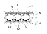
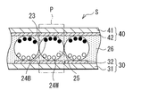
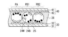
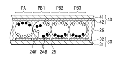
- FIG. 2A and 2B schematically show a configuration example of the display unit 20.
- FIG. 2A shows a case where the pixel P performs white display
- FIG. 2B shows a case where the pixel P performs black display.
- the display unit 20 includes a drive substrate 30, a counter substrate 40, and a plurality of microcapsules 23.
- the drive substrate 30 is disposed on the side opposite to the display surface side in the display unit 20.
- the drive substrate 30 includes a substrate 31 and a plurality of pixel electrodes 32.
- the substrate 31 is formed with a transistor 21, a scanning line SCL, and a signal line SGL.
- the plurality of pixel electrodes 32 are formed on the surface of the substrate 31 at a rate of one for each pixel P.
- the pixel electrode 32 is configured using a metal material such as gold (Au), silver (Ag), copper (Cu), or aluminum (Al).
- the pixel electrode 32 is connected to the drain of the transistor 21. A voltage is supplied to the pixel electrode 32 by the signal line driver 15.
- the counter substrate 40 is disposed on the display surface side of the display unit 20 so as to face the drive substrate 30.
- the counter substrate 40 includes a substrate 41 and a counter electrode 42.
- the substrate 41 is light transmissive.
- the counter electrode 42 is uniformly formed on the surface of the substrate 41 over a region corresponding to the plurality of pixels P.
- the counter electrode 42 is light transmissive and is configured using a light transmissive conductive material such as ITO (Indium Tin Oxide).
- a voltage Vcom (for example, 0 V) is supplied to the counter electrode 42 by the driving unit 10.
- the microcapsule 23 corresponds to the display element 22 and has a spherical shape.
- the microcapsules 23 are arranged between the drive substrate 30 and the counter substrate 40 in a ratio of, for example, a plurality (for example, about four) for each pixel P, and are fixed by a binder 26. 2A and 2B, for convenience of explanation, one microcapsule 23 is drawn for each pixel P.
- a plurality of migrating particles 24W and a plurality of migrating particles 24B are accommodated, and a dispersion medium 25 is filled.
- the migrating particles 24W are responsible for white display and have, for example, positive charges.
- the electrophoretic particle 24B is responsible for black display and has, for example, a negative charge.
- the dispersion medium 25 disperses the plurality of migrating particles 24W and 24B in the microcapsule 23.
- the migrating particles 24W have a positive charge
- the inside of the microcapsule 23 is directed toward the counter electrode 42.
- the migrating particles 24 ⁇ / b> B have a negative charge
- the migrating particles 24 ⁇ / b> B move toward the pixel electrode 32 in the microcapsule 23. Therefore, for example, when the pixel voltage Vpix is set to the voltage Vp for a long time, as shown in FIG. 2A, the migrating particles 24W responsible for white display gather on the display surface S side, so that the pixel P displays white display. Do.
- the migrating particles 24B when the pixel voltage Vpix is set to a negative voltage Vm (for example, ⁇ 15 V), the migrating particles 24B have a negative charge, and thus move in the microcapsule 23 toward the counter electrode 42. Since the migrating particles 24W have a positive charge, they move in the microcapsule 23 toward the pixel electrode 32. Therefore, for example, when the pixel voltage Vpix is set to the voltage Vm for a long time, as shown in FIG. 2B, since the migrating particles 24B responsible for black display gather on the display surface S side, the pixel P displays black display. Do.
- Vm for example, ⁇ 15 V
- the pixel P can perform intermediate gradation display between black display and white display. Further, for example, when the pixel voltage Vpix is the same voltage (for example, 0 V) as the voltage Vcom, the migrating particles 24W and 24B do not move, so that the pixel P can maintain the display state. .
- the migrating particles 24W are responsible for white display and the migrating particles 24B are responsible for black display.
- the present invention is not limited to this, and the migrating particles 24W are responsible for bright display. Any color may be used as long as it is responsible for dark display.
- the migrating particle 24W has a positive charge and the migrating particle 24B has a negative charge.
- the present invention is not limited to this.
- the migrating particle 24B May have a positive charge, and the migrating particles 24W may have a negative charge.
- the pixel P when the pixel voltage Vpix of the pixel P is set to the positive voltage Vp, the pixel P performs black display, the pixel voltage Vpix of the pixel P displays negative voltage Vm, and the pixel P displays white display. Do.
- the drive unit 10 (FIG. 1) drives the display unit 20.
- a temperature sensor 11, a storage unit 12, a processing unit 13, a scanning line driving unit 14, and a signal line driving unit 15 are included.
- the temperature sensor 11 detects the temperature of the display unit 20.
- the storage unit 12 is configured using, for example, a non-volatile memory, and stores image data Dpic, peripheral area information IRB, a plurality of parameter sets PS1, and a plurality of parameter sets PS2.
- the image data Dpic includes pixel values for one frame.
- the peripheral area information IRB is information about the coordinates of the pixels P belonging to the peripheral areas RB1 and RB2 (described later).
- the parameter set PS1 includes a set value for generating a signal to be supplied to the pixel P belonging to the peripheral region RB1.
- a plurality of parameter sets PS1 are stored so that different signals can be generated according to the temperature.
- the parameter set PS2 includes a set value for generating a signal to be supplied to the pixel P belonging to the peripheral region RB2.
- a plurality of parameter sets PS2 are stored so that different signals can be generated according to the temperature.
- the processing unit 13 performs predetermined signal processing based on the image signal Spic supplied from the outside. Specifically, the processing unit 13 causes the storage unit 12 to store pixel values (image data Dpic) for one frame included in the image signal Spic. Then, the processing unit 13 displays the image on the display unit 20 by controlling the scanning line driving unit 14 and the signal line driving unit 15 based on the image data Dpic. Further, the processing unit 13 detects a pixel region RA that performs black display or intermediate gradation display (that is, display other than white display) based on the image data Dpic, and also includes a peripheral region RB1 of the pixel region RA, It also has a function of detecting the peripheral region RB2 outside the peripheral region RB1.
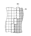
- FIG. 3A shows a detection example of the peripheral region RB1
- FIG. 3B shows a detection example of the peripheral region RB2.
- shaded portions indicate pixel regions RA that perform display other than white display, and portions that are not shaded indicate pixel regions that perform white display.
- the processing unit 13 first detects a pixel region RA that performs display other than white display based on the pixel value of each pixel P included in the image data Dpic. Then, the processing unit 13 detects the peripheral region RB1 of the pixel region RA by performing edge detection processing (FIG. 3A). Further, the processing unit 13 detects a peripheral region RB2 outside the peripheral region RB1 (FIG. 3B).
- the processing unit 13 detects the pixel area RA and the peripheral areas RB1 and RB2 based on the image data Dpic.
- the processing unit 13 stores information on the coordinates of the pixels P belonging to the peripheral regions RB1 and RB2 in the storage unit 12 as peripheral region information IRB.
- the processing unit 13 performs a drawing process on the display unit 20 based on the image data Dpic and the detection result of the temperature sensor 11. At that time, the processing unit 13 performs drawing in the peripheral areas RB1 and RB2 based on the peripheral area information IRB generated based on the previous image data Dpic. Specifically, the processing unit 13 selects one of a plurality of parameter sets PS1 stored in the storage unit 12 based on the detection result in the temperature sensor 11, and based on the selected parameter set PS1. Thus, the signal line driver 15 is controlled so as to generate a signal to be supplied to the pixel P belonging to the peripheral region RB1.
- the processing unit 13 selects one of a plurality of parameter sets PS2 stored in the storage unit 12 based on the detection result in the temperature sensor 11, and based on the selected parameter set PS2,
- the signal line driver 15 is controlled so as to generate a signal to be supplied to the pixel P belonging to the peripheral region RB2.
- the processing unit 13 may be configured by, for example, hardware or a processor that can execute a program.
- the scanning line driving unit 14 sequentially selects the pixels P in units of rows by applying the scanning signal Sc to the plurality of scanning lines SCL based on the signal supplied from the processing unit 13.
- the signal line drive unit 15 generates a signal Sig including three voltages Vp, Vm, and Vcom based on the signal supplied from the processing unit 13. Then, the signal line driver 15 applies this signal Sig to each signal line SGL. Thereby, in the pixel P selected by the scanning line driving unit 14, the voltage (pixel voltage Vpix) of the pixel electrode 32 is set based on the signal Sig.
- peripheral region RB1 corresponds to a specific example of “first peripheral region” in the present disclosure.
- peripheral region RB2 corresponds to a specific example of “second peripheral region” in the present disclosure.
- the temperature sensor 11 detects the temperature of the display unit 20.
- the storage unit 12 stores image data Dpic, peripheral area information IRB, a plurality of parameter sets PS1, and a plurality of parameter sets PS2.
- the processing unit 13 performs predetermined signal processing based on the image signal Spic. Specifically, the processing unit 13 causes the storage unit 12 to store pixel values for one frame included in the image signal Spic as image data Dpic. Then, the processing unit 13 displays the image on the display unit 20 by controlling the scanning line driving unit 14 and the signal line driving unit 15 based on the image data Dpic.
- the processing unit 13 detects a pixel area RA that performs display other than white display, such as black display, based on the image data Dpic, and the peripheral area RB1 of the pixel area RA and the outside of the peripheral area RB1. And the information about the coordinates of the pixels P belonging to the peripheral regions RB1 and RB2 is stored in the storage unit 12 as the peripheral region information IRB. Then, the processing unit 13 performs a drawing process on the display unit 20 based on the image data Dpic and the detection result in the temperature sensor 11. At that time, the processing unit 13 performs drawing in the peripheral areas RB1 and RB2 based on the peripheral area information IRB generated based on the previous image data Dpic.
- the processing unit 13 selects one of a plurality of parameter sets PS1 stored in the storage unit 12 based on the detection result in the temperature sensor 11, and based on the selected parameter set PS1.
- the signal line driver 15 is controlled so as to generate a signal to be supplied to the pixel P belonging to the peripheral region RB1.
- the processing unit 13 selects one of a plurality of parameter sets PS2 stored in the storage unit 12 based on the detection result in the temperature sensor 11, and based on the selected parameter set PS2,
- the signal line driver 15 is controlled so as to generate a signal to be supplied to the pixel P belonging to the peripheral region RB2.
- the scanning line driving unit 14 sequentially selects the pixels P in units of rows by applying the scanning signal Sc to the plurality of scanning lines SCL based on the signal supplied from the processing unit 13.
- the signal line driving unit 15 generates a signal Sig including three voltages Vp, Vm, and Vcom based on the signal supplied from the processing unit 13, and applies the signal Sig to each signal line SGL.
- the display unit 20 displays an image based on driving by the driving unit 10.
- FIG. 4A shows an operation example of the display device 1 when the display state changes from black display to white display.
- FIG. 4A shows waveforms of the scanning signals Sc (1) to Sc (N).
- (B) shows pixel voltages Vpix (1) to Vpix (N) in the pixels P (1) to P (N), and
- (C) shows display states of the pixels P (1) to P (N).
- the pixel P (1) is one of the plurality of pixels P in the first first row in the display unit 20
- the pixel P (N) is the last Nth row in the display unit 20.
- the scanning signal Sc (1) is the scanning signal Sc applied to the scanning line SCL (1) corresponding to the pixel P (1), and the scanning signal Sc (N) is applied to the pixel P (N). This is the scanning signal Sc applied to the corresponding scanning line SCL (N).
- the drawing process is performed on the display unit 20 in the period from the timing t1 to t9 (the drawing period PW), and the pixel voltage Vpix of each pixel P is sequentially set to the negative voltage Vm. This operation will be described in detail below.
- the scanning line driving unit 14 applies scanning signals Sc (1) to Sc (N) to the scanning lines SCL (1) to SCL (N).
- the pixels P are sequentially selected in units of rows (FIG. 4A (A)).
- the scanning signal Sc (1) becomes high level.
- the transistor 21 of the pixel P (1) is turned on, and the pixel voltage Vpix (1) of the pixel P (1) is set to the voltage of the signal Sig (in this example, the voltage Vp) (FIG. 4A (B )).
- the scanning signal Sc (1) changes from the high level to the low level.
- the transistor 21 of the pixel P (1) is turned off.
- the pixel electrode 32 of the pixel P (1) enters a floating state, and the pixel voltage Vpix (1) is maintained at the voltage Vp thereafter.
- the display state in the pixel P (1) starts to change from black display to white display (FIG. 4A (C)).
- the pixel voltages Vpix (2) to Vpix (N) of the pixels P (2) to P (N) are sequentially set to the voltage Vp during the period from the timing t1 to t3 (frame period 1F) (FIG. 4A (B)). Then, the display state in the pixels P (2) to P (N) starts to change sequentially from black display to white display (FIG. 4A (C)).
- the display device 1 operates in the same manner over a plurality of frame periods 1F. Accordingly, the pixel voltages Vpix (1) to Vpix (N) of the pixels P (1) to P (N) are maintained at the voltage Vp, respectively (FIG. 4A (B)), and the pixels P (1) to P (N) ) Continues to change toward white display (FIG. 4A (C)). As a result, at the timing t7, the pixels P (1) to P (N) display white.
- the scanning line driving unit 14 applies the scanning signals Sc (1) to Sc (N) to the scanning lines SCL (1) to SCL (N).
- the pixels P are sequentially selected in units of rows (FIG. 4A (A)).
- the scanning signal Sc (1) becomes high level. Thereby, the transistor 21 of the pixel P (1) is turned on, and the pixel voltage Vpix (1) of the pixel P (1) is set to the voltage of the signal Sig (in this example, the voltage Vcom) (FIG. 4A (B )).
- the scanning signal Sc (1) changes from the high level to the low level. Accordingly, the transistor 21 of the pixel P (1) is turned off.
- the pixel electrode 32 of the pixel P (1) enters a floating state, and the pixel voltage Vpix (1) is maintained at the voltage Vcom thereafter.
- the display state in the pixel P (1) is thereafter maintained as white display (FIG. 4A (C)).
- the pixel voltages Vpix (2) to Vpix (N) of the pixels P (2) to P (N) are sequentially set to the voltage Vcom during the period from the timing t7 to t8 (horizontal period 1H) (FIG. 4A (B)).
- the display state in the pixels P (2) to P (N) is maintained as white display (FIG. 4A (C)).
- FIG. 4B shows an operation example of the display device 1 when the display state changes from white display to black display.
- A shows the waveforms of the scanning signals Sc (1) to Sc (N).
- B shows pixel voltages Vpix (1) to Vpix (N) in the pixels P (1) to P (N), and
- C shows display states of the pixels P (1) to P (N).
- the scanning line driving unit 14 applies scanning signals Sc (1) to Sc (N) to the scanning lines SCL (1) to SCL (N).
- the pixels P are sequentially selected in units of rows (FIG. 4B (A)).
- the pixel voltages Vpix (1) to Vpix (N) of the pixels P (1) to P (N) are sequentially set to the voltage Vm in the period from the timing t1 to t3 (frame period 1F) (FIG. 4B (B)).
- the display states in the pixels P (1) to P (N) start to change sequentially from white display to black display (FIG. 4B (C)).
- the display device 1 operates in the same manner over a plurality of frame periods 1F. Accordingly, the pixel voltages Vpix (1) to Vpix (N) of the pixels P (1) to P (N) are maintained at the voltage Vm (FIG. 4B (B)), and the pixels P (1) to P (N) ) Continues to change toward black display (FIG. 4B (C)). As a result, at the timing t7, the pixels P (1) to P (N) display black.
- the scanning line driving unit 14 applies the scanning signals Sc (1) to Sc (N) to the scanning lines SCL (1) to SCL (N).
- the pixels P are sequentially selected in units of rows (FIG. 4B (A)).
- the pixel voltages Vpix (1) to Vpix (N) of the pixels P (1) to P (N) are sequentially set to the voltage Vcom during the period from the timing t7 to t9 (frame period 1F) (FIG. 4B (B)).
- the display state in the pixels P (1) to P (N) is maintained in black display (FIG. 4B (C)).
- the display device 1 performs the drawing process in the drawing period PW including the plurality of frame periods 1F.
- the display state of all the pixels P of the display device 1 is changed.
- the display state of the pixels P related to the part of the image is changed and the display state of the other pixels P is maintained.
- the display apparatus 1 can suppress the flicker of the display image compared with the case where the display state of all the pixels P is reset.
- edge ghost As described above, when only the pixel P that changes the display state is partially rewritten, there is a possibility that a so-called edge ghost may occur as described below.
- two reference examples E1 and E2 in which an edge ghost can occur will be described.
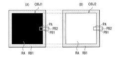
- FIG. 5 shows a display image according to Reference Example E1
- (A) shows a display example when a square black object OBJ1 is displayed
- (B) shows this black object OBJ1 as a white object OBJ2.
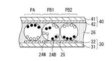
- FIG. 6A shows the states of the pixels PA, PB1, and PB2 in FIG.
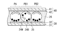
- FIG. 6B shows the state of the pixels PA, PB1, and PB2 in FIG.
- the pixel PA is a pixel P belonging to the pixel area RA displaying the object OBJ1
- the pixel PB1 is a pixel P belonging to the peripheral area RB1 of the pixel area RA
- the pixel PB2 is a peripheral area outside the peripheral area RB1. This is a pixel P belonging to RB2.
- the display unit 20 performs white display over the entire screen
- the pixel voltage Vpix of the pixel P belonging to RA is set to a negative voltage Vm.
- the pixel voltage Vpix of the pixels P belonging to the peripheral regions RB1 and RB2 are both set to the voltage Vcom in this example.
- the pixel PA can perform black display.
- part of the electric field generated by the pixel PA also enters the pixel P in the vicinity of the pixel PA, and the migrating particles 24B and 24W may move in the pixel P in the vicinity according to the electric field.
- this pixel PB1 performs gray display, for example.
- a gray ring is displayed around the object OBJ1.
- the pixel voltage Vpix of the pixel PA belonging to the pixel area RA is positive.
- the voltage Vp is set.
- the pixel voltages Vpix of the pixels PB1 and PB2 belonging to the peripheral regions RB1 and RB2 are both set to the voltage Vcom in this example.
- the pixel PA can perform white display.
- some of the migrating particles 24B do not return near the pixel electrode 32, and some of the migrating particles 24W do not return near the counter electrode 42.
- a gray ring remains around the object OBJ2. That is, by rewriting the black object OBJ1 to the white object OBJ2, it is expected that the display unit 20 performs white display over the entire surface, but in this example, a gray ring is displayed as an edge ghost.
- FIG. 7 shows a display image according to Reference Example E2, (A) shows a display example when a square black object OBJ1 is displayed, and (B) shows this black object OBJ1 as a white object OBJ2. An example of display when rewritten is shown.
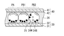
- FIG. 8A shows the states of the pixels PA, PB1, and PB2 in FIG.
- FIG. 8B shows the state of the pixels PA, PB1, and PB2 in FIG. 7B.
- the pixel voltage Vpix of the pixel P belonging to the pixel area RA is set to the negative voltage Vm, and the pixel voltage of the pixel P belonging to the peripheral areas RB1 and RB2 is set. Both Vpix are set to the voltage Vcom.
- a gray ring is displayed around the object OBJ1.
- the pixel voltage Vpix of the pixel P belonging to the pixel area RA is a positive voltage.
- the pixel voltage Vpix of the pixel P belonging to the peripheral region RB1 is set to the voltage Vp for a short time.
- the pixel voltage Vpix of the pixel P belonging to the peripheral region RB2 is set to the voltage Vcom.
- the pixels PA and PB1 can perform white display.
- a part of the electric field generated by the pixel PB1 also enters the pixel P in the vicinity of the pixel PA, and the migrating particles 24B and 24W may move in the pixel P in the vicinity according to the electric field.
- the migrating particles 24B and 24W may move in the pixel P in the vicinity according to the electric field.
- this pixel PB2 performs gray display, for example.
- a gray ring is displayed as an edge ghost.
- Such a phenomenon becomes prominent when the microcapsule 23 having a high moving speed of the migrating particles 24B and 24W is used. That is, when rewriting an image in a short time, it is desirable to increase the moving speed of the migrating particles 24B and 24W, but in that case, there is a possibility that the edge coast is likely to occur in this way.
- the pixel voltage Vpix of the pixel P belonging to the peripheral region RB1 is set to the voltage Vp for a short time, for example, and the pixel voltage Vpix of the pixel P belonging to the peripheral region RB2 is set to, for example, Further, the voltage Vp is set for a short time.
- FIG. 9 shows a display image according to the present embodiment, where FIG. 9A shows a display example when a square black object OBJ1 is displayed, and FIG. 9B shows the black object OBJ1 as a white object OBJ2. Shows a display example when rewritten.
- FIG. 10A shows the states of the pixels PA, PB1, and PB2 in FIG.
- FIG. 10B shows the state of the pixels PA, PB1, and PB2 in FIG. 9B.
- the driving unit 10 sets the pixel voltage Vpix of the pixel P belonging to the pixel region RA to the negative voltage Vm, and the pixels of the pixel P belonging to the peripheral regions RB1 and RB2 Both voltages Vpix are set to voltage Vcom. As a result, as shown in FIGS. 9A and 10A, a gray ring is displayed around the object OBJ1.
- the driving unit 10 sets the pixel voltage Vpix of the pixel P belonging to the pixel region RA to the positive voltage Vp.
- the driving unit 10 sets the pixel voltage Vpix of the pixel P belonging to the peripheral region RB1 to the voltage Vp for a short time, for example, and sets the pixel voltage Vpix of the pixel P belonging to the peripheral region RB2 to a voltage for a shorter time, for example. Set to Vp.
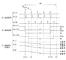
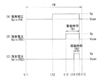
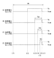
- FIG. 11 shows an example of the waveform of the pixel voltage Vpix.
- A shows the waveform of the pixel voltage Vpix (PA) of the pixel PA
- B shows the waveform of the pixel voltage Vpix (PB1) of the pixel PB1.
- C shows the waveform of the pixel voltage Vpix (PB2) of the pixel PB2.
- the drive unit 10 performs a drawing process on the display unit 20 during the period from the timing t11 to t16 (the drawing period PW). Specifically, first, at timing t12, the driving unit 10 sets the pixel voltage Vpix (PA) of the pixel PA to the positive voltage Vp (FIG. 11A).
- the drive unit 10 sets the pixel voltage Vpix (PB1) of the pixel PB1 to the positive voltage Vp (FIG. 11B). Then, at the timing t14, the drive unit 10 sets the pixel voltage Vpix (PB2) of the pixel PB2 to the positive voltage Vp (FIG. 11C). At timing t15, the drive unit 10 sets the pixel voltages Vpix (PA), Vpix (PB1), and Vpix (PB2) to the voltage Vcom (FIGS. 11A to 11C).
- the pixel voltage Vpix (PB1) of the pixel PB1 corresponds to a specific example of “first pulse signal” in the present disclosure.
- the pixel voltage Vpix (PB2) of the pixel PB2 corresponds to a specific example of “second pulse signal” in the present disclosure.
- the pixel voltage Vpix (PA) of the pixel PA corresponds to a specific example of “fourth pulse signal” in the present disclosure.
- the driving unit 10 sets the pixel voltage Vpix of the pixel P belonging to the peripheral region RB1 to the voltage Vp for a short time, and sets the pixel voltage Vpix of the pixel P belonging to the peripheral region RB2 to the voltage Vp for a further short time.
- the possibility that the pixels PB1 and PB2 perform gray display can be reduced, so that an edge ghost occurs as shown in FIG. 9B. The fear can be reduced.
- the black object OBJ1 is displayed.
- the present invention is not limited to this, and the intermediate-tone object OBJ1 may be displayed.
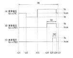
- FIG. 12 shows an example of the waveform of the pixel voltage Vpix when the white object OBJ2 is displayed after the half-tone object OBJ1 is displayed.
- FIG. 12A shows the pixel voltage Vpix (PA) of the pixel PA.
- (B) shows the waveform of the pixel voltage Vpix (PB1) of the pixel PB1, and (C) shows the waveform of the pixel voltage Vpix (PB2) of the pixel PB2.
- the drive unit 10 performs a drawing process on the display unit 20 during the period from the timing t21 to t27 (the drawing period PW).
- the driving unit 10 sets the pixel voltage Vpix (PA) of the pixel PA to the negative voltage Vm at the timing t22, and sets the pixel voltage Vpix (PA) to the positive voltage Vp at the timing t23.
- This is set (FIG. 12A). That is, in this example, in order to display the white object OBJ2 after displaying the half-tone object OBJ1, the display state of the pixel PA is once displayed in black and then displayed in white.
- the driving unit 10 sets the pixel voltage Vpix (PB1) to the positive voltage Vp at timing t24 (FIG. 12B), and sets the pixel voltage Vpix (PB2) to the positive voltage Vp at timing t25. (FIG. 12C).
- the drive unit 10 sets the pixel voltages Vpix (PA), Vpix (PB1), and Vpix (PB2) to the voltage Vcom (FIGS. 12A to 12C).
- the possibility that the pixels PB1 and PB2 perform gray display can be reduced, so that the possibility that an edge ghost is generated can be reduced.
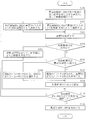
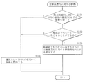
- FIG. 13 shows an operation example of the drive unit 10.
- the drive unit 10 performs a drawing process on the display unit 20 based on the received image data Dpic. At that time, the drive unit 10 performs drawing in the peripheral regions RB1 and RB2 based on the peripheral region information IRB generated based on the previous image data Dpic. This operation will be described in detail below.
- the driving unit 10 starts driving the pixels P that change the display state in the regions other than the peripheral regions RB1 and RB2 based on the image data Dpic (step S101). ).
- the processing unit 13 first receives the image data Dpic, the processing unit 13 stores the image data Dpic in the storage unit 12. Further, the processing unit 13 specifies the peripheral regions RB1 and RB2 based on the peripheral region information IRB stored in the storage unit 12. Then, the drive unit 10 starts driving the pixels P that change the display state in the regions other than the peripheral regions RB1 and RB2 based on the image data Dpic.
- the processing unit 13 selects one of the pixels P belonging to the peripheral regions RB1 and RB2 as the target pixel PZ to be processed (step S102).
- the processing unit 13 acquires the temperature T of the display unit 20 based on the detection result in the temperature sensor 11 (step S103).
- the processing unit 13 confirms whether or not the pixel value in the target pixel PZ indicates white display based on the image data Dpic (step S104).
- the drive unit 10 determines the target pixel PZ according to the pixel value. Driving is started (step S105), and the process proceeds to step S110.
- step S104 when the pixel value in the target pixel PZ indicates white display (“Y” in step S104), the processing unit 13 determines whether the target pixel PZ is a pixel belonging to the peripheral region RB1. (Step S106). When the target pixel PZ is a pixel belonging to the peripheral region RB1 (“Y” in step S106), the processing unit 13 uses a plurality of parameters stored in the storage unit 12 based on the temperature T acquired in step S103. A parameter set PS1 corresponding to the temperature T is selected from the set PS1 (step S107).
- the processing unit 13 stores a plurality of data stored in the storage unit 12 based on the temperature T acquired in step S103.
- the parameter set PS2 corresponding to the temperature T is selected from the parameter set PS2 (step S108).
- the driving unit 10 drives the target pixel PZ (step S109).
- FIG. 14 shows a driving operation for the target pixel PZ.
- the processing unit 13 confirms whether or not the driving for the pixels P in the regions other than the peripheral regions RB1 and RB2 that have started driving in step S101 has already been completed (step S121). Specifically, for example, in the example of FIG. 11, when the timing at which this processing is performed is before the timing t12, the processing unit 13 has not yet started driving the pixel PA, and the timing t12. If it is within the period of t15, the pixel PA is driven. Therefore, when the timing at which this processing is performed is before the timing t15, the processing unit 13 determines that the driving for the pixel PA has not been finished yet.
- the processing unit 13 determines that the driving for the pixel PA has already been completed. In this way, the processing unit 13 confirms whether or not driving for the pixels P in the regions other than the peripheral regions RB1 and RB2 has already been completed. If the driving has already been completed ("Y" in step S121), the process proceeds to step S124.
- step S121 when the driving has not been finished yet ("N" in step S121), the processing unit 13 drives the driving for the pixel P in the region other than the peripheral regions RB1 and RB2 and the driving for the target pixel PZ. It is confirmed whether or not the end timing can be matched (step S122). Specifically, the processing unit 13 first obtains the drive time for the target pixel PZ based on the parameter set selected in steps S108 and S109. Specifically, for example, in the example of FIG. 11, when the target pixel PZ is the pixel PB1, the processing unit 13 determines the drive time TB1 (timing t13) based on the parameter set selected in steps S108 and S109. (Time length of the period of t15).
- the processing unit 13 performs pixel P () in the region other than the peripheral regions RB1 and RB2. For example, it is determined that the drive end timing for the pixel PA) and the drive end timing for the target pixel PZ (for example, the pixel PB1) can be matched.
- the processing unit 13 performs a driving end timing for the pixel P (for example, the pixel PA) in a region other than the peripheral regions RB1 and RB2.
- step S122 If the drive end timing cannot be matched ("N" in step S122), the process proceeds to step S124.
- step S122 If the drive end timing can be matched in step S122 (“Y” in step S122), the processing unit 13 sets the drive start timing for the target pixel PZ so that the drive end timing is matched. (Step S123). Thereby, the drive part 10 starts the drive with respect to this object pixel PZ when it becomes this drive start timing after that.
- step S121 when the driving has already been completed in step S121 (“Y” in step S121), or when the driving end timing cannot be matched in step S122 (“N” in step S122), the driving is performed.
- the unit 10 immediately starts driving the target pixel PZ based on the parameter set selected in steps S108 and S109 (step S124).
- the drive end timing for the target pixel PZ is later than the drive end timing for the pixels P in the regions other than the peripheral regions RB1 and RB2, but even in this case, the possibility of occurrence of edge ghost may be reduced. it can. Then, this subroutine ends.
- the processing unit 13 confirms whether or not all the pixels P belonging to the peripheral regions RB1 and RB2 have been selected (step S110). If all the pixels P have not been selected (“N” in step S110), the processing unit 13 targets one of the unselected pixels P among the pixels P belonging to the peripheral regions RB1 and RB2. The pixel PZ is selected (step S111), and the process proceeds to step S103. Steps S103 to S111 are repeated until all the pixels P are selected.
- the processing unit 13 detects the peripheral regions RB1 and RB2 based on the image data Dpic (step S112). Then, the processing unit 13 generates peripheral area information IRB based on the detection result, and stores the peripheral area information IRB in the storage unit 12.
- the pixels P belonging to the peripheral region RB2 are also driven.
- the possibility that the pixels PB1 and PB2 may perform gray display can be reduced, so that the possibility that an edge ghost is generated can be reduced.
- the image quality can be improved.
- the drive time TB2 for the pixel P (for example, the pixel PB2) belonging to the peripheral region RB2 is changed to the drive time TB2 for the pixel P (for example, the pixel PB1) belonging to the peripheral region RB1. Since it is shorter than TB1, the image quality can be improved. That is, for example, when the drive time TB2 is the same as the drive time TB1, an edge ghost may occur in the peripheral region outside the peripheral region RB2.
- the drive time TB2 since the drive time TB2 is shorter than the drive time TB1, the influence of the electric field generated by the pixel P belonging to the peripheral region RB2 on the pixels P outside the peripheral region RB2 can be reduced. Therefore, the possibility that an edge ghost is generated in the peripheral region outside the peripheral region RB2 can be reduced. As a result, the display device 1 can improve the image quality.
- the drive end timing for the pixels P (for example, the pixel PA) other than the peripheral regions RB1 and RB2, and the pixels P (for example, the pixels P belonging to the peripheral regions RB1 and RB2) Since the drive end timings for the pixels PB1 and PB2) are made to coincide with each other, the image quality can be improved. That is, for example, when the driving end timing for the pixels PB1 and PB2 is made earlier than the driving end timing for the pixel PA, the electric field generated by the pixel PA is applied to the pixel PB1 after the driving for the pixels PB1 and PB2 is completed. There is a risk that edge ghosting may occur.
- the display device 1 since the drive end timing for the pixel PA and the drive end timing for the pixels PB1 and PB2 are made to coincide with each other, the possibility of the occurrence of edge ghost can be reduced. As a result, the display device 1 can improve the image quality.
- the drive unit 10 selects a parameter set PS1 corresponding to the temperature T from the plurality of parameter sets PS1, and supplies signals to the pixels P belonging to the peripheral region RB1 based on the parameter set PS1.
- the driving unit 10 selects a parameter set PS2 corresponding to the temperature T from the plurality of parameter sets PS2, and generates a signal to be supplied to the pixels P belonging to the peripheral region RB2 based on the parameter set PS2.
- an image quality can be improved. That is, the characteristics of the display unit 20 can be changed by the temperature T. Therefore, it is desirable to change the drive times TB1, TB2 and the like according to the temperature T.
- the display device 1 Since the display device 1 generates a signal to be supplied to the pixels P belonging to the peripheral regions RB1 and RB2 based on the temperature T, it is possible to reduce the possibility that an edge ghost is effectively generated at various temperatures. As a result, the image quality can be improved.
- the display device 1 performs drawing in the peripheral areas RB1 and RB2 based on the peripheral area information IRB generated based on the previous image data Dpic. Thereby, for example, the amount of calculation performed when new image data Dpic is supplied can be reduced. As a result, the display device 1 can shorten the time from the supply of the image data Dpic to the end of drawing.
- the drive time for the pixels belonging to the peripheral region RB2 is shorter than the drive time for the pixels belonging to the peripheral region RB1, so that the image quality can be improved.
- the drive end timing for the pixels in the regions other than the peripheral regions RB1 and RB2 and the drive end timing for the pixels belonging to the peripheral regions RB1 and RB2 are matched, so that the image quality can be improved.
- the image quality can be improved.
- the drawing in the peripheral areas RB1 and RB2 is performed based on the peripheral area information generated based on the previous image data, the drawing is completed after the image data is supplied.
- the time can be shortened.
- the pixel voltage Vpix of the pixels P belonging to the peripheral regions RB1 and RB2 is set to the positive voltage Vp.
- the present invention is not limited to this. Instead, the pixel voltage Vpix may be set to the negative voltage Vm before the pixel voltage Vpix is set to the positive voltage Vp, for example, as in the display device 1A shown in FIG.
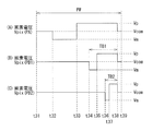
- the drive unit 10A of the display device 1A performs the drawing process on the display unit 20 during the period from the timing t31 to t39 (the drawing period PW).
- the driving unit 10A sets the pixel voltage Vpix (PA) of the pixel PA to the negative voltage Vm at the timing t32, and sets the pixel voltage Vpix (PA) to the positive voltage Vp at the timing t33.
- the setting is made (FIG. 15A).
- the driving unit 10A sets the pixel voltage Vpix (PB1) of the pixel PB1 to the negative voltage Vm at the timing t34, and sets the pixel voltage Vpix (PB1) to the positive at the timing t35.
- the voltage Vp is set (FIG. 15B).
- the driving unit 10A sets the pixel voltage Vpix (PB2) of the pixel PB2 to the negative voltage Vm at the timing t36, and sets the pixel voltage Vpix (PB2) to the positive at the timing t37.
- the voltage Vp is set (FIG. 15C).
- the driving unit 10A sets the pixel voltages Vpix (PA), Vpix (PB1), and Vpix (PB2) to the voltage Vcom (FIGS. 15A to 15C).
- the drive time TB2 for the pixel P belonging to the peripheral region RB2 is shorter than the drive time TB1 for the pixel P belonging to the peripheral region RB1, but the present invention is not limited to this.
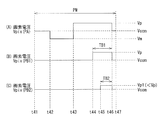
- the pixel voltage Vpix of the pixel P belonging to the peripheral region RB2 may be made lower than the pixel voltage Vpix of the pixel P belonging to the peripheral region RB1, as in the display device 1B shown in FIG.
- the drive unit 10B of the display device 1B performs the drawing process on the display unit 20 during the period from the timing t41 to t47 (the drawing period PW).
- the driving unit 10B sets the pixel voltage Vpix (PA) of the pixel PA to the negative voltage Vm at the timing t42, and sets the pixel voltage Vpix (PA) to the positive voltage Vp at the timing t43. This is set (FIG. 16A).
- the driving unit 10B sets the pixel voltage Vpix (PB1) of the pixel PB1 to the positive voltage Vp at the timing t44 (FIG. 16B).
- the driving unit 10B sets the pixel voltage Vpix (PB2) of the pixel PB2 to the positive voltage Vp1 at the timing t45 (FIG. 16C). This voltage Vp1 is lower than the voltage Vp (Vp1 ⁇ Vp).
- the drive unit 10B sets the pixel voltages Vpix (PA), Vpix (PB1), and Vpix (PB2) to the voltage Vcom (FIGS. 16A to 16C).
- the present modification is applied to the display device 1 according to the above-described embodiment (for example, FIG. 12).
- An example may apply.
- the pixel voltage Vpix of the pixels P belonging to the peripheral regions RB1 and RB2 is set to the voltage Vp.
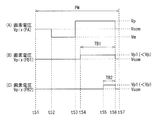
- the present invention is not limited to this. Instead, the pixel voltage Vpix of the pixels P belonging to the peripheral regions RB1 and RB2 may be set to a positive voltage Vp1 lower than the voltage Vp, for example, as in the display device 1C shown in FIG.
- the drive unit 10C of the display device 1C performs the drawing process on the display unit 20 during the period from the timing t51 to the time t57 (the drawing period PW).
- the driving unit 10C sets the pixel voltage Vpix (PA) of the pixel PA to the negative voltage Vm at the timing t52, and sets the pixel voltage Vpix (PA) to the positive voltage Vp at the timing t53. This is set (FIG. 17A). Further, the driving unit 10C sets the pixel voltage Vpix (PB1) of the pixel PB1 to the positive voltage Vp1 at the timing t54 (FIG. 17B), and the pixel voltage Vpix (PB2) of the pixel PB2 at the timing t55. The positive voltage Vp1 is set (FIG. 17C). At timing t56, the drive unit 10C sets the pixel voltages Vpix (PA), Vpix (PB1), and Vpix (PB2) to the voltage Vcom (FIGS. 17A to 17C).
- the pixel voltage Vpix of the pixels P belonging to the peripheral regions RB1 and RB2 may be set to the voltage Vp1 in a plurality of times. As a result, the risk of edge ghosts occurring in the peripheral region outside the peripheral region RB1 can be reduced.
- the pixels P belonging to the peripheral regions RB1 and RB2 are driven.
- the present invention is not limited to this, and the pixels P in one or more peripheral regions on the outer side may also be driven.
- the display device 1D according to the present modification will be described in detail.
- FIG. 19 shows a display image according to this modification.
- FIG. 19A shows a display example when a square black object OBJ1 is displayed, and
- FIG. 19B shows this black object OBJ1 as a white object OBJ2.
- FIG. 20A shows the states of the pixels PA, PB1, PB2, and PB3 in FIG.
- FIG. 20B shows the states of the pixels PA, PB1, PB2, and PB3 in FIG.
- the pixel PB3 is a pixel P that belongs to the peripheral region RB3 outside the peripheral region RB2.
- the driving unit 10D of the display device 1D sets the pixel voltage Vpix of the pixel P belonging to the pixel region RA to the negative voltage Vm, and the peripheral regions RB1, RB2, RB3.
- the pixel voltage Vpix of the pixel P belonging to is set to the voltage Vcom.
- FIGS. 19A and 20A a gray ring is displayed around the object OBJ1.
- the driving unit 10D sets the pixel voltage Vpix of the pixel P belonging to the pixel region RA to the positive voltage Vp. At that time, the driving unit 10D applies the voltage Vp to the pixels P belonging to the peripheral regions RB1, RB2, and RB3 for a short time.
- FIG. 21 shows an example of the waveform of the pixel voltage Vpix.
- A shows the waveform of the pixel voltage Vpix (PA) of the pixel PA
- B shows the waveform of the pixel voltage Vpix (PB1) of the pixel PB1.
- C shows the waveform of the pixel voltage Vpix (PB2) of the pixel PB2, and
- D shows the waveform of the pixel voltage Vpix (PB3) of the pixel PB3.
- the driving unit 10D performs the drawing process on the display unit 20 during the period from the timing t71 to t77 (the drawing period PW).
- the driving unit 10D sets the pixel voltage Vpix (PA) of the pixel PA to the positive voltage Vp (FIG. 21A).
- the driving unit 10D sets the pixel voltage Vpix (PB1) of the pixel PB1 to the positive voltage Vp (FIG. 21B), and at timing t74, the driving unit 10D sets the pixel voltage Vpix (PB2) of the pixel PB2.
- the positive voltage Vp is set (FIG. 21C), and at the timing t75, the pixel voltage Vpix (PB3) of the pixel PB3 is set to the positive voltage Vp (FIG. 21D).
- the driving unit 10D sets the pixel voltages Vpix (PA), Vpix (PB1), Vpix (PB2), and Vpix (PB3) to the voltage Vcom (FIGS. 21A to 21D).
- the driving unit 10D sets the pixel voltage Vpix of the pixel P belonging to the peripheral region RB1 to the voltage Vp for a short time, and sets the pixel voltage Vpix of the pixel P belonging to the peripheral region RB2 to the voltage Vp for a further short time.
- the pixel voltage Vpix of the pixel P belonging to the peripheral region RB3 is set to the voltage Vp for a shorter time. Accordingly, in the display device 1D, as illustrated in FIG. 20B, for example, the possibility that the pixels PB1, PB2, and PB3 perform gray display can be reduced. Therefore, as illustrated in FIG. The risk of occurrence can be reduced.
- the electronic book includes, for example, a display unit 110, a housing 120, and an operation unit 130.
- the operation unit 130 may be provided on the front surface of the housing 120 as illustrated in FIG. 22A, or may be provided on the side surface of the housing 120 as illustrated in FIG. 22B.
- the display unit 110 is configured by the display device described above.
- the above display device may be mounted on a PDA (Personal Digital Assistants) or the like having the same configuration as the electronic book shown in FIGS. 22A and 22B.
- PDA Personal Digital Assistants
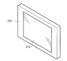
- FIG. 23 shows the appearance of a tablet computer.
- the tablet computer has, for example, a touch panel unit 310 and a housing 320, and the touch panel unit 310 is configured by the display device described above.
- the above display device can be applied as a so-called wearable terminal to a part of clothing such as a watch (watch), bag, clothes, hat, glasses and shoes. Below, an example of such an electronic device integrated with clothing is shown.
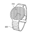
- FIG. 24A and FIG. 24B show the appearance of an electronic timepiece (wristwatch-integrated electronic device).
- This electronic timepiece has, for example, a dial (character information display part) 410 and a band part (color pattern display part) 420, and these dial 410 and band part 420 include the display device described above.
- a dial character information display part
- a band part color pattern display part
- FIGS. 24A and 24B show the appearance of an electronic timepiece (wristwatch-integrated electronic device).
- This electronic timepiece has, for example, a dial (character information display part) 410 and a band part (color pattern display part) 420, and these dial 410 and band part 420 include the display device described above.
- the band unit 420 is a part that can be attached to, for example, an arm.
- various color patterns can be displayed, and the design of the band unit 420 can be changed from the example of FIG. 24A to the example of FIG. 24B. it can. In this way, it is possible to
- the present technology has been described with reference to the embodiment, the modification, and the application example to the electronic device.
- the present technology is not limited to the embodiment and the like, and various modifications are possible.
- the microcapsule type electrophoretic element is used.
- the present invention is not limited to this, and another type electrophoretic element may be used.
- the pixel of the first pixel belonging to the first peripheral region outside the pixel region to be rewritten from the color other than the predetermined color to the predetermined color
- the first pixel is driven so that a first pulse signal is generated in the electrode, and a second pulse is applied to the pixel electrode of the second pixel belonging to the second peripheral region outside the first peripheral region.
- a driving device including a driving unit that drives the second pixel so that a signal is generated.
- the driving unit further controls the third pixel so that a third pulse signal is generated in the pixel electrode of the third pixel belonging to the third peripheral region outside the second peripheral region.
- the drive device according to (1).
- the drive unit A fourth peripheral area outside the pixel area indicating a color other than the predetermined color in the first image data based on the first image data, and a fifth peripheral area outside the fourth peripheral area Detect
- the first peripheral area is obtained based on the pixel value of each pixel belonging to the fourth peripheral area in the second image data next to the first image data, and each belonging to the fifth peripheral area
- the driving unit drives the fourth pixel so that a fourth pulse signal is generated in the pixel electrode of the fourth pixel belonging to the pixel region,
- the drive device according to any one of (1) to (5), wherein an end timing of the first pulse signal is a timing corresponding to an end timing of the fourth pulse signal.
- the driving unit drives the fourth pixel so that a fourth pulse signal is generated in the pixel electrode of the fourth pixel belonging to the pixel region,
- the drive device according to any one of (1) to (7), wherein an end timing of the second pulse signal is a timing corresponding to an end timing of the fourth pulse signal.
- the first pulse signal includes a first voltage corresponding to the predetermined color, a second voltage, and a third voltage between the first voltage and the second voltage.
- the second pulse signal includes a fourth voltage corresponding to the predetermined color, a fifth voltage, and the third voltage.
- the length of the period that is the fourth voltage in the second pulse signal is shorter than the length of the period that is the first voltage in the first pulse signal.
- the first pulse signal includes a first voltage corresponding to the predetermined color, a second voltage, and a third voltage between the first voltage and the second voltage.
- the second pulse signal includes a fourth voltage corresponding to the predetermined color, a fifth voltage, and the third voltage.
- the drive according to any one of (1) to (3), wherein a voltage difference between the fourth voltage and the third voltage is smaller than a voltage difference between the first voltage and the third voltage. apparatus.
- the driving unit drives the fourth pixel so that a fourth pulse signal is generated in the pixel electrode of the fourth pixel belonging to the pixel region,
- the drive device according to any one of (10) to (12), wherein an end timing of the first pulse signal is a timing corresponding to an end timing of the fourth pulse signal.
- the driving unit drives the fourth pixel so that a fourth pulse signal is generated in the pixel electrode of the fourth pixel belonging to the pixel region,
- the drive device according to any one of (10) to (13), wherein an end timing of the second pulse signal is a timing corresponding to an end timing of the fourth pulse signal.
- the driving unit includes: A storage unit that stores a plurality of first parameter sets for generating the first pulse signal and a plurality of second parameter sets for generating the second pulse signal; The first pixel is driven based on any one of the plurality of first parameter sets, and the second pixel is driven based on any one of the plurality of second parameter sets.
- the drive device according to any one of (1) to (14).
- the driving unit includes: A temperature sensor; Based on the detection result in the temperature sensor, one of the plurality of first parameter sets is selected, and one of the plurality of second parameter sets is selected and selected.
- the driving device according to (15), wherein the first pixel is driven based on the set first parameter set, and the second pixel is driven based on the selected second parameter set.
- the pixel of the first pixel belonging to the first peripheral region outside the pixel region to be rewritten from the color other than the predetermined color to the predetermined color
- Driving the first pixel to generate a first pulse signal on the electrode;
- a driving method for driving the second pixel such that a second pulse signal is generated in the pixel electrode of the second pixel belonging to the second peripheral region outside the first peripheral region.
- a display unit having a plurality of pixels each having an electrophoretic element and a pixel electrode; Among the plurality of pixels, the first pulse signal is generated so that a first pulse signal is generated in the pixel electrode of the first pixel belonging to the first peripheral region outside the pixel region to be rewritten from the color other than the predetermined color to the predetermined color.
- a display device comprising a drive unit.
Landscapes
- Engineering & Computer Science (AREA)
- Physics & Mathematics (AREA)
- Computer Hardware Design (AREA)
- General Physics & Mathematics (AREA)
- Theoretical Computer Science (AREA)
- Electrochromic Elements, Electrophoresis, Or Variable Reflection Or Absorption Elements (AREA)
- Control Of Indicators Other Than Cathode Ray Tubes (AREA)
Abstract
本開示の駆動装置は、それぞれが電気泳動素子と画素電極とを有する複数の画素のうち、所定色以外の色から所定色に書き換える画素領域の外側の第1の周辺領域に属する第1の画素の画素電極に第1のパルス信号が生じるように第1の画素を駆動するとともに、第1の周辺領域の外側の第2の周辺領域に属する第2の画素の画素電極に第2のパルス信号が生じるように第2の画素を駆動する駆動部を備える。
Description
本開示は、電気泳動表示素子を用いた表示装置を駆動する駆動装置および駆動方法、ならびにそのような駆動装置を備えた表示装置に関する。
例えば電子ペーパーには、しばしば、電気泳動表示素子を用いた双安定の電子光学ディスプレイが用いられる。例えば、特許文献1,2には、電子光学ディスプレイの駆動方法が開示されている。
ところで、一般に、表示装置では、画質が高いことが望まれており、電気泳動表示素子を用いた電子光学ディスプレイにおいても、画質の向上が期待されている。
画質を高めることができる駆動装置、駆動方法、および表示装置を提供することが望ましい。
本開示の一実施の形態における駆動装置は、駆動部を備えている。駆動部は、それぞれが電気泳動素子と画素電極とを有する複数の画素のうち、所定色以外の色から所定色に書き換える画素領域の外側の第1の周辺領域に属する第1の画素の画素電極に第1のパルス信号が生じるように第1の画素を駆動するとともに、第1の周辺領域の外側の第2の周辺領域に属する第2の画素の画素電極に第2のパルス信号が生じるように第2の画素を駆動するものである。
本開示の一実施の形態における駆動方法は、それぞれが電気泳動素子と画素電極とを有する複数の画素のうち、所定色以外の色から所定色に書き換える画素領域の外側の第1の周辺領域に属する第1の画素の画素電極に第1のパルス信号が生じるように第1の画素を駆動し、第1の周辺領域の外側の第2の周辺領域に属する第2の画素の画素電極に第2のパルス信号が生じるように第2の画素を駆動するものである。
本開示の一実施の形態における表示装置は、表示部と、駆動部とを備えている。表示部は、それぞれが電気泳動素子と画素電極とを有する複数の画素を有するものである。駆動部は、複数の画素のうち、所定色以外の色から所定色に書き換える画素領域の外側の第1の周辺領域に属する第1の画素の画素電極に第1のパルス信号が生じるように第1の画素を駆動するとともに、第1の周辺領域の外側の第2の周辺領域に属する第2の画素の画素電極に第2のパルス信号が生じるように第2の画素を駆動するものである。
本開示の一実施の形態における駆動装置、駆動方法、および表示装置では、画素領域が、所定色以外の色から所定色に書き換えられる。そして、その画素領域の外側の第1の周辺領域に属する第1の画素が、その第1の画素の画素電極に第1のパルス信号が生じるように駆動される。そして、その第1の周辺領域の外側の第2の周辺領域に属する第2の画素が、その第2の画素の画素電極に第2のパルス信号が生じるように駆動される。
本開示の一実施の形態における駆動装置、駆動方法、および表示装置によれば、第1の周辺領域に属する第1の画素の画素電極に第1のパルス信号が生じるように第1の画素を駆動するとともに、第2の周辺領域に属する第2の画素の画素電極に第2のパルス信号が生じるように第2の画素を駆動したので、画質を高めることができる。なお、ここに記載された効果は必ずしも限定されるものではなく、本開示中に記載されたいずれの効果があってもよい。
以下、本開示の実施の形態について、図面を参照して詳細に説明する。なお、説明は以下の順序で行う。
1.実施の形態
2.適用例
1.実施の形態
2.適用例
<1.実施の形態>
[構成例]
図1は、一実施の形態に係る表示装置(表示装置1)の一構成例を表すものである。表示装置1は、電気泳動表示素子を用いた双安定の電子光学ディスプレイである。なお、本開示の実施の形態に係る駆動装置および駆動方法は、本実施の形態により具現化されるので、併せて説明する。表示装置1は、表示部20と、駆動部10とを備えている。
[構成例]
図1は、一実施の形態に係る表示装置(表示装置1)の一構成例を表すものである。表示装置1は、電気泳動表示素子を用いた双安定の電子光学ディスプレイである。なお、本開示の実施の形態に係る駆動装置および駆動方法は、本実施の形態により具現化されるので、併せて説明する。表示装置1は、表示部20と、駆動部10とを備えている。
表示部20は、複数の画素9がマトリックス状に配置されたものである。また、表示部20は、水平方向(図1における横方向)に延伸する複数(この例ではN本)の走査線SCL(走査線SCL(1)~SCL(N))と、垂直方向(図1における縦方向)に延伸する複数の信号線SGLとを有している。複数の走査線SCLの一端、および複数の信号線SGLの一端は、駆動部10にそれぞれ接続されている。
画素Pは、トランジスタ21と、表示素子22とを有している。トランジスタ21は、この例ではN型のMOS(Metal Oxide Semiconductor)トランジスタである。トランジスタ21のソースは信号線SGLに接続され、ゲートは走査線SCLに接続され、ドレインは表示素子22に接続されている。表示素子22は、この例では、マイクロカプセル方式の電気泳動素子を含んで構成されるものであり、一端はトランジスタ21のドレインに接続され、他端には電圧Vcom(例えば0V)が供給されている。
図2A,2Bは、表示部20の一構成例を模式的に表すものであり、図2Aは画素Pが白表示を行う場合を示し、図2Bは画素Pが黒表示を行う場合を示す。表示部20は、駆動基板30と、対向基板40と、複数のマイクロカプセル23とを有している。
駆動基板30は、表示部20における表示面側とは反対側に配置されるものである。駆動基板30は、基板31と、複数の画素電極32とを有している。基板31には、図示していないが、トランジスタ21、走査線SCL、および信号線SGLが形成されている。複数の画素電極32は、基板31の表面に、各画素Pに1つの割合で形成されている。画素電極32は、例えば、金(Au)、銀(Ag)、銅(Cu)、アルミニウム(Al)等の金属材料を用いて構成されている。画素電極32は、トランジスタ21のドレインに接続されている。そして、この画素電極32には、信号線駆動部15により電圧が供給されるようになっている。
対向基板40は、表示部20における表示面側に、駆動基板30に対向するように配置されたものである。対向基板40は、基板41と、対向電極42とを有している。基板41は、光透過性を有するものである。対向電極42は、この基板41の表面に、複数の画素Pに対応する領域にわたり一様に形成されている。対向電極42は、光透過性を有するものであり、例えば、ITO(Indium Tin Oxide)等の光透光性導電性材料を用いて構成されるものである。この対向電極42には、駆動部10により電圧Vcom(例えば0V)が供給されるようになっている。
マイクロカプセル23は、表示素子22に対応するものであり、球形状を有するものである。このマイクロカプセル23は、駆動基板30と対向基板40との間に、各画素Pに例えば複数個(例えば4個程度)の割合で配置され、バインダ26により固定されている。なお、この図2A,2Bでは、説明の便宜上、マイクロカプセル23を各画素Pに1つの割合で描いている。マイクロカプセル23内には、複数の泳動粒子24Wおよび複数の泳動粒子24Bが収容されるとともに、分散媒25が充填されている。泳動粒子24Wは、白表示を担うものであり、例えば正の電荷を有している。泳動粒子24Bは、黒表示を担うものであり、例えば負の電荷を有している。分散媒25は、複数の泳動粒子24W,24Bをマイクロカプセル23内に分散させるものである。
この構成により、各画素Pでは、画素電極32の電圧(画素電圧Vpix)に応じて電界が生じ、マイクロカプセル23内の泳動粒子24W,24Bが、その電界に応じて、分散媒25中を移動する。
具体的には、例えば、画素電圧Vpixが正の電圧Vp(例えば+15V)に設定された場合には、泳動粒子24Wは、正の電荷を有するため、マイクロカプセル23内を対向電極42に向かって移動し、泳動粒子24Bは、負の電荷を有するため、マイクロカプセル23内を画素電極32に向かって移動する。よって、例えば画素電圧Vpixが長い時間にわたり電圧Vpに設定された場合には、図2Aに示したように、白表示を担う泳動粒子24Wが表示面S側に集まるため、画素Pは白表示を行う。
また、例えば、画素電圧Vpixが負の電圧Vm(例えば-15V)に設定された場合には、泳動粒子24Bは、負の電荷を有するため、マイクロカプセル23内を対向電極42に向かってに移動し、泳動粒子24Wは、正の電荷を有するため、マイクロカプセル23内を画素電極32に向かって移動する。よって、例えば画素電圧Vpixが長い時間にわたり電圧Vmに設定された場合には、図2Bに示したように、黒表示を担う泳動粒子24Bが表示面S側に集まるため、画素Pは黒表示を行う。
また、電圧Vp,Vmを印加する時間の長さに応じて、画素Pは、黒表示および白表示の間の中間階調表示を行うことができる。また、例えば、画素電圧Vpixが電圧Vcomと同じ電圧(例えば0V)である場合には、泳動粒子24W,24Bは移動しないため、画素Pは、表示状態を維持することができるようになっている。
なお、この例では、泳動粒子24Wが白表示を担い、泳動粒子24Bが黒表示を担うようにしたが、これに限定されるものではなく、泳動粒子24Wが明表示を担い、泳動粒子24Bが暗表示を担うのであれば、どのような色であってもよい。また、この例では、泳動粒子24Wが正の電荷を有し、泳動粒子24Bが負の電荷を有するようにしたが、これに限定されるものではなく、これに代えて、例えば、泳動粒子24Bが正の電荷を有し、泳動粒子24Wが負の電荷を有するようにしてもよい。この場合には、画素Pの画素電圧Vpixが正の電圧Vpに設定された場合にその画素Pは黒表示を行い、画素Pの画素電圧Vpixが負の電圧Vmにその画素Pは白表示を行う。
駆動部10(図1)は、表示部20を駆動するものである。温度センサ11と、記憶部12と、処理部13と、走査線駆動部14と、信号線駆動部15とを有している。
温度センサ11は、表示部20の温度を検出するものである。
記憶部12は、例えば不揮発性メモリを用いて構成されるものであり、画像データDpic、周辺領域情報IRB、複数のパラメータセットPS1、および複数のパラメータセットPS2を記憶するものである。画像データDpicは、1フレーム分の画素値を含むものである。周辺領域情報IRBは、周辺領域RB1,RB2(後述)に属する画素Pの座標についての情報である。パラメータセットPS1は、周辺領域RB1に属する画素Pに供給する信号を生成するための設定値を含むものである。この例では、温度に応じて異なる信号を生成することができるように、複数のパラメータセットPS1が記憶されている。パラメータセットPS2は、周辺領域RB2に属する画素Pに供給する信号を生成するための設定値を含むものである。この例では、温度に応じて異なる信号を生成することができるように、複数のパラメータセットPS2が記憶されている。
処理部13は、外部から供給された画像信号Spicに基づいて、所定の信号処理を行うものである。具体的には、処理部13は、画像信号Spicに含まれる1フレーム分の画素値(画像データDpic)を、記憶部12に記憶させる。そして、処理部13は、画像データDpicに基づいて、走査線駆動部14および信号線駆動部15を制御することにより、表示部20に画像を表示させる。また、処理部13は、画像データDpicに基づいて、黒表示や中間階調表示(すなわち白表示以外の表示)を行う画素領域RAを検出するとともに、その画素領域RAの周辺領域RB1と、その周辺領域RB1の外側の周辺領域RB2とを検出する機能をも有している。
図3Aは、周辺領域RB1の検出例を表すものであり、図3Bは、周辺領域RB2の検出例を表すものである。この図3A,3Bにおいて、網掛けされた部分は、白表示以外の表示を行う画素領域RAを示し、網掛けされていない部分は、白表示を行う画素領域を示す。
処理部13は、画像データDpicに含まれる、各画素Pでの画素値に基づいて、まず、白表示以外の表示を行う画素領域RAを検出する。そして、処理部13は、エッジ検出処理を行うことにより、その画素領域RAの周辺領域RB1を検出する(図3A)。さらに、処理部13は、その周辺領域RB1の外側の周辺領域RB2を検出する(図3B)。
このようにして、処理部13は、画像データDpicに基づいて、画素領域RAおよび周辺領域RB1,RB2を検出する。そして、処理部13は、この周辺領域RB1,RB2に属する画素Pの座標についての情報を、周辺領域情報IRBとして記憶部12に記憶させるようになっている。
また、処理部13は、画像データDpicおよび温度センサ11における検出結果に基づいて、表示部20に対する描画処理を行う。その際、処理部13は、一つ前の画像データDpicに基づいて生成した周辺領域情報IRBに基づいて、周辺領域RB1,RB2における描画を行う。具体的には、処理部13は、温度センサ11における検出結果に基づいて、記憶部12に記憶された複数のパラメータセットPS1のうちの1つを選択し、その選択されたパラメータセットPS1に基づいて、周辺領域RB1に属する画素Pに供給する信号を生成するように、信号線駆動部15を制御する。同様に、処理部13は、温度センサ11における検出結果に基づいて、記憶部12に記憶された複数のパラメータセットPS2のうちの1つを選択し、その選択されたパラメータセットPS2に基づいて、周辺領域RB2に属する画素Pに供給する信号を生成するように、信号線駆動部15を制御するようになっている。
処理部13は、例えば、ハードウェアにより構成してもよいし、プログラムを実行可能なプロセッサを用いて構成してもよい。
走査線駆動部14は、処理部13から供給された信号に基づいて、複数の走査線SCLに対して走査信号Scを印加することにより、画素Pを行単位で順次選択するものである。
信号線駆動部15は、処理部13から供給された信号に基づいて、3つの電圧Vp,Vm,Vcomを含む信号Sigを生成するものである。そして、信号線駆動部15は、この信号Sigを、各信号線SGLに印加する。これにより、走査線駆動部14により選択された画素Pでは、この信号Sigに基づいて、画素電極32の電圧(画素電圧Vpix)が設定されるようになっている。
ここで、周辺領域RB1は、本開示における「第1の周辺領域」の一具体例に対応する。周辺領域RB2は、本開示における「第2の周辺領域」の一具体例に対応する。
[動作および作用]
続いて、本実施の形態の表示装置1の動作および作用について説明する。
続いて、本実施の形態の表示装置1の動作および作用について説明する。
(全体動作概要)
まず、図1を参照して、表示装置1の全体動作概要を説明する。温度センサ11は、表示部20の温度を検出する。記憶部12は、画像データDpic、周辺領域情報IRB、複数のパラメータセットPS1、および複数のパラメータセットPS2を記憶する。処理部13は、画像信号Spicに基づいて、所定の信号処理を行う。具体的には、処理部13は、画像信号Spicに含まれる1フレーム分の画素値を、画像データDpicとして記憶部12に記憶させる。そして、処理部13は、画像データDpicに基づいて、走査線駆動部14および信号線駆動部15を制御することにより、表示部20に画像を表示させる。また、処理部13は、画像データDpicに基づいて、例えば黒表示など、白表示以外の表示を行う画素領域RAを検出するとともに、その画素領域RAの周辺領域RB1と、その周辺領域RB1の外側の周辺領域RB2とを検出し、周辺領域RB1,RB2に属する画素Pの座標についての情報を、周辺領域情報IRBとして記憶部12に記憶させる。そして、処理部13は、画像データDpicおよび温度センサ11における検出結果に基づいて、表示部20に対する描画処理を行う。その際、処理部13は、一つ前の画像データDpicに基づいて生成した周辺領域情報IRBに基づいて、周辺領域RB1,RB2における描画を行う。具体的には、処理部13は、温度センサ11における検出結果に基づいて、記憶部12に記憶された複数のパラメータセットPS1のうちの1つを選択し、その選択されたパラメータセットPS1に基づいて、周辺領域RB1に属する画素Pに供給する信号を生成するように、信号線駆動部15を制御する。同様に、処理部13は、温度センサ11における検出結果に基づいて、記憶部12に記憶された複数のパラメータセットPS2のうちの1つを選択し、その選択されたパラメータセットPS2に基づいて、周辺領域RB2に属する画素Pに供給する信号を生成するように、信号線駆動部15を制御する。走査線駆動部14は、処理部13から供給された信号に基づいて、複数の走査線SCLに対して走査信号Scを印加することにより、画素Pを行単位で順次選択する。信号線駆動部15は、処理部13から供給された信号に基づいて、3つの電圧Vp,Vm,Vcomを含む信号Sigを生成し、この信号Sigを、各信号線SGLに印加する。表示部20は、駆動部10による駆動に基づいて、画像を表示する。
まず、図1を参照して、表示装置1の全体動作概要を説明する。温度センサ11は、表示部20の温度を検出する。記憶部12は、画像データDpic、周辺領域情報IRB、複数のパラメータセットPS1、および複数のパラメータセットPS2を記憶する。処理部13は、画像信号Spicに基づいて、所定の信号処理を行う。具体的には、処理部13は、画像信号Spicに含まれる1フレーム分の画素値を、画像データDpicとして記憶部12に記憶させる。そして、処理部13は、画像データDpicに基づいて、走査線駆動部14および信号線駆動部15を制御することにより、表示部20に画像を表示させる。また、処理部13は、画像データDpicに基づいて、例えば黒表示など、白表示以外の表示を行う画素領域RAを検出するとともに、その画素領域RAの周辺領域RB1と、その周辺領域RB1の外側の周辺領域RB2とを検出し、周辺領域RB1,RB2に属する画素Pの座標についての情報を、周辺領域情報IRBとして記憶部12に記憶させる。そして、処理部13は、画像データDpicおよび温度センサ11における検出結果に基づいて、表示部20に対する描画処理を行う。その際、処理部13は、一つ前の画像データDpicに基づいて生成した周辺領域情報IRBに基づいて、周辺領域RB1,RB2における描画を行う。具体的には、処理部13は、温度センサ11における検出結果に基づいて、記憶部12に記憶された複数のパラメータセットPS1のうちの1つを選択し、その選択されたパラメータセットPS1に基づいて、周辺領域RB1に属する画素Pに供給する信号を生成するように、信号線駆動部15を制御する。同様に、処理部13は、温度センサ11における検出結果に基づいて、記憶部12に記憶された複数のパラメータセットPS2のうちの1つを選択し、その選択されたパラメータセットPS2に基づいて、周辺領域RB2に属する画素Pに供給する信号を生成するように、信号線駆動部15を制御する。走査線駆動部14は、処理部13から供給された信号に基づいて、複数の走査線SCLに対して走査信号Scを印加することにより、画素Pを行単位で順次選択する。信号線駆動部15は、処理部13から供給された信号に基づいて、3つの電圧Vp,Vm,Vcomを含む信号Sigを生成し、この信号Sigを、各信号線SGLに印加する。表示部20は、駆動部10による駆動に基づいて、画像を表示する。
(詳細動作)
図4Aは、表示状態が黒表示から白表示に変化する場合の表示装置1の一動作例を表すものであり、(A)は走査信号Sc(1)~Sc(N)の波形を示し、(B)は画素P(1)~P(N)における画素電圧Vpix(1)~Vpix(N)を示し、(C)は画素P(1)~P(N)の表示状態を示す。ここで、例えば、画素P(1)は、表示部20における最初の1行目の複数の画素Pのうちの1つであり、画素P(N)は、表示部20における最後のN行目の複数の画素Pのうちの1つである。また、例えば、走査信号Sc(1)は、画素P(1)に対応する走査線SCL(1)に印加される走査信号Scであり、走査信号Sc(N)は、画素P(N)に対応する走査線SCL(N)に印加される走査信号Scである。
図4Aは、表示状態が黒表示から白表示に変化する場合の表示装置1の一動作例を表すものであり、(A)は走査信号Sc(1)~Sc(N)の波形を示し、(B)は画素P(1)~P(N)における画素電圧Vpix(1)~Vpix(N)を示し、(C)は画素P(1)~P(N)の表示状態を示す。ここで、例えば、画素P(1)は、表示部20における最初の1行目の複数の画素Pのうちの1つであり、画素P(N)は、表示部20における最後のN行目の複数の画素Pのうちの1つである。また、例えば、走査信号Sc(1)は、画素P(1)に対応する走査線SCL(1)に印加される走査信号Scであり、走査信号Sc(N)は、画素P(N)に対応する走査線SCL(N)に印加される走査信号Scである。
この例では、表示装置1では、タイミングt1~t9の期間(描画期間PW)において表示部20に対する描画処理が行われ、各画素Pの画素電圧Vpixが負の電圧Vmに順次設定される。以下に、この動作について詳細に説明する。
まず、タイミングt1~t3の期間(フレーム期間1F)において、走査線駆動部14は、走査線SCL(1)~SCL(N)に対して、走査信号Sc(1)~Sc(N)を印加することにより、画素Pを行単位で順次選択する(図4A(A))。
例えば、タイミングt1~t2の期間(水平期間1H)において、走査信号Sc(1)は高レベルになる。これにより、画素P(1)のトランジスタ21がオン状態になり、画素P(1)の画素電圧Vpix(1)が信号Sigの電圧(この例では電圧Vp)に設定される(図4A(B))。そして、タイミングt2において、走査信号Sc(1)は高レベルから低レベルに変化する。これに伴い、画素P(1)のトランジスタ21がオフ状態になる。これにより、画素P(1)の画素電極32はフローティング状態になり、画素電圧Vpix(1)はこれ以降も電圧Vpに維持される。そして、画素P(1)における表示状態は、黒表示から白表示に向かって変化し始める(図4A(C))。
同様に、画素P(2)~P(N)の画素電圧Vpix(2)~Vpix(N)は、このタイミングt1~t3の期間(フレーム期間1F)において、電圧Vpに順次設定される(図4A(B))。そして、画素P(2)~P(N)における表示状態は、黒表示から白表示に向かって順次変化し始める(図4A(C))。
その後、タイミングt3~t7の期間において、表示装置1は、複数のフレーム期間1Fにわたり、同様に動作する。これにより、画素P(1)~P(N)の画素電圧Vpix(1)~Vpix(N)は、それぞれ電圧Vpに維持され(図4A(B))、画素P(1)~P(N)における表示状態は、白表示に向かって引き続き変化し続ける(図4A(C))。その結果、タイミングt7において、画素P(1)~P(N)は白表示を行うようになる。
そして、タイミングt7~t9の期間(フレーム期間1F)において、走査線駆動部14は、走査線SCL(1)~SCL(N)に対して、走査信号Sc(1)~Sc(N)を印加することにより、画素Pを行単位で順次選択する(図4A(A))。
例えば、タイミングt7~t8の期間(水平期間1H)において、走査信号Sc(1)は高レベルになる。これにより、画素P(1)のトランジスタ21がオン状態になり、画素P(1)の画素電圧Vpix(1)が信号Sigの電圧(この例では電圧Vcom)に設定される(図4A(B))。そして、タイミングt8において、走査信号Sc(1)は高レベルから低レベルに変化する。これに伴い、画素P(1)のトランジスタ21がオフ状態になる。これにより、画素P(1)の画素電極32はフローティング状態になり、画素電圧Vpix(1)はこれ以降も電圧Vcomに維持される。その結果、画素P(1)における表示状態は、これ以降、白表示に維持される(図4A(C))。
同様に、画素P(2)~P(N)の画素電圧Vpix(2)~Vpix(N)は、このタイミングt7~t8の期間(水平期間1H)において、電圧Vcomに順次設定される(図4A(B))。そして、画素P(2)~P(N)における表示状態は、白表示に維持される(図4A(C))。
図4Bは、表示状態が白表示から黒表示に変化する場合の表示装置1の一動作例を表すものであり、(A)は走査信号Sc(1)~Sc(N)の波形を示し、(B)は画素P(1)~P(N)における画素電圧Vpix(1)~Vpix(N)を示し、(C)は画素P(1)~P(N)の表示状態を示す。
まず、タイミングt1~t3の期間(フレーム期間1F)において、走査線駆動部14は、走査線SCL(1)~SCL(N)に対して、走査信号Sc(1)~Sc(N)を印加することにより、画素Pを行単位で順次選択する(図4B(A))。これにより、画素P(1)~P(N)の画素電圧Vpix(1)~Vpix(N)は、このタイミングt1~t3の期間(フレーム期間1F)において、電圧Vmに順次設定される(図4B(B))。そして、画素P(1)~P(N)における表示状態は、白表示から黒表示に向かって順次変化し始める(図4B(C))。
その後、タイミングt3~t7の期間において、表示装置1は、複数のフレーム期間1Fにわたり、同様に動作する。これにより、画素P(1)~P(N)の画素電圧Vpix(1)~Vpix(N)は、それぞれ電圧Vmに維持され(図4B(B))、画素P(1)~P(N)における表示状態は、黒表示に向かって引き続き変化し続ける(図4B(C))。その結果、タイミングt7において、画素P(1)~P(N)は黒表示を行うようになる。
そして、タイミングt7~t9の期間(フレーム期間1F)において、走査線駆動部14は、走査線SCL(1)~SCL(N)に対して、走査信号Sc(1)~Sc(N)を印加することにより、画素Pを行単位で順次選択する(図4B(A))。これにより、画素P(1)~P(N)の画素電圧Vpix(1)~Vpix(N)は、このタイミングt7~t9の期間(フレーム期間1F)において、電圧Vcomに順次設定される(図4B(B))。そして、画素P(1)~P(N)における表示状態は、黒表示に維持される(図4B(C))。
このようにして、表示装置1では、複数のフレーム期間1Fを含む描画期間PWにおいて、描画処理が行われる。
図4A,4Bの例では、表示装置1の全ての画素Pの表示状態を変化させた。一方、表示画像の一部を書き換える場合には、その一部の画像に係る画素Pの表示状態を変化させ、その他の画素Pの表示状態を維持する。具体的には、表示状態を変化させる画素Pに対してのみ、電圧Vp,Vmを供給し、表示状態を維持する画素Pに対しては電圧Vcomを供給することが望ましい。これにより、表示装置1は、全ての画素Pの表示状態を設定しなおす場合に比べて、表示画像のちらつきを抑えることができる。
このように、表示状態を変化させる画素Pのみを部分的に書き換える場合には、以下に説明するように、いわゆるエッジゴーストが発生するおそれがある。以下に、エッジゴーストが発生し得る2つの参考例E1,E2について説明する。
図5は、参考例E1に係る表示画像を示し、(A)は四角形の黒色のオブジェクトOBJ1を表示させた場合における表示例を示し、(B)はこの黒色のオブジェクトOBJ1を白色のオブジェクトOBJ2に書き換えた場合における表示例を示す。図6Aは、図5(A)における、画素PA,PB1,PB2の状態を表すものである。図6Bは、図5(B)における、画素PA,PB1,PB2の状態を表すものである。画素PAは、オブジェクトOBJ1を表示する画素領域RAに属する画素Pであり、画素PB1は、この画素領域RAの周辺領域RB1に属する画素Pであり、画素PB2は、周辺領域RB1の外側の周辺領域RB2に属する画素Pである。
例えば、表示部20が画面全体にわたり白表示を行っている状態において、次に、表示部20に、図5(A)に示したように、黒色のオブジェクトOBJ1を表示させる場合には、画素領域RAに属する画素Pの画素電圧Vpixは負の電圧Vmに設定される。その際、周辺領域RB1,RB2に属する画素Pの画素電圧Vpixは、この例ではともに電圧Vcomに設定される。この場合には、図6Aに示したように、画素PAは黒表示を行うことができる。このとき、この画素PAが生成した電界の一部が、画素PAの近傍の画素Pにも入り込み、その電界に応じて、この近傍の画素Pにおいて泳動粒子24B,24Wが移動するおそれがある。この例では、画素PAの隣の画素PB1において、一部の泳動粒子24Bが対向電極42に向かって移動するとともに、一部の泳動粒子24Wが画素電極32に向かって移動している。これにより、この画素PB1は、例えば灰色表示を行う。その結果、図5(A)に示したように、オブジェクトOBJ1の周囲に、灰色のリングが表示される。
次に、表示部20に、図5(B)に示したように、このオブジェクトOBJ1に重ねるように白いオブジェクトOBJ2を表示させる場合には、画素領域RAに属する画素PAの画素電圧Vpixは正の電圧Vpに設定される。その際、周辺領域RB1,RB2に属する画素PB1,PB2の画素電圧Vpixは、この例ではともに電圧Vcomに設定される。この場合には、図6Bに示したように、画素PAは白表示を行うことができる。しかしながら、この例では、画素PB1において、一部の泳動粒子24Bは画素電極32の近くに戻っておらず、一部の泳動粒子24Wは対向電極42の近くに戻っていない。その結果、図5(B)に示したように、オブジェクトOBJ2の周囲に、灰色のリングが残ってしまう。すなわち、黒色のオブジェクトOBJ1を白色のオブジェクトOBJ2に書き換えることにより、表示部20が一面にわたり白表示を行うことが期待されるが、この例では、灰色のリングが、エッジゴーストとして表示されてしまう。
このようなエッジゴーストを抑えるため、周辺領域RB1に属する画素Pの画素電圧Vpixを、例えば短い時間だけ電圧Vpに設定する方法が考えられる。以下に、この方法を用いた場合の参考例E2について説明する。
図7は、参考例E2に係る表示画像を示し、(A)は四角形の黒色のオブジェクトOBJ1を表示させた場合における表示例を示し、(B)はこの黒色のオブジェクトOBJ1を白色のオブジェクトOBJ2に書き換えた場合における表示例を示す。図8Aは、図7(A)における、画素PA,PB1,PB2の状態を表すものである。図8Bは、図7(B)における、画素PA,PB1,PB2の状態を表すものである。
この例でも、表示部20に黒色のオブジェクトOBJ1を表示させる場合に、画素領域RAに属する画素Pの画素電圧Vpixは負の電圧Vmに設定され、周辺領域RB1,RB2に属する画素Pの画素電圧Vpixは、ともに電圧Vcomに設定される。これにより、図7(A)、8Aに示したように、オブジェクトOBJ1の周囲に、灰色のリングが表示される。
次に、表示部20に、図7(B)に示したように、このオブジェクトOBJ1に重ねるように白いオブジェクトOBJ2を表示させる場合に、画素領域RAに属する画素Pの画素電圧Vpixは正の電圧Vpに設定される。その際、この例では、周辺領域RB1に属する画素Pの画素電圧Vpixは、短い時間だけ電圧Vpに設定される。なお、周辺領域RB2に属する画素Pの画素電圧Vpixは、電圧Vcomに設定される。この場合には、図8Bに示したように、例えば、画素PA,PB1は白表示を行うことができる。しかしながら、画素PB1が生成した電界の一部が、画素PAの近傍の画素Pにも入り込み、その電界に応じて、この近傍の画素Pにおいて、泳動粒子24B,24Wが移動するおそれがある。この例では、画素PB1の隣の画素PB2において、一部の泳動粒子24Bが対向電極42に向かって移動するとともに、一部の泳動粒子24Wが画素電極32に向かって移動している。これにより、この画素PB2は、例えば灰色表示を行う。その結果、図7(B)に示したように、灰色のリングが、エッジゴーストとして表示されてしまう。
このような現象は、泳動粒子24B,24Wの移動速度が速いマイクロカプセル23を用いた場合に顕著になる。すなわち、短時間で画像を書き換える場合には、泳動粒子24B,24Wの移動速度を速くすることが望まれるが、その場合には、このようにエッジコーストが生じやすくなるおそれがある。
そこで、本実施の形態に係る表示装置1では、周辺領域RB1に属する画素Pの画素電圧Vpixを、例えば短い時間だけ電圧Vpに設定し、周辺領域RB2に属する画素Pの画素電圧Vpixを、例えばさらに短い時間だけ電圧Vpに設定する。
図9は、本実施の形態に係る表示画像を示し、(A)は四角形の黒色のオブジェクトOBJ1を表示させた場合における表示例を示し、(B)はこの黒色のオブジェクトOBJ1を白色のオブジェクトOBJ2に書き換えた場合における表示例を示す。図10Aは、図9(A)における、画素PA,PB1,PB2の状態を表すものである。図10Bは、図9(B)における、画素PA,PB1,PB2の状態を表すものである。
表示部20に黒色のオブジェクトOBJ1を表示させる場合に、駆動部10は、画素領域RAに属する画素Pの画素電圧Vpixを負の電圧Vmに設定し、周辺領域RB1,RB2に属する画素Pの画素電圧Vpixを、ともに電圧Vcomに設定する。これにより、図9(A)、10Aに示したように、オブジェクトOBJ1の周囲に、灰色のリングが表示される。
次に、表示部20に、このオブジェクトOBJ1に重ねるように白いオブジェクトOBJ2を表示させる場合に、駆動部10は、画素領域RAに属する画素Pの画素電圧Vpixを正の電圧Vpに設定する。その際、駆動部10は、周辺領域RB1に属する画素Pの画素電圧Vpixを、例えば短い時間だけ電圧Vpに設定し、周辺領域RB2に属する画素Pの画素電圧Vpixを、例えばさらに短い時間だけ電圧Vpに設定する。
図11は、画素電圧Vpixの波形例を表すものであり、(A)は画素PAの画素電圧Vpix(PA)の波形を示し、(B)は画素PB1の画素電圧Vpix(PB1)の波形を示し、(C)は画素PB2の画素電圧Vpix(PB2)の波形を示す。この例では、タイミングt11~t16の期間(描画期間PW)において、駆動部10は表示部20に対して描画処理を行う。具体的には、まず、タイミングt12において、駆動部10は、画素PAの画素電圧Vpix(PA)を正の電圧Vpに設定する(図11(A))。そして、タイミングt13において、駆動部10は、画素PB1の画素電圧Vpix(PB1)を正の電圧Vpに設定する(図11(B))。そして、タイミングt14において、駆動部10は、画素PB2の画素電圧Vpix(PB2)を正の電圧Vpに設定する(図11(C))。そして、タイミングt15において、駆動部10は、画素電圧Vpix(PA),Vpix(PB1),Vpix(PB2)を電圧Vcomに設定する(図11(A)~(C))。
ここで、画素PB1の画素電圧Vpix(PB1)は、本開示における「第1のパルス信号」の一具体例に対応する。画素PB2の画素電圧Vpix(PB2)は、本開示における「第2のパルス信号」の一具体例に対応する。画素PAの画素電圧Vpix(PA))は、本開示における「第4のパルス信号」の一具体例に対応する。
このように、駆動部10は、周辺領域RB1に属する画素Pの画素電圧Vpixを、短い時間だけ電圧Vpに設定し、周辺領域RB2に属する画素Pの画素電圧Vpixを、さらに短い時間だけ電圧Vpに設定する。これにより、表示装置1では、図10Bに示したように、例えば画素PB1,PB2が灰色表示を行うおそれを低減することができるため、図9(B)に示したように、エッジゴーストが生じるおそれを低減することができる。
この例では、黒色のオブジェクトOBJ1を表示したが、これに限定されるものではなく、中間階調色のオブジェクトOBJ1を表示してもよい。
図12は、中間階調色のオブジェクトOBJ1を表示した後に白色のオブジェクトOBJ2を表示する場合の、画素電圧Vpixの波形例を表すものであり、(A)は画素PAの画素電圧Vpix(PA)の波形を示し、(B)は画素PB1の画素電圧Vpix(PB1)の波形を示し、(C)は画素PB2の画素電圧Vpix(PB2)の波形を示す。この例では、タイミングt21~t27の期間(描画期間PW)において、駆動部10は表示部20に対して描画処理を行う。具体的には、まず、駆動部10は、タイミングt22において、画素PAの画素電圧Vpix(PA)を負の電圧Vmに設定し、タイミングt23において、画素電圧Vpix(PA)を正の電圧Vpに設定する(図12(A))。すなわち、この例では、中間階調色のオブジェクトOBJ1を表示した後に、白色のオブジェクトOBJ2を表示するため、画素PAの表示状態を一旦黒表示にした後に、白表示にする。また、駆動部10は、タイミングt24において、画素電圧Vpix(PB1)を正の電圧Vpに設定し(図12(B))、タイミングt25において、画素電圧Vpix(PB2)を正の電圧Vpに設定する(図12(C))。そして、タイミングt26において、駆動部10は、画素電圧Vpix(PA),Vpix(PB1),Vpix(PB2)を電圧Vcomに設定する(図12(A)~(C))。
この場合でも、表示装置1では、例えば画素PB1,PB2が灰色表示を行うおそれを低減することができるため、エッジゴーストが生じるおそれを低減することができる。
次に、ある画像データDpicを受け取ったときの駆動部10の動作について、詳細に説明する。
図13は、駆動部10の一動作例を表すものである。駆動部10は、受け取った画像データDpicに基づいて、表示部20に対する描画処理を行う。その際、駆動部10は、一つ前の画像データDpicに基づいて生成した周辺領域情報IRBに基づいて、周辺領域RB1,RB2における描画を行う。以下に、この動作について詳細に説明する。
まず、駆動部10は、画像データDpicを受け取ると、その画像データDpicに基づいて、周辺領域RB1,RB2以外の領域における、表示状態を変化させる各画素Pに対して駆動を開始する(ステップS101)。具体的には、処理部13は、まず、画像データDpicを受け取ると、その画像データDpicを記憶部12に記憶する。また、処理部13は、記憶部12に記憶された周辺領域情報IRBに基づいて、周辺領域RB1,RB2を特定する。そして、駆動部10は、画像データDpicに基づいて、周辺領域RB1,RB2以外の領域における、表示状態を変化させる各画素Pに対して、駆動を開始する。
次に、処理部13は、周辺領域RB1,RB2に属する画素Pのうちの1つを、処理の対象となる対象画素PZとして選択する(ステップS102)。
次に、処理部13は、温度センサ11における検出結果に基づいて、表示部20の温度Tを取得する(ステップS103)。
次に、処理部13は、画像データDpicに基づいて、対象画素PZにおける画素値が白表示を指示しているか否かを確認する(ステップS104)。対象画素PZにおける画素値が、中間階調表示や黒表示を指示している場合(ステップS104において“N”)には、駆動部10は、対象画素PZに対して、その画素値に応じた駆動を開始し(ステップS105)、ステップS110に進む。
ステップS104において、対象画素PZにおける画素値が、白表示を指示している場合(ステップS104において“Y”)には、処理部13は、対象画素PZが周辺領域RB1に属する画素であるか否かを確認する(ステップS106)。対象画素PZが周辺領域RB1に属する画素である場合(ステップS106において“Y”)には、処理部13は、ステップS103において取得した温度Tに基づいて、記憶部12に記憶された複数のパラメータセットPS1から、その温度Tに応じたパラメータセットPS1を選択する(ステップS107)。また、対象画素PZが周辺領域RB1に属する画素ではない場合(ステップS106において“N”)には、処理部13は、ステップS103において取得した温度Tに基づいて、記憶部12に記憶された複数のパラメータセットPS2から、その温度Tに応じたパラメータセットPS2を選択する(ステップS108)。
次に、駆動部10は、対象画素PZに対する駆動を行う(ステップS109)
図14は、対象画素PZに対する駆動動作を表すものである。まず、処理部13は、ステップS101において駆動を開始した、周辺領域RB1,RB2以外の領域の画素Pに対する駆動をすでに終了しているか否かを確認する(ステップS121)。具体的には、例えば、図11の例では、処理部13は、この処理を行っているタイミングがタイミングt12より前である場合には、画素PAに対する駆動をまだ開始しておらず、タイミングt12~t15の期間内である場合には、画素PAに対する駆動を行っている。よって、この処理を行っているタイミングがタイミングt15より前である場合には、処理部13は、画素PAに対する駆動をまだ終了していないと判断する。一方、この処理を行っているタイミングがタイミングt15より後である場合には、処理部13は、画素PAに対する駆動をすでに終了していると判断する。このようにして、処理部13は、周辺領域RB1,RB2以外の領域の画素Pに対する駆動をすでに終了しているか否かを確認する。駆動をすでに終了している場合(ステップS121において“Y”)には、ステップS124に進む。
ステップS121において、駆動をまだ終了していない場合(ステップS121において“N”)には、処理部13は、周辺領域RB1,RB2以外の領域の画素Pに対する駆動終了タイミングと、対象画素PZに対する駆動終了タイミングとを一致させることができるか否かを確認する(ステップS122)。具体的には、処理部13は、まず、ステップS108,S109において選択されたパラメータセットに基づいて、対象画素PZに対する駆動時間を求める。具体的には、例えば、図11の例において、対象画素PZが画素PB1である場合には、処理部13は、ステップS108,S109において選択されたパラメータセットに基づいて、駆動時間TB1(タイミングt13~t15の期間の時間長)を求める。そして、処理部13は、例えば、この処理を行っているタイミングが、タイミングt15からこの駆動時間TB1だけさかのぼったタイミングt13より前である場合には、周辺領域RB1,RB2以外の領域の画素P(例えば画素PA)に対する駆動終了タイミングと、対象画素PZ(例えば画素PB1)に対する駆動終了タイミングとを一致させることができると判断する。一方、処理部13は、例えば、この処理を行っているタイミングが、タイミングt13より後である場合には、周辺領域RB1,RB2以外の領域の画素P(例えば画素PA)に対する駆動終了タイミングと、対象画素PZ(例えば画素PB1)に対する駆動終了タイミングとを一致させることができないと判断する。なお、駆動終了タイミングの“一致”は、完全一致だけでなく、駆動終了タイミングが同じ1つのフレーム期間(1F)に属する場合も含む。このようにして、処理部13は、駆動終了タイミングを一致させることができるか否かを確認する。駆動終了タイミングを一致させることができない場合(ステップS122において“N”)には、ステップS124に進む。
ステップS122において、駆動終了タイミングを一致させることができる場合(ステップS122において“Y”)には、処理部13は、駆動終了タイミングが一致するように、対象画素PZに対する駆動の開始タイミングを設定する(ステップS123)。これにより、駆動部10は、その後、この駆動開始タイミングになったときに、この対象画素PZに対する駆動を開始する。
また、ステップS121において、駆動をすでに終了している場合(ステップS121において“Y”)や、ステップS122において、駆動終了タイミングを一致させることができない場合(ステップS122において“N”)には、駆動部10は、ステップS108,S109において選択されたパラメータセットに基づいて、すぐに、対象画素PZに対する駆動を開始する(ステップS124)。この場合には、対象画素PZに対する駆動終了タイミングは、周辺領域RB1,RB2以外の領域の画素Pに対する駆動終了タイミングよりも遅れてしまうが、この場合でも、エッジゴーストが生じるおそれを低減することができる。そして、このサブルーチンは終了する。
そして、このサブルーチンは終了する。
次に、図13に示したように、処理部13は、周辺領域RB1,RB2に属する全ての画素Pを選択したか否かを確認する(ステップS110)。まだ、全ての画素Pを選択していない場合(ステップS110において“N”)には、処理部13は、周辺領域RB1,RB2に属する画素Pのうちの未選択の画素Pの1つを対象画素PZとして選択し(ステップS111)、ステップS103に進む。そして、全ての画素Pを選択するまで、ステップS103~S111を繰り返す。
そして、全ての画素Pを選択した場合(ステップS110において“Y”)には、処理部13は、画像データDpicに基づいて、周辺領域RB1,RB2を検出する(ステップS112)。そして、処理部13は、この検出結果に基づいて周辺領域情報IRBを生成し、この周辺領域情報IRBを記憶部12に記憶させる。
以上で、このフローは終了する。
このように、表示装置1では、周辺領域RB1に属する画素Pに加え、周辺領域RB2に属する画素Pに対しても、駆動を行うようにした。これにより、例えば、図9(B)に示したように、例えば画素PB1,PB2が灰色表示を行うおそれを低減することができるため、エッジゴーストが生じるおそれを低減することができ、その結果、画質を高めることができる。
また、表示装置1では、図11,12に示したように、周辺領域RB2に属する画素P(例えば画素PB2)に対する駆動時間TB2を、周辺領域RB1に属する画素P(例えば画素PB1)に対する駆動時間TB1よりも短くしたので、画質を高めることができる。すなわち、例えば、駆動時間TB2を駆動時間TB1と同じにした場合には、周辺領域RB2の外側の周辺領域にエッジゴーストが生じてしまうおそれがある。一方、表示装置1では、駆動時間TB2を駆動時間TB1よりも短くしたので、周辺領域RB2に属する画素Pが生成する電界が、周辺領域RB2の外側の画素Pに与える影響を少なくすることができるため、周辺領域RB2の外側の周辺領域にエッジゴーストが生じるおそれを低減することができる。その結果、表示装置1では、画質を高めることができる。
また、表示装置1では、図11,12に示したように、周辺領域RB1,RB2以外の領域の画素P(例えば画素PA)に対する駆動終了タイミングと、周辺領域RB1,RB2に属する画素P(例えば画素PB1,PB2)に対する駆動終了タイミングとを一致させるようにしたので、画質を高めることができる。すなわち、例えば、画素PB1,PB2に対する駆動終了タイミングを、画素PAに対する駆動終了タイミングよりも早くした場合には、画素PB1,PB2に対する駆動が終了した後に、画素PAが生成する電界が画素PB1などに影響を与え、エッジゴーストが生じるおそれがある。一方、表示装置1では、画素PAに対する駆動終了タイミングと、画素PB1,PB2に対する駆動終了タイミングとを一致させるようにしたので、エッジゴーストが生じるおそれを低減することができる。その結果、表示装置1では、画質を高めることができる。
また、表示装置1では、駆動部10は、複数のパラメータセットPS1から、温度Tに応じたパラメータセットPS1を選択し、このパラメータセットPS1に基づいて、周辺領域RB1に属する画素Pに供給する信号を生成した。同様に、駆動部10は、複数のパラメータセットPS2から、温度Tに応じたパラメータセットPS2を選択し、このパラメータセットPS2に基づいて、周辺領域RB2に属する画素Pに供給する信号を生成した。これにより、表示装置1では、画質を高めることができる。すなわち、表示部20の特性は、温度Tにより変化し得る。よって、温度Tに応じて、駆動時間TB1,TB2などを変化させることが望ましい。表示装置1では、温度Tに基づいて、周辺領域RB1,RB2に属する画素Pに供給する信号を生成したので、様々な温度において、効果的にエッジゴーストが生じるおそれを低減することができ、その結果、画質を高めることができる。
また、表示装置1では、一つ前の画像データDpicに基づいて生成した周辺領域情報IRBに基づいて、周辺領域RB1,RB2における描画を行うようにした。これにより、例えば、新しい画像データDpicが供給されたときに行う演算の量を少なくすることができる。その結果、表示装置1では、画像データDpicが供給されてから描画が終了するまでの時間を短くすることができる。
[効果]
以上のように本実施の形態では、周辺領域RB1に属する画素に加え、周辺領域RB2に属する画素に対しても、駆動を行うようにしたので、画質を高めることができる。
以上のように本実施の形態では、周辺領域RB1に属する画素に加え、周辺領域RB2に属する画素に対しても、駆動を行うようにしたので、画質を高めることができる。
本実施の形態では、周辺領域RB2に属する画素に対する駆動時間を、周辺領域RB1に属する画素に対する駆動時間よりも短くしたので、画質を高めることができる。
本実施の形態では、周辺領域RB1,RB2以外の領域の画素に対する駆動終了タイミングと、周辺領域RB1,RB2に属する画素に対する駆動終了タイミングとを一致させるようにしたので、画質を高めることができる。
本実施の形態では、温度に基づいて、周辺領域RB1,RB2に属する画素に供給する信号を生成したので、画質を高めることができる。
本実施の形態では、一つ前の画像データに基づいて生成した周辺領域情報に基づいて、周辺領域RB1,RB2における描画を行うようにしたので、画像データが供給されてから描画が終了するまでの時間を短くすることができる。
[変形例1]
上記実施の形態では、周辺領域RB1,RB2に属する画素Pの画素電圧Vpixを正の電圧Vpに設定したが、これに限定されるものではない。これに代えて、例えば図15に示す表示装置1Aのように、画素電圧Vpixを正の電圧Vpに設定する前に、画素電圧Vpixを負の電圧Vmに設定してもよい。この例では、表示装置1Aの駆動部10Aは、タイミングt31~t39の期間(描画期間PW)において、表示部20に対して描画処理を行う。具体的には、まず、駆動部10Aは、タイミングt32において、画素PAの画素電圧Vpix(PA)を負の電圧Vmに設定し、タイミングt33において、画素電圧Vpix(PA)を正の電圧Vpに設定する(図15(A))。また、駆動部10Aは、画素PAの場合と同様に、タイミングt34において、画素PB1の画素電圧Vpix(PB1)を負の電圧Vmに設定し、タイミングt35において、画素電圧Vpix(PB1)を正の電圧Vpに設定する(図15(B))。そして、駆動部10Aは、画素PAの場合と同様に、タイミングt36において、画素PB2の画素電圧Vpix(PB2)を負の電圧Vmに設定し、タイミングt37において、画素電圧Vpix(PB2)を正の電圧Vpに設定する(図15(C))。そして、タイミングt38において、駆動部10Aは、画素電圧Vpix(PA),Vpix(PB1),Vpix(PB2)を電圧Vcomに設定する(図15(A)~(C))。
上記実施の形態では、周辺領域RB1,RB2に属する画素Pの画素電圧Vpixを正の電圧Vpに設定したが、これに限定されるものではない。これに代えて、例えば図15に示す表示装置1Aのように、画素電圧Vpixを正の電圧Vpに設定する前に、画素電圧Vpixを負の電圧Vmに設定してもよい。この例では、表示装置1Aの駆動部10Aは、タイミングt31~t39の期間(描画期間PW)において、表示部20に対して描画処理を行う。具体的には、まず、駆動部10Aは、タイミングt32において、画素PAの画素電圧Vpix(PA)を負の電圧Vmに設定し、タイミングt33において、画素電圧Vpix(PA)を正の電圧Vpに設定する(図15(A))。また、駆動部10Aは、画素PAの場合と同様に、タイミングt34において、画素PB1の画素電圧Vpix(PB1)を負の電圧Vmに設定し、タイミングt35において、画素電圧Vpix(PB1)を正の電圧Vpに設定する(図15(B))。そして、駆動部10Aは、画素PAの場合と同様に、タイミングt36において、画素PB2の画素電圧Vpix(PB2)を負の電圧Vmに設定し、タイミングt37において、画素電圧Vpix(PB2)を正の電圧Vpに設定する(図15(C))。そして、タイミングt38において、駆動部10Aは、画素電圧Vpix(PA),Vpix(PB1),Vpix(PB2)を電圧Vcomに設定する(図15(A)~(C))。
[変形例2]
上記実施の形態では、周辺領域RB2に属する画素Pに対する駆動時間TB2を、周辺領域RB1に属する画素Pに対する駆動時間TB1よりも短くしたが、これに限定されるものではない。これに代えて、例えば図16に示す表示装置1Bのように、周辺領域RB2に属する画素Pの画素電圧Vpixを、周辺領域RB1に属する画素Pの画素電圧Vpixよりも低くしてもよい。この例では、表示装置1Bの駆動部10Bは、タイミングt41~t47の期間(描画期間PW)において、表示部20に対して描画処理を行う。具体的には、まず、駆動部10Bは、タイミングt42において、画素PAの画素電圧Vpix(PA)を負の電圧Vmに設定し、タイミングt43において、画素電圧Vpix(PA)を正の電圧Vpに設定する(図16(A))。また、駆動部10Bは、タイミングt44において、画素PB1の画素電圧Vpix(PB1)を正の電圧Vpに設定する(図16(B))。そして、駆動部10Bは、タイミングt45において、画素PB2の画素電圧Vpix(PB2)を正の電圧Vp1に設定する(図16(C))。この電圧Vp1は、電圧Vpよりも低い電圧(Vp1<Vp)である。そして、タイミングt46において、駆動部10Bは、画素電圧Vpix(PA),Vpix(PB1),Vpix(PB2)を電圧Vcomに設定する(図16(A)~(C))。
上記実施の形態では、周辺領域RB2に属する画素Pに対する駆動時間TB2を、周辺領域RB1に属する画素Pに対する駆動時間TB1よりも短くしたが、これに限定されるものではない。これに代えて、例えば図16に示す表示装置1Bのように、周辺領域RB2に属する画素Pの画素電圧Vpixを、周辺領域RB1に属する画素Pの画素電圧Vpixよりも低くしてもよい。この例では、表示装置1Bの駆動部10Bは、タイミングt41~t47の期間(描画期間PW)において、表示部20に対して描画処理を行う。具体的には、まず、駆動部10Bは、タイミングt42において、画素PAの画素電圧Vpix(PA)を負の電圧Vmに設定し、タイミングt43において、画素電圧Vpix(PA)を正の電圧Vpに設定する(図16(A))。また、駆動部10Bは、タイミングt44において、画素PB1の画素電圧Vpix(PB1)を正の電圧Vpに設定する(図16(B))。そして、駆動部10Bは、タイミングt45において、画素PB2の画素電圧Vpix(PB2)を正の電圧Vp1に設定する(図16(C))。この電圧Vp1は、電圧Vpよりも低い電圧(Vp1<Vp)である。そして、タイミングt46において、駆動部10Bは、画素電圧Vpix(PA),Vpix(PB1),Vpix(PB2)を電圧Vcomに設定する(図16(A)~(C))。
なお、表示装置1Bでは、上記実施の形態に係る表示装置1(例えば図12)に本変形例を適用したが、これに限定されるものではなく、例えば変形例1(図15)に本変形例を適用してもよい。
[変形例3]
上記実施の形態では、周辺領域RB1,RB2に属する画素Pの画素電圧Vpixを電圧Vpに設定したが、これに限定されるものではない。これに代えて、例えば図17に示す表示装置1Cのように、周辺領域RB1,RB2に属する画素Pの画素電圧Vpixを、電圧Vpよりも低い正の電圧Vp1に設定してもよい。この例では、表示装置1Cの駆動部10Cは、タイミングt51~t57の期間(描画期間PW)において、表示部20に対して描画処理を行う。具体的には、まず、駆動部10Cは、タイミングt52において、画素PAの画素電圧Vpix(PA)を負の電圧Vmに設定し、タイミングt53において、画素電圧Vpix(PA)を正の電圧Vpに設定する(図17(A))。また、駆動部10Cは、タイミングt54において、画素PB1の画素電圧Vpix(PB1)を正の電圧Vp1に設定し(図17(B))、タイミングt55において、画素PB2の画素電圧Vpix(PB2)を正の電圧Vp1に設定する(図17(C))。そして、タイミングt56において、駆動部10Cは、画素電圧Vpix(PA),Vpix(PB1),Vpix(PB2)を電圧Vcomに設定する(図17(A)~(C))。
上記実施の形態では、周辺領域RB1,RB2に属する画素Pの画素電圧Vpixを電圧Vpに設定したが、これに限定されるものではない。これに代えて、例えば図17に示す表示装置1Cのように、周辺領域RB1,RB2に属する画素Pの画素電圧Vpixを、電圧Vpよりも低い正の電圧Vp1に設定してもよい。この例では、表示装置1Cの駆動部10Cは、タイミングt51~t57の期間(描画期間PW)において、表示部20に対して描画処理を行う。具体的には、まず、駆動部10Cは、タイミングt52において、画素PAの画素電圧Vpix(PA)を負の電圧Vmに設定し、タイミングt53において、画素電圧Vpix(PA)を正の電圧Vpに設定する(図17(A))。また、駆動部10Cは、タイミングt54において、画素PB1の画素電圧Vpix(PB1)を正の電圧Vp1に設定し(図17(B))、タイミングt55において、画素PB2の画素電圧Vpix(PB2)を正の電圧Vp1に設定する(図17(C))。そして、タイミングt56において、駆動部10Cは、画素電圧Vpix(PA),Vpix(PB1),Vpix(PB2)を電圧Vcomに設定する(図17(A)~(C))。
また、例えば図18に示す表示装置1Dのように、周辺領域RB1,RB2に属する画素Pの画素電圧Vpixを、複数回に分けて電圧Vp1に設定してもよい。これにより、周辺領域RB1の外側の周辺領域においてエッジゴーストが生じるおそれを低減することができる。
[変形例4]
上記実施の形態では、周辺領域RB1,RB2に属する画素Pを駆動したが、これに限定されるものではなく、さらに外側の1または複数の周辺領域の画素Pをも駆動してもよい。以下に、本変形例に係る表示装置1Dについて詳細に説明する。
上記実施の形態では、周辺領域RB1,RB2に属する画素Pを駆動したが、これに限定されるものではなく、さらに外側の1または複数の周辺領域の画素Pをも駆動してもよい。以下に、本変形例に係る表示装置1Dについて詳細に説明する。
図19は、本変形例に係る表示画像を示し、(A)は四角形の黒色のオブジェクトOBJ1を表示させた場合における表示例を示し、(B)はこの黒色のオブジェクトOBJ1を白色のオブジェクトOBJ2に書き換えた場合における表示例を示す。図20Aは、図19(A)における、画素PA,PB1,PB2,PB3の状態を表すものである。図20Bは、図19(B)における、画素PA,PB1,PB2,PB3の状態を表すものである。画素PB3は、周辺領域RB2の外側の周辺領域RB3に属する画素Pである。
表示部20に黒色のオブジェクトOBJ1を表示させる場合に、表示装置1Dの駆動部10Dは、画素領域RAに属する画素Pの画素電圧Vpixを負の電圧Vmに設定し、周辺領域RB1,RB2,RB3に属する画素Pの画素電圧Vpixを、ともに電圧Vcomに設定する。これにより、図19(A)、20Aに示したように、オブジェクトOBJ1の周囲に、灰色のリングが表示される。
次に、表示部20に、このオブジェクトOBJ1に重ねるように白いオブジェクトOBJ2を表示させる場合に、駆動部10Dは、画素領域RAに属する画素Pの画素電圧Vpixを正の電圧Vpに設定する。その際、駆動部10Dは、周辺領域RB1,RB2,RB3に属する画素Pに、短い時間だけ電圧Vpを印加する。
図21は、画素電圧Vpixの波形例を表すものであり、(A)は画素PAの画素電圧Vpix(PA)の波形を示し、(B)は画素PB1の画素電圧Vpix(PB1)の波形を示し、(C)は画素PB2の画素電圧Vpix(PB2)の波形を示し、(D)は画素PB3の画素電圧Vpix(PB3)の波形を示す。この例では、駆動部10Dは、タイミングt71~t77の期間(描画期間PW)において、表示部20に対して描画処理を行う。具体的には、まず、タイミングt72において、駆動部10Dは、画素PAの画素電圧Vpix(PA)を正の電圧Vpに設定する(図21(A))。そして、タイミングt73において、駆動部10Dは、画素PB1の画素電圧Vpix(PB1)を正の電圧Vpに設定し(図21(B))、タイミングt74において、画素PB2の画素電圧Vpix(PB2)を正の電圧Vpに設定し(図21(C))、タイミングt75において、画素PB3の画素電圧Vpix(PB3)を正の電圧Vpに設定する(図21(D))。そして、タイミングt76において、駆動部10Dは、画素電圧Vpix(PA),Vpix(PB1),Vpix(PB2),Vpix(PB3)を電圧Vcomに設定する(図21(A)~(D))。
このように、駆動部10Dは、周辺領域RB1に属する画素Pの画素電圧Vpixを、短い時間だけ電圧Vpに設定し、周辺領域RB2に属する画素Pの画素電圧Vpixを、さらに短い時間だけ電圧Vpに設定し、周辺領域RB3に属する画素Pの画素電圧Vpixを、さらに短い時間だけ電圧Vpに設定する。これにより、表示装置1Dでは、図20Bに示したように、例えば画素PB1,PB2,PB3が灰色表示を行うおそれを低減することができるため、図19(B)に示したように、エッジゴーストが生じるおそれを低減することができる。
[その他の変形例]
また、これらの変形例のうちの2以上を組み合わせてもよい。
また、これらの変形例のうちの2以上を組み合わせてもよい。
<2.適用例>
次に、上述の実施の形態および変形例において説明した表示装置の適用例について説明する。ただし、以下で説明する電子機器の構成はあくまで一例であり、その構成は適宜変更可能である。上記の表示装置は、各種の電子機器あるいは服飾品の一部に適用可能であり、その電子機器等の種類は特に限定されない。
次に、上述の実施の形態および変形例において説明した表示装置の適用例について説明する。ただし、以下で説明する電子機器の構成はあくまで一例であり、その構成は適宜変更可能である。上記の表示装置は、各種の電子機器あるいは服飾品の一部に適用可能であり、その電子機器等の種類は特に限定されない。
(適用例1)
図22Aおよび図22Bは、電子ブックの外観構成を表している。この電子ブックは、例えば、表示部110と、筐体120と、操作部130とを備えている。なお、操作部130は、図22Aに示したように筐体120の前面に設けられていてもよいし、図22Bに示したように筐体120の側面に設けられていてもよい。表示部110は、上記の表示装置により構成される。なお、上記の表示装置は、図22A,22Bに示した電子ブックと同様の構成を有するPDA(Personal Digital Assistants)等に搭載されてもよい。
図22Aおよび図22Bは、電子ブックの外観構成を表している。この電子ブックは、例えば、表示部110と、筐体120と、操作部130とを備えている。なお、操作部130は、図22Aに示したように筐体120の前面に設けられていてもよいし、図22Bに示したように筐体120の側面に設けられていてもよい。表示部110は、上記の表示装置により構成される。なお、上記の表示装置は、図22A,22Bに示した電子ブックと同様の構成を有するPDA(Personal Digital Assistants)等に搭載されてもよい。
(適用例2)
図23は、タブレットコンピュータの外観を表したものである。このタブレットコンピュータは、例えば、タッチパネル部310および筐体320を有しており、タッチパネル部310が上記の表示装置により構成されている。
図23は、タブレットコンピュータの外観を表したものである。このタブレットコンピュータは、例えば、タッチパネル部310および筐体320を有しており、タッチパネル部310が上記の表示装置により構成されている。
(適用例3)
上記の表示装置は、いわゆるウェアラブル端末として、例えば時計(腕時計)、鞄、衣服、帽子、眼鏡および靴等の服飾品の一部に適用することも可能である。以下に、そのような服飾品一体型の電子機器の一例を示す。
上記の表示装置は、いわゆるウェアラブル端末として、例えば時計(腕時計)、鞄、衣服、帽子、眼鏡および靴等の服飾品の一部に適用することも可能である。以下に、そのような服飾品一体型の電子機器の一例を示す。
図24Aおよび図24Bは、電子時計(腕時計一体型電子機器)の外観を表したものである。この電子時計は、例えば文字盤(文字情報表示部分)410とバンド部(色柄表示部分)420とを有しており、これらの文字盤410およびバンド部420が上記の表示装置を含んで構成されている。文字盤410には、上述の電気泳動素子を用いた表示駆動により、図24Aおよび図24Bのように、例えば様々な文字や図柄が表示される。バンド部420は、例えば腕等に装着可能な部位である。このバンド部420において、上記の表示装置が用いられることで、様々な色柄を表示することができ、図24Aの例から図24Bの例のように、バンド部420の意匠を変更することができる。このように、ファッション用途においても有用な電子デバイスを実現可能となる。
以上、実施の形態および変形例、ならびに電子機器への適用例を挙げて本技術を説明したが、本技術はこれらの実施の形態等には限定されず、種々の変形が可能である。
例えば、上記の各実施の形態では、マイクロカプセル方式の電気泳動素子を用いたが、これに限定されるものではなく、他の方式の電気泳動素子を用いてもよい。
なお、本明細書に記載された効果はあくまで例示であって限定されるものでは無く、また他の効果があってもよい。
なお、本技術は以下のような構成とすることができる。
(1)それぞれが電気泳動素子と画素電極とを有する複数の画素のうち、所定色以外の色から前記所定色に書き換える画素領域の外側の第1の周辺領域に属する第1の画素の前記画素電極に第1のパルス信号が生じるように前記第1の画素を駆動するとともに、前記第1の周辺領域の外側の第2の周辺領域に属する第2の画素の前記画素電極に第2のパルス信号が生じるように前記第2の画素を駆動する駆動部を備えた駆動装置。
(2)前記駆動部は、さらに、前記第2の周辺領域の外側の第3の周辺領域に属する第3の画素の前記画素電極に第3のパルス信号が生じるように前記第3の画素を駆動する
前記(1)に記載の駆動装置。
前記(1)に記載の駆動装置。
(3)前記駆動部は、
第1の画像データに基づいて、前記第1の画像データにおける前記所定色以外の色を示す画素領域の外側の第4の周辺領域、および前記第4の周辺領域の外側の第5の周辺領域を検出し、
前記第1の画像データの次の第2の画像データにおける前記第4の周辺領域に属する各画素の画素値に基づいて前記第1の周辺領域を求めるとともに、前記第5の周辺領域に属する各画素の画素値に基づいて前記第2の周辺領域を求める
前記(1)または(2)に記載の駆動装置。
第1の画像データに基づいて、前記第1の画像データにおける前記所定色以外の色を示す画素領域の外側の第4の周辺領域、および前記第4の周辺領域の外側の第5の周辺領域を検出し、
前記第1の画像データの次の第2の画像データにおける前記第4の周辺領域に属する各画素の画素値に基づいて前記第1の周辺領域を求めるとともに、前記第5の周辺領域に属する各画素の画素値に基づいて前記第2の周辺領域を求める
前記(1)または(2)に記載の駆動装置。
(4)前記第2のパルス信号における駆動時間は、前記第1のパルス信号における駆動時間より短い
前記(1)から(3)のいずれかに記載の駆動装置。
前記(1)から(3)のいずれかに記載の駆動装置。
(5)前記第2のパルス信号の振幅は、前記第1のパルス信号の振幅よりも小さい
前記(1)から(4)のいずれかに記載の駆動装置。
前記(1)から(4)のいずれかに記載の駆動装置。
(6)前記駆動部は、前記画素領域に属する第4の画素の前記画素電極に第4のパルス信号が生じるように前記第4の画素を駆動し、
前記第1のパルス信号の終了タイミングは、前記第4のパルス信号の終了タイミングに対応したタイミングである
前記(1)から(5)のいずれかに記載の駆動装置。
前記第1のパルス信号の終了タイミングは、前記第4のパルス信号の終了タイミングに対応したタイミングである
前記(1)から(5)のいずれかに記載の駆動装置。
(7)前記第1のパルス信号における駆動時間は、前記第4のパルス信号における駆動時間より短い
前記(6)に記載の駆動装置。
前記(6)に記載の駆動装置。
(8)前記駆動部は、前記画素領域に属する第4の画素の前記画素電極に第4のパルス信号が生じるように前記第4の画素を駆動し、
前記第2のパルス信号の終了タイミングは、前記第4のパルス信号の終了タイミングに対応したタイミングである
前記(1)から(7)のいずれかに記載の駆動装置。
前記第2のパルス信号の終了タイミングは、前記第4のパルス信号の終了タイミングに対応したタイミングである
前記(1)から(7)のいずれかに記載の駆動装置。
(9)前記第1のパルス信号および前記第2のパルス信号のうちの一方または双方は、複数のパルスを含む
前記(1)から(8)のいずれかに記載の駆動装置。
前記(1)から(8)のいずれかに記載の駆動装置。
(10)前記第1のパルス信号は、前記所定色に対応する第1の電圧と、第2の電圧と、前記第1の電圧と前記第2の電圧との間の第3の電圧とを含み、
前記第2のパルス信号は、前記所定色に対応する第4の電圧と、第5の電圧と、前記第3の電圧とを有し、
前記第2のパルス信号における前記第4の電圧である期間の長さは、前記第1のパルス信号における前記第1の電圧である期間の長さよりも短い
前記(1)から(3)のいずれかに記載の駆動装置。
前記第2のパルス信号は、前記所定色に対応する第4の電圧と、第5の電圧と、前記第3の電圧とを有し、
前記第2のパルス信号における前記第4の電圧である期間の長さは、前記第1のパルス信号における前記第1の電圧である期間の長さよりも短い
前記(1)から(3)のいずれかに記載の駆動装置。
(11)前記第1の電圧と前記第4の電圧とは、互いに等しい
前記(10)に記載の駆動装置。
前記(10)に記載の駆動装置。
(12)前記第1のパルス信号は、前記所定色に対応する第1の電圧と、第2の電圧と、前記第1の電圧と前記第2の電圧との間の第3の電圧とを含み、
前記第2のパルス信号は、前記所定色に対応する第4の電圧と、第5の電圧と、前記第3の電圧とを有し、
前記第4の電圧と前記第3の電圧との電圧差は、前記第1の電圧と前記第3の電圧との電圧差よりも小さい
前記(1)から(3)のいずれかに記載の駆動装置。
前記第2のパルス信号は、前記所定色に対応する第4の電圧と、第5の電圧と、前記第3の電圧とを有し、
前記第4の電圧と前記第3の電圧との電圧差は、前記第1の電圧と前記第3の電圧との電圧差よりも小さい
前記(1)から(3)のいずれかに記載の駆動装置。
(13)前記駆動部は、前記画素領域に属する第4の画素の前記画素電極に第4のパルス信号が生じるように前記第4の画素を駆動し、
前記第1のパルス信号の終了タイミングは、前記第4のパルス信号の終了タイミングに対応したタイミングである
前記(10)から(12)のいずれかに記載の駆動装置。
前記第1のパルス信号の終了タイミングは、前記第4のパルス信号の終了タイミングに対応したタイミングである
前記(10)から(12)のいずれかに記載の駆動装置。
(14)前記駆動部は、前記画素領域に属する第4の画素の前記画素電極に第4のパルス信号が生じるように前記第4の画素を駆動し、
前記第2のパルス信号の終了タイミングは、前記第4のパルス信号の終了タイミングに対応したタイミングである
前記(10)から(13)のいずれかに記載の駆動装置。
前記第2のパルス信号の終了タイミングは、前記第4のパルス信号の終了タイミングに対応したタイミングである
前記(10)から(13)のいずれかに記載の駆動装置。
(15)前記駆動部は、
前記第1のパルス信号を生成するための複数の第1のパラメータセットと、前記第2のパルス信号を生成するための複数の第2のパラメータセットとを記憶する記憶部をさらに有し、
前記複数の第1のパラメータセットのうちのいずれかに基づいて前記第1の画素を駆動するとともに、前記複数の第2のパラメータセットのうちのいずれかに基づいて前記第2の画素を駆動する
前記(1)から(14)のいずれかに記載の駆動装置。
前記第1のパルス信号を生成するための複数の第1のパラメータセットと、前記第2のパルス信号を生成するための複数の第2のパラメータセットとを記憶する記憶部をさらに有し、
前記複数の第1のパラメータセットのうちのいずれかに基づいて前記第1の画素を駆動するとともに、前記複数の第2のパラメータセットのうちのいずれかに基づいて前記第2の画素を駆動する
前記(1)から(14)のいずれかに記載の駆動装置。
(16)前記駆動部は、
温度センサをさらに有し、
前記温度センサにおける検出結果に基づいて、前記複数の第1のパラメータセットのうちのうちの1つを選択するとともに、前記複数の第2のパラメータセットのうちのうちの1つを選択し、選択された第1のパラメータセットに基づいて前記第1の画素を駆動するとともに、選択された第2のパラメータセットに基づいて前記第2の画素を駆動する
前記(15)に記載の駆動装置。
温度センサをさらに有し、
前記温度センサにおける検出結果に基づいて、前記複数の第1のパラメータセットのうちのうちの1つを選択するとともに、前記複数の第2のパラメータセットのうちのうちの1つを選択し、選択された第1のパラメータセットに基づいて前記第1の画素を駆動するとともに、選択された第2のパラメータセットに基づいて前記第2の画素を駆動する
前記(15)に記載の駆動装置。
(17)前記所定色は、明表示に対応する色である
前記(1)から(16)のいずれかに記載の駆動装置。
前記(1)から(16)のいずれかに記載の駆動装置。
(18)前記所定色は、白色である
前記(1)から(17)のいずれかに記載の駆動装置。
前記(1)から(17)のいずれかに記載の駆動装置。
(19)それぞれが電気泳動素子と画素電極とを有する複数の画素のうち、所定色以外の色から前記所定色に書き換える画素領域の外側の第1の周辺領域に属する第1の画素の前記画素電極に第1のパルス信号が生じるように前記第1の画素を駆動し、
前記第1の周辺領域の外側の第2の周辺領域に属する第2の画素の前記画素電極に第2のパルス信号が生じるように前記第2の画素を駆動する
駆動方法。
前記第1の周辺領域の外側の第2の周辺領域に属する第2の画素の前記画素電極に第2のパルス信号が生じるように前記第2の画素を駆動する
駆動方法。
(20)それぞれが電気泳動素子と画素電極とを有する複数の画素を有する表示部と、
前記複数の画素のうち、所定色以外の色から前記所定色に書き換える画素領域の外側の第1の周辺領域に属する第1の画素の前記画素電極に第1のパルス信号が生じるように前記第1の画素を駆動するとともに、前記第1の周辺領域の外側の第2の周辺領域に属する第2の画素の前記画素電極に第2のパルス信号が生じるように前記第2の画素を駆動する駆動部と
を備えた表示装置。
前記複数の画素のうち、所定色以外の色から前記所定色に書き換える画素領域の外側の第1の周辺領域に属する第1の画素の前記画素電極に第1のパルス信号が生じるように前記第1の画素を駆動するとともに、前記第1の周辺領域の外側の第2の周辺領域に属する第2の画素の前記画素電極に第2のパルス信号が生じるように前記第2の画素を駆動する駆動部と
を備えた表示装置。
本出願は、日本国特許庁において2016年8月2日に出願された日本特許出願番号2016-151725号を基礎として優先権を主張するものであり、この出願のすべての内容を参照によって本出願に援用する。
当業者であれば、設計上の要件や他の要因に応じて、種々の修正、コンビネーション、サブコンビネーション、および変更を想到し得るが、それらは添付の請求の範囲やその均等物の範囲に含まれるものであることが理解される。
Claims (20)
- それぞれが電気泳動素子と画素電極とを有する複数の画素のうち、所定色以外の色から前記所定色に書き換える画素領域の外側の第1の周辺領域に属する第1の画素の前記画素電極に第1のパルス信号が生じるように前記第1の画素を駆動するとともに、前記第1の周辺領域の外側の第2の周辺領域に属する第2の画素の前記画素電極に第2のパルス信号が生じるように前記第2の画素を駆動する駆動部を備えた駆動装置。
- 前記駆動部は、さらに、前記第2の周辺領域の外側の第3の周辺領域に属する第3の画素の前記画素電極に第3のパルス信号が生じるように前記第3の画素を駆動する
請求項1に記載の駆動装置。 - 前記駆動部は、
第1の画像データに基づいて、前記第1の画像データにおける前記所定色以外の色を示す画素領域の外側の第4の周辺領域、および前記第4の周辺領域の外側の第5の周辺領域を検出し、
前記第1の画像データの次の第2の画像データにおける前記第4の周辺領域に属する各画素の画素値に基づいて前記第1の周辺領域を求めるとともに、前記第5の周辺領域に属する各画素の画素値に基づいて前記第2の周辺領域を求める
請求項1に記載の駆動装置。 - 前記第2のパルス信号における駆動時間は、前記第1のパルス信号における駆動時間より短い
請求項1に記載の駆動装置。 - 前記第2のパルス信号の振幅は、前記第1のパルス信号の振幅よりも小さい
請求項1に記載の駆動装置。 - 前記駆動部は、前記画素領域に属する第4の画素の前記画素電極に第4のパルス信号が生じるように前記第4の画素を駆動し、
前記第1のパルス信号の終了タイミングは、前記第4のパルス信号の終了タイミングに対応したタイミングである
請求項1に記載の駆動装置。 - 前記第1のパルス信号における駆動時間は、前記第4のパルス信号における駆動時間より短い
請求項6に記載の駆動装置。 - 前記駆動部は、前記画素領域に属する第4の画素の前記画素電極に第4のパルス信号が生じるように前記第4の画素を駆動し、
前記第2のパルス信号の終了タイミングは、前記第4のパルス信号の終了タイミングに対応したタイミングである
請求項1に記載の駆動装置。 - 前記第1のパルス信号および前記第2のパルス信号のうちの一方または双方は、複数のパルスを含む
請求項1に記載の駆動装置。 - 前記第1のパルス信号は、前記所定色に対応する第1の電圧と、第2の電圧と、前記第1の電圧と前記第2の電圧との間の第3の電圧とを含み、
前記第2のパルス信号は、前記所定色に対応する第4の電圧と、第5の電圧と、前記第3の電圧とを有し、
前記第2のパルス信号における前記第4の電圧である期間の長さは、前記第1のパルス信号における前記第1の電圧である期間の長さよりも短い
請求項1に記載の駆動装置。 - 前記第1の電圧と前記第4の電圧とは、互いに等しい
請求項10に記載の駆動装置。 - 前記第1のパルス信号は、前記所定色に対応する第1の電圧と、第2の電圧と、前記第1の電圧と前記第2の電圧との間の第3の電圧とを含み、
前記第2のパルス信号は、前記所定色に対応する第4の電圧と、第5の電圧と、前記第3の電圧とを有し、
前記第4の電圧と前記第3の電圧との電圧差は、前記第1の電圧と前記第3の電圧との電圧差よりも小さい
請求項1に記載の駆動装置。 - 前記駆動部は、前記画素領域に属する第4の画素の前記画素電極に第4のパルス信号が生じるように前記第4の画素を駆動し、
前記第1のパルス信号の終了タイミングは、前記第4のパルス信号の終了タイミングに対応したタイミングである
請求項10に記載の駆動装置。 - 前記駆動部は、前記画素領域に属する第4の画素の前記画素電極に第4のパルス信号が生じるように前記第4の画素を駆動し、
前記第2のパルス信号の終了タイミングは、前記第4のパルス信号の終了タイミングに対応したタイミングである
請求項10に記載の駆動装置。 - 前記駆動部は、
前記第1のパルス信号を生成するための複数の第1のパラメータセットと、前記第2のパルス信号を生成するための複数の第2のパラメータセットとを記憶する記憶部をさらに有し、
前記複数の第1のパラメータセットのうちのいずれかに基づいて前記第1の画素を駆動するとともに、前記複数の第2のパラメータセットのうちのいずれかに基づいて前記第2の画素を駆動する
請求項1に記載の駆動装置。 - 前記駆動部は、
温度センサをさらに有し、
前記温度センサにおける検出結果に基づいて、前記複数の第1のパラメータセットのうちのうちの1つを選択するとともに、前記複数の第2のパラメータセットのうちのうちの1つを選択し、選択された第1のパラメータセットに基づいて前記第1の画素を駆動するとともに、選択された第2のパラメータセットに基づいて前記第2の画素を駆動する
請求項15に記載の駆動装置。 - 前記所定色は、明表示に対応する色である
請求項1に記載の駆動装置。 - 前記所定色は、白色である
請求項1に記載の駆動装置。 - それぞれが電気泳動素子と画素電極とを有する複数の画素のうち、所定色以外の色から前記所定色に書き換える画素領域の外側の第1の周辺領域に属する第1の画素の前記画素電極に第1のパルス信号が生じるように前記第1の画素を駆動し、
前記第1の周辺領域の外側の第2の周辺領域に属する第2の画素の前記画素電極に第2のパルス信号が生じるように前記第2の画素を駆動する
駆動方法。 - それぞれが電気泳動素子と画素電極とを有する複数の画素を有する表示部と、
前記複数の画素のうち、所定色以外の色から前記所定色に書き換える画素領域の外側の第1の周辺領域に属する第1の画素の前記画素電極に第1のパルス信号が生じるように前記第1の画素を駆動するとともに、前記第1の周辺領域の外側の第2の周辺領域に属する第2の画素の前記画素電極に第2のパルス信号が生じるように前記第2の画素を駆動する駆動部と
を備えた表示装置。
Applications Claiming Priority (2)
| Application Number | Priority Date | Filing Date | Title |
|---|---|---|---|
| JP2016151725A JP6811052B2 (ja) | 2016-08-02 | 2016-08-02 | 駆動装置、駆動方法、および表示装置 |
| JP2016-151725 | 2016-08-02 |
Publications (1)
| Publication Number | Publication Date |
|---|---|
| WO2018025588A1 true WO2018025588A1 (ja) | 2018-02-08 |
Family
ID=61072964
Family Applications (1)
| Application Number | Title | Priority Date | Filing Date |
|---|---|---|---|
| PCT/JP2017/025083 Ceased WO2018025588A1 (ja) | 2016-08-02 | 2017-07-10 | 駆動装置、駆動方法、および表示装置 |
Country Status (2)
| Country | Link |
|---|---|
| JP (1) | JP6811052B2 (ja) |
| WO (1) | WO2018025588A1 (ja) |
Cited By (1)
| Publication number | Priority date | Publication date | Assignee | Title |
|---|---|---|---|---|
| CN120236543A (zh) * | 2025-03-31 | 2025-07-01 | 江西兴泰科技股份有限公司 | 电子纸显示驱动方法及芯片和模块 |
Citations (6)
| Publication number | Priority date | Publication date | Assignee | Title |
|---|---|---|---|---|
| JP2005509925A (ja) * | 2001-11-20 | 2005-04-14 | イー−インク コーポレイション | 双安定電子光学ディスプレイの駆動方法 |
| JP2007041299A (ja) * | 2005-08-03 | 2007-02-15 | Fuji Xerox Co Ltd | 画像表示媒体の駆動装置及び駆動方法 |
| JP2007512567A (ja) * | 2003-11-21 | 2007-05-17 | コーニンクレッカ フィリップス エレクトロニクス エヌ ヴィ | 電気泳動表示装置のクロストーク補償 |
| JP2010113281A (ja) * | 2008-11-10 | 2010-05-20 | Seiko Epson Corp | 電気泳動表示装置の駆動方法、電気泳動表示装置、及び電子機器 |
| JP2011123470A (ja) * | 2009-11-13 | 2011-06-23 | Seiko Epson Corp | 電気光学装置、電気光学装置の駆動方法、コントローラ、電子機器 |
| JP2012220826A (ja) * | 2011-04-12 | 2012-11-12 | Seiko Epson Corp | 電気光学装置の制御方法、電気光学装置の制御装置、電気光学装置、及び電子機器 |
-
2016
- 2016-08-02 JP JP2016151725A patent/JP6811052B2/ja active Active
-
2017
- 2017-07-10 WO PCT/JP2017/025083 patent/WO2018025588A1/ja not_active Ceased
Patent Citations (6)
| Publication number | Priority date | Publication date | Assignee | Title |
|---|---|---|---|---|
| JP2005509925A (ja) * | 2001-11-20 | 2005-04-14 | イー−インク コーポレイション | 双安定電子光学ディスプレイの駆動方法 |
| JP2007512567A (ja) * | 2003-11-21 | 2007-05-17 | コーニンクレッカ フィリップス エレクトロニクス エヌ ヴィ | 電気泳動表示装置のクロストーク補償 |
| JP2007041299A (ja) * | 2005-08-03 | 2007-02-15 | Fuji Xerox Co Ltd | 画像表示媒体の駆動装置及び駆動方法 |
| JP2010113281A (ja) * | 2008-11-10 | 2010-05-20 | Seiko Epson Corp | 電気泳動表示装置の駆動方法、電気泳動表示装置、及び電子機器 |
| JP2011123470A (ja) * | 2009-11-13 | 2011-06-23 | Seiko Epson Corp | 電気光学装置、電気光学装置の駆動方法、コントローラ、電子機器 |
| JP2012220826A (ja) * | 2011-04-12 | 2012-11-12 | Seiko Epson Corp | 電気光学装置の制御方法、電気光学装置の制御装置、電気光学装置、及び電子機器 |
Cited By (1)
| Publication number | Priority date | Publication date | Assignee | Title |
|---|---|---|---|---|
| CN120236543A (zh) * | 2025-03-31 | 2025-07-01 | 江西兴泰科技股份有限公司 | 电子纸显示驱动方法及芯片和模块 |
Also Published As
| Publication number | Publication date |
|---|---|
| JP2018021982A (ja) | 2018-02-08 |
| JP6811052B2 (ja) | 2021-01-13 |
Similar Documents
| Publication | Publication Date | Title |
|---|---|---|
| US8102363B2 (en) | Electrophoresis display device, electrophoresis display device driving method, and electronic apparatus | |
| US11935496B2 (en) | Electro-optic displays, and methods for driving same | |
| EP2105914A2 (en) | Electrophoretic display device | |
| CN103080998B (zh) | 控制装置、显示装置及显示装置的控制方法 | |
| US9704450B2 (en) | Driver IC for display panel | |
| TW201508723A (zh) | 用於驅動電光顯示器的方法 | |
| US9761180B2 (en) | Integrated circuit, display device, electronic apparatus, and display control method | |
| US9280939B2 (en) | Method of controlling electrophoretic display device, control device for electrophoretic device, electrophoretic device, and electronic apparatus | |
| JP5874379B2 (ja) | 電気泳動表示装置の駆動方法、電気泳動表示装置、電子機器及び電子時計 | |
| TW202011727A (zh) | 電光顯示器及其驅動方式 | |
| JP5353165B2 (ja) | 電気泳動表示装置の駆動方法、電気泳動表示装置、及び電子機器 | |
| CN106257575A (zh) | 存储型显示装置及电子设备 | |
| JP5286964B2 (ja) | 電気泳動表示装置の駆動方法、電気泳動表示装置および電子時計 | |
| CN105788533A (zh) | 存储型显示装置、其驱动方法和电子设备 | |
| JP6811052B2 (ja) | 駆動装置、駆動方法、および表示装置 | |
| US11398197B2 (en) | Methods and circuitry for driving display devices | |
| EP3743909A1 (en) | Electro-optic displays, and methods for driving same | |
| KR101991744B1 (ko) | 전기영동 디스플레이 장치와 이의 구동방법 | |
| CN104933994A (zh) | 电泳装置以及电子设备 | |
| JP2013061592A (ja) | 電気泳動表示装置の駆動方法、電気泳動表示装置、電子機器及び電子時計 | |
| JP2015184514A (ja) | 電気泳動表示装置、電子機器及び電気泳動表示装置の制御方法 | |
| JP6806598B2 (ja) | 表示装置および表示方法 | |
| JP6710936B2 (ja) | 電気泳動表示装置及びその駆動方法 | |
| JP2016191848A (ja) | 電気光学表示装置、電子機器、及び駆動方法 | |
| TWI541784B (zh) | 電泳顯示裝置及其驅動方法 |
Legal Events
| Date | Code | Title | Description |
|---|---|---|---|
| 121 | Ep: the epo has been informed by wipo that ep was designated in this application |
Ref document number: 17836695 Country of ref document: EP Kind code of ref document: A1 |
|
| NENP | Non-entry into the national phase |
Ref country code: DE |
|
| 122 | Ep: pct application non-entry in european phase |
Ref document number: 17836695 Country of ref document: EP Kind code of ref document: A1 |