WO2018021470A1 - マイクロコイル及びその形成方法 - Google Patents
マイクロコイル及びその形成方法 Download PDFInfo
- Publication number
- WO2018021470A1 WO2018021470A1 PCT/JP2017/027231 JP2017027231W WO2018021470A1 WO 2018021470 A1 WO2018021470 A1 WO 2018021470A1 JP 2017027231 W JP2017027231 W JP 2017027231W WO 2018021470 A1 WO2018021470 A1 WO 2018021470A1
- Authority
- WO
- WIPO (PCT)
- Prior art keywords
- electrode
- wire
- electrode array
- array
- pads
- Prior art date
- Legal status (The legal status is an assumption and is not a legal conclusion. Google has not performed a legal analysis and makes no representation as to the accuracy of the status listed.)
- Ceased
Links
Images






Classifications
-
- G—PHYSICS
- G01—MEASURING; TESTING
- G01R—MEASURING ELECTRIC VARIABLES; MEASURING MAGNETIC VARIABLES
- G01R15/00—Details of measuring arrangements of the types provided for in groups G01R17/00 - G01R29/00, G01R33/00 - G01R33/26 or G01R35/00
- G01R15/14—Adaptations providing voltage or current isolation, e.g. for high-voltage or high-current networks
- G01R15/18—Adaptations providing voltage or current isolation, e.g. for high-voltage or high-current networks using inductive devices, e.g. transformers
-
- H—ELECTRICITY
- H01—ELECTRIC ELEMENTS
- H01F—MAGNETS; INDUCTANCES; TRANSFORMERS; SELECTION OF MATERIALS FOR THEIR MAGNETIC PROPERTIES
- H01F17/00—Fixed inductances of the signal type
-
- H—ELECTRICITY
- H01—ELECTRIC ELEMENTS
- H01F—MAGNETS; INDUCTANCES; TRANSFORMERS; SELECTION OF MATERIALS FOR THEIR MAGNETIC PROPERTIES
- H01F41/00—Apparatus or processes specially adapted for manufacturing or assembling magnets, inductances or transformers; Apparatus or processes specially adapted for manufacturing materials characterised by their magnetic properties
- H01F41/02—Apparatus or processes specially adapted for manufacturing or assembling magnets, inductances or transformers; Apparatus or processes specially adapted for manufacturing materials characterised by their magnetic properties for manufacturing cores, coils, or magnets
- H01F41/04—Apparatus or processes specially adapted for manufacturing or assembling magnets, inductances or transformers; Apparatus or processes specially adapted for manufacturing materials characterised by their magnetic properties for manufacturing cores, coils, or magnets for manufacturing coils
-
- H—ELECTRICITY
- H01—ELECTRIC ELEMENTS
- H01F—MAGNETS; INDUCTANCES; TRANSFORMERS; SELECTION OF MATERIALS FOR THEIR MAGNETIC PROPERTIES
- H01F5/00—Coils
-
- H—ELECTRICITY
- H10—SEMICONDUCTOR DEVICES; ELECTRIC SOLID-STATE DEVICES NOT OTHERWISE PROVIDED FOR
- H10D—INORGANIC ELECTRIC SEMICONDUCTOR DEVICES
- H10D84/00—Integrated devices formed in or on semiconductor substrates that comprise only semiconducting layers, e.g. on Si wafers or on GaAs-on-Si wafers
-
- H—ELECTRICITY
- H10—SEMICONDUCTOR DEVICES; ELECTRIC SOLID-STATE DEVICES NOT OTHERWISE PROVIDED FOR
- H10D—INORGANIC ELECTRIC SEMICONDUCTOR DEVICES
- H10D84/00—Integrated devices formed in or on semiconductor substrates that comprise only semiconducting layers, e.g. on Si wafers or on GaAs-on-Si wafers
- H10D84/01—Manufacture or treatment
- H10D84/02—Manufacture or treatment characterised by using material-based technologies
- H10D84/03—Manufacture or treatment characterised by using material-based technologies using Group IV technology, e.g. silicon technology or silicon-carbide [SiC] technology
- H10D84/038—Manufacture or treatment characterised by using material-based technologies using Group IV technology, e.g. silicon technology or silicon-carbide [SiC] technology using silicon technology, e.g. SiGe
Definitions
- the present invention relates to a structure of a microcoil formed on a substrate and a method for forming the same.
- Patent Document 1 a strip-shaped metal pattern is disposed on a glass substrate or a silicon substrate, and a first insulating film, a magnetic film, and a second insulating film are stacked on the metal pattern, and the metal pattern is formed. Describes a microcoil structure in which a wire is connected by wire bonding from one end to the opposite end of an adjacent metal pattern, and the metal pattern and the wire by wire bonding surround the periphery of the magnetic film.
- the conventional microcoil described in the cited document 1 can stack a metal layer, a magnetic layer, an insulating layer, and various types of layers on a glass substrate or a silicon substrate by using an etching or sputtering technique. There is a problem that many processes are required to form the microcoil.
- an object of the present invention is to provide a microcoil that can be formed on a substrate by a simple method.
- the microcoil of the present invention includes a first electrode array in which a plurality of electrode pads are arranged in a line at a predetermined interval, and a second electrode in which the plurality of electrode pads are arranged in a line at a predetermined interval in parallel with the first electrode array.
- a second wire connecting the electrode pad of the next row and the electrode pad of the next row of the first electrode array by a loop higher than the first wire.
- the microcoil of the present invention further includes a magnetic body disposed between the first electrode array and the second electrode array in parallel with the first and second electrode arrays and spaced from the surface of the substrate by a predetermined distance.
- One wire may pass between the electrode pads through the lower side of the magnetic body, and the second wire may connect between the electrode pads so as to straddle the upper side of the magnetic body.
- the substrate includes two electrode bases disposed between the first and second electrode arrays and on the outer side in the arrangement direction of the electrode pads of the first and second electrode arrays. May be connected on two electrode bases.
- the substrate includes two second electrode pads arranged on the outer side in the arrangement direction of the electrode pads of the first and second electrode arrays between the first and second electrode arrays.
- the magnetic body may be a magnetic body wire that connects the two second electrode pads.
- the second electrode array is parallel to the first electrode array, and a plurality of electrode pads are arranged in a row at a predetermined interval so that the positions of the electrode pads of the first electrode array and the electrode pads are shifted. It may be arranged in line.
- the method of forming a microcoil according to the present invention includes a first electrode array in which a plurality of electrode pads are arranged in a line at a predetermined interval, a parallel to the first electrode array, and a plurality of electrode pads in a line at a predetermined interval.
- a substrate on which the second electrode array is arranged is prepared, and the first wire is bonded by wire bonding between the electrode pad of one row of the first electrode array and the electrode pad of one row of the second electrode array. And connecting the electrode pad of one row of the second electrode array and the electrode pad of the next row of the first electrode array with a second wire having a loop higher than the first wire by wire bonding.
- the substrate is provided with two electrode platforms between the first and second electrode arrays, on the outer side in the arrangement direction of the first and second electrode arrays.
- An electrode pad of one row of the array and an electrode pad of one row of the second electrode array are connected by a first wire by wire bonding, and the two wires are separated from the first wire above the first wire.
- a magnetic body is mounted on the electrode base, and a wire bonding is applied between the electrode pad in one row of the second electrode array and the electrode pad in the next row of the first electrode array so as to straddle the magnetic body. It is good also as connecting with 2 wires.
- the substrate has a plurality of electrode pads such that the second electrode array is parallel to the first electrode array and the positions of the electrode pads of the first electrode array and the electrode pads are shifted. May be arranged in a line at a predetermined interval.
- the present invention can provide a microcoil that can be formed on a substrate by a simple method.
- the microcoil 100 of this embodiment is configured on a substrate 10, and the substrate 10 has a plurality of electrode pads 21 to 25 arranged in a line at a predetermined interval.
- the electrode pads 21 to 25 and 31 to 35 are arranged to face each other, the electrode pads 21 and 31 are in the first row, the electrode pads 22 and 32 are in the second row, the electrode pads 23 and 33 are in the third row, The electrode pads 24 and 34 will be described as the fourth row, and the electrode pads 25 and 35 will be described as the fifth row electrode pads.
- the substrate 10 is made of a material such as silicon, and the electrode pads 21 to 25 and 31 to 35 are electrodes insulated from the surrounding substrate 10. Such an electrode can be formed by the same method as the electrode formed on the surface of the semiconductor chip.
- the size and pitch of the electrode pads 21 to 25 and 31 to 35 are not limited, but as an example, the size of the electrode pads 21 to 25 and 31 to 35 is a square of 30 to 60 ⁇ m, and the electrode pads 21 to 25 , 31 to 35 may be 50 to 100 ⁇ m in the arrangement direction.
- the electrode bases 41 and 42 may be anything as long as the height is higher than the loop height of the first wire 50 described later and the magnetic body 70 can be supported thereon.
- electrode pads similar to the electrode pads 21 to 25 and 31 to 35 may be formed, and bumps may be formed thereon using a wire bonding apparatus, or a metal plate having a predetermined thickness may be formed on the electrode pads. May be joined.
- the height of the electrode bases 41 and 42 may be about 100 ⁇ m, for example.
- a rod-like magnetic body 70 is attached on the electrode bases 41 and 42 of the substrate 10.
- the magnetic body 70 may be, for example, a magnetic wire 71 having a diameter of about 50 ⁇ m with a metal around the central magnetic wire, or may be a flat ferrite having a thickness of about 50 ⁇ m.
- the magnetic body 70 is composed of the magnetic wire 71, as shown in FIG. 4, in place of the electrode bases 41 and 42, second electrode pads 43 and 44 similar to the electrode pads 21 to 25 and 31 to 35 are provided.
- the two second electrode pads 43 and 44 may be connected to each other by the magnetic wire 71 by wire bonding.
- the magnetic wire 71 extends linearly at the same height as the electrode bases 41 and 42, and both ends are bent downward toward the two second electrode pads 43 and 44. It has a shape.
- the first electrode array 20 and the second electrode array 30 of the substrate 10 are connected by a first wire 50 and a second wire 60 as shown in FIGS.
- the first wire 50 is disposed below the magnetic body 70 between the electrode pads 21 to 35 in one row of the first electrode array 20 and the electrode pads 31 to 35 in one row facing the second electrode array 30. It is a wire to be connected. More specifically, the first wire 50 connects the electrode pad 21 of the first row of the first electrode array 20 and the electrode pad 31 of the first row of the second electrode array 30 to the first electrode array 20. It consists of five wires up to what connects the electrode pads 25 in the fifth row and the electrode pads 35 in the fifth row of the second electrode array 30.
- the first wire 50 is a wire of about 20 ⁇ m to 40 ⁇ m, such as gold or copper, having a substantially trapezoidal loop shape as shown in FIG. 2, and the loop height is, for example, about 50 ⁇ m. .
- the second wire 60 extends between the electrode pads 31 to 34 in one row of the second electrode array 30 and the electrode pads 22 to 25 in the next row of the first electrode array 20 so as to straddle over the magnetic body 70. They are connected by a loop higher than the first wire 50. More specifically, the second wire 60 connects the electrode pad 31 in the first row of the second electrode array 30 and the electrode pad 22 in the second row (next row) of the first electrode array 20 to the second wire 60. It consists of four wires up to what connects the electrode pads 34 in the fourth row of the two-electrode array 30 and the electrode pads 25 in the fifth row (next row) of the first electrode array 20.
- the second wire 60 is a wire of about 20 ⁇ m to 50 ⁇ m, such as gold or copper. As shown in FIGS. 2 and 3, the second wire 60 has a mountain-shaped loop shape, and the height thereof may be, for example, about 200 ⁇ m.
- the first wire 50 and the second wire 60 configured as described above constitute the microcoil 100 wound around the magnetic body 70 as shown in FIGS.
- microcoil 100 shown in FIGS. 1 to 3 on the substrate 10 will be described.
- the dimensions of each part are illustrated for the sake of explanation, but it is possible to form microcoils 100 having different sizes as different dimensions by the same method.
- the first electrode array 20, the second electrode array 30, and the two electrode stands 41 and 42 are arranged on the substrate 10.
- the electrode bases 41 and 42 are formed by bumps on the electrode pads, one step or so that the height is about 100 ⁇ m by wire bonding on the electrode pads arranged at the positions of the electrode bases 41 and 42. A plurality of bumps are formed.
- the electrode pads 21 to 21 of the first electrode array 20 are formed by wire bonding using gold or copper wire having a diameter of about 30 ⁇ m. 25 and the electrode pads 31 to 35 of the second electrode array 30 are connected by five first wires 50. As described above, the first wire 50 has a substantially trapezoidal loop shape and a height of about 50 ⁇ m.
- the magnetic body 70 is attached on the electrode bases 41 and 42. Since the electrode tables 41 and 42 have a height of about 100 ⁇ m, the magnetic body 70 is disposed on the first wire 50 so as to be separated from the first wire 50. Further, the extending direction of the magnetic body 70 and the direction of the loop of the first wire 50 are orthogonal to each other.
- the magnetic body 70 is composed of the magnetic wire 71, the second electrode pads 43 and 44 are connected by the magnetic wire 71 having a loop height of about 100 ⁇ m as shown in FIG.
- the electrode pads 31 to 34 of the second electrode array 30 and the electrode pads 22 to 22 of the first electrode array 20 are formed so as to straddle the magnetic body 70 by wire bonding using a gold or copper wire having a diameter of about 30 ⁇ m. 24 are connected by four second wires 60.
- the second wire has a mountain-shaped loop shape and a height of about 200 ⁇ m.
- the height at which the magnetic body 70 is disposed is about 100 ⁇ m, and the diameter of the magnetic body 70 is about 50 ⁇ m, so that there is a space between the magnetic body 70 and the second wire 60.
- the microcoil 100 can be configured by a simple method in which the electrode pads 21 to 25 and 31 to 35 arranged on the substrate 10 are connected by wire bonding.
- the microtransformer 150 connects the input line 80 from the AC power supply 81 to the electrode pad 21 in the first row of the first electrode array 20, and the electrode pad in the second row of the second electrode array 30.
- a ground line 82 is connected to 32, and an output line 83 is connected to the electrode pad 35 in the fifth row of the second electrode array 30.
- the microcoil 100 is divided into a 1.5-turn first winding from the electrode pad 21 to the electrode pad 32 and a 3.5-turn second winding from the electrode pad 31 to the electrode pad 35.
- microcoil 200 according to another embodiment of the present invention will be described with reference to FIGS. Parts similar to those of the embodiment described above with reference to FIGS. 1 to 3 are denoted by the same reference numerals and description thereof is omitted.
- the microcoil 200 of the present embodiment does not have the magnetic body 70 and the electrode bases 41 and 42 of the microcoil 100 described with reference to FIGS.
- the configuration of the first wire 50 and the second wire 60 is the same as that of the microcoil 100 described with reference to FIGS.
- the microcoil 200 of the present embodiment can be formed on the substrate 10 by a simpler method.
- the second electrode array 30 is arranged in parallel with the first electrode array 20 so that the positions of the electrode pads 21 to 25 and the electrode pads 31 to 35 of the first electrode array 20 are shifted.
- the electrode pads 21 are electrode pads in the first row of the first electrode array
- the electrode pads 22 to 25 are electrode pads in the second to fifth rows of the first electrode array 20.
- the electrode pads 31 are electrode pads in the first row of the second electrode array 30, and the electrode pads 32 to 35 are electrode pads in the second row to fifth row of the second electrode array 30.
- the electrode bases 41 and 42 and the magnetic body 70 of the microcoil 300 according to this embodiment are the same as those described with reference to FIGS.
- the first wire 50 is formed between the electrode pads 21 to 25 in one row of the first electrode array 20 and the electrode pads 31 to 35 in one row of the second electrode array 30. It is a wire connected on the lower side. More specifically, the first wire 50 connects the electrode pad 21 of the first row of the first electrode array 20 and the electrode pad 31 of the first row of the second electrode array 30 to the first electrode array 20. It consists of five wires up to what connects the electrode pads 25 in the fifth row and the electrode pads 35 in the fifth row of the second electrode array 30.
- the first wire 50 is a wire of about 20 ⁇ m to 40 ⁇ m, such as gold or copper, having a substantially trapezoidal loop shape as shown in FIG. 2, and the loop height is, for example, about 50 ⁇ m. .
- the second wire 60 straddles the magnetic body 70 so that the electrode pads 31 to 34 in one row of the second electrode array 30 and the electrode pads 22 to 25 in the next row of the first electrode array 20 are straddled. Are connected by a loop higher than that of the first wire 50. More specifically, the second wire 60 connects the electrode pad 31 in the first row of the second electrode array 30 and the electrode pad 22 in the second row (next row) of the first electrode array 20 to the second wire 60. It consists of four wires up to what connects the electrode pads 34 in the fourth row of the two-electrode array 30 and the electrode pads 25 in the fifth row (next row) of the first electrode array 20.
- the second wire 60 is a wire of about 20 ⁇ m to 50 ⁇ m, such as gold or copper. As shown in FIGS. 2 and 3, the second wire 60 has a mountain-shaped loop shape, and the height thereof may be, for example, about 200 ⁇ m.
- the first wire 50 and the second wire 60 configured as described above constitute a microcoil 300 wound around the magnetic body 70 as shown in FIG.
Landscapes
- Engineering & Computer Science (AREA)
- Power Engineering (AREA)
- Microelectronics & Electronic Packaging (AREA)
- Manufacturing & Machinery (AREA)
- Physics & Mathematics (AREA)
- General Physics & Mathematics (AREA)
- Coils Or Transformers For Communication (AREA)
- Hall/Mr Elements (AREA)
- Semiconductor Integrated Circuits (AREA)
- Measuring Instrument Details And Bridges, And Automatic Balancing Devices (AREA)
- Manufacturing Cores, Coils, And Magnets (AREA)
Abstract
電極パッド(21)~(25)、(31)~(35)を含む第1、第2電極アレイ(20),(30)が平行に配置された基板(10)と、第1電極アレイ(20)の電極パッド(21)~(25)と第2電極アレイ(30)の電極パッド(31)~(35)との間を接続する第1ワイヤ(50)と、第1電極アレイの電極パッド(22)~(25)と第2電極アレイ(30)の電極パッド(31)~(34)との間を第1ワイヤ(50)よりも高いループによって接続する第2ワイヤ(60)と、を有する。これにより、簡便な方法で基板上に形成可能なマイクロコイルを提供できる。
Description
本発明は、基板上に形成されたマイクロコイルの構造とその形成方法に関する。
近年、ICチップの中にマイクロコイルを内蔵して電流計測を行うICチップが提案されている(例えば、特許文献1参照)。特許文献1には、ガラス基板またはシリコン基板の上に短冊アレイ状の金属パターンを配置し、金属パターンの上に第1の絶縁膜と磁性膜と第2の絶縁膜とを積層し、金属パターンの片端部から隣り合う金属パターンの対向する端部にワイヤボンディングによってワイヤを接続し、金属パターンとワイヤボンディングによるワイヤとが磁性膜の周囲を取り囲むようなマイクロコイルの構造が記載されている。
引用文献1に記載された従来技術のマイクロコイルは、エッチングやスパッタリングの技術を用いて、ガラス基板またはシリコン基板の上に、金属層、磁性層、絶縁層と多種類の層を積層することが必要でありマイクロコイルを形成するのに多くの処理が必要となってしまうという問題があった。
そこで、本発明は、簡便な方法で基板上に形成可能なマイクロコイルを提供することを目的とする。
本発明のマイクロコイルは、複数の電極パッドが所定の間隔で一列に並んだ第1電極アレイと、第1電極アレイと平行で、複数の電極パッドが所定の間隔で一列に並んだ第2電極アレイと、が配置された基板と、第1電極アレイの一の行の電極パッドと第2電極アレイの一の行の電極パッドとの間を接続する第1ワイヤと、第2電極アレイの一の行の電極パッドと第1電極アレイの次の行の電極パッドとの間を第1ワイヤよりも高いループによって接続する第2ワイヤと、を有することを特徴とする。
本発明のマイクロコイルにおいて、第1電極アレイと第2電極アレイとの間に第1、第2電極アレイと平行で基板の表面から所定の間隔をあけて配置された磁性体を更に備え、第1ワイヤは、磁性体の下側を通って電極パッドの間を接続し、第2ワイヤは、磁性体の上側を跨ぐように電極パッドの間を接続することとしてもよい。
本発明のマイクロコイルにおいて、基板は、第1、第2の電極アレイの間で、第1、第2の電極アレイの電極パッドの並び方向外側に配置された2つの電極台を含み、磁性体は、2つの電極台の上に接続されていること、としてもよい。
本発明のマイクロコイルにおいて、基板は、第1、第2の電極アレイの間で、第1、第2の電極アレイの電極パッドの並び方向外側に配置された2つの第2の電極パッドを含み、磁性体は、2つの第2の電極パッド間を接続する磁性体ワイヤであることとしてもよい。
本発明のマイクロコイルにおいて、第2電極アレイは、第1電極アレイと平行で、第1電極アレイの電極パッドと電極パッドの並び方向の位置がずれるように複数の電極パッドが所定の間隔で一列に並んでいることとしてもよい。
本発明のマイクロコイルを形成する方法は、複数の電極パッドが所定の間隔で一列に並んだ第1電極アレイと、第1電極アレイと平行で、複数の電極パッドが所定の間隔で一列に並んだ第2電極アレイと、が配置された基板を準備し、第1電極アレイの一の行の電極パッドと第2電極アレイの一の行の電極パッドとの間をワイヤボンディングにより第1ワイヤで接続し、第2電極アレイの一の行の電極パッドと第1電極アレイの次の行の電極パッドとの間をワイヤボンディングにより第1ワイヤよりも高いループを有する第2ワイヤで接続することを特徴とする。
本発明のマイクロコイルを形成する方法において、基板は、第1、第2の電極アレイの間で、第1、第2の電極アレイの並び方向外側に2つの電極台が配置され、第1電極アレイの一の行の電極パッドと第2電極アレイの一の行の電極パッドとの間をワイヤボンディングにより第1ワイヤで接続し、第1ワイヤの上側で第1ワイヤと離間するように2つの電極台の上に磁性体を取り付け、磁性体の上を跨ぐように、第2電極アレイの一の行の電極パッドと第1電極アレイの次の行の電極パッドとの間をワイヤボンディングにより第2ワイヤで接続することとしてもよい。
本発明のマイクロコイルを形成する方法において、基板は、第2電極アレイが第1電極アレイと平行で、第1電極アレイの電極パッドと電極パッドの並び方向の位置がずれるように複数の電極パッドが所定の間隔で一列に並んで配置されていることとしてもよい。
本発明は、簡便な方法で基板上に形成可能なマイクロコイルを提供することができる。
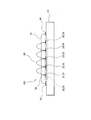
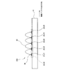
以下、図1から図3を参照して本発明の実施形態のマイクロコイル100について説明する。図1~図3に示すように、本実施形態のマイクロコイル100は、基板10の上に構成されたものであり、基板10は、複数の電極パッド21~25が所定の間隔で一列に並んだ第1電極アレイ20と、第1電極アレイ20と平行に配置され、複数の電極パッド31~35が所定の間隔で一列に並んだ第2電極アレイ30と、第1、第2電極アレイ20,30の間で、第1、第2電極アレイ20,30の電極パッド21~25、31~35の並び方向外側に配置された2つの電極台41、42を含んでいる。ここで、電極パッド21~25、31~35は、対向して配置され、電極パッド21、31を第1行、電極パッド22、32を第2行、電極パッド23、33を第3行、電極パッド24、34を第4行、電極パッド25、35を第5行の電極パッドとして説明する。
基板10は、シリコン等の材料で構成され、電極パッド21~25、31~35は周囲の基板10と絶縁された電極である。このような電極は、半導体チップの表面に形成される電極と同様の方法で形成することができる。電極パッド21~25、31~35の大きさとピッチに制限は無いが、一例をあげると、電極パッド21~25、31~35の大きさは、30~60μmの正方形で、電極パッド21~25、31~35の並び方向のピッチは、50~100μmであってもよい。
電極台41、42は、後で説明する第1ワイヤ50のループ高さよりも高さが高く、その上に磁性体70を支持できるものであれば良い。例えば、電極パッド21~25、31~35と同様の電極パッドを形成し、その上にワイヤボンディング装置でバンプを形成したものであっても良いし、電極パッドの上に所定の厚みの金属板を接合したものであってもよい。第1ワイヤ50のループ高さが、例えば、50μm程度の場合、電極台41,42の高いは、例えば、100μm程度であってもよい。
基板10の電極台41,42の上には、棒状の磁性体70が取り付けられている。磁性体70は、例えば、中心の磁性線の周囲を金属で覆った直径50μm程度の磁性ワイヤ71であっても良いし、厚さ50μm程度の平板状のフェライトであってもよい。磁性体70を磁性ワイヤ71で構成する場合、図4に示すように、電極台41、42に代えて電極パッド21~25、31~35と同様の第2の電極パッド43,44を電極台41、42の位置に配置し、ワイヤボンディングによって2つの第2の電極パッド43、44の間を磁性ワイヤ71で接続してもよい。この場合、磁性ワイヤ71は、図4に示すように、電極台41、42と同様の高さで直線状に延び、両端が2つの第2の電極パッド43,44に向かって下向きに曲がっている形状となっている。
基板10の第1電極アレイ20と第2電極アレイ30との間は、図2、図3に示すように、第1ワイヤ50と第2ワイヤ60とで接続されている。第1ワイヤ50は、第1電極アレイ20の一の行の電極パッド21~25と対向する第2電極アレイ30の一の行の電極パッド31~35との間を磁性体70の下側で接続するワイヤである。より詳しくは、第1ワイヤ50は、第1電極アレイ20の第1行の電極パッド21と第2電極アレイ30の第1行の電極パッド31とを接続するものから、第1電極アレイ20の第5行の電極パッド25と第2電極アレイ30の第5行の電極パッド35とを接続するものまでの5本のワイヤで構成されている。また、第1ワイヤ50は、金あるいは銅等の20μm~40μm程度のワイヤを、図2に示すように略台形のループ形状としたものであり、そのループ高さは、例えば、50μm程度である。
第2ワイヤ60は、磁性体70の上を跨ぐように、第2電極アレイ30の一の行の電極パッド31~34と、第1電極アレイ20の次の行の電極パッド22~25との間を前記第1ワイヤ50よりも高いループによって接続するものである。より詳しくは、第2ワイヤ60は、第2電極アレイ30の第1行の電極パッド31と第1電極アレイ20の第2行(次の行)の電極パッド22とを接続するものから、第2電極アレイ30の第4行の電極パッド34と第1電極アレイ20の第5行(次の行)の電極パッド25とを接続するものまでの4本のワイヤで構成されている。第2ワイヤ60は、第1ワイヤ50と同様、金あるいは銅等の20μm~50μm程度のワイヤである。第2ワイヤ60は、図2、図3に示すように、山形のループ形状であり、その高さは、例えば、200μm程度であってもよい。
以上のように構成された第1ワイヤ50、第2ワイヤ60は、図1から図3に示すように、磁性体70の周囲に巻回されたマイクロコイル100を構成する。
次に、図1から図3に示すマイクロコイル100を基板10の上に形成する方法について説明する。以下の説明では、説明のために各部の寸法を例示するが、異なる寸法として異なる大きさのマイクロコイル100を同様の方法で形成することが可能である。
基板10には、先に説明したように、第1電極アレイ20と、第2電極アレイ30と2つの電極台41,42が配置されている。電極台41,42を電極パッドの上にバンプを形成したものとする場合、電極台41,42の位置に配置された電極パッドの上にワイヤボンディングによって高さが100μm程度になる様に一段あるいは複数段のバンプを形成する。
基板10の第1電極アレイ20、第2電極アレイ30、電極台41,42の準備ができたら、直径30μm程度の金または銅ワイヤを用いてワイヤボンディングによって第1電極アレイ20の電極パッド21~25と第2電極アレイ30の電極パッド31~35との間を5本の第1ワイヤ50で接続する。先に説明したように、第1ワイヤ50は略台形のループ形状で50μm程度の高さとする。
次に、電極台41,42の上に磁性体70を取り付ける。電極台41,42の高さは100μm程度であるから、磁性体70は、第1ワイヤ50の上に第1ワイヤ50と離間して配置される。また、磁性体70の延びる方向と第1ワイヤ50のループの方向は直交方向となる。なお、磁性体70を磁性ワイヤ71で構成する場合には、図4に示すように、第2の電極パッド43,44の間をループ高さ100μm程度の磁性ワイヤ71で接続する。
次に、直径30μm程度の金または銅ワイヤを用いてワイヤボンディングによって、磁性体70の上を跨ぐように、第2電極アレイ30の電極パッド31~34と第1電極アレイ20の電極パッド22~24との間を4本の第2ワイヤ60で接続する。先に説明したように、第2ワイヤは、山形のループ形状で200μm程度の高さである。磁性体70の配置されている高さは、100μm程度であり、磁性体70の直径は50μm程度であるから、磁性体70と第2ワイヤ60との間には空間ができる。第2ワイヤ60の接続が終了すると基板10の上に磁性体70の周囲にワイヤが巻回されたマイクロコイル100が形成される。
以上説明したように、基板10に配置された電極パッド21~25、31~35の間をワイヤボンディングによってワイヤで接続するという簡便な方法でマイクロコイル100を構成することができる。
次に、図5を参照しながら、図1から図3を参照して説明したマイクロコイル100を応用したマイクロトランス150について説明する。図5に示すように、マイクロトランス150は、第1電極アレイ20の第1行の電極パッド21に交流電源81からの入力線80を接続し、第2電極アレイ30の第2行の電極パッド32にグランド線82を接続し、第2電極アレイ30の第5行の電極パッド35に出力線83を接続する。これにより、マイクロコイル100は、電極パッド21から電極パッド32までの1.5ターンの第1巻線と、電極パッド31から電極パッド35までの3.5ターンの第2巻線に分けられる。そして、入力線80に交流電源81を接続し、出力線83に出力端子84を接続すると、出力端子84からは、第1巻線のターン数と第2巻線のターン数に比例した電圧が出力される。
次に図6から図8を参照しながら本発明の他の実施形態のマイクロコイル200について説明する。先に図1から図3を参照して説明した実施形態と同様の部分には同様の符号を付して説明は省略する。
本実施形態のマイクロコイル200は、図1から図3を参照して説明したマイクロコイル100の磁性体70、電極台41、42がないものである。第1ワイヤ50、第2ワイヤ60の構成は、図1から図3を参照して説明したマイクロコイル100と同様である。本実施形態のマイクロコイル200は、より簡便な方法で基板10の上にマイクロコイル200を形成することができる。
次に図9を参照しながら、本発明の他の実施形態のマイクロコイル300について説明する。本実施形態では、第2電極アレイ30は、第1電極アレイ20と平行で、第1電極アレイ20の電極パッド21~25と電極パッド31~35の並び方向の位置がずれるよう配置されているものである。電極パッド21は第1電極アレイの第1行の電極パッドであり、電極パッド22~25は第1電極アレイ20の第2行~第5行の電極パッドである。また、電極パッド31は第2電極アレイ30の第1行の電極パッドであり、電極パッド32~35は第2電極アレイ30の第2行~第5行の電極パッドである。なお、本実施形態のマイクロコイル300の電極台41、42、磁性体70は、図1~図3を参照して説明した実施形態と同様である。
本実施形態でも、第1ワイヤ50は、第1電極アレイ20の一の行の電極パッド21~25と第2電極アレイ30の一の行の電極パッド31~35との間を磁性体70の下側で接続するワイヤである。より詳しくは、第1ワイヤ50は、第1電極アレイ20の第1行の電極パッド21と第2電極アレイ30の第1行の電極パッド31とを接続するものから、第1電極アレイ20の第5行の電極パッド25と第2電極アレイ30の第5行の電極パッド35とを接続するものまでの5本のワイヤで構成されている。また、第1ワイヤ50は、金あるいは銅等の20μm~40μm程度のワイヤを、図2に示すように略台形のループ形状としたものであり、そのループ高さは、例えば、50μm程度である。
また、第2ワイヤ60は、磁性体70の上を跨ぐように、第2電極アレイ30の一の行の電極パッド31~34と、第1電極アレイ20の次の行の電極パッド22~25との間を前記第1ワイヤ50よりも高いループによって接続するものである。より詳しくは、第2ワイヤ60は、第2電極アレイ30の第1行の電極パッド31と第1電極アレイ20の第2行(次の行)の電極パッド22とを接続するものから、第2電極アレイ30の第4行の電極パッド34と第1電極アレイ20の第5行(次の行)の電極パッド25とを接続するものまでの4本のワイヤで構成されている。第2ワイヤ60は、第1ワイヤ50と同様、金あるいは銅等の20μm~50μm程度のワイヤである。第2ワイヤ60は、図2、図3に示すように、山形のループ形状であり、その高さは、例えば、例えば、200μm程度であってもよい。
以上のように構成された第1ワイヤ50、第2ワイヤ60は、図9に示すように、磁性体70の周囲に巻回されたマイクロコイル300を構成する。
10 基板、20 第1電極アレイ、21~25,31~35,43,44 電極パッド、30 第2電極アレイ、41,42 電極台、50 第1ワイヤ、60 第2ワイヤ、70 磁性体、71 磁性ワイヤ、80 入力線、81 交流電源、82 グランド線、83 出力線、84 出力端子、100,200,300 マイクロコイル、150 マイクロトランス。
Claims (9)
- 複数の電極パッドが所定の間隔で一列に並んだ第1電極アレイと、前記第1電極アレイと平行で、複数の電極パッドが所定の間隔で一列に並んだ第2電極アレイと、が配置された基板と、
前記第1電極アレイの一の行の電極パッドと前記第2電極アレイの一の行の電極パッドとの間を接続する第1ワイヤと、
前記第2電極アレイの一の行の電極パッドと前記第1電極アレイの次の行の電極パッドとの間を前記第1ワイヤよりも高いループによって接続する第2ワイヤと、を有するマイクロコイル。 - 請求項1に記載のマイクロコイルであって、
前記第1電極アレイと前記第2電極アレイとの間に前記第1、第2電極アレイと平行で前記基板の表面から所定の間隔をあけて配置された磁性体を更に備え、
前記第1ワイヤは、前記磁性体の下側を通って電極パッドの間を接続し、前記第2ワイヤは、前記磁性体の上側を跨ぐように電極パッドの間を接続するマイクロコイル。 - 請求項2に記載のマイクロコイルであって、
前記基板は、前記第1、第2の電極アレイの間で、前記第1、第2の電極アレイの電極パッドの並び方向外側に配置された2つの電極台を含み、
前記磁性体は、2つの前記電極台の上に接続されていること、
を特徴とするマイクロコイル。 - 請求項2に記載のマイクロコイルであって、
前記基板は、前記第1、第2の電極アレイの間で、前記第1、第2の電極アレイの電極パッドの並び方向外側に配置された2つの第2の電極パッドを含み、
前記磁性体は、2つの前記第2の電極パッド間を接続する磁性体ワイヤであるマイクロコイル。 - 請求項1から4のいずれか1項に記載のマイクロコイルであって、
前記第2電極アレイは、前記第1電極アレイと平行で、前記第1電極アレイの電極パッドと電極パッドの並び方向の位置がずれるように複数の電極パッドが所定の間隔で一列に並んでいるマイクロコイル。 - マイクロコイルを形成する方法であって、
複数の電極パッドが所定の間隔で一列に並んだ第1電極アレイと、前記第1電極アレイと平行で、複数の電極パッドが所定の間隔で一列に並んだ第2電極アレイと、が配置された基板を準備し、
前記第1電極アレイの一の行の電極パッドと前記第2電極アレイの一の行の電極パッドとの間をワイヤボンディングにより第1ワイヤで接続し、
前記第2電極アレイの一の行の電極パッドと前記第1電極アレイの次の行の電極パッドとの間をワイヤボンディングにより前記第1ワイヤよりも高いループを有する第2ワイヤで接続する方法。 - 請求項6に記載のマイクロコイルを形成する方法であって、
前記基板は、前記第1、第2の電極アレイの間で、前記第1、第2の電極アレイの並び方向外側に2つの電極台が配置され、
前記第1電極アレイの一の行の電極パッドと前記第2電極アレイの一の行の電極パッドとの間をワイヤボンディングにより第1ワイヤで接続し、
前記第1ワイヤの上側で前記第1ワイヤと離間するように2つの前記電極台の上に磁性体を取り付け、
前記磁性体の上を跨ぐように、前記第2電極アレイの一の行の電極パッドと前記第1電極アレイの次の行の電極パッドとの間をワイヤボンディングにより第2ワイヤで接続する方法。 - 請求項6に記載のマイクロコイルを形成する方法であって、
前記基板は、前記第2電極アレイが前記第1電極アレイと平行で、前記第1電極アレイの電極パッドと電極パッドの並び方向の位置がずれるように複数の電極パッドが所定の間隔で一列に並んで配置されている方法。 - 請求項7に記載のマイクロコイルを形成する方法であって、
前記基板は、前記第2電極アレイが前記第1電極アレイと平行で、前記第1電極アレイの電極パッドと電極パッドの並び方向の位置がずれるように複数の電極パッドが所定の間隔で一列に並んで配置されている方法。
Applications Claiming Priority (2)
| Application Number | Priority Date | Filing Date | Title |
|---|---|---|---|
| JP2016-149403 | 2016-07-29 | ||
| JP2016149403A JP2018019002A (ja) | 2016-07-29 | 2016-07-29 | マイクロコイル及びその形成方法 |
Publications (1)
| Publication Number | Publication Date |
|---|---|
| WO2018021470A1 true WO2018021470A1 (ja) | 2018-02-01 |
Family
ID=61016886
Family Applications (1)
| Application Number | Title | Priority Date | Filing Date |
|---|---|---|---|
| PCT/JP2017/027231 Ceased WO2018021470A1 (ja) | 2016-07-29 | 2017-07-27 | マイクロコイル及びその形成方法 |
Country Status (3)
| Country | Link |
|---|---|
| JP (1) | JP2018019002A (ja) |
| TW (1) | TW201804485A (ja) |
| WO (1) | WO2018021470A1 (ja) |
Citations (2)
| Publication number | Priority date | Publication date | Assignee | Title |
|---|---|---|---|---|
| US20050122198A1 (en) * | 2003-12-05 | 2005-06-09 | Yaping Zhou | Inductive device including bond wires |
| JP2016018817A (ja) * | 2014-07-04 | 2016-02-01 | ローム株式会社 | 半導体装置 |
-
2016
- 2016-07-29 JP JP2016149403A patent/JP2018019002A/ja active Pending
-
2017
- 2017-07-27 TW TW106125311A patent/TW201804485A/zh unknown
- 2017-07-27 WO PCT/JP2017/027231 patent/WO2018021470A1/ja not_active Ceased
Patent Citations (2)
| Publication number | Priority date | Publication date | Assignee | Title |
|---|---|---|---|---|
| US20050122198A1 (en) * | 2003-12-05 | 2005-06-09 | Yaping Zhou | Inductive device including bond wires |
| JP2016018817A (ja) * | 2014-07-04 | 2016-02-01 | ローム株式会社 | 半導体装置 |
Also Published As
| Publication number | Publication date |
|---|---|
| JP2018019002A (ja) | 2018-02-01 |
| TW201804485A (zh) | 2018-02-01 |
Similar Documents
| Publication | Publication Date | Title |
|---|---|---|
| US7868729B2 (en) | Stacked device assembly with integrated coil and method of forming same | |
| CN105814687B (zh) | 半导体封装及其安装结构 | |
| US9818709B2 (en) | Semiconductor device and manufacturing method thereof | |
| JP2014530511A5 (ja) | ||
| US10679972B2 (en) | Method of manufacturing multi-chip package | |
| CN103000608B (zh) | 一种多组件的芯片封装结构 | |
| JP3566957B2 (ja) | 半導体装置及びその製造方法 | |
| TW201312723A (zh) | 晶片封裝結構及其製造方法 | |
| JP6292300B2 (ja) | コイル部品およびこのコイル部品を備えるモジュール | |
| US8710667B2 (en) | Semiconductor device | |
| US20170273185A1 (en) | Fabrication method of circuit structure | |
| US20130093072A1 (en) | Leadframe pad design with enhanced robustness to die crack failure | |
| US20130256889A1 (en) | Substrate and semiconductor device | |
| CN107708300A (zh) | 电子堆迭结构及其制法 | |
| KR100648040B1 (ko) | 다수의 금속 랜드를 가지는 인터포저 기판, 및 이로부터제작되는 인터포저를 포함하는 적층 칩 패키지 | |
| US8399998B2 (en) | Semiconductor package requiring reduced manufacturing processes | |
| JP2018019002A (ja) | マイクロコイル及びその形成方法 | |
| US20140167251A1 (en) | Semiconductor device, semiconductor module, and manufacturing method for semiconductor device | |
| JP2004363224A (ja) | 半導体チップの接続構造 | |
| JP2014120501A (ja) | 半導体装置及び半導体装置の製造方法 | |
| US6965162B2 (en) | Semiconductor chip mounting substrate and semiconductor device using it | |
| KR101239458B1 (ko) | 계단식 적층구조를 갖는 반도체 패키지 및 그의 제조방법 | |
| JP2005259969A (ja) | 半導体装置およびその製造方法 | |
| TWI591667B (zh) | 軟式電路板 | |
| KR101069460B1 (ko) | 반도체 디바이스 및 그 제조 방법 |
Legal Events
| Date | Code | Title | Description |
|---|---|---|---|
| 121 | Ep: the epo has been informed by wipo that ep was designated in this application |
Ref document number: 17834472 Country of ref document: EP Kind code of ref document: A1 |
|
| NENP | Non-entry into the national phase |
Ref country code: DE |
|
| 122 | Ep: pct application non-entry in european phase |
Ref document number: 17834472 Country of ref document: EP Kind code of ref document: A1 |