WO2018020871A1 - 光電変換素子、撮像素子、光センサ、化合物 - Google Patents
光電変換素子、撮像素子、光センサ、化合物 Download PDFInfo
- Publication number
- WO2018020871A1 WO2018020871A1 PCT/JP2017/021732 JP2017021732W WO2018020871A1 WO 2018020871 A1 WO2018020871 A1 WO 2018020871A1 JP 2017021732 W JP2017021732 W JP 2017021732W WO 2018020871 A1 WO2018020871 A1 WO 2018020871A1
- Authority
- WO
- WIPO (PCT)
- Prior art keywords
- atom
- formula
- group
- substituent
- photoelectric conversion
- Prior art date
- Legal status (The legal status is an assumption and is not a legal conclusion. Google has not performed a legal analysis and makes no representation as to the accuracy of the status listed.)
- Ceased
Links
Images





Classifications
-
- C—CHEMISTRY; METALLURGY
- C07—ORGANIC CHEMISTRY
- C07D—HETEROCYCLIC COMPOUNDS
- C07D471/00—Heterocyclic compounds containing nitrogen atoms as the only ring hetero atoms in the condensed system, at least one ring being a six-membered ring with one nitrogen atom, not provided for by groups C07D451/00 - C07D463/00
- C07D471/02—Heterocyclic compounds containing nitrogen atoms as the only ring hetero atoms in the condensed system, at least one ring being a six-membered ring with one nitrogen atom, not provided for by groups C07D451/00 - C07D463/00 in which the condensed system contains two hetero rings
- C07D471/04—Ortho-condensed systems
-
- C—CHEMISTRY; METALLURGY
- C07—ORGANIC CHEMISTRY
- C07D—HETEROCYCLIC COMPOUNDS
- C07D519/00—Heterocyclic compounds containing more than one system of two or more relevant hetero rings condensed among themselves or condensed with a common carbocyclic ring system not provided for in groups C07D453/00 or C07D455/00
-
- H—ELECTRICITY
- H10—SEMICONDUCTOR DEVICES; ELECTRIC SOLID-STATE DEVICES NOT OTHERWISE PROVIDED FOR
- H10F—INORGANIC SEMICONDUCTOR DEVICES SENSITIVE TO INFRARED RADIATION, LIGHT, ELECTROMAGNETIC RADIATION OF SHORTER WAVELENGTH OR CORPUSCULAR RADIATION
- H10F30/00—Individual radiation-sensitive semiconductor devices in which radiation controls the flow of current through the devices, e.g. photodetectors
- H10F30/20—Individual radiation-sensitive semiconductor devices in which radiation controls the flow of current through the devices, e.g. photodetectors the devices having potential barriers, e.g. phototransistors
-
- H—ELECTRICITY
- H10—SEMICONDUCTOR DEVICES; ELECTRIC SOLID-STATE DEVICES NOT OTHERWISE PROVIDED FOR
- H10F—INORGANIC SEMICONDUCTOR DEVICES SENSITIVE TO INFRARED RADIATION, LIGHT, ELECTROMAGNETIC RADIATION OF SHORTER WAVELENGTH OR CORPUSCULAR RADIATION
- H10F39/00—Integrated devices, or assemblies of multiple devices, comprising at least one element covered by group H10F30/00, e.g. radiation detectors comprising photodiode arrays
- H10F39/10—Integrated devices
- H10F39/12—Image sensors
- H10F39/191—Photoconductor image sensors
-
- H—ELECTRICITY
- H10—SEMICONDUCTOR DEVICES; ELECTRIC SOLID-STATE DEVICES NOT OTHERWISE PROVIDED FOR
- H10K—ORGANIC ELECTRIC SOLID-STATE DEVICES
- H10K30/00—Organic devices sensitive to infrared radiation, light, electromagnetic radiation of shorter wavelength or corpuscular radiation
-
- H—ELECTRICITY
- H10—SEMICONDUCTOR DEVICES; ELECTRIC SOLID-STATE DEVICES NOT OTHERWISE PROVIDED FOR
- H10K—ORGANIC ELECTRIC SOLID-STATE DEVICES
- H10K39/00—Integrated devices, or assemblies of multiple devices, comprising at least one organic radiation-sensitive element covered by group H10K30/00
- H10K39/30—Devices controlled by radiation
- H10K39/32—Organic image sensors
-
- H—ELECTRICITY
- H10—SEMICONDUCTOR DEVICES; ELECTRIC SOLID-STATE DEVICES NOT OTHERWISE PROVIDED FOR
- H10K—ORGANIC ELECTRIC SOLID-STATE DEVICES
- H10K85/00—Organic materials used in the body or electrodes of devices covered by this subclass
- H10K85/60—Organic compounds having low molecular weight
- H10K85/615—Polycyclic condensed aromatic hydrocarbons, e.g. anthracene
- H10K85/626—Polycyclic condensed aromatic hydrocarbons, e.g. anthracene containing more than one polycyclic condensed aromatic rings, e.g. bis-anthracene
-
- H—ELECTRICITY
- H10—SEMICONDUCTOR DEVICES; ELECTRIC SOLID-STATE DEVICES NOT OTHERWISE PROVIDED FOR
- H10K—ORGANIC ELECTRIC SOLID-STATE DEVICES
- H10K85/00—Organic materials used in the body or electrodes of devices covered by this subclass
- H10K85/60—Organic compounds having low molecular weight
- H10K85/649—Aromatic compounds comprising a hetero atom
- H10K85/653—Aromatic compounds comprising a hetero atom comprising only oxygen as heteroatom
-
- H—ELECTRICITY
- H10—SEMICONDUCTOR DEVICES; ELECTRIC SOLID-STATE DEVICES NOT OTHERWISE PROVIDED FOR
- H10K—ORGANIC ELECTRIC SOLID-STATE DEVICES
- H10K85/00—Organic materials used in the body or electrodes of devices covered by this subclass
- H10K85/60—Organic compounds having low molecular weight
- H10K85/649—Aromatic compounds comprising a hetero atom
- H10K85/655—Aromatic compounds comprising a hetero atom comprising only sulfur as heteroatom
-
- H—ELECTRICITY
- H10—SEMICONDUCTOR DEVICES; ELECTRIC SOLID-STATE DEVICES NOT OTHERWISE PROVIDED FOR
- H10K—ORGANIC ELECTRIC SOLID-STATE DEVICES
- H10K85/00—Organic materials used in the body or electrodes of devices covered by this subclass
- H10K85/60—Organic compounds having low molecular weight
- H10K85/649—Aromatic compounds comprising a hetero atom
- H10K85/656—Aromatic compounds comprising a hetero atom comprising two or more different heteroatoms per ring
-
- H—ELECTRICITY
- H10—SEMICONDUCTOR DEVICES; ELECTRIC SOLID-STATE DEVICES NOT OTHERWISE PROVIDED FOR
- H10K—ORGANIC ELECTRIC SOLID-STATE DEVICES
- H10K85/00—Organic materials used in the body or electrodes of devices covered by this subclass
- H10K85/60—Organic compounds having low molecular weight
- H10K85/649—Aromatic compounds comprising a hetero atom
- H10K85/657—Polycyclic condensed heteroaromatic hydrocarbons
-
- H—ELECTRICITY
- H10—SEMICONDUCTOR DEVICES; ELECTRIC SOLID-STATE DEVICES NOT OTHERWISE PROVIDED FOR
- H10K—ORGANIC ELECTRIC SOLID-STATE DEVICES
- H10K85/00—Organic materials used in the body or electrodes of devices covered by this subclass
- H10K85/60—Organic compounds having low molecular weight
- H10K85/649—Aromatic compounds comprising a hetero atom
- H10K85/657—Polycyclic condensed heteroaromatic hydrocarbons
- H10K85/6572—Polycyclic condensed heteroaromatic hydrocarbons comprising only nitrogen in the heteroaromatic polycondensed ring system, e.g. phenanthroline or carbazole
-
- H—ELECTRICITY
- H10—SEMICONDUCTOR DEVICES; ELECTRIC SOLID-STATE DEVICES NOT OTHERWISE PROVIDED FOR
- H10K—ORGANIC ELECTRIC SOLID-STATE DEVICES
- H10K85/00—Organic materials used in the body or electrodes of devices covered by this subclass
- H10K85/60—Organic compounds having low molecular weight
- H10K85/649—Aromatic compounds comprising a hetero atom
- H10K85/657—Polycyclic condensed heteroaromatic hydrocarbons
- H10K85/6576—Polycyclic condensed heteroaromatic hydrocarbons comprising only sulfur in the heteroaromatic polycondensed ring system, e.g. benzothiophene
-
- H—ELECTRICITY
- H10—SEMICONDUCTOR DEVICES; ELECTRIC SOLID-STATE DEVICES NOT OTHERWISE PROVIDED FOR
- H10K—ORGANIC ELECTRIC SOLID-STATE DEVICES
- H10K30/00—Organic devices sensitive to infrared radiation, light, electromagnetic radiation of shorter wavelength or corpuscular radiation
- H10K30/30—Organic devices sensitive to infrared radiation, light, electromagnetic radiation of shorter wavelength or corpuscular radiation comprising bulk heterojunctions, e.g. interpenetrating networks of donor and acceptor material domains
-
- H—ELECTRICITY
- H10—SEMICONDUCTOR DEVICES; ELECTRIC SOLID-STATE DEVICES NOT OTHERWISE PROVIDED FOR
- H10K—ORGANIC ELECTRIC SOLID-STATE DEVICES
- H10K85/00—Organic materials used in the body or electrodes of devices covered by this subclass
- H10K85/30—Coordination compounds
- H10K85/321—Metal complexes comprising a group IIIA element, e.g. Tris (8-hydroxyquinoline) gallium [Gaq3]
- H10K85/322—Metal complexes comprising a group IIIA element, e.g. Tris (8-hydroxyquinoline) gallium [Gaq3] comprising boron
-
- H—ELECTRICITY
- H10—SEMICONDUCTOR DEVICES; ELECTRIC SOLID-STATE DEVICES NOT OTHERWISE PROVIDED FOR
- H10K—ORGANIC ELECTRIC SOLID-STATE DEVICES
- H10K85/00—Organic materials used in the body or electrodes of devices covered by this subclass
- H10K85/60—Organic compounds having low molecular weight
- H10K85/649—Aromatic compounds comprising a hetero atom
-
- H—ELECTRICITY
- H10—SEMICONDUCTOR DEVICES; ELECTRIC SOLID-STATE DEVICES NOT OTHERWISE PROVIDED FOR
- H10K—ORGANIC ELECTRIC SOLID-STATE DEVICES
- H10K85/00—Organic materials used in the body or electrodes of devices covered by this subclass
- H10K85/60—Organic compounds having low molecular weight
- H10K85/649—Aromatic compounds comprising a hetero atom
- H10K85/657—Polycyclic condensed heteroaromatic hydrocarbons
- H10K85/6574—Polycyclic condensed heteroaromatic hydrocarbons comprising only oxygen in the heteroaromatic polycondensed ring system, e.g. cumarine dyes
-
- Y—GENERAL TAGGING OF NEW TECHNOLOGICAL DEVELOPMENTS; GENERAL TAGGING OF CROSS-SECTIONAL TECHNOLOGIES SPANNING OVER SEVERAL SECTIONS OF THE IPC; TECHNICAL SUBJECTS COVERED BY FORMER USPC CROSS-REFERENCE ART COLLECTIONS [XRACs] AND DIGESTS
- Y02—TECHNOLOGIES OR APPLICATIONS FOR MITIGATION OR ADAPTATION AGAINST CLIMATE CHANGE
- Y02E—REDUCTION OF GREENHOUSE GAS [GHG] EMISSIONS, RELATED TO ENERGY GENERATION, TRANSMISSION OR DISTRIBUTION
- Y02E10/00—Energy generation through renewable energy sources
- Y02E10/50—Photovoltaic [PV] energy
- Y02E10/549—Organic PV cells
Definitions
- the present invention relates to a photoelectric conversion element, an imaging element, an optical sensor, and a compound.
- a planar solid-state imaging device in which photodiodes (PD) are two-dimensionally arranged and signal charges generated in each PD are read by a circuit has been widely used.
- a structure in which a color filter that transmits light of a specific wavelength is arranged on the light incident surface side of the flat solid-state imaging device is generally used.
- a single-plate type solid-state imaging device in which color filters that transmit blue (B) light, green (G) light, and red (R) light are regularly arranged on each PD arranged two-dimensionally is often used.
- B blue
- G green
- R red
- Patent Document 1 discloses a photoelectric conversion element having a photoelectric conversion film containing the following compound.
- This inventor produced a photoelectric conversion element using the compound (for example, the compound mentioned above) specifically disclosed by patent document 1, and the responsiveness of the obtained photoelectric conversion element, and heat resistance (heating) As a result of examination of the response after processing, it was found that the characteristics did not necessarily reach the level required recently, and further improvement is necessary.
- An object of this invention is to provide the photoelectric conversion element which shows the outstanding responsiveness and the outstanding heat resistance in view of the said situation.
- Another object of the present invention is to provide an image sensor and a photosensor including a photoelectric conversion element. Furthermore, this invention also aims at providing the compound applied to the said photoelectric conversion element.
- the present inventor has found that the above problems can be solved by using a photoelectric conversion film containing a compound (quinacridone) having a predetermined structure, and has completed the present invention. That is, the above problems can be solved by the following means.
- B 1 and B 2 independently represent any of an alkyl group, an aryl group, and a heteroaryl group in formula (1).
- both A 1 and A 2 represent any of the substituents represented by formulas (1f) to (1h) described later, according to (1) or (2) Photoelectric conversion element.
- both A 1 and A 2 represent any of the substituents represented by formulas (1a) to (1e) and formula (1i) described later, (1) The photoelectric conversion element according to any one of (3) to (3).
- both A 1 and A 2 are a substituent represented by the formula (1a), a substituent represented by the formula (1b), and a substituent represented by the formula (1e).
- the photoelectric conversion element according to (4) which represents any of the substituents represented by the formula (1i).
- both A 1 and A 2 are represented by the substituent represented by formula (1a), the substituent represented by formula (1b), and formula (1i).
- the photoelectric conversion element according to (4) or (5) which represents any one of the substituents.
- R 1 to R 8 each independently represents a hydrogen atom or a substituent.
- B 1 and B 2 each independently represents a hydrogen atom or a substituent.
- a 1 and A 2 each independently represent a hydrogen atom or a substituent, at least one of A 1 and A 2 has the formula (1a) ⁇ (1e), and the substituent represented by formula (1i) Represents one of the following. Further, adjacent groups among R 1 to R 8 , A 1 , A 2 , B 1 and B 2 may be linked to form a ring.
- R a1 to R a5 each independently represent a hydrogen atom, an alkyl group, an aryl group, a heteroaryl group, an alkoxy group, an alkylthio group, an ethynyl group, an ethenyl group, an acyl group, a halogen atom, or Represents a silyl group, and at least one of R a1 to R a5 represents any one of a fluorine atom, a chlorine atom, a bromine atom, a fluoroalkyl group, and a silyl group.
- R b1 to R b7 each independently represents a hydrogen atom or a substituent. * Represents a bonding position. Further, adjacent groups among R b1 to R b7 may be linked to form a ring.
- R c1 and R c2 each independently represent a hydrogen atom or a substituent. R c1 and R c2 may be connected to each other to form a ring.
- Y C1 represents a sulfur atom, an oxygen atom, a selenium atom, NR c3 , or CR c4 R c5 .
- R c3 to R c5 each independently represents a hydrogen atom or a substituent. * Represents a bonding position.
- R d1 to R d3 each independently represents a hydrogen atom or a substituent.
- Y d1 represents a sulfur atom, an oxygen atom, a selenium atom, NR d4 , or CR d5 R d6 .
- Z d1 represents a sulfur atom, an oxygen atom, a selenium atom, NR d7 , CR d8 R d9 , or R d10 C ⁇ CR d11 .
- R d4 to R d11 each independently represents a hydrogen atom or a substituent. * Represents a bonding position.
- R d1 and R d2 , R d2 and R d10, or R d2 and R d11 may be linked to each other to form a ring.
- X e1 represents a nitrogen atom or CR e2 .
- Y e1 represents a sulfur atom, an oxygen atom, a selenium atom, NR e3 , or CR e4 R e5 .
- R e1 to R e6 each independently represents a hydrogen atom or a substituent.
- R e1 and R e2 may be connected to each other to form a ring. * Represents a bonding position.
- R i1 and R i2 each independently represent a hydrogen atom, an alkyl group, an aryl group, or a heteroaryl group.
- Y i1 represents an oxygen atom, a selenium atom, NR i3 , or CR i4 R i5 .
- R i3 to R i5 each independently represents a hydrogen atom or a substituent. * Represents a bonding position.
- the photoelectric conversion element which shows the outstanding responsiveness and the outstanding heat resistance can be provided.
- the image pick-up element and optical sensor containing a photoelectric conversion element can also be provided.
- the compound applied to the said photoelectric conversion element can also be provided.
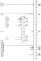
- 2 is a 1 H NMR (Nuclear Magnetic Resonance) chart of the compound (D-1).
- 2 is a 1 H NMR (Nuclear Magnetic Resonance) chart of the compound (D-7).
- 2 is a 1 H NMR (Nuclear Magnetic Resonance) chart of the compound (D-8).
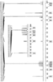
- 1 is a 1 H NMR (Nuclear Magnetic Resonance) chart of the compound (D-10).
- 1 is a 1 H NMR (Nuclear Magnetic Resonance) chart of the compound (D-11).
- 2 is a 1 H NMR (Nuclear Magnetic Resonance) chart of the compound (D-12).
- 2 is a 1 H NMR (Nuclear Magnetic Resonance) chart of the compound (D-13).
- the group is further substituted with a substituent (preferably, substituent W described later) as long as the intended effect is not impaired. It may be.
- a substituent preferably, substituent W described later
- the expression “alkyl group” corresponds to an alkyl group that may be substituted by a substituent (preferably, substituent W).
- a numerical range expressed using “to” means a range including numerical values described before and after “to” as a lower limit value and an upper limit value.
- the characteristic point compared with the prior art of the present invention is that a compound having a predetermined structure (hereinafter, also simply referred to as “specific quinacridone compound”) is used.
- a specific quinacridone compound a specific functional group is introduced at a specific position.
- the characteristics (responsiveness and heat resistance) of a photoelectric conversion element having a photoelectric conversion film containing the specific quinacridone compound are improved. ing.
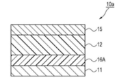
- FIG. 1A the cross-sectional schematic diagram of one Embodiment of the photoelectric conversion element of this invention is shown.
- a photoelectric conversion element 10a shown in FIG. 1A includes a conductive film (hereinafter also referred to as a lower electrode) 11 that functions as a lower electrode, an electron blocking film 16A, and a photoelectric conversion that includes a compound represented by formula (1) described later.
- the film 12 and a transparent conductive film (hereinafter also referred to as an upper electrode) 15 functioning as an upper electrode are stacked in this order.
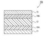
- FIG. 1B shows a configuration example of another photoelectric conversion element.
- FIGS. 1A and 1B has a configuration in which an electron blocking film 16A, a photoelectric conversion film 12, a hole blocking film 16B, and an upper electrode 15 are stacked on the lower electrode 11 in this order. Note that the stacking order of the electron blocking film 16A, the photoelectric conversion film 12, and the hole blocking film 16B in FIGS. 1A and 1B may be changed as appropriate according to the application and characteristics.
- the photoelectric conversion element 10 a it is preferable that light is incident on the photoelectric conversion film 12 via the upper electrode 15. Moreover, when using the photoelectric conversion element 10a (or 10b), a voltage can be applied. In this case, it is preferable that the lower electrode 11 and the upper electrode 15 form a pair of electrodes, and a voltage of 1 ⁇ 10 ⁇ 5 to 1 ⁇ 10 7 V / cm is applied between the pair of electrodes. From the viewpoint of performance and power consumption, a voltage of 1 ⁇ 10 ⁇ 4 to 1 ⁇ 10 7 V / cm is more preferable, and a voltage of 1 ⁇ 10 ⁇ 3 to 5 ⁇ 10 6 V / cm is more preferable.
- the photoelectric conversion element 10a (or 10b) is used as an optical sensor, or when it is incorporated into an image sensor, a voltage can be applied by the same method.
- the photoelectric conversion element 10a (or 10b) can be suitably applied to an imaging element application and an optical sensor application.
- FIG. 2 the cross-sectional schematic diagram of another embodiment of the photoelectric conversion element of this invention is shown.
- the photoelectric conversion element 200 shown in FIG. 2 is a hybrid photoelectric conversion element including an organic photoelectric conversion film 209 and an inorganic photoelectric conversion film 201.
- the organic photoelectric conversion film 209 includes a compound represented by the formula (1) described later.
- the inorganic photoelectric conversion film 201 has an n-type well 202, a p-type well 203, and an n-type well 204 on a p-type silicon substrate 205.
- Blue light is photoelectrically converted at the pn junction formed between the p-type well 203 and the n-type well 204 (B pixel), and the pn junction formed between the p-type well 203 and the n-type well 202 is converted into a pn junction.
- the red light is photoelectrically converted (R pixel). Note that the conductivity types of the n-type well 202, the p-type well 203, and the n-type well 204 are not limited to these.
- a transparent insulating layer 207 is disposed on the inorganic photoelectric conversion film 201.
- a transparent pixel electrode 208 divided for each pixel is disposed.
- an organic photoelectric conversion film 209 that absorbs green light and performs photoelectric conversion is disposed in a single configuration in common with each pixel.
- an electron blocking film 212 is arranged in a single sheet common to each pixel.
- a single transparent electrode 210 is arranged.
- a transparent protective film 211 is disposed on the uppermost layer. The stacking order of the electron blocking film 212 and the organic photoelectric conversion film 209 may be opposite to that shown in FIG. 2, and the common electrode 210 may be divided for each pixel.
- the organic photoelectric conversion film 209 constitutes a G pixel that detects green light.
- the pixel electrode 208 is the same as the lower electrode 11 of the photoelectric conversion element 10a shown in FIG. 1A.
- the common electrode 210 is the same as the upper electrode 15 of the photoelectric conversion element 10a illustrated in FIG. 1A.
- Blue light having a short wavelength is photoelectrically converted mainly in the shallow part of the semiconductor substrate (inorganic photoelectric conversion film) 201 (near the pn junction formed between the p-type well 203 and the n-type well 204) to generate photocharges.
- the signal is output to the outside.
- Red light having a long wavelength is photoelectrically converted mainly in the deep part of the semiconductor substrate (inorganic photoelectric conversion film) 201 (near the pn junction formed between the p-type well 203 and the n-type well 202), and photocharge is generated.
- a signal is output to the outside.
- a signal readout circuit (a charge transfer path in the case of a CCD (Charge-Coupled Device) type, CMOS (Complementary-Metal-Oxide-Semiconductor) is provided on the surface of the p-type silicon substrate 205. If it is a type, a MOS (Metal-Oxide-Semiconductor) transistor circuit or a green signal charge storage region is formed, and the pixel electrode 208 is connected to a corresponding green signal charge storage region by a vertical wiring.
- CCD Charge-Coupled Device
- CMOS Complementary-Metal-Oxide-Semiconductor
- the photoelectric conversion film 12 (or the organic photoelectric conversion film 209) is a film containing a compound represented by the formula (1) as a photoelectric conversion material. By using this compound, a photoelectric conversion element exhibiting excellent responsiveness and heat resistance can be obtained.
- the compound represented by Formula (1) will be described in detail.
- R 1 to R 8 each independently represents a hydrogen atom or a substituent.
- the definition of the said substituent is synonymous with the substituent W mentioned later.
- R 1 to R 8 are each independently a hydrogen atom in terms of more excellent responsiveness and / or heat resistance of the photoelectric conversion element (hereinafter also referred to simply as “a more excellent effect of the present invention”).
- An alkyl group, an alkoxy group, or a halogen atom is preferable, and a hydrogen atom is more preferable.
- adjacent groups among R 1 to R 8 , A 1 , A 2 , B 1 and B 2 may be linked to form a ring.
- the kind of ring formed is not particularly limited, and may be an aromatic ring or a non-aromatic ring, and is preferably an aromatic ring.
- the ring may be a single ring or a condensed ring composed of two or more rings.
- the aromatic ring may be an aromatic hydrocarbon ring or an aromatic heterocyclic ring.
- B 1 and B 2 each independently represents a hydrogen atom or a substituent.
- the definition of the said substituent is synonymous with the substituent W mentioned later.
- B 1 and B 2 are each independently an alkyl group, an aryl group, or, is preferably a heteroaryl group, both of B 1 and B 2 are alkyl More preferably, it is a group.
- B 1 and B 2 are preferably the same group. For example, there is a case where both B 1 and B 2 represent a methyl group.
- the number of carbon atoms in the alkyl group is not particularly limited, and is preferably 1 to 12, more preferably 1 to 8, still more preferably 1 to 6, and particularly preferably 1 to 4 in that the effects of the present invention are more excellent.
- the alkyl group may be linear, branched, or cyclic. Examples of the alkyl group include a methyl group, an ethyl group, an n-propyl group, an i-propyl group, an n-butyl group, an n-hexyl group, and a cyclohexyl group.
- the number of carbon atoms in the aryl group is not particularly limited, and is preferably 6 to 30, and more preferably 6 to 18 in terms of more excellent effects of the present invention.
- the aryl group may be a monocyclic structure or a condensed ring structure in which two or more rings are condensed (fused ring structure).
- the aryl group may be substituted with a substituent (preferably, a substituent W described later).
- aryl group examples include a phenyl group, a naphthyl group, an anthryl group, a pyrenyl group, a phenanthrenyl group, a methylphenyl group, a dimethylphenyl group, a biphenyl group, and a fluorenyl group.
- a phenyl group, a naphthyl group, or An anthryl group is preferred.
- the number of carbon atoms in the heteroaryl group is not particularly limited, and is preferably 3 to 30, and more preferably 3 to 18, from the viewpoint that the effect of the present invention is more excellent.
- the heteroaryl group may be substituted with a substituent (preferably, a substituent W described later).
- a heteroaryl group includes heteroatoms in addition to carbon and hydrogen atoms. Examples of the hetero atom include a nitrogen atom, a sulfur atom, an oxygen atom, a selenium atom, a tellurium atom, a phosphorus atom, a silicon atom, and a boron atom, and a nitrogen atom, a sulfur atom, or an oxygen atom is preferable.
- the number of heteroatoms contained in the heteroaryl group is not particularly limited, and is usually about 1 to 10, preferably 1 to 4, and more preferably 1 to 2.
- the number of ring members of the heteroaryl group is not particularly limited, preferably 3 to 8 membered rings, more preferably 5 to 7 membered rings, and further preferably 5 to 6 membered rings.
- the heteroaryl group may be a monocyclic structure or a condensed ring structure in which two or more rings are condensed. In the case of a condensed ring structure, an aromatic hydrocarbon ring not containing a hetero atom (for example, a benzene ring) may be contained.
- heteroaryl groups include pyridyl, quinolyl, isoquinolyl, acridinyl, phenanthridinyl, pteridinyl, pyrazinyl, quinoxalinyl, pyrimidinyl, quinazolyl, pyridazinyl, cinnolinyl, phthalazinyl, Triazinyl group, oxazolyl group, benzoxazolyl group, thiazolyl group, benzothiazolyl group, imidazolyl group, benzoimidazolyl group, pyrazolyl group, indazolyl group, isoxazolyl group, benzisoxazolyl group, isothiazolyl group, benzoisothiazolyl group, oxadiazolyl Group, thiadiazolyl group, triazolyl group, tetrazolyl group, furyl group, benzofuryl group, thienyl group, be
- a 1 and A 2 each independently represents a hydrogen atom or a substituent, and at least one of A 1 and A 2 represents any of the substituents represented by formulas (1f) to (1h).
- the definition of the said substituent is synonymous with the substituent W mentioned later.
- both A 1 and A 2 represent any of the substituents represented by the formulas (1f) to (1h) in that the effect of the present invention is more excellent.
- both of A 1 and A 2 are preferably represent the same group. For example, there is a case where both A 1 and A 2 represent a group represented by the formula (1f) in which R f1 to R f5 are all hydrogen atoms.
- R f1 to R f5 each independently represent a hydrogen atom, an alkyl group, an aryl group, a heteroaryl group, an alkoxy group, an alkylthio group, an ethynyl group, an ethenyl group, an acyl group, a halogen atom, or Represents a silyl group. * Represents a bonding position.
- each said group may have a substituent further.
- the alkyl group may be a fluoroalkyl group. That is, the alkyl group is an alkyl group that may be substituted with a fluorine atom.
- the fluoroalkyl group is a group in which at least one hydrogen atom in the alkyl group is substituted with a fluorine atom, and is preferably a group in which all the hydrogen atoms in the alkyl group are substituted with fluorine atoms.
- the number of carbon atoms in the fluoroalkyl group is not particularly limited, and is preferably 1 to 10, more preferably 1 to 6, still more preferably 1 to 3, and particularly preferably 1 from the viewpoint that the effects of the present invention are more excellent.
- the fluoroalkyl group may be linear, branched, or cyclic.
- the silyl group is a group represented by —Si (R x ) 3 (R x represents a hydrogen atom or a substituent, and three R x may be the same or different).
- R x is preferably an alkyl group or an aryl group.
- the number of carbon atoms in the alkyl group is not particularly limited and is preferably 1 to 3.
- X g1 represents a nitrogen atom or CR g3 .
- Y g1 represents a sulfur atom, an oxygen atom, a selenium atom, NR g4 , CR g5 R g6 , or R g7 C ⁇ CR g8 .
- R g1 to R g8 each independently represents a hydrogen atom or a substituent. The definition of a substituent is synonymous with the substituent W mentioned later. * Represents a bonding position.
- adjacent groups among R g1 to R g8 may be linked to form a ring.
- the ring formed by connecting adjacent groups among R g1 to R g8 may be an aromatic ring or a non-aromatic ring.
- the ring may be a single ring or a condensed ring composed of two or more rings.
- the aromatic ring may be an aromatic hydrocarbon ring or an aromatic heterocyclic ring.
- the ring formed by linking adjacent groups among R g1 to R g8 is preferred in that the effect of the present invention is more excellent, and an aromatic ring is preferred, an aromatic hydrocarbon ring is more preferred, and benzene Rings are more preferred.
- the ring formed by linking adjacent groups among R g1 to R g8 may be substituted with a substituent.
- the definition of a substituent is synonymous with the substituent W mentioned later.
- X h1 represents a nitrogen atom or CR h3 .
- Y h1 represents a sulfur atom, an oxygen atom, a selenium atom, NR h4 , or CR h5 R h6 .
- R h1 to R h6 each independently represents a hydrogen atom or a substituent. The definition of a substituent is synonymous with the substituent W mentioned later. * Represents a bonding position.
- adjacent groups among R h1 to R h6 may be linked to form a ring.
- the ring formed by connecting adjacent groups among R h1 to R h6 may be an aromatic ring or a non-aromatic ring.
- the ring may be a single ring or a condensed ring composed of two or more rings.
- the aromatic ring may be an aromatic hydrocarbon ring or an aromatic heterocyclic ring.
- the ring formed by connecting adjacent groups among R h1 to R h6 is preferable in terms of more excellent effects of the present invention, preferably an aromatic ring, more preferably an aromatic hydrocarbon ring, and benzene. Rings are more preferred.
- the ring formed by linking adjacent groups among R g1 to R g8 may be substituted with a substituent.
- the definition of a substituent is synonymous with the substituent W mentioned later.
- the substituent represented by the said Formula (1f) As a suitable aspect of the substituent represented by the said Formula (1f), the substituent represented by Formula (1a) is mentioned. Moreover, as a suitable aspect of the substituent represented by said Formula (1g), the substituent represented by Formula (1b) and the substituent represented by Formula (1e) are mentioned. Furthermore, preferred embodiments of the substituent represented by the formula (1h) include a substituent represented by the formula (1c), a substituent represented by the formula (1d), and a formula (1i). Substituents. Among them, A 1 and A 2 are represented by the substituent represented by the formula (1a), the substituent represented by the formula (1b), and the formula (1e) in that the effect of the present invention is more excellent.
- R a1 to R a5 each independently represent a hydrogen atom, an alkyl group, an aryl group, a heteroaryl group, an alkoxy group, an alkylthio group, an ethynyl group, an ethenyl group, an acyl group, a halogen atom, or Represents a silyl group, and at least one of R a1 to R a5 represents any one of a fluorine atom, a chlorine atom, a bromine atom, a fluoroalkyl group, and a silyl group.
- R a1 to R a5 represent any one of a fluorine atom, a chlorine atom, a bromine atom, a fluoroalkyl group, and a silyl group.
- at least one of R a1 to R a5 is preferably a fluorine atom or a fluoroalkyl group from the viewpoint of more excellent effects of the present invention.
- R b1 to R b7 each independently represents a hydrogen atom or a substituent. * Represents a bonding position.
- the definition of the said substituent is synonymous with the substituent W mentioned later.
- adjacent groups among R b1 to R b7 may be linked to form a ring.
- the ring formed by connecting adjacent groups among R b1 to R b7 may be an aromatic ring or a non-aromatic ring.
- the ring may be a single ring or a condensed ring composed of two or more rings.
- the aromatic ring may be an aromatic hydrocarbon ring or an aromatic heterocyclic ring.
- the ring formed by connecting adjacent groups among R b1 to R b7 is preferable in view of more excellent effects of the present invention, preferably an aromatic ring, more preferably an aromatic hydrocarbon ring, and benzene. Rings are more preferred.
- R b1 to R b7 are preferably hydrogen atoms from the viewpoint of more excellent effects of the present invention.
- R c1 and R c2 each independently represent a hydrogen atom or a substituent.
- R c1 and R c2 may be connected to each other to form a ring.
- the definition of the said substituent is synonymous with the substituent W mentioned later.
- the ring formed by connecting R c1 and R c2 to each other may be an aromatic ring or a non-aromatic ring.
- the ring may be a single ring or a condensed ring composed of two or more rings.
- the aromatic ring may be an aromatic hydrocarbon ring or an aromatic heterocyclic ring.
- Y C1 represents a sulfur atom, an oxygen atom, a selenium atom, NR c3 , or CR c4 R c5 .
- R c3 to R c5 each independently represents a hydrogen atom or a substituent. The definition of the said substituent is synonymous with the substituent W mentioned later. * Represents a bonding position.
- R d1 to R d3 each independently represents a hydrogen atom or a substituent.
- the definition of the said substituent is synonymous with the substituent W mentioned later.
- Y d1 represents a sulfur atom, an oxygen atom, a selenium atom, NR d4 , or CR d5 R d6 .
- Z d1 represents a sulfur atom, an oxygen atom, a selenium atom, NR d7 , CR d8 R d9 , or R d10 C ⁇ CR d11 .
- R d4 to R d11 each independently represents a hydrogen atom or a substituent.
- the definition of the said substituent is synonymous with the substituent W mentioned later.
- R d1 and R d2 , R d2 and R d10, or R d2 and R d11 may be connected to each other to form a ring.
- the ring formed by connecting R d1 and R d2 , R d2 and R d10 or R d2 and R d11 to each other may be an aromatic ring or a non-aromatic ring.
- the ring may be a single ring or a condensed ring composed of two or more rings.
- the aromatic ring may be an aromatic hydrocarbon ring or an aromatic heterocyclic ring.
- the ring formed by connecting R d1 and R d2 , R d2 and R d10, or R d2 and R d11 to each other is preferable in that the effect of the present invention is more excellent.
- a hydrogen ring is more preferable, and a benzene ring is more preferable. * Represents a bonding position.
- X e1 represents a nitrogen atom or CR e2 .
- Y e1 represents a sulfur atom, an oxygen atom, a selenium atom, NR e3 , or CR e4 R e5 .
- R e1 to R e6 each independently represents a hydrogen atom or a substituent. The definition of the said substituent is synonymous with the substituent W mentioned later.
- R e1 and R e2 may be connected to each other to form a ring.
- the ring formed by connecting R e1 and R e2 to each other may be an aromatic ring or a non-aromatic ring.
- the ring may be a single ring or a condensed ring composed of two or more rings.
- the aromatic ring may be an aromatic hydrocarbon ring or an aromatic heterocyclic ring.
- an aromatic ring is preferable, an aromatic hydrocarbon ring is more preferable, and a benzene ring is further preferable in that the effect of the present invention is more excellent.
- * Represents a bonding position.
- the bond including * in formula (1e) may be in any substitutable position on the benzene ring. That is, the bond including * is in any position of * 1 to * 4 as shown by the following structural formula, and any other three of * 1 to * 4 have R e6 Are connected.
- R i1 and R i2 each independently represent a hydrogen atom or a substituent.
- the definition of the said substituent is synonymous with the substituent W mentioned later.
- Y i1 represents a sulfur atom, an oxygen atom, a selenium atom, NR i3 , or CR i4 R i5 .
- R i3 to R i5 each independently represents a hydrogen atom or a substituent.
- the definition of the said substituent is synonymous with the substituent W mentioned later. * Represents a bonding position.
- substituent W it describes about the substituent W in this specification.
- substituent W include a halogen atom, an alkyl group (including a cycloalkyl group, a bicycloalkyl group, and a tricycloalkyl group), an alkenyl group (including a cycloalkenyl group and a bicycloalkenyl group), and an alkynyl group.
- Aryl group, heterocyclic group may be referred to as heterocyclic group), cyano group, hydroxy group, nitro group, carboxy group, alkoxy group, aryloxy group, silyloxy group, heterocyclic oxy group, acyloxy group, carbamoyloxy Group, alkoxycarbonyloxy group, aryloxycarbonyloxy group, amino group (including anilino group), ammonio group, acylamino group, aminocarbonylamino group, alkoxycarbonylamino group, aryloxycarbonylamino group, sulfamoylamino group, Alkyl or Arylsulfonylamino group, mercapto group, alkylthio group, arylthio group, heterocyclic thio group, sulfamoyl group, sulfo group, alkyl or arylsulfinyl group, alkyl or arylsulfonyl group, acyl group,
- substituent W may be further substituted with the substituent W.
- a halogen atom may be substituted on the alkyl group. The details of the substituent W are described in paragraph [0023] of JP-A-2007-234651.
- the molecular weight of the compound represented by the formula (1) is 400 to 1200. Of these, 470 to 900 are preferable. If the molecular weight is 1200 or less (preferably 900 or less), the deposition temperature does not increase and the compound is not easily decomposed. When the molecular weight is 400 or more (preferably 470 or more), the glass transition point of the deposited film is not lowered, and the heat resistance of the photoelectric conversion element is improved.
- the compound represented by the formula (1) has an ionization potential of ⁇ 5.0 to ⁇ 6 in terms of the stability when used as a p-type organic semiconductor and the energy level of the n-type organic semiconductor.
- a compound that is 0.0 eV is preferred.
- the compound represented by the formula (1) is particularly useful as a material for a photoelectric conversion film used for an image sensor, a photosensor, or a photovoltaic cell.
- the compound represented by the formula (1) often functions as a p-type organic compound (p-type organic semiconductor) in the photoelectric conversion film.
- the compound represented by the formula (1) can also be used as a coloring material, a liquid crystal material, an organic semiconductor material, a charge transport material, a pharmaceutical material, and a fluorescent diagnostic material.
- the photoelectric conversion film may contain components other than the compound represented by the formula (1) described above.
- the photoelectric conversion film may contain an n-type organic semiconductor or a p-type organic semiconductor.
- the n-type organic semiconductor is an acceptor organic semiconductor material (compound), and refers to an organic compound having a property of easily accepting electrons. More specifically, an n-type organic semiconductor refers to an organic compound having a higher electron affinity when two organic compounds are used in contact with each other.
- n-type organic semiconductor examples include condensed aromatic carbocyclic compounds (for example, naphthalene derivatives, anthracene derivatives, phenanthrene derivatives, tetracene derivatives, pyrene derivatives, perylene derivatives, and fluoranthene derivatives), nitrogen atoms, oxygen atoms, and 5- to 7-membered heterocyclic compounds containing at least one sulfur atom (for example, pyridine, pyrazine, pyrimidine, pyridazine, triazine, quinoline, quinoxaline, quinazoline, phthalazine, cinnoline, isoquinoline, pteridine, acridine, phenazine, phenanthroline, Tetrazole, pyrazole, imidazole, thiazole, etc.), polyarylene compounds, fluorene compounds, cyclopentadiene compounds, silyl compounds, and nitrogen-containing heterocyclic compounds as lig
- the p-type organic semiconductor is a donor organic semiconductor material (compound), which is an organic compound having a property of easily donating electrons. More specifically, a p-type organic semiconductor refers to an organic compound having a smaller ionization potential when two organic compounds are used in contact with each other. Examples of p-type organic semiconductors include triarylamine compounds, benzidine compounds, pyrazoline compounds, styrylamine compounds, hydrazone compounds, carbazole compounds, polysilane compounds, thiophene compounds, cyanine compounds, oxonol compounds, polyamine compounds, indole compounds, pyrrole compounds. , Pyrazole compounds, polyarylene compounds, condensed aromatic carbocyclic compounds, and metal complexes having nitrogen-containing heterocyclic compounds as ligands.
- any organic dye may be used as the n-type organic semiconductor or the p-type organic semiconductor.
- the n-type organic semiconductor and the p-type organic semiconductor are colorless or have an absorption maximum wavelength and / or an absorption waveform close to those of the compound represented by the formula (1).
- the absorption maximum wavelength is 400 nm or less, or 500 nm or more and 600 nm or less.
- the photoelectric conversion film preferably has a bulk heterostructure formed by mixing the compound represented by the above formula (1) with an n-type organic semiconductor or a p-type organic semiconductor.
- the bulk heterostructure is a layer in which an n-type organic semiconductor and a p-type organic semiconductor are mixed and dispersed in a photoelectric conversion film.
- the photoelectric conversion film having a bulk heterostructure can be formed by either a wet method or a dry method.
- the bulk heterostructure is described in detail in JP-A-2005-303266, [0013] to [0014] and the like.
- the film thickness) ⁇ 100) is preferably 20 to 80% by volume, more preferably 30 to 70% by volume, and still more preferably 40 to 60% by volume.
- the photoelectric conversion film containing the compound represented by the formula (1) is a non-light-emitting film and has characteristics different from those of an organic electroluminescent element (OLED).
- the non-light-emitting film is intended for a film having an emission quantum efficiency of 1% or less, and the emission quantum efficiency is preferably 0.5% or less, more preferably 0.1% or less.
- the photoelectric conversion film can be formed mainly by a dry film forming method.
- the dry film forming method include vapor deposition (particularly, vacuum deposition), sputtering, ion plating, physical vapor deposition such as MBE (Molecular Beam Epitaxy), or plasma polymerization.
- CVD Chemical Vapor Deposition
- vacuum deposition is preferred.
- manufacturing conditions such as a vacuum degree and vapor deposition temperature, can be set in accordance with a conventional method.
- the thickness of the photoelectric conversion film is preferably 10 to 1000 nm, more preferably 50 to 800 nm, and further preferably 100 to 500 nm.
- the electrodes are made of a conductive material.
- the conductive material include metals, alloys, metal oxides, electrically conductive compounds, and mixtures thereof. Since light is incident from the upper electrode 15, the upper electrode 15 is preferably transparent to the light to be detected.
- the material constituting the upper electrode 15 include tin oxide (ATO, FTO) doped with antimony or fluorine, tin oxide, zinc oxide, indium oxide, indium tin oxide (ITO), and indium zinc oxide (IZO).
- metal thin films such as gold, silver, chromium, and nickel, mixtures or laminates of these metals and conductive metal oxides, and polyaniline, polythiophene, polypyrrole, etc. Examples thereof include organic conductive materials. Among these, conductive metal oxides are preferable from the viewpoints of high conductivity and transparency.
- the sheet resistance is preferably 100 to 10,000 ⁇ / ⁇ .
- the degree of freedom in the range of film thickness that can be made thin is great.
- the thickness of the upper electrode (transparent conductive film) 15 decreases, the amount of light absorbed decreases, and the light transmittance generally increases.
- An increase in light transmittance is preferable because it increases light absorption in the photoelectric conversion film and increases the photoelectric conversion ability.
- the thickness of the upper electrode 15 is preferably 5 to 100 nm, and more preferably 5 to 20 nm.
- the lower electrode 11 may have transparency, or conversely, may have no transparency and reflect light.
- the material constituting the lower electrode 11 include tin oxide doped with antimony or fluorine (ATO, FTO), tin oxide, zinc oxide, indium oxide, indium tin oxide (ITO), and indium zinc oxide (IZO).
- Conductive metal oxides such as gold, silver, chromium, nickel, titanium, tungsten, and aluminum, and conductive compounds such as oxides or nitrides of these metals (for example, titanium nitride (TiN) And mixtures or laminates of these metals and conductive metal oxides, and organic conductive materials such as polyaniline, polythiophene, and polypyrrole.
- the method for forming the electrode is not particularly limited, and can be appropriately selected depending on the electrode material. Specific examples include wet methods such as a printing method and a coating method, physical methods such as a vacuum deposition method, a sputtering method, and an ion plating method, and chemical methods such as a CVD method and a plasma CVD method. .
- wet methods such as a printing method and a coating method
- physical methods such as a vacuum deposition method, a sputtering method, and an ion plating method
- chemical methods such as a CVD method and a plasma CVD method.
- methods such as an electron beam method, a sputtering method, a resistance heating vapor deposition method, a chemical reaction method (sol-gel method, etc.), and a coating of a dispersion of indium tin oxide can be used.
- the photoelectric conversion element of the present invention may have a charge blocking film. By having this film, the characteristics (photoelectric conversion efficiency, response speed, etc.) of the obtained photoelectric conversion element are more excellent.
- Examples of the charge blocking film include an electron blocking film and a hole blocking film. Below, each film
- the electron blocking film contains an electron donating compound.
- polymer material examples include polymers such as phenylene vinylene, fluorene, carbazole, indole, pyrene, pyrrole, picoline, thiophene, acetylene, and diacetylene, or derivatives thereof.
- the electron blocking film may be composed of a plurality of films.
- the electron blocking film may be made of an inorganic material.
- an inorganic material has a dielectric constant larger than that of an organic material, when the inorganic material is used for an electron blocking film, a large voltage is applied to the photoelectric conversion film, and the photoelectric conversion efficiency is increased.
- inorganic materials that can serve as an electron blocking film include calcium oxide, chromium oxide, chromium oxide copper, manganese oxide, cobalt oxide, nickel oxide, copper oxide, gallium copper oxide, strontium copper oxide, niobium oxide, molybdenum oxide, and indium oxide. Examples thereof include copper, silver indium oxide, and iridium oxide.
- the hole blocking film contains an electron accepting compound.
- the electron accepting compound include oxadiazole derivatives such as 1,3-bis (4-tert-butylphenyl-1,3,4-oxadiazolyl) phenylene (OXD-7), anthraquinodimethane derivatives, and diphenylquinone derivatives.
- oxadiazole derivatives such as 1,3-bis (4-tert-butylphenyl-1,3,4-oxadiazolyl) phenylene (OXD-7), anthraquinodimethane derivatives, and diphenylquinone derivatives.
- Bathocuproine, bathophenanthroline, and derivatives thereof triazole compounds, tris (8-hydroxyquinolinato) aluminum complexes, bis (4-methyl-8-quinolinato) aluminum complexes, distyrylarylene derivatives, silole compounds, etc.
- triazole compounds tris (8-hydroxyquinolinato) aluminum complexes
- the method for producing the charge blocking film is not particularly limited, and examples thereof include a dry film forming method and a wet film forming method.
- the dry film forming method include a vapor deposition method and a sputtering method.
- the vapor deposition may be either physical vapor deposition (PVD) or chemical vapor deposition (CVD), but physical vapor deposition such as vacuum vapor deposition is preferred.
- the wet film forming method include an inkjet method, a spray method, a nozzle printing method, a spin coating method, a dip coating method, a casting method, a die coating method, a roll coating method, a bar coating method, and a gravure coating method. From the viewpoint of precision patterning, the inkjet method is preferred.
- the thickness of the charge blocking film is preferably 10 to 200 nm, more preferably 30 to 150 nm, and still more preferably 50 to 100 nm.
- the photoelectric conversion element may further include a substrate.
- substrate used in particular is not restrict
- the position of the substrate is not particularly limited, and usually, a conductive film, a photoelectric conversion film, and a transparent conductive film are laminated in this order on the substrate.
- the photoelectric conversion element may further include a sealing layer.
- the performance of a photoelectric conversion material may be significantly degraded due to the presence of degradation factors such as water molecules. Therefore, the entire photoelectric conversion film is covered with a sealing layer made of a dense metal oxide, metal nitride, metal nitride oxide, or other ceramic that does not allow water molecules to permeate, or diamond-like carbon (DLC). By stopping, the above deterioration can be prevented.
- the material for the sealing layer may be selected and manufactured according to paragraphs [0210] to [0215] of JP2011-082508A.
- the photoelectric conversion element examples include a photovoltaic cell and an optical sensor, and the photoelectric conversion element of the present invention is preferably used as an optical sensor.
- the photoelectric conversion element may be used alone, or may be used as a line sensor in which the photoelectric conversion elements are arranged linearly or a two-dimensional sensor arranged on a plane.
- the photoelectric conversion element of the present invention converts optical image information into an electrical signal using an optical system and a drive unit like a scanner in a line sensor, and optically converts optical image information like an imaging module in a two-dimensional sensor.
- the system functions as an image sensor by forming an image on a sensor and converting it into an electrical signal.
- An image sensor is an element that converts optical information of an image into an electric signal.
- a plurality of photoelectric conversion elements are arranged on a matrix in the same plane, and an optical signal is converted into an electric signal in each photoelectric conversion element (pixel). That can be output to the outside of the imaging device for each pixel sequentially. Therefore, one pixel is composed of one photoelectric conversion element and one or more transistors.
- FIG. 3 is a schematic cross-sectional view showing a schematic configuration of an image sensor for explaining an embodiment of the present invention.
- This image pickup device is mounted on an image pickup apparatus such as a digital camera and a digital video camera, and an image pickup module such as an electronic endoscope and a mobile phone.
- This imaging element has a plurality of photoelectric conversion elements having the configuration as shown in FIG. 1A and a circuit board on which a readout circuit for reading a signal corresponding to the charge generated in the photoelectric conversion film of each photoelectric conversion element is formed.
- a plurality of photoelectric conversion elements are arranged one-dimensionally or two-dimensionally on the same surface above the circuit board.
- connection electrode 103 includes a connection electrode 103, a pixel electrode (lower electrode) 104, a connection portion 105, a connection portion 106, a photoelectric conversion film 107, and a counter electrode.
- the pixel electrode 104 has the same function as the lower electrode 11 of the photoelectric conversion element 10a shown in FIG. 1A.
- the counter electrode 108 has the same function as the upper electrode 15 of the photoelectric conversion element 10a illustrated in FIG. 1A.
- the photoelectric conversion film 107 has the same configuration as the layer provided between the lower electrode 11 and the upper electrode 15 of the photoelectric conversion element 10a illustrated in FIG. 1A.
- the substrate 101 is a glass substrate or a semiconductor substrate such as Si.
- An insulating layer 102 is formed on the substrate 101.
- a plurality of pixel electrodes 104 and a plurality of connection electrodes 103 are formed on the surface of the insulating layer 102.
- the photoelectric conversion film 107 is a layer common to all the photoelectric conversion elements provided on the plurality of pixel electrodes 104 so as to cover them.
- the counter electrode 108 is one electrode provided on the photoelectric conversion film 107 and common to all the photoelectric conversion elements.
- the counter electrode 108 is formed up to the connection electrode 103 disposed outside the photoelectric conversion film 107, and is electrically connected to the connection electrode 103.
- connection unit 106 is a plug that is embedded in the insulating layer 102 and electrically connects the connection electrode 103 and the counter electrode voltage supply unit 115.
- the counter electrode voltage supply unit 115 is formed on the substrate 101 and applies a predetermined voltage to the counter electrode 108 via the connection unit 106 and the connection electrode 103.
- the power supply voltage is boosted by a booster circuit such as a charge pump to supply the predetermined voltage.
- the readout circuit 116 is provided on the substrate 101 corresponding to each of the plurality of pixel electrodes 104, and reads out a signal corresponding to the charge collected by the corresponding pixel electrode 104.
- the reading circuit 116 is configured by, for example, a CCD, a CMOS circuit, or a TFT (Thin FilmTransistor) circuit, and is shielded by a light shielding layer (not shown) disposed in the insulating layer 102.
- the readout circuit 116 is electrically connected to the corresponding pixel electrode 104 via the connection unit 105.
- the buffer layer 109 is formed on the counter electrode 108 so as to cover the counter electrode 108.
- the sealing layer 110 is formed on the buffer layer 109 so as to cover the buffer layer 109.
- the color filter 111 is formed at a position facing each pixel electrode 104 on the sealing layer 110.
- the partition wall 112 is provided between the color filters 111 and is for improving the light transmission efficiency of the color filter 111.
- the light shielding layer 113 is formed in a region other than the region where the color filter 111 and the partition 112 on the sealing layer 110 are provided, and prevents light from entering the photoelectric conversion film 107 formed outside the effective pixel region.
- the protective layer 114 is formed on the color filter 111, the partition 112, and the light shielding layer 113, and protects the entire image sensor 100.
- the imaging device 100 when light is incident, the light is incident on the photoelectric conversion film 107, and charges are generated here. Holes in the generated charges are collected by the pixel electrode 104, and a voltage signal corresponding to the amount is output to the outside of the image sensor 100 by the readout circuit 116.
- the manufacturing method of the image sensor 100 is as follows.
- the connection portions 105 and 106, the plurality of connection electrodes 103, the plurality of pixel electrodes 104, and the insulating layer 102 are formed on the circuit board on which the common electrode voltage supply portion 115 and the readout circuit 116 are formed.
- the plurality of pixel electrodes 104 are arranged on the surface of the insulating layer 102 in a square lattice pattern, for example.
- the photoelectric conversion film 107 is formed on the plurality of pixel electrodes 104 by, for example, a vacuum deposition method.
- the counter electrode 108 is formed on the photoelectric conversion film 107 under vacuum by, for example, sputtering.
- the buffer layer 109 and the sealing layer 110 are sequentially formed on the counter electrode 108 by, for example, a vacuum deposition method.
- the protective layer 114 is formed, and the imaging element 100 is completed.
- Compound (A-1) was synthesized according to the method described in JP 2011-26317 A.
- a photoelectric conversion element having the configuration shown in FIG. 1A was produced using the obtained compound.
- the compound (D-1) is used will be described in detail.
- an amorphous ITO film was formed on a glass substrate by sputtering to form a lower electrode 11 (thickness: 30 nm).
- molybdenum oxide (MoO x ) was formed on the lower electrode 11 by a vacuum evaporation method, and a molybdenum oxide layer (thickness: 60 nm) was formed as the electron blocking film 16A.
- the compound (D-1) and the following compound (N-1) were co-deposited on the molybdenum oxide layer so as to be 50 nm and 50 nm, respectively, in terms of a single layer.
- a photoelectric conversion film 12 having a bulk heterostructure of 100 nm was formed.
- an amorphous ITO film was formed on the photoelectric conversion film 12 by sputtering to form an upper electrode 15 (transparent conductive film) (thickness: 10 nm).
- An SiO film is formed as a sealing layer on the upper electrode 15 by heat evaporation, and then an aluminum oxide (Al 2 O 3 ) layer is formed thereon by an ALCVD (Atomic Layer Chemical Vapor Deposition) method. Produced.
- ALCVD Atomic Layer Chemical Vapor Deposition
- each example A photoelectric conversion element was prepared.
- the relative value of the rise time is “A” when the relative value of the rise time is less than 3, “B” when 3 or less and less than 5, and “C” when 5 or less and less than 10, when 10 or more.
- D was “D”. Practically, it is preferably “A” or “B”, and more preferably “A”.
- the “Type 1” column in the “A 1 and A 2 ” column indicates which of the substituents A 1 and A 2 are represented by the formulas (1f) to (1h).
- the “type 2” column indicates whether A 1 and A 2 correspond to the substituents represented by the formulas (1a) to (1e) and (1i).
- both A 1 and A 2 are the substituent represented by the formula (1a), the substituent represented by the formula (1b), the substituent represented by the formula (1e), and the formula (1i).
- effect superior optionally represent any of the substituents represented by, both of a 1 and a 2 is a substituted group represented by the formula (1a), the substituent represented by formula (1b), and Further, it was confirmed that the effect was further improved when any one of the substituents represented by the formula (1i) was represented.
- Comparative Examples 1 and 2 in which a predetermined compound was not used, the desired effect was not obtained.
- the compound used in Comparative Example 2 corresponds to the compound specifically disclosed in Patent Document 1.
- An image sensor similar to that shown in FIG. 3 was produced. That is, after depositing amorphous TiN 30 nm on the CMOS substrate by sputtering, patterning is performed by photolithography so that one pixel exists on each photodiode (PD) on the CMOS substrate to form the lower electrode. After the formation of the electron blocking material, it was produced in the same manner as in Examples 1-14. The responsiveness evaluation and the heat resistance evaluation of the obtained image sensor were performed in the same manner. The same results as in Table 1 were obtained, and it was found that the image sensor also showed excellent performance.
- Photoelectric conversion element 11 Conductive film (lower electrode) 12 Photoelectric conversion film 15 Transparent conductive film (upper electrode) 16A Electron blocking film 16B Hole blocking film 100 Pixel separation type imaging device 101 Substrate 102 Insulating layer 103 Connection electrode 104 Pixel electrode (lower electrode) 105 connecting portion 106 connecting portion 107 photoelectric conversion film 108 counter electrode (upper electrode) 109 Buffer layer 110 Sealing layer 111 Color filter (CF) DESCRIPTION OF SYMBOLS 112 Partition 113 Light shielding layer 114 Protective layer 115 Counter electrode voltage supply part 116 Read-out circuit 200 Photoelectric conversion element (hybrid type photoelectric conversion element) 201 Inorganic photoelectric conversion film 202 n-type well 203 p-type well 204 n-type well 205 p-type silicon substrate 207 insulating layer 208 pixel electrode 209 organic photoelectric conversion film 210 common electrode 211 protective film 212 electron blocking film
Landscapes
- Chemical & Material Sciences (AREA)
- Organic Chemistry (AREA)
- Physics & Mathematics (AREA)
- Spectroscopy & Molecular Physics (AREA)
- Engineering & Computer Science (AREA)
- Materials Engineering (AREA)
- Electromagnetism (AREA)
- Light Receiving Elements (AREA)
- Solid State Image Pick-Up Elements (AREA)
Abstract
Description
カラー固体撮像素子を実現するには、平面型固体撮像素子の光入射面側に、特定の波長の光を透過するカラーフィルタを配した構造が一般的である。現在、2次元的に配列した各PD上に、青色(B)光、緑色(G)光、および、赤色(R)光を透過するカラーフィルタを規則的に配した単板式固体撮像素子がよく知られている。しかし、この単板式固体撮像素子においては、カラーフィルタを透過しなかった光が利用されず光利用効率が悪い。
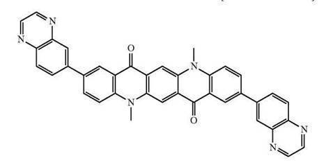
これらの欠点を解決するため、近年、有機光電変換膜を信号読み出し用基板上に配置した構造を有する光電変換素子の開発が進んでいる。このような有機光電変換膜を使用した光電変換素子として、例えば、特許文献1では、以下のような化合物を含む光電変換膜を有する光電変換素子が開示されている。
例えば、応答性のより一層の向上が求められている。
また、光電変換素子においては、所定の加熱処理が施された後でも、加熱処理前と同様に優れた特性を維持することが求められており、特に、加熱処理後においても応答性が低減しないことが求められている。つまり、光電変換素子の耐熱性の向上が求められている。
本発明者は、特許文献1で具体的に開示されている化合物(例えば、上述した化合物)を用いて光電変換素子を作製し、得られた光電変換素子の応答性、および、耐熱性(加熱処理後の応答性)について検討したところ、その特性は必ずしも昨今求められるレベルに達しておらず、さらなる向上が必要であることを見出した。
また、本発明は、光電変換素子を含む撮像素子および光センサを提供することも目的とする。さらに、本発明は、上記光電変換素子に適用される化合物を提供することも目的とする。
すなわち、以下に示す手段により上記課題を解決し得る。
光電変換膜が、後述する式(1)で表され、分子量が400~1200である化合物を含む、光電変換素子。
(2) 式(1)中、B1およびB2が、それぞれ独立に、アルキル基、アリール基、および、ヘテロアリール基のいずれかを表す、(1)に記載の光電変換素子。
(3) 式(1)中、A1およびA2の両方が、後述する式(1f)~(1h)で表される置換基のいずれかを表す、(1)または(2)に記載の光電変換素子。
(4) 式(1)中、A1およびA2の両方が、後述する式(1a)~(1e)、および、式(1i)で表される置換基のいずれかを表す、(1)~(3)のいずれかに記載の光電変換素子。
(5) 式(1)中、A1およびA2の両方が、式(1a)で表される置換基、式(1b)で表される置換基、式(1e)で表される置換基、および、式(1i)で表される置換基のいずれかを表す、(4)に記載の光電変換素子。
(6) 式(1)中、A1およびA2の両方が、式(1a)で表される置換基、式(1b)で表される置換基、および、式(1i)で表される置換基のいずれかを表す、(4)または(5)に記載の光電変換素子。
(7) 式(1)中、A1およびA2の両方が、同じ基を表す、(1)~(6)のいずれかに記載の光電変換素子。
(8) 式(1)で表される化合物の分子量が、470~900である、(1)~(7)のいずれかに記載の光電変換素子。
(9) 光電変換膜が、さらにn型有機半導体を含む、(1)~(8)のいずれかに記載の光電変換素子。
(10) 光電変換膜が、さらにp型有機半導体を含む、(1)~(8)のいずれかに記載の光電変換素子。
(11) さらに、電子ブロッキング膜を有する、(1)~(10)のいずれかに記載の光電変換素子。
(12) さらに、正孔ブロッキング膜を有する、(1)~(11)のいずれかに記載の光電変換素子。
(13) (1)~(12)のいずれかに記載の光電変換素子を含む光センサ。
(14) (1)~(12)のいずれかに記載の光電変換素子を含む撮像素子。
(15) 式(1)で表される化合物。

式(1)中、R1~R8は、それぞれ独立に、水素原子または置換基を表す。B1およびB2は、それぞれ独立に、水素原子または置換基を表す。A1およびA2は、それぞれ独立に、水素原子または置換基を表し、A1およびA2の少なくとも一方は、式(1a)~(1e)、および、式(1i)で表される置換基のいずれかを表す。また、R1~R8、A1、A2、B1およびB2のうち隣り合う基同士は、連結して環を形成してもよい。

式(1a)中、Ra1~Ra5は、それぞれ独立に、水素原子、アルキル基、アリール基、ヘテロアリール基、アルコキシ基、アルキルチオ基、エチニル基、エテニル基、アシル基、ハロゲン原子、または、シリル基を表し、Ra1~Ra5のうち少なくとも1つはフッ素原子、塩素原子、臭素原子、フルオロアルキル基、および、シリル基のいずれかを表す。*は結合位置を表す。

式(1b)中、Rb1~Rb7は、それぞれ独立に、水素原子または置換基を表す。*は結合位置を表す。また、Rb1~Rb7のうち隣り合う基同士は、連結して環を形成してもよい。

式(1c)中、Rc1およびRc2は、それぞれ独立に、水素原子または置換基を表す。Rc1とRc2とは互いに連結して環を形成してもよい。YC1は、硫黄原子、酸素原子、セレン原子、NRc3、または、CRc4Rc5を表す。Rc3~Rc5は、それぞれ独立に、水素原子または置換基を表す。*は結合位置を表す。

式(1d)中、Rd1~Rd3は、それぞれ独立に、水素原子または置換基を表す。Yd1は、硫黄原子、酸素原子、セレン原子、NRd4、または、CRd5Rd6を表す。Zd1は、硫黄原子、酸素原子、セレン原子、NRd7、CRd8Rd9、または、Rd10C=CRd11を表す。Rd4~Rd11は、それぞれ独立に、水素原子または置換基を表す。*は結合位置を表す。Rd1とRd2、Rd2とRd10またはRd2とRd11は、互いに連結して環を形成してもよい。
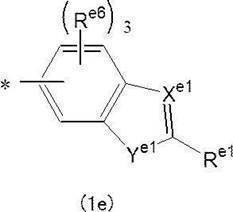
式(1e)中、Xe1は、窒素原子またはCRe2を表す。Ye1は、硫黄原子、酸素原子、セレン原子、NRe3、または、CRe4Re5を表す。Re1~Re6は、それぞれ独立に、水素原子または置換基を表す。Re1とRe2とは互いに連結して環を形成してもよい。*は結合位置を表す。

式(1i)中、Ri1およびRi2は、それぞれ独立に、水素原子、アルキル基、アリール基、または、ヘテロアリール基を表す。Yi1は、酸素原子、セレン原子、NRi3、または、CRi4Ri5を表す。Ri3~Ri5は、それぞれ独立に、水素原子または置換基を表す。*は結合位置を表す。
また、本発明によれば、光電変換素子を含む撮像素子および光センサを提供することもできる。さらに、本発明によれば、上記光電変換素子に適用される化合物を提供することもできる。
なお、本明細書において置換または無置換を明記していない置換基等については、目的とする効果を損なわない範囲で、その基にさらに置換基(好ましくは、後述する置換基W)が置換していてもよい。例えば、「アルキル基」という表記は、置換基(好ましくは、置換基W)が置換していてもよいアルキル基に該当する。
また、本明細書において「~」を用いて表される数値範囲は、「~」の前後に記載される数値を下限値および上限値として含む範囲を意味する。
図1Aに示す光電変換素子10aは、下部電極として機能する導電性膜(以下、下部電極とも記す)11と、電子ブロッキング膜16Aと、後述する式(1)で表される化合物を含む光電変換膜12と、上部電極として機能する透明導電性膜(以下、上部電極とも記す)15とがこの順に積層された構成を有する。
図1Bに別の光電変換素子の構成例を示す。図1Bに示す光電変換素子10bは、下部電極11上に、電子ブロッキング膜16Aと、光電変換膜12と、正孔ブロッキング膜16Bと、上部電極15とがこの順に積層された構成を有する。なお、図1Aおよび図1B中の電子ブロッキング膜16A、光電変換膜12、および、正孔ブロッキング膜16Bの積層順は、用途および特性に応じて、適宜変更してもよい。
また、光電変換素子10a(または、10b)を使用する場合には、電圧を印加することができる。この場合、下部電極11と上部電極15とが一対の電極をなし、この一対の電極間に、1×10⁻⁵~1×10⁷V/cmの電圧を印加することが好ましい。性能および消費電力の観点から、1×10-4~1×107V/cmの電圧がより好ましく、1×10-3~5×106V/cmの電圧がさらに好ましい。
なお、電圧印加方法については、図1Aおよび図1Bにおいて、電子ブロッキング膜16A側が陰極となり、光電変換膜12側が陽極となるように印加することが好ましい。光電変換素子10a(または、10b)を光センサとして使用した場合、また、撮像素子に組み込んだ場合も、同様の方法により電圧を印加できる。
後段で、詳述するように、光電変換素子10a(または、10b)は撮像素子用途、および、光センサ用途に好適に適用できる。
図2に示される光電変換素子200は、有機光電変換膜209と無機光電変換膜201とを備えるハイブリッド型の光電変換素子である。なお、有機光電変換膜209には、後述する式(1)で表される化合物が含まれる。
無機光電変換膜201は,p型シリコン基板205上に、n型ウェル202、p型ウェル203、および、n型ウェル204を有する。
p型ウェル203とn型ウェル204との間に形成されるpn接合にて青色光が光電変換され(B画素)、p型ウェル203とn型ウェル202との間に形成されるpn接合にて赤色光が光電変換される(R画素)。なお、n型ウェル202、p型ウェル203、およびn型ウェル204の導電型は、これらに限らない。
絶縁層207の上には、画素毎に区分けした透明な画素電極208が配置される。その上に、緑色光を吸収して光電変換する有機光電変換膜209が各画素共通に一枚構成で配置される。その上に、電子ブロッキング膜212が各画素共通に一枚構成で配置される。その上に、一枚構成の透明な共通電極210が配置される。最上層に、透明な保護膜211が配置されている。電子ブロッキング膜212と有機光電変換膜209との積層順は図2とは逆であってもよく、共通電極210は、画素毎に区分けして配置されてもよい。
有機光電変換膜209は、緑色光を検出するG画素を構成する。
(式(1)で表される化合物)
光電変換膜12(または、有機光電変換膜209)は、光電変換材料として式(1)で表される化合物を含む膜である。この化合物を使用することにより、優れた応答性および耐熱性を示す、光電変換素子が得られる。
以下、式(1)で表される化合物について詳述する。

なお、R1~R8、A1、A2、B1およびB2のうち隣り合う基同士は、連結して環を形成してもよい。形成される環の種類は特に制限されず、芳香環であっても、非芳香環であってもよく、芳香環であることが好ましい。また、環は、単環であっても、2つ以上の環からなる縮環であってもよい。また、芳香環は、芳香族炭化水素環であっても、芳香族複素環であってもよい。
なかでも、本発明の効果がより優れる点で、B1およびB2は、それぞれ独立に、アルキル基、アリール基、または、ヘテロアリール基であることが好ましく、B1およびB2の両方がアルキル基であることがより好ましい。
また、B1およびB2が、同じ基であることが好ましい。例えば、B1およびB2が共に、メチル基を示す場合が挙げられる。
アルキル基としては、例えば、メチル基、エチル基、n-プロピル基、i-プロピル基、n-ブチル基、n-ヘキシル基、および、シクロへキシル基等が挙げられる。
アリール基としては、例えば、フェニル基、ナフチル基、アントリル基、ピレニル基、フェナントレニル基、メチルフェニル基、ジメチルフェニル基、ビフェニル基、および、フルオレニル基等が挙げられ、フェニル基、ナフチル基、または、アントリル基が好ましい。
ヘテロアリール基には、炭素原子および水素原子以外にヘテロ原子が含まれる。ヘテロ原子としては、例えば、窒素原子、硫黄原子、酸素原子、セレン原子、テルル原子、リン原子、ケイ素原子、および、ホウ素原子が挙げられ、窒素原子、硫黄原子、または、酸素原子が好ましい。
ヘテロアリール基に含まれるヘテロ原子の数は特に制限されず、通常、1~10個程度であり、1~4個が好ましく、1~2個がより好ましい。
ヘテロアリール基の環員数は特に制限されず、3~8員環が好ましく、5~7員環がより好ましく、5~6員環がさらに好ましい。なお、ヘテロアリール基は、単環構造であっても、2つ以上の環が縮環した縮環構造であってもよい。縮環構造の場合、ヘテロ原子を含まない芳香族炭化水素環(例えば、ベンゼン環)が含まれていてもよい。
ヘテロアリール基としては、例えば、ピリジル基、キノリル基、イソキノリル基、アクリジニル基、フェナントリジニル基、プテリジニル基、ピラジニル基、キノキサリニル基、ピリミジニル基、キナゾリル基、ピリダジニル基、シンノリニル基、フタラジニル基、トリアジニル基、オキサゾリル基、ベンゾオキサゾリル基、チアゾリル基、ベンゾチアゾリル基、イミダゾリル基、ベンゾイミダゾリル基、ピラゾリル基、インダゾリル基、イソオキサゾリル基、ベンゾイソオキサゾリル基、イソチアゾリル基、ベンゾイソチアゾリル基、オキサジアゾリル基、チアジアゾリル基、トリアゾリル基、テトラゾリル基、フリル基、ベンゾフリル基、チエニル基、ベンゾチエニル基、ジベンゾフリル基、ジベンゾチエニル基、ピロリル基、インドリル基、イミダゾピリジニル基、および、カルバゾリル基等が挙げられる。
なかでも、本発明の効果がより優れる点で、A1およびA2の両方が、式(1f)~(1h)で表される置換基のいずれかを表すことが好ましい。
また、本発明の効果がより優れる点で、A1およびA2の両方が、同じ基を表すことが好ましい。例えば、A1およびA2の両方が、Rf1~Rf5が全て水素原子である式(1f)で表される基を表す場合が挙げられる。
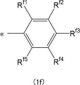
なお、上記各基は、さらに置換基を有していてもよい。例えば、アルキル基は、フルオロアルキル基であってもよい。つまり、上記アルキル基は、フッ素原子が置換してもよいアルキル基である。
フルオロアルキル基とは、アルキル基中の少なくとも1つの水素原子がフッ素原子に置換された基であり、アルキル基中の全ての水素原子がフッ素原子に置換された基であることが好ましい。フルオロアルキル基中の炭素数は特に制限されず、本発明の効果がより優れる点で、1~10が好ましく、1~6がより好ましく、1~3がさらに好ましく、1が特に好ましい。フルオロアルキル基としては、直鎖状、分岐鎖状、および、環状のいずれであってもよい。
シリル基とは、-Si(Rx)3(Rxは、水素原子または置換基を表し、3つのRxは同じでも異なっていてもよい。)で表される基である。上記置換基の定義は、後述する置換基Wと同義である。Rxとしては、アルキル基、または、アリール基が好ましい。アルキル基中の炭素数は特に制限されず、1~3が好ましい。

Yg1は、硫黄原子、酸素原子、セレン原子、NRg4、CRg5Rg6、またはRg7C=CRg8を表す。
Rg1~Rg8は、それぞれ独立に、水素原子または置換基を表す。置換基の定義は、後述する置換基Wと同義である。
*は結合位置を表す。
また、Rg1~Rg8のうち隣り合う基同士は、連結して環を形成してもよい。Rg1~Rg8のうち隣り合う基同士が連結して形成される環としては、芳香環であっても、非芳香環であってもよい。また、環は、単環であっても、2つ以上の環からなる縮環であってもよい。また、芳香環は、芳香族炭化水素環であっても、芳香族複素環であってもよい。なかでも、本発明の効果がより優れる点で、Rg1~Rg8のうち隣り合う基同士が連結して形成される環としては、芳香環が好ましく、芳香族炭化水素環がより好ましく、ベンゼン環がさらに好ましい。Rg1~Rg8のうち隣り合う基同士が連結して形成される環には、置換基が置換していてもよい。置換基の定義は、後述する置換基Wと同義である。
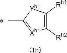
Yh1は、硫黄原子、酸素原子、セレン原子、NRh4、または、CRh5Rh6を表す。
Rh1~Rh6は、それぞれ独立に、水素原子または置換基を表す。置換基の定義は、後述する置換基Wと同義である。
*は結合位置を表す。
また、Rh1~Rh6のうち隣り合う基同士は、連結して環を形成してもよい。Rh1~Rh6のうち隣り合う基同士が連結して形成される環としては、芳香環であっても、非芳香環であってもよい。また、環は、単環であっても、2つ以上の環からなる縮環であってもよい。また、芳香環は、芳香族炭化水素環であっても、芳香族複素環であってもよい。なかでも、本発明の効果がより優れる点で、Rh1~Rh6のうち隣り合う基同士が連結して形成される環としては、芳香環が好ましく、芳香族炭化水素環がより好ましく、ベンゼン環がさらに好ましい。Rg1~Rg8のうち隣り合う基同士が連結して形成される環には、置換基が置換していてもよい。置換基の定義は、後述する置換基Wと同義である。
また、上記式(1g)で表される置換基の好適態様としては、式(1b)で表される置換基、および、式(1e)で表される置換基が挙げられる。
さらに、上記式(1h)で表される置換基の好適態様としては、式(1c)で表される置換基、式(1d)で表される置換基、および、式(1i)で表される置換基が挙げられる。
なかでも、本発明の効果がより優れる点で、A1およびA2は、式(1a)で表される置換基、式(1b)で表される置換基、式(1e)で表される置換基、および、式(1i)で表される置換基のいずれかを表すことが好ましく、式(1a)で表される置換基、および、式(1b)で表される置換基、および、式(1i)で表される置換基のいずれかを表すことがより好ましい。
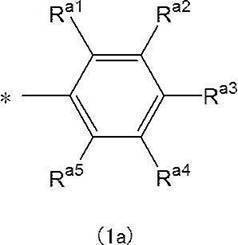
また、本発明の効果がより優れる点で、Ra1~Ra5のうち1~2つがフッ素原子、塩素原子、臭素原子、フルオロアルキル基、および、シリル基のいずれかを表すことが好ましい。
なかでも、本発明の効果がより優れる点で、Ra1~Ra5のうち少なくとも1つが、フッ素原子またはフルオロアルキル基であることが好ましい。
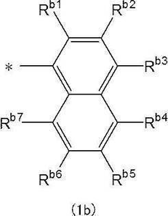
また、Rb1~Rb7のうち隣り合う基同士は、連結して環を形成してもよい。
Rb1~Rb7のうち隣り合う基同士が連結して形成される環としては、芳香環であっても、非芳香環であってもよい。また、環は、単環であっても、2つ以上の環からなる縮環であってもよい。また、芳香環は、芳香族炭化水素環であっても、芳香族複素環であってもよい。なかでも、本発明の効果がより優れる点で、Rb1~Rb7のうち隣り合う基同士が連結して形成される環としては、芳香環が好ましく、芳香族炭化水素環がより好ましく、ベンゼン環がさらに好ましい。
なかでも、本発明の効果がより優れる点で、Rb1~Rb7は水素原子であることが好ましい。

Rc1とRc2とが互いに連結して形成される環としては、芳香環であっても、非芳香環であってもよい。また、環は、単環であっても、2つ以上の環からなる縮環であってもよい。また、芳香環は、芳香族炭化水素環であっても、芳香族複素環であってもよい。なかでも、本発明の効果がより優れる点で、Rc1とRc2とが互いに連結して形成される環としては、芳香環が好ましく、芳香族炭化水素環がより好ましく、ベンゼン環がさらに好ましい。
YC1は、硫黄原子、酸素原子、セレン原子、NRc3、または、CRc4Rc5を表す。Rc3~Rc5は、それぞれ独立に、水素原子または置換基を表す。上記置換基の定義は、後述する置換基Wと同義である。
*は結合位置を表す。
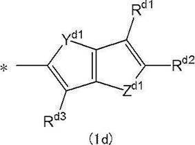
上記置換基の定義は、後述する置換基Wと同義である。
Yd1は、硫黄原子、酸素原子、セレン原子、NRd4、または、CRd5Rd6を表す。
Zd1は、硫黄原子、酸素原子、セレン原子、NRd7、CRd8Rd9、または、Rd10C=CRd11を表す。
Rd4~Rd11は、それぞれ独立に、水素原子または置換基を表す。上記置換基の定義は、後述する置換基Wと同義である。
なお、Rd1とRd2、Rd2とRd10またはRd2とRd11は、互いに連結して環を形成してもよい。Rd1とRd2、Rd2とRd10またはRd2とRd11が互いに連結して形成される環としては、芳香環であっても、非芳香環であってもよい。また、環は、単環であっても、2つ以上の環からなる縮環であってもよい。また、芳香環は、芳香族炭化水素環であっても、芳香族複素環であってもよい。なかでも、本発明の効果がより優れる点で、Rd1とRd2、Rd2とRd10またはRd2とRd11が互いに連結して形成される環としては、芳香環が好ましく、芳香族炭化水素環がより好ましく、ベンゼン環がさらに好ましい。
*は結合位置を表す。

Xe1がCRe2を表す場合、Re1とRe2とは互いに連結して環を形成してもよい。
Re1とRe2とが互いに連結して形成される環としては、芳香環であっても、非芳香環であってもよい。また、環は、単環であっても、2つ以上の環からなる縮環であってもよい。また、芳香環は、芳香族炭化水素環であっても、芳香族複素環であってもよい。なかでも、本発明の効果がより優れる点で、Re1とRe2とが互いに連結して形成される環としては、芳香環が好ましく、芳香族炭化水素環がより好ましく、ベンゼン環がさらに好ましい。
*は結合位置を表す。
なお、式(1e)中の*を含む結合手は、ベンゼン環上の置換可能ないずれの位置にあってもよい。つまり、*を含む結合手は、以下の構造式で示されるように、*1~*4のいずれかの位置にあり、それ以外の*1~*4のいずれか3つにはRe6が結合している。


Yi1は、硫黄原子、酸素原子、セレン原子、NRi3、または、CRi4Ri5を表す。Ri3~Ri5は、それぞれ独立に、水素原子または置換基を表す。上記置換基の定義は、後述する置換基Wと同義である。
*は結合位置を表す。
置換基Wとしては、例えば、ハロゲン原子、アルキル基(シクロアルキル基、ビシクロアルキル基、および、トリシクロアルキル基を含む)、アルケニル基(シクロアルケニル基、および、ビシクロアルケニル基を含む)、アルキニル基、アリール基、複素環基(ヘテロ環基といってもよい)、シアノ基、ヒドロキシ基、ニトロ基、カルボキシ基、アルコキシ基、アリールオキシ基、シリルオキシ基、ヘテロ環オキシ基、アシルオキシ基、カルバモイルオキシ基、アルコキシカルボニルオキシ基、アリールオキシカルボニルオキシ基、アミノ基(アニリノ基を含む)、アンモニオ基、アシルアミノ基、アミノカルボニルアミノ基、アルコキシカルボニルアミノ基、アリールオキシカルボニルアミノ基、スルファモイルアミノ基、アルキルまたはアリールスルホニルアミノ基、メルカプト基、アルキルチオ基、アリールチオ基、ヘテロ環チオ基、スルファモイル基、スルホ基、アルキルまたはアリールスルフィニル基、アルキルまたはアリールスルホニル基、アシル基、アリールオキシカルボニル基、アルコキシカルボニル基、カルバモイル基、アリールまたはヘテロ環アゾ基、イミド基、ホスフィノ基、ホスフィニル基、ホスフィニルオキシ基、ホスフィニルアミノ基、ホスホノ基、シリル基、ヒドラジノ基、ウレイド基、ボロン酸基(-B(OH)2)、ホスファト基(-OPO(OH)2)、スルファト基(-OSO3H)、および、その他の公知の置換基が挙げられる。
また、置換基Wは、さらに置換基Wで置換されていてもよい。例えば、アルキル基にハロゲン原子が置換していてもよい。
なお、置換基Wの詳細については、特開2007-234651号公報の段落[0023]に記載される。
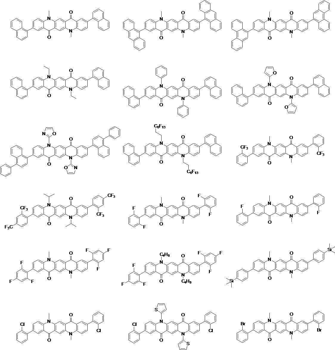

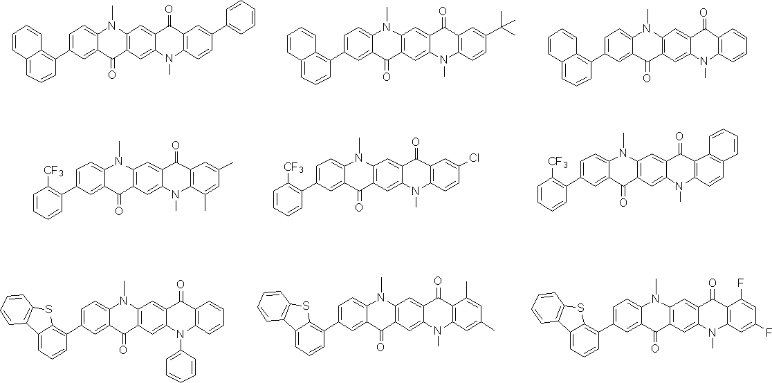
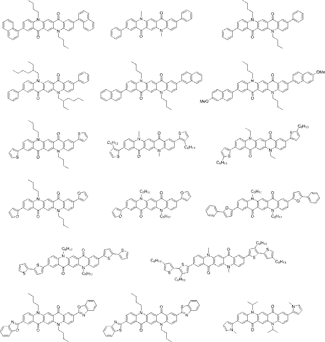

光電変換膜には、上述した式(1)で表される化合物以外の他の成分が含まれていてもよい。例えば、光電変換膜には、n型有機半導体またはp型有機半導体が含まれていてもよい。
n型有機半導体とは、アクセプタ性有機半導体材料(化合物)であり、電子を受容しやすい性質がある有機化合物をいう。さらに詳しくは、n型有機半導体とは、2つの有機化合物を接触させて用いたときに電子親和力の大きい方の有機化合物をいう。
n型有機半導体としては、例えば、縮合芳香族炭素環化合物(例えば、ナフタレン誘導体、アントラセン誘導体、フェナントレン誘導体、テトラセン誘導体、ピレン誘導体、ペリレン誘導体、および、フルオランテン誘導体)、窒素原子、酸素原子、および、硫黄原子の少なくとも1つを含有する5~7員のヘテロ環化合物(例えば、ピリジン、ピラジン、ピリミジン、ピリダジン、トリアジン、キノリン、キノキサリン、キナゾリン、フタラジン、シンノリン、イソキノリン、プテリジン、アクリジン、フェナジン、フェナントロリン、テトラゾール、ピラゾール、イミダゾール、および、チアゾール等)、ポリアリーレン化合物、フルオレン化合物、シクロペンタジエン化合物、シリル化合物、ならびに、含窒素ヘテロ環化合物を配位子として有する金属錯体等が挙げられる。
p型有機半導体としては、例えば、トリアリールアミン化合物、ベンジジン化合物、ピラゾリン化合物、スチリルアミン化合物、ヒドラゾン化合物、カルバゾール化合物、ポリシラン化合物、チオフェン化合物、シアニン化合物、オキソノール化合物、ポリアミン化合物、インドール化合物、ピロール化合物、ピラゾール化合物、ポリアリーレン化合物、縮合芳香族炭素環化合物、および、含窒素ヘテロ環化合物を配位子として有する金属錯体等が挙げられる。
光電変換膜は、主に、乾式成膜法により成膜できる。乾式成膜法の具体例としては、蒸着法(特に、真空蒸着法)、スパッタリング法、イオンプレーティング法、および、MBE(Molecular Beam Epitaxy)法等の物理気相成長法、または、プラズマ重合等のCVD(Chemical Vapor Deposition)法が挙げられる。なかでも、真空蒸着法が好ましい。真空蒸着法により光電変換膜を成膜する場合、真空度および蒸着温度等の製造条件は常法に従って設定することができる。
電極(上部電極(透明導電性膜)15と下部電極(導電性膜)11)は、導電性材料から構成される。導電性材料としては、金属、合金、金属酸化物、電気伝導性化合物、および、これらの混合物等が挙げられる。
上部電極15から光が入射されるため、上部電極15は検知したい光に対し透明であることが好ましい。上部電極15を構成する材料としては、例えば、アンチモンまたはフッ素等をドープした酸化錫(ATO、FTO)、酸化錫、酸化亜鉛、酸化インジウム、酸化インジウム錫(ITO)、および、酸化亜鉛インジウム(IZO)等の導電性金属酸化物、金、銀、クロム、および、ニッケル等の金属薄膜、これらの金属と導電性金属酸化物との混合物または積層物、ならびに、ポリアニリン、ポリチオフェン、および、ポリピロール等の有機導電性材料等が挙げられる。なかでも、高導電性および透明性等の点から、導電性金属酸化物が好ましい。
電極の材料がITOの場合、電子ビーム法、スパッタリング法、抵抗加熱蒸着法、化学反応法(ゾル-ゲル法等)、および、酸化インジウムスズの分散物の塗布等の方法が挙げられる。
本発明の光電変換素子は、電荷ブロッキング膜を有していてもよい。この膜を有することにより、得られる光電変換素子の特性(光電変換効率および応答速度等)がより優れる。電荷ブロッキング膜としては、電子ブロッキング膜と正孔ブロッキング膜とが挙げられる。以下に、それぞれの膜について詳述する。
電子ブロッキング膜には、電子供与性化合物が含まれる。具体的には、低分子材料では、N,N’-ビス(3-メチルフェニル)-(1,1’-ビフェニル)-4,4’-ジアミン(TPD)、および、4,4’-ビス[N-(ナフチル)-N-フェニル-アミノ]ビフェニル(α-NPD)等の芳香族ジアミン化合物、ポルフィリン、テトラフェニルポルフィリン銅、フタロシアニン、銅フタロシアニン、および、チタニウムフタロシアニンオキサイド等のポルフィリン化合物、オキサゾール、オキサジアゾール、トリアゾール、イミダゾール、イミダゾロン、スチルベン誘導体、ピラゾリン誘導体、テトラヒドロイミダゾール、ポリアリールアルカン、ブタジエン、4,4’,4’’-トリス(N-(3-メチルフェニル)N-フェニルアミノ)トリフェニルアミン(m-MTDATA)、トリアゾール誘導体、オキサジザゾール誘導体、イミダゾール誘導体、ポリアリールアルカン誘導体、ピラゾリン誘導体、ピラゾロン誘導体、フェニレンジアミン誘導体、アリールアミン誘導体、アミノ置換カルコン誘導体、オキサゾール誘導体、スチリルアントラセン誘導体、フルオレノン誘導体、ヒドラゾン誘導体、ならびに、シラザン誘導体等が挙げられ、高分子材料では、フェニレンビニレン、フルオレン、カルバゾール、インドール、ピレン、ピロール、ピコリン、チオフェン、アセチレン、および、ジアセチレン等の重合体、または、その誘導体が挙げられる。
電子ブロッキング膜は、無機材料で構成されていてもよい。一般的に、無機材料は有機材料よりも誘電率が大きいため、無機材料を電子ブロッキング膜に用いた場合に、光電変換膜に電圧が多くかかるようになり、光電変換効率が高くなる。電子ブロッキング膜となりうる無機材料としては、例えば、酸化カルシウム、酸化クロム、酸化クロム銅、酸化マンガン、酸化コバルト、酸化ニッケル、酸化銅、酸化ガリウム銅、酸化ストロンチウム銅、酸化ニオブ、酸化モリブデン、酸化インジウム銅、酸化インジウム銀、および、酸化イリジウム等が挙げられる。
正孔ブロッキング膜には、電子受容性化合物が含まれる。
電子受容性化合物としては、1,3-ビス(4-tert-ブチルフェニル-1,3,4-オキサジアゾリル)フェニレン(OXD-7)等のオキサジアゾール誘導体、アントラキノジメタン誘導体、ジフェニルキノン誘導体、バソクプロイン、バソフェナントロリン、およびこれらの誘導体、トリアゾール化合物、トリス(8-ヒドロキシキノリナート)アルミニウム錯体、ビス(4-メチル-8-キノリナート)アルミニウム錯体、ジスチリルアリーレン誘導体、ならびに、シロール化合物等が挙げられる。
光電変換素子は、さらに基板を含んでいてもよい。使用される基板の種類は特に制限されず、半導体基板、ガラス基板、および、プラスチック基板が挙げられる。
なお、基板の位置は特に制限されず、通常、基板上に導電性膜、光電変換膜、および透明導電性膜をこの順で積層する。
光電変換素子は、さらに封止層を含んでいてもよい。光電変換材料は水分子等の劣化因子の存在で顕著にその性能が劣化することがある。そこで、水分子を浸透させない緻密な金属酸化物、金属窒化物、および、金属窒化酸化物等のセラミックス、または、ダイヤモンド状炭素(DLC)等の封止層で光電変換膜全体を被覆して封止することで、上記劣化を防止できる。
なお、封止層としては、特開2011-082508号公報の段落[0210]~[0215]に記載に従って、材料の選択および製造を行ってもよい。
光電変換素子の用途として、例えば、光電池および光センサが挙げられ、本発明の光電変換素子は光センサとして用いることが好ましい。光センサとしては、上記光電変換素子単独で用いてもよいし、上記光電変換素子を直線状に配したラインセンサ、または、平面上に配した2次元センサとして用いてもよい。本発明の光電変換素子は、ラインセンサでは、スキャナー等の様に光学系および駆動部を用いて光画像情報を電気信号に変換し、2次元センサでは、撮像モジュールのように光画像情報を光学系でセンサ上に結像させ電気信号に変換することで撮像素子として機能する。
次に、光電変換素子10aを備えた撮像素子の構成例を説明する。
なお、以下に説明する構成例において、すでに説明した部材等と同等な構成または作用を有する部材等については、図中に同一符号または相当符号を付すことにより、説明を簡略化または省略する。
撮像素子とは画像の光情報を電気信号に変換する素子であり、複数の光電変換素子が同一平面状でマトリクス上に配置されており、各々の光電変換素子(画素)において光信号を電気信号に変換し、その電気信号を画素ごとに逐次撮像素子外に出力できるものをいう。そのために、画素ひとつあたり、一つの光電変換素子、一つ以上のトランジスタから構成される。
図3は、本発明の一実施形態を説明するための撮像素子の概略構成を示す断面模式図である。この撮像素子は、デジタルカメラおよびデジタルビデオカメラ等の撮像装置、ならびに、電子内視鏡および携帯電話機等の撮像モジュール等に搭載される。
この撮像素子は、図1Aに示したような構成の複数の光電変換素子と、各光電変換素子の光電変換膜で発生した電荷に応じた信号を読み出す読み出し回路が形成された回路基板とを有し、回路基板上方の同一面上に、複数の光電変換素子が一次元状または二次元状に配列された構成となっている。
対向電極電圧供給部115と読み出し回路116が形成された回路基板上に、接続部105および106、複数の接続電極103、複数の画素電極104、ならびに、絶縁層102を形成する。複数の画素電極104は、絶縁層102の表面に例えば正方格子状に配置する。
化合物(D-1)は、以下のスキームに従って、合成した。
1H NMRスペクトル(400MHz、CDCl3)を図4に示す。
MS(ESI+)m/z:621.3([M+H]+)
なお、化合物(D-7)、(D-8)、(D-10)~(D-13)の1H NMR(溶媒:CDCl3)スペクトルをそれぞれ図5~図10に記載する。
また、比較化合物に該当する化合物(R-1)は、Luminescence Technology社より購入した。
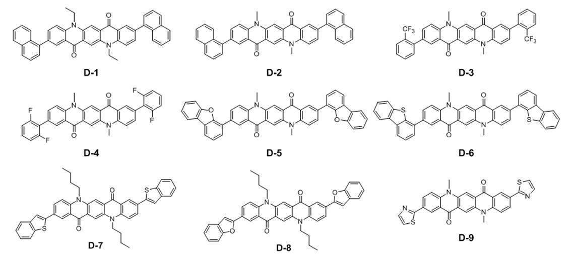

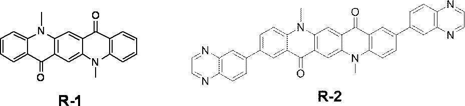
得られた化合物を用いて図1Aの形態の光電変換素子を作製した。以下では、化合物(D-1)を用いた場合について詳述する。
具体的には、ガラス基板上に、アモルファス性ITOをスパッタ法により成膜して、下部電極11(厚み:30nm)を形成した。さらに下部電極11上に酸化モリブデン(MoOX)を真空蒸着法により成膜して、電子ブロッキング膜16Aとして酸化モリブデン層(厚み:60nm)を形成した。
さらに、基板の温度を25℃に制御した状態で、酸化モリブデン層上に化合物(D-1)と下記化合物(N-1)とをそれぞれ単層換算で50nm、50nmとなるように共蒸着して成膜し、100nmのバルクヘテロ構造を有する光電変換膜12を形成した。
さらに、光電変換膜12上に、アモルファス性ITOをスパッタ法により成膜して、上部電極15(透明導電性膜)(厚み:10nm)を形成した。上部電極15上に、加熱蒸着により封止層としてSiO膜を形成した後、その上にALCVD(Atomic Layer Chemical Vapor Deposition)法により酸化アルミニウム(Al2O3)層を形成し、光電変換素子を作製した。

(応答性の評価)
得られた光電変換素子を用いて、以下の応答性の評価を実施した。
具体的には、光電変換素子に1.0×10⁵V/cmの強度となるように電圧を印加した。その後、LED(light emitting diode)を瞬間的に点灯させて上部電極(透明導電性膜)側から光を照射し、そのときの光電流をオシロスコープで測定して、0から97%信号強度までの立ち上がり時間を計った。そして比較例1の立ち上がり時間を10としたときの相対値を求めた。結果を表1に示す。
なお、立ち上がり時間の相対値が比較例1に対して、3未満の場合を「A」、3以上5未満の場合を「B」、5以上10未満の場合を「C」、10以上の場合を「D」とした。実用上、「A」または「B」であることが好ましく、「A」であることがより好ましい。
得られた光電変換素子を用いて、以下の耐熱性の評価を実施した。
窒素雰囲気下、暗所にて作製した各光電変換素子を150℃で10分間加熱して、加熱処理後の応答速度を測定した。具体的には、光電変換素子に1×10⁵V/cmの強度となるように電圧を印加した。その後、LED(light emitting diode)を瞬間的に点灯させて上部電極(透明導電性膜)側から光を照射し、そのときの光電流をオシロスコープで測定して、0から97%信号強度までの立ち上がり時間を計った。そして各試料の加熱前の光電変換素子の立ち上がり時間を1としたときの相対値を求めた。結果を表1に示す。
なお、加熱後の立ち上がり時間の相対値が、1.5未満の場合を「A」、1.5以上2.0未満の場合を「B」、2.0以上の場合を「C」とした。実用上、「A」または「B」であることが好ましく、「A」であることがより好ましい。
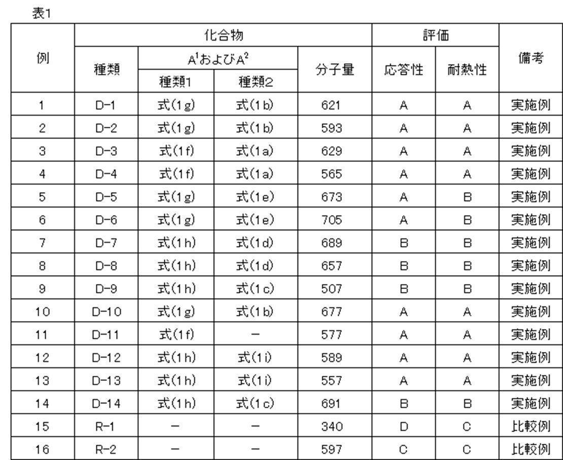
なかでも、A1およびA2の両方が、式(1a)で表される置換基、式(1b)で表される置換基、式(1e)で表される置換基、および、式(1i)で表される置換基のいずれかを表す場合により効果が優れ、A1およびA2の両方が、式(1a)で表される置換基、式(1b)で表される置換基、および、式(1i)で表される置換基のいずれかを表す場合にさらに効果が優れることが確認された。
なお、所定の化合物を用いていない比較例1および2では、所望の効果は得られなかった。なお、比較例2で用いられた化合物は、特許文献1で具体的に開示されている化合物に該当する。
図3に示す形態と同様の撮像素子を作製した。すなわち、CMOS基板上に、アモルファス性TiN 30nmをスパッタ法により成膜後、フォトリソグラフィーによりCMOS基板上のフォトダイオード(PD)の上にそれぞれ1つずつ画素が存在するようにパターニングして下部電極とし、電子ブロッキング材料の成膜以降は例1~14と同様に作製した。得られた撮像素子での応答性評価および耐熱性評価も同様に行い、表1と同様な結果が得られ、撮像素子においても優れた性能を示すことが分かった。
11 導電性膜(下部電極)
12 光電変換膜
15 透明導電性膜(上部電極)
16A 電子ブロッキング膜
16B 正孔ブロッキング膜
100 画素分離型撮像素子
101 基板
102 絶縁層
103 接続電極
104 画素電極(下部電極)
105 接続部
106 接続部
107 光電変換膜
108 対向電極(上部電極)
109 緩衝層
110 封止層
111 カラーフィルタ(CF)
112 隔壁
113 遮光層
114 保護層
115 対向電極電圧供給部
116 読み出し回路
200 光電変換素子(ハイブリッド型の光電変換素子)
201 無機光電変換膜
202 n型ウェル
203 p型ウェル
204 n型ウェル
205 p型シリコン基板
207 絶縁層
208 画素電極
209 有機光電変換膜
210 共通電極
211 保護膜
212 電子ブロッキング膜
Claims (15)
- 導電性膜、光電変換膜、および、透明導電性膜をこの順で有する光電変換素子であって、
前記光電変換膜が、式(1)で表され、分子量が400~1200である化合物を含む、光電変換素子。

式(1)中、R1~R8は、それぞれ独立に、水素原子または置換基を表す。B1およびB2は、それぞれ独立に、水素原子または置換基を表す。A1およびA2は、それぞれ独立に、水素原子または置換基を表し、A1およびA2の少なくとも一方は、式(1f)~(1h)で表される置換基のいずれかを表す。また、R1~R8、A1、A2、B1およびB2のうち隣り合う基同士は、連結して環を形成してもよい。
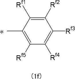
式(1f)中、Rf1~Rf5は、それぞれ独立に、水素原子、アルキル基、アリール基、ヘテロアリール基、アルコキシ基、アルキルチオ基、エチニル基、エテニル基、アシル基、ハロゲン原子、または、シリル基を表す。*は結合位置を表す。

式(1g)中、Xg1は、窒素原子またはCRg3を表す。Yg1は、硫黄原子、酸素原子、セレン原子、NRg4、CRg5Rg6、またはRg7C=CRg8を表す。Rg1~Rg8は、それぞれ独立に、水素原子または置換基を表す。*は結合位置を表す。また、Rg1~Rg8のうち隣り合う基同士は、連結して環を形成してもよい。

式(1h)中、Xh1は窒素原子またはCRh3を表す。Yh1は、硫黄原子、酸素原子、セレン原子、NRh4、または、CRh5Rh6を表す。Rh1~Rh6は、それぞれ独立に、水素原子または置換基を表す。*は結合位置を表す。また、Rh1~Rh6のうち隣り合う基同士は、連結して環を形成してもよい。 - 式(1)中、B1およびB2が、それぞれ独立に、アルキル基、アリール基、および、ヘテロアリール基のいずれかを表す、請求項1に記載の光電変換素子。
- 式(1)中、A1およびA2の両方が、前記式(1f)~(1h)で表される置換基のいずれかを表す、請求項1または2に記載の光電変換素子。
- 式(1)中、A1およびA2の両方が、式(1a)~(1e)、および、式(1i)で表される置換基のいずれかを表す、請求項1~3のいずれか1項に記載の光電変換素子。

式(1a)中、Ra1~Ra5は、それぞれ独立に、水素原子、アルキル基、アリール基、ヘテロアリール基、アルコキシ基、アルキルチオ基、エチニル基、エテニル基、アシル基、ハロゲン原子、または、シリル基を表し、Ra1~Ra5のうち少なくとも1つはフッ素原子、塩素原子、臭素原子、フルオロアルキル基、および、シリル基のいずれかを表す。*は結合位置を表す。
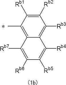
式(1b)中、Rb1~Rb7は、それぞれ独立に、水素原子または置換基を表す。*は結合位置を表す。また、Rb1~Rb7のうち隣り合う基同士は、連結して環を形成してもよい。
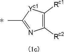
式(1c)中、Rc1およびRc2は、それぞれ独立に、水素原子または置換基を表す。Rc1とRc2とは互いに連結して環を形成してもよい。YC1は、硫黄原子、酸素原子、セレン原子、NRc3、または、CRc4Rc5を表す。Rc3~Rc5は、それぞれ独立に、水素原子または置換基を表す。*は結合位置を表す。
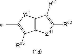
式(1d)中、Rd1~Rd3は、それぞれ独立に、水素原子または置換基を表す。Yd1は、硫黄原子、酸素原子、セレン原子、NRd4、または、CRd5Rd6を表す。Zd1は、硫黄原子、酸素原子、セレン原子、NRd7、CRd8Rd9、または、Rd10C=CRd11を表す。Rd4~Rd11は、それぞれ独立に、水素原子または置換基を表す。*は結合位置を表す。Rd1とRd2、Rd2とRd10またはRd2とRd11は、互いに連結して環を形成してもよい。

式(1e)中、Xe1は、窒素原子またはCRe2を表す。Ye1は、硫黄原子、酸素原子、セレン原子、NRe3、または、CRe4Re5を表す。Re1~Re6は、それぞれ独立に、水素原子または置換基を表す。Re1とRe2とは互いに連結して環を形成してもよい。*は結合位置を表す。

式(1i)中、Ri1およびRi2は、それぞれ独立に、水素原子または置換基を表す。Yi1は、硫黄原子、酸素原子、セレン原子、NRi3、または、CRi4Ri5を表す。Ri3~Ri5は、それぞれ独立に、水素原子または置換基を表す。*は結合位置を表す。 - 式(1)中、A1およびA2の両方が、前記式(1a)で表される置換基、前記式(1b)で表される置換基、前記式(1e)で表される置換基、および、前記式(1i)で表される置換基のいずれかを表す、請求項4に記載の光電変換素子。
- 式(1)中、A1およびA2の両方が、前記式(1a)で表される置換基、前記式(1b)で表される置換基、および、前記式(1i)で表される置換基のいずれかを表す、請求項4または5に記載の光電変換素子。
- 式(1)中、A1およびA2の両方が、同じ基を表す、請求項1~6のいずれか1項に記載の光電変換素子。
- 前記式(1)で表される化合物の分子量が、470~900である、請求項1~7のいずれか1項に記載の光電変換素子。
- 前記光電変換膜が、さらにn型有機半導体を含む、請求項1~8のいずれか1項に記載の光電変換素子。
- 前記光電変換膜が、さらにp型有機半導体を含む、請求項1~8のいずれか1項に記載の光電変換素子。
- さらに、電子ブロッキング膜を有する、請求項1~10のいずれか1項に記載の光電変換素子。
- さらに、正孔ブロッキング膜を有する、請求項1~11のいずれか1項に記載の光電変換素子。
- 請求項1~12のいずれか1項に記載の光電変換素子を含む光センサ。
- 請求項1~12のいずれか1項に記載の光電変換素子を含む撮像素子。
- 式(1)で表される化合物。
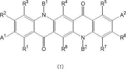
式(1)中、R1~R8は、それぞれ独立に、水素原子または置換基を表す。B1およびB2は、それぞれ独立に、水素原子または置換基を表す。A1およびA2は、それぞれ独立に、水素原子または置換基を表し、A1およびA2の少なくとも一方は、式(1a)~(1e)、および、式(1i)で表される置換基のいずれかを表す。また、R1~R8、A1、A2、B1およびB2のうち隣り合う基同士は、連結して環を形成してもよい。
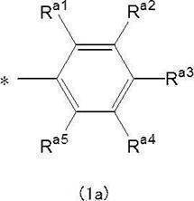
式(1a)中、Ra1~Ra5は、それぞれ独立に、水素原子、アルキル基、アリール基、ヘテロアリール基、アルコキシ基、アルキルチオ基、エチニル基、エテニル基、アシル基、ハロゲン原子、または、シリル基を表し、Ra1~Ra5のうち少なくとも1つはフッ素原子、塩素原子、臭素原子、フルオロアルキル基、および、シリル基のいずれかを表す。*は結合位置を表す。

式(1b)中、Rb1~Rb7は、それぞれ独立に、水素原子または置換基を表す。*は結合位置を表す。また、Rb1~Rb7のうち隣り合う基同士は、連結して環を形成してもよい。

式(1c)中、Rc1およびRc2は、それぞれ独立に、水素原子または置換基を表す。Rc1とRc2とは互いに連結して環を形成してもよい。YC1は、硫黄原子、酸素原子、セレン原子、NRc3、または、CRc4Rc5を表す。Rc3~Rc5は、それぞれ独立に、水素原子または置換基を表す。*は結合位置を表す。

式(1d)中、Rd1~Rd3は、それぞれ独立に、水素原子または置換基を表す。Yd1は、硫黄原子、酸素原子、セレン原子、NRd4、または、CRd5Rd6を表す。Zd1は、硫黄原子、酸素原子、セレン原子、NRd7、CRd8Rd9、または、Rd10C=CRd11を表す。Rd4~Rd11は、それぞれ独立に、水素原子または置換基を表す。*は結合位置を表す。Rd1とRd2、Rd2とRd10またはRd2とRd11は、互いに連結して環を形成してもよい。

式(1e)中、Xe1は、窒素原子またはCRe2を表す。Ye1は、硫黄原子、酸素原子、セレン原子、NRe3、または、CRe4Re5を表す。Re1~Re6は、それぞれ独立に、水素原子または置換基を表す。Re1とRe2とは互いに連結して環を形成してもよい。*は結合位置を表す。
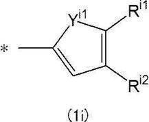
式(1i)中、Ri1およびRi2は、それぞれ独立に、水素原子、アルキル基、アリール基、または、ヘテロアリール基を表す。Yi1は、酸素原子、セレン原子、NRi3、または、CRi4Ri5を表す。Ri3~Ri5は、それぞれ独立に、水素原子または置換基を表す。*は結合位置を表す。
Priority Applications (3)
| Application Number | Priority Date | Filing Date | Title |
|---|---|---|---|
| JP2018529425A JP6675005B2 (ja) | 2016-07-27 | 2017-06-13 | 光電変換素子、撮像素子、光センサ、化合物 |
| KR1020197000282A KR102185032B1 (ko) | 2016-07-27 | 2017-06-13 | 광전 변환 소자, 촬상 소자, 광 센서, 화합물 |
| US16/238,528 US20190140189A1 (en) | 2016-07-27 | 2019-01-03 | Photoelectric conversion element, imaging element, optical sensor, and compound |
Applications Claiming Priority (4)
| Application Number | Priority Date | Filing Date | Title |
|---|---|---|---|
| JP2016-147177 | 2016-07-27 | ||
| JP2016147177 | 2016-07-27 | ||
| JP2016255209 | 2016-12-28 | ||
| JP2016-255209 | 2016-12-28 |
Related Child Applications (1)
| Application Number | Title | Priority Date | Filing Date |
|---|---|---|---|
| US16/238,528 Continuation US20190140189A1 (en) | 2016-07-27 | 2019-01-03 | Photoelectric conversion element, imaging element, optical sensor, and compound |
Publications (1)
| Publication Number | Publication Date |
|---|---|
| WO2018020871A1 true WO2018020871A1 (ja) | 2018-02-01 |
Family
ID=61016479
Family Applications (1)
| Application Number | Title | Priority Date | Filing Date |
|---|---|---|---|
| PCT/JP2017/021732 Ceased WO2018020871A1 (ja) | 2016-07-27 | 2017-06-13 | 光電変換素子、撮像素子、光センサ、化合物 |
Country Status (4)
| Country | Link |
|---|---|
| US (1) | US20190140189A1 (ja) |
| JP (1) | JP6675005B2 (ja) |
| KR (1) | KR102185032B1 (ja) |
| WO (1) | WO2018020871A1 (ja) |
Families Citing this family (4)
| Publication number | Priority date | Publication date | Assignee | Title |
|---|---|---|---|---|
| CN115516655A (zh) * | 2020-04-30 | 2022-12-23 | 富士胶片株式会社 | 光电转换元件、摄像元件、光传感器及化合物 |
| CN111944513B (zh) * | 2020-08-19 | 2023-06-09 | 浙江工业大学 | 一种基于喹吖啶酮的低驱动电压电致变色材料及其制备方法 |
| CN112094400B (zh) * | 2020-08-19 | 2023-06-09 | 浙江工业大学 | 一种基于喹吖啶酮-联二噻吩的橙红色-绿色显示电致变色材料及其制备方法 |
| CN112079831B (zh) * | 2020-08-26 | 2023-06-02 | 浙江工业大学 | 一种喹吖啶酮-噻吩衍生物及其制备方法与应用 |
Citations (4)
| Publication number | Priority date | Publication date | Assignee | Title |
|---|---|---|---|---|
| US5868828A (en) * | 1998-05-20 | 1999-02-09 | Bayer Corporation | Heterocyclic-substituted quinacridone pigments |
| JP2007059483A (ja) * | 2005-08-22 | 2007-03-08 | Fujifilm Corp | 光電変換素子、撮像素子、並びに、光電変換素子および撮像素子に電場を印加する方法 |
| JP2009280819A (ja) * | 2008-05-24 | 2009-12-03 | Lanxess Deutschland Gmbh | Lcd用カラーフィルターでのフッ素含有キナクリドン |
| KR20120105962A (ko) * | 2011-03-17 | 2012-09-26 | 서울대학교산학협력단 | 신규한 비대칭 퀴나크리돈 염료와 이를 이용한 염료감응 태양전지 |
Family Cites Families (7)
| Publication number | Priority date | Publication date | Assignee | Title |
|---|---|---|---|---|
| JPH02180884A (ja) * | 1988-12-29 | 1990-07-13 | Toyo Ink Mfg Co Ltd | 新規な化合物,およびそれを用いた顔料並びに電子写真感光体 |
| CN1219778C (zh) * | 2003-07-08 | 2005-09-21 | 吉林大学 | 喹吖啶酮衍生物及其在有机电致发光器件中的应用 |
| US8012530B2 (en) * | 2005-09-06 | 2011-09-06 | Kyoto University | Organic thin-film photoelectric conversion element and method of manufacturing the same |
| FR2899661B1 (fr) | 2006-04-06 | 2008-06-13 | Valeo Embrayages | Limiteur de couple |
| JP5683059B2 (ja) * | 2007-09-28 | 2015-03-11 | 富士フイルム株式会社 | 撮像素子 |
| CN102850348A (zh) * | 2012-10-08 | 2013-01-02 | 吉林大学 | 五苯基苯基喹吖啶酮衍生物及其在作为荧光材料方面应用 |
| KR102270705B1 (ko) * | 2013-12-06 | 2021-06-29 | 삼성전자주식회사 | 유기 광전 소자 및 이미지 센서 |
-
2017
- 2017-06-13 KR KR1020197000282A patent/KR102185032B1/ko active Active
- 2017-06-13 WO PCT/JP2017/021732 patent/WO2018020871A1/ja not_active Ceased
- 2017-06-13 JP JP2018529425A patent/JP6675005B2/ja active Active
-
2019
- 2019-01-03 US US16/238,528 patent/US20190140189A1/en not_active Abandoned
Patent Citations (4)
| Publication number | Priority date | Publication date | Assignee | Title |
|---|---|---|---|---|
| US5868828A (en) * | 1998-05-20 | 1999-02-09 | Bayer Corporation | Heterocyclic-substituted quinacridone pigments |
| JP2007059483A (ja) * | 2005-08-22 | 2007-03-08 | Fujifilm Corp | 光電変換素子、撮像素子、並びに、光電変換素子および撮像素子に電場を印加する方法 |
| JP2009280819A (ja) * | 2008-05-24 | 2009-12-03 | Lanxess Deutschland Gmbh | Lcd用カラーフィルターでのフッ素含有キナクリドン |
| KR20120105962A (ko) * | 2011-03-17 | 2012-09-26 | 서울대학교산학협력단 | 신규한 비대칭 퀴나크리돈 염료와 이를 이용한 염료감응 태양전지 |
Non-Patent Citations (1)
| Title |
|---|
| CHEN, JOHN JUN-AN ET AL.: "Quinacridone-Based Molecular Donors for Solution Processed Bulk- Heterojunction Organic Solar Cells", ACS APPLIED MATERIALS & INTERFACES, vol. 2, no. 9, 2010, pages 2679 - 2686, XP055456469 * |
Also Published As
| Publication number | Publication date |
|---|---|
| KR102185032B1 (ko) | 2020-12-01 |
| KR20190015515A (ko) | 2019-02-13 |
| JPWO2018020871A1 (ja) | 2019-05-09 |
| JP6675005B2 (ja) | 2020-04-01 |
| US20190140189A1 (en) | 2019-05-09 |
Similar Documents
| Publication | Publication Date | Title |
|---|---|---|
| JP7077326B2 (ja) | 光電変換素子、光センサ、撮像素子、化合物 | |
| US11785843B2 (en) | Photoelectric conversion element, optical sensor, and imaging element | |
| JP6047108B2 (ja) | 光電変換素子、撮像素子、光センサ | |
| WO2014156718A1 (ja) | 光電変換素子、撮像素子、光センサ、光電変換素子の使用方法 | |
| JPWO2019009249A1 (ja) | 光電変換素子、光センサ、撮像素子、および、化合物 | |
| JP6794530B2 (ja) | 光電変換素子、光センサ、撮像素子、および、化合物 | |
| US11024813B2 (en) | Photoelectric conversion element, optical sensor, and imaging element | |
| JP6535093B2 (ja) | 光電変換素子、撮像素子、光センサ、化合物 | |
| JP6675005B2 (ja) | 光電変換素子、撮像素子、光センサ、化合物 | |
| JP6674547B2 (ja) | 光電変換素子、撮像素子、光センサ、化合物 | |
| JP6684908B2 (ja) | 光電変換素子、撮像素子、光センサ、化合物 | |
| WO2014157009A1 (ja) | 光電変換素子、撮像素子、光センサ |
Legal Events
| Date | Code | Title | Description |
|---|---|---|---|
| 121 | Ep: the epo has been informed by wipo that ep was designated in this application |
Ref document number: 17833881 Country of ref document: EP Kind code of ref document: A1 |
|
| ENP | Entry into the national phase |
Ref document number: 20197000282 Country of ref document: KR Kind code of ref document: A |
|
| ENP | Entry into the national phase |
Ref document number: 2018529425 Country of ref document: JP Kind code of ref document: A |
|
| NENP | Non-entry into the national phase |
Ref country code: DE |
|
| 122 | Ep: pct application non-entry in european phase |
Ref document number: 17833881 Country of ref document: EP Kind code of ref document: A1 |