WO2018016554A1 - 障害内容特定装置、障害内容特定方法、及び、障害内容特定プログラムが格納された記録媒体 - Google Patents
障害内容特定装置、障害内容特定方法、及び、障害内容特定プログラムが格納された記録媒体 Download PDFInfo
- Publication number
- WO2018016554A1 WO2018016554A1 PCT/JP2017/026194 JP2017026194W WO2018016554A1 WO 2018016554 A1 WO2018016554 A1 WO 2018016554A1 JP 2017026194 W JP2017026194 W JP 2017026194W WO 2018016554 A1 WO2018016554 A1 WO 2018016554A1
- Authority
- WO
- WIPO (PCT)
- Prior art keywords
- power supply
- value
- failure
- power
- control process
- Prior art date
- Legal status (The legal status is an assumption and is not a legal conclusion. Google has not performed a legal analysis and makes no representation as to the accuracy of the status listed.)
- Ceased
Links
Images



Classifications
-
- G—PHYSICS
- G06—COMPUTING OR CALCULATING; COUNTING
- G06F—ELECTRIC DIGITAL DATA PROCESSING
- G06F11/00—Error detection; Error correction; Monitoring
- G06F11/30—Monitoring
- G06F11/3058—Monitoring arrangements for monitoring environmental properties or parameters of the computing system or of the computing system component, e.g. monitoring of power, currents, temperature, humidity, position, vibrations
-
- G—PHYSICS
- G06—COMPUTING OR CALCULATING; COUNTING
- G06F—ELECTRIC DIGITAL DATA PROCESSING
- G06F1/00—Details not covered by groups G06F3/00 - G06F13/00 and G06F21/00
- G06F1/26—Power supply means, e.g. regulation thereof
- G06F1/28—Supervision thereof, e.g. detecting power-supply failure by out of limits supervision
-
- G—PHYSICS
- G06—COMPUTING OR CALCULATING; COUNTING
- G06F—ELECTRIC DIGITAL DATA PROCESSING
- G06F1/00—Details not covered by groups G06F3/00 - G06F13/00 and G06F21/00
- G06F1/26—Power supply means, e.g. regulation thereof
- G06F1/30—Means for acting in the event of power-supply failure or interruption, e.g. power-supply fluctuations
-
- G—PHYSICS
- G06—COMPUTING OR CALCULATING; COUNTING
- G06F—ELECTRIC DIGITAL DATA PROCESSING
- G06F11/00—Error detection; Error correction; Monitoring
- G06F11/07—Responding to the occurrence of a fault, e.g. fault tolerance
- G06F11/0703—Error or fault processing not based on redundancy, i.e. by taking additional measures to deal with the error or fault not making use of redundancy in operation, in hardware, or in data representation
- G06F11/0751—Error or fault detection not based on redundancy
-
- G—PHYSICS
- G06—COMPUTING OR CALCULATING; COUNTING
- G06F—ELECTRIC DIGITAL DATA PROCESSING
- G06F11/00—Error detection; Error correction; Monitoring
- G06F11/07—Responding to the occurrence of a fault, e.g. fault tolerance
- G06F11/0703—Error or fault processing not based on redundancy, i.e. by taking additional measures to deal with the error or fault not making use of redundancy in operation, in hardware, or in data representation
- G06F11/0766—Error or fault reporting or storing
- G06F11/0769—Readable error formats, e.g. cross-platform generic formats, human understandable formats
-
- G—PHYSICS
- G06—COMPUTING OR CALCULATING; COUNTING
- G06F—ELECTRIC DIGITAL DATA PROCESSING
- G06F11/00—Error detection; Error correction; Monitoring
- G06F11/07—Responding to the occurrence of a fault, e.g. fault tolerance
- G06F11/0703—Error or fault processing not based on redundancy, i.e. by taking additional measures to deal with the error or fault not making use of redundancy in operation, in hardware, or in data representation
- G06F11/0766—Error or fault reporting or storing
- G06F11/0772—Means for error signaling, e.g. using interrupts, exception flags, dedicated error registers
-
- G—PHYSICS
- G06—COMPUTING OR CALCULATING; COUNTING
- G06F—ELECTRIC DIGITAL DATA PROCESSING
- G06F11/00—Error detection; Error correction; Monitoring
- G06F11/07—Responding to the occurrence of a fault, e.g. fault tolerance
- G06F11/0703—Error or fault processing not based on redundancy, i.e. by taking additional measures to deal with the error or fault not making use of redundancy in operation, in hardware, or in data representation
- G06F11/079—Root cause analysis, i.e. error or fault diagnosis
-
- G—PHYSICS
- G06—COMPUTING OR CALCULATING; COUNTING
- G06F—ELECTRIC DIGITAL DATA PROCESSING
- G06F11/00—Error detection; Error correction; Monitoring
- G06F11/30—Monitoring
- G06F11/32—Monitoring with visual or acoustical indication of the functioning of the machine
- G06F11/324—Display of status information
- G06F11/325—Display of status information by lamps or LED's
Definitions
- the present invention relates to a technique for identifying a failure content related to a power supply control system of a device.
- Patent Document 1 discloses a power supply control apparatus that detects a power supply sequence abnormality in a power supply unit in an apparatus that requires a plurality of power supplies having different control units. .
- This device controls a plurality of power supply devices that supply power, and power supply and power supply cutoff for these power supply devices. This device measures the time from when one of these power supply devices starts supplying power until another power supply device starts supplying power, and detects an abnormality in the power supply sequence according to the measurement result. To do.
- Patent Document 2 discloses a failure notification device for specifying a failure occurrence location before an initial diagnosis in an information processing device.
- the apparatus monitors a reset sequence by inputting a plurality of reset signals to a CPU (Central Processing Unit) and an IO (Input / Output) controller.
- This apparatus monitors a bus sequence by inputting a plurality of bus signals to a plurality of buses connected to a CPU.
- This device generates a first classification signal associated with the plurality of reset signals and a second classification signal associated with the plurality of bus signals.
- this apparatus notifies a failure location with a sound or a blinking signal by adding the said classification signal to the said several reset signal and bus signal, and outputting it.
- Patent Document 3 discloses a device that supplies power to a plurality of power domains with an optimal power sequence using a power sequence signal.
- Patent Document 4 discloses a failure diagnosis method that reduces the time required for failure simulation by reducing the storage capacity resources required for creating a failure dictionary and narrowing down target failures.
- the main object of the present invention is to provide a failure content identification device or the like that solves this problem.
- the failure content identification device is the main device or the power supply device in the process of turning on the power supply device that supplies power to the main device or the power supply control process for turning off the power supply device.
- a detection means for detecting that the value indicated by the power supply sequence signal whose value changes according to a predetermined specification has changed to a value indicating that the value is different from the predetermined specification, and the power supply by the detection means
- Generating means for generating information indicating the content of the power control process, which is performed at a timing when it is detected that the value indicated by the sequence signal has changed to a value indicating that the value is different from the predetermined specification; Prepare.
- a failure content specifying method is a power supply for turning on or off a power supply device that supplies power to a main device by an information processing device.
- the value indicated by the power sequence signal generated by the main device or the power supply device whose value changes according to a predetermined specification has changed to a value indicating that the value is different from the predetermined specification.
- the failure content specifying program includes a power supply control process for turning on the power supply device that supplies power to the main device or turning off the power supply device.
- a power supply control process for turning on the power supply device that supplies power to the main device or turning off the power supply device.
- the detection process and the detection process is performed at a timing at which it is detected that the value indicated by the power supply sequence signal has changed to a value indicating that it is different from the predetermined specification.
- the present invention can also be realized by a computer-readable non-volatile recording medium in which the failure content specifying program (computer program) is stored.
- the invention of the present application makes it possible to specify in a short time the content of a failure in the power supply control system related to the process of turning on or off the power supply of the apparatus.
- FIG. 1 It is a block diagram which shows the structure of the failure content specific
- FIG. 1 is a block diagram conceptually showing the structure of a failure content specifying apparatus 10 according to the first embodiment of the present invention.
- the failure content specifying device 10 transmits and receives power sequences (power) between the main device 20 and the power supply device 30.
- Sequence is an apparatus that identifies (determines and diagnoses) the contents of a failure that has occurred by observing a signal.
- the failure content identification device 10 may be an independent device or a device included in the main device 20 or the power supply device 30.
- Each power supply sequence signal described above is a value generated by the main device 20 or the power supply device 30 in the process of performing power supply control processing for turning the power supply device 30 on or off, for example, similarly to the configuration shown in Patent Document 3.
- the power supply sequence signal indicates, for example, that it has been detected that a switch for turning on or off the power supply device 30 has been operated by the user, or that a specific partial process included in the power supply control process has started or ended. It may be a signal indicating a state in which the control process proceeds.
- FIG. 2 is a time chart illustrating normal time transition of the value indicated by the power supply sequence signal when the power supply device 30 according to this embodiment is turned off.
- the operation of the failure content specifying device 10 when the power supply device 30 is turned off will be described. However, even when the power supply device 30 is turned on, the operation of the failure content specifying device 10 turns off the power supply device 30. It shall be the same as the case.
- P-SW at least “P-SW”, “PLT-RST”, “PS-ON”, “PWR-” are used as power sequence signals between the main device 20 and the power supply device 30. It is assumed that six signals “GD”, “PS-POWOK”, and “STBY” are transmitted and received. In the present embodiment, signals transmitted and received as the power supply sequence signal are not limited to these six signals.
- a signal “P-SW” is a signal indicating the on / off state of the power switch (power switch), and indicates that the operation to turn off the power to the power switch is performed by the user at time t1.
- a signal “STBY” is a signal indicating that the power supply device 30 is supplied with AC (Alternating Current) from the outside.
- a signal “PLT-RST”, a signal “PS-ON”, a signal “PWR-GD”, and a signal “PS-POWOK” are signals used in the power supply control process.
- the signal “PLT-RST”, the signal “PS-ON”, the signal “PWR-GD”, and the signal “PS-POWOK” each have a predetermined timing (for example, a timing at which a partial process starts or ends). The value changes from “1” to “0”.
- the values of “PWR-GD” and signal “PS-POWOK” change from “1” to “0” in order from time t1 to t5 (t1 ⁇ t2 ⁇ t3 ⁇ t4 ⁇ t5) according to the power supply specification. I decided to.
- the signal “STBY” is maintained at “1” unless the AC supply to the power supply device 30 is turned off.
- the failure content identification device 10 sequentially outputs signals whose values change from “1” to “0” at times tn and t (n + 1) (n is an integer of 1 to 4).
- n is an integer of 1 to 4.
- signal A and signal B it is possible to detect that a failure has occurred by detecting a state that violates the power supply specification such as “value indicated by signal A> value indicated by signal B”. .
- the failure content identification device 10 includes a detection unit 11, a generation unit 12, a display device 13, and a storage unit 14.
- the detection unit 11 and the generation unit 12 may be configured by a programmable logic circuit such as PLD (Programmable Logic) Device, or may be configured by a general logic circuit with fixed logic.
- PLD Programmable Logic
- the failure content identification device 10 starts operation when the power supply device 30 enters a power standby state in which AC is supplied from the outside, and resets the internal state to an initial state when the operation starts.
- PLD Programmable Logic
- the detection unit 11 includes comparison circuits 110 to 114 and FFs (flip flops) 115 to 119.
- the configurations and functions of the comparison circuits 110 to 114 are equivalent.
- the configurations and functions of the FFs 115 to 119 are equivalent.
- Clock signals (not shown in FIG. 1) are input to the FFs 115 to 119.
- FIG. 3 is a diagram illustrating a configuration of the comparison circuit 110 according to the present embodiment.
- the comparison circuit 110 includes NOT gates 1100 and 1101, AND gates 1102 to 1105, and an OR gate 1106, and these gates are connected as shown in FIG. However, “NOT” represents a logical negation, “AND” represents a logical product, and “OR” represents a logical sum.
- the comparison circuit 110 also includes an input X, an input Y, an output Q, an output L, and an output S as inputs and outputs.
- FIG. 4 is a diagram illustrating the relationship between the value input to the comparison circuit 110 illustrated in FIG. 3 and the value output from the comparison circuit 110.
- the values output from the output Q, the output L, and the output S are “1”, “0”, and “0” in this order.
- the signal “P-SW” and the signal “PLT_RST” illustrated in FIG. 2 are sequentially input to the input X and the input Y in the comparison circuit 110 according to the present embodiment.
- a signal “PLT_RST” and a signal “PS_ON” illustrated in FIG. 2 are sequentially input to the input X and the input Y in the comparison circuit 111.
- a signal “PS_ON” and a signal “PWR_GD” illustrated in FIG. 2 are sequentially input to the input X and the input Y in the comparison circuit 112.
- a signal “PWR_GD” and a signal “PS_POWOK” illustrated in FIG. 2 are sequentially input to the input X and the input Y in the comparison circuit 113.
- a signal “PS_POWOK” and a signal “STBY” illustrated in FIG. 2 are sequentially input to the input X and the input Y in the comparison circuit 114.
- the comparison circuit 110 inputs the output L illustrated in FIG. 3 to the FF 115 illustrated in FIG.
- the comparison circuit 111 inputs the output L to the FF 116.
- the comparison circuit 112 inputs the output L to the FF 117.
- the comparison circuit 113 inputs the output L to the FF 118.
- the comparison circuit 114 inputs the output L to the FF 119.
- the FF 115 inputs “0” to the generation unit 12 when the value indicated by the signal input from the comparison circuit 110 is “0”.
- the FF 115 changes the value input to the generation unit 12 from “0” to “1” when the value indicated by the signal input from the comparison circuit 110 changes from “0” to “1”.
- the state where “1” is input to the generation unit 12 is maintained.
- the FF 115 has a state that violates the power supply specification such that the value indicated by the signal “P-SW” is “1” and the value indicated by the signal “PLT_RST” is “0”.
- “1” is continuously input to the generation unit 12.
- Such an operation is possible, for example, by a configuration in which an output from an OR gate (not shown in FIG. 1) that inputs an output from the FF 115 and an output from the comparison circuit 110 is input to the FF 115.
- the FF 116 has a value that violates the power supply specification such that the value indicated by the signal “PLT_RST” is “1” and the value indicated by the signal “PS_ON” is “0”.
- “1” is continuously input to the generation unit 12.
- the FF 117 has a value “1” when the value indicated by the signal “PS_ON” is “1” and the value indicated by the signal “PWR_GD” is “0”. Is continuously input to the generation unit 12.
- the FF 118 is “1” when a value violating the power supply specification occurs such that the value indicated by the signal “PWR_GD” is “1” and the value indicated by the signal “PS_POWOK” is “0”. Is continuously input to the generation unit 12.
- the FF 119 displays “1” when a state that violates the power supply specification occurs such that the value indicated by the signal “PS_POWOK” is “1” and the value indicated by the signal “STBY” is “0”. Is continuously input to the generation unit 12.
- the generation unit 12 includes a decoding circuit 120.
- the decode circuit 120 generates a numerical value obtained by decoding the values input from the FFs 115 to 119. For example, when “1” is input from the FF 115, the decode circuit 120 generates “1” as a decoded numerical value. For example, when “1” is input from the FF 116, the decoding circuit 120 generates “2” as the decoded numerical value.
- the decoding circuit 120 when “1” is input from the FF 117, the decoding circuit 120 generates “3” as a decoded numerical value. For example, when “1” is input from the FF 118, the decode circuit 120 generates “4” as the decoded numerical value. For example, when “1” is input from the FF 119, the decode circuit 120 generates “5” as the decoded numerical value. For example, when the values input from the FFs 115 to 119 are all 0 (that is, a state that does not violate the power supply specification has occurred), the decoding circuit 120 generates “0” as the decoded numerical value.
- the decode circuit 120 displays the decoded numerical value on the display device 13, for example.
- the display device 13 is a device such as a liquid crystal monitor capable of displaying characters and numbers, for example.
- the generation unit 12 displays on the display device 13 information indicating the suspected member related to the failure that has been obtained by collating the decoded numerical value with the failure suspect dictionary information 140 stored in the storage unit 14. Also good.
- the storage unit 14 is a storage device such as an electronic memory or a magnetic disk.
- the failure suspect dictionary information 140 is information stored in the storage unit 14 by, for example, a user.
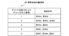
- FIG. 5 is a diagram illustrating a configuration of the suspected failure dictionary information 140 according to the present embodiment.
- the suspected failure dictionary information 140 is information that associates a numerical value decoded by the decoding circuit 120 with a suspected member relating to the occurred failure.
- the suspected dictionary information 140 illustrated in FIG. 5 for example, when the numerical value decoded by the decoding circuit 120 is “1”, that is, the values indicated by the signal “P-SW” and the signal “PLT_RST” are included in the power supply specification.
- the suspicious members are “member A” and “member B”.
- the failure suspected dictionary information 140 is information created by the user based on an analysis result for a failure that has occurred in the past, for example, as is generally done in creating a failure dictionary. For example, as a result of a user analyzing a failure that occurred in the past using an observation device, the timing at which the values of the signal “P-SW” and the signal “PLT_RST” change is opposite to the normal timing shown in FIG. (That is, corresponding to the case where the value decoded by the decoding circuit 120 is “1”). As a result of further analyzing the failure having such contents, there are a case where the failure of the member A is found and a case where the failure of the member B is found. In this case, as illustrated in FIG.
- the member A and the member B are registered in the failure suspicion dictionary information 140 as the suspicious members when the value decoded by the decoding circuit 120 is “1”. This is because, for example, the members involved in the generation of the signal “P-SW” and the signal “PLT_RST” are “member A” and “member B” included in the main device 20 or the power supply device 30. .
- a power supply control process for turning on or off the power supply device 30 is started by a user operation or the like (step S101).
- the comparison circuits 110 to 114 in the detection unit 11 compare the values indicated by the power supply sequence signal updated in each of the two consecutive partial processes (step S102).
- the FFs 115 to 119 in the detection unit 11 hold “1” input from the comparison circuits 110 to 114 and input to the decode circuit 120 (step). S104). If the comparison result conforms to the power supply specification (No in step S103), the FFs 115 to 119 hold “0” input from the comparison circuits 110 to 114 and input them to the decode circuit 120 (step S104). .
- step S106 If the power supply control process has not been completed (No in step S106), the process returns to step S102. When the power supply control process is completed (Yes in step S106), the process proceeds to step S107.
- the decoding circuit 120 in the generation unit 12 decodes the comparison result input from the FFs 115 to 119 (step S107).
- the generation unit 12 displays characters, numbers, and the like indicating that the power supply control process has been normally completed on the display device 13 (Step S109). This process ends.
- the generation unit 12 is information indicating the suspect member obtained by collating the decoding result with the failure suspect dictionary information 140 stored in the storage unit 14. Is displayed on the display device 13 (step S110), and the entire process ends.
- the failure content identification device 10 can identify the failure content of the power supply control system related to the process of turning on or off the device in a short time.
- the reason is that the detection unit 11 detects that the power supply sequence signal has changed to a value indicating that the power supply sequence signal is different from the power supply specification in the course of the power supply control process for turning on or off the power supply device 30, and the generation unit 12. This is because information indicating the content of the power control process performed at the timing when the power sequence signal has changed to a value indicating that it is different from the power specification is generated.
- the detection unit 11 turns on the power supply device 30 that supplies power to the main device 20 or turns off the power supply device 30.
- the value indicated by the power supply sequence signal generated by the main device 20 or the power supply device 30 whose value changes according to the predetermined power supply specification changes to a value indicating that the power supply specification is different from the power supply specification.
- the generation unit 12 indicates the content of the power supply control process performed at the timing when the detection unit 11 detects that the value indicated by the power supply sequence signal has changed to a value indicating that it is different from the power supply specification. Generate information.
- the failure content identification device 10 does not require the user to perform the above-described failure reproduction confirmation work, so that the failure content of the power supply control system related to the process of turning on or off the device can be reduced. Can be specified by time.
- the failure content identification device 10 further includes a storage unit 14 in which failure suspect dictionary information 140 is stored.
- the suspected failure dictionary information 140 is information that associates the content of the power supply control process with the suspected failure member in the main device 20 or the power supply device 30.
- the generation unit 12 uses the failure suspect dictionary information to indicate information indicating the content of the power control process performed at the timing when the value indicated by the power sequence signal is changed to a value indicating that the value is different from the power specification. By comparing with 140, information indicating the suspected failure member associated with the content of the power supply control process is obtained, and information indicating the suspected failure member is displayed on the display device 13, for example.
- the time required for searching for a suspected member using such suspected dictionary information is generally on the order of milliseconds or less.
- a user does not need to perform the reproduction confirmation work regarding the fault.
- the failure content specifying apparatus 10 can present information indicating the suspected failure member based on the generated failure content of the power supply control system to the user in a short time.
- the failure content identification device 10 avoids that the user performs the reproduction confirmation work again for the failure having the same content, the burden on the user can be reduced.
- the failure content identification device 10 may not include the storage unit 14.
- the decoding circuit 120 in the generation unit 12 displays the decoded numerical value on the display device 13 as it is.
- the display device 13 in this case may be a simple device such as a 7 segment LED (Light Emitting Diode) capable of displaying numerical values.
- the user performs power control processing performed at the timing when it is detected from the numerical value displayed on the display device 13 that the value indicated by the power supply sequence signal has changed to a value indicating that it is different from the power supply specification.
- the failure content identification device 10 according to the present embodiment can indicate to the user the result of identifying the failure content of the power supply control system related to the process of turning on or off the power supply of the device with a simple configuration.
- the detection unit 11 and the generation unit 12 according to the present embodiment are configured by a programmable logic circuit such as a PLD, for example.
- a programmable logic circuit such as a PLD
- the failure content identification device 10 according to the present embodiment can flexibly cope with the change when, for example, the generation specification of the power supply sequence signal is changed.
- the configurations of the detection unit 11 and the generation unit 12 according to the present embodiment are not limited to the configurations including the comparison circuits 110 to 114, the FFs 115 to 119, and the decoding circuit 120.
- the detection unit 11 and the generation unit 12 change in a complicated manner.
- a logic configuration capable of performing the above-described processing may be provided in accordance with the power supply sequence signal.
- a general technique can be adopted as a technique for designing such a logical configuration.
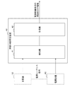
- FIG. 7 is a block diagram conceptually showing the structure of the fault content identification device 40 according to the second embodiment of the present invention.
- the failure content identification device 40 includes a detection unit 41 and a generation unit 42.
- the main device 50 or the power supply device 60 has a power supply whose value changes according to a predetermined specification.
- a sequence signal is generated.
- the detection unit 41 detects that the value indicated by the power supply sequence signal has changed to a value indicating that the value is different from the predetermined specification.
- the generation unit 42 detects the content of the power supply control process performed at the timing when the detection unit 41 detects that the value indicated by the power supply sequence signal has changed to a value indicating that the predetermined specification is different from the predetermined specification. Generate information to show.
- the failure content identification device 40 can identify the failure content of the power control system related to the process of turning on or off the power of the device in a short time.
- the reason is that the detection unit 41 detects that the power supply sequence signal has changed to a value indicating that it is different from the predetermined specification in the process of the power supply control process for turning on or off the power supply device 60, and the generation unit This is because information indicating the content of the power supply control process performed at the timing when the power supply sequence signal has changed to a value indicating that it differs from the predetermined specification is generated.
- each unit in the failure content specifying apparatus shown in FIGS. 1 and 7 can be realized by a dedicated HW (HardWare) (electronic circuit). 1 and 7, at least the following configuration can be regarded as a function (processing) unit (software module) of a software program.
- FIG. 8 is a diagram exemplarily illustrating the configuration of an information processing apparatus 900 (computer) that can execute the failure content identification apparatus according to each embodiment of the present invention. That is, FIG. 8 is a configuration of a computer (information processing apparatus) capable of realizing the failure content specifying apparatus shown in FIGS. 1 and 7, and a hardware environment capable of realizing each function in the above-described embodiment. Represents.
- the information processing apparatus 900 illustrated in FIG. 8 includes the following as constituent elements.
- CPU Central_Processing_Unit
- ROM Read_Only_Memory
- RAM Random_Access_Memory
- -Hard disk storage device
- a communication interface 905 with an external device ⁇ Bus 906 (communication line)
- the information processing apparatus 900 including the above-described components is a general computer in which these configurations are connected via a bus 906.
- the information processing apparatus 900 may include a plurality of CPUs 901 or may include a CPU 901 configured by a multi-core.
- the present invention described by taking the above embodiment as an example supplies a computer program capable of realizing the following functions to the information processing apparatus 900 shown in FIG.
- the function is the above-described configuration in the block configuration diagram (FIGS. 1 and 7) referred to in the description of the embodiment, or the function of the flowchart (FIG. 6).
- the present invention is then achieved by reading the computer program to the CPU 901 of the hardware, interpreting it and executing it.
- the computer program supplied to the apparatus may be stored in a readable / writable volatile memory (RAM 903) or a nonvolatile storage device such as the ROM 902 or the hard disk 904.
- RAM 903 readable / writable volatile memory
- nonvolatile storage device such as the ROM 902 or the hard disk 904.
- a general procedure can be adopted as a method for supplying a computer program into the hardware.
- the procedure includes, for example, a method of installing in the apparatus via various recording media 907 such as a CD-ROM, and a method of downloading from the outside via a communication line such as the Internet.
- the present invention is configured by a code constituting the computer program or a recording medium 907 in which the code is stored.
Landscapes
- Engineering & Computer Science (AREA)
- Theoretical Computer Science (AREA)
- Physics & Mathematics (AREA)
- General Engineering & Computer Science (AREA)
- General Physics & Mathematics (AREA)
- Quality & Reliability (AREA)
- Computing Systems (AREA)
- Health & Medical Sciences (AREA)
- Biomedical Technology (AREA)
- Power Sources (AREA)
Abstract
装置の電源をオンまたはオフする処理に関する電源制御系の障害内容を、短時間で特定する。 障害内容特定装置40は、主装置50に電源を供給する電源装置60をオンする、あるいは、電源装置60をオフする電源制御処理が進行する過程において、主装置50あるいは電源装置60によって生成される、値が所定の仕様に従って推移する電源シーケンス信号が示す値が、当該所定の仕様とは異なることを示す値に推移したことを検出する検出部41と、検出部41によって、電源シーケンス信号が示す値が、当該所定の仕様とは異なることを示す値に推移したことが検出されたタイミングに行われていた、電源制御処理の内容を示す情報を生成する生成部42と、を備える。
Description
本願発明は、装置の電源制御系に関する障害内容を特定する技術に関する。
情報化が高度に発達した現代社会においては、情報処理システムにおいて発生した障害が社会に与える影響は非常に大きい。したがって、情報処理システムにおいて発生した障害を適切に検出し、障害内容を特定する技術に対する期待が高まってきている。
このような技術に関連する技術として、特許文献1には、制御単位が異なる複数の電源を必要とする装置において、被電源供給部において電源シーケンスの異常を検出する電源制御装置が開示されている。この装置は、電源を供給する複数の電源装置と、それらの電源装置に対して、電源の供給及び電源の遮断を制御する。そしてこの装置は、それらの電源装置のいずれかが電源供給を開始してから、他の電源装置が電源供給を開始するまでの時間を計測し、その計測結果に応じて電源シーケンスの異常を検出する。
また、特許文献2には、情報処理装置において、初期診断以前の障害発生箇所を特定する障害通知装置が開示されている。その装置は、CPU(Central Processing Unit)とIO(Input/Output)コントローラに、複数のリセット信号を入力することにより、リセットシーケンスを監視する。この装置は、CPUに接続されている複数のバスに、複数のバス信号を入力することにより、バスシーケンスを監視する。この装置は、当該複数のリセット信号に紐付けされる第1の分別信号、及び、当該複数のバス信号に紐付けされる第2の分別信号を生成する。そしてこの装置は、当該複数のリセット信号とバス信号に、当該分別信号を付加して出力することにより、音や点滅信号によって障害箇所を通知する。
また、特許文献3には、電源シーケンス信号を用いて、最適な電源シーケンスで複数の電源ドメインに電源を供給する装置が開示されている。
また、特許文献4には、故障辞書の作成に要する記憶容量資源を削減し、対象故障を絞り込むことによって、故障シミュレーションに要する時間を短縮する故障診断方式が開示されている。
情報処理装置の電源をオンあるいはオフする際にハードウェア障害が発生した場合、ハードウェアあるいはソフトウェアが、障害の原因を示すログを生成できないことが多い。このような場合、障害の原因を特定するために、例えば、電源シーケンス信号等を観測できるように、プリント基板等に対して物理的な布線を行ったのち、ロジックアナライザ等の観測機器を用いて電源シーケンス信号等を観測することによって、障害内容を解析することが一般的に行われている。この場合、障害における被疑部材を交換したのち障害の再現確認を行うことを繰り返して行うことが必要となる他、障害の再現は、情報処理システムの環境あるいは構成等に依存することも多いので、障害部材の特定に多大な時間がかかるという問題がある。特許文献1乃至4において開示された構成は、この問題を解決するのに十分であるとは言えない。本願発明の主たる目的は、この課題を解決する障害内容特定装置等を提供することである。
本願発明の一態様に係る障害内容特定装置は、主装置に電源を供給する電源装置をオンする、あるいは、前記電源装置をオフする電源制御処理が進行する過程において、前記主装置あるいは前記電源装置によって生成される、値が所定の仕様に従って推移する電源シーケンス信号が示す値が、前記所定の仕様とは異なることを示す値に推移したことを検出する検出手段と、前記検出手段によって、前記電源シーケンス信号が示す値が、前記所定の仕様とは異なることを示す値に推移したことが検出されたタイミングに行われていた、前記電源制御処理の内容を示す情報を生成する生成手段と、を備える。
上記目的を達成する他の見地において、本願発明の一態様に係る障害内容特定方法は、情報処理装置によって、主装置に電源を供給する電源装置をオンする、あるいは、前記電源装置をオフする電源制御処理が進行する過程において、前記主装置あるいは前記電源装置によって生成される、値が所定の仕様に従って推移する電源シーケンス信号が示す値が、前記所定の仕様とは異なることを示す値に推移したことを検出し、検出した前記電源シーケンス信号が示す値が、前記所定の仕様とは異なることを示す値に推移したことが検出されたタイミングに行われていた、前記電源制御処理の内容を示す情報を生成する。
また、上記目的を達成する更なる見地において、本願発明の一態様に係る障害内容特定プログラムは、主装置に電源を供給する電源装置をオンする、あるいは、前記電源装置をオフする電源制御処理が進行する過程において、前記主装置あるいは前記電源装置によって生成される、値が所定の仕様に従って推移する電源シーケンス信号が示す値が、前記所定の仕様とは異なることを示す値に推移したことを検出する検出処理と、前記検出処理によって、前記電源シーケンス信号が示す値が、前記所定の仕様とは異なることを示す値に推移したことが検出されたタイミングに行われていた、前記電源制御処理の内容を示す情報を生成する生成処理と、をコンピュータに実行させるためのプログラムである。
更に、本願発明は、係る障害内容特定プログラム(コンピュータプログラム)が格納された、コンピュータ読み取り可能な、不揮発性の記録媒体によっても実現可能である。
本願発明は、装置の電源をオンまたはオフする処理に関する電源制御系の障害内容を、短時間で特定することを可能とする。
以下、本願発明の実施の形態について図面を参照して詳細に説明する。
<第1の実施形態>
図1は、本願発明の第1の実施の形態に係る障害内容特定装置10の構成を概念的に示すブロック図である。障害内容特定装置10は、例えば情報処理装置である主装置20に電源を供給する電源装置30をオンあるいはオフする際に、主装置20と電源装置30との間で送受信される電源シーケンス(パワーシーケンス)信号を観測することによって、発生した障害内容を特定(判定、診断)する装置である。障害内容特定装置10は、独立した装置であってもよいし、主装置20あるいは電源装置30に含まれる装置であってもよい。
図1は、本願発明の第1の実施の形態に係る障害内容特定装置10の構成を概念的に示すブロック図である。障害内容特定装置10は、例えば情報処理装置である主装置20に電源を供給する電源装置30をオンあるいはオフする際に、主装置20と電源装置30との間で送受信される電源シーケンス(パワーシーケンス)信号を観測することによって、発生した障害内容を特定(判定、診断)する装置である。障害内容特定装置10は、独立した装置であってもよいし、主装置20あるいは電源装置30に含まれる装置であってもよい。
上述した各電源シーケンス信号は、例えば、特許文献3に示す構成と同様に、電源装置30をオンあるいはオフする電源制御処理が進行する過程において、主装置20あるいは電源装置30によって生成される、値が所定のタイミングで変化する(値が所定の仕様に従って推移する)信号である。電源シーケンス信号は、例えば、電源装置30をオンあるいはオフするスイッチがユーザによって操作されたことを検出したこと、あるいは、電源制御処理に含まれる特定の部分処理が、開始あるいは終了したことなど、電源制御処理が進行する状態を示す信号であってもよい。
図2は、本実施形態に係る電源装置30をオフする場合において、電源シーケンス信号が示す値の正常な時間推移を例示するタイムチャートである。本願では以降、電源装置30をオフする場合における障害内容特定装置10の動作を説明するが、電源装置30をオンする場合にいても、障害内容特定装置10の動作は、電源装置30をオフする場合と同様であることとする。
本実施形態では、図2に示す通り、主装置20と電源装置30との間において、電源シーケンス信号として、少なくとも「P-SW」、「PLT-RST」、「PS-ON」、「PWR-GD」、「PS-POWOK」、「STBY」という6つの信号が送受信されることとする。尚、本実施形態において、電源シーケンス信号として送受信される信号は、これら6つの信号に限定されない。
図2において、信号「P-SW」は、電源スイッチ(パワースイッチ)のオン/オフ状態を示す信号であり、時間t1において、電源スイッチに対する電源をオフする操作が、ユーザによって行われたことを示している。図2において、信号「STBY」は、電源装置30が外部からAC(Alternating Current)供給されていることを示す信号である。図2において、信号「PLT-RST」、信号「PS-ON」、信号「PWR-GD」、及び、信号「PS-POWOK」は、電源制御処理において使用される信号である。信号「PLT-RST」、信号「PS-ON」、信号「PWR-GD」、及び、信号「PS-POWOK」は、それぞれ、所定のタイミング(例えば、ある部分処理が開始あるいは終了したタイミング)に、値が「1」から「0」に推移する。
図2に示す通り、本実施形態に係る電源装置30をオフする電源制御処理が正常に行われた場合、信号「P-SW」、信号「PLT-RST」、信号「PS-ON」、信号「PWR-GD」、及び、信号「PS-POWOK」は、電源仕様に従って、順に、時間t1乃至t5(t1<t2<t3<t4<t5)において、値が「1」から「0」に推移することとする。信号「STBY」は、電源装置30に対するAC供給がオフされない限り、「1」を維持することとする。したがって、本実施形態に係る障害内容特定装置10は、時間tn、t(n+1)(nは1乃至4のいずれかの整数)に値が「1」から「0」に推移する信号を、順に、信号A及び信号Bとした場合、「信号Aが示す値>信号Bが示す値」というような、電源仕様に違反する状態を検出することによって、障害が発生したことを検出することができる。
図1に示す通り、本実施形態に係る障害内容特定装置10は、検出部11、生成部12、表示装置13、及び、記憶部14を備えている。検出部11及び生成部12は、例えば、PLD(Programmable Logic Device)等のプログラム可能な論理回路によって構成されてもよいし、論理が固定された一般的な論理回路によって構成されてもよい。障害内容特定装置10は、例えば、電源装置30が外部からAC供給されている電源スタンバイ状態になったときに動作を開始し、動作を開始するときに、内部の状態を初期状態にリセットすることとする。
検出部11は、比較回路110乃至114、及び、FF(フリップフロップ)115乃至119を内包している。比較回路110乃至114の構成及び機能は同等である。FF115乃至119の構成及び機能は同等である。FF115乃至119にはクロック信号(図1には不図示)が入力されている。
図3は、本実施形態に係る比較回路110の構成を例示する図である。比較回路110は、NOTゲート1100及び1101、ANDゲート1102乃至1105、及び、ORゲート1106を含み、それらのゲートが図3に示す通りに接続された回路である。但し、「NOT」は論理否定、「AND」は論理積、「OR」は論理和を表す。比較回路110は、また、入出力として、入力X、入力Y、出力Q、出力L、及び、出力Sを備えている。
図4は、図3が例示する比較回路110へ入力される値と、比較回路110から出力される値との関係を例示する図である。図4に例示する通り、比較回路110における入力X及び入力Yに対して、「X=Y」を満たす値(すなわち、X及びYが共に「0」あるいは共に「1」である)が入力された場合は、出力Q、出力L、及び、出力Sから出力される値は、順に、「1」、「0」、及び、「0」となる。比較回路110における入力X及び入力Yに対して、「X>Y」を満たす値(すなわち、Xが「1」であり、Yが「0」である)が入力された場合は、出力Q、出力L、及び、出力Sから出力される値は、順に、「0」、「1」、及び、「0」となる。比較回路110における入力X及び入力Yに対して、「X<Y」を満たす値(すなわち、Xが「0」であり、Yが「1」である)が入力された場合は、出力Q、出力L、及び、出力Sから出力される値は、順に、「0」、「0」、及び、「1」となる。
本実施形態に係る比較回路110における入力X及び入力Yには、順に、図2に例示する信号「P-SW」及び信号「PLT_RST」が入力される。比較回路111における入力X及び入力Yには、順に、図2に例示する信号「PLT_RST」及び信号「PS_ON」が入力される。比較回路112における入力X及び入力Yには、順に、図2に例示する信号「PS_ON」及び信号「PWR_GD」が入力される。比較回路113における入力X及び入力Yには、順に、図2に例示する信号「PWR_GD」及び信号「PS_POWOK」が入力される。比較回路114における入力X及び入力Yには、順に、図2に例示する信号「PS_POWOK」及び信号「STBY」が入力される。
比較回路110は、図3に例示する出力Lを、図1に例示するFF115に入力する。比較回路111は、出力Lを、FF116に入力する。比較回路112は、出力Lを、FF117に入力する。比較回路113は、出力Lを、FF118に入力する。比較回路114は、出力Lを、FF119に入力する。
本実施形態に係るFF115は、比較回路110から入力された信号が示す値が、「0」である場合は、「0」を生成部12へ入力する。FF115は、比較回路110から入力された信号が示す値が、「0」から「1」に推移したときに、生成部12へ入力する値を「0」から「1」へ変更し、その後も、生成部12へ「1」を入力する状態を維持する。すなわち、FF115は、信号「P-SW」が示す値が「1」であり、かつ、信号「PLT_RST」が示す値が「0」であるというような、電源仕様に違反する状態が発生した場合に、「1」を継続して生成部12へ入力する。このような動作は、例えば、FF115からの出力と比較回路110からの出力とを入力するORゲート(図1には不図示)からの出力をFF115に入力する構成により可能である。
同様に、FF116は、信号「PLT_RST」が示す値が「1」であり、かつ、信号「PS_ON」が示す値が「0」であるというような、電源仕様に違反する状態が発生した場合に、「1」を継続して生成部12へ入力する。FF117は、信号「PS_ON」が示す値が「1」であり、かつ、信号「PWR_GD」が示す値が「0」であるというような、電源仕様に違反する状態が発生した場合に、「1」を継続して生成部12へ入力する。FF118は、信号「PWR_GD」が示す値が「1」であり、かつ、信号「PS_POWOK」が示す値が「0」であるというような、電源仕様に違反する状態が発生した場合に、「1」を継続して生成部12へ入力する。FF119は、信号「PS_POWOK」が示す値が「1」であり、かつ、信号「STBY」が示す値が「0」であるというような、電源仕様に違反する状態が発生した場合に、「1」を継続して生成部12へ入力する。 図1に示す通り、本実施形態に係る生成部12は、デコード回路120を内包している。デコード回路120は、FF115乃至119から入力された値をデコードした数値を生成する。デコード回路120は、例えば、FF115から「1」を入力された場合に、デコードした数値として「1」を生成する。デコード回路120は、例えば、FF116から「1」を入力された場合に、デコードした数値として「2」を生成する。デコード回路120は、例えば、FF117から「1」を入力された場合に、デコードした数値として「3」を生成する。デコード回路120は、例えば、FF118から「1」を入力された場合に、デコードした数値として「4」を生成する。デコード回路120は、例えば、FF119から「1」を入力された場合に、デコードした数値として「5」を生成する。デコード回路120は、例えば、FF115乃至119から入力された値が全て0である(すなわち、電源仕様に違反する状態が発生していない)場合に、デコードした数値として「0」を生成する。
デコード回路120は、デコードした数値を、例えば、表示装置13に表示する。表示装置13は、例えば、文字や数字を表示可能な液晶モニタ等の装置である。
生成部12は、当該デコードした数値を、記憶部14に記憶された障害被疑辞書情報140と照合することによって得られた、発生した障害に関する被疑部材を示す情報を、表示装置13に表示してもよい。記憶部14は、電子メモリあるいは磁気ディスク等の記憶デバイスである。障害被疑辞書情報140は、例えばユーザによって、記憶部14に記憶された情報である。
図5は、本実施形態に係る障害被疑辞書情報140の構成を例示する図である。図5に例示する通り、障害被疑辞書情報140は、デコード回路120によりデコードされた数値と、発生した障害に関する被疑部材とを関連付ける情報である。図5に例示する障害被疑辞書情報140は、例えば、デコード回路120によりデコードされた数値が「1」である場合、すなわち、信号「P-SW」及び信号「PLT_RST」が示す値が電源仕様に違反する値になった場合において、被疑部材は、「部材A」及び「部材B」であることを示している。
障害被疑辞書情報140は、例えば、障害辞書の作成において一般的に行われているように、過去に発生した障害に対する解析結果に基づいて、ユーザによって作成された情報である。例えば、過去に発生した障害をユーザが観測機器を用いて解析した結果、信号「P-SW」と信号「PLT_RST」について、値が変化するタイミングが図2に示す正常なタイミングとは逆転していた(即ち、デコード回路120によりデコードされた値が「1」となるケースに相当)とする。そしてこのような内容の障害をさらに解析した結果として、部材Aの故障が判明した場合と、部材Bの故障が判明した場合とが存在することとする。この場合、図5に例示する通り、デコード回路120によりデコードされた値が「1」となる場合における被疑部材として、部材A及び部材Bが、障害被疑辞書情報140に登録される。このことは、例えば、信号「P-SW」及び信号「PLT_RST」の生成に関与する部材は、主装置20あるいは電源装置30に含まれる「部材A」及び「部材B」であることに起因する。
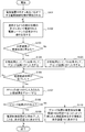
次に図6のフローチャートを参照して、本実施形態に係る障害内容特定装置10の動作(処理)について詳細に説明する。
ユーザによる操作等により、電源装置30をオンあるいはオフする電源制御処理が開始される(ステップS101)。検出部11における比較回路110乃至114は、連続する2つの部分処理の個々において更新される電源シーケンス信号が示す値を比較する(ステップS102)。
その比較結果が電源仕様と異なる場合(ステップS103でYes)、検出部11におけるFF115乃至119は、比較回路110乃至114から入力された「1」を保持して、デコード回路120へ入力する(ステップS104)。その比較結果が電源仕様の通りである場合(ステップS103でNo)、FF115乃至119は、比較回路110乃至114から入力された「0」を保持して、デコード回路120へ入力する(ステップS104)。
電源制御処理が完了していない場合(ステップS106でNo)、処理はステップS102へ戻る。電源制御処理が完了した場合(ステップS106でYes)、処理はステップS107へ進む。
生成部12におけるデコード回路120は、FF115乃至119から入力された比較結果をデコードする(ステップS107)。そのデコード結果が「0」である場合(ステップS108でYes)、生成部12は、電源制御処理が正常終了したことを表す文字や数字等を、表示装置13に表示し(ステップS109)、全体の処理は終了する。そのデコード結果が「0」でない場合(ステップS108でNo)、生成部12は、デコード結果を、記憶部14に記憶された障害被疑辞書情報140と照合することによって得られた被疑部材を示す情報を、表示装置13に表示し(ステップS110)、全体の処理は終了する。
本実施形態に係る障害内容特定装置10は、装置の電源をオンまたはオフする処理に関する電源制御系の障害内容を、短時間で特定することができる。その理由は、検出部11は、電源装置30をオンまたはオフする電源制御処理が進行する過程において、電源シーケンス信号が電源仕様とは異なることを示す値に推移したことを検出し、生成部12は、電源シーケンス信号が電源仕様とは異なることを示す値に推移したタイミングに行われていた電源制御処理の内容を示す情報を生成するからである。
以下に、本実施形態に係る障害内容特定装置10によって実現される効果について、詳細に説明する。
情報処理装置の電源をオンあるいはオフする際にハードウェア障害が発生した場合、ハードウェアあるいはソフトウェアが、障害の原因を示すログを生成できないことが多い。このような場合、障害の原因を特定するために、例えば、電源シーケンス信号等を観測できるように、プリント基板等に対する物理的な布線を行ったのち、ロジックアナライザ等の観測機器を用いて電源シーケンス信号等を観測することによって、障害内容を解析することが一般的に行われている。この場合、障害における被疑部材を交換したのち障害の再現確認を行うことを繰り返して行うことが必要となる他、障害の再現は、情報処理システムの環境あるいは構成等に依存することも多いので、障害部材の特定に多大な時間がかかるという問題がある。
このような問題を解決するために、本実施形態に係る障害内容特定装置10では、検出部11は、主装置20に電源を供給する電源装置30をオンする、あるいは、電源装置30をオフする電源制御処理が進行する過程において、主装置20あるいは電源装置30によって生成される、値が所定の電源仕様に従って推移する電源シーケンス信号が示す値が、その電源仕様とは異なることを示す値に推移したことを検出する。そして生成部12は、検出部11によって、電源シーケンス信号が示す値が、電源仕様とは異なることを示す値に推移したことが検出されたタイミングに行われていた、電源制御処理の内容を示す情報を生成する。これにより、本実施形態に係る障害内容特定装置10は、上述した障害の再現確認作業をユーザが行なわずに済むので、装置の電源をオンまたはオフする処理に関する電源制御系の障害内容を、短時間で特定することができる。
また、本実施形態に係る障害内容特定装置10は、障害被疑辞書情報140が記憶された記憶部14をさらに備えている。障害被疑辞書情報140は、電源制御処理の内容と、主装置20あるいは電源装置30における障害被疑部材と、を関連付ける情報である。生成部12は、電源シーケンス信号が示す値が、電源仕様とは異なることを示す値に推移したことが検出されたタイミングに行われていた電源制御処理の内容を示す情報を、障害被疑辞書情報140と照合することによって、その電源制御処理の内容に関連付けられた障害被疑部材を示す情報を入手し、入手した障害被疑部材を示す情報を、例えば、表示装置13に表示する。現在の検索技術では、比較的大規模なシステム構成においても、このような障害被疑辞書情報を用いた障害被疑部材の検索に要する時間は、一般的に例えばミリセカンド以下のオーダである。そして、障害被疑辞書情報に登録済みである障害に関しては、ユーザは当該障害に関する再現確認作業を行なう必要がなくなる。これにより、本実施形態に係る障害内容特定装置10は、発生した電源制御系の障害内容に基づく障害被疑部材を示す情報を短時間にユーザに提示することができる。そして、障害内容特定装置10は、ユーザが同じ内容の障害に対して再現確認作業を再度行なうことを回避するので、ユーザの負担を軽減することができる。
また、本実施形態に係る障害内容特定装置10は、記憶部14を備えなくてもよい。この場合、生成部12におけるデコード回路120は、デコードした数値を、そのまま表示装置13に表示する。この場合の表示装置13は、例えば、数値を表示可能な7セグメントLED(Light Emitting Diode)等の簡易な装置であればよい。この場合、ユーザは、表示装置13に表示された数値から、電源シーケンス信号が示す値が、電源仕様とは異なることを示す値に推移したことが検出されたタイミングに行われていた電源制御処理の内容を把握することができる。したがって、この場合、本実施形態に係る障害内容特定装置10は、装置の電源をオンまたはオフする処理に関する電源制御系の障害内容を特定した結果を、簡易な構成によりユーザに示すことができる。
また、本実施形態に係る検出部11及び生成部12は、例えば、PLD等のプログラム可能な論理回路によって構成されている。これにより、本実施形態に係る障害内容特定装置10は、例えば、電源シーケンス信号の生成仕様が変更された場合に、その変更に柔軟に対応することができる。
尚、本実施形態に係る検出部11及び生成部12の構成は、比較回路110乃至114、FF115乃至119、及び、デコード回路120を備えた構成に限定されない。例えば、主装置20あるいは電源装置30によって生成される電源シーケンス信号が、図2に例示するタイムチャートと比較して複雑に値が推移する場合、検出部11及び生成部12は、複雑に推移する電源シーケンス信号に合わせて、上述した処理を行うことが可能な論理構成を備えればよい。このような論理構成を設計する技術自体には、現在では一般的な技術を採用することができる。
<第2の実施形態>
図7は、本願発明の第2の実施形態に係る障害内容特定装置40の構成を概念的に示すブロック図である。障害内容特定装置40は、検出部41、及び、生成部42を備えている。
図7は、本願発明の第2の実施形態に係る障害内容特定装置40の構成を概念的に示すブロック図である。障害内容特定装置40は、検出部41、及び、生成部42を備えている。
主装置50に電源を供給する電源装置60をオンする、あるいは、電源装置60をオフする電源制御処理が進行する過程において、主装置50あるいは電源装置60は、値が所定の仕様に従って推移する電源シーケンス信号を生成する。検出部41は、その電源シーケンス信号が示す値が、当該所定の仕様とは異なることを示す値に推移したことを検出する。
生成部42は、検出部41によって、電源シーケンス信号が示す値が、当該所定の仕様とは異なることを示す値に推移したことが検出されたタイミングに行われていた、電源制御処理の内容を示す情報を生成する。
本実施形態に係る障害内容特定装置40は、装置の電源をオンまたはオフする処理に関する電源制御系の障害内容を、短時間で特定することができる。その理由は、検出部41は、電源装置60をオンまたはオフする電源制御処理が進行する過程において、電源シーケンス信号が所定の仕様とは異なることを示す値に推移したことを検出し、生成部42は、電源シーケンス信号が所定の仕様とは異なることを示す値に推移したタイミングに行われていた電源制御処理の内容を示す情報を生成するからである。
<ハードウェア構成例>
上述した各実施形態において図1、及び、図7に示した障害内容特定装置における各部は、専用のHW(HardWare)(電子回路)によって実現することができる。また、図1、及び、図7において、少なくとも、下記構成は、ソフトウェアプログラムの機能(処理)単位(ソフトウェアモジュール)と捉えることができる。
・検出部11及び41、
・生成部12及び42。
上述した各実施形態において図1、及び、図7に示した障害内容特定装置における各部は、専用のHW(HardWare)(電子回路)によって実現することができる。また、図1、及び、図7において、少なくとも、下記構成は、ソフトウェアプログラムの機能(処理)単位(ソフトウェアモジュール)と捉えることができる。
・検出部11及び41、
・生成部12及び42。
但し、これらの図面に示した各部の区分けは、説明の便宜上の構成であり、実装に際しては、様々な構成が想定され得る。この場合のハードウェア環境の一例を、図8を参照して説明する。
図8は、本願発明の各実施形態に係る障害内容特定装置を実行可能な情報処理装置900(コンピュータ)の構成を例示的に説明する図である。即ち、図8は、図1、及び、図7に示した障害内容特定装置を実現可能なコンピュータ(情報処理装置)の構成であって、上述した実施形態における各機能を実現可能なハードウェア環境を表す。
図8に示した情報処理装置900は、構成要素として下記を備えている。
・CPU(Central_Processing_Unit)901、
・ROM(Read_Only_Memory)902、
・RAM(Random_Access_Memory)903、
・ハードディスク(記憶装置)904、
・外部装置との通信インタフェース905、
・バス906(通信線)、
・CD-ROM(Compact_Disc_Read_Only_Memory)等の記録媒体907に格納されたデータを読み書き可能なリーダライタ908、
・入出力インタフェース909。
・CPU(Central_Processing_Unit)901、
・ROM(Read_Only_Memory)902、
・RAM(Random_Access_Memory)903、
・ハードディスク(記憶装置)904、
・外部装置との通信インタフェース905、
・バス906(通信線)、
・CD-ROM(Compact_Disc_Read_Only_Memory)等の記録媒体907に格納されたデータを読み書き可能なリーダライタ908、
・入出力インタフェース909。
即ち、上記構成要素を備える情報処理装置900は、これらの構成がバス906を介して接続された一般的なコンピュータである。情報処理装置900は、CPU901を複数備える場合もあれば、マルチコアにより構成されたCPU901を備える場合もある。
そして、上述した実施形態を例に説明した本願発明は、図8に示した情報処理装置900に対して、次の機能を実現可能なコンピュータプログラムを供給する。その機能とは、その実施形態の説明において参照したブロック構成図(図1、及び、図7)における上述した構成、或いはフローチャート(図6)の機能である。本願発明は、その後、そのコンピュータプログラムを、当該ハードウェアのCPU901に読み出して解釈し実行することによって達成される。また、当該装置内に供給されたコンピュータプログラムは、読み書き可能な揮発性のメモリ(RAM903)、または、ROM902やハードディスク904等の不揮発性の記憶デバイスに格納すれば良い。
また、前記の場合において、当該ハードウェア内へのコンピュータプログラムの供給方法は、現在では一般的な手順を採用することができる。その手順としては、例えば、CD-ROM等の各種記録媒体907を介して当該装置内にインストールする方法や、インターネット等の通信回線を介して外部よりダウンロードする方法等がある。そして、このような場合において、本願発明は、係るコンピュータプログラムを構成するコード或いは、そのコードが格納された記録媒体907によって構成されると捉えることができる。
以上、上述した実施形態を模範的な例として本願発明を説明した。しかしながら、本願発明は、上述した実施形態には限定されない。即ち、本願発明は、本願発明のスコープ内において、当業者が理解し得る様々な態様を適用することができる。
この出願は、2016年7月21日に出願された日本出願特願2016-143478を基礎とする優先権を主張し、その開示の全てをここに取り込む。
10 障害内容特定装置
11 検出部
110乃至114 比較回路
1100及び1101 NOTゲート
1102乃至1105 ANDゲート
1106 ORゲート
115乃至119 FF
12 生成部
120 デコード回路
13 表示装置
14 記憶部
140 障害被疑辞書情報
20 主装置
30 電源装置
40 障害内容特定装置
41 検出部
42 生成部
50 主装置
60 電源装置
900 情報処理装置
901 CPU
902 ROM
903 RAM
904 ハードディスク(記憶装置)
905 通信インタフェース
906 バス
907 記録媒体
908 リーダライタ
909 入出力インタフェース
11 検出部
110乃至114 比較回路
1100及び1101 NOTゲート
1102乃至1105 ANDゲート
1106 ORゲート
115乃至119 FF
12 生成部
120 デコード回路
13 表示装置
14 記憶部
140 障害被疑辞書情報
20 主装置
30 電源装置
40 障害内容特定装置
41 検出部
42 生成部
50 主装置
60 電源装置
900 情報処理装置
901 CPU
902 ROM
903 RAM
904 ハードディスク(記憶装置)
905 通信インタフェース
906 バス
907 記録媒体
908 リーダライタ
909 入出力インタフェース
Claims (10)
- 主装置に電源を供給する電源装置をオンする、あるいは、前記電源装置をオフする電源制御処理が進行する過程において、前記主装置あるいは前記電源装置によって生成される、値が所定の仕様に従って推移する電源シーケンス信号が示す値が、前記所定の仕様とは異なることを示す値に推移したことを検出する検出手段と、
前記検出手段によって、前記電源シーケンス信号が示す値が、前記所定の仕様とは異なることを示す値に推移したことが検出されたタイミングに行われていた、前記電源制御処理の内容を示す情報を生成する生成手段と、
を備える障害内容特定装置。 - 前記検出手段は、複数の部分処理が順番に行われる前記電源制御処理が進行する過程において、個々の前記部分処理において前記電源シーケンス信号が示す値が個々に更新される場合に、連続する2つの前記部分処理において値が更新される、2つの前記電源シーケンス信号が示す値が、前記所定の仕様とは異なって更新されたことを検出し、
前記生成手段は、前記2つの電源シーケンス信号が示す値が、前記所定の仕様とは異なって更新されたことが、前記検出手段によって検出された場合に、前記2つの電源シーケンス信号が示す値を更新した前記2つの部分処理を示す情報を、前記電源制御処理の内容を示す情報として生成する、
請求項1に記載の障害内容特定装置。 - 前記検出手段は、前記2つの部分処理が開始された、あるいは終了した状態であることを示す前記2つの電源シーケンス信号が示す値を比較することによって、前記2つの電源シーケンス信号が示す値が、前記所定の仕様とは異なって更新されたことを検出する、
請求項2に記載の障害内容特定装置。 - 前記検出手段は、前記2つの電源シーケンス信号が示す値が、前記所定の仕様とは異なって更新されたことを検出したタイミングに、前記2つの電源シーケンス信号が示す値を比較した結果を示す比較結果値を、前記検出したタイミング以降も維持して前記生成手段へ入力し、
前記生成手段は、前記検出手段によって、複数の前記連続する2つの前記部分処理に関して入力された前記比較結果値をデコードすることによって、前記電源制御処理の内容を示す情報を生成する、
請求項3に記載の障害内容特定装置。 - 前記生成手段は、生成した前記電源制御処理の内容を示す情報を、表示装置に表示する、
請求項1乃至4のいずれか一項に記載の障害内容特定装置。 - 前記表示装置は、文字を表示可能なLEDを含む、
請求項5に記載の障害内容特定装置。 - 前記電源制御処理の内容と、前記主装置あるいは前記電源装置における障害被疑部材と、を関連付ける障害被疑辞書情報が記憶された記憶手段をさらに備え、
前記生成手段は、生成した、前記電源制御処理の内容を示す情報を、前記障害被疑辞書情報と照合することによって、前記電源制御処理の内容に関連付けられた前記障害被疑部材を示す情報を外部へ出力する、
請求項1乃至6のいずれか一項に記載の障害内容特定装置。 - 前記検出手段、及び、前記生成手段は、プログラム可能な論理回路によって構成される、
請求項1乃至7のいずれか一項に記載の障害内容特定装置。 - 情報処理装置によって、
主装置に電源を供給する電源装置をオンする、あるいは、前記電源装置をオフする電源制御処理が進行する過程において、前記主装置あるいは前記電源装置によって生成される、値が所定の仕様に従って推移する電源シーケンス信号が示す値が、前記所定の仕様とは異なることを示す値に推移したことを検出し、
検出した前記電源シーケンス信号が示す値が、前記所定の仕様とは異なることを示す値に推移したことが検出されたタイミングに行われていた、前記電源制御処理の内容を示す情報を生成する、
障害内容特定方法。 - 主装置に電源を供給する電源装置をオンする、あるいは、前記電源装置をオフする電源制御処理が進行する過程において、前記主装置あるいは前記電源装置によって生成される、値が所定の仕様に従って推移する電源シーケンス信号が示す値が、前記所定の仕様とは異なることを示す値に推移したことを検出する検出処理と、
前記検出処理によって、前記電源シーケンス信号が示す値が、前記所定の仕様とは異なることを示す値に推移したことが検出されたタイミングに行われていた、前記電源制御処理の内容を示す情報を生成する生成処理と、
をコンンピュータに実行させるための障害内容特定プログラムが格納された記録媒体。
Priority Applications (1)
| Application Number | Priority Date | Filing Date | Title |
|---|---|---|---|
| US16/316,101 US11474922B2 (en) | 2016-07-21 | 2017-07-20 | Fault content identification device, fault content identification method, and recording medium in which fault content identification program is stored |
Applications Claiming Priority (2)
| Application Number | Priority Date | Filing Date | Title |
|---|---|---|---|
| JP2016-143478 | 2016-07-21 | ||
| JP2016143478A JP6837769B2 (ja) | 2016-07-21 | 2016-07-21 | 障害内容特定装置、障害内容特定方法、及び、障害内容特定プログラム |
Publications (1)
| Publication Number | Publication Date |
|---|---|
| WO2018016554A1 true WO2018016554A1 (ja) | 2018-01-25 |
Family
ID=60992582
Family Applications (1)
| Application Number | Title | Priority Date | Filing Date |
|---|---|---|---|
| PCT/JP2017/026194 Ceased WO2018016554A1 (ja) | 2016-07-21 | 2017-07-20 | 障害内容特定装置、障害内容特定方法、及び、障害内容特定プログラムが格納された記録媒体 |
Country Status (3)
| Country | Link |
|---|---|
| US (1) | US11474922B2 (ja) |
| JP (1) | JP6837769B2 (ja) |
| WO (1) | WO2018016554A1 (ja) |
Families Citing this family (1)
| Publication number | Priority date | Publication date | Assignee | Title |
|---|---|---|---|---|
| CN112308038B (zh) * | 2020-11-25 | 2022-09-27 | 哈尔滨工业大学 | 基于课堂式生成对抗网络模型的机械设备故障信号识别方法 |
Citations (2)
| Publication number | Priority date | Publication date | Assignee | Title |
|---|---|---|---|---|
| JP2000188829A (ja) * | 1998-12-21 | 2000-07-04 | Nec Corp | 電源シーケンス検出装置および電源シーケンス検出方法 |
| JP2007286937A (ja) * | 2006-04-18 | 2007-11-01 | Hitachi Ltd | ストレージ装置及びストレージ装置の電源障害管理方法 |
Family Cites Families (14)
| Publication number | Priority date | Publication date | Assignee | Title |
|---|---|---|---|---|
| US5019717A (en) * | 1988-11-14 | 1991-05-28 | Elegant Design Solutions Inc. | Computer-controlled uninterruptable power supply |
| JP2891962B2 (ja) | 1997-05-13 | 1999-05-17 | 甲府日本電気株式会社 | 電源制御装置 |
| JPH1183945A (ja) | 1997-09-05 | 1999-03-26 | Matsushita Electric Ind Co Ltd | 論理回路の故障診断方式 |
| JP3187781B2 (ja) | 1998-12-08 | 2001-07-11 | 日本電気株式会社 | 情報処理装置の障害通知装置 |
| US6879139B2 (en) * | 2003-05-02 | 2005-04-12 | Potentia Semiconductor, Inc. | Sequencing power supplies |
| US7080273B2 (en) * | 2003-05-02 | 2006-07-18 | Potentia Semiconductor, Inc. | Sequencing power supplies on daughter boards |
| US6850048B2 (en) * | 2003-05-02 | 2005-02-01 | Potentia Semiconductor, Inc. | Power supply controller |
| JP2005301476A (ja) * | 2004-04-08 | 2005-10-27 | Hitachi Ltd | 給電制御システム、及び記憶装置 |
| JP2007026101A (ja) * | 2005-07-15 | 2007-02-01 | Hitachi Computer Peripherals Co Ltd | 電源制御装置 |
| US8049460B2 (en) * | 2007-07-18 | 2011-11-01 | Tesla Motors, Inc. | Voltage dividing vehicle heater system and method |
| JP5104254B2 (ja) | 2007-11-30 | 2012-12-19 | 富士通セミコンダクター株式会社 | 集積回路装置 |
| US7984312B2 (en) * | 2007-12-14 | 2011-07-19 | International Business Machines Corporation | System and method for interchangeably powering single or multiple motherboards |
| US8386806B2 (en) * | 2007-12-17 | 2013-02-26 | Intel Corporation | Integrated power management logic |
| CN105528995B (zh) * | 2016-02-22 | 2018-10-16 | 京东方科技集团股份有限公司 | 显示面板及其驱动方法、显示装置 |
-
2016
- 2016-07-21 JP JP2016143478A patent/JP6837769B2/ja active Active
-
2017
- 2017-07-20 US US16/316,101 patent/US11474922B2/en active Active
- 2017-07-20 WO PCT/JP2017/026194 patent/WO2018016554A1/ja not_active Ceased
Patent Citations (2)
| Publication number | Priority date | Publication date | Assignee | Title |
|---|---|---|---|---|
| JP2000188829A (ja) * | 1998-12-21 | 2000-07-04 | Nec Corp | 電源シーケンス検出装置および電源シーケンス検出方法 |
| JP2007286937A (ja) * | 2006-04-18 | 2007-11-01 | Hitachi Ltd | ストレージ装置及びストレージ装置の電源障害管理方法 |
Also Published As
| Publication number | Publication date |
|---|---|
| US20210279158A1 (en) | 2021-09-09 |
| JP6837769B2 (ja) | 2021-03-03 |
| JP2018013978A (ja) | 2018-01-25 |
| US11474922B2 (en) | 2022-10-18 |
Similar Documents
| Publication | Publication Date | Title |
|---|---|---|
| US9588837B2 (en) | Generating a fault tree | |
| US9361170B2 (en) | Method for checking data consistency in a system on chip | |
| CN111949457B (zh) | 服务器故障芯片检测方法及装置 | |
| EP3616066B1 (en) | Human-readable, language-independent stack trace summary generation | |
| US10120702B2 (en) | Platform simulation for management controller development projects | |
| US20140164814A1 (en) | Identification of power source electrical connectivity | |
| US20080276129A1 (en) | Software tracing | |
| US9588878B2 (en) | Computer having self-monitoring function and monitoring program | |
| US10977108B2 (en) | Influence range specifying method, influence range specifying apparatus, and storage medium | |
| CN107291614B (zh) | 文件异常检测方法和电子设备 | |
| US20100295606A1 (en) | Semiconductor integrated circuit design support system, design support method for semiconductor integrated circuit, and semiconductor integrated circuit | |
| Höller et al. | Evaluation of diverse compiling for software-fault detection | |
| US9448903B2 (en) | Multiple test type analysis for a test case using test case metadata | |
| JP2002071762A (ja) | 半導体試験装置及びそのモニタ装置 | |
| JP6837769B2 (ja) | 障害内容特定装置、障害内容特定方法、及び、障害内容特定プログラム | |
| US11182316B2 (en) | Program interrupt code conversion | |
| JP6837604B2 (ja) | 入力ミス検知装置、入力ミス検知方法および入力ミス検知プログラム | |
| JP2019160116A (ja) | 情報処理装置、試験制御方法、及び試験制御プログラム | |
| CN115695159A (zh) | 一种设备诊断方法、装置、设备和存储介质 | |
| US10261887B1 (en) | Method and system for computerized debugging assertions | |
| US20260064926A1 (en) | Circuit And Method For Performing Functional Safety Test, Neural Processing Unit, And Storage Medium | |
| JP2018147190A (ja) | 評価支援装置、評価支援方法および評価支援プログラム | |
| JP6462615B2 (ja) | プログラム情報生成システム、方法、及びプログラム | |
| WO2026009458A1 (ja) | データ分析装置、データ分析方法、およびデータ分析プログラム | |
| CN119580814A (zh) | 一种ddr4功能测试系统及方法 |
Legal Events
| Date | Code | Title | Description |
|---|---|---|---|
| 121 | Ep: the epo has been informed by wipo that ep was designated in this application |
Ref document number: 17831070 Country of ref document: EP Kind code of ref document: A1 |
|
| NENP | Non-entry into the national phase |
Ref country code: DE |
|
| 122 | Ep: pct application non-entry in european phase |
Ref document number: 17831070 Country of ref document: EP Kind code of ref document: A1 |