WO2017199885A1 - ガスバリア性位相差フィルム及び有機elディスプレイ - Google Patents
ガスバリア性位相差フィルム及び有機elディスプレイ Download PDFInfo
- Publication number
- WO2017199885A1 WO2017199885A1 PCT/JP2017/018082 JP2017018082W WO2017199885A1 WO 2017199885 A1 WO2017199885 A1 WO 2017199885A1 JP 2017018082 W JP2017018082 W JP 2017018082W WO 2017199885 A1 WO2017199885 A1 WO 2017199885A1
- Authority
- WO
- WIPO (PCT)
- Prior art keywords
- film
- retardation
- gas barrier
- plate
- layer
- Prior art date
- Legal status (The legal status is an assumption and is not a legal conclusion. Google has not performed a legal analysis and makes no representation as to the accuracy of the status listed.)
- Ceased
Links
Images











Classifications
-
- B—PERFORMING OPERATIONS; TRANSPORTING
- B32—LAYERED PRODUCTS
- B32B—LAYERED PRODUCTS, i.e. PRODUCTS BUILT-UP OF STRATA OF FLAT OR NON-FLAT, e.g. CELLULAR OR HONEYCOMB, FORM
- B32B9/00—Layered products comprising a layer of a particular substance not covered by groups B32B11/00 - B32B29/00
-
- G—PHYSICS
- G02—OPTICS
- G02B—OPTICAL ELEMENTS, SYSTEMS OR APPARATUS
- G02B5/00—Optical elements other than lenses
- G02B5/30—Polarising elements
-
- G—PHYSICS
- G09—EDUCATION; CRYPTOGRAPHY; DISPLAY; ADVERTISING; SEALS
- G09F—DISPLAYING; ADVERTISING; SIGNS; LABELS OR NAME-PLATES; SEALS
- G09F9/00—Indicating arrangements for variable information in which the information is built-up on a support by selection or combination of individual elements
- G09F9/30—Indicating arrangements for variable information in which the information is built-up on a support by selection or combination of individual elements in which the desired character or characters are formed by combining individual elements
-
- H—ELECTRICITY
- H05—ELECTRIC TECHNIQUES NOT OTHERWISE PROVIDED FOR
- H05B—ELECTRIC HEATING; ELECTRIC LIGHT SOURCES NOT OTHERWISE PROVIDED FOR; CIRCUIT ARRANGEMENTS FOR ELECTRIC LIGHT SOURCES, IN GENERAL
- H05B33/00—Electroluminescent light sources
- H05B33/02—Details
-
- H—ELECTRICITY
- H05—ELECTRIC TECHNIQUES NOT OTHERWISE PROVIDED FOR
- H05B—ELECTRIC HEATING; ELECTRIC LIGHT SOURCES NOT OTHERWISE PROVIDED FOR; CIRCUIT ARRANGEMENTS FOR ELECTRIC LIGHT SOURCES, IN GENERAL
- H05B33/00—Electroluminescent light sources
- H05B33/02—Details
- H05B33/04—Sealing arrangements, e.g. against humidity
-
- H—ELECTRICITY
- H10—SEMICONDUCTOR DEVICES; ELECTRIC SOLID-STATE DEVICES NOT OTHERWISE PROVIDED FOR
- H10K—ORGANIC ELECTRIC SOLID-STATE DEVICES
- H10K59/00—Integrated devices, or assemblies of multiple devices, comprising at least one organic light-emitting element covered by group H10K50/00
- H10K59/80—Constructional details
- H10K59/87—Passivation; Containers; Encapsulations
- H10K59/873—Encapsulations
- H10K59/8731—Encapsulations multilayered coatings having a repetitive structure, e.g. having multiple organic-inorganic bilayers
-
- H—ELECTRICITY
- H10—SEMICONDUCTOR DEVICES; ELECTRIC SOLID-STATE DEVICES NOT OTHERWISE PROVIDED FOR
- H10K—ORGANIC ELECTRIC SOLID-STATE DEVICES
- H10K59/00—Integrated devices, or assemblies of multiple devices, comprising at least one organic light-emitting element covered by group H10K50/00
- H10K59/80—Constructional details
- H10K59/87—Passivation; Containers; Encapsulations
- H10K59/874—Passivation; Containers; Encapsulations including getter material or desiccant
-
- H—ELECTRICITY
- H10—SEMICONDUCTOR DEVICES; ELECTRIC SOLID-STATE DEVICES NOT OTHERWISE PROVIDED FOR
- H10K—ORGANIC ELECTRIC SOLID-STATE DEVICES
- H10K59/00—Integrated devices, or assemblies of multiple devices, comprising at least one organic light-emitting element covered by group H10K50/00
- H10K59/80—Constructional details
- H10K59/8791—Arrangements for improving contrast, e.g. preventing reflection of ambient light
Definitions
- the present invention relates to a gas barrier retardation film and an organic EL display, and more particularly to a gas barrier film provided with an atomic layer deposition film and an organic EL display using the gas barrier film.
- next-generation devices such as organic EL displays, organic EL lighting, organic solar cells, and electronic paper using organic semiconductor technology
- the element that is the basic configuration of these devices is formed of a material that has a precise structure and is easily affected by the outside. For this reason, for example, a structure or material may be deteriorated by the influence of a trace amount or a trace amount of moisture or oxygen, and the function of the device may be lowered.
- a structure in which an organic EL element is deteriorated due to moisture is excellent in a sealing effect that blocks the element from air, is highly moisture-proof, and is sandwiched between light-transmitting glass substrates. It has been adopted.
- Patent Document 1 discloses a gas barrier film including a first barrier layer containing an inorganic substance from the film substrate side and a second barrier layer formed by applying polysilazane.
- requirement of thickness reduction is increasing with the high-intensity and high-definition of an image.
- the design can be improved.
- flexibility can be enhanced by reducing the thickness.
- the application destination of the organic EL display increases, which may lead to further expansion of demand. Therefore, the present invention has been made in view of such circumstances, and includes a gas barrier phase difference film and a gas barrier phase difference film described above that enable further thinning while maintaining high gas barrier properties.
- a gas barrier phase difference film includes a phase difference plate, and an atomic layer deposition film formed on one of a front surface and a back surface of the phase difference plate. It is characterized by.
- the organic EL display which concerns on 1 aspect of this invention is equipped with said gas-barrier phase difference film, and the organic EL element to which the adhesion layer and the sealing layer were attached, It is characterized by the above-mentioned.
- the present invention it is possible to provide a gas barrier phase difference film capable of further thinning while maintaining a high gas barrier property, and an organic EL display including the gas barrier phase difference film described above.
- FIG. 3 is a cross-sectional view showing a second configuration example of the gas barrier retardation film 10.
- FIG. 4 is a cross-sectional view showing a third configuration example of the gas barrier retardation film 10.
- FIG. 6 is a cross-sectional view showing a fourth configuration example of the gas barrier retardation film 10.
- FIG. 6 is a cross-sectional view illustrating a fifth configuration example of the gas barrier retardation film 10. It is sectional drawing which shows the 1st structural example of the gas-barrier phase difference film 20 which concerns on 2nd Embodiment of this invention.
- FIG. 4 is a cross-sectional view showing a second configuration example of the gas barrier retardation film 20.
- FIG. 4 is a cross-sectional view showing a third configuration example of the gas barrier retardation film 20.
- FIG. 6 is a cross-sectional view illustrating a fourth configuration example of the gas barrier retardation film 20.
- FIG. FIG. 6 is a cross-sectional view showing a fifth configuration example of the gas barrier retardation film 20. It is sectional drawing which shows the 1st structural example of the organic electroluminescent display 50 which concerns on 3rd Embodiment of this invention.
- 4 is a cross-sectional view showing a second configuration example of an organic EL display 50.
- FIG. 6 is a cross-sectional view illustrating a third configuration example of an organic EL display 50.
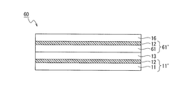
- FIG. 6 is a cross-sectional view showing a second configuration example of a gas barrier retardation film 60.
- FIG. 6 is a cross-sectional view showing a third configuration example of the gas barrier retardation film 60.
- FIG. 6 is a cross-sectional view illustrating a fourth configuration example of a gas barrier retardation film 60.
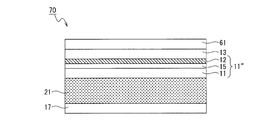
- FIG. 6 is a cross-sectional view showing a second configuration example of a gas barrier retardation film 70.
- FIG. 6 is a cross-sectional view showing a third configuration example of the gas barrier retardation film 70.
- FIG. 6 is a cross-sectional view illustrating a fourth configuration example of a gas barrier retardation film 70.
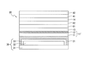
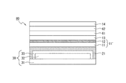
- FIG. It is sectional drawing which shows the 1st structural example of the organic electroluminescent display 80 which concerns on 6th Embodiment of this invention.
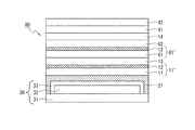
- 6 is a cross-sectional view showing a second configuration example of an organic EL display 80.
- FIG. It is sectional drawing which shows the structural example of the organic electroluminescent display which concerns on Example 2-1 of this invention. It is sectional drawing which shows the structural example of the organic electroluminescent display which concerns on the reference example 2.
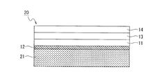
- FIG. 1 is a cross-sectional view showing a first configuration example of the gas barrier retardation film 10 according to the first embodiment of the present invention.
- the gas barrier retardation film 10 includes a retardation plate 11, an atomic layer deposition film 12 (ALD film), an adhesive layer 13, and a polarizing plate 14.
- the phase difference plate 11 is a transparent film that gives a predetermined phase difference to incident light.
- Examples of the phase difference plate 11 include a quarter wavelength plate or a combination of a quarter wavelength plate and a half wavelength plate.
- the retardation plate 11 includes a transparent uniaxially stretched polymer film such as polyvinyl alcohol, polycarbonate (PC), polysulfone, polystyrene, polyarylate, cycloolefin polymer (COP), cyclic olefin copolymer (COC), norbornene resin. Etc. can be used.
- the polymer film constituting the retardation plate 11 has a wavelength dependency of the refractive index, a single retardation plate 11 may not provide sufficient performance for light having a wide wavelength region. is there. For this reason, retardation films having different retardation values may be bonded to each other by shifting their optical axes to constitute a retardation plate 11 in which a half-wave plate and a quarter-wave plate are combined in a wide wavelength range. . Moreover, it is good also as a structure which combined the quarter wavelength plate and the isotropic base material.
- the atomic layer deposition film 12 is a film formed on the surface of the phase difference plate 11 by an ALD (Atomic Layer Deposition) method.
- the ALD method is a method in which a surface-adsorbed substance is formed one layer at a time by a chemical reaction on the surface.
- the ALD method alternately uses a gas rich in activity called a precursor or a precursor and a reactive gas, and alternately performs adsorption on the surface of the phase difference plate 11 and subsequent chemical reaction. In this way, the atomic layer is grown on the surface of the retardation plate 11 one by one.
- the ALD method can form a dense film with fewer film formation defects (that is, a film with excellent gas barrier properties) as compared with a vacuum deposition method, a sputtering method, or a general CVD method.
- a specific film formation method of the ALD method is performed by the following method.
- the self-limiting effect refers to a phenomenon in which, when the surface is adsorbed on the phase difference plate 11, if the surface is covered with a certain kind of gas, the gas is not further adsorbed.
- a reactive gas is introduced into the chamber to oxidize the precursor adsorbed on the surface of the phase difference plate 11 to form only one layer having a desired composition. Thereafter, the reactive gas is exhausted (second step).
- the first and second steps are defined as one cycle, and this cycle is repeated to form a thin film on the retardation plate 11 one by one at the atomic level.
- the atomic layer deposition film 12 contains a precursor (for example, a metal-containing precursor such as TMA: Tri-Methyl Aluminum or Tris-dimethylaminosilane) that is a raw material for the atomic layer deposition film 12.
- a precursor for example, a metal-containing precursor such as TMA: Tri-Methyl Aluminum or Tris-dimethylaminosilane
- the precursor located on the surface of the retardation plate 11 and the adsorption site of the retardation plate 11 are combined.
- an inorganic oxide film containing an element such as Al, Ti, Si, Zn, Sn, Ta, Nb, a nitride film or an oxynitride film containing these elements, or a mixed compound thereof is used. Can be used.
- the atomic layer deposition film 12 is made of AlSiOx, TiAlOx, TiOx, TaOx, or NbOx. Further, as the atomic layer deposition film 12, for example, an oxide film, a nitride film, an oxynitride film, a mixed compound thereof, or the like containing other elements (for example, Zr, Hf) can be used.
- the atomic layer deposition film 12 a film containing at least one element of Al, Si, and Ti (for example, a film as described above) is used from the viewpoints of water vapor barrier properties, durability, and cost. Good. By using a film containing such an element as the atomic layer deposition film 12, high water vapor barrier properties and high durability can be obtained, and costs can be reduced.
- the thickness of the atomic layer deposition film 12 is preferably not less than 0.5 nm and not more than 200 nm, for example. If the thickness of the atomic layer deposition film is less than 0.5 nm, an atomic layer deposition film having a sufficient water vapor barrier property cannot be formed from the viewpoint of manufacturing technology.
- the thickness of the atomic layer deposition film 12 exceeds 200 nm, it is not preferable because it requires cost and film formation time. Therefore, by setting the thickness of the atomic layer deposition film 12 within the range of 0.5 nm or more and 200 nm or less, the atomic layer deposition film 12 having a sufficient water vapor barrier property can be obtained in a short time.
- Adhesive layer 13 The adhesive layer 13 is provided between the retardation plate 11 and the polarizing plate 14, and has a function of bonding the retardation plate 11 and the polarizing plate 14.
- the adhesive layer 13 include a photo-curing adhesive resin, a thermosetting adhesive resin, a two-component curable adhesive resin made of an epoxy resin, an acrylic resin, a silicone resin, or an acid such as polyethylene or polypropylene.
- a method in which a thermoplastic adhesive resin made of a modified product or a main component having a hydroxyl group such as rubber, silicone, acrylic, or urethane is cured with an isocyanate curing agent is used.
- a laminating method for example, a gravure coater, a dip coater, a reverse coater, a wire bar coater, a die coater or the like can be used.
- the adhesion layer 13 may contain the curable moisture absorbent, respectively.
- the content ratio of the curable hygroscopic agent in the adhesive layer 13 is preferably 5% by mass or more and 60% by mass or less, more preferably 10% by mass or more and 45% by mass or less, when the total mass is 100% by mass. It is.
- the curable moisture absorbent is a mixture of a moisture absorbent and a curing agent.
- the content of the hygroscopic agent (compound) in the curable hygroscopic agent is preferably 20% by mass or more and 80% by mass or less, more preferably 25% by mass or more and 60% by mass or less when the total mass is 100% by mass. is there. When the content of the hygroscopic agent is within this range, the action of capturing moisture can be effectively expressed in the curable hygroscopic agent.
- the polarizing plate 14 is a transparent film laminated on the surface side of the retardation plate 11 with an adhesive layer 13 interposed therebetween.
- the polarizing plate 14 and the retardation plate 11 have a function of preventing reflection of external light, reflection of a background, and the like.
- the polarizing plate 14 is provided on the viewing side with respect to the retardation plate 11.
- the organic EL display is provided with a highly reflective metal layer (for example, an anode positioned between the TFT element and the organic EL layer), and has the polarizing plate 14 and the retardation plate 11 described above.
- the polarizing plate 14 for example, a film obtained by uniaxially stretching a film such as polyvinyl alcohol (PVA) on which a dichroic dye such as iodine is adsorbed and imparting polarization can be used.
- PVA polyvinyl alcohol
- the protective layer a structure sandwiched between optically isotropic films such as triacetyl cellulose (TAC) is used.
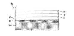
- FIG. 2 is a cross-sectional view showing a second configuration example of the gas barrier retardation film 10.
- the gas barrier phase difference film 10 may further include an undercoat layer 15 made of an inorganic material formed between the phase difference plate 11 and the atomic layer deposition film 12.
- the undercoat layer 15 may be disposed so as to cover the back surface of the retardation plate 11.
- the undercoat layer 15 is made of, for example, only an inorganic material.
- the undercoat layer 15 include SiOx, TaOx, or NbOx.
- the method for forming the undercoat layer 15 include a PVD method, a CVD method, and a sol-gel method.
- the inorganic material contained in the undercoat layer 15 has a larger number of adsorption sites (portions to which precursors that are raw materials for the atomic layer deposition film 12 are bonded) than the organic material. In general, an organic material is considered to have a mixed crystalline region and non-crystalline region.
- free volume there is a space where a polymer chain called free volume (free volume) does not exist, and gas diffuses and permeates through the space. Further, the gaseous precursor also passes through the free volume space until it is adsorbed on the adsorption site, and the dense film inherent to the atomic layer deposition method is not formed.
- an undercoat layer 15 containing an inorganic substance is provided on the retardation plate 11 in order to prevent the precursor from diffusing into the organic material.
- the gas containing the precursor cannot pass through the inorganic substance in the undercoat layer 15. This shortens the period from the start of the formation process of the atomic layer deposition film 12 to the formation of a dense film by two-dimensional growth.
- the thickness of the undercoat layer 15 is preferably, for example, 1 nm or more and 1000 nm or less.
- the thickness of the undercoat layer 15 is less than 1 nm, the surface of the phase difference plate 11 cannot be completely covered, the density of adsorption sites becomes insufficient, and the formation process of the atomic layer deposition film 12 starts. There is a possibility that the period until a dense film is formed by two-dimensional growth cannot be shortened. That is, the atomic layer deposition film 12 having a sufficient water vapor barrier property cannot be formed. On the other hand, if the thickness of the undercoat layer 15 exceeds 1000 nm, cost and film formation time are required, and further cracks and defects may occur in the undercoat layer 15, which may not be preferable.
- the undercoat layer 15 is disposed so as to cover the entire back surface of the retardation film 11 has been described as an example.
- the undercoat layer 15 may be disposed on at least a part of the back surface of the phase difference plate 11 and is not limited to the configuration shown in FIG.
- positioned so that the back surface of the phase difference plate 11 and the undercoat layer 15 might contact was mentioned as an example, and was demonstrated.
- an adhesion layer (not shown) may be disposed between the retardation film 11 and the undercoat layer 15.
- the adhesion layer is made of, for example, a resin layer containing an organic polymer. As described above, when the adhesion layer is provided between the retardation film 11 and the undercoat layer 15, the adhesion strength between the retardation film 11 and the undercoat layer 15 can be improved.
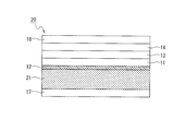
- FIG. 3 is a cross-sectional view illustrating a third configuration example of the gas barrier retardation film 10.
- the gas barrier retardation film 10 is an overcoat layer formed on the surface opposite to the surface facing the retardation plate 11 of the atomic layer deposition film 12 (the lower surface in FIG. 3). 16 may be further provided.
- the gas barrier retardation film 10 is formed so as to be peelable on the surface opposite to the surface facing the retardation plate 11 of the atomic layer deposition film 12 (the lower surface in FIG. 3). , May be further provided.
- FIG. 3 illustrates the case where the surface of the overcoat layer 16 is covered with the release film 17.
- the overcoat layer 16 is a protective film that protects the atomic layer deposition film 12.
- the overcoat layer 16 can prevent the atomic layer deposition film 12 from being damaged during the processing or transportation of the gas barrier retardation film, thereby impairing the barrier property.
- the overcoat layer 16 may be a layer containing an inorganic material similar to the undercoat layer 15 or may be a layer containing an organic material.
- the overcoat layer 16 can be formed by, for example, a PVD method or a CVD method when an inorganic material is included.
- an organic material when an organic material is included, it can be formed by, for example, a bar coating method, a spin coating method, a spray coating method, a die coating method, or the like.
- a sheet-like overcoat layer 16 may be laminated.
- the overcoat layer 16 may be a layer obtained by dry laminating a plastic film.
- the release film 17 is a protective film that protects the surface of the atomic layer deposition film 12 opposite to the surface facing the phase difference plate 11. It is possible to prevent the atomic layer deposition film 12 from being damaged and the barrier property from being damaged, or the overcoat layer 16 from being damaged and the optical properties from being damaged during the processing or transportation of the gas barrier retardation film.
- the release film 17 covers and protects the surface of the overcoat layer 16.
- the release film 17 has a base material and an adhesive provided on one surface of the base material. The adhesive of the release film 17 is adhered to a protective film such as the atomic layer deposition film 12 or the overcoat layer 16.
- the substrate may be paper or a resin film.
- the paper include fine paper and kraft paper.
- the resin film include a polyethylene terephthalate (PET) film.
- the pressure-sensitive adhesive may be a silicone-based pressure-sensitive adhesive containing silicone or a non-silicone-based pressure-sensitive adhesive not containing silicone.
- FIG. 4 is a cross-sectional view showing a fourth configuration example of the gas barrier retardation film 10.
- Hard coat layer 18 As shown in FIG. 4, the gas barrier retardation film 10 further includes a hard coat layer 18 formed on the surface opposite to the surface facing the retardation plate 11 of the polarizing plate 14 (upper surface in FIG. 4). You may have. The upper surface of the polarizing plate 14 is protected by the hard coat layer 18 formed on the upper surface of the polarizing plate 14.
- a material used for the hard coat layer 18 a material having visible light permeability can be used.
- various transparent resins such as acrylic resins such as acrylic esters, acrylamides, methacrylic esters, and methacrylamides, organic silicon resins, and thermosetting polysiloxane resins are used as the material of the hard coat layer 18. It's okay.
- the hard coat layer 18 can be formed by a thin film forming method corresponding to the material for forming the hard coat layer 18.
- the hard coat layer 18 is prepared by, for example, dissolving a resin as described above, which is a main component, and a material that absorbs ultraviolet rays in a solvent to prepare a coating solution, and using this coating solution as a die coater, curtain flow coater, or roll coater.
- a reverse roll coater, a gravure coater, a knife coater, a bar coater, a spin coater, a micro gravure coater or the like may be applied to the retardation plate 11 and the coating film may be cured by irradiation with ultraviolet rays or the like.
- the thickness of the hard coat layer 18 is, for example, 1 ⁇ m or more and 10 ⁇ m or less. However, the thickness of the hard coat layer 18 is not limited to this range. Further, the hard coat layer 18 may be provided on both surfaces of the polarizing plate 14. Although not shown, the gas barrier retardation film 10 may further include a release film that covers the upper surface of the hard coat layer 18. This release film may have the same composition as the release film 17 shown in FIG.
- the atomic layer deposition film 12 is formed on the back surface of the retardation film 11 (the lower surface in FIG. 4), and then the overcoat layer 16 is formed. .
- a polarizing plate 14 is attached to the surface of the retardation plate 11 (the upper surface in FIG. 4) via an adhesive layer 13, and a hard coat layer 18 is formed on the polarizing plate 14. To do.
- FIG. 5 is a cross-sectional view showing a fifth configuration example of the gas barrier retardation film 10.
- the gas barrier retardation film 10 may further include a hard coat layer 19 formed between the retardation plate 11 and the undercoat layer 15.
- the hard coat layer 19 is formed on the lower surface of the retardation plate 11 to improve the mechanical strength, abrasion resistance and the like of the retardation plate 11 and damage the retardation plate during processing and transportation. Can be prevented.
- the hard coat layer 19 may have the same composition as the hard coat of the polarizing plate 14 or a different composition. Moreover, the formation method may be the same or different.
- the hard coat layer 19 may be provided with antiglare properties and low reflectivity. It may be formed on both surfaces of the phase difference plate 11.
- Example of process order In the fifth configuration example, the hard coat layer 19 is formed on the back surface of the retardation plate 11 (the lower surface in FIG. 5), and then the undercoat layer 15 is formed. Further, an atomic layer deposition film 12 is formed. Before and after this, the polarizing plate 14 is attached to the surface of the retardation plate 11 (the upper surface in FIG. 5) via the adhesive layer 13.
- the first embodiment of the present invention has the following effects.
- the atomic layer deposition film 12 is a single thin film layer and has a high barrier property (10 ⁇ 4 to 10 ⁇ 6 g / (m 2 ⁇ day)). For this reason, the gas barrier layer in the gas barrier retardation film can be made thin (or the number of layers can be reduced), which leads to process reduction and cost reduction.
- the undercoat layer 15 has the effect of increasing the adsorption sites of the precursor that forms the atomic layer deposition film 12. Efficient and dense film formation is possible compared to forming the film directly on the phase difference plate 11. It is preferable to adjust the difference in refractive index with the atomic layer deposition film 12, and in that case, the optical characteristics can be maintained high.
- a laminated structure of a polarizing plate / retardation plate / adhesive layer / barrier film is assumed as a comparative example.
- two layers (adhesive layer, barrier film) of the laminated structure according to this comparative example are replaced with the atomic layer deposition film 12, so that the number of laminated gas barrier retardation films is reduced. Can do. Thereby, the process reduction of a gas-barrier phase difference film, cost reduction, and the improvement of a light transmittance can be aimed at.
- the water vapor permeability of the gas barrier retardation film 10 can be, for example, 0.01 g / (m 2 ⁇ day) or less.
- the gas-barrier phase difference film 10 can be used as a protective film of electronic members, such as an organic EL element.
- FIG. 6 is a cross-sectional view showing a first configuration example of a gas barrier retardation film 20 according to the second embodiment of the present invention.
- the gas barrier retardation film 20 includes a retardation plate 11, an atomic layer deposition film 12 (ALD film), an adhesive layer 13, a polarizing plate 14, and an atomic layer deposition film 12. And an adhesive layer 21 formed on the surface opposite to the surface facing the phase difference plate 11 (the lower surface in FIG. 6).
- FIG. 6 illustrates the case where the adhesive layer 21 is directly formed on the lower surface of the atomic layer deposition film 12, the adhesive layer is formed on the sealing layer when bonded to the organic EL element described later.
- An adhesive layer may be formed on the sealing layer side as long as the gas barrier phase difference film can be bonded through the film.
- the pressure-sensitive adhesive layer 21 may be a pressure-sensitive adhesive sheet or a layer coated with a pressure-sensitive adhesive. Moreover, although the kind of the adhesion layer 21 is not particularly limited, for example, an adhesive or an adhesive sheet described below can be used as the adhesion layer 21.
- Pressure-sensitive adhesive used as pressure-sensitive adhesive layer 21 examples include, for example, a photocurable adhesive resin made of epoxy resin, acrylic resin, silicone resin, or thermosetting adhesive. Resin, two-component curable adhesive resin, thermoplastic adhesive resin made of acid-modified products such as polyethylene and polypropylene, and isocyanate curing agent as the main component with hydroxyl groups such as rubber, silicone, acrylic and urethane The method of hardening with is mentioned. Among these, one obtained by polymerizing and curing one-component or two-component reactive polyurethane resin and trifunctional isocyanate is preferable.
- the processing is preferably a dry laminating method.
- As the coating method for example, a gravure coater, a dip coater, a reverse coater, a wire bar coater, a die coater or the like can be used.
- the pressure-sensitive adhesive used for the pressure-sensitive adhesive layer 21 may contain a hygroscopic agent or a curable hygroscopic agent.
- the curable moisture absorbent is a mixture of a moisture absorbent and a curing agent.
- the content of the hygroscopic agent (compound) in the curable hygroscopic agent is preferably 20% by mass or more and 80% by mass or less, more preferably 25% by mass or more and 60% by mass or less when the total mass is 100% by mass. is there. When the content ratio of the hygroscopic agent is within the above range, the action of capturing moisture can be effectively expressed in the curable hygroscopic agent.
- the hygroscopic agent according to this embodiment may contain an organometallic compound having a structural unit represented by the following general formula (i). -[Al (OR) -O] n- (i)
- R represents a substituted or unsubstituted alkyl group, aryl group or alkylcarbonyl group.
- n represents an integer of 2 to 6.
- a plurality of R may be the same or different, and may have a linear, cyclic or branched chain.
- the carbon number of R is preferably 5 to 30, more preferably 6 to 20, and particularly preferably 7 to 18.
- One of the functions of the compound having the structural unit represented by the general formula (1) is that the Al—OR bond present in the compound reacts with moisture to absorb moisture. By using such a compound, a hygroscopic agent excellent in hygroscopic performance can be obtained.
- thermosetting agent a thermosetting agent or an ultraviolet curing agent can be used.
- the thermosetting agent contains a curable monomer and an initiator.
- the curable monomer is not particularly limited as long as it is a compound having translucency and having one or more polymerizable reactive groups in the molecule. Examples of such a polymerizable reactive group include a (meth) acryloyl group, a vinyl group, and a vinyl ether group, and a (meth) acryloyl group is more preferable.
- the initiator is not particularly limited as long as it can be decomposed by heating to generate active species capable of polymerizing the above curable monomer.
- the ultraviolet curing agent includes a translucent monomer and a photopolymerization initiator.
- the translucent monomer for example, a monofunctional to trifunctional or higher polyfunctional acrylate (acrylic acid ester) or a monofunctional to trifunctional or higher polyfunctional methacrylate (methacrylic acid ester) can be used.
- acrylate and a methacrylate only any one may be used and you may mix and use it suitably.
- the photopolymerization initiator is preferably colorless and transparent, but it may be added in an amount of 1 to 3% by mass. Therefore, even if there is a color, there is no particular problem because the cured product obtained after ultraviolet irradiation becomes transparent.
- the pressure-sensitive adhesive sheet used as the pressure-sensitive adhesive layer 21 may be either a single layer or a laminated structure.
- an adhesive sheet having a structure in which a first organic sheet layer, a hygroscopic substance, and a second organic sheet layer are laminated may be used as the adhesive layer 21.
- each of the 1st organic sheet layer and the 2nd organic sheet layer may be formed with the hardened
- the thicknesses of the first organic sheet layer and the second organic sheet layer are preferably thicker (larger) than the particle diameter (average particle diameter) of the hygroscopic substance.
- each of the values of the film thickness of the first organic sheet layer and the film thickness of the second organic sheet layer is preferably set to a value equal to or greater than the average particle diameter of the hygroscopic substance. If each value of the film thickness of the first organic sheet layer and the film thickness of the second organic sheet layer is a value equal to or larger than the average particle diameter of the hygroscopic substance, the hygroscopic property is produced during the production of the organic EL display described later. The possibility that the substance presses the cathode of the organic EL element can be reduced, and the possibility that a part of the cathode is pushed by the hygroscopic substance to come into contact with the anode (that is, short-circuit) can be reduced.
- the first organic sheet layer and the second organic sheet layer may have the same thickness or different thicknesses.
- the thickness of the first organic sheet layer is thicker than the thickness of the second organic sheet layer. (That is, the thickness of the first organic sheet layer> the thickness of the second organic sheet layer) is desirable. This is likely to further reduce the possibility that the hygroscopic substance presses the cathode of the organic EL element.
- a chemical hygroscopic substance or a physical hygroscopic substance can be used as the hygroscopic substance sandwiched between the first organic sheet layer and the second organic sheet layer. More specifically, the hygroscopic substance may be a hygroscopic substance containing at least one of a chemical hygroscopic substance and a physical hygroscopic substance.
- Examples of the chemical hygroscopic substance include diphosphorus pentoxide (P 2 O 5 ), calcium oxide (CaO), and barium oxide (BaO).
- Examples of the physical hygroscopic substance include aluminum oxide (Al 2 O 3 ), zeolite (alumina silicate), silica gel, activated alumina, and the like.
- the particle diameter (average particle diameter) of the hygroscopic substance is 0.01 to 1000 ⁇ m, desirably 0.1 to 100 ⁇ m.
- the content of the hygroscopic substance is 1 to 90% by mass, preferably 15 to 65% by mass.
- One or several types of chemical hygroscopic substances can be used.
- one or several physical hygroscopic substances can be used.
- the first organic sheet layer and the second organic sheet layer preferably do not transmit water vapor as much as possible, and the water vapor transmission rate is desirably less than 10 g / (m 2 ⁇ day). Even if water vapor enters the first organic sheet layer and the second organic sheet layer, the water vapor is embedded in the first organic sheet layer and the second organic sheet layer. To absorb moisture.
- a product that can be used as the adhesive layer 21 is illustrated below.
- the adhesion layer 21 is not limited to the following commercial items. ⁇ Siden Chemical Co., Ltd. “OC-3405” ⁇ Mitsui Chemicals Co., Ltd. “XMF-T” ⁇ Mitsubishi Gas Chemical Co., Ltd. “Maxive” ⁇ Tesa “61500 ⁇ 61501” -Daicel Corporation “CELVENUS” ⁇ Sekisui Chemical Co., Ltd. “Photorec E” ⁇ DIC Corporation "PASLIM"
- FIG. 7 is a cross-sectional view showing a second configuration example of the gas barrier retardation film 20.
- the gas barrier phase difference film 20 may further include an undercoat layer 15 made of an inorganic material formed between the phase difference plate 11 and the atomic layer deposition film 12.
- the undercoat layer 15 is formed on the back surface of the retardation plate 11 (the lower surface in FIG. 7), then the atomic layer deposition film 12 is formed, and then the adhesive layer 21 is formed. .
- the polarizing plate 14 is bonded to the surface of the retardation plate 11 (the upper surface in FIG. 7) via the adhesive layer 13.
- FIG. 8 is a cross-sectional view illustrating a third configuration example of the gas barrier retardation film 20.
- the gas barrier retardation film 20 is an overcoat layer formed on the surface opposite to the surface facing the retardation plate 11 of the atomic layer deposition film 12 (the lower surface in FIG. 8). 16 may be further provided.
- the gas barrier film further includes a release film 17 formed so as to be peelable on the surface opposite to the surface facing the phase difference plate 11 of the atomic layer deposition film 12 (the lower surface in FIG. 8). You may prepare. In FIG. 8, the case where the peeling film 17 has covered the surface of the adhesion layer 21 is illustrated.
- the undercoat layer 15 is formed on the back surface of the retardation plate 11 (the lower surface in FIG. 8), then the atomic layer deposition film 12 is formed, and then the overcoat layer 16 is formed. Further, the adhesive layer 21 is formed, and then the release film 17 is attached to the adhesive layer 21. Before and after this, the polarizing plate 14 is attached to the surface of the retardation plate 11 (the upper surface in FIG. 8) via the adhesive layer 13.
- FIG. 9 is a cross-sectional view illustrating a fourth configuration example of the gas barrier retardation film 20.
- the gas barrier retardation film 20 further includes a hard coat layer 18 formed on the surface opposite to the surface facing the retardation plate 11 of the polarizing plate 14 (the upper surface in FIG. 9). You may have.
- the upper surface of the polarizing plate 14 is protected by the hard coat layer 18 formed on the upper surface of the polarizing plate 14.
- the hard coat layer 18 may have hard coat properties, antiglare properties, low reflectivity, and the like.
- the gas barrier retardation film 20 may further include a release film 17 that covers the upper surface of the hard coat layer 18.
- the atomic layer deposition film 12 is formed on the back surface (the lower surface in FIG. 9) of the retardation plate 11, the adhesive layer 21 is further formed, and then the release film 17 is formed on the adhesive layer 21. Affix. Before and after this, a polarizing plate 14 is attached to the surface of the retardation plate 11 (the upper surface in FIG. 9) via an adhesive layer 13, and a hard coat layer 18 is formed on the polarizing plate 14. To do.
- FIG. 10 is a cross-sectional view showing a fifth configuration example of the gas barrier retardation film 20.
- the gas barrier retardation film 20 may further include a hard coat layer 19 formed between the retardation plate 11 and the undercoat layer 15.
- the hard coat layer 19 is formed on the lower surface of the retardation plate 11 and improves the mechanical strength, abrasion resistance, and the like of the retardation plate 11.
- the hard coat layer 19 is formed on the back surface of the retardation plate 11 (the lower surface in FIG. 10), then the undercoat layer 15 is formed, and then the atomic layer deposition film 12 is formed. Further, an adhesive layer 21 is formed. Before and after this, the polarizing plate 14 is attached to the surface of the retardation film 11 (the upper surface in FIG. 10) via the adhesive layer 13.
- the second embodiment has the same effects as the first embodiment. Moreover, in addition to the effect of 1st Embodiment, there exist the following effects.
- (6.1) The pressure-sensitive adhesive layer 21 is already formed on the gas barrier retardation film 20. For this reason, it is not necessary for a panel manufacturer or the like to apply an adhesive or attach an adhesive sheet in order to attach the gas barrier retardation film 20 to the organic EL element.
- the pressure-sensitive adhesive layer 21 functions as a protective layer for protecting the atomic layer deposition film 12 until immediately before bonding to the organic EL element (for example, during transportation), and also functions as an adhesive layer when bonding the organic EL element. . Therefore, it is possible to reduce processes in panel manufacturers and the like.
- the pressure-sensitive adhesive layer 21 has a barrier property, end face leakage from the side surface side of the organic EL element can be suppressed.
- the organic EL element is likely to be deteriorated due to the influence of moisture and oxygen in the atmosphere.
- the adhesive layer 21 covers the organic EL element, thereby preventing moisture from entering from the outside.
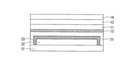
- FIG. 11 is a cross-sectional view showing a first configuration example of an organic EL display 50 according to the third embodiment of the present invention.
- the organic EL display 50 includes the gas barrier retardation film 10 (excluding the release film 17) described in the first embodiment, the organic EL element 30, the organic EL element 30, and the gas barrier.
- the adhesive layer 21 which adheres the adhesive phase difference film 10 is provided.
- the organic EL display 50 may include the gas barrier retardation film 20 described in the second embodiment, and the organic EL element 30 attached to the adhesive layer 21 side of the gas barrier retardation film 20. .
- the organic EL element 30 includes a support substrate 31, an element body 32 formed on one surface of the support substrate 31 (upper surface in FIG. 11), and an element body 32 formed on one surface of the support substrate 31. And a sealing layer 33 that seals.
- the sealing layer 33 is made of an inorganic film, for example.
- the element body 32 has a structure in which a TFT element, an anode, an organic EL layer, and a cathode are laminated in this order from the support substrate 31 side.
- the sealing layer 33 of the organic EL element 30 is on the surface side closer to the retardation plate 11 than the polarizing plate 14 on both surfaces of the gas barrier retardation film. It is attached.
- the surface and side surfaces of the sealing layer 33 are covered with the adhesive layer 21.
- the organic EL display 50 may further include a cover glass 42 attached to the polarizing plate 14 via the adhesive layer 41 as a part of a gas barrier retardation film, for example. .
- this organic EL display 50 may further be provided with the touchscreen layer provided in the surface side which faces the adhesion layer 41 of the cover glass 42, for example as a part of gas-barrier phase difference film. Below, the adhesion layer 41, the cover glass 42, and a touch panel layer are demonstrated.
- Adhesive layer 41 The adhesive layer 41 is provided between the polarizing plate 14 and the cover glass, and has a function of bonding the polarizing plate 14 and the cover glass 42.
- a photo-curing adhesive resin for example, a thermosetting adhesive resin, a two-component curable adhesive resin made of an epoxy resin, an acrylic resin, a silicone resin, or the like, or an acid such as polyethylene or polypropylene is used.
- a method in which a thermoplastic adhesive resin made of a modified product or a main component having a hydroxyl group such as rubber, silicone, acrylic, or urethane is cured with an isocyanate curing agent is used.
- the processing is preferably a dry laminating method, and as a coating method, for example, a gravure coater, a dip coater, a reverse coater, a wire bar coater, a die coater or the like can be used.
- the adhesive layer 41 may contain a curable hygroscopic agent.
- the content of the curable hygroscopic agent in the adhesive layer 41 is preferably 5% by mass or more and 60% by mass or less, more preferably 10% by mass or more and 45% by mass or less, when the total mass is 100% by mass. It is.
- the curable moisture absorbent is a mixture of a moisture absorbent and a curing agent.
- the content of the hygroscopic agent (compound) in the curable hygroscopic agent is preferably 20% by mass or more and 80% by mass or less, more preferably 25% by mass or more and 60% by mass or less when the total mass is 100% by mass. is there. When the content of the hygroscopic agent is within this range, the action of capturing moisture can be effectively expressed in the curable hygroscopic agent.
- the cover glass 42 is a front plate serving as the outermost surface, and is made of aluminosilicate glass containing at least one alkali metal oxide selected from SiO 2 , Al 2 O 3 , Li 2 O, and Na 2 O. A reinforced treatment is used. Moreover, the cover glass 42 may be comprised with the resin base material.
- Touch Panel Layer A touch panel sensor included in the touch panel layer has a lead-out wiring, two transparent electrodes for X direction and Y direction, and an insulating layer between the two transparent electrodes. The touch panel layer including the touch panel sensor is attached to the cover glass 42 via, for example, a transparent adhesive sheet (OCA).
- OCA transparent adhesive sheet
- the arrangement position of the touch panel layer is not limited to the above, and may be provided anywhere on the sealing layer 33 (FIGS. 11 to 13) and below the cover glass.
- FIG. 12 is a cross-sectional view showing a second configuration example of the organic EL display 50.
- the atomic layer deposition film 12 may be formed not between the retardation plate 11 and the adhesive layer 21 but between the retardation plate 11 and the adhesive layer 13. That is, the atomic layer deposition film 12 may be formed not on the back surface of the phase difference plate 11 but on the front surface.
- FIG. 13 is a cross-sectional view showing a third configuration example of the organic EL display 50.
- the atomic layer deposition film 12 may be formed between the retardation plate 11 and the adhesive layer 21 and between the retardation plate 11 and the adhesive layer 13. That is, the atomic layer deposition film 12 may be formed on both surfaces of the phase difference plate 11.
- the third embodiment has the same effects as the first and second embodiments. In addition to the effects of the first and second embodiments, the following effects are achieved.
- (4.1) In order to further promote the spread of the organic EL display 50, there is a demand for a reduction in production cost and a reduction in the number of processes. For example, when the sealing layer 33 has a laminated structure, the greater the number of laminated layers, the larger the number of steps, which increases the manufacturing cost. For example, when the sealing layer 33 has a three-layer structure of inorganic layer (SiN) / organic layer / inorganic layer (SiN), it is necessary to form these three layers by the CVD method or the like, and the number of steps is large.
- the atomic layer deposition film 12 having a high gas barrier property even though it is thin is used for the gas barrier retardation film covering the sealing layer 33.
- the number of layers of the sealing layer 33 can be reduced, and the number of steps can be reduced.
- the number of steps of the organic EL display 50 can be reduced, and the production cost can be reduced.
- the retardation plate 11 and the polarizing plate 14 are necessary for the organic EL display 50.
- the organic EL display 50 in which these layers are laminated tends to be thick.
- membrane 12 as a gas barrier layer of a gas barrier phase difference film. For this reason, it is possible to reduce the number of laminated sealing layers while maintaining the gas barrier property of the organic EL display, and it is possible to shorten the passage distance of light emitted from the organic EL element. Therefore, the organic EL display 50 can be thinned and the light transmittance can be improved.
- FIG. 14 is a cross-sectional view showing a configuration example of an organic EL display according to Example 1-1 of the present invention.
- the organic EL display according to Example 1-1 includes an organic EL element (supporting substrate 31, element body 32, and sealing layer 33) and a gas barrier retardation film (retardation plate 11, atomic plate).
- a layer deposition film 12 an adhesive layer 13 and a polarizing plate 14
- an adhesive layer 21 for joining the organic EL element and the gas barrier retardation film.
- FIG. 15 is a cross-sectional view illustrating a configuration example of an organic EL display according to Reference Example 1.
- the organic EL display according to Reference Example 1 includes an organic EL element (support substrate 31, element body 32 and sealing layer 330) and a gas barrier retardation film (retardation plate 11, adhesive layer 13). And a polarizing plate 14), and an adhesive layer 21 for joining the organic EL element and the gas barrier retardation film.
- the sealing layer 330 is a film having a three-layer structure in which an inorganic layer 331, an organic layer 332, and an inorganic layer 333 are stacked in this order.
- Example 1-2 differs from Example 1-1 in that an undercoat layer 15 is provided between the phase difference plate 11 and the atomic layer deposition film 12. Further, the difference between the comparative example 1 and the reference example 1 is that the sealing layer is not a three-layer structure but only one layer of SiNx. Table 1 shows the evaluation results of Examples 1-1 and 1-2, Comparative Example 1 and Reference Example 1 performed by the inventors.
- Element deterioration tolerance rate (area of black spots generated in elements not subjected to accelerated deterioration processing / area of black spots generated in elements subjected to accelerated deterioration processing) ⁇ 100 (%) (ii) A: The element deterioration resistance rate is 90% or more. A: The element deterioration resistance rate is 60% or more and less than 90%. ⁇ : The element deterioration resistance rate is 20% or more and less than 60%. X: The element deterioration resistance rate is less than 20%.
- FIG. 16 is a cross-sectional view showing a first configuration example of a gas barrier retardation film 60 according to the fourth embodiment of the present invention.
- the gas barrier retardation film 60 includes a retardation plate (first retardation plate) 11, an atomic layer deposition film 12 that is an atomic deposition layer, an adhesive layer 13, and a retardation plate. (Second retardation plate) 61 are provided in this order.
- the first retardation plate 11 and the second retardation plate 61 are transparent films that give a predetermined phase difference to incident light, and have different phase differences from each other.
- a 1 ⁇ 4 wavelength plate or a 1 ⁇ 2 wavelength plate is exemplified.
- the first retardation plate 11 and the second retardation plate 61 include transparent uniaxially stretched polymer films such as polyvinyl alcohol (PVA), polycarbonate (PC), polysulfone (PSF), polystyrene (PS), poly Arylate (PAR), cycloolefin polymer (COP), cyclic olefin copolymer (COC), norbornene resin, and the like can be used.
- PVA polyvinyl alcohol
- PC polycarbonate
- PSF polysulfone
- PS polystyrene
- PAR poly Arylate
- COP cycloolefin polymer
- COC cyclic olefin copolymer
- norbornene resin and the like can be used.
- a retardation plate is formed by combining a half-wave plate and a quarter-wave plate in a wide wavelength range. For example, an example in which a 1 ⁇ 4 wavelength plate is used for the first retardation plate 11 and a 1 ⁇ 2 wavelength plate is used for the second retardation plate 61 is shown.
- the atomic layer deposition film 12 is a film formed on the surface of the first retardation plate 11 or the second retardation plate 61 by the ALD method.
- the atomic layer deposition film 12 of the present embodiment has the same configuration as the atomic layer deposition film 12 described in the first embodiment. Therefore, detailed description thereof is omitted here.
- Adhesive layer 13 The adhesive layer 13 is provided between the first phase difference plate 11 and the second phase difference plate 61, and has a function of bonding the first phase difference plate 11 and the second phase difference plate 61. Have.
- the adhesive layer 13 of the present embodiment has the same configuration as the adhesive layer 13 described in the first embodiment. Therefore, detailed description thereof is omitted here.
- the adhesive layer 13 may contain a curable hygroscopic material.
- the content of the curable hygroscopic material in the adhesive layer 13 is preferably 5% by mass or more and 60% by mass or less, more preferably 10% by mass or more and 45% by mass or less, when the total mass is 100% by mass. It is. When the content of the hygroscopic agent is within this range, the effect of rehydrating water can be effectively expressed in the curable hygroscopic agent.
- the atomic layer deposition film 12 is formed on the surface of the first retardation plate 11 (the upper surface in FIG. 16), and the gas barrier retardation plate 11 ′.
- the second retardation plate 61 is bonded to the surface of the gas barrier retardation plate 11 ′ on which the atomic layer deposition film 12 is formed via the adhesive layer 13.
- the first retardation plate 11 uses a 1 ⁇ 4 wavelength plate
- the second retardation plate 61 uses a 1 ⁇ 2 wavelength plate.
- FIG. 17 is a cross-sectional view showing a second configuration example of the gas barrier retardation film 60.
- the gas barrier phase difference film 60 of the second configuration example is formed on the atomic layer deposition film 12 formed on the first phase difference plate 11 and the second phase difference plate 61. And an atomic layer deposition film 12.
- the gas barrier retardation film 60 has an overcoat layer 16 formed on the surface opposite to the surface facing the second retardation plate 61 of the atomic layer deposition film 12 (the upper surface in FIG. 17). Further prepare.
- the overcoat layer 16 is a protective film that protects the atomic layer deposition film 12.
- the overcoat layer 16 of the present embodiment has the same configuration as the overcoat layer 16 described in the first embodiment. Therefore, detailed description thereof is omitted here.
- an inorganic material for example, TiOx, AlOx, or ZrOx may be used as the inorganic material in addition to the SiOx, TaOx, or NbOx described in the first embodiment. .
- the atomic layer deposition film 12 is formed on the surface of the first retardation plate 11 (upper surface in FIG. 17), and the gas barrier retardation plate 11 ′. And Next, an atomic layer is formed on the surface (the upper surface in FIG. 17) of the second retardation plate 61 via the adhesive layer 13 on the surface of the gas barrier retardation plate 11 ′ on which the atomic layer deposition film 12 is formed. A gas barrier phase difference plate 61 ′ on which the deposited film 12 is formed is bonded. Further, the overcoat layer 16 is formed on the surface of the gas barrier retardation plate 61 ′ on which the atomic layer deposition film 12 is formed. At this time, the first retardation plate 11 uses a 1 ⁇ 4 wavelength plate, and the second retardation plate 61 uses a 1 ⁇ 2 wavelength plate.
- FIG. 18 is a cross-sectional view showing a third configuration example of the gas barrier retardation film 60.
- the gas barrier phase difference film 60 of the third configuration example includes an undercoat layer 15 made of an inorganic material formed between the first phase difference plate 11 and the atomic layer deposition film 12. Further prepare.
- the undercoat layer 15 may be disposed so as to cover the surfaces of the first retardation plate 11 and the second retardation plate 61.
- the undercoat layer 15 is a retardation plate (the first retardation plate 11 or the second retardation plate) in order to prevent the precursor used in forming the atomic layer deposition film 12 from diffusing into the organic material. 61) A layer provided on top.
- the undercoat layer 15 of the present embodiment has the same configuration as the undercoat layer 15 described in the first embodiment. Therefore, detailed description thereof is omitted here.
- an inorganic material for example, TiOx, AlOx, or ZrOx may be used as the inorganic material in addition to the SiOx, TaOx, or NbOx described in the first embodiment. .
- TiOx, AlOx, or ZrOx may be used as the inorganic material in addition to the SiOx, TaOx, or NbOx described in the first embodiment. .
- the undercoat layer 15 is disposed so as to cover the entire surface of the first retardation plate 11 has been described as an example.
- the undercoat layer 15 may be disposed on at least a part of the surface of the first retardation plate 11, and is not limited to the configuration shown in FIG.
- the undercoat layer 15 is arranged so that the surface of the first retardation plate 11 and the undercoat layer 15 are in contact with each other has been described as an example.
- an adhesion layer (not shown) may be disposed between the first retardation plate 11 and the undercoat layer 15.
- the adhesion layer is made of, for example, a resin layer containing an organic polymer. As described above, when the adhesion layer is provided between the first retardation plate 11 and the undercoat layer 15, the adhesion strength between the first retardation plate 11 and the undercoat layer 15 can be improved.
- the undercoat layer 15 is formed on the surface of the first retardation plate 11 (upper surface in FIG. 18), and then the atomic layer deposition film 12 is formed. To form a gas barrier phase difference plate 11 ′′.
- the second retardation plate 61 is bonded to the surface of the gas barrier retardation plate 11 ′′ on which the atomic layer deposition film 12 is formed via the adhesive layer 13.
- the first retardation plate 11 uses a 1 ⁇ 4 wavelength plate
- the second retardation plate 61 uses a 1 ⁇ 2 wavelength plate.
- FIG. 19 is a cross-sectional view illustrating a fourth configuration example of the gas barrier retardation film 60.
- the gas barrier retardation film 60 of the fourth configuration example has a polarizing plate 14 on the surface of the second retardation plate 61 (the upper surface in FIG. 19) via an adhesive layer 62. Is further provided.
- the polarizing plate 14 is a transparent film laminated on the surface side of the second retardation plate 61 via an adhesive layer 62.
- the polarizing plate 14 of the present embodiment has substantially the same configuration as the polarizing plate 14 described in the first embodiment.
- the adhesive layer 62 of the present embodiment has substantially the same configuration as the adhesive layer 13 described in the first embodiment. Therefore, detailed description thereof will be omitted here.
- the polarizing plate 14 has a function of converting incident light into linearly polarized light, and a configuration in which the polarizing plate 14 and a quarter retardation plate are bonded together is referred to as a circularly polarizing plate.
- the light incident on the polarizing plate 14 becomes linearly polarized light, and the linear change incident on the 1 ⁇ 4 phase difference plate becomes circularly polarized light.
- Circularly polarized light is reflected as reverse circularly polarized light, and the reflected light is absorbed by the polarizing plate.
- a highly reflective metal plate (for example, an anode positioned between the TFT element and the organic EL layer) is provided inside the organic EL display. The reflected light can be removed.
- the retardation plate used for the circularly polarizing plate is composed of a polymer film
- the polymer film has a wavelength dependency of the refractive index. Therefore, sufficient antireflection performance may not be obtained with only one type of retardation plate, for example, a quarter retardation plate, for light having a wide wavelength region. Therefore, a retardation film that functions in a wide wavelength region is obtained by laminating retardation films having different retardations while shifting their optical axes.
- the circularly polarizing plate having high antireflection performance is preferably laminated in the order of a linearly polarizing plate, a half-wave plate, and a quarter-wave plate as viewed from the viewing side.
- an atomic layer deposition film 12 is formed on the surface of the first retardation plate 11 (upper surface in FIG. 19) to form a gas barrier retardation plate 11 ′.
- the second retardation plate 61 is bonded to the surface of the gas barrier retardation plate 11 ′ on which the atomic layer deposition film 12 is formed via the adhesive layer 13.
- the polarizing plate 14 is bonded to the surface of the second retardation plate 61 opposite to the surface facing the atomic layer deposition film 12 (the upper surface in FIG. 19) via the adhesive layer 62.
- the first retardation plate 11 is a quarter wavelength plate
- the second retardation plate 61 is a half wavelength plate
- the polarizing plate 14 is a linear polarizing plate.
- the fourth embodiment of the present invention has the same effects as the first to third embodiments described above.
- the atomic layer deposition film 12 is a single thin film layer and has a high barrier property (10 ⁇ 4 to 10 ⁇ 6 g / (m 2 ⁇ day)). For this reason, the gas barrier film in the gas barrier retardation film can be thinned (or the number of layers can be reduced), which leads to process reduction and cost reduction.
- the undercoat layer 15 has an effect of increasing the adsorption sites of the precursor that forms the atomic layer deposition film 12. Therefore, it is possible to form a more efficient and dense film than directly forming a film on the phase difference plate (the first phase difference plate 11 or the second phase difference plate 61).
- the optical characteristics can be maintained high.
- it is a gas barrier phase difference film according to this embodiment and an organic EL display provided with the same, it has high gas barrier properties and high antireflection performance (particularly antireflection performance for light having a wide wavelength region), Further thinning may be possible.
- the atomic layer deposition film 12 is sandwiched between the first retardation plate 11 and the second retardation plate 61, the atomic layer deposition film 12 can be protected.
- the atomic layer deposition film 12 may be damaged during processing or transportation, and the barrier property may be impaired.
- the atomic layer deposition film 12 is easily handled by having a sandwich structure with the first retardation plate 11 and the second retardation plate 61. Will improve.
- the pressure-sensitive adhesive that bonds the first retardation plate 11 and the second retardation plate 61 also has a function as a buffer material, and the bending resistance of the atomic layer deposition film 12 is improved.
- each of the gas barrier phase difference plate 11 ′, the gas barrier phase difference plate 11 ′′ and the gas barrier phase difference plate 61 ′ is provided with a phase difference film having a different phase difference, the optical axis thereof is shifted. It has antireflection performance in a wide wavelength range.
- a laminated structure of retardation plate / adhesive layer / barrier film is assumed as a comparative example.
- two layers (adhesive layer / barrier film) in the laminated structure according to this comparative example are replaced with the atomic layer deposition film 12. Therefore, the number of laminated gas barrier retardation films can be reduced. Thereby, the process reduction of a gas-barrier phase difference film, cost reduction, and a light transmittance improvement can be aimed at.
- the water vapor transmission rate of the gas barrier retardation film 60 can be set to 0.01 g / (m 2 ⁇ day), for example.
- the gas-barrier retardation film 60 can be used as a protective film for electronic members such as organic EL elements.
- a gas barrier retardation film 70 according to a fifth embodiment of the present invention will be described with reference to a plurality of configuration examples.
- FIG. 20 is a cross-sectional view showing a first configuration example of a gas barrier retardation film 70 according to a fifth embodiment of the present invention.
- the gas barrier retardation film 70 includes a first retardation plate 11, an atomic layer deposition film 12, an adhesive layer 13, and a second retardation plate 61 in this order.
- the pressure-sensitive adhesive layer 21 is provided on the surface opposite to the surface facing the first retardation plate 11 of the atomic layer deposition film 12 (the lower surface in FIG. 20).
- Adhesive layer 21 The adhesive layer 21 of the present embodiment has the same configuration as the adhesive layer 21 described in the second embodiment. Therefore, detailed description thereof is omitted here.
- Adhesive used as adhesive layer 21 The adhesive used as adhesive layer 21 of this embodiment is the same structure as the adhesive used as adhesive layer 21 demonstrated in 2nd Embodiment.
- the hygroscopic agent, the curing agent, and the like added to the pressure-sensitive adhesive have the same configuration as the hygroscopic agent, the curing agent, and the like described in the second embodiment. Therefore, detailed description thereof will be omitted here.
- Adhesive sheet used as adhesive layer 21 The adhesive sheet used as adhesive layer 21 of this embodiment is the same structure as the adhesive sheet used as adhesive layer 21 demonstrated in 2nd Embodiment. Therefore, detailed description thereof is omitted here.
- An example of a product that can be used as the adhesive layer 21 The product that can be used as the adhesive layer 21 in this embodiment has the same configuration as the product that can be used as the adhesive layer 21 described in the second embodiment. . Therefore, detailed description thereof is omitted here.
- an atomic layer deposition film 12 is formed on the surface of the first retardation plate 11 (upper surface in FIG. 20) to form a gas barrier retardation plate 11 ′.
- an adhesive layer 21 is formed on the back surface (the lower surface in FIG. 20) of the gas barrier retardation plate 11 ′.
- the second retardation plate 61 is provided on the surface (the upper surface in FIG. 20) on which the atomic layer deposition film 12 of the gas barrier retardation plate 11 ′ is formed via the adhesive layer 13. Glue.
- FIG. 21 is a cross-sectional view showing a second configuration example of the gas barrier retardation film 70.
- the gas barrier phase difference film 70 of the second configuration example is formed on the atomic layer deposition film 12 formed on the first phase difference plate 11 and the second phase difference plate 61. And an atomic layer deposition film 12.
- the gas barrier retardation film 70 has an overcoat layer 16 formed on the surface opposite to the surface facing the second retardation plate 61 of the atomic layer deposition film 12 (the upper surface in FIG. 21). Further prepare.
- the atomic layer deposition film 12 is formed on the surface of the first retardation plate 11 (the upper surface in FIG. 21), and the adhesive layer 21 is attached to the back surface of the first retardation plate 11 (FIG. 21 on the lower surface).
- the second retardation film 61 is bonded to the surface of the first retardation film 11 on which the atomic layer deposition film 12 is formed via the adhesive layer 13.
- the atomic layer deposition film 12 is formed on the surface of the second retardation plate 61 (upper surface in FIG. 21), and further, the surface of the atomic layer deposition film 12 facing the second retardation plate 61 is formed.
- An overcoat layer 16 is formed on the opposite surface side.
- FIG. 22 is a cross-sectional view illustrating a third configuration example of the gas barrier retardation film 70.
- the gas barrier retardation film 70 of the third configuration example has an undercoat layer 15 made of an inorganic material formed between the first retardation plate 11 and the atomic layer deposition film 12. Further prepare.
- FIG. 22 illustrates the case where the release film 17 covers the surface of the adhesive layer 21.
- the undercoat layer 15 is formed on the surface of the first retardation plate 11 (the upper surface in FIG. 22), then the atomic layer deposition film 12 is formed, and the adhesive layer 21 is further formed. Is formed on the back surface (the lower surface in FIG. 22) of the first retardation plate 11, and then the release film 17 is attached to the adhesive layer 21. Next, the second retardation plate 61 is bonded to the surface of the first retardation plate 11 on which the atomic layer deposition film 12 is formed via the adhesive layer 13.
- FIG. 23 is a cross-sectional view illustrating a fourth configuration example of the gas barrier retardation film 70.
- the gas barrier retardation film 70 of the fourth configuration example has a polarizing plate 14 on the surface of the second retardation plate 61 (the upper surface in FIG. 23) via an adhesive layer 62. Is further provided.
- the atomic layer deposition film 12 is formed on the surface of the first retardation plate 11 (upper surface in FIG. 23), and the back surface of the first retardation plate 11 (in FIG. 23).
- the adhesive layer 21 is formed on the lower surface.
- the second retardation plate 61 is bonded to the surface of the first retardation plate 11 on which the atomic layer deposition film 12 is formed via the adhesive layer 13.
- the polarizing plate 14 is bonded to the surface of the second retardation plate 61 opposite to the surface facing the atomic layer deposition film 12 (the upper surface in FIG. 23) via the adhesive layer 62.
- the first retardation plate 11 is a quarter wavelength plate
- the second retardation plate 61 is a half wavelength plate
- the polarizing plate 14 is a linear polarizing plate.
- the fifth embodiment has the same effects as the fourth embodiment. Moreover, in addition to the effect of 4th Embodiment, there exist the following effects.
- the pressure-sensitive adhesive layer 21 is already formed on the gas barrier retardation film 70. For this reason, it is not necessary for a panel manufacturer or the like to apply an adhesive or attach an adhesive sheet in order to attach the gas barrier retardation film 70 to the organic EL element. Therefore, it is possible to reduce processes in panel manufacturers and the like.
- the adhesive layer 21 has a barrier property, end face leakage from the side surface of the organic EL element can be suppressed. For example, a material that easily deteriorates due to the influence of moisture and oxygen in the atmosphere is used for the organic EL element. By covering the organic EL element with the adhesive layer 21, it is possible to block moisture from entering from the outside. .
- FIG. 24 is a cross-sectional view showing a first configuration example of an organic EL display 80 according to the sixth embodiment of the present invention.
- this organic EL display 80 is bonded to the gas barrier retardation film 70, the organic EL element 30, and the organic EL element 30 and the gas barrier retardation film 70 described in the fourth embodiment.
- An adhesive layer 21 is provided.
- the organic EL display 80 may include the gas barrier retardation film 70 described in the fifth embodiment and the organic EL element 30 attached to the adhesive layer 21 side of the gas barrier retardation film 70.
- the organic EL element 30 of the present embodiment has the configuration of the organic EL element 30 described in the third embodiment. Therefore, detailed description thereof is omitted here.
- this organic EL display 80 the organic EL element 30 is disposed closer to the surface side closer to the first retardation plate 11 than the polarizing plate 14, out of both surfaces of the gas barrier retardation film 70.
- a sealing layer 33 is attached. The surface and side surfaces of the sealing layer 33 are covered with the adhesive layer 21.
- the organic EL display 80 may further include a cover glass 42 attached to the polarizing plate 14 via the adhesive layer 41 as a part of the gas barrier retardation film 70, for example. Moreover, although not shown in figure, this organic EL display 80 may further be provided with the touchscreen layer provided in the surface side facing the adhesion layer 41 of the cover glass 42 as a part of gas-barrier phase difference film 70, for example. . Below, the adhesion layer 41, the cover glass 42, and a touch panel layer are demonstrated.
- Adhesive layer 41 The adhesive layer 41 of this embodiment is provided between the polarizing plate 14 and the cover glass 42 and has a function of bonding the polarizing plate 14 and the cover glass 42.
- the adhesive layer 41 has the same configuration as the adhesive layer 41 described in the third embodiment. Therefore, detailed description thereof is omitted here.
- Cover glass 42 The cover glass 42 of the present embodiment has the same configuration as the cover glass 42 described in the third embodiment. Therefore, detailed description thereof is omitted here.
- Touch Panel Layer The touch panel layer including the touch panel sensor of the present embodiment has the same configuration as the touch panel layer including the touch panel sensor described in the third embodiment. Therefore, detailed description thereof is omitted here.
- FIG. 25 is a cross-sectional view showing a second configuration example of the organic EL display 80.
- the atomic layer deposition film 12 has a second phase difference between the first phase difference plate 11 and the second phase difference plate 61. It is formed between the plate 61 and the polarizing plate 14, respectively.
- the sixth embodiment has the same effects as the fourth and fifth embodiments. In addition to the effects of the fourth and fifth embodiments, the following effects can be obtained.
- (3.1) In order to further promote the spread of the organic EL display 80, there is a demand for a reduction in production cost and a reduction in the number of processes. For example, when the sealing layer 33 has a laminated structure, the greater the number of laminated layers, the larger the number of steps, which increases the manufacturing cost. For example, when the sealing layer 33 has a three-layer structure of inorganic layer (SiN) / organic layer / inorganic layer (SiN), it is necessary to form these three layers by the CVD method or the like, and the number of steps is large.
- the atomic layer deposition film 12 having a single thin film and high gas barrier properties is used for the gas barrier retardation film 70 covering the sealing layer 33.
- the number of layers of the sealing layer 33 can be reduced, and the number of steps can be reduced.
- the number of steps of the organic EL display 80 can be reduced, and the production cost can be reduced.
- the organic EL display 80 requires the first retardation plate 11, the second retardation plate 61, and the polarizing plate 14 to prevent internal reflection.
- An organic EL display in which these layers are laminated tends to be thick.
- the atomic layer deposition film 12 is provided as a gas barrier layer of the gas barrier retardation film 70. For this reason, it is possible to reduce the number of laminated sealing layers while maintaining the gas barrier property of the organic EL display, and it is possible to shorten the passage distance of light emitted from the organic EL display. Therefore, it is possible to reduce the thickness of the organic EL display 80 and improve the light transmittance.
- FIG. 26 is a cross-sectional view illustrating a configuration example of the organic EL display 80 according to the present embodiment.
- the organic EL display 80 according to Example 2-1 includes an organic EL element (supporting substrate 31, element body 32, and sealing layer 33) and a gas barrier retardation film (first retardation).
- first retardation first retardation
- Plate 11 atomic layer deposition film 12, adhesive layer 13, second retardation plate 61, adhesive layer 62 and polarizing plate 14
- adhesive layer 21 for joining the organic EL element and the gas barrier retardation film.
- FIG. 27 is a cross-sectional view illustrating a configuration example of an organic EL display 80 according to Reference Example 2.
- the organic EL display 80 according to Reference Example 2 includes an organic EL element (support substrate 31, element body 32, and sealing layer 330) and a gas barrier retardation film (first retardation film 11). , A second retardation plate 61, an adhesive layer 13 and a polarizing plate 14), and an adhesive layer 21 for joining the organic EL element and the retardation film.
- the sealing layer 330 is a film having a three-layer structure in which an inorganic layer 331, an organic layer 332, and an inorganic layer 333 are stacked in this order.
- the inventors prepared an organic EL display according to Examples 2-1 and 2-2, an organic EL display according to Comparative Examples 2-1 and 2-2, and an organic EL display according to Reference Example 2. . And about each of these organic electroluminescent displays, the antireflection performance at the time of element light emission was evaluated.
- Example 2-1 from the surface of the EL element main body (the upper surface in FIG. 27), the quarter-wave plate as the first retardation plate 11 and the second retardation plate 61
- the half-wave plate and the polarizing plate 14 include a linear polarizing plate.
- the difference between the embodiment 2-1 and the embodiment 2-1 is that the retardation plate (the first retardation plate 11 or the second retardation plate 61), the atomic layer deposition film 12, and the like. It is a point which has the undercoat layer 15 in between.
- the difference between the comparative example 2-1 and the example 2-1 is that no half-wave plate is provided.
- the comparative example 2-2 is different from the reference example 2 in that the sealing layer is not a three-layer structure but only one layer of SiNx. Table 2 shows the evaluation results of Examples 2-1 and 2-2, Comparative Examples 2-1 and 2-2, and Reference Example 2 performed by the inventors.
- Element deterioration tolerance rate (light emission area of element subjected to accelerated deterioration process / light emission area of element not subjected to accelerated deterioration process) ⁇ 100 (%) (ii) A: The element deterioration resistance rate is 90% or more. A: The element deterioration resistance rate is 60% or more and less than 90%. ⁇ : The element deterioration resistance rate is 20% or more and less than 60%. X: The element deterioration resistance rate is less than 20%.
- the gas barrier retardation film according to each of the fourth, fifth, and sixth embodiments described above and the organic EL display including the same have high gas barrier properties and high antireflection performance, and further thin films. May be possible.
- gas barrier retardation film 11 retardation plate (first retardation plate) 11 ′ Gas barrier phase difference plate 11 ′′ Gas barrier phase difference plate 12 Atomic layer deposition film 13 Adhesive layer 14 Polarizing plate 15 Undercoat layer 16 Overcoat layer 17 Release film 18 Hard coat layer 19 Hard coat layer 20 Gas barrier phase difference Film 21 Adhesive layer 30 Organic EL element 31 Support substrate 32 Element body 33, 330 Sealing layer 41 Adhesive layer 42 Cover glass 50 Organic EL display 60 Gas barrier phase difference film 61 Phase difference plate (second phase difference plate) 61 ′ Gas barrier retardation film 62 Adhesive layer 70 Gas barrier retardation film 80 Organic EL display 331, 333 Inorganic layer 332 Organic layer
Landscapes
- Physics & Mathematics (AREA)
- General Physics & Mathematics (AREA)
- Engineering & Computer Science (AREA)
- Theoretical Computer Science (AREA)
- Optics & Photonics (AREA)
- Laminated Bodies (AREA)
- Electroluminescent Light Sources (AREA)
Abstract
ガスバリア性を高く保持しつつ、さらなる薄膜化を可能としたガスバリア性位相差フィルム及び上述したガスバリア性位相差フィルムを備えた有機ELディスプレイを提供する。本実施形態に係るガスバリア性位相差フィルム(10)は、位相差板(11)と、位相差板(11)の表面及び裏面の一方に形成された原子層堆積膜(12)と、を備える。また、位相差板(11)の表面側に積層された偏光板(14)や、位相差板(11)と原子層堆積膜(12)との間に形成された無機材料からなるアンダーコート層(15)や、原子層堆積膜(12)の位相差板(11)と向かい合う面の反対の面側に形成されたオーバーコート層(16)や、原子層堆積膜(12)の位相差板(11)と向かい合う面の反対の面側に剥離可能に形成された剥離フィルム(17)、をさらに備えてもよい。
Description
本発明は、ガスバリア性位相差フィルム及び有機ELディスプレイに関し、特に、原子層堆積膜を備えるガスバリア性フィルムと、このガスバリア性フィルムを用いた有機ELディスプレイに関する。
近年、有機半導体技術を利用した有機ELディスプレイ、有機EL照明、有機太陽電池、電子ペーパーなどの次世代デバイスの開発が進められ、一部では実用化されている。これらのデバイスの基本構成となる素子は、精密な構造を有しかつ外部から影響の受けやすい材料で形成される。このため、例えば微量あるいは極微量の水分や酸素の影響で構造や材料の劣化が生じ、デバイスの機能が低下することがある。これに対応するため、例えば、水分による有機EL素子の劣化に対しては、素子を空気から遮断する封止効果に優れ、防湿性が高く、光透過性を有するガラス基材により挟持する構造が採用されている。
しかし、ガラス基材を用いた構造は、ガラスの取扱い難さ、それ自体の厚さや重さが課題となる。それゆえ、急速に市場拡大しているモバイル機器等への展開に対する要求から、ガラス基材等に代わって、透明ガスバリア性フィルムを用いることが検討されてきている。例えば、高い水蒸気バリア性を達成するために、プラスチックフィルム基材上に緻密な無機材料の薄膜からなるガスバリア層を形成したガスバリア性フィルムや、無機材料の脆弱性を補うために有機材料と無機材料とを積層形成した複合ガスバリア層を持つガスバリア性フィルムなどが開発されてきた。
例えば、特許文献1には、フィルム基材の側から無機物を含む第1のバリア層と、ポリシラザンを塗布して形成される第2のバリア層と、を含むガスバリア性フィルムが開示されている。
ところで、有機ELディスプレイにおいても、画像の高輝度・高精細化と合わせて、薄型化の要求が高まっている。有機ELディスプレイを薄型化することにより、デザイン性を向上させることが可能となる。また、薄型化により、フレキシブル性を高めることも可能となる。その場合は、有機ELディスプレイの応用先が増えて、さらなる需要の拡大にもつながる可能性がある。
そこで本発明は、このような事情に鑑みてなされたものであって、ガスバリア性を高く保持しつつ、さらなる薄膜化を可能としたガスバリア性位相差フィルム及び上述したガスバリア性位相差フィルムを備えた有機ELディスプレイを提供することを目的とする。
そこで本発明は、このような事情に鑑みてなされたものであって、ガスバリア性を高く保持しつつ、さらなる薄膜化を可能としたガスバリア性位相差フィルム及び上述したガスバリア性位相差フィルムを備えた有機ELディスプレイを提供することを目的とする。
上記課題を解決するために、本発明の一態様に係るガスバリア性位相差フィルムは、位相差板と、前記位相差板の表面及び裏面の一方に形成された原子層堆積膜と、を備えることを特徴とする。
また、本発明の一態様に係る有機ELディスプレイは、上記のガスバリア性位相差フィルムと、粘着層と封止層が取り付けられた有機EL素子と、を備えることを特徴とする。
また、本発明の一態様に係る有機ELディスプレイは、上記のガスバリア性位相差フィルムと、粘着層と封止層が取り付けられた有機EL素子と、を備えることを特徴とする。
本発明によれば、ガスバリア性を高く保持しつつ、さらなる薄膜化を可能としたガスバリア性位相差フィルム及び上述したガスバリア性位相差フィルムを備えた有機ELディスプレイを提供することができる。
以下、本発明の各実施形態について、図面を用いて説明する。ただし、以下に説明する各図において相互に対応する部分には同一符号を付し、重複部分においては後述での説明を適宜省略する。なお、図面は模式的なものである。そのため、厚みと平面寸法との関係、比率等は現実のものとは異なることに留意すべきであり、図面相互間においても互いの寸法の関係や比率が異なる部分が含まれている。
また、本発明の各実施形態は、本発明の技術的思想を具体化するための構成を例示するものであって、各部の材質、形状、構造、配置、寸法等を下記のものに特定するものでない。本発明の技術的思想は、特許請求の範囲に記載された請求項が規定する技術的範囲内において、種々の変更を加えることができる。
また、本発明の各実施形態は、本発明の技術的思想を具体化するための構成を例示するものであって、各部の材質、形状、構造、配置、寸法等を下記のものに特定するものでない。本発明の技術的思想は、特許請求の範囲に記載された請求項が規定する技術的範囲内において、種々の変更を加えることができる。
<第1実施形態>
本発明の第1実施形態に係るガスバリア性位相差フィルム10について、複数の構成例を挙げて説明する。
(1)第1の構成例
図1は、本発明の第1実施形態に係るガスバリア性位相差フィルム10の第1の構成例を示す断面図である。図1に示すように、このガスバリア性位相差フィルム10は、位相差板11と、原子層堆積膜12(ALD膜)と、粘着層13と、偏光板14とを備える。
本発明の第1実施形態に係るガスバリア性位相差フィルム10について、複数の構成例を挙げて説明する。
(1)第1の構成例
図1は、本発明の第1実施形態に係るガスバリア性位相差フィルム10の第1の構成例を示す断面図である。図1に示すように、このガスバリア性位相差フィルム10は、位相差板11と、原子層堆積膜12(ALD膜)と、粘着層13と、偏光板14とを備える。
(1.1)位相差板11
位相差板11は、入射光に所定の位相差を与える透明フィルムである。位相差板11として、1/4波長板又は1/4波長板および1/2波長板を組み合わせたものが例示される。位相差板11には、透明な一軸延伸した高分子フィルム、例えばポリビニルアルコール、ポリカーボネート(PC)、ポリサルフォン、ポリスチレン、ポリアリレート、シクロオレフィンポリマー(COP)、環状オレフィン・コポリマー(COC)、ノルボルネン系樹脂等を用いることができる。また、位相差板11を構成する高分子フィルムには屈折率の波長依存性があるため、波長領域が広い光に対しては一種類の位相差板11では十分な性能が得られない場合がある。このため、位相差値の異なる位相差フィルムをその光学軸をずらして張り合わせ、広い波長範囲で1/2波長板及び1/4波長板を組み合わせた位相差板11を構成するようにしてもよい。また、1/4波長板および等方性の基材を組み合わせた構成としてもよい。
位相差板11は、入射光に所定の位相差を与える透明フィルムである。位相差板11として、1/4波長板又は1/4波長板および1/2波長板を組み合わせたものが例示される。位相差板11には、透明な一軸延伸した高分子フィルム、例えばポリビニルアルコール、ポリカーボネート(PC)、ポリサルフォン、ポリスチレン、ポリアリレート、シクロオレフィンポリマー(COP)、環状オレフィン・コポリマー(COC)、ノルボルネン系樹脂等を用いることができる。また、位相差板11を構成する高分子フィルムには屈折率の波長依存性があるため、波長領域が広い光に対しては一種類の位相差板11では十分な性能が得られない場合がある。このため、位相差値の異なる位相差フィルムをその光学軸をずらして張り合わせ、広い波長範囲で1/2波長板及び1/4波長板を組み合わせた位相差板11を構成するようにしてもよい。また、1/4波長板および等方性の基材を組み合わせた構成としてもよい。
(1.2)原子層堆積膜12
原子層堆積膜12は、ALD(Atomic Layer Deposition)法によって位相差板11の表面に形成された膜である。ここで、ALD法は、表面吸着した物質を表面における化学反応によって原子レベルで一層ずつ成膜していく方法である。具体的には、ALD法は、前駆体またはプリカーサともいわれる活性に富んだガスと、反応性ガスとを交互に用い、位相差板11の表面における吸着とこれに続く化学反応とを交互に行うことによって、位相差板11の表面に原子層を一層ずつ成長させていく成膜方法である。ALD法は、真空蒸着法やスパッタリング法や一般的なCVD法と比較して、緻密であり成膜欠陥が少ない膜(つまり、ガスバリア性に優れた膜)を形成することができる。
原子層堆積膜12は、ALD(Atomic Layer Deposition)法によって位相差板11の表面に形成された膜である。ここで、ALD法は、表面吸着した物質を表面における化学反応によって原子レベルで一層ずつ成膜していく方法である。具体的には、ALD法は、前駆体またはプリカーサともいわれる活性に富んだガスと、反応性ガスとを交互に用い、位相差板11の表面における吸着とこれに続く化学反応とを交互に行うことによって、位相差板11の表面に原子層を一層ずつ成長させていく成膜方法である。ALD法は、真空蒸着法やスパッタリング法や一般的なCVD法と比較して、緻密であり成膜欠陥が少ない膜(つまり、ガスバリア性に優れた膜)を形成することができる。
ALD法の具体的な成膜方法は、以下のような手法で行われる。
始めに、いわゆるセルフ・リミッティング効果を利用し、位相差板11上に前駆体が一層のみ吸着したところで未反応の前駆体を排気する(第1のステップ)。ここで、セルフ・リミッティング効果とは、位相差板11上の表面吸着において、表面がある種のガスで覆われると、それ以上、そのガスの吸着が生じない現象のことをいう。
次いで、チャンバー内に反応性ガスを導入して、位相差板11の表面に吸着している前駆体を酸化させて所望の組成を有する薄膜を一層のみ形成する。その後、反応性ガスを排気する(第2のステップ)。ALD法では、上記第1及び第2のステップを1サイクルとし、このサイクルを繰り返し行うことで、位相差板11上に薄膜を原子レベルで一層ずつ成膜する。
始めに、いわゆるセルフ・リミッティング効果を利用し、位相差板11上に前駆体が一層のみ吸着したところで未反応の前駆体を排気する(第1のステップ)。ここで、セルフ・リミッティング効果とは、位相差板11上の表面吸着において、表面がある種のガスで覆われると、それ以上、そのガスの吸着が生じない現象のことをいう。
次いで、チャンバー内に反応性ガスを導入して、位相差板11の表面に吸着している前駆体を酸化させて所望の組成を有する薄膜を一層のみ形成する。その後、反応性ガスを排気する(第2のステップ)。ALD法では、上記第1及び第2のステップを1サイクルとし、このサイクルを繰り返し行うことで、位相差板11上に薄膜を原子レベルで一層ずつ成膜する。
本発明の各実施形態において、原子層堆積膜12は、原子層堆積膜12の成膜原料となる前駆体(例えば、TMA:Tri-Methyl AluminumやTris-dimethylaminosilane等の金属含有前駆体)を含有すると共に、位相差板11の表面に位置する前駆体と位相差板11の吸着サイトとが結合されている。
原子層堆積膜12としては、例えば、Al、Ti、Si、Zn、Sn、Ta、Nbなどの元素を含む無機酸化膜や、これらの元素を含む窒化膜や酸窒化膜、それらの混合化合物を用いることができる。例えば、原子層堆積膜12は、AlSiOx、TiAlOx、TiOx、TaOx又はNbOxからなる。また、原子層堆積膜12としては、例えば、他元素(例えば、Zr、Hf)を含む酸化膜、窒化膜、酸窒化膜、それらの混合化合物等を用いることもできる。
原子層堆積膜12としては、例えば、Al、Ti、Si、Zn、Sn、Ta、Nbなどの元素を含む無機酸化膜や、これらの元素を含む窒化膜や酸窒化膜、それらの混合化合物を用いることができる。例えば、原子層堆積膜12は、AlSiOx、TiAlOx、TiOx、TaOx又はNbOxからなる。また、原子層堆積膜12としては、例えば、他元素(例えば、Zr、Hf)を含む酸化膜、窒化膜、酸窒化膜、それらの混合化合物等を用いることもできる。
原子層堆積膜12としては、水蒸気バリア性、耐久性、及びコストの観点から、Al、Si、及びTiのうち、少なくとも1種の元素を含む膜(例えば、上記説明したような膜)を用いるとよい。このような元素を含む膜を原子層堆積膜12として用いることで、高い水蒸気バリア性、及び高い耐久性を得ることができると共に、コストを低減することができる。
原子層堆積膜12の厚さは、例えば、0.5nm以上200nm以下であることが好ましい。原子層堆積膜の厚さが0.5nm未満であると、製造技術の観点から十分な水蒸気バリア性を有した原子層堆積膜を形成することができない。原子層堆積膜12の厚さが200nmを超えると、コスト及び成膜時間を要するため好ましくない。
したがって、原子層堆積膜12の厚さを0.5nm以上200nm以下の範囲内とすることで、短時間で、かつ十分な水蒸気バリア性を有した原子層堆積膜12を得ることができる。
原子層堆積膜12の厚さは、例えば、0.5nm以上200nm以下であることが好ましい。原子層堆積膜の厚さが0.5nm未満であると、製造技術の観点から十分な水蒸気バリア性を有した原子層堆積膜を形成することができない。原子層堆積膜12の厚さが200nmを超えると、コスト及び成膜時間を要するため好ましくない。
したがって、原子層堆積膜12の厚さを0.5nm以上200nm以下の範囲内とすることで、短時間で、かつ十分な水蒸気バリア性を有した原子層堆積膜12を得ることができる。
(1.3)粘着層13
粘着層13は、位相差板11と偏光板14との間に設けられており、位相差板11と偏光板14とを接着する機能を有する。粘着層13としては、例えば、エポキシ系樹脂、アクリル系樹脂、シリコーン樹脂などからなる光硬化型接着性樹脂、熱硬化型接着性樹脂、2液硬化型接着性樹脂や、ポリエチレン、ポリプロピレンなどの酸変性物からなる熱可塑性接着性樹脂や、ゴム系、シリコーン系、アクリル系、ウレタン系などの水酸基を持つ主剤にイソシアネート硬化剤で硬化させる方式が用いられる。その中でも、1液または2液反応型のポリウレタン樹脂と3官能イソシアネートとを重合硬化させたものが好ましい。加工はラミネート法が望ましく、塗工方式としては、例えば、グラビアコーター、ディップコーター、リバースコーター、ワイヤーバーコーター、ダイコーター等を用いることができる。
粘着層13は、位相差板11と偏光板14との間に設けられており、位相差板11と偏光板14とを接着する機能を有する。粘着層13としては、例えば、エポキシ系樹脂、アクリル系樹脂、シリコーン樹脂などからなる光硬化型接着性樹脂、熱硬化型接着性樹脂、2液硬化型接着性樹脂や、ポリエチレン、ポリプロピレンなどの酸変性物からなる熱可塑性接着性樹脂や、ゴム系、シリコーン系、アクリル系、ウレタン系などの水酸基を持つ主剤にイソシアネート硬化剤で硬化させる方式が用いられる。その中でも、1液または2液反応型のポリウレタン樹脂と3官能イソシアネートとを重合硬化させたものが好ましい。加工はラミネート法が望ましく、塗工方式としては、例えば、グラビアコーター、ディップコーター、リバースコーター、ワイヤーバーコーター、ダイコーター等を用いることができる。
また、粘着層13は、硬化型吸湿剤をそれぞれ含有していてもよい。その場合、粘着層13における硬化型吸湿剤の含有割合は、全質量を100質量%とした場合、好ましくは5質量%以上60質量%以下であり、より好ましくは10質量%以上45質量%以下である。
硬化型吸湿剤は、吸湿剤と硬化剤を混合したものである。硬化型吸湿剤における吸湿剤(化合物)の含有割合は、全質量を100質量%とした場合、好ましくは20質量%以上80質量%以下であり、より好ましくは25質量%以上60質量%以下である。吸湿剤の含有割合がこの範囲にあると、水分を捕水する作用を硬化型吸湿剤において効果的に発現させることができる。
硬化型吸湿剤は、吸湿剤と硬化剤を混合したものである。硬化型吸湿剤における吸湿剤(化合物)の含有割合は、全質量を100質量%とした場合、好ましくは20質量%以上80質量%以下であり、より好ましくは25質量%以上60質量%以下である。吸湿剤の含有割合がこの範囲にあると、水分を捕水する作用を硬化型吸湿剤において効果的に発現させることができる。
(1.4)偏光板14
偏光板14は、位相差板11の表面側に粘着層13を介して積層された透明フィルムである。偏光板14および位相差板11は、外光の反射や背景の映り込み等を防ぐ機能を有する。例えば、後述の図11~13に示す有機ELディスプレイでは、偏光板14は位相差板11よりも視認側に設けられている。有機ELディスプレイの内部には反射性の高い金属層(例えば、TFT素子と有機EL層との間に位置する陽極等)が設けられているが、偏光板14と前述した位相差板11があることにより、有機ELディスプレイの内部で反射散乱した光を外部(すなわち、視認側)に出さないようにすることができる。
偏光板14には、例えば、ヨウ素などの二色性色素を吸着させたポリビニルアルコール(PVA)などのフィルムを一軸延伸し、偏光性を付与したものを用いることができる。保護層としてトリアセチルセルロース(TAC)などの光学的に等方性なフィルムで挟み込んだ構成が使われている。
偏光板14は、位相差板11の表面側に粘着層13を介して積層された透明フィルムである。偏光板14および位相差板11は、外光の反射や背景の映り込み等を防ぐ機能を有する。例えば、後述の図11~13に示す有機ELディスプレイでは、偏光板14は位相差板11よりも視認側に設けられている。有機ELディスプレイの内部には反射性の高い金属層(例えば、TFT素子と有機EL層との間に位置する陽極等)が設けられているが、偏光板14と前述した位相差板11があることにより、有機ELディスプレイの内部で反射散乱した光を外部(すなわち、視認側)に出さないようにすることができる。
偏光板14には、例えば、ヨウ素などの二色性色素を吸着させたポリビニルアルコール(PVA)などのフィルムを一軸延伸し、偏光性を付与したものを用いることができる。保護層としてトリアセチルセルロース(TAC)などの光学的に等方性なフィルムで挟み込んだ構成が使われている。
(1.5)工程順の一例
第1の構成例では、位相差板11の裏面(図1では、下側の面)に原子層堆積膜12を形成する。また、これと前後して、位相差板11の表面(図1では、上側の面)に、粘着層13を介して偏光板14を接着する。
第1の構成例では、位相差板11の裏面(図1では、下側の面)に原子層堆積膜12を形成する。また、これと前後して、位相差板11の表面(図1では、上側の面)に、粘着層13を介して偏光板14を接着する。
(2)第2の構成例
図2は、ガスバリア性位相差フィルム10の第2の構成例を示す断面図である。
図2に示すように、ガスバリア性位相差フィルム10は、位相差板11と原子層堆積膜12との間に形成された無機材料からなるアンダーコート層15、をさらに備えていてもよい。
図2は、ガスバリア性位相差フィルム10の第2の構成例を示す断面図である。
図2に示すように、ガスバリア性位相差フィルム10は、位相差板11と原子層堆積膜12との間に形成された無機材料からなるアンダーコート層15、をさらに備えていてもよい。
(2.1)アンダーコート層15
すなわち、ガスバリア性位相差フィルム10では、位相差板11の裏面を覆うようにアンダーコート層15が配置されていてもよい。アンダーコート層15は、例えば、無機材料のみで構成されている。アンダーコート層15として、SiOx、TaOx又はNbOxが例示される。また、アンダーコート層15の形成方法として、PVD法、CVD法、ゾルゲル法が例示される。
アンダーコート層15に含まれる無機材料は、有機材料と比較して多くの吸着サイト(原子層堆積膜12の成膜原料となる前駆体が結合される部分)を有している。また、一般的に、有機材料は結晶領域と非結晶領域が混在しているとされる。そのため、非結晶領域では、フリーボリューム(自由体積)と呼ばれる高分子鎖が存在していない空間があり、その空間を通って気体は拡散・透過してしまう。また、気体状の前駆体も、吸着サイトに吸着するまではフリーボリュームの空間を透過し、原子層堆積法本来の緻密膜が形成されない。
すなわち、ガスバリア性位相差フィルム10では、位相差板11の裏面を覆うようにアンダーコート層15が配置されていてもよい。アンダーコート層15は、例えば、無機材料のみで構成されている。アンダーコート層15として、SiOx、TaOx又はNbOxが例示される。また、アンダーコート層15の形成方法として、PVD法、CVD法、ゾルゲル法が例示される。
アンダーコート層15に含まれる無機材料は、有機材料と比較して多くの吸着サイト(原子層堆積膜12の成膜原料となる前駆体が結合される部分)を有している。また、一般的に、有機材料は結晶領域と非結晶領域が混在しているとされる。そのため、非結晶領域では、フリーボリューム(自由体積)と呼ばれる高分子鎖が存在していない空間があり、その空間を通って気体は拡散・透過してしまう。また、気体状の前駆体も、吸着サイトに吸着するまではフリーボリュームの空間を透過し、原子層堆積法本来の緻密膜が形成されない。
よって、前駆体の有機材料への拡散を阻止するために、位相差板11上に無機物質を含有するアンダーコート層15を設ける。このようにして、有機材料上に無機物質(無機化合物)を含有するアンダーコート層15を設けることにより、前駆体を含むガスはアンダーコート層15の無機物質を透過することができなくなる。これにより、原子層堆積膜12の形成処理開始時から二次元成長による緻密な膜が形成されるまでの期間が短くなる。
アンダーコート層15の厚さは、例えば、1nm以上1000nm以下であることが好ましい。アンダーコート層15の厚さが1nm未満であると、位相差板11の表面を完全に被覆することができず、吸着サイトの密度が不十分となり、原子層堆積膜12の形成処理開始時から二次元成長による緻密な膜が形成されるまでの期間を短く出来ない可能性がある。つまり十分な水蒸気バリア性を有した原子層堆積膜12を形成できない。また、アンダーコート層15の厚さが1000nmを超えると、コスト及び成膜時間を要し、さらにアンダーコート層15に割れや欠陥が生じるため好ましくない場合がある。
アンダーコート層15の厚さは、例えば、1nm以上1000nm以下であることが好ましい。アンダーコート層15の厚さが1nm未満であると、位相差板11の表面を完全に被覆することができず、吸着サイトの密度が不十分となり、原子層堆積膜12の形成処理開始時から二次元成長による緻密な膜が形成されるまでの期間を短く出来ない可能性がある。つまり十分な水蒸気バリア性を有した原子層堆積膜12を形成できない。また、アンダーコート層15の厚さが1000nmを超えると、コスト及び成膜時間を要し、さらにアンダーコート層15に割れや欠陥が生じるため好ましくない場合がある。
また、吸着サイトの密度を上げる方法として、アンダーコート層15の替わりに、位相差板11の表面をプラズマ処理または加水分解処理することで、吸着サイトを高密度化させることが可能となる。
なお、図2では、一例として、位相差板11の裏面の全面を覆うように、アンダーコート層15を配置させた場合を例に挙げて説明した。しかし、アンダーコート層15は、位相差板11の裏面の少なくとも一部に配置されていてもよく、図2に示す構成に限定されない。
また、図2では、位相差板11の裏面とアンダーコート層15とが接触するように、アンダーコート層15を配置させた場合を例に挙げて説明した。しかし、例えば、位相差板11とアンダーコート層15との間に、図示していない密着層を配置させてもよい。密着層は、例えば、有機高分子を含有した樹脂層からなる。このように、位相差板11とアンダーコート層15との間に密着層を設けると、位相差板11とアンダーコート層15との密着強度を向上させることができる。
なお、図2では、一例として、位相差板11の裏面の全面を覆うように、アンダーコート層15を配置させた場合を例に挙げて説明した。しかし、アンダーコート層15は、位相差板11の裏面の少なくとも一部に配置されていてもよく、図2に示す構成に限定されない。
また、図2では、位相差板11の裏面とアンダーコート層15とが接触するように、アンダーコート層15を配置させた場合を例に挙げて説明した。しかし、例えば、位相差板11とアンダーコート層15との間に、図示していない密着層を配置させてもよい。密着層は、例えば、有機高分子を含有した樹脂層からなる。このように、位相差板11とアンダーコート層15との間に密着層を設けると、位相差板11とアンダーコート層15との密着強度を向上させることができる。
(2.2)工程順の一例
第2の構成例では、位相差板11の裏面(図2では、下側の面)にアンダーコート層15を形成し、次いで原子層堆積膜12を形成する。また、これと前後して、位相差板11の表面(図2では、上側の面)に、粘着層13を介して偏光板14を接着する。
第2の構成例では、位相差板11の裏面(図2では、下側の面)にアンダーコート層15を形成し、次いで原子層堆積膜12を形成する。また、これと前後して、位相差板11の表面(図2では、上側の面)に、粘着層13を介して偏光板14を接着する。
(3)第3の構成例
図3は、ガスバリア性位相差フィルム10の第3の構成例を示す断面図である。
図3に示すように、ガスバリア性位相差フィルム10は、原子層堆積膜12の位相差板11と向かい合う面の反対側の面(図3では、下側の面)に形成されたオーバーコート層16、をさらに備えてもよい。また、このガスバリア性位相差フィルム10は、原子層堆積膜12の位相差板11と向かい合う面の反対側の面(図3では、下側の面)側に剥離可能に形成された剥離フィルム17、をさらに備えてもよい。図3では、オーバーコート層16の表面を剥離フィルム17が覆っている場合を例示している。
図3は、ガスバリア性位相差フィルム10の第3の構成例を示す断面図である。
図3に示すように、ガスバリア性位相差フィルム10は、原子層堆積膜12の位相差板11と向かい合う面の反対側の面(図3では、下側の面)に形成されたオーバーコート層16、をさらに備えてもよい。また、このガスバリア性位相差フィルム10は、原子層堆積膜12の位相差板11と向かい合う面の反対側の面(図3では、下側の面)側に剥離可能に形成された剥離フィルム17、をさらに備えてもよい。図3では、オーバーコート層16の表面を剥離フィルム17が覆っている場合を例示している。
(3.1)オーバーコート層16
図3において、オーバーコート層16は、原子層堆積膜12を保護する保護膜である。オーバーコート層16により、ガスバリア性位相差フィルムの加工中や輸送中に原子層堆積膜12が傷つきバリア性が損なわれるのを防ぐことができる。オーバーコート層16は、アンダーコート層15と同様の無機材料を含む層であってもよく、有機材料を含む層であってよい。オーバーコート層16は、無機材料を含む場合には、例えば、PVD法、CVD法により形成することができる。また、有機材料を含む場合には、例えば、バーコート法、スピンコート法、スプレーコート法、ダイコート法などにより形成することができる。シート状のオーバーコート層16をラミネートしてもよい。また、オーバーコート層16は、プラスチックフィルムをドライラミネートした層であってもよい。
図3において、オーバーコート層16は、原子層堆積膜12を保護する保護膜である。オーバーコート層16により、ガスバリア性位相差フィルムの加工中や輸送中に原子層堆積膜12が傷つきバリア性が損なわれるのを防ぐことができる。オーバーコート層16は、アンダーコート層15と同様の無機材料を含む層であってもよく、有機材料を含む層であってよい。オーバーコート層16は、無機材料を含む場合には、例えば、PVD法、CVD法により形成することができる。また、有機材料を含む場合には、例えば、バーコート法、スピンコート法、スプレーコート法、ダイコート法などにより形成することができる。シート状のオーバーコート層16をラミネートしてもよい。また、オーバーコート層16は、プラスチックフィルムをドライラミネートした層であってもよい。
(3.2)剥離フィルム17
剥離フィルム17は、原子層堆積膜12の位相差板11と向かい合う面の反対側の面側を保護する保護膜である。ガスバリア性位相差フィルムの加工中や輸送中に原子層堆積膜12が傷つきバリア性が損なわれたり、オーバーコート層16が傷つき光学特性が損なわれたりするのを防ぐことができる。図3では、剥離フィルム17は、オーバーコート層16の表面を覆って保護している。図示しないが、剥離フィルム17は、基材と、基材の一方の面に設けられた粘着剤とを有する。剥離フィルム17の粘着剤が、原子層堆積膜12やオーバーコート層16などの保護膜に接着される。また、粘着剤の基材に対する接着力は、粘着剤の被保護膜に対する接着力よりも大きい。このため、剥離フィルム17を被保護膜から剥がすと、粘着剤は被保護膜から離れて基材と共に取り除かれる。
基材は、紙でもよいし、樹脂フィルムであってもよい。紙として、上質紙やクラフト紙等が例示される。樹脂フィルムとして、ポリエチレンテレフタレート(PET)フィルム等が例示される。また、粘着剤は、シリコーンを含むシリコーン系粘着剤であってもよいし、シリコーンを含まない非シリコーン系粘着剤であってもよい。
剥離フィルム17は、原子層堆積膜12の位相差板11と向かい合う面の反対側の面側を保護する保護膜である。ガスバリア性位相差フィルムの加工中や輸送中に原子層堆積膜12が傷つきバリア性が損なわれたり、オーバーコート層16が傷つき光学特性が損なわれたりするのを防ぐことができる。図3では、剥離フィルム17は、オーバーコート層16の表面を覆って保護している。図示しないが、剥離フィルム17は、基材と、基材の一方の面に設けられた粘着剤とを有する。剥離フィルム17の粘着剤が、原子層堆積膜12やオーバーコート層16などの保護膜に接着される。また、粘着剤の基材に対する接着力は、粘着剤の被保護膜に対する接着力よりも大きい。このため、剥離フィルム17を被保護膜から剥がすと、粘着剤は被保護膜から離れて基材と共に取り除かれる。
基材は、紙でもよいし、樹脂フィルムであってもよい。紙として、上質紙やクラフト紙等が例示される。樹脂フィルムとして、ポリエチレンテレフタレート(PET)フィルム等が例示される。また、粘着剤は、シリコーンを含むシリコーン系粘着剤であってもよいし、シリコーンを含まない非シリコーン系粘着剤であってもよい。
(3.3)工程順の一例
第3の構成例では、位相差板11の裏面(図3では、下側の面)に原子層堆積膜12を形成し、次いでオーバーコート層16を形成し、さらにオーバーコート層16に剥離フィルム17を貼付する。また、これと前後して、位相差板11の表面(図3では、上側の面)に、粘着層13を介して偏光板14を貼付する。
第3の構成例では、位相差板11の裏面(図3では、下側の面)に原子層堆積膜12を形成し、次いでオーバーコート層16を形成し、さらにオーバーコート層16に剥離フィルム17を貼付する。また、これと前後して、位相差板11の表面(図3では、上側の面)に、粘着層13を介して偏光板14を貼付する。
(4)第4の構成例
図4は、ガスバリア性位相差フィルム10の第4の構成例を示す断面図である。
(4.1)ハードコート層18
図4に示すように、ガスバリア性位相差フィルム10は、偏光板14の位相差板11と向かい合う面の反対側の面(図4では、上側の面)に形成されたハードコート層18をさらに備えていてもよい。この偏光板14の上側の面に形成されたハードコート層18によって、偏光板14の上側の面は保護される。
ハードコート層18に用いる材料としては、可視光の透過性を有する材料を利用できる。例えば、アクリル酸エステル類、アクリルアミド類、メタクリル酸エステル類、メタクリルアミド類等のアクリル系樹脂、有機珪素系樹脂、熱硬化型ポリシロキサン樹脂など、各種の透明樹脂をハードコート層18の材料として用いてよい。
ハードコート層18の形成方法としては、ハードコート層18の形成材料に応じた薄膜形成方法により行うことができる。ハードコート層18は、例えば、主成分となる上述したような樹脂と紫外線を吸収する材料とを溶剤に溶解させて塗液を調整し、この塗液を、ダイコーター、カーテンフローコータ、ロールコーター、リバースロールコーター、グラビアコーター、ナイフコーター、バーコーター、スピンコーター、マイクログラビアコーターなどを用いて位相差板11に塗布し、塗膜を紫外線の照射等によって硬化させることにより形成してもよい。
図4は、ガスバリア性位相差フィルム10の第4の構成例を示す断面図である。
(4.1)ハードコート層18
図4に示すように、ガスバリア性位相差フィルム10は、偏光板14の位相差板11と向かい合う面の反対側の面(図4では、上側の面)に形成されたハードコート層18をさらに備えていてもよい。この偏光板14の上側の面に形成されたハードコート層18によって、偏光板14の上側の面は保護される。
ハードコート層18に用いる材料としては、可視光の透過性を有する材料を利用できる。例えば、アクリル酸エステル類、アクリルアミド類、メタクリル酸エステル類、メタクリルアミド類等のアクリル系樹脂、有機珪素系樹脂、熱硬化型ポリシロキサン樹脂など、各種の透明樹脂をハードコート層18の材料として用いてよい。
ハードコート層18の形成方法としては、ハードコート層18の形成材料に応じた薄膜形成方法により行うことができる。ハードコート層18は、例えば、主成分となる上述したような樹脂と紫外線を吸収する材料とを溶剤に溶解させて塗液を調整し、この塗液を、ダイコーター、カーテンフローコータ、ロールコーター、リバースロールコーター、グラビアコーター、ナイフコーター、バーコーター、スピンコーター、マイクログラビアコーターなどを用いて位相差板11に塗布し、塗膜を紫外線の照射等によって硬化させることにより形成してもよい。
ハードコート層18の厚みは、例えば、1μm以上10μm以下である。ただし、ハードコート層18の厚みはこの範囲に限定されるものではない。また、ハードコート層18は、偏光板14の両面に設けてもよい。
また、図示しないが、ガスバリア性位相差フィルム10は、ハードコート層18の上側の面を覆う剥離フィルムをさらに備えていてもよい。この剥離フィルムは、図3に示した剥離フィルム17と同様の組成であってもよい。
また、図示しないが、ガスバリア性位相差フィルム10は、ハードコート層18の上側の面を覆う剥離フィルムをさらに備えていてもよい。この剥離フィルムは、図3に示した剥離フィルム17と同様の組成であってもよい。
(4.2)工程順の一例
第4の構成例では、位相差板11の裏面(図4では、下側の面)に原子層堆積膜12を形成し、次いでオーバーコート層16を形成する。また、これと前後して、位相差板11の表面(図4では、上側の面)に、粘着層13を介して偏光板14を貼付し、偏光板14の上にハードコート層18を形成する。
第4の構成例では、位相差板11の裏面(図4では、下側の面)に原子層堆積膜12を形成し、次いでオーバーコート層16を形成する。また、これと前後して、位相差板11の表面(図4では、上側の面)に、粘着層13を介して偏光板14を貼付し、偏光板14の上にハードコート層18を形成する。
(5)第5の構成例
図5は、ガスバリア性位相差フィルム10の第5の構成例を示す断面図である。
(5.1)ハードコート層19
図5に示すように、ガスバリア性位相差フィルム10は、位相差板11とアンダーコート層15との間に形成されたハードコート層19をさらに備えていてもよい。図5において、ハードコート層19は、位相差板11の下側の面に形成され、位相差板11の機械強度、耐擦性などを向上させ、加工中や輸送時に位相差板が傷つくのを防ぐことができる。なお、このハードコート層19の構成は、偏光板14のハードコートと同一の組成であってもよく、異なる組成であってもよい。また、その形成方法も同一であってよいし、異なっていてもよい。ハードコート層19に防眩性、低反射性が付与されていてもよい。位相差板11の両面に形成されていてもよい。
図5は、ガスバリア性位相差フィルム10の第5の構成例を示す断面図である。
(5.1)ハードコート層19
図5に示すように、ガスバリア性位相差フィルム10は、位相差板11とアンダーコート層15との間に形成されたハードコート層19をさらに備えていてもよい。図5において、ハードコート層19は、位相差板11の下側の面に形成され、位相差板11の機械強度、耐擦性などを向上させ、加工中や輸送時に位相差板が傷つくのを防ぐことができる。なお、このハードコート層19の構成は、偏光板14のハードコートと同一の組成であってもよく、異なる組成であってもよい。また、その形成方法も同一であってよいし、異なっていてもよい。ハードコート層19に防眩性、低反射性が付与されていてもよい。位相差板11の両面に形成されていてもよい。
(5.2)工程順の一例
第5の構成例では、位相差板11の裏面(図5では、下側の面)にハードコート層19を形成し、次いでアンダーコート層15を形成し、さらに原子層堆積膜12を形成する。また、これと前後して、位相差板11の表面(図5では、上側の面)に、粘着層13を介して偏光板14を貼付する。
第5の構成例では、位相差板11の裏面(図5では、下側の面)にハードコート層19を形成し、次いでアンダーコート層15を形成し、さらに原子層堆積膜12を形成する。また、これと前後して、位相差板11の表面(図5では、上側の面)に、粘着層13を介して偏光板14を貼付する。
(6)第1実施形態の効果
本発明の第1実施形態は、以下の効果を奏する。
(6.1)原子層堆積膜12は、薄膜単層で高いバリア性(10-4~10-6g/(m2・day))を持つ。このため、ガスバリア性位相差フィルムにおけるガスバリア層の薄膜化(又は、層数を減らすこと)が可能になり、工程削減・コスト削減につながる。
(6.2)アンダーコート層15は、原子層堆積膜12を形成する前駆体の吸着サイトを増やす効果がある。位相差板11に直接成膜するよりも、効率的かつ緻密な膜形成が可能になる。原子層堆積膜12との屈折率差を調整することが好ましく、その場合は光学特性を高く維持することができる。
本発明の第1実施形態は、以下の効果を奏する。
(6.1)原子層堆積膜12は、薄膜単層で高いバリア性(10-4~10-6g/(m2・day))を持つ。このため、ガスバリア性位相差フィルムにおけるガスバリア層の薄膜化(又は、層数を減らすこと)が可能になり、工程削減・コスト削減につながる。
(6.2)アンダーコート層15は、原子層堆積膜12を形成する前駆体の吸着サイトを増やす効果がある。位相差板11に直接成膜するよりも、効率的かつ緻密な膜形成が可能になる。原子層堆積膜12との屈折率差を調整することが好ましく、その場合は光学特性を高く維持することができる。
(6.3)例えば、偏光板/位相差板/接着層/バリアフィルムの積層構造を比較例として想定する。本発明の各実施形態では、この比較例に係る積層構造のうちの2層(接着層、バリアフィルム)を原子層堆積膜12で置き換えているため、ガスバリア性位相差フィルムの積層数を減らすことができる。これにより、ガスバリア性位相差フィルムの工程削減、コスト削減、光線透過率の向上を図ることができる。
(6.4)ガスバリア層として原子層堆積膜12を有することにより、ガスバリア性位相差フィルム10の水蒸気透過率を、例えば、0.01g/(m2・day)以下にすることができる。これにより、ガスバリア性位相差フィルム10を有機EL素子等の電子部材の保護膜として用いることができる。
(6.4)ガスバリア層として原子層堆積膜12を有することにより、ガスバリア性位相差フィルム10の水蒸気透過率を、例えば、0.01g/(m2・day)以下にすることができる。これにより、ガスバリア性位相差フィルム10を有機EL素子等の電子部材の保護膜として用いることができる。
<第2実施形態>
本発明の第2実施形態に係るガスバリア性位相差フィルム20について、複数の構成例を挙げて説明する。
(1)第1の構成例
図6は、本発明の第2実施形態に係るガスバリア性位相差フィルム20の第1の構成例を示す断面図である。図6に示すように、このガスバリア性位相差フィルム20は、位相差板11と、原子層堆積膜12(ALD膜)と、粘着層13と、偏光板14と、原子層堆積膜12の位相差板11と向かい合う面の反対側の面(図6では、下側の面)側に形成された粘着層21と、を備える。図6では、原子層堆積膜12の下側の面に粘着層21が直接形成されている場合を例示しているが、後述する有機EL素子との貼り合わせに際し、封止層上に粘着層を介してガスバリア性位相差フィルムを貼り合せることができれば、封止層側に粘着層を形成してもよい。
本発明の第2実施形態に係るガスバリア性位相差フィルム20について、複数の構成例を挙げて説明する。
(1)第1の構成例
図6は、本発明の第2実施形態に係るガスバリア性位相差フィルム20の第1の構成例を示す断面図である。図6に示すように、このガスバリア性位相差フィルム20は、位相差板11と、原子層堆積膜12(ALD膜)と、粘着層13と、偏光板14と、原子層堆積膜12の位相差板11と向かい合う面の反対側の面(図6では、下側の面)側に形成された粘着層21と、を備える。図6では、原子層堆積膜12の下側の面に粘着層21が直接形成されている場合を例示しているが、後述する有機EL素子との貼り合わせに際し、封止層上に粘着層を介してガスバリア性位相差フィルムを貼り合せることができれば、封止層側に粘着層を形成してもよい。
(1.1)粘着層21
粘着層21は、粘着シートでもよいし、粘着剤を塗布した層であってもよい。また、粘着層21の種類も特に限定はないが、粘着層21として例えば以下で説明する粘着剤又は粘着シートを用いることができる。
粘着層21は、粘着シートでもよいし、粘着剤を塗布した層であってもよい。また、粘着層21の種類も特に限定はないが、粘着層21として例えば以下で説明する粘着剤又は粘着シートを用いることができる。
(1.2)粘着層21として用いられる粘着剤
粘着層21として用いられる粘着剤としては、例えば、エポキシ系樹脂、アクリル系樹脂、シリコーン樹脂などからなる光硬化型接着性樹脂、熱硬化型接着性樹脂、2液硬化型接着性樹脂や、ポリエチレン、ポリプロピレンなどの酸変性物からなる熱可塑性接着性樹脂や、ゴム系、シリコーン系、アクリル系、ウレタン系などの水酸基を持つ主剤にイソシアネート硬化剤で硬化させる方式が挙げられる。その中でも、1液または2液反応型のポリウレタン樹脂と3官能イソシアネートとを重合硬化させたものが好ましい。加工はドライラミネート法が望ましく、塗工方式としては例えばグラビアコーター、ディップコーター、リバースコーター、ワイヤーバーコーター、ダイコーター等を用いることができる。
粘着層21として用いられる粘着剤としては、例えば、エポキシ系樹脂、アクリル系樹脂、シリコーン樹脂などからなる光硬化型接着性樹脂、熱硬化型接着性樹脂、2液硬化型接着性樹脂や、ポリエチレン、ポリプロピレンなどの酸変性物からなる熱可塑性接着性樹脂や、ゴム系、シリコーン系、アクリル系、ウレタン系などの水酸基を持つ主剤にイソシアネート硬化剤で硬化させる方式が挙げられる。その中でも、1液または2液反応型のポリウレタン樹脂と3官能イソシアネートとを重合硬化させたものが好ましい。加工はドライラミネート法が望ましく、塗工方式としては例えばグラビアコーター、ディップコーター、リバースコーター、ワイヤーバーコーター、ダイコーター等を用いることができる。
また、粘着層21に用いられる粘着剤は、吸湿剤や、硬化型吸湿剤を含んでいてもよい。
硬化型吸湿剤は、吸湿剤と硬化剤を混合したものである。硬化型吸湿剤における吸湿剤(化合物)の含有割合は、全質量を100質量%とした場合、好ましくは20質量%以上80質量%以下であり、より好ましくは25質量%以上60質量%以下である。吸湿剤の含有割合が前記範囲にあると、水分を捕水する作用を硬化型吸湿剤において効果的に発現させることができる。
硬化型吸湿剤は、吸湿剤と硬化剤を混合したものである。硬化型吸湿剤における吸湿剤(化合物)の含有割合は、全質量を100質量%とした場合、好ましくは20質量%以上80質量%以下であり、より好ましくは25質量%以上60質量%以下である。吸湿剤の含有割合が前記範囲にあると、水分を捕水する作用を硬化型吸湿剤において効果的に発現させることができる。
本実施形態に係る吸湿剤は、下記一般式(i)で表される構成単位を有する有機金属化合物を含有していてもよい。
-[Al(OR)-O]n- …(i)
式(i)中、Rは、それぞれ置換もしくは非置換の、アルキル基、アリール基またはアルキルカルボニル基を表す。nは2~6の整数を表す。ここで、複数存在するRは同一または異なっていてもよく、直鎖状、環状または分岐鎖を有していてもよい。Rの炭素数は、好ましくは5~30であり、より好ましくは6~20であり、特に好ましくは7~18である。
上記一般式(1)で表される構成単位を有する化合物の機能の一つとしては、化合物中に存在するAl-OR結合が水分と反応することにより吸湿することが挙げられる。このような化合物を用いることにより、吸湿性能に優れた吸湿剤を得ることができる。
-[Al(OR)-O]n- …(i)
式(i)中、Rは、それぞれ置換もしくは非置換の、アルキル基、アリール基またはアルキルカルボニル基を表す。nは2~6の整数を表す。ここで、複数存在するRは同一または異なっていてもよく、直鎖状、環状または分岐鎖を有していてもよい。Rの炭素数は、好ましくは5~30であり、より好ましくは6~20であり、特に好ましくは7~18である。
上記一般式(1)で表される構成単位を有する化合物の機能の一つとしては、化合物中に存在するAl-OR結合が水分と反応することにより吸湿することが挙げられる。このような化合物を用いることにより、吸湿性能に優れた吸湿剤を得ることができる。
硬化剤としては、熱硬化剤や紫外線硬化剤を使用することができる。熱硬化剤は、硬化性モノマーと開始剤を含有する。硬化性モノマーとしては、透光性を有し、分子中に1個以上の重合性反応基を有する化合物であれば特に制限されない。このような重合性反応基としては、例えば(メタ)アクリロイル基、ビニル基、ビニルエーテル基等が挙げられるが、(メタ)アクリロイル基がより好ましい。(メタ)アクリロイル基を有する化合物としては、分子中に2個以上の(メタ)アクリロイル基を有する多官能(メタ)アクリレートや、分子中に1個の(メタ)アクリロイル基を有する単官能(メタ)アクリレートが挙げられる。これら単官能(メタ)アクリレートや多官能(メタ)アクリレートは併用してもよい。
開始剤は加熱により分解して上述の硬化性モノマーを重合し得る活性種を発生させることができれば特に制限されない。紫外線硬化剤には、透光性のあるモノマーと、光重合開始剤とが含まれる。透光性のあるモノマーとしては、例えば、1官能乃至3官能以上の多官能アクリレート(アクリル酸エステル)又は1官能乃至3官能以上の多官能メタクリレート(メタクリル酸エステル)等が使用可能である。なお、アクリレートとメタクリレートについては、いずれか一方のみを使用してもよいし、適宜混合して使用してもよい。光重合開始剤は、無色透明であることが好ましいが、1~3質量%添加すればよいので、色があっても紫外線照射後に得られる硬化物が透明になるので特に問題はない。
(1.3)粘着層21として用いられる粘着シート
粘着層21として用いられる粘着シートは、単層又は積層構造の何れでもよい。例えば、第1の有機シート層と吸湿性物質と第2の有機シート層とが積層された構造の粘着シートを粘着層21として用いてもよい。また、第1の有機シート層及び第2の有機シート層のそれぞれは、熱硬化性もしくは光硬化性を有する硬化物または粘着性を有する未硬化物で形成されていてもよい。
第1の有機シート層及び第2の有機シート層の厚みは、吸湿性物質の粒径(平均粒子径)より厚い(大きい)ことが好ましい。換言すると、第1の有機シート層の膜厚と第2の有機シート層の膜厚のそれぞれの値は、吸湿性物質の平均粒子径以上の値とすることが好ましい。第1の有機シート層の膜厚と第2の有機シート層の膜厚のそれぞれの値が、吸湿性物質の平均粒子径以上の値であれば、後述する有機ELディスプレイの製造時に、吸湿性物質が有機EL素子の陰極を押圧する可能性を低減でき、陰極の一部が吸湿性物質に押されて陽極と接触する(すなわち、ショートする)可能性を低減することができる。
粘着層21として用いられる粘着シートは、単層又は積層構造の何れでもよい。例えば、第1の有機シート層と吸湿性物質と第2の有機シート層とが積層された構造の粘着シートを粘着層21として用いてもよい。また、第1の有機シート層及び第2の有機シート層のそれぞれは、熱硬化性もしくは光硬化性を有する硬化物または粘着性を有する未硬化物で形成されていてもよい。
第1の有機シート層及び第2の有機シート層の厚みは、吸湿性物質の粒径(平均粒子径)より厚い(大きい)ことが好ましい。換言すると、第1の有機シート層の膜厚と第2の有機シート層の膜厚のそれぞれの値は、吸湿性物質の平均粒子径以上の値とすることが好ましい。第1の有機シート層の膜厚と第2の有機シート層の膜厚のそれぞれの値が、吸湿性物質の平均粒子径以上の値であれば、後述する有機ELディスプレイの製造時に、吸湿性物質が有機EL素子の陰極を押圧する可能性を低減でき、陰極の一部が吸湿性物質に押されて陽極と接触する(すなわち、ショートする)可能性を低減することができる。
また、第1の有機シート層と第2の有機シート層は互いに同じ厚みでもよいし、異なる厚みでもよい。ただし、第1の有機シート層よりも第2の有機シート層が原子層堆積膜12側に位置する場合は、第1の有機シート層の厚みは、第2の有機シート層の厚みよりも厚い(つまり、第1の有機シート層の厚み>第2の有機シート層の厚み)であることが望ましい。このほうが、吸湿性物質が有機EL素子の陰極を押圧する可能性をさらに低減できる可能性が高くなる。
第1の有機シート層と第2の有機シート層とに挟まれた吸湿性物質として、化学吸湿性物質または物理吸湿性物質を用いることができる。より詳しくは、吸湿性物質は、化学吸湿性物質と物理吸湿性物質の少なくともいずれか一方を含んだ吸湿性物質であればよい。
第1の有機シート層と第2の有機シート層とに挟まれた吸湿性物質として、化学吸湿性物質または物理吸湿性物質を用いることができる。より詳しくは、吸湿性物質は、化学吸湿性物質と物理吸湿性物質の少なくともいずれか一方を含んだ吸湿性物質であればよい。
化学吸湿性物質としては、例えば五酸化二リン(P2O5)、酸化カルシウム(CaO)、酸化バリウム(BaO)などが挙げられる。また、物理吸湿性物質としては、例えば酸化アルミニウム(Al2O3)、ゼオライト(アルミナ珪酸塩)、シリカゲル、活性アルミナなどが挙げられる。
吸湿性物質の粒径(平均粒子径)は、0.01~1000μm、望ましくは0.1~100μmである。また、吸湿性物質の含有量は、1~90質量%、望ましくは15~65質量%である。化学吸湿性物質は、1種類または数種類用いることができる。また、物理吸湿性物質も同様に、1種類または数種類用いることができる。
第1の有機シート層及び第2の有機シート層は、水蒸気をなるべく透過させない方が好ましく、水蒸気透過率は10g/(m2・day)未満が望ましい。仮に第1の有機シート層及び第2の有機シート層に水蒸気が侵入した場合であっても、その水蒸気は、第1の有機シート層及び2の有機シート層に埋入している吸湿性物質で吸湿される。
吸湿性物質の粒径(平均粒子径)は、0.01~1000μm、望ましくは0.1~100μmである。また、吸湿性物質の含有量は、1~90質量%、望ましくは15~65質量%である。化学吸湿性物質は、1種類または数種類用いることができる。また、物理吸湿性物質も同様に、1種類または数種類用いることができる。
第1の有機シート層及び第2の有機シート層は、水蒸気をなるべく透過させない方が好ましく、水蒸気透過率は10g/(m2・day)未満が望ましい。仮に第1の有機シート層及び第2の有機シート層に水蒸気が侵入した場合であっても、その水蒸気は、第1の有機シート層及び2の有機シート層に埋入している吸湿性物質で吸湿される。
(1.4)粘着層21として使用可能な製品の一例
粘着層21として使用可能な製品を以下に例示する。なお、粘着層21は以下の市販品に限定されるものではない。
・サイデン化学株式会社「OC-3405」
・三井化学株式会社「XMF-T」
・三菱ガス化学株式会社「マクシーブ」
・tesa「61500・61501」
・株式会社ダイセル「CELVENUS」
・積水化学工業株式会社「フォトレックE」
・DIC株式会社「PASLIM」
粘着層21として使用可能な製品を以下に例示する。なお、粘着層21は以下の市販品に限定されるものではない。
・サイデン化学株式会社「OC-3405」
・三井化学株式会社「XMF-T」
・三菱ガス化学株式会社「マクシーブ」
・tesa「61500・61501」
・株式会社ダイセル「CELVENUS」
・積水化学工業株式会社「フォトレックE」
・DIC株式会社「PASLIM」
(1.5)工程順の一例
第1の構成例では、位相差板11の裏面(図6では、下側の面)に原子層堆積膜12を形成し、次いで粘着層21を形成する。また、これと前後して、位相差板11の表面(図6では、上側の面)に、粘着層13を介して偏光板14を接着する。
第1の構成例では、位相差板11の裏面(図6では、下側の面)に原子層堆積膜12を形成し、次いで粘着層21を形成する。また、これと前後して、位相差板11の表面(図6では、上側の面)に、粘着層13を介して偏光板14を接着する。
(2)第2の構成例
図7は、ガスバリア性位相差フィルム20の第2の構成例を示す断面図である。
図7に示すように、ガスバリア性位相差フィルム20は、位相差板11と原子層堆積膜12との間に形成された無機材料からなるアンダーコート層15、をさらに備えていてもよい。
第2の構成例では、位相差板11の裏面(図7では、下側の面)にアンダーコート層15を形成し、次いで原子層堆積膜12を形成し、その後、粘着層21を形成する。また、これと前後して、位相差板11の表面(図7では、上側の面)に、粘着層13を介して偏光板14を接着する。
図7は、ガスバリア性位相差フィルム20の第2の構成例を示す断面図である。
図7に示すように、ガスバリア性位相差フィルム20は、位相差板11と原子層堆積膜12との間に形成された無機材料からなるアンダーコート層15、をさらに備えていてもよい。
第2の構成例では、位相差板11の裏面(図7では、下側の面)にアンダーコート層15を形成し、次いで原子層堆積膜12を形成し、その後、粘着層21を形成する。また、これと前後して、位相差板11の表面(図7では、上側の面)に、粘着層13を介して偏光板14を接着する。
(3)第3の構成例
図8は、ガスバリア性位相差フィルム20の第3の構成例を示す断面図である。
図8に示すように、ガスバリア性位相差フィルム20は、原子層堆積膜12の位相差板11と向かい合う面の反対側の面(図8では、下側の面)に形成されたオーバーコート層16、をさらに備えてもよい。また、このガスバリア性フィルムは、原子層堆積膜12の位相差板11と向かい合う面の反対側の面(図8では、下側の面)側に剥離可能に形成された剥離フィルム17、をさらに備えてもよい。図8では、粘着層21の表面を剥離フィルム17が覆っている場合を例示している。
第3の構成例では、位相差板11の裏面(図8では、下側の面)にアンダーコート層15を形成し、次いで原子層堆積膜12を形成し、次いでオーバーコート層16を形成し、さらに粘着層21を形成し、その後、粘着層21に剥離フィルム17を貼付する。また、これと前後して、位相差板11の表面(図8では、上側の面)に、粘着層13を介して偏光板14を貼付する。
図8は、ガスバリア性位相差フィルム20の第3の構成例を示す断面図である。
図8に示すように、ガスバリア性位相差フィルム20は、原子層堆積膜12の位相差板11と向かい合う面の反対側の面(図8では、下側の面)に形成されたオーバーコート層16、をさらに備えてもよい。また、このガスバリア性フィルムは、原子層堆積膜12の位相差板11と向かい合う面の反対側の面(図8では、下側の面)側に剥離可能に形成された剥離フィルム17、をさらに備えてもよい。図8では、粘着層21の表面を剥離フィルム17が覆っている場合を例示している。
第3の構成例では、位相差板11の裏面(図8では、下側の面)にアンダーコート層15を形成し、次いで原子層堆積膜12を形成し、次いでオーバーコート層16を形成し、さらに粘着層21を形成し、その後、粘着層21に剥離フィルム17を貼付する。また、これと前後して、位相差板11の表面(図8では、上側の面)に、粘着層13を介して偏光板14を貼付する。
(4)第4の構成例
図9は、ガスバリア性位相差フィルム20の第4の構成例を示す断面図である。
図9に示すように、ガスバリア性位相差フィルム20は、偏光板14の位相差板11と向かい合う面の反対側の面(図9では、上側の面)に形成されたハードコート層18をさらに備えていてもよい。この偏光板14の上側の面に形成されたハードコート層18によって、偏光板14の上側の面は保護される。ハードコート層18はハードコート性や防眩性、低反射性などを有していてもよい。また、図示しないが、ガスバリア性位相差フィルム20は、ハードコート層18の上側の面を覆う剥離フィルム17をさらに備えていてもよい。
第4の構成例では、位相差板11の裏面(図9では、下側の面)に原子層堆積膜12を形成し、さらに粘着層21を形成し、その後、粘着層21に剥離フィルム17を貼付する。また、これと前後して、位相差板11の表面(図9では、上側の面)に、粘着層13を介して偏光板14を貼付し、偏光板14の上にハードコート層18を形成する。
図9は、ガスバリア性位相差フィルム20の第4の構成例を示す断面図である。
図9に示すように、ガスバリア性位相差フィルム20は、偏光板14の位相差板11と向かい合う面の反対側の面(図9では、上側の面)に形成されたハードコート層18をさらに備えていてもよい。この偏光板14の上側の面に形成されたハードコート層18によって、偏光板14の上側の面は保護される。ハードコート層18はハードコート性や防眩性、低反射性などを有していてもよい。また、図示しないが、ガスバリア性位相差フィルム20は、ハードコート層18の上側の面を覆う剥離フィルム17をさらに備えていてもよい。
第4の構成例では、位相差板11の裏面(図9では、下側の面)に原子層堆積膜12を形成し、さらに粘着層21を形成し、その後、粘着層21に剥離フィルム17を貼付する。また、これと前後して、位相差板11の表面(図9では、上側の面)に、粘着層13を介して偏光板14を貼付し、偏光板14の上にハードコート層18を形成する。
(5)第5の構成例
図10は、ガスバリア性位相差フィルム20の第5の構成例を示す断面図である。
図10に示すように、ガスバリア性位相差フィルム20は、位相差板11とアンダーコート層15との間に形成されたハードコート層19をさらに備えていてもよい。図10において、ハードコート層19は、位相差板11の下側の面に形成され、位相差板11の機械強度、耐擦性などを向上させる。
第5の構成例では、位相差板11の裏面(図10では、下側の面)にハードコート層19を形成し、次いでアンダーコート層15を形成し、次いで原子層堆積膜12を形成し、さらに粘着層21を形成する。また、これと前後して、位相差板11の表面(図10では、上側の面)に、粘着層13を介して偏光板14を貼付する。
図10は、ガスバリア性位相差フィルム20の第5の構成例を示す断面図である。
図10に示すように、ガスバリア性位相差フィルム20は、位相差板11とアンダーコート層15との間に形成されたハードコート層19をさらに備えていてもよい。図10において、ハードコート層19は、位相差板11の下側の面に形成され、位相差板11の機械強度、耐擦性などを向上させる。
第5の構成例では、位相差板11の裏面(図10では、下側の面)にハードコート層19を形成し、次いでアンダーコート層15を形成し、次いで原子層堆積膜12を形成し、さらに粘着層21を形成する。また、これと前後して、位相差板11の表面(図10では、上側の面)に、粘着層13を介して偏光板14を貼付する。
(6)第2実施形態の効果
第2実施形態は、第1実施形態と同様の効果を奏する。また、第1実施形態の効果に加えて、以下の効果を奏する。
(6.1)ガスバリア性位相差フィルム20には粘着層21が既に形成されている。このため、パネルメーカー等において、ガスバリア性位相差フィルム20を有機EL素子に貼り合わせるために、接着剤を塗布したり、接着シートを貼付したりする必要がない。この粘着層21は、有機EL素子に貼り合わせる直前まで(例えば、輸送時も含めて)原子層堆積膜12を保護する保護層として機能すると共に、有機EL素子を貼り合わせる時には接着層として機能する。したがって、パネルメーカー等における工程の削減が可能である。
(6.2)粘着層21にバリア性がある場合、有機EL素子の側面側からの端面リークを抑えることができる。例えば、有機EL素子は、大気中の水分や酸素の影響により劣化しやすいが、粘着層21が有機EL素子を覆うことにより、外部からの水分の侵入を遮断することができる。
第2実施形態は、第1実施形態と同様の効果を奏する。また、第1実施形態の効果に加えて、以下の効果を奏する。
(6.1)ガスバリア性位相差フィルム20には粘着層21が既に形成されている。このため、パネルメーカー等において、ガスバリア性位相差フィルム20を有機EL素子に貼り合わせるために、接着剤を塗布したり、接着シートを貼付したりする必要がない。この粘着層21は、有機EL素子に貼り合わせる直前まで(例えば、輸送時も含めて)原子層堆積膜12を保護する保護層として機能すると共に、有機EL素子を貼り合わせる時には接着層として機能する。したがって、パネルメーカー等における工程の削減が可能である。
(6.2)粘着層21にバリア性がある場合、有機EL素子の側面側からの端面リークを抑えることができる。例えば、有機EL素子は、大気中の水分や酸素の影響により劣化しやすいが、粘着層21が有機EL素子を覆うことにより、外部からの水分の侵入を遮断することができる。
<第3実施形態>
本発明の第3実施形態に係る有機ELディスプレイ50について、複数の構成例を挙げて説明する。
(1)第1の構成例
図11は、本発明の第3実施形態に係る有機ELディスプレイ50の第1の構成例を示す断面図である。図11に示すように、この有機ELディスプレイ50は、第1実施形態で説明したガスバリア性位相差フィルム10(ただし、剥離フィルム17を除く)と、有機EL素子30と、有機EL素子30とガスバリア性位相差フィルム10とを接着する粘着層21とを備える。または、この有機ELディスプレイ50は、第2実施形態で説明したガスバリア性位相差フィルム20と、ガスバリア性位相差フィルム20の粘着層21側に取り付けられた有機EL素子30と、を備える構成でもよい。
本発明の第3実施形態に係る有機ELディスプレイ50について、複数の構成例を挙げて説明する。
(1)第1の構成例
図11は、本発明の第3実施形態に係る有機ELディスプレイ50の第1の構成例を示す断面図である。図11に示すように、この有機ELディスプレイ50は、第1実施形態で説明したガスバリア性位相差フィルム10(ただし、剥離フィルム17を除く)と、有機EL素子30と、有機EL素子30とガスバリア性位相差フィルム10とを接着する粘着層21とを備える。または、この有機ELディスプレイ50は、第2実施形態で説明したガスバリア性位相差フィルム20と、ガスバリア性位相差フィルム20の粘着層21側に取り付けられた有機EL素子30と、を備える構成でもよい。
有機EL素子30は、支持基板31と、支持基板31の一方の面(図11では、上側の面)に形成された素子本体32と、支持基板31の一方の面に形成されて素子本体32を封止する封止層33と、を備える。封止層33は、例えば無機膜からなる。また、図示しないが、素子本体32は、支持基板31の側から、TFT素子、陽極、有機EL層、陰極がこの順で積層された構造を有する。
そして、図11に示すように、この有機ELディスプレイ50では、ガスバリア性位相差フィルムの両面のうち、偏光板14よりも位相差板11に近い面側に有機EL素子30の封止層33が取り付けられている。封止層33の表面及び側面は粘着層21で覆われている。
そして、図11に示すように、この有機ELディスプレイ50では、ガスバリア性位相差フィルムの両面のうち、偏光板14よりも位相差板11に近い面側に有機EL素子30の封止層33が取り付けられている。封止層33の表面及び側面は粘着層21で覆われている。
また、図11に示すように、この有機ELディスプレイ50は、例えばガスバリア性位相差フィルムの一部として、粘着層41を介して偏光板14に取り付けられたカバーガラス42をさらに備えていてもよい。また、図示しないが、この有機ELディスプレイ50は、例えばガスバリア性位相差フィルムの一部として、カバーガラス42の粘着層41と向かい合う面側に設けられたタッチパネル層をさらに備えていてもよい。以下に、粘着層41、カバーガラス42、タッチパネル層について説明する。
(1.1)粘着層41
粘着層41は、偏光板14とカバーガラスとの間に設けられており、偏光板14とカバーガラス42とを接着する機能を有する。
粘着層41としては、例えば、エポキシ系樹脂、アクリル系樹脂、シリコーン樹脂などからなる光硬化型接着性樹脂、熱硬化型接着性樹脂、2液硬化型接着性樹脂や、ポリエチレン、ポリプロピレンなどの酸変性物からなる熱可塑性接着性樹脂や、ゴム系、シリコーン系、アクリル系、ウレタン系などの水酸基を持つ主剤にイソシアネート硬化剤で硬化させる方式が用いられる。その中でも、1液または2液反応型のポリウレタン樹脂と3官能イソシアネートとを重合硬化させたものが好ましい。加工はドライラミネート法が望ましく、塗工方式としては、例えば、グラビアコーター、ディップコーター、リバースコーター、ワイヤーバーコーター、ダイコーター等を用いることができる。
粘着層41は、偏光板14とカバーガラスとの間に設けられており、偏光板14とカバーガラス42とを接着する機能を有する。
粘着層41としては、例えば、エポキシ系樹脂、アクリル系樹脂、シリコーン樹脂などからなる光硬化型接着性樹脂、熱硬化型接着性樹脂、2液硬化型接着性樹脂や、ポリエチレン、ポリプロピレンなどの酸変性物からなる熱可塑性接着性樹脂や、ゴム系、シリコーン系、アクリル系、ウレタン系などの水酸基を持つ主剤にイソシアネート硬化剤で硬化させる方式が用いられる。その中でも、1液または2液反応型のポリウレタン樹脂と3官能イソシアネートとを重合硬化させたものが好ましい。加工はドライラミネート法が望ましく、塗工方式としては、例えば、グラビアコーター、ディップコーター、リバースコーター、ワイヤーバーコーター、ダイコーター等を用いることができる。
また、粘着層41は、硬化型吸湿剤を含有していてもよい。その場合、粘着層41における硬化型吸湿剤の含有割合は、全質量を100質量%とした場合、好ましくは5質量%以上60質量%以下であり、より好ましくは10質量%以上45質量%以下である。
硬化型吸湿剤は、吸湿剤と硬化剤を混合したものである。硬化型吸湿剤における吸湿剤(化合物)の含有割合は、全質量を100質量%とした場合、好ましくは20質量%以上80質量%以下であり、より好ましくは25質量%以上60質量%以下である。吸湿剤の含有割合がこの範囲にあると、水分を捕水する作用を硬化型吸湿剤において効果的に発現させることができる。
硬化型吸湿剤は、吸湿剤と硬化剤を混合したものである。硬化型吸湿剤における吸湿剤(化合物)の含有割合は、全質量を100質量%とした場合、好ましくは20質量%以上80質量%以下であり、より好ましくは25質量%以上60質量%以下である。吸湿剤の含有割合がこの範囲にあると、水分を捕水する作用を硬化型吸湿剤において効果的に発現させることができる。
(1.2)カバーガラス42
カバーガラス42は、最表面となる前面板であり、SiO2と、Al2O3と、Li2O及びNa2Oから選択される、少なくとも1種類のアルカリ金属酸化物を含むアルミノシリケートガラスを強化処理したものが用いられる。また、カバーガラス42は、樹脂基材で構成されていてもよい。
(1.3)タッチパネル層
タッチパネル層に含まれるタッチパネルセンサーは、引き出し配線、X方向用及びY方向用の2層の透明電極、2層の透明電極間の絶縁層を有する。タッチパネルセンサーを含むタッチパネル層は、例えば、透明粘着シート(Optical Clear Adhesive;OCA)等を介して、カバーガラス42に添付されている。
なお、タッチパネル層の配設位置は上記に限定されず、封止層33(図11~13)の上でカバーガラス42の下であればどこに設けてもよい。
カバーガラス42は、最表面となる前面板であり、SiO2と、Al2O3と、Li2O及びNa2Oから選択される、少なくとも1種類のアルカリ金属酸化物を含むアルミノシリケートガラスを強化処理したものが用いられる。また、カバーガラス42は、樹脂基材で構成されていてもよい。
(1.3)タッチパネル層
タッチパネル層に含まれるタッチパネルセンサーは、引き出し配線、X方向用及びY方向用の2層の透明電極、2層の透明電極間の絶縁層を有する。タッチパネルセンサーを含むタッチパネル層は、例えば、透明粘着シート(Optical Clear Adhesive;OCA)等を介して、カバーガラス42に添付されている。
なお、タッチパネル層の配設位置は上記に限定されず、封止層33(図11~13)の上でカバーガラス42の下であればどこに設けてもよい。
(2)第2の構成例
図12は、有機ELディスプレイ50の第2の構成例を示す断面図である。
図12に示すように、原子層堆積膜12は、位相差板11と粘着層21との間ではなく、位相差板11と粘着層13との間に形成されていてもよい。すなわち、原子層堆積膜12は、位相差板11の裏面ではなく、表面に形成されていてもよい。
図12は、有機ELディスプレイ50の第2の構成例を示す断面図である。
図12に示すように、原子層堆積膜12は、位相差板11と粘着層21との間ではなく、位相差板11と粘着層13との間に形成されていてもよい。すなわち、原子層堆積膜12は、位相差板11の裏面ではなく、表面に形成されていてもよい。
(3)第3の構成例
図13は、有機ELディスプレイ50の第3の構成例を示す断面図である。
図13に示すように、原子層堆積膜12は、位相差板11と粘着層21との間と、位相差板11と粘着層13との間にそれぞれ形成されていてもよい。すなわち、原子層堆積膜12は、位相差板11の両面にそれぞれ形成されていてもよい。
図13は、有機ELディスプレイ50の第3の構成例を示す断面図である。
図13に示すように、原子層堆積膜12は、位相差板11と粘着層21との間と、位相差板11と粘着層13との間にそれぞれ形成されていてもよい。すなわち、原子層堆積膜12は、位相差板11の両面にそれぞれ形成されていてもよい。
(4)第3実施形態の効果
第3実施形態は、第1、第2実施形態と同様の効果を奏する。また、第1、第2実施形態の効果に加えて、以下の効果を奏する。
(4.1)有機ELディスプレイ50の普及をさらに促進させるために、生産コストの低減、工程数の削減の要求がある。例えば、封止層33が積層構造の場合、積層数が多いほど、工程数が増え、製造コストの増大要因となる。例えば、封止層33が、無機層(SiN)/有機層/無機層(SiN)の3層構造の場合、これら3層をそれぞれCVD法等で形成する必要があり、工程数が多い。
しかしながら、本発明の各実施形態では、封止層33を覆うガスバリア性位相差フィルムに、薄くてもガスバリア性が高い原子層堆積膜12を用いている。このため、封止層33の積層数を減らすことが可能であり、その工程数を減らすことが可能である。これにより、有機ELディスプレイ50の工程数を削減することが可能であり、生産コストを低減することが可能である。
第3実施形態は、第1、第2実施形態と同様の効果を奏する。また、第1、第2実施形態の効果に加えて、以下の効果を奏する。
(4.1)有機ELディスプレイ50の普及をさらに促進させるために、生産コストの低減、工程数の削減の要求がある。例えば、封止層33が積層構造の場合、積層数が多いほど、工程数が増え、製造コストの増大要因となる。例えば、封止層33が、無機層(SiN)/有機層/無機層(SiN)の3層構造の場合、これら3層をそれぞれCVD法等で形成する必要があり、工程数が多い。
しかしながら、本発明の各実施形態では、封止層33を覆うガスバリア性位相差フィルムに、薄くてもガスバリア性が高い原子層堆積膜12を用いている。このため、封止層33の積層数を減らすことが可能であり、その工程数を減らすことが可能である。これにより、有機ELディスプレイ50の工程数を削減することが可能であり、生産コストを低減することが可能である。
(4.2)有機ELディスプレイ50には位相差板11や偏光板14が必要である。これらを積層した有機ELディスプレイ50は厚くなりがちである。これに対し、本発明の各実施形態では、ガスバリア性位相差フィルムのガスバリア層として原子層堆積膜12を有する。このため、有機ELディスプレイのガスバリア性を保ったまま封止層の積層数を減らすことが可能であり、有機EL素子から発せられる光の通過距離を短くすることが可能である。したがって、有機ELディスプレイ50の薄型化が可能であると共に、光線透過率を向上させることが可能である。
[第1実施例]
図14は、本発明の実施例1-1に係る有機ELディスプレイの構成例を示す断面図である。
図14に示すように、実施例1-1に係る有機ELディスプレイは、有機EL素子(支持基板31、素子本体32及び封止層33)と、ガスバリア性位相差フィルム(位相差板11、原子層堆積膜12、粘着層13及び偏光板14)と、有機EL素子とガスバリア性位相差フィルムとを接合する粘着層21と、を備える。
図14は、本発明の実施例1-1に係る有機ELディスプレイの構成例を示す断面図である。
図14に示すように、実施例1-1に係る有機ELディスプレイは、有機EL素子(支持基板31、素子本体32及び封止層33)と、ガスバリア性位相差フィルム(位相差板11、原子層堆積膜12、粘着層13及び偏光板14)と、有機EL素子とガスバリア性位相差フィルムとを接合する粘着層21と、を備える。
図15は、参考例1に係る有機ELディスプレイの構成例を示す断面図である。
図15に示すように、参考例1に係る有機ELディスプレイは、有機EL素子(支持基板31、素子本体32及び封止層330)と、ガスバリア性位相差フィルム(位相差板11、粘着層13及び偏光板14)と、有機EL素子とガスバリア性位相差フィルムとを接合する粘着層21と、を備える。封止層330は、無機層331と、有機層332と、無機層333とがこの順で積層された、3層構造の膜である。
本発明者は、実施例1-1、1-2に係る有機ELディスプレイと、比較例1に係る有機ELディスプレイと、参考例1に係る有機ELディスプレイとを用意した。そして、これらの各有機ELディスプレイについて、耐久性の評価(耐久評価)を行った。なお、図示しないが、実施例1-2における実施例1-1との相違点は、位相差板11と原子層堆積膜12との間にアンダーコート層15を有する点である。また、比較例1における参考例1との相違点は、封止層が3層構造ではなく、SiNxの1層のみである点である。
本発明者が行った実施例1-1、1-2と、比較例1、参考例1の評価結果を表1に示す。
図15に示すように、参考例1に係る有機ELディスプレイは、有機EL素子(支持基板31、素子本体32及び封止層330)と、ガスバリア性位相差フィルム(位相差板11、粘着層13及び偏光板14)と、有機EL素子とガスバリア性位相差フィルムとを接合する粘着層21と、を備える。封止層330は、無機層331と、有機層332と、無機層333とがこの順で積層された、3層構造の膜である。
本発明者は、実施例1-1、1-2に係る有機ELディスプレイと、比較例1に係る有機ELディスプレイと、参考例1に係る有機ELディスプレイとを用意した。そして、これらの各有機ELディスプレイについて、耐久性の評価(耐久評価)を行った。なお、図示しないが、実施例1-2における実施例1-1との相違点は、位相差板11と原子層堆積膜12との間にアンダーコート層15を有する点である。また、比較例1における参考例1との相違点は、封止層が3層構造ではなく、SiNxの1層のみである点である。
本発明者が行った実施例1-1、1-2と、比較例1、参考例1の評価結果を表1に示す。
<耐久性の評価>
(加速劣化処理)
実施例1-1、1-2と、比較例1及び参考例1に係る各有機ELディスプレイに、60℃、90%RHの環境下で1000時間の加速劣化処理を施した。その後、加速劣化処理を施していない有機ELディスプレイと共に、下記の黒点に関する評価を行った。
(加速劣化処理)
実施例1-1、1-2と、比較例1及び参考例1に係る各有機ELディスプレイに、60℃、90%RHの環境下で1000時間の加速劣化処理を施した。その後、加速劣化処理を施していない有機ELディスプレイと共に、下記の黒点に関する評価を行った。
(黒点の評価)
加速劣化処理を施した有機EL素子の試料および加速劣化処理を施してない有機EL素子に対し、それぞれ1mA/cm2の電流を印加し、24時間連続発光させた後、100倍のマイクロスコープ(株式会社モリテックス製MS-804、レンズMP-ZE25-200)で有機ELディスプレイの一部を拡大し、撮影を行った。撮影画像を2mm四方に切り抜き、黒点の発生面積比率を求め、式(ii)に従って素子劣化耐性率を算出し、下記の基準に従って耐久性を評価した。評価ランクが◎、○であれば、実用上好ましい特性であると判定した。
素子劣化耐性率=(加速劣化処理を施していない素子で発生した黒点の面積/加速劣化処理を施した素子で発生した黒点の面積)×100(%)…(ii)
◎:素子劣化耐性率が、90%以上である。
○:素子劣化耐性率が、60%以上、90%未満である。
△:素子劣化耐性率が、20%以上、60%未満である。
×:素子劣化耐性率が、20%未満である。
加速劣化処理を施した有機EL素子の試料および加速劣化処理を施してない有機EL素子に対し、それぞれ1mA/cm2の電流を印加し、24時間連続発光させた後、100倍のマイクロスコープ(株式会社モリテックス製MS-804、レンズMP-ZE25-200)で有機ELディスプレイの一部を拡大し、撮影を行った。撮影画像を2mm四方に切り抜き、黒点の発生面積比率を求め、式(ii)に従って素子劣化耐性率を算出し、下記の基準に従って耐久性を評価した。評価ランクが◎、○であれば、実用上好ましい特性であると判定した。
素子劣化耐性率=(加速劣化処理を施していない素子で発生した黒点の面積/加速劣化処理を施した素子で発生した黒点の面積)×100(%)…(ii)
◎:素子劣化耐性率が、90%以上である。
○:素子劣化耐性率が、60%以上、90%未満である。
△:素子劣化耐性率が、20%以上、60%未満である。
×:素子劣化耐性率が、20%未満である。
(評価結果)
以上により得られた結果を、表1に示す。但し、表1の表記において、ALD:原子層堆積膜、ALDはすべて厚さ20mmのAlSiOxである。また、UC:アンダーコート層である。
以上により得られた結果を、表1に示す。但し、表1の表記において、ALD:原子層堆積膜、ALDはすべて厚さ20mmのAlSiOxである。また、UC:アンダーコート層である。

表1に示すように、実施例1-1、1-2に係る有機ELディスプレイは、参考例1に係る有機ELディスプレイと比較して、同等又は同等に近い耐久性を有することを確認した。また、比較例1に係る有機ELディスプレイは、参考例1に係る有機ELディスプレイと比較して、耐久性が大きく劣ることを確認した。
<第4実施形態>
本発明の第4実施形態に係るガスバリア性位相差フィルム60について、複数の構成例を挙げて説明する。
本発明の第4実施形態に係るガスバリア性位相差フィルム60について、複数の構成例を挙げて説明する。
(1)第1の構成例
図16は、本発明の第4実施形態に係るガスバリア性位相差フィルム60の第1の構成例を示す断面図である。図16に示すように、このガスバリア性位相差フィルム60は、位相差板(第1の位相差板)11と、原子堆積層である原子層堆積膜12と、粘着層13と、位相差板(第2の位相差板)61と、をこの順に備える。
図16は、本発明の第4実施形態に係るガスバリア性位相差フィルム60の第1の構成例を示す断面図である。図16に示すように、このガスバリア性位相差フィルム60は、位相差板(第1の位相差板)11と、原子堆積層である原子層堆積膜12と、粘着層13と、位相差板(第2の位相差板)61と、をこの順に備える。
(1.1)第1の位相差板11、第2の位相差板61
第1の位相差板11と第2の位相差板61は、入射光に所定の位相差を与える透明フィルムであって、相互に異なる位相差を有する。第1の位相差板11及び第2の位相差板61として、1/4波長板又は1/2波長板が例示される。第1の位相差板11及び第2の位相差板61には、透明な一軸延伸した高分子フィルム、例えばポリビニルアルコール(PVA)、ポリカーボネート(PC)、ポリサルフォン(PSF)、ポリスチレン(PS)、ポリアリレート(PAR)、シクロオレフィンポリマー(COP)、環状オレフィンコポリマー(COC)、ノルボルネン系樹脂等を用いることができる。
第1の位相差板11と第2の位相差板61は、入射光に所定の位相差を与える透明フィルムであって、相互に異なる位相差を有する。第1の位相差板11及び第2の位相差板61として、1/4波長板又は1/2波長板が例示される。第1の位相差板11及び第2の位相差板61には、透明な一軸延伸した高分子フィルム、例えばポリビニルアルコール(PVA)、ポリカーボネート(PC)、ポリサルフォン(PSF)、ポリスチレン(PS)、ポリアリレート(PAR)、シクロオレフィンポリマー(COP)、環状オレフィンコポリマー(COC)、ノルボルネン系樹脂等を用いることができる。
第1の位相差板11及び第2の位相差板61を構成する高分子フィルムは、屈折率の波長依存性があるため、位相差の異なる位相差フィルムをその光学軸をずらして貼り合せ、広い波長範囲で1/2波長板及び1/4波長板を組み合わせた位相差板を構成する。例えば、第1の位相差板11に1/4波長板、第2の位相差板61に1/2波長板を用いた例が示される。
(1.2)原子層堆積膜12
原子層堆積膜12は、ALD法によって第1の位相差板11もしくは第2の位相差板61の表面に形成された膜である。ここで、本実施形態の原子層堆積膜12は、第1実施形態で説明した原子層堆積膜12と同じ構成である。よって、ここではその詳細な説明については省略する。
原子層堆積膜12は、ALD法によって第1の位相差板11もしくは第2の位相差板61の表面に形成された膜である。ここで、本実施形態の原子層堆積膜12は、第1実施形態で説明した原子層堆積膜12と同じ構成である。よって、ここではその詳細な説明については省略する。
(1.3)粘着層13
粘着層13は、第1の位相差板11と第2の位相差板61との間に設けられており、第1の位相差板11と第2の位相差板61とを接着する機能を有する。ここで、本実施形態の粘着層13は、第1実施形態で説明した粘着層13と同じ構成である。よって、ここではその詳細な説明については省略する。
粘着層13は、第1の位相差板11と第2の位相差板61との間に設けられており、第1の位相差板11と第2の位相差板61とを接着する機能を有する。ここで、本実施形態の粘着層13は、第1実施形態で説明した粘着層13と同じ構成である。よって、ここではその詳細な説明については省略する。
また、粘着層13は、硬化型吸湿材をそれぞれ含有していてもよい。その場合、粘着層13における硬化型吸湿材の含有割合は、全質量を100質量%とした場合、好ましくは5質量%以上60質量%以下であり、より好ましくは10質量%以上45質量%以下である。吸湿剤の含有割合がこの範囲にあると、水分を補水する作用を硬化型吸湿剤において効果的に発現させることができる。
(1.4)工程順の一例
第1の構成例では、第1の位相差板11の表面(図16における上側の面)に原子層堆積膜12を形成し、ガスバリア性位相差板11´とする。次に、ガスバリア性位相差板11´の原子層堆積膜12が形成された面に、粘着層13を介して第2の位相差板61を接着する。このとき、第1の位相差板11は1/4波長板、第2の位相差板61は1/2波長板を用いる。
第1の構成例では、第1の位相差板11の表面(図16における上側の面)に原子層堆積膜12を形成し、ガスバリア性位相差板11´とする。次に、ガスバリア性位相差板11´の原子層堆積膜12が形成された面に、粘着層13を介して第2の位相差板61を接着する。このとき、第1の位相差板11は1/4波長板、第2の位相差板61は1/2波長板を用いる。
(2)第2の構成例
図17は、ガスバリア性位相差フィルム60の第2の構成例を示す断面図である。
図17に示すように、第2の構成例のガスバリア性位相差フィルム60は、第1の位相差板11に形成された原子層堆積膜12と、第2の位相差板61に形成された原子層堆積膜12とをさらに備える。また、このガスバリア性位相差フィルム60は、原子層堆積膜12の第2の位相差板61と向かい合う面の反対の面(図17では、上側の面)側に形成されたオーバーコート層16をさらに備える。
図17は、ガスバリア性位相差フィルム60の第2の構成例を示す断面図である。
図17に示すように、第2の構成例のガスバリア性位相差フィルム60は、第1の位相差板11に形成された原子層堆積膜12と、第2の位相差板61に形成された原子層堆積膜12とをさらに備える。また、このガスバリア性位相差フィルム60は、原子層堆積膜12の第2の位相差板61と向かい合う面の反対の面(図17では、上側の面)側に形成されたオーバーコート層16をさらに備える。
(2.1)オーバーコート層16
図17において、オーバーコート層16は、原子層堆積膜12を保護する保護膜である。ここで、本実施形態のオーバーコート層16は、第1実施形態で説明したオーバーコート層16と同じ構成である。よって、ここではその詳細な説明については省略する。
なお、本実施形態では、オーバーコート層16に無機材料を含める場合、その無機材料として、第1実施形態で説明したSiOx、TaOx又はNbOx以外に、例えば、TiOx、AlOx、ZrOxを用いてもよい。
図17において、オーバーコート層16は、原子層堆積膜12を保護する保護膜である。ここで、本実施形態のオーバーコート層16は、第1実施形態で説明したオーバーコート層16と同じ構成である。よって、ここではその詳細な説明については省略する。
なお、本実施形態では、オーバーコート層16に無機材料を含める場合、その無機材料として、第1実施形態で説明したSiOx、TaOx又はNbOx以外に、例えば、TiOx、AlOx、ZrOxを用いてもよい。
(2.2)工程順の一例
第2の構成例では、第1の位相差板11の表面(図17における上側の面)に原子層堆積膜12を形成し、ガスバリア性位相差板11´とする。次に、ガスバリア性位相差板11´の原子層堆積膜12が形成された面に、粘着層13を介して、第2の位相差板61の表面(図17における上側の面)に原子層堆積膜12を形成した、ガスバリア性位相差板61´を接合する。さらに、ガスバリア性位相差板61´の原子層堆積膜12が形成された面に、オーバーコート層16を形成する。このとき、第1の位相差板11は1/4波長板、第2の位相差板61は1/2波長板を用いる。
第2の構成例では、第1の位相差板11の表面(図17における上側の面)に原子層堆積膜12を形成し、ガスバリア性位相差板11´とする。次に、ガスバリア性位相差板11´の原子層堆積膜12が形成された面に、粘着層13を介して、第2の位相差板61の表面(図17における上側の面)に原子層堆積膜12を形成した、ガスバリア性位相差板61´を接合する。さらに、ガスバリア性位相差板61´の原子層堆積膜12が形成された面に、オーバーコート層16を形成する。このとき、第1の位相差板11は1/4波長板、第2の位相差板61は1/2波長板を用いる。
(3)第3の構成例
図18は、ガスバリア性位相差フィルム60の第3の構成例を示す断面図である。
図18に示すように、第3の構成例のガスバリア性位相差フィルム60は、第1の位相差板11と原子層堆積膜12との間に形成された無機材料からなるアンダーコート層15をさらに備える。ガスバリア性位相差フィルム60では、第1の位相差板11及び第2の位相差板61の表面を覆うようにアンダーコート層15が配置されていてもよい。
図18は、ガスバリア性位相差フィルム60の第3の構成例を示す断面図である。
図18に示すように、第3の構成例のガスバリア性位相差フィルム60は、第1の位相差板11と原子層堆積膜12との間に形成された無機材料からなるアンダーコート層15をさらに備える。ガスバリア性位相差フィルム60では、第1の位相差板11及び第2の位相差板61の表面を覆うようにアンダーコート層15が配置されていてもよい。
(3.1)アンダーコート層15
アンダーコート層15は、原子層堆積膜12を形成する際に用いられる前駆体の有機材料への拡散を阻止するために、位相差板(第1の位相差板11又は第2の位相差板61)上に設ける層である。ここで、本実施形態のアンダーコート層15は、第1実施形態で説明したアンダーコート層15と同じ構成である。よって、ここではその詳細な説明については省略する。
なお、本実施形態では、アンダーコート層15に無機材料を含める場合、その無機材料として、第1実施形態で説明したSiOx、TaOx又はNbOx以外に、例えば、TiOx、AlOx、ZrOxを用いてもよい。
また、図18では、一例として、第1の位相差板11の表面の全面を覆うようにアンダーコート層15を配置させた場合を例に挙げて説明した。しかし、アンダーコート層15は第1の位相差板11の表面の少なくとも一部に配置されていてもよく、図18に示される構成に限定されない。
アンダーコート層15は、原子層堆積膜12を形成する際に用いられる前駆体の有機材料への拡散を阻止するために、位相差板(第1の位相差板11又は第2の位相差板61)上に設ける層である。ここで、本実施形態のアンダーコート層15は、第1実施形態で説明したアンダーコート層15と同じ構成である。よって、ここではその詳細な説明については省略する。
なお、本実施形態では、アンダーコート層15に無機材料を含める場合、その無機材料として、第1実施形態で説明したSiOx、TaOx又はNbOx以外に、例えば、TiOx、AlOx、ZrOxを用いてもよい。
また、図18では、一例として、第1の位相差板11の表面の全面を覆うようにアンダーコート層15を配置させた場合を例に挙げて説明した。しかし、アンダーコート層15は第1の位相差板11の表面の少なくとも一部に配置されていてもよく、図18に示される構成に限定されない。
また、図18では、第1の位相差板11の表面とアンダーコート層15とが接触するようにアンダーコート層15を配置させた場合を例に挙げて説明した。しかし、例えば、第1の位相差板11とアンダーコート層15との間に、図示していない密着層を配置させてもよい。密着層は、例えば、有機高分子を含有した樹脂層からなる。このように、第1の位相差板11とアンダーコート層15の間に密着層を設けると、第1の位相差板11とアンダーコート層15の密着強度を向上させることができる。
(3.2)工程順の一例
第3の構成例では、第1の位相差板11の表面(図18では、上側の面)にアンダーコート層15を形成し、次いで、原子層堆積膜12を形成し、ガスバリア性位相差板11´´とする。次に、ガスバリア性位相差板11´´の原子層堆積膜12が形成された面に、粘着層13を介して、第2の位相差板61を接着する。このとき、第1の位相差板11は1/4波長板、第2の位相差板61は1/2波長板を用いる。
第3の構成例では、第1の位相差板11の表面(図18では、上側の面)にアンダーコート層15を形成し、次いで、原子層堆積膜12を形成し、ガスバリア性位相差板11´´とする。次に、ガスバリア性位相差板11´´の原子層堆積膜12が形成された面に、粘着層13を介して、第2の位相差板61を接着する。このとき、第1の位相差板11は1/4波長板、第2の位相差板61は1/2波長板を用いる。
(4)第4の構成例
図19は、ガスバリア性位相差フィルム60の第4の構成例を示す断面図である。
図19に示すように、第4の構成例のガスバリア性位相差フィルム60は、第2の位相差板61の表面(図19では、上側の面)に、粘着層62を介して偏光板14をさらに備える。
図19は、ガスバリア性位相差フィルム60の第4の構成例を示す断面図である。
図19に示すように、第4の構成例のガスバリア性位相差フィルム60は、第2の位相差板61の表面(図19では、上側の面)に、粘着層62を介して偏光板14をさらに備える。
(4.1)偏光板14
偏光板14は、第2の位相差板61の表面側に粘着層62を介して積層された透明フィルムである。ここで、本実施形態の偏光板14は、第1実施形態で説明した偏光板14と実質的に同じ構成である。また、本実施形態の粘着層62は、第1実施形態で説明した粘着層13と実質的に同じ構成である。よって、ここではそれらの詳細な説明については省略する。
偏光板14は、第2の位相差板61の表面側に粘着層62を介して積層された透明フィルムである。ここで、本実施形態の偏光板14は、第1実施形態で説明した偏光板14と実質的に同じ構成である。また、本実施形態の粘着層62は、第1実施形態で説明した粘着層13と実質的に同じ構成である。よって、ここではそれらの詳細な説明については省略する。
なお、偏光板14は、入射光を直線偏光に変換する機能を有し、偏光板14と1/4位相差板とを貼り合せた構成のものを円偏光板と呼ぶ。偏光板14に入射した光は直線偏光となり、さらに1/4位相差板に入射した直線変更は円偏光となる。円偏光は逆回りの円偏光として反射され、反射光は偏光板により吸収される。有機ELディスプレイの内部には反射性の高い金属板(例えば、TFT素子と有機EL層との間に位置する陽極等)が設けられるが、円偏光板があることにより、有機ELディスプレイの内部からの反射光を除くことができる。
円偏光板に用いられる位相差板は高分子フィルムから構成されるが、高分子フィルムには屈折率の波長依存性がある。そのため、波長領域の広い光に対しては1種類の位相差板、例えば1/4位相差板のみでは、十分な反射防止性能が得られないことがある。そこで、位相差の異なる位相差フィルムをその光学軸をずらして貼り合せることで、広域の波長領域に対して機能する位相差板を得る。高い反射防止性能を有する円偏光板の構成として、具体的には、視認側から見て直線偏光板・1/2波長板・1/4波長板の順番で積層することが好ましい。
(4・2)工程順の一例
第4の構成例では、第1の位相差板11の表面(図19では、上側の面)に原子層堆積膜12を形成しガスバリア性位相差板11´とする。次に、ガスバリア性位相差板11´の原子層堆積膜12が形成された面に、粘着層13を介して第2の位相差板61を接着する。第2の位相差板61の原子層堆積膜12と向かい合う面と反対の面(図19における上側の面)側に、粘着層62を介して偏光板14を接着する。波長板および偏光板として、第1の位相差板11には1/4波長板、第2の位相差板61には1/2波長板、偏光板14には直線偏光板が例示される。
第4の構成例では、第1の位相差板11の表面(図19では、上側の面)に原子層堆積膜12を形成しガスバリア性位相差板11´とする。次に、ガスバリア性位相差板11´の原子層堆積膜12が形成された面に、粘着層13を介して第2の位相差板61を接着する。第2の位相差板61の原子層堆積膜12と向かい合う面と反対の面(図19における上側の面)側に、粘着層62を介して偏光板14を接着する。波長板および偏光板として、第1の位相差板11には1/4波長板、第2の位相差板61には1/2波長板、偏光板14には直線偏光板が例示される。
(5)第4実施形態の効果
本発明の第4実施形態は、上述した第1~第3の各実施形態と同様の効果を奏する。
(5.1)原子層堆積膜12は、薄膜単層で高いバリア性(10-4~10-6g/(m2・day))を持つ。このため、ガスバリア性位相差フィルムにおけるガスバリア膜の薄層化(又は、層数の削減)が可能となり、工程削減・コスト削減に繋がる。
(5.2)アンダーコート層15は、原子層堆積膜12を形成する前駆体の吸着サイトを増加する効果がある。よって、位相差板(第1の位相差板11又は第2の位相差板61)に直接成膜するよりも、効率的かつ緻密な膜形成が可能になる。原子層堆積膜12との屈折率差を調整することが好ましく、その場合は光学特性を高く維持することができる。
このように、本実施形態に係るガスバリア性位相差フィルム及びこれを備えた有機ELディスプレイであれば、高いガスバリア性と高い反射防止性能(特に波長領域の広い光に対する反射防止性能)を有し、更なる薄膜化を可能とし得る。
本発明の第4実施形態は、上述した第1~第3の各実施形態と同様の効果を奏する。
(5.1)原子層堆積膜12は、薄膜単層で高いバリア性(10-4~10-6g/(m2・day))を持つ。このため、ガスバリア性位相差フィルムにおけるガスバリア膜の薄層化(又は、層数の削減)が可能となり、工程削減・コスト削減に繋がる。
(5.2)アンダーコート層15は、原子層堆積膜12を形成する前駆体の吸着サイトを増加する効果がある。よって、位相差板(第1の位相差板11又は第2の位相差板61)に直接成膜するよりも、効率的かつ緻密な膜形成が可能になる。原子層堆積膜12との屈折率差を調整することが好ましく、その場合は光学特性を高く維持することができる。
このように、本実施形態に係るガスバリア性位相差フィルム及びこれを備えた有機ELディスプレイであれば、高いガスバリア性と高い反射防止性能(特に波長領域の広い光に対する反射防止性能)を有し、更なる薄膜化を可能とし得る。
(5.3)原子層堆積膜12を第1の位相差板11及び第2の位相差板61で挟持する構成のため、原子層堆積膜12を保護できる。原子層堆積膜12は、加工中や運搬中に傷つきバリア性が損なわれる恐れがあるところ、第1の位相差板11及び第2の位相差板61による挟持構造とすることで、取り扱いやすさが向上する。さらに、第1の位相差板11と第2の位相差板61を接着する粘着剤は、緩衝材としての機能も有し、原子層堆積膜12の屈曲耐性が向上する。
(5.4)ガスバリア性位相差板11´、ガスバリア性位相差板11´´及びガスバリア性位相差板61´のそれぞれは、位相差の異なる位相差フィルムをその光学軸をずらして備えるため、広い波長範囲における反射防止性能を有する。
(5.5)例えば、位相差板/接着層/バリアフィルムの積層構造を比較例として想定する。本実施形態では、この比較例に係る積層構造のうちの2層(接着層/バリアフィルム)を原子層堆積膜12で置き換えている。そのため、ガスバリア性位相差フィルムの積層数を減らすことができる。これにより、ガスバリア性位相差フィルムの工程削減、コスト削減、光線透過率向上を図ることができる。
(5.5)例えば、位相差板/接着層/バリアフィルムの積層構造を比較例として想定する。本実施形態では、この比較例に係る積層構造のうちの2層(接着層/バリアフィルム)を原子層堆積膜12で置き換えている。そのため、ガスバリア性位相差フィルムの積層数を減らすことができる。これにより、ガスバリア性位相差フィルムの工程削減、コスト削減、光線透過率向上を図ることができる。
(5.6)ガスバリア層として原子層堆積膜12を有することにより、ガスバリア性位相差フィルム60の水蒸気透過率を、例えば、0.01g/(m2・day)にすることができる。これにより、ガスバリア性位相差フィルム60を有機EL素子等の電子部材の保護膜として用いることができる。
<第5実施形態>
本発明の第5実施形態に係るガスバリア性位相差フィルム70について、複数の構成例を挙げて説明する。
本発明の第5実施形態に係るガスバリア性位相差フィルム70について、複数の構成例を挙げて説明する。
(1)第1の構成例
図20は、本発明の第5実施形態に係るガスバリア性位相差フィルム70の第1の構成例を示す断面図である。図20に示すように、このガスバリア性位相差フィルム70は、第1の位相差板11と、原子層堆積膜12と、粘着層13と、第2の位相差板61とをこの順に備えるとともに、原子層堆積膜12の第1の位相差板11と向かい合う面の反対の面(図20では、下側の面)側に形成された粘着層21を備える。
図20は、本発明の第5実施形態に係るガスバリア性位相差フィルム70の第1の構成例を示す断面図である。図20に示すように、このガスバリア性位相差フィルム70は、第1の位相差板11と、原子層堆積膜12と、粘着層13と、第2の位相差板61とをこの順に備えるとともに、原子層堆積膜12の第1の位相差板11と向かい合う面の反対の面(図20では、下側の面)側に形成された粘着層21を備える。
(1.1)粘着層21
本実施形態の粘着層21は、第2実施形態で説明した粘着層21と同じ構成である。よって、ここではその詳細な説明については省略する。
(1.2)粘着層21として用いられる粘着剤
本実施形態の、粘着層21として用いられる粘着剤は、第2実施形態で説明した粘着層21として用いられる粘着剤と同じ構成である。また、その粘着剤に添加する吸湿剤や硬化剤等も、第2実施形態で説明した吸湿剤や硬化剤等と同じ構成である。よって、ここではそれらの詳細な説明については省略する。
本実施形態の粘着層21は、第2実施形態で説明した粘着層21と同じ構成である。よって、ここではその詳細な説明については省略する。
(1.2)粘着層21として用いられる粘着剤
本実施形態の、粘着層21として用いられる粘着剤は、第2実施形態で説明した粘着層21として用いられる粘着剤と同じ構成である。また、その粘着剤に添加する吸湿剤や硬化剤等も、第2実施形態で説明した吸湿剤や硬化剤等と同じ構成である。よって、ここではそれらの詳細な説明については省略する。
(1.3)粘着層21として用いられる粘着シート
本実施形態の、粘着層21として用いられる粘着シートは、第2実施形態で説明した粘着層21として用いられる粘着シートと同じ構成である。よって、ここではその詳細な説明については省略する。
(1.4)粘着層21として使用可能な製品の一例
本実施形態の、粘着層21として使用可能な製品は、第2実施形態で説明した粘着層21として使用可能な製品と同じ構成である。よって、ここではその詳細な説明については省略する。
本実施形態の、粘着層21として用いられる粘着シートは、第2実施形態で説明した粘着層21として用いられる粘着シートと同じ構成である。よって、ここではその詳細な説明については省略する。
(1.4)粘着層21として使用可能な製品の一例
本実施形態の、粘着層21として使用可能な製品は、第2実施形態で説明した粘着層21として使用可能な製品と同じ構成である。よって、ここではその詳細な説明については省略する。
(1.5)工程順の一例
第1の構成例では、第1の位相差板11の表面(図20では、上側の面)に原子層堆積膜12を形成しガスバリア性位相差板11´とする。次いでガスバリア性位相差板11´の裏面(図20では、下側の面)に粘着層21を形成する。また、これと前後して、ガスバリア性位相差板11´の原子層堆積膜12が形成された面(図20では、上側の面)に、粘着層13を介して第2の位相差板61を接着する。
第1の構成例では、第1の位相差板11の表面(図20では、上側の面)に原子層堆積膜12を形成しガスバリア性位相差板11´とする。次いでガスバリア性位相差板11´の裏面(図20では、下側の面)に粘着層21を形成する。また、これと前後して、ガスバリア性位相差板11´の原子層堆積膜12が形成された面(図20では、上側の面)に、粘着層13を介して第2の位相差板61を接着する。
(2)第2の構成例
図21は、ガスバリア性位相差フィルム70の第2の構成例を示す断面図である。
図21に示すように、第2の構成例のガスバリア性位相差フィルム70は、第1の位相差板11に形成された原子層堆積膜12と、第2の位相差板61に形成された原子層堆積膜12とを備える。また、このガスバリア性位相差フィルム70は、原子層堆積膜12の第2の位相差板61と向かい合う面の反対の面(図21では、上側の面)側に形成されたオーバーコート層16をさらに備える。
図21は、ガスバリア性位相差フィルム70の第2の構成例を示す断面図である。
図21に示すように、第2の構成例のガスバリア性位相差フィルム70は、第1の位相差板11に形成された原子層堆積膜12と、第2の位相差板61に形成された原子層堆積膜12とを備える。また、このガスバリア性位相差フィルム70は、原子層堆積膜12の第2の位相差板61と向かい合う面の反対の面(図21では、上側の面)側に形成されたオーバーコート層16をさらに備える。
第2の構成例では、第1の位相差板11の表面(図21における上側の面)に原子層堆積膜12を形成し、さらに粘着層21を第1の位相差板11の裏面(図21における下側の面)に形成する。次に、原子層堆積膜12が形成された第1の位相差板11の表面に、粘着層13を介して第2の位相差板61を接着する。次に、第2の位相差板61の表面(図21における上側の面)に原子層堆積膜12を形成し、さらに、その原子層堆積膜12の第2の位相差板61と向かい合う面の反対の面側にオーバーコート層16を形成する。
(3)第3の構成例
図22は、ガスバリア性位相差フィルム70の第3の構成例を示す断面図である。
図22に示すように、第3の構成例のガスバリア性位相差フィルム70は、第1の位相差板11と原子層堆積膜12との間に形成された無機材料からなるアンダーコート層15をさらに備える。また、図22では、粘着層21の表面を剥離フィルム17が覆っている場合を例示している。
図22は、ガスバリア性位相差フィルム70の第3の構成例を示す断面図である。
図22に示すように、第3の構成例のガスバリア性位相差フィルム70は、第1の位相差板11と原子層堆積膜12との間に形成された無機材料からなるアンダーコート層15をさらに備える。また、図22では、粘着層21の表面を剥離フィルム17が覆っている場合を例示している。
第3の構成例では、第1の位相差板11の表面(図22では、上側の面)にアンダーコート層15を形成し、次いで、原子層堆積膜12を形成し、さらに、粘着層21を第1の位相差板11の裏面(図22では、下側の面)に形成し、その後、粘着層21に剥離フィルム17を貼付する。次に、第1の位相差板11の原子層堆積膜12が形成された面に、粘着層13を介して、第2の位相差板61を接着する。
(4)第4の構成例
図23は、ガスバリア性位相差フィルム70の第4の構成例を示す断面図である。
図23に示すように、第4の構成例のガスバリア性位相差フィルム70は、第2の位相差板61の表面(図23では、上側の面)に、粘着層62を介して偏光板14をさらに備える。
図23は、ガスバリア性位相差フィルム70の第4の構成例を示す断面図である。
図23に示すように、第4の構成例のガスバリア性位相差フィルム70は、第2の位相差板61の表面(図23では、上側の面)に、粘着層62を介して偏光板14をさらに備える。
第4の構成例では、第1の位相差板11の表面(図23では、上側の面)に原子層堆積膜12を形成し、さらに、第1の位相差板11の裏面(図23では、下側の面)に粘着層21を形成する。原子層堆積膜12が形成された第1の位相差板11の表面に、粘着層13を介して第2の位相差板61を接着する。
第2の位相差板61の原子層堆積膜12と向かい合う面と反対の面(図23における上側の面)側に、粘着層62を介して偏光板14を接着する。波長板および偏光板として、第1の位相差板11には1/4波長板、第2の位相差板61には1/2波長板、偏光板14には直線偏光板が例示される。
第2の位相差板61の原子層堆積膜12と向かい合う面と反対の面(図23における上側の面)側に、粘着層62を介して偏光板14を接着する。波長板および偏光板として、第1の位相差板11には1/4波長板、第2の位相差板61には1/2波長板、偏光板14には直線偏光板が例示される。
(5)第5実施形態の効果
第5実施形態は、第4実施形態と同様の効果を奏する。また、第4実施形態の効果に加えて、以下の効果を奏する。
(5.1)ガスバリア性位相差フィルム70には粘着層21が既に形成されている。このため、パネルメーカー等において、ガスバリア性位相差フィルム70を有機EL素子に貼り合せるために、接着剤を塗布したり、接着シートを貼付したりする必要がない。したがって、パネルメーカー等における工程の削減が可能である。
(5.2)粘着層21にバリア性がある場合、有機EL素子の側面からの端面リークを抑えることができる。例えば、有機EL素子には、大気中の水分や酸素の影響により劣化しやすい材料が用いられるところ、粘着層21が有機EL素子を被覆することで、外部からの水分侵入を遮断することができる。
第5実施形態は、第4実施形態と同様の効果を奏する。また、第4実施形態の効果に加えて、以下の効果を奏する。
(5.1)ガスバリア性位相差フィルム70には粘着層21が既に形成されている。このため、パネルメーカー等において、ガスバリア性位相差フィルム70を有機EL素子に貼り合せるために、接着剤を塗布したり、接着シートを貼付したりする必要がない。したがって、パネルメーカー等における工程の削減が可能である。
(5.2)粘着層21にバリア性がある場合、有機EL素子の側面からの端面リークを抑えることができる。例えば、有機EL素子には、大気中の水分や酸素の影響により劣化しやすい材料が用いられるところ、粘着層21が有機EL素子を被覆することで、外部からの水分侵入を遮断することができる。
<第6実施形態>
本発明の第6実施形態に係る有機ELディスプレイ80について、複数の構成例を挙げて説明する。
本発明の第6実施形態に係る有機ELディスプレイ80について、複数の構成例を挙げて説明する。
(1)第1の構成例
図24は、本発明の第6実施形態に係る有機ELディスプレイ80の第1の構成例を示す断面図である。
図24に示すように、この有機ELディスプレイ80は、第4実施形態で説明したガスバリア性位相差フィルム70と、有機EL素子30と、有機EL素子30とガスバリア性位相差フィルム70とを接着する粘着層21とを備える。または、有機ELディスプレイ80は、第5実施形態で説明したガスバリア性位相差フィルム70と、ガスバリア性位相差フィルム70の粘着層21側に取り付けられた有機EL素子30と、を備える構成としてもよい。ここで、本実施形態の有機EL素子30は、第3実施形態で説明した有機EL素子30の構成である。よって、ここではその詳細な説明については省略する。
図24は、本発明の第6実施形態に係る有機ELディスプレイ80の第1の構成例を示す断面図である。
図24に示すように、この有機ELディスプレイ80は、第4実施形態で説明したガスバリア性位相差フィルム70と、有機EL素子30と、有機EL素子30とガスバリア性位相差フィルム70とを接着する粘着層21とを備える。または、有機ELディスプレイ80は、第5実施形態で説明したガスバリア性位相差フィルム70と、ガスバリア性位相差フィルム70の粘着層21側に取り付けられた有機EL素子30と、を備える構成としてもよい。ここで、本実施形態の有機EL素子30は、第3実施形態で説明した有機EL素子30の構成である。よって、ここではその詳細な説明については省略する。
そして、図24に示すように、この有機ELディスプレイ80では、ガスバリア性位相差フィルム70の両面のうち、偏光板14よりも第1の位相差板11に近い面側に、有機EL素子30の封止層33が取り付けられている。封止層33の表面及び側面は、粘着層21で被覆される。
また、図24に示すように、有機ELディスプレイ80は、例えばガスバリア性位相差フィルム70の一部として、粘着層41を介して偏光板14に取り付けられたカバーガラス42をさらに備えてもよい。また、図示しないが、この有機ELディスプレイ80は、例えば、ガスバリア性位相差フィルム70の一部として、カバーガラス42の粘着層41と向かい合う面側に設けられたタッチパネル層をさらに備えていてもよい。以下に、粘着層41、カバーガラス42、タッチパネル層について説明する。
(1.1)粘着層41
本実施形態の粘着層41は、偏光板14とカバーガラス42との間に設けられており、偏光板14とカバーガラス42とを接着する機能を有する。ここで、粘着層41は、第3実施形態で説明した粘着層41と同じ構成である。よって、ここではその詳細な説明については省略する。
(1.2)カバーガラス42
本実施形態のカバーガラス42は、第3実施形態で説明したカバーガラス42と同じ構成である。よって、ここではその詳細な説明については省略する。
(1.3)タッチパネル層
本実施形態の、タッチパネルセンサーを含むタッチパネル層は、第3実施形態で説明したタッチパネルセンサーを含むタッチパネル層と同じ構成である。よって、ここではその詳細な説明については省略する。
本実施形態の粘着層41は、偏光板14とカバーガラス42との間に設けられており、偏光板14とカバーガラス42とを接着する機能を有する。ここで、粘着層41は、第3実施形態で説明した粘着層41と同じ構成である。よって、ここではその詳細な説明については省略する。
(1.2)カバーガラス42
本実施形態のカバーガラス42は、第3実施形態で説明したカバーガラス42と同じ構成である。よって、ここではその詳細な説明については省略する。
(1.3)タッチパネル層
本実施形態の、タッチパネルセンサーを含むタッチパネル層は、第3実施形態で説明したタッチパネルセンサーを含むタッチパネル層と同じ構成である。よって、ここではその詳細な説明については省略する。
(2)第2の構成例
図25は、有機ELディスプレイ80の第2の構成例を示す断面図である。
図25に示すように、第2の構成例の有機ELディスプレイ80は、原子層堆積膜12が、第1の位相差板11と第2の位相差板61の間と、第2の位相差板61と偏光板14の間とにそれぞれ形成されている。
図25は、有機ELディスプレイ80の第2の構成例を示す断面図である。
図25に示すように、第2の構成例の有機ELディスプレイ80は、原子層堆積膜12が、第1の位相差板11と第2の位相差板61の間と、第2の位相差板61と偏光板14の間とにそれぞれ形成されている。
(3)第6実施形態の効果
第6実施形態は、第4、第5の各実施形態と同様の効果を奏する。また、第4、第5の各実施形態の効果に加えて、以下の効果を奏する。
(3.1)有機ELディスプレイ80の普及をさらに促進させるために、生産コストの低減、工程数の削減の要求がある。例えば、封止層33が積層構造の場合、積層数が多いほど、工程数が増え、製造コストの増大要因となる。例えば、封止層33が、無機層(SiN)/有機層/無機層(SiN)の3層構造の場合、これら3層をそれぞれCVD法等で形成する必要があり、工程数が多い。
第6実施形態は、第4、第5の各実施形態と同様の効果を奏する。また、第4、第5の各実施形態の効果に加えて、以下の効果を奏する。
(3.1)有機ELディスプレイ80の普及をさらに促進させるために、生産コストの低減、工程数の削減の要求がある。例えば、封止層33が積層構造の場合、積層数が多いほど、工程数が増え、製造コストの増大要因となる。例えば、封止層33が、無機層(SiN)/有機層/無機層(SiN)の3層構造の場合、これら3層をそれぞれCVD法等で形成する必要があり、工程数が多い。
しかしながら、第4、第5の各実施形態では、封止層33を覆うガスバリア性位相差フィルム70に、薄膜単層でガスバリア性の高い原子層堆積膜12を用いている。このため、封止層33の積層数を減らすことが可能であり、その工程数を減らすことが可能である。これにより、有機ELディスプレイ80の工程数を削減可能であり、生産コストを低減することが可能である。
(3.2)有機ELディスプレイ80には、内部反射防止のために、第1の位相差板11及び第2の位相差板61や偏光板14が必要である。これらを積層した有機ELディスプレイは厚くなりがちである。これに対し、本実施形態では、ガスバリア性位相差フィルム70のガスバリア層として原子層堆積膜12を有する。このため、有機ELディスプレイのガスバリア性を保ったまま封止層の積層数を減らすことが可能であり、有機ELディスプレイから発せられる光の通過距離を短くすることが可能である。したがって、有機ELディスプレイ80の薄型化が可能であると共に、光線透過率を向上させることが可能である。
[第2実施例]
図26は、本実施例に係る有機ELディスプレイ80の構成例を示す断面図である。
図26に示すように、実施例2-1に係る有機ELディスプレイ80は、有機EL素子(支持基板31、素子本体32及び封止層33)と、ガスバリア性位相差フィルム(第1の位相差板11、原子層堆積膜12、粘着層13、第2の位相差板61、粘着層62及び偏光板14)と、有機EL素子とガスバリア性位相差フィルムとを接合する粘着層21と、を備える。
図26は、本実施例に係る有機ELディスプレイ80の構成例を示す断面図である。
図26に示すように、実施例2-1に係る有機ELディスプレイ80は、有機EL素子(支持基板31、素子本体32及び封止層33)と、ガスバリア性位相差フィルム(第1の位相差板11、原子層堆積膜12、粘着層13、第2の位相差板61、粘着層62及び偏光板14)と、有機EL素子とガスバリア性位相差フィルムとを接合する粘着層21と、を備える。
図27は、参考例2に係る有機ELディスプレイ80の構成例を示す断面図である。
図27に示すように、参考例2に係る有機ELディスプレイ80は、有機EL素子(支持基板31、素子本体32及び封止層330)と、ガスバリア性位相差フィルム(第1の位相差板11、第2の位相差板61、粘着層13及び偏光板14)と、有機EL素子と位相差フィルムとを接合する粘着層21とを備える。封止層330は、無機層331と、有機層332と、無機層333とがこの順に積層された3層構造の膜である。
図27に示すように、参考例2に係る有機ELディスプレイ80は、有機EL素子(支持基板31、素子本体32及び封止層330)と、ガスバリア性位相差フィルム(第1の位相差板11、第2の位相差板61、粘着層13及び偏光板14)と、有機EL素子と位相差フィルムとを接合する粘着層21とを備える。封止層330は、無機層331と、有機層332と、無機層333とがこの順に積層された3層構造の膜である。
本発明者らは、実施例2-1、2-2に係る有機ELディスプレイと、比較例2-1、2-2に係る有機ELディスプレイと、参考例2に係る有機ELディスプレイとを用意した。そして、これらの各有機ELディスプレイについて、素子発光時の反射防止性能の評価を行った。具体的には、実施例2-1では、EL素子本体の表面(図27では、上側の面)から、第1の位相差板11として1/4波長板、第2の位相差板61として1/2波長板、偏光板14には直線偏光板を備える。また、図示しないが、実施例2-2における実施例2-1との相違点は、位相差板(第1の位相差板11又は第2の位相差板61)と原子層堆積膜12との間にアンダーコート層15を有する点である。比較例2-1における実施例2-1との相違点は、1/2波長板を備えない点である。さらに、比較例2-2における参考例2との相違点は、封止層が3層構造ではなく、SiNxの1層のみである点である。
本発明者が行った実施例2-1、2-2と、比較例2-1、2-2と、参考例2の評価結果を、表2に示す。
本発明者が行った実施例2-1、2-2と、比較例2-1、2-2と、参考例2の評価結果を、表2に示す。
<耐久性の評価>
(加速劣化処理)
実施例2-1、2-2と、比較例2-1、2-2及び参考例2に係る各有機ELディスプレイに、60℃、90%RHの環境下で1000時間の加速劣化処理を施した。その後、加速劣化処理を施していない有機ELディスプレイと共に、下記の黒点に関する評価を行った。
(加速劣化処理)
実施例2-1、2-2と、比較例2-1、2-2及び参考例2に係る各有機ELディスプレイに、60℃、90%RHの環境下で1000時間の加速劣化処理を施した。その後、加速劣化処理を施していない有機ELディスプレイと共に、下記の黒点に関する評価を行った。
(黒点の評価)
加速劣化処理を施した有機EL素子及び加速劣化処理を施していない有機EL素子に対し、それぞれ1mA/cm2の電流を印加し、24時間連続発光させた後、100倍のマイクロスコープ(株式会社モリテックス製MS-804、レンズMP-ZE25-200)で有機ELディスプレイの一部を拡大し、撮影を行った。撮影画像を2mm四方に切り抜き、発光面積比率を求め、式(ii)に従って素子劣化耐性率を算出し、下記の基準に従って耐久性を評価した。評価ランクが◎、〇であれば、実用上好ましい特性であると判定した。
加速劣化処理を施した有機EL素子及び加速劣化処理を施していない有機EL素子に対し、それぞれ1mA/cm2の電流を印加し、24時間連続発光させた後、100倍のマイクロスコープ(株式会社モリテックス製MS-804、レンズMP-ZE25-200)で有機ELディスプレイの一部を拡大し、撮影を行った。撮影画像を2mm四方に切り抜き、発光面積比率を求め、式(ii)に従って素子劣化耐性率を算出し、下記の基準に従って耐久性を評価した。評価ランクが◎、〇であれば、実用上好ましい特性であると判定した。
素子劣化耐性率=(加速劣化処理を施した素子の発光面積/加速劣化処理を施していない素子の発光面積)×100(%)…(ii)
◎:素子劣化耐性率が、90%以上である。
〇:素子劣化耐性率が、60%以上、90%未満である。
△:素子劣化耐性率が、20%以上、60%未満である。
×:素子劣化耐性率が、20%未満である。
◎:素子劣化耐性率が、90%以上である。
〇:素子劣化耐性率が、60%以上、90%未満である。
△:素子劣化耐性率が、20%以上、60%未満である。
×:素子劣化耐性率が、20%未満である。
<反射防止性能の評価>
(平均視感)反射率
有機EL素子に対し、それぞれ1mA/cm2の電流を印加し、自動分光光度計(型番:U-4000、(株)日立製作所製)を用い、入射角5°における分光反射率を測定した。また、得られた分光反射率曲線から平均視感反射率を算出し、下記の基準に従って平均視感反射率を評価した。評価ランクが◎、〇であれば、実用上好ましい特性であると判定した。
(平均視感)反射率
有機EL素子に対し、それぞれ1mA/cm2の電流を印加し、自動分光光度計(型番:U-4000、(株)日立製作所製)を用い、入射角5°における分光反射率を測定した。また、得られた分光反射率曲線から平均視感反射率を算出し、下記の基準に従って平均視感反射率を評価した。評価ランクが◎、〇であれば、実用上好ましい特性であると判定した。
◎:平均視感反射率が、0.10%未満である。
〇:平均視感反射率が、0.10%以上、0.30%未満である。
△:平均視感反射率が、0.30%以上、1.0%未満である。
×:平均視感反射率が、1.0%以上である。
〇:平均視感反射率が、0.10%以上、0.30%未満である。
△:平均視感反射率が、0.30%以上、1.0%未満である。
×:平均視感反射率が、1.0%以上である。
(評価結果)
以上により得られた結果を、表2に併せて示す。但し、表2の表記において、ALD:原子層堆積膜、ALDはすべて厚さ20mmのAlSiOxである。また、UC:アンダーコート層である。
以上により得られた結果を、表2に併せて示す。但し、表2の表記において、ALD:原子層堆積膜、ALDはすべて厚さ20mmのAlSiOxである。また、UC:アンダーコート層である。
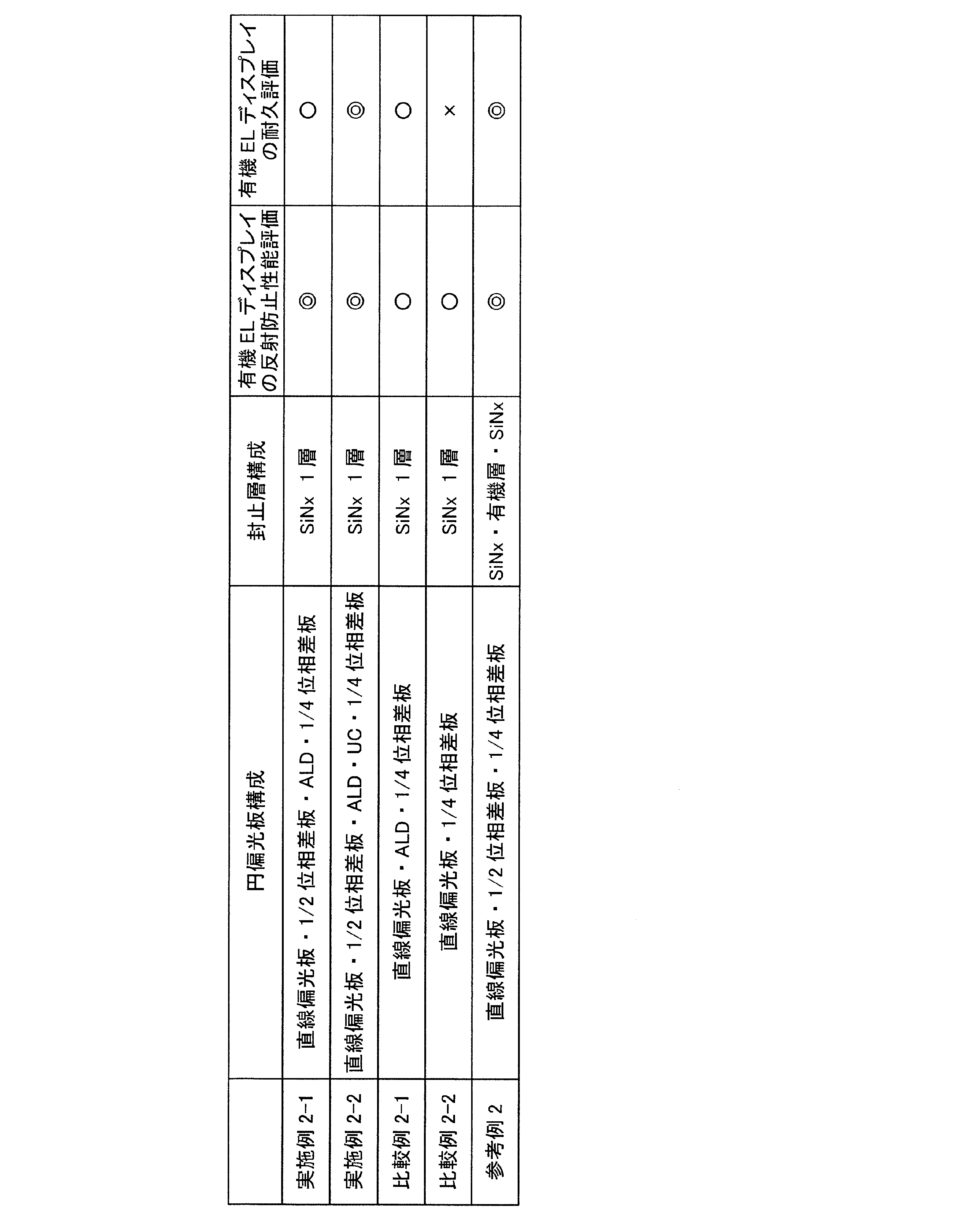
表2に示すように、実施例2-1、2-2に係る有機ELディスプレイは、参考例2に係る有機ELディスプレイと比較して、同等又は同等に近い耐久性を有することを確認した。また、比較例2-2に係る有機ELディスプレイは、参考例2に係る有機ELディスプレイと比較して、耐久性が大きく劣ることを確認した。また、実施例2-1、2-2に係る有機ELディスプレイは、参考例2に係る有機ELディスプレイと比較して、同等の反射防止性能を有することを確認した。
(有機ELディスプレイにおける背景の映りこみ等について)
有機ELディスプレイでは、外光の反射や背景の映りこみ等が生ずることがある。これらを防止するために、直線偏光板と1/4波長板を積層した円偏光板が用いられることがある。有機ELディスプレイの薄型化へのアプローチとして、例えば特開2002-156524号公報では、1/4波長板に無機膜を形成することで、EL素子の積層数を低減している。
しかし、位相差板を構成する高分子フィルムには屈折率の波長依存性がある。そのため、波長領域の広い光に対しては、一種類の波長板では、十分な反射防止性能が得られない場合がある。
しかしながら、上述した第4、第5、第6の各実施形態に係るガスバリア性位相差フィルム及びこれを備えた有機ELディスプレイであれば、高いガスバリア性と高い反射防止性能を有し、更なる薄膜化を可能とし得る。
有機ELディスプレイでは、外光の反射や背景の映りこみ等が生ずることがある。これらを防止するために、直線偏光板と1/4波長板を積層した円偏光板が用いられることがある。有機ELディスプレイの薄型化へのアプローチとして、例えば特開2002-156524号公報では、1/4波長板に無機膜を形成することで、EL素子の積層数を低減している。
しかし、位相差板を構成する高分子フィルムには屈折率の波長依存性がある。そのため、波長領域の広い光に対しては、一種類の波長板では、十分な反射防止性能が得られない場合がある。
しかしながら、上述した第4、第5、第6の各実施形態に係るガスバリア性位相差フィルム及びこれを備えた有機ELディスプレイであれば、高いガスバリア性と高い反射防止性能を有し、更なる薄膜化を可能とし得る。
10 ガスバリア性位相差フィルム
11 位相差板(第1の位相差板)
11´ ガスバリア性位相差板
11´´ ガスバリア性位相差板
12 原子層堆積膜
13 粘着層
14 偏光板
15 アンダーコート層
16 オーバーコート層
17 剥離フィルム
18 ハードコート層
19 ハードコート層
20 ガスバリア性位相差フィルム
21 粘着層
30 有機EL素子
31 支持基板
32 素子本体
33、330 封止層
41 粘着層
42 カバーガラス
50 有機ELディスプレイ
60 ガスバリア性位相差フィルム
61 位相差板(第2の位相差板)
61´ ガスバリア性位相差板
62 粘着層
70 ガスバリア性位相差フィルム
80 有機ELディスプレイ
331、333 無機層
332 有機層
11 位相差板(第1の位相差板)
11´ ガスバリア性位相差板
11´´ ガスバリア性位相差板
12 原子層堆積膜
13 粘着層
14 偏光板
15 アンダーコート層
16 オーバーコート層
17 剥離フィルム
18 ハードコート層
19 ハードコート層
20 ガスバリア性位相差フィルム
21 粘着層
30 有機EL素子
31 支持基板
32 素子本体
33、330 封止層
41 粘着層
42 カバーガラス
50 有機ELディスプレイ
60 ガスバリア性位相差フィルム
61 位相差板(第2の位相差板)
61´ ガスバリア性位相差板
62 粘着層
70 ガスバリア性位相差フィルム
80 有機ELディスプレイ
331、333 無機層
332 有機層
Claims (22)
- 位相差板と、
前記位相差板の一方の面側に形成された原子層堆積膜と、
を備えることを特徴とするガスバリア性位相差フィルム。 - 前記位相差板と前記原子層堆積膜との層間に形成された、無機材料からなるアンダーコート層、をさらに備えることを特徴とする請求項1に記載のガスバリア性位相差フィルム。
- 前記原子層堆積膜の前記位相差板と向かい合う面とは反対の面側に形成されたオーバーコート層、をさらに備えることを特徴とする請求項1又は2に記載のガスバリア性位相差フィルム。
- 請求項1~3の何れか一項に記載のガスバリア性位相差フィルムのいずれか一方の面側に設けられた偏光板、をさらに備えることを特徴とするガスバリア性位相差フィルム。
- 前記原子層堆積膜の前記位相差板と向かい合う面とは反対の面側であって、最も外側に剥離可能に形成された剥離フィルム、をさらに備えることを特徴とする請求項1~3の何れか一項に記載のガスバリア性位相差フィルム。
- 前記位相差板の前記剥離フィルム側の面とは反対の面側に設けられた偏光板、をさらに備えることを特徴とする請求項5に記載のガスバリア性位相差フィルム。
- 前記原子層堆積膜の前記位相差板と向かい合う面とは反対の面側に形成された粘着層、をさらに備えることを特徴とする請求項1又は2に記載のガスバリア性位相差フィルム。
- 前記原子層堆積膜と、前記粘着層との層間に形成されたオーバーコート層、をさらに備えることを特徴とする請求項7に記載のガスバリア性位相差フィルム。
- 前記位相差板の前記原子層堆積膜と向かい合う面とは反対の面側に粘着層を介して積層された偏光板、をさらに有することを特徴とする請求項7又は8に記載のガスバリア性位相差フィルム。
- 前記位相差板の前記原子層堆積膜と向かい合う面とは反対の面側に形成された粘着層、をさらに備えることを特徴とする請求項1又は2に記載のガスバリア性位相差フィルム。
- 前記原子層堆積膜の前記位相差板と向かい合う面とは反対の面側に粘着層を介して積層された偏光板、をさらに有することを特徴とする請求項10に記載のガスバリア性位相差フィルム。
- 前記粘着層の前記原子層堆積膜と向かい合う面とは反対の面側に剥離可能に形成された剥離フィルム、をさらに備えることを特徴とする請求項7~11の何れか一項に記載のガスバリア性位相差フィルム。
- 前記位相差板の前記一方の面とは反対の面である他方の面側に形成された原子層堆積膜、をさらに備えることを特徴とする請求項1~12の何れか一項に記載のガスバリア性位相差フィルム。
- 第1の位相差板と、
前記第1の位相差板の一方の面側に形成された原子層堆積膜と、
前記原子層堆積膜の前記第1の位相差板と向かい合う面とは反対の面側に形成された粘着層と、
前記粘着層の前記原子層堆積膜と向かい合う面とは反対の面側に形成された第2の位相差板と、
を備えることを特徴とするガスバリア性位相差フィルム。 - 前記第2の位相差板の前記粘着層と向かい合う面とは反対の面側に形成された原子層堆積膜、をさらに備えることを特徴とする請求項14に記載のガスバリア性位相差フィルム。
- 前記第2の位相差板の前記粘着層と向かい合う面とは反対の面側に、前記原子層堆積膜を介して形成されたオーバーコート層、をさらに備えることを特徴とする請求項15に記載のガスバリア性位相差フィルム。
- 前記第1の位相差板と前記第2の位相差板とは、相互の位相差が異なっていることを特徴とする請求項14~16の何れか一項に記載のガスバリア性位相差フィルム。
- 前記第1の位相差板と、前記第1の位相差板に最も近い前記原子層堆積膜との層間に形成された、無機材料からなるアンダーコート層、をさらに備えることを特徴とする請求項14~17の何れか一項に記載のガスバリア性位相差フィルム。
- いずれかの位相差板と原子層堆積膜とが積層したものをガスバリア性位相差板と呼ぶとき、
いずれかの位相差板もしくはガスバリア性位相差板の最も外側に、粘着層を介して設けられた直線偏光板、をさらに備えることを特徴とする請求項14~18の何れか一項に記載のガスバリア性位相差フィルム。 - 前記第1の位相差板の前記一方の面とは反対の面である他方の面側に形成された原子層堆積膜、をさらに備えることを特徴とする請求項14~19の何れか一項に記載のガスバリア性位相差フィルム。
- 請求項1~20の何れか一項に記載のガスバリア性位相差フィルムと、
素子本体、前記素子本体を封止する封止層および前記素子本体を支持する支持基板を備えた有機EL素子とが、
前記ガスバリア性位相差フィルムに粘着層を介して接合されることを特徴とする有機ELディスプレイ。 - 前記封止層は、無機膜からなることを特徴とする請求項21に記載の有機ELディスプレイ。
Applications Claiming Priority (6)
| Application Number | Priority Date | Filing Date | Title |
|---|---|---|---|
| JP2016098087 | 2016-05-16 | ||
| JP2016-098086 | 2016-05-16 | ||
| JP2016-098087 | 2016-05-16 | ||
| JP2016098086 | 2016-05-16 | ||
| JP2016-204345 | 2016-10-18 | ||
| JP2016204345 | 2016-10-18 |
Publications (1)
| Publication Number | Publication Date |
|---|---|
| WO2017199885A1 true WO2017199885A1 (ja) | 2017-11-23 |
Family
ID=60326247
Family Applications (1)
| Application Number | Title | Priority Date | Filing Date |
|---|---|---|---|
| PCT/JP2017/018082 Ceased WO2017199885A1 (ja) | 2016-05-16 | 2017-05-12 | ガスバリア性位相差フィルム及び有機elディスプレイ |
Country Status (1)
| Country | Link |
|---|---|
| WO (1) | WO2017199885A1 (ja) |
Cited By (1)
| Publication number | Priority date | Publication date | Assignee | Title |
|---|---|---|---|---|
| WO2018074524A1 (ja) * | 2016-10-19 | 2018-04-26 | 凸版印刷株式会社 | ガスバリア性光学フィルム及び有機elディスプレイ |
Citations (5)
| Publication number | Priority date | Publication date | Assignee | Title |
|---|---|---|---|---|
| JP2009123511A (ja) * | 2007-11-14 | 2009-06-04 | Canon Inc | 発光装置 |
| WO2013161894A1 (ja) * | 2012-04-25 | 2013-10-31 | コニカミノルタ株式会社 | ガスバリア性フィルム、電子デバイス用基板および電子デバイス |
| JP2015088457A (ja) * | 2013-10-29 | 2015-05-07 | エルジー ディスプレイ カンパニー リミテッド | 有機電界発光表示装置及びその製造方法 |
| JP2015103522A (ja) * | 2013-11-26 | 2015-06-04 | エルジー ディスプレイ カンパニー リミテッド | 有機発光表示装置及びその製造方法 |
| JP2015103525A (ja) * | 2013-11-27 | 2015-06-04 | エルジー ディスプレイ カンパニー リミテッド | 有機発光表示装置及びその製造方法 |
-
2017
- 2017-05-12 WO PCT/JP2017/018082 patent/WO2017199885A1/ja not_active Ceased
Patent Citations (5)
| Publication number | Priority date | Publication date | Assignee | Title |
|---|---|---|---|---|
| JP2009123511A (ja) * | 2007-11-14 | 2009-06-04 | Canon Inc | 発光装置 |
| WO2013161894A1 (ja) * | 2012-04-25 | 2013-10-31 | コニカミノルタ株式会社 | ガスバリア性フィルム、電子デバイス用基板および電子デバイス |
| JP2015088457A (ja) * | 2013-10-29 | 2015-05-07 | エルジー ディスプレイ カンパニー リミテッド | 有機電界発光表示装置及びその製造方法 |
| JP2015103522A (ja) * | 2013-11-26 | 2015-06-04 | エルジー ディスプレイ カンパニー リミテッド | 有機発光表示装置及びその製造方法 |
| JP2015103525A (ja) * | 2013-11-27 | 2015-06-04 | エルジー ディスプレイ カンパニー リミテッド | 有機発光表示装置及びその製造方法 |
Cited By (1)
| Publication number | Priority date | Publication date | Assignee | Title |
|---|---|---|---|---|
| WO2018074524A1 (ja) * | 2016-10-19 | 2018-04-26 | 凸版印刷株式会社 | ガスバリア性光学フィルム及び有機elディスプレイ |
Similar Documents
| Publication | Publication Date | Title |
|---|---|---|
| CN103682154B (zh) | 一种有机电致发光显示器件及显示装置 | |
| US10192939B2 (en) | Display device and fabrication method thereof | |
| KR102311060B1 (ko) | 플라스틱 기판 및 이를 포함하는 표시장치 | |
| JP5871408B1 (ja) | 偏光板および光学積層体 | |
| CN104854646A (zh) | 显示装置 | |
| WO2019088192A1 (ja) | 反射防止層付偏光板およびその製造方法 | |
| KR102280836B1 (ko) | 편광판 | |
| JP7391338B2 (ja) | 偏光板の製造方法 | |
| TW201504051A (zh) | 用於顯示裝置之視窗及包含其之顯示裝置 | |
| KR102000051B1 (ko) | 플렉시블 유기 발광 표시 장치 및 그의 제조 방법 | |
| JP2018099811A (ja) | ガスバリア性光学フィルム及び有機elディスプレイ | |
| JP2015208960A (ja) | ガスバリア性積層フィルム及び有機elデバイス | |
| WO2017026078A1 (ja) | 偏光板、画像表示装置、及び偏光板の製造方法 | |
| WO2017199885A1 (ja) | ガスバリア性位相差フィルム及び有機elディスプレイ | |
| WO2018074524A1 (ja) | ガスバリア性光学フィルム及び有機elディスプレイ | |
| KR102289805B1 (ko) | 가식 부착 적층체, 광학 적층체 및 플렉서블 화상 표시 장치 | |
| JP7628010B2 (ja) | 反射防止層付き偏光板および画像表示装置 | |
| JPWO2018181181A1 (ja) | 透明導電性ガスバリア積層体及びこれを備えたデバイス | |
| JP5162805B2 (ja) | エレクトロルミネッセンスディスプレイ | |
| JP2023007352A (ja) | 積層体及びその製造方法、並びに、偏光フィルムの製造方法 | |
| WO2017134754A1 (ja) | 偏光板および光学積層体 | |
| WO2018056401A1 (ja) | ガスバリア性光学フィルム及び有機elディスプレイ | |
| KR102325624B1 (ko) | Oled용 편광판 및 이를 포함하는 화상표시장치 | |
| CN115588372B (zh) | 一种显示面板 | |
| WO2017134753A1 (ja) | 偏光板 |
Legal Events
| Date | Code | Title | Description |
|---|---|---|---|
| NENP | Non-entry into the national phase |
Ref country code: DE |
|
| 121 | Ep: the epo has been informed by wipo that ep was designated in this application |
Ref document number: 17799309 Country of ref document: EP Kind code of ref document: A1 |
|
| 122 | Ep: pct application non-entry in european phase |
Ref document number: 17799309 Country of ref document: EP Kind code of ref document: A1 |
|
| NENP | Non-entry into the national phase |
Ref country code: JP |