WO2017199616A1 - スイッチ部品、高周波モジュール及び通信装置 - Google Patents
スイッチ部品、高周波モジュール及び通信装置 Download PDFInfo
- Publication number
- WO2017199616A1 WO2017199616A1 PCT/JP2017/014159 JP2017014159W WO2017199616A1 WO 2017199616 A1 WO2017199616 A1 WO 2017199616A1 JP 2017014159 W JP2017014159 W JP 2017014159W WO 2017199616 A1 WO2017199616 A1 WO 2017199616A1
- Authority
- WO
- WIPO (PCT)
- Prior art keywords
- inductor
- selection
- switching circuit
- terminal
- switch component
- Prior art date
- Legal status (The legal status is an assumption and is not a legal conclusion. Google has not performed a legal analysis and makes no representation as to the accuracy of the status listed.)
- Ceased
Links
Images






Classifications
-
- H—ELECTRICITY
- H03—ELECTRONIC CIRCUITRY
- H03H—IMPEDANCE NETWORKS, e.g. RESONANT CIRCUITS; RESONATORS
- H03H7/00—Multiple-port networks comprising only passive electrical elements as network components
- H03H7/38—Impedance-matching networks
-
- H—ELECTRICITY
- H04—ELECTRIC COMMUNICATION TECHNIQUE
- H04B—TRANSMISSION
- H04B1/00—Details of transmission systems, not covered by a single one of groups H04B3/00 - H04B13/00; Details of transmission systems not characterised by the medium used for transmission
- H04B1/02—Transmitters
- H04B1/04—Circuits
- H04B1/0458—Arrangements for matching and coupling between power amplifier and antenna or between amplifying stages
-
- H—ELECTRICITY
- H03—ELECTRONIC CIRCUITRY
- H03H—IMPEDANCE NETWORKS, e.g. RESONANT CIRCUITS; RESONATORS
- H03H7/00—Multiple-port networks comprising only passive electrical elements as network components
- H03H7/01—Frequency selective two-port networks
- H03H7/0153—Electrical filters; Controlling thereof
- H03H7/0161—Bandpass filters
-
- H—ELECTRICITY
- H03—ELECTRONIC CIRCUITRY
- H03H—IMPEDANCE NETWORKS, e.g. RESONANT CIRCUITS; RESONATORS
- H03H7/00—Multiple-port networks comprising only passive electrical elements as network components
- H03H7/01—Frequency selective two-port networks
- H03H7/17—Structural details of sub-circuits of frequency selective networks
- H03H7/1741—Comprising typical LC combinations, irrespective of presence and location of additional resistors
- H03H7/175—Series LC in series path
-
- H—ELECTRICITY
- H03—ELECTRONIC CIRCUITRY
- H03K—PULSE TECHNIQUE
- H03K17/00—Electronic switching or gating, i.e. not by contact-making and –breaking
- H03K17/51—Electronic switching or gating, i.e. not by contact-making and –breaking characterised by the components used
- H03K17/56—Electronic switching or gating, i.e. not by contact-making and –breaking characterised by the components used by the use, as active elements, of semiconductor devices
- H03K17/687—Electronic switching or gating, i.e. not by contact-making and –breaking characterised by the components used by the use, as active elements, of semiconductor devices the devices being field-effect transistors
-
- H—ELECTRICITY
- H03—ELECTRONIC CIRCUITRY
- H03K—PULSE TECHNIQUE
- H03K17/00—Electronic switching or gating, i.e. not by contact-making and –breaking
- H03K17/51—Electronic switching or gating, i.e. not by contact-making and –breaking characterised by the components used
- H03K17/74—Electronic switching or gating, i.e. not by contact-making and –breaking characterised by the components used by the use, as active elements, of diodes
-
- H—ELECTRICITY
- H04—ELECTRIC COMMUNICATION TECHNIQUE
- H04B—TRANSMISSION
- H04B1/00—Details of transmission systems, not covered by a single one of groups H04B3/00 - H04B13/00; Details of transmission systems not characterised by the medium used for transmission
- H04B1/06—Receivers
- H04B1/16—Circuits
- H04B1/18—Input circuits, e.g. for coupling to an antenna or a transmission line
-
- H—ELECTRICITY
- H04—ELECTRIC COMMUNICATION TECHNIQUE
- H04B—TRANSMISSION
- H04B1/00—Details of transmission systems, not covered by a single one of groups H04B3/00 - H04B13/00; Details of transmission systems not characterised by the medium used for transmission
- H04B1/38—Transceivers, i.e. devices in which transmitter and receiver form a structural unit and in which at least one part is used for functions of transmitting and receiving
- H04B1/40—Circuits
- H04B1/403—Circuits using the same oscillator for generating both the transmitter frequency and the receiver local oscillator frequency
-
- H—ELECTRICITY
- H03—ELECTRONIC CIRCUITRY
- H03H—IMPEDANCE NETWORKS, e.g. RESONANT CIRCUITS; RESONATORS
- H03H7/00—Multiple-port networks comprising only passive electrical elements as network components
- H03H7/01—Frequency selective two-port networks
- H03H2007/013—Notch or bandstop filters
-
- H—ELECTRICITY
- H03—ELECTRONIC CIRCUITRY
- H03H—IMPEDANCE NETWORKS, e.g. RESONANT CIRCUITS; RESONATORS
- H03H7/00—Multiple-port networks comprising only passive electrical elements as network components
- H03H7/38—Impedance-matching networks
- H03H2007/386—Multiple band impedance matching
Definitions
- the present invention relates to a switch component, a high frequency module, and a communication device.
- Recent mobile terminals are required to support a plurality of frequency bands and a plurality of wireless systems, so-called multiband and multimode, with one terminal.
- a high-frequency module provided with a high-frequency switch in which a frequency band (band) for communication is appropriately selected has been proposed.
- Patent Document 1 describes a technique related to such a high-frequency module.
- the present invention has been made to solve the above-described problems, and an object thereof is to provide a switch component, a high-frequency module, and a communication device that can reduce the size of the high-frequency module.
- a switch component includes a common terminal, at least two selection terminals, and switching for selectively connecting the common terminal and each of the at least two selection terminals.
- a circuit and an inductor are provided, and one end of the inductor is connected to one selection terminal of the at least two selection terminals, and the switching circuit and the inductor are integrally provided.
- an inductor mounted in a space different from a space where a switch component in a high frequency module realized by an LTCC (Low Temperature Co-fired Ceramics) substrate is mounted is provided integrally with the switching circuit.
- the fact that the inductor is provided integrally with the switching circuit means that the inductor is built in the switching circuit (for example, a semiconductor substrate) or placed on the switching circuit and integrated with a resin mold or the like.
- an impedance matching circuit, a resonance circuit, or a filter constituted by the inductor is an element (for example, an antenna element) connected to the common terminal side when the common terminal and a selection terminal to which one end of the inductor is connected are connected.
- a signal propagating through a signal path connecting the element connected to the selection terminal side for example, a filter.
- a coupler constituted by the inductor makes it possible to measure the intensity of the signal propagating in the signal path.
- the inductor useful for the high-frequency module is provided integrally with the switching circuit, a space for mounting the inductor in the high-frequency module is reduced, and thus the high-frequency module can be reduced in size.
- other components can be mounted on the high-frequency module by the amount of mounting space reduced by providing the inductor integrally with the switching circuit, so that heat dissipation generated by adding a filter or heat generated by the filter can be improved.
- the inductor may be incorporated in the switching circuit.
- the high-frequency module can be downsized in the height direction as compared with the case where the inductor is mounted on the switching circuit.
- the inductor since the inductor is built in the switching circuit, the inductor can be protected.
- the other end of the inductor may be connected to a selection terminal different from the one selection terminal of the at least two selection terminals.
- the signal propagated through the signal path
- the impact given can be different.
- the common terminal is connected to the selection terminal to which one end of the inductor is connected, the signal is affected by the circuit configured by the inductor, and the common terminal is selected to be connected to the other end of the inductor.
- the signal can be prevented from being affected by the circuit constituted by the inductor.
- the other end of the inductor may be grounded.
- the circuit configured by the inductor functions as an impedance matching circuit, impedance matching between the switch component and the element connected to the selection terminal is made, and loss (return loss) generated in the signal propagating in the signal path is reduced. Can be suppressed.
- a capacitor may be connected in parallel to the inductor.
- the circuit configured by the inductor functions as a parallel resonant circuit, and noise such as harmonic components in a signal propagating through the signal path can be suppressed.
- the attenuation characteristic of the filter can be improved as an element connected to the selection terminal side.
- a circuit constituted by the inductor functions as a bandpass filter, and suppresses noise such as harmonic components and allows a signal having a desired frequency characteristic to pass. be able to.
- one end of a capacitor may be connected to the other end of the inductor.
- the circuit constituted by the inductor functions as a series resonance circuit, and functions as a band-pass filter that can suppress a noise such as a harmonic component and pass a signal having a desired frequency characteristic. Further, for example, noise such as harmonic components generated from the switch component superimposed on the signal can be suppressed.
- the other end of the capacitor may be grounded.
- the circuit constituted by the inductor functions as a band elimination filter, and noise such as harmonic components can be suppressed.
- the inductor may be coupled to a signal path between the common terminal connected by the switching circuit and one of the at least two selection terminals.
- a high-frequency module includes the above switch component and a filter connected to at least one selection terminal of the at least two selection terminals.
- the inductor is provided integrally with the switching circuit, the space for mounting the inductor in the high-frequency module is reduced, so that the high-frequency module can be reduced in size.
- a communication device includes the above-described high-frequency module and a control unit that controls the switching circuit.
- the inductor is provided integrally with the switching circuit, the space for mounting the inductor in the high-frequency module is reduced, so that the high-frequency module can be reduced in size.
- the high frequency module can be reduced in size.
- FIG. 1A is a configuration diagram illustrating an example of a switch component according to Embodiment 1.
- FIG. 1B is a schematic external view illustrating an example of a switch component according to Embodiment 1.
- FIG. 1C is a schematic cross-sectional view of the switching circuit along the IC-IC line shown in FIG. 1B.
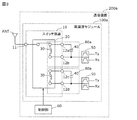
- FIG. 2 is a configuration diagram illustrating an example of the communication apparatus according to the first embodiment.
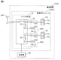
- FIG. 3 is a configuration diagram illustrating an example of a communication apparatus according to the second embodiment.
- FIG. 4 is a configuration diagram illustrating an example of a communication apparatus according to the third embodiment.
- FIG. 5 is a configuration diagram illustrating an example of a communication apparatus according to the fourth embodiment.
- FIG. 1A is a configuration diagram illustrating an example of a switch component according to Embodiment 1.
- FIG. 1B is a schematic external view illustrating an example of a switch component according to Embodiment 1.
- FIG. 1C is a schematic cross-sectional
- FIG. 6 is a configuration diagram illustrating an example of a communication apparatus according to the fifth embodiment.
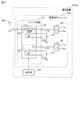
- FIG. 7 is a configuration diagram illustrating an example of a communication apparatus according to the sixth embodiment.
- FIG. 8A is a configuration diagram illustrating an example of a switch component according to another embodiment.
- FIG. 8B is a schematic external view illustrating an example of a switch component according to another embodiment.
- FIG. 1A is a configuration diagram illustrating an example of the switch component 10 according to the first embodiment.
- the switch component 10 includes a common terminal 11, selection terminals 12a to 12d, and a switching circuit 20. Note that the switch component 10 only needs to include at least two selection terminals. For example, the switch component 10 may include only two selection terminals, or may include three or five or more selection terminals.
- the switching circuit 20 is a circuit that selectively connects the common terminal 11 and each of at least two selection terminals (here, selection terminals 12a to 12d). For example, a PIN diode or a MESFET (METAL Semiconductor Field Effect Transistor) or the like. This is realized by a switch using a semiconductor.
- the switching circuit 20 selectively connects the common terminal 11 and each of at least two selection terminals by receiving, for example, a control signal from the outside.
- an antenna element is connected to the common terminal 11, and filters (for example, duplexers) having different pass frequency bands are connected to the selection terminals 12a to 12d, for example.
- the switching circuit 20 selectively selects a frequency band for communication by selectively connecting the common terminal 11 and any one of the selection terminals 12a to 12d.
- the switching circuit 20 can selectively connect the common terminal 11 and any one of the selection terminals 12a to 12d.
- FIG. 1A shows a state where the common terminal 11 and the selection terminal 12a are connected as an example. 2 to 8A described below, the state where the common terminal 11 and the selection terminal 12a are connected is shown, but all are examples, and the common terminal 11 and another selection terminal can be connected.
- connection form of the elements connected to the selection terminals 12a and 12b and the connection form of the elements connected to the selection terminals 12c and 12d are the same. Therefore, the description of the connection form of the elements connected to the selection terminals 12c and 12d is omitted.
- the characteristics of the elements around the selection terminals 12a and 12b may be different from the characteristics of the elements around the selection terminals 12c and 12d.
- the selection terminals 12c and 12d may be connected to a filter having a different pass frequency band than the selection terminals 12a and 12b, an inductor having a different inductance, or a capacitor having a different capacitance.
- the switch component 10 includes an inductor 30.
- the inductor 30 configures, for example, an impedance matching circuit, a resonance circuit, a filter, or a coupler. Details of the circuit formed by the inductor 30 will be described later.
- One end of the inductor 30 is connected to one selection terminal 12a of at least two selection terminals (selection terminals 12a and 12b).
- the other end of the inductor 30 is connected to a selection terminal 12b different from one selection terminal 12a of at least two selection terminals.
- the switching circuit 20 and the inductor 30 are provided integrally.
- the inductor 30 is built in the switching circuit 20.
- the switch component 10 when the inductor 30 is built in the switching circuit 20 will be described with reference to FIGS. 1B and 1C.
- FIG. 1B is a schematic external view illustrating an example of the switch component 10 according to the first exemplary embodiment.
- FIG. 1C is a schematic cross-sectional view of the switching circuit 20 along the IC-IC line shown in FIG. 1B. 1B and 1C, the lead conductor of the inductor 30, the common terminal 11, and the selection terminals 12a to 12d are not shown.
- the switching circuit 20 is, for example, a semiconductor substrate on which a plurality of base material layers 21 are stacked.
- the switching circuit 20 is realized as a switch using a semiconductor such as a PIN diode or MESFET.
- the base material layer 21 on which a pattern of a metal or alloy mainly composed of silver is printed or etched or the like is disposed around the center in the stacking direction of the stacked base material layers 21.
- the switching circuit 20 having the inductor 30 built therein is realized.
- the shape of the inductor 30 is not limited to the shape in which a pattern is printed on one base material layer 21 as shown in FIGS. 1B and 1C.
- the shape of the inductor 30 may be a spiral shape in which patterns printed on the plurality of base material layers 21 are connected by interlayer conductors (via conductors).
- the inductor 30 useful for the high-frequency module is provided integrally with the switching circuit 20 (for example, the inductor 30 is incorporated in the switching circuit 20), so that a space for mounting the inductor 30 in the high-frequency module is provided. Therefore, the high-frequency module can be reduced in size.
- FIG. 2 is a configuration diagram illustrating an example of the communication apparatus 200 according to the first embodiment.
- FIG. 2 also shows the antenna element ANT.
- the communication device 200 is a device provided in a multimode / multiband portable terminal, and receives and transmits signals via an antenna element ANT.
- the communication device 200 includes a high-frequency module 100 and a control unit 60.
- the high-frequency module 100 includes a switch component 10 and a filter 50.
- the high frequency module 100 is realized by, for example, an LTCC substrate on which the switch component 10 and the filter 50 are mounted.
- the high frequency module 100 is disposed, for example, in a front end portion of a mobile terminal.
- the filter 50 is a filter element having pass characteristics for transmitting a high-frequency signal in a predetermined frequency band.
- the filter 50 is, for example, a duplexer, and in communication using a frequency division duplex (FDD) system, the transmission path (Tx) and the reception path (Rx) are shared while sharing one antenna element ANT. Switch.
- FDD frequency division duplex
- the filter 50 separates (demultiplexes) the transmission signal and the reception signal.
- the filter 50 connected to the selection terminal 12a and the filter 50 connected to the selection terminal 12c shown in FIG. 2 pass high-frequency signals in different frequency bands.
- the filter 50 connected to the selection terminal 12a passes the signal in the first pass band
- the filter 50 connected to the selection terminal 12c passes the signal in the second pass band lower than the first pass band, for example. Let it pass.
- the controller 60 is, for example, an RFIC (Radio Frequency Integrated Circuit) that processes a high-frequency signal, and selectively connects the common terminal 11 and each of at least two selection terminals by controlling the switching circuit 20.
- the control unit 60 is realized by, for example, a processor that executes a control program stored in a storage unit (not shown) included in the communication device 200, but may be realized by a microcomputer or a dedicated circuit.
- the common terminal 11 and the selection terminals 12a to 12d are selectively connected in the switch component 10, so that a predetermined frequency band corresponding to the pass characteristic of the filter 50 connected to the selection terminal is obtained.
- a high-frequency signal is selectively passed.
- the frequency band of the signal to communicate becomes the pass frequency band of the upper filter 50 in FIG.
- the common terminal 11 and the selection terminal 12c are connected, the frequency band of the signal to be communicated is the pass frequency band of the lower filter 50 in FIG.
- the high-frequency module 100 is provided with a plurality of switchable signal paths for transmitting and receiving signals in a plurality of frequency bands so as to correspond to the multimode and the multiband.
- the other end of the inductor 30 is grounded (for example, the selection terminal 12b is grounded), so that the inductor 30 is used as a shunt inductor for impedance matching. Therefore, the impedance matching circuit 70 is configured by the inductor 30. Thereby, impedance matching is performed between the switch component 10 and the filter 50 connected to the selection terminal 12a, for example.
- the filter connected to the antenna element ANT and the selection terminal 12a. 50 the loss that occurs in the signal propagating through the signal path that connects the signal line 50 can be suppressed.
- the inductor 30 which comprises the impedance matching circuit 70 is provided integrally with the switching circuit 20, and the high frequency module 100 can be reduced in size.
- both ends of the inductor 30 may not be connected to the selection terminals.
- one end of the inductor 30 may be connected to the selection terminal 12a and the other end may not be connected to another selection terminal.
- the other end of the inductor 30 is connected to a terminal or the like that is not selectively switched by the switching circuit 20.
- the terminals indicated as selection terminals 12b and 12d in FIG. 2 may not be selection terminals. That is, the terminals indicated as the selection terminals 12 b and 12 d may not be terminals that can be connected to the common terminal 11.
- connection form of the peripheral elements and the like of each of the selection terminals shown in FIG. 2 is an example.
- the filter 50 may be connected to the selection terminal 12b and the selection terminal 12a may be grounded. In this case, when the common terminal 11 and the selection terminal 12b are connected, it is possible to suppress a loss generated in a signal propagating through a signal path connecting the antenna element ANT and the filter 50 connected to the selection terminal 12b. .
- FIG. 3 is a configuration diagram illustrating an example of the communication apparatus 200a according to the second embodiment.
- the communication device 200a is different from the communication device 200 according to the first embodiment in that the communication device 200a includes the high-frequency module 100a instead of the high-frequency module 100. Further, the connection form of the peripheral elements and the like of each of the selection terminals is different from that in the first embodiment. Since other configurations are the same as those in the first embodiment, description thereof is omitted.
- the high-frequency module 100a includes a capacitor 40 connected in parallel to the inductor 30, and the parallel resonance circuit 80a is configured by the inductor 30 and the capacitor 40, and functions as a band elimination filter.
- the filter 50 is connected to the selection terminal 12b, when the common terminal 11 and the selection terminal 12a are connected, a signal path that connects the antenna element ANT and the filter 50 connected to the selection terminal 12b is propagated. For example, noise such as harmonic components in the signal can be suppressed.
- the inductor 30 which comprises the parallel resonance circuit 80a is provided integrally with the switching circuit 20, and the high frequency module 100a can be reduced in size.
- each peripheral element etc. of the selection terminal shown in FIG. 3 is an example.
- the filter 50 may be connected to the selection terminal 12a.
- the common terminal 11 and the selection terminal 12b are connected, for example, a harmonic component or the like in a signal propagating through a signal path connecting the antenna element ANT and the filter 50 connected to the selection terminal 12a. Noise can be suppressed.
- FIG. 4 is a configuration diagram illustrating an example of the communication apparatus 200b according to the third embodiment.
- the communication device 200b is different from the communication device 200 according to the first embodiment in that the communication device 200b includes the high-frequency module 100b instead of the high-frequency module 100. Further, the connection form of the peripheral elements and the like of each of the selection terminals is different from that in the first embodiment. Since other configurations are the same as those in the first embodiment, description thereof is omitted.
- the high frequency module 100 b includes a capacitor 40 connected in parallel to the inductor 30.
- the other end of the inductor 30 is grounded (the selection terminal 12b is grounded), so that a circuit configured by the inductor 30 functions as a bandpass filter 80b.
- noise such as harmonic components in a signal propagating through the signal path connecting the antenna element ANT and the filter 50 connected to the selection terminal 12a is suppressed.
- a signal having a desired frequency characteristic can be passed.
- the inductor 30 which comprises the band pass filter 80b is provided integrally with the switching circuit 20, and the high frequency module 100b can be reduced in size.
- each peripheral element etc. of the selection terminal shown in FIG. 4 is an example.
- the filter 50 may be connected to the selection terminal 12b and the selection terminal 12a may be grounded.
- noise such as harmonic components in the signal propagating through the signal path connecting the antenna element ANT and the filter 50 connected to the selection terminal 12b. It is possible to pass a signal having a desired frequency characteristic with suppressed.
- FIG. 5 is a configuration diagram illustrating an example of the communication apparatus 200c according to the fourth embodiment.
- the communication device 200 c is different from the communication device 200 according to the first embodiment in that the communication device 200 c includes the high-frequency module 100 c instead of the high-frequency module 100. Further, the connection form of the peripheral elements and the like of each of the selection terminals is different from that in the first embodiment. Since other configurations are the same as those in the first embodiment, description thereof is omitted.
- the high-frequency module 100c includes a capacitor 40, and one end of the capacitor 40 is connected to the other end (selection terminal 12b) of the inductor 30, whereby the series resonance circuit 80c is configured by the inductor 30 and the capacitor 40, and a bandpass filter is formed. And function.
- a filter 50 is connected to the other end of the capacitor 40.
- connection form of the peripheral elements and the like of each of the selection terminals shown in FIG. 5 is an example.
- one end of the capacitor 40 may be connected to one end (selection terminal 12a) of the inductor 30, and the filter 50 may be connected to the other end of the capacitor 40.
- the common terminal 11 and the selection terminal 12b are connected, for example, in a signal propagating through a signal path connecting the antenna element ANT and the filter 50 connected to the selection terminal 12a via the capacitor 40, for example.
- a signal having a desired frequency characteristic in which noise such as harmonic components is suppressed can be passed.
- FIG. 6 is a configuration diagram illustrating an example of a communication device 200d according to the sixth embodiment.
- the communication device 200d is different from the communication device 200 according to the first embodiment in that the communication device 200d includes the high-frequency module 100d instead of the high-frequency module 100. Further, the connection form of the peripheral elements and the like of each of the selection terminals is different from that in the first embodiment. Since other configurations are the same as those in the first embodiment, description thereof is omitted.
- the high-frequency module 100d includes a capacitor 40, and one end of the capacitor 40 is connected to the other end (selection terminal 12b) of the inductor 30.
- a circuit constituted by the inductor 30 functions as a band elimination filter 80d.
- the inductor 30 which comprises the band elimination filter 80d is provided integrally with the switching circuit 20, and the high frequency module 100d can be reduced in size.
- connection form of the peripheral elements and the like of each of the selection terminals shown in FIG. 6 is an example.
- one end of the capacitor 40 may be connected to one end (selection terminal 12a) of the inductor 30, and the other end of the capacitor 40 may be grounded.
- the common terminal 11 and the selection terminal 12b are connected, noise such as harmonic components in a signal propagating through a signal path connecting the antenna element ANT and the filter 50 connected to the selection terminal 12b is suppressed. it can.
- FIG. 7 is a configuration diagram illustrating an example of the communication device 200e according to the sixth embodiment.
- the communication device 200e is different from the communication device 200 according to the first embodiment in that the communication device 200e includes the high-frequency module 100e instead of the high-frequency module 100.
- the inductor 30 is coupled to the signal path 13 between the common terminal 11 connected by the switching circuit 20 and one of the at least two selection terminals (for example, the selection terminal 12a).
- the inductor 30 is provided in the vicinity of the signal path 13 in the switching circuit 20.
- the circuit constituted by the inductor 30 functions as the coupler 90.
- the connection form of the peripheral elements and the like of each of the selection terminals is different from that in the first embodiment. Since other configurations are the same as those in the first embodiment, description thereof is omitted.
- one end of the inductor 30 is connected to the selection terminal 12b, for example.
- the other end of the inductor 30 is grounded, for example, via a resistor 14 (for example, 50 ⁇ ).
- the inductor 30 constituting the coupler 90 capable of measuring the intensity of such a signal is provided integrally with the switching circuit 20, whereby the high-frequency module 100e can be reduced in size.
- connection form of each peripheral element etc. of the selection terminal shown in FIG. 7 is an example.
- the inductor 30 may be coupled to a signal path between the common terminal 11 and the selection terminal 12b connected by the switching circuit 20. Then, one end of the inductor 30 may be connected to the selection terminal 12a, and the other end may be grounded through the resistor 14, for example. Thereby, the intensity of the signal propagating through the signal path can be measured by monitoring the voltage at the selection terminal 12a.
- the control unit 60 is provided in the communication device, but is not limited thereto.
- the switch component 10 may include the control unit 60. That is, the switch component 10 (switching circuit 20) may selectively connect the common terminal 11 and each of the at least two selection terminals by the control unit 60 provided therein without receiving a control signal from the outside. .
- the filter 50 is a duplexer, but is not limited thereto.
- the filter 50 may be a low-pass filter, a high-pass filter, a band elimination filter, or the like.
- the inductor 30 is built in the switching circuit 20.
- the present invention is not limited to this.
- the inductor 30 may not be incorporated in the switching circuit 20. This will be described with reference to FIGS. 8A and 8B.
- FIG. 8A is a configuration diagram showing an example of a switch component 10a according to another embodiment.
- FIG. 8B is a schematic external view showing an example of a switch component 10a according to another embodiment.
- the lead conductor of the inductor 30, the common terminal 11, and the selection terminals 12a to 12d are not shown.
- the inductor 30 may be placed on the switching circuit 20 (for example, a semiconductor substrate). Then, the switching circuit 20 and the inductor 30 are integrated by a resin mold or the like. The switching circuit 20 and the inductor 30 integrated in this way are used as the switch component 10a. That is, in the above-described embodiment, the switch component 10 is the switching circuit 20 itself including the inductor 30, but the switch component 10 a is formed by resin-molding the switching circuit 20 and the inductor 30 placed on the switching circuit 20. Etc. are integrated. 8A is not a diagram showing that the inductor 30 is provided separately from the switching circuit 20, and that the inductor 30 is not built in the switching circuit 20 but is mounted on the switching circuit 20. FIG. In FIG. 8B, the inductor 30 is shown as a chip inductor, but may be a pattern printed on the switching circuit 20.
- control unit 60 may be realized as an integrated circuit IC or LSI (Large Scale Integration).
- the method of circuit integration may be realized by a dedicated circuit or a general-purpose processor.
- An FPGA Field Programmable Gate Array
- reconfigurable processor that can reconfigure the connection and setting of circuit cells inside the LSI may be used.
- integrated circuit technology comes out to replace LSI's as a result of the advancement of semiconductor technology or a derivative other technology, it is naturally also possible to carry out function block integration using this technology.
- the present invention can be widely used in communication devices such as mobile phones as multi-band / multi-mode compatible switch parts, high-frequency modules or communication devices.
Landscapes
- Engineering & Computer Science (AREA)
- Computer Networks & Wireless Communication (AREA)
- Signal Processing (AREA)
- Transceivers (AREA)
- Filters And Equalizers (AREA)
Abstract
スイッチ部品(10)は、共通端子(11)と、少なくとも2つの選択端子(12a~12d)と、共通端子(11)と少なくとも2つの選択端子(12a~12d)のそれぞれとを選択的に接続する切替回路(20)と、インダクタ(30)と、を備え、少なくとも2つの選択端子(12a~12d)のうちの1つの選択端子(12a~12d)には、インダクタ(30)の一端が接続され、切替回路(20)とインダクタ(30)とは、一体に設けられる。
Description
本発明は、スイッチ部品、高周波モジュール及び通信装置に関する。
近年の携帯端末には、1つの端末で複数の周波数帯域及び複数の無線方式、いわゆるマルチバンド化及びマルチモード化に対応することが要求されている。これに対応すべく、通信する周波数帯域(バンド)が適宜選択される高周波スイッチが設けられた高周波モジュールが提案されている。特許文献1には、このような高周波モジュールに関する技術が記載されている。
ところで、近年の携帯電話のマルチバンド化及びマルチモード化に伴い、高周波モジュールのさらなる小型化が要求されている。しかしながら、特許文献1に記載されているような高周波モジュールでは、マルチバンド機能及びマルチモード機能を実現しつつ小型化することは難しい。
そこで、本発明は、上記課題を解決するためになされたものであって、高周波モジュールを小型化できるスイッチ部品、高周波モジュール及び通信装置を提供することを目的とする。
上記目的を達成するために、本発明の一態様に係るスイッチ部品は、共通端子と、少なくとも2つの選択端子と、前記共通端子と前記少なくとも2つの選択端子のそれぞれとを選択的に接続する切替回路と、インダクタと、を備え、前記少なくとも2つの選択端子のうちの1つの選択端子には、前記インダクタの一端が接続され、前記切替回路と前記インダクタとは、一体に設けられる。
これにより、例えばLTCC(Low Temperature Co-fired Ceramics)基板により実現される高周波モジュールにおけるスイッチ部品が実装されたスペースとは異なるスペースに実装されていたインダクタが切替回路と一体に設けられる。インダクタが切替回路と一体に設けられるとは、インダクタが、切替回路(例えば半導体基板)に内蔵されたり、切替回路上に載置されて樹脂モールド等で一体化されたりすることである。当該インダクタにより構成される例えばインピーダンス整合回路、共振回路又はフィルタは、共通端子とインダクタの一端が接続された選択端子とが接続されたときの、共通端子側に接続される素子(例えばアンテナ素子)と当該選択端子側に接続される素子(例えばフィルタ)とを接続する信号経路を伝搬する信号に影響を与える。また、当該インダクタにより構成される例えばカプラは、信号経路を伝搬する信号の強度を測定可能にする。このように、高周波モジュールにとって有用なインダクタが切替回路と一体に設けられることで高周波モジュールにおいて当該インダクタが実装されるスペースが削減されるため、高周波モジュールを小型化できる。また、例えば、インダクタが切替回路と一体に設けられることで削減された実装スペース分、高周波モジュールに他の部品を実装することができるため、フィルタの追加又はフィルタにより発生する熱の放熱性の改善等をすることができる。
また、前記インダクタは、前記切替回路に内蔵されてもよい。
これにより、インダクタが切替回路に内蔵されることで、例えばインダクタが切替回路上に載置されるときよりも、高周波モジュールを高さ方向において小型化できる。また、インダクタが切替回路に内蔵されているため、インダクタを保護することができる。
また、前記少なくとも2つの選択端子のうちの前記1つの選択端子とは異なる選択端子には、前記インダクタの他端が接続されてもよい。
これにより、例えば、共通端子がインダクタの一端が接続された選択端子に接続された場合と、当該インダクタの他端が接続された選択端子に接続された場合とで、信号経路を伝搬する信号に与えられる影響を異なるものにできる。例えば、共通端子がインダクタの一端が接続された選択端子に接続された場合には、当該信号に当該インダクタにより構成される回路の影響を与え、共通端子が当該インダクタの他端が接続された選択端子に接続された場合には、当該信号に当該インダクタにより構成される回路の影響を与えないようにすることができる。
また、前記インダクタの他端は接地されてもよい。
これにより、インダクタにより構成される回路がインピーダンス整合回路として機能し、スイッチ部品と選択端子側に接続される素子とのインピーダンス整合がなされ、信号経路を伝搬する信号に発生する損失(リターンロス)を抑制できる。
また、前記インダクタにはコンデンサが並列に接続されてもよい。
これにより、インダクタの他端が接地されない場合には、当該インダクタにより構成される回路が並列共振回路として機能し、信号経路を伝搬する信号におけるノイズ、例えば高調波成分等のノイズを抑制できるバンドエリミネーションフィルタとして機能する。例えば、選択端子側に接続される素子としてフィルタの減衰特性を向上させることができる。また、インダクタの他端が接地される場合には、当該インダクタにより構成される回路が、バンドパスフィルタとして機能し、高調波成分等のノイズを抑制して所望の周波数特性を有する信号を通過させることができる。
また、前記インダクタの他端にはコンデンサの一端が接続されてもよい。
これにより、インダクタにより構成される回路が直列共振回路として機能し、高調波成分等のノイズを抑制して所望の周波数特性を有する信号を通過させることができるバンドパスフィルタとして機能する。また、例えば、当該信号に重畳した、スイッチ部品から発生される高調波成分等のノイズを抑制できる。
また、前記コンデンサの他端は接地されてもよい。
これにより、インダクタにより構成される回路がバンドエリミネーションフィルタとして機能し、高調波成分等のノイズを抑制できる。
また、前記インダクタは、前記切替回路によって接続した前記共通端子と前記少なくとも2つの選択端子のうちの一の選択端子との間の信号経路に結合されてもよい。
これにより、インダクタにより構成される回路をカプラとして機能させることが可能ととなり、インダクタが結合された信号経路を伝搬する信号の強度を測定することができる。したがって、このような信号の強度を測定可能なカプラを構成するインダクタが切替回路と一体に設けられることで、高周波モジュールの小型化が可能となる。
また、本発明の一態様に係る高周波モジュールは、上記のスイッチ部品と、前記少なくとも2つの選択端子のうちの少なくとも一の選択端子に接続されるフィルタと、を備える。
これにより、インダクタが切替回路と一体に設けられることで高周波モジュールにおいて当該インダクタが実装されるスペースが削減されるため、高周波モジュールを小型化できる。
また、本発明の一態様に係る通信装置は、上記の高周波モジュールと、前記切替回路を制御する制御部と、を備える。
これにより、インダクタが切替回路と一体に設けられることで高周波モジュールにおいて当該インダクタが実装されるスペースが削減されるため、高周波モジュールを小型化できる。
本発明に係るスイッチ部品、高周波モジュール及び通信装置によれば、高周波モジュールを小型化できる。
以下、本発明の実施の形態について、実施の形態及びその図面を用いて詳細に説明する。なお、以下で説明する実施の形態は、いずれも包括的又は具体的な例を示すものである。以下の実施の形態で示される数値、形状、材料、構成要素、構成要素の配置及び接続形態などは、一例であり、本発明を限定する主旨ではない。以下の実施の形態における構成要素のうち、独立請求項に記載されていない構成要素については、任意の構成要素として説明される。また、図面に示される構成要素の大きさ又は大きさの比は、必ずしも厳密ではない。
(実施の形態1)
[1.1 スイッチ部品の構成]
まず、実施の形態1に係るスイッチ部品10の構成について図1Aから図1Cを用いて説明する。
[1.1 スイッチ部品の構成]
まず、実施の形態1に係るスイッチ部品10の構成について図1Aから図1Cを用いて説明する。
図1Aは、実施の形態1に係るスイッチ部品10の一例を示す構成図である。
スイッチ部品10は、共通端子11と選択端子12a~12dと切替回路20とを備える。なお、スイッチ部品10は、少なくとも2つの選択端子を備えていればよい。例えば、スイッチ部品10は、2つの選択端子のみを備えていてもよく、3つ又は5つ以上の選択端子を備えていてもよい。
切替回路20は、共通端子11と少なくとも2つの選択端子(ここでは、選択端子12a~12d)のそれぞれとを選択的に接続する回路であり、例えばPINダイオード又はMESFET(MEtal Semiconductor Field Effect Transistor)等の半導体を用いたスイッチにより実現される。切替回路20は、例えば外部からの制御信号を受けることで、共通端子11と少なくとも2つの選択端子のそれぞれとを選択的に接続する。
共通端子11には、例えばアンテナ素子が接続され、選択端子12a~12dには、例えば通過周波数帯域の異なるフィルタ(例えばデュプレクサ等)が接続される。切替回路20は、共通端子11と選択端子12a~12dのいずれかとを選択的に接続することで、通信する周波数帯域が適宜選択される。切替回路20は、共通端子11と選択端子12a~12dのいずれかとを選択的に接続し得るが、図1Aには、一例として共通端子11と選択端子12aとを接続した状態が示される。なお、以下で説明する図2から図8Aについても共通端子11と選択端子12aとが接続された状態が示されるが、全て一例であり、共通端子11と他の選択端子とが接続され得る。また、以下で説明する図2から図8Aについて、選択端子12a及び12bに接続される素子等の接続形態と選択端子12c及び12dに接続される素子等の接続形態とを同じものとして説明する。したがって、選択端子12c及び12dに接続される素子等の接続形態については説明を省略する。ただし、選択端子12a及び12bの周辺の素子の特性と選択端子12c及び12dの周辺の素子の特性とが異なっていてもよい。例えば、選択端子12c及び12dには、選択端子12a及び12bとは異なる通過周波数帯域のフィルタ、異なるインダクタンスのインダクタ又は異なる静電容量のコンデンサ等が接続されてもよい。
スイッチ部品10はインダクタ30を備える。インダクタ30は、例えば、インピーダンス整合回路、共振回路、フィルタ又はカプラ等を構成する。インダクタ30が構成する回路の詳細については後述する。
少なくとも2つの選択端子(選択端子12a及び12b)のうちの1つの選択端子12aには、インダクタ30の一端が接続される。また、少なくとも2つの選択端子のうちの1つの選択端子12aとは異なる選択端子12bには、インダクタ30の他端が接続される。このとき、切替回路20とインダクタ30とは一体に設けられる。具体的には、インダクタ30は、切替回路20に内蔵される。ここで、インダクタ30が切替回路20に内蔵されたときのスイッチ部品10について図1B及び図1Cを用いて説明する。
図1Bは、実施の形態1に係るスイッチ部品10の一例を示す外観模式図である。
図1Cは、図1Bに示されるIC-IC線における切替回路20の断面模式図である。なお、図1B及び図1Cでは、インダクタ30の引き出し導体、並びに、共通端子11及び選択端子12a~12dの図示を省略している。
切替回路20は、例えば、複数の基材層21が積層された半導体基板である。切替回路20は、例えばPINダイオード又はMESFET等の半導体を用いたスイッチとして実現されている。また、例えば銀を主成分とする金属又は合金のパターンが印刷又はエッチング等された基材層21が、図1Cに示されるように、積層された複数の基材層21における積層方向の中央あたりに設けられることで、インダクタ30が内蔵された切替回路20が実現されている。なお、インダクタ30の形状は図1B及び図1Cに示されるように、1つの基材層21上にパターンが印刷等された形状に限らない。例えば、インダクタ30の形状は、複数の基材層21上に印刷等されたパターンが層間導体(ビア導体)によって接続されたらせん形状等であってもよい。
このように、高周波モジュールにとって有用なインダクタ30が切替回路20と一体に設けられることで(例えば、インダクタ30が切替回路20に内蔵されることで)、高周波モジュールにおいてインダクタ30が実装されるスペースが削減されるため、高周波モジュールを小型化できる。
[1.2 通信装置の構成]
次に、通信装置200の構成について図2を用いて説明する。
次に、通信装置200の構成について図2を用いて説明する。
図2は、実施の形態1に係る通信装置200の一例を示す構成図である。なお、図2には、アンテナ素子ANTも示されている。通信装置200は、マルチモード/マルチバンド対応の携帯端末に備えられる装置であり、アンテナ素子ANTを介して信号の受信及び送信を行う。
通信装置200は、高周波モジュール100と制御部60とを備える。
高周波モジュール100は、スイッチ部品10及びフィルタ50を備える。高周波モジュール100は、スイッチ部品10及びフィルタ50が実装された例えばLTCC基板等により実現される。高周波モジュール100は、例えば、携帯端末のフロントエンド部に配置される。
フィルタ50は、所定の周波数帯域の高周波信号を伝達するための通過特性を有するフィルタ素子である。本実施の形態では、フィルタ50は、例えばデュプレクサであり、周波数分割複信(FDD)方式を用いた通信において、1つのアンテナ素子ANTを共用しつつ送信経路(Tx)と受信経路(Rx)とを切り替える。言い換えると、フィルタ50は、送信信号と受信信号とを分離(分波)する。なお、図2に示される選択端子12aに接続されたフィルタ50と選択端子12cに接続されたフィルタ50とは互いに異なる周波数帯域の高周波信号を通過させる。選択端子12aに接続されたフィルタ50は、第1の通過帯域の信号を通過させ、選択端子12cに接続されたフィルタ50は、第1の通過帯域よりも例えば低い第2の通過帯域の信号を通過させる。
制御部60は、高周波信号を信号処理する例えばRFIC(Radio Frequency Integrated Circuit)であり、切替回路20を制御することで、共通端子11と少なくとも2つの選択端子のそれぞれとを選択的に接続する。制御部60は、例えば通信装置200が備える記憶部(図示せず)に記憶された制御プログラムを実行するプロセッサ等により実現されるが、マイクロコンピュータ又は専用回路等により実現されてもよい。
高周波モジュール100は、スイッチ部品10において共通端子11と選択端子12a~12dのいずれかとが選択的に接続されることで、選択端子に接続するフィルタ50が有する通過特性に応じた所定の周波数帯域の高周波信号を選択的に通過させる。例えば、共通端子11と選択端子12aとが接続された場合には、通信する信号の周波数帯域が図2における上側のフィルタ50が有する通過周波数帯域になる。同様に、共通端子11と選択端子12cとが接続された場合には、通信する信号の周波数帯域が図2における下側のフィルタ50が有する通過周波数帯域になる。このように、高周波モジュール100には、マルチモード及びマルチバンド等に対応すべく、複数の周波数帯域により信号を送受信するための切り替え可能な信号経路が複数設けられている。
また、高周波モジュール100において、インダクタ30の他端が接地される(例えば選択端子12bが接地される)ことで、インダクタ30がインピーダンス整合用のシャントインダクタとして使用される。したがって、インダクタ30によりインピーダンス整合回路70が構成される。これにより、スイッチ部品10と例えば選択端子12aに接続されるフィルタ50とのインピーダンス整合がなされ、共通端子11と選択端子12aとが接続されたときには、アンテナ素子ANTと選択端子12aに接続されたフィルタ50とを接続する信号経路を伝搬する信号に発生する損失を抑制できる。これにより、インピーダンス整合回路70を構成するインダクタ30が切替回路20と一体に設けられることで、高周波モジュール100の小型化が可能となる。
なお、インダクタ30の両端がそれぞれ選択端子に接続されなくてもよい。例えば、インダクタ30の一端が選択端子12aに接続され、他端は他の選択端子に接続されなくてもよい。この場合、インダクタ30の他端は、切替回路20によって選択的に切り替えられない端子等に接続される。例えば、図2において選択端子12b及び12dと示される端子は選択端子でなくてもよい。つまり、選択端子12b及び12dと示される端子は共通端子11に接続され得る端子でなくてもよい。
また、図2に示される選択端子のそれぞれの周辺の素子等の接続形態は一例である。例えば、選択端子12bにフィルタ50が接続され、選択端子12aが接地されてもよい。この場合には、共通端子11と選択端子12bとが接続されたときに、アンテナ素子ANTと選択端子12bに接続されたフィルタ50とを接続する信号経路を伝搬する信号に発生する損失を抑制できる。
(実施の形態2)
[2.1 通信装置の構成]
次に、実施の形態2に係る通信装置200aの構成について図3を用いて説明する。
[2.1 通信装置の構成]
次に、実施の形態2に係る通信装置200aの構成について図3を用いて説明する。
図3は、実施の形態2に係る通信装置200aの一例を示す構成図である。
通信装置200aは、高周波モジュール100の代わりに高周波モジュール100aを備える点が実施の形態1に係る通信装置200と異なる。また、選択端子のそれぞれの周辺の素子等の接続形態が実施の形態1におけるものと異なる。その他の構成は、実施の形態1におけるものと同じであるため、説明は省略する。
高周波モジュール100aは、インダクタ30に並列に接続されたコンデンサ40を備え、インダクタ30及びコンデンサ40により並列共振回路80aが構成され、バンドエリミネーションフィルタとして機能する。フィルタ50が選択端子12bに接続されている場合に、共通端子11と選択端子12aとが接続されたときには、アンテナ素子ANTと選択端子12bに接続されたフィルタ50とを接続する信号経路を伝搬する信号における例えば高調波成分等のノイズを抑制できる。これにより、並列共振回路80aを構成するインダクタ30が切替回路20と一体に設けられることで、高周波モジュール100aの小型化が可能となる。
なお、図3に示される選択端子のそれぞれの周辺の素子等の接続形態は一例である。例えば、選択端子12aにフィルタ50が接続されてもよい。この場合には、共通端子11と選択端子12bとが接続されたときに、アンテナ素子ANTと選択端子12aに接続されたフィルタ50とを接続する信号経路を伝搬する信号における例えば高調波成分等のノイズを抑制できる。
(実施の形態3)
[3.1 通信装置の構成]
次に、実施の形態3に係る通信装置200bの構成について図4を用いて説明する。
[3.1 通信装置の構成]
次に、実施の形態3に係る通信装置200bの構成について図4を用いて説明する。
図4は、実施の形態3に係る通信装置200bの一例を示す構成図である。
通信装置200bは、高周波モジュール100の代わりに高周波モジュール100bを備える点が実施の形態1に係る通信装置200と異なる。また、選択端子のそれぞれの周辺の素子等の接続形態が実施の形態1におけるものと異なる。その他の構成は、実施の形態1におけるものと同じであるため、説明は省略する。
高周波モジュール100bは、インダクタ30に並列に接続されたコンデンサ40を備える。また、高周波モジュール100bにおいて、インダクタ30の他端が接地される(選択端子12bが接地される)ことで、インダクタ30により構成される回路が、バンドパスフィルタ80bとして機能する。これにより、共通端子11と選択端子12aとが接続されたときには、アンテナ素子ANTと選択端子12aに接続されたフィルタ50とを接続する信号経路を伝搬する信号における高調波成分等のノイズを抑制した所望の周波数特性を有する信号を通過させることができる。これにより、バンドパスフィルタ80bを構成するインダクタ30が切替回路20と一体に設けられることで、高周波モジュール100bの小型化が可能となる。
なお、図4に示される選択端子のそれぞれの周辺の素子等の接続形態は一例である。例えば、選択端子12bにフィルタ50が接続され、選択端子12aが接地されてもよい。この場合には、共通端子11と選択端子12bとが接続されたときに、アンテナ素子ANTと選択端子12bに接続されたフィルタ50とを接続する信号経路を伝搬する信号における高調波成分等のノイズを抑制した所望の周波数特性を有する信号を通過させることができる。
(実施の形態4)
[4.1 通信装置の構成]
次に、実施の形態4に係る通信装置200cの構成について図5を用いて説明する。
[4.1 通信装置の構成]
次に、実施の形態4に係る通信装置200cの構成について図5を用いて説明する。
図5は、実施の形態4に係る通信装置200cの一例を示す構成図である。
通信装置200cは、高周波モジュール100の代わりに高周波モジュール100cを備える点が実施の形態1に係る通信装置200と異なる。また、選択端子のそれぞれの周辺の素子等の接続形態が実施の形態1におけるものと異なる。その他の構成は、実施の形態1におけるものと同じであるため、説明は省略する。
高周波モジュール100cは、コンデンサ40を備え、コンデンサ40の一端がインダクタ30の他端(選択端子12b)に接続されることで、インダクタ30及びコンデンサ40により直列共振回路80cが構成され、バンドパスフィルタをして機能する。また、フィルタ50がコンデンサ40の他端に接続されている。共通端子11と選択端子12aとが接続された場合には、アンテナ素子ANTとコンデンサ40を介して選択端子12bに接続されたフィルタ50とを接続する信号経路を伝搬する信号における高調波成分等のノイズを抑制した所望の周波数特性を有する信号を通過させることができる。また、例えば、当該信号に重畳した、スイッチ部品10から発生される高調波成分等のノイズを抑制できる。これにより、直列共振回路80cを構成するインダクタ30が切替回路20と一体に設けられることで、高周波モジュール100cの小型化が可能となる。
なお、図5に示される選択端子のそれぞれの周辺の素子等の接続形態は一例である。例えば、コンデンサ40の一端がインダクタ30の一端(選択端子12a)に接続され、当該コンデンサ40の他端にフィルタ50が接続されてもよい。この場合には、共通端子11と選択端子12bとが接続されたときに、アンテナ素子ANTとコンデンサ40を介して選択端子12aに接続されたフィルタ50とを接続する信号経路を伝搬する信号における例えば高調波成分等のノイズを抑制した所望の周波数特性を有する信号を通過させることができる。
(実施の形態5)
[5.1 通信装置の構成]
次に、実施の形態5に係る通信装置200dの構成について図6を用いて説明する。
[5.1 通信装置の構成]
次に、実施の形態5に係る通信装置200dの構成について図6を用いて説明する。
図6は、実施の形態6に係る通信装置200dの一例を示す構成図である。
通信装置200dは、高周波モジュール100の代わりに高周波モジュール100dを備える点が実施の形態1に係る通信装置200と異なる。また、選択端子のそれぞれの周辺の素子等の接続形態が実施の形態1におけるものと異なる。その他の構成は、実施の形態1におけるものと同じであるため、説明は省略する。
高周波モジュール100dは、コンデンサ40を備え、コンデンサ40の一端がインダクタ30の他端(選択端子12b)に接続される。また、当該コンデンサ40の他端が接地されることで、インダクタ30により構成される回路がバンドエリミネーションフィルタ80dとして機能する。共通端子11と選択端子12aとが接続されたときには、アンテナ素子ANTと選択端子12aに接続されたフィルタ50とを接続する信号経路を伝搬する信号における高調波成分等のノイズを抑制できる。これにより、バンドエリミネーションフィルタ80dを構成するインダクタ30が切替回路20と一体に設けられることで、高周波モジュール100dの小型化が可能となる。
なお、図6に示される選択端子のそれぞれの周辺の素子等の接続形態は一例である。例えば、コンデンサ40の一端がインダクタ30の一端(選択端子12a)に接続され、当該コンデンサ40の他端が接地されてもよい。この場合に、共通端子11と選択端子12bとが接続されたときには、アンテナ素子ANTと選択端子12bに接続されたフィルタ50とを接続する信号経路を伝搬する信号における高調波成分等のノイズを抑制できる。
(実施の形態6)
[6.1 通信装置の構成]
次に、実施の形態6に係る通信装置200eの構成について図7を用いて説明する。
[6.1 通信装置の構成]
次に、実施の形態6に係る通信装置200eの構成について図7を用いて説明する。
図7は、実施の形態6に係る通信装置200eの一例を示す構成図である。
通信装置200eは、高周波モジュール100の代わりに高周波モジュール100eを備える点が実施の形態1に係る通信装置200と異なる。また、インダクタ30は、切替回路20によって接続された共通端子11と少なくとも2つの選択端子のうちの一の選択端子(例えば選択端子12a)との間の信号経路13に結合される。例えば、インダクタ30は、切替回路20内において、信号経路13の近傍に設けられる。これにより、インダクタ30により構成される回路は、カプラ90として機能する。また、選択端子のそれぞれの周辺の素子等の接続形態が実施の形態1におけるものと異なる。その他の構成は、実施の形態1におけるものと同じであるため、説明は省略する。
高周波モジュール100eにおいて、インダクタ30の一端は例えば選択端子12bに接続される。インダクタ30の他端は、例えば抵抗14(例えば50Ω)を介して接地される。これにより、選択端子12bにおける電圧を監視することで、信号経路13を伝搬する信号の強度を測定することができる。したがって、このような信号の強度を測定可能なカプラ90を構成するインダクタ30が切替回路20と一体に設けられることで、高周波モジュール100eの小型化が可能となる。
なお、図7に示される選択端子のそれぞれの周辺の素子等の接続形態は一例である。例えば、インダクタ30は、切替回路20によって接続された共通端子11と選択端子12bとの間の信号経路に結合されてもよい。そして、インダクタ30の一端が選択端子12aに接続され、他端が例えば抵抗14を介して接地されてもよい。これにより、選択端子12aにおける電圧を監視することで、当該信号経路を伝搬する信号の強度を測定することができる。
(その他の実施の形態)
以上、実施の形態に係るスイッチ部品、高周波モジュール及び通信装置について説明したが、本発明は、上記実施の形態に限定されるものではない。
以上、実施の形態に係るスイッチ部品、高周波モジュール及び通信装置について説明したが、本発明は、上記実施の形態に限定されるものではない。
例えば、上記実施の形態では、制御部60は、通信装置に備えられたが、これに限らない。例えば、スイッチ部品10が制御部60を備えてもよい。つまり、スイッチ部品10(切替回路20)は、外部からの制御信号を受けることなく、自身が備える制御部60によって共通端子11と少なくとも2つの選択端子のそれぞれとを選択的に接続してもよい。
また、例えば、上記実施の形態では、フィルタ50は、デュプレクサであったが、これに限らない。例えば、フィルタ50は、ローパスフィルタ、ハイパスフィルタ又はバンドエリミネーションフィルタ等であってもよい。
また、例えば、上記実施の形態では、スイッチ部品10において、インダクタ30は切替回路20に内蔵されたが、これに限らない。例えば、インダクタ30は切替回路20に内蔵されなくてもよい。これについて、図8A及び図8Bを用いて説明する。
図8Aは、その他の実施の形態に係るスイッチ部品10aの一例を示す構成図である。
図8Bは、その他の実施の形態に係るスイッチ部品10aの一例を示す外観模式図である。なお、図8Bでは、インダクタ30の引き出し導体、並びに、共通端子11及び選択端子12a~12dの図示を省略している。
図8Bに示されるように、インダクタ30は、切替回路20(例えば半導体基板)上に載置されてもよい。そして、樹脂モールド等により、切替回路20とインダクタ30とが一体化される。このようにして一体化された切替回路20とインダクタ30とをスイッチ部品10aとしている。つまり、上記実施の形態ではスイッチ部品10は、インダクタ30を内蔵する切替回路20そのものであったが、スイッチ部品10aは、切替回路20と切替回路20上に載置されたインダクタ30とを樹脂モールド等により一体化したものである。なお、図8Aは、インダクタ30が切替回路20と別体に設けられていることを示す図ではなく、インダクタ30が切替回路20に内蔵されておらず切替回路20上に載置されていることを意図する図である。また、図8Bでは、インダクタ30はチップインダクタとして示されているが、切替回路20上に印刷等されたパターンであってもよい。
また、制御部60は、集積回路であるIC、LSI(Large Scale Integration)として実現されてもよい。また、集積回路化の手法は、専用回路又は汎用プロセッサで実現してもよい。LSI製造後に、プログラムすることが可能なFPGA(Field Programmable Gate Array)や、LSI内部の回路セルの接続や設定を再構成可能なリコンフィギュラブル・プロセッサを利用してもよい。さらには、半導体技術の進歩又は派生する別技術によりLSIに置き換わる集積回路化の技術が登場すれば、当然、その技術を用いて機能ブロックの集積化を行ってもよい。
また、上記実施の形態に係るスイッチ部品、高周波モジュール及び通信装置において、図面に開示された各素子及び各端子(共通端子又は選択端子等)の間に別の素子及び配線等が挿入されていてもよい。
その他、実施の形態に対して当業者が思いつく各種変形を施して得られる形態や、本発明の趣旨を逸脱しない範囲で各実施の形態における構成要素及び機能を任意に組み合わせることで実現される形態も本発明に含まれる。
本発明は、マルチバンド/マルチモード対応のスイッチ部品、高周波モジュール又は通信装置として、携帯電話などの通信機器に広く利用できる。
10、10a スイッチ部品
11 共通端子
12a~12d 選択端子
13 信号経路
14 抵抗
20 切替回路
21 基材層
30 インダクタ
40 コンデンサ
50 フィルタ
60 制御部
70 インピーダンス整合回路
80a 並列共振回路
80b バンドパスフィルタ
80c 直列共振回路
80d バンドエリミネーションフィルタ
90 カプラ
100、100a~100e 高周波モジュール
200、200a~200e 通信装置
ANT アンテナ素子
11 共通端子
12a~12d 選択端子
13 信号経路
14 抵抗
20 切替回路
21 基材層
30 インダクタ
40 コンデンサ
50 フィルタ
60 制御部
70 インピーダンス整合回路
80a 並列共振回路
80b バンドパスフィルタ
80c 直列共振回路
80d バンドエリミネーションフィルタ
90 カプラ
100、100a~100e 高周波モジュール
200、200a~200e 通信装置
ANT アンテナ素子
Claims (10)
- 共通端子と、
少なくとも2つの選択端子と、
前記共通端子と前記少なくとも2つの選択端子のそれぞれとを選択的に接続する切替回路と、
インダクタと、を備え、
前記少なくとも2つの選択端子のうちの1つの選択端子には、前記インダクタの一端が接続され、
前記切替回路と前記インダクタとは、一体に設けられる
スイッチ部品。 - 前記インダクタは、前記切替回路に内蔵される
請求項1に記載のスイッチ部品。 - 前記少なくとも2つの選択端子のうちの前記1つの選択端子とは異なる選択端子には、前記インダクタの他端が接続される
請求項1又は2に記載のスイッチ部品。 - 前記インダクタの他端は接地される
請求項1~3のいずれか1項に記載のスイッチ部品。 - 前記インダクタにはコンデンサが並列に接続される
請求項1~4のいずれか1項に記載のスイッチ部品。 - 前記インダクタの他端にはコンデンサの一端が接続される
請求項1~3のいずれか1項に記載のスイッチ部品。 - 前記コンデンサの他端は接地される
請求項6に記載のスイッチ部品。 - 前記インダクタは、前記切替回路によって接続した前記共通端子と前記少なくとも2つの選択端子のうちの一の選択端子との間の信号経路に結合される
請求項1又は2に記載のスイッチ部品。 - 請求項1~8のいずれか1項に記載のスイッチ部品と、
前記少なくとも2つの選択端子のうちの少なくとも一の選択端子に接続されるフィルタと、を備える
高周波モジュール。 - 請求項9に記載の高周波モジュールと、
前記切替回路を制御する制御部と、を備える
通信装置。
Priority Applications (1)
| Application Number | Priority Date | Filing Date | Title |
|---|---|---|---|
| US16/180,056 US10855245B2 (en) | 2016-05-17 | 2018-11-05 | Switch component, high-frequency module, and communication apparatus |
Applications Claiming Priority (2)
| Application Number | Priority Date | Filing Date | Title |
|---|---|---|---|
| JP2016099036 | 2016-05-17 | ||
| JP2016-099036 | 2016-05-17 |
Related Child Applications (1)
| Application Number | Title | Priority Date | Filing Date |
|---|---|---|---|
| US16/180,056 Continuation US10855245B2 (en) | 2016-05-17 | 2018-11-05 | Switch component, high-frequency module, and communication apparatus |
Publications (1)
| Publication Number | Publication Date |
|---|---|
| WO2017199616A1 true WO2017199616A1 (ja) | 2017-11-23 |
Family
ID=60324894
Family Applications (1)
| Application Number | Title | Priority Date | Filing Date |
|---|---|---|---|
| PCT/JP2017/014159 Ceased WO2017199616A1 (ja) | 2016-05-17 | 2017-04-04 | スイッチ部品、高周波モジュール及び通信装置 |
Country Status (2)
| Country | Link |
|---|---|
| US (1) | US10855245B2 (ja) |
| WO (1) | WO2017199616A1 (ja) |
Citations (6)
| Publication number | Priority date | Publication date | Assignee | Title |
|---|---|---|---|---|
| JPH1093471A (ja) * | 1996-09-11 | 1998-04-10 | Murata Mfg Co Ltd | 信号切換えスイッチ |
| JP2005020140A (ja) * | 2003-06-24 | 2005-01-20 | Ngk Spark Plug Co Ltd | アンテナスイッチモジュール及びそれを用いた無線電話通信装置 |
| JP2006109084A (ja) * | 2004-10-05 | 2006-04-20 | Sanyo Electric Co Ltd | スイッチングモジュール及びこれを具えた無線通信装置 |
| JP2013106128A (ja) * | 2011-11-11 | 2013-05-30 | Taiyo Yuden Co Ltd | フロントエンドモジュール |
| JP2014230138A (ja) * | 2013-05-23 | 2014-12-08 | 株式会社デンソー | 半導体モジュールおよびスイッチング素子の駆動装置 |
| JP2015164202A (ja) * | 2015-04-07 | 2015-09-10 | ルネサスエレクトロニクス株式会社 | 半導体装置 |
Family Cites Families (5)
| Publication number | Priority date | Publication date | Assignee | Title |
|---|---|---|---|---|
| JPH08293846A (ja) * | 1995-04-19 | 1996-11-05 | Sony Corp | 送受信装置 |
| US5872489A (en) * | 1997-04-28 | 1999-02-16 | Rockwell Science Center, Llc | Integrated tunable inductance network and method |
| US8064843B2 (en) * | 2005-09-12 | 2011-11-22 | Epcos Ag | Electrical component for the front end circuit of a transceiver |
| JP5304890B2 (ja) * | 2009-04-01 | 2013-10-02 | 株式会社村田製作所 | アンテナ整合回路、アンテナ装置及びアンテナ装置の設計方法 |
| JPWO2013021626A1 (ja) * | 2011-08-08 | 2015-03-05 | パナソニック株式会社 | フィルタモジュール |
-
2017
- 2017-04-04 WO PCT/JP2017/014159 patent/WO2017199616A1/ja not_active Ceased
-
2018
- 2018-11-05 US US16/180,056 patent/US10855245B2/en active Active
Patent Citations (6)
| Publication number | Priority date | Publication date | Assignee | Title |
|---|---|---|---|---|
| JPH1093471A (ja) * | 1996-09-11 | 1998-04-10 | Murata Mfg Co Ltd | 信号切換えスイッチ |
| JP2005020140A (ja) * | 2003-06-24 | 2005-01-20 | Ngk Spark Plug Co Ltd | アンテナスイッチモジュール及びそれを用いた無線電話通信装置 |
| JP2006109084A (ja) * | 2004-10-05 | 2006-04-20 | Sanyo Electric Co Ltd | スイッチングモジュール及びこれを具えた無線通信装置 |
| JP2013106128A (ja) * | 2011-11-11 | 2013-05-30 | Taiyo Yuden Co Ltd | フロントエンドモジュール |
| JP2014230138A (ja) * | 2013-05-23 | 2014-12-08 | 株式会社デンソー | 半導体モジュールおよびスイッチング素子の駆動装置 |
| JP2015164202A (ja) * | 2015-04-07 | 2015-09-10 | ルネサスエレクトロニクス株式会社 | 半導体装置 |
Also Published As
| Publication number | Publication date |
|---|---|
| US10855245B2 (en) | 2020-12-01 |
| US20190074810A1 (en) | 2019-03-07 |
Similar Documents
| Publication | Publication Date | Title |
|---|---|---|
| US11476226B2 (en) | Radio-frequency module and communication device | |
| CN108292793B (zh) | 用于多频功率检测的电磁耦合器 | |
| US8390396B2 (en) | Duplexer module | |
| EP2037577B1 (en) | Filter module and communication apparatus | |
| CN102138285B (zh) | 高频开关模块 | |
| JP6074167B2 (ja) | フィルタモジュール及び分波器モジュール | |
| US20200136659A1 (en) | Switch module | |
| KR20020087347A (ko) | 프론트 엔드 모듈 | |
| US9252476B2 (en) | Circuit module including a splitter and a mounting substrate | |
| US9413413B2 (en) | High-frequency module | |
| US10454450B2 (en) | High frequency switch module | |
| KR102417489B1 (ko) | 고주파 모듈 및 통신 장치 | |
| JP6278117B2 (ja) | 高周波モジュール | |
| US8401495B2 (en) | High-frequency module and communication apparatus using the module | |
| KR102417485B1 (ko) | 고주파 모듈 및 통신 장치 | |
| US11075658B2 (en) | Multilayer substrate, filter, multiplexer, radio-frequency front-end circuit, and communication device | |
| KR101126676B1 (ko) | 다중대역 안테나 스위칭 모듈용 필터 | |
| EP1919027B1 (en) | Antenna switching circuit with band pass filter and harmonics suppression | |
| WO2017199616A1 (ja) | スイッチ部品、高周波モジュール及び通信装置 | |
| KR101901690B1 (ko) | 무선통신 모듈 | |
| KR20090000380A (ko) | 프론트 앤드 모듈 및 그 제조 방법 | |
| KR20070110957A (ko) | 프론트 앤드 모듈 | |
| WO2010044373A1 (ja) | Lcフィルタおよび高周波スイッチモジュール | |
| KR100737073B1 (ko) | Rf통신모듈의 기판 구조 | |
| KR100700967B1 (ko) | 이동 통신 단말기의 프런트 엔드 모듈 |
Legal Events
| Date | Code | Title | Description |
|---|---|---|---|
| NENP | Non-entry into the national phase |
Ref country code: DE |
|
| 121 | Ep: the epo has been informed by wipo that ep was designated in this application |
Ref document number: 17799050 Country of ref document: EP Kind code of ref document: A1 |
|
| 122 | Ep: pct application non-entry in european phase |
Ref document number: 17799050 Country of ref document: EP Kind code of ref document: A1 |
|
| NENP | Non-entry into the national phase |
Ref country code: JP |