WO2017195874A1 - メモリ装置及びメモリシステム - Google Patents
メモリ装置及びメモリシステム Download PDFInfo
- Publication number
- WO2017195874A1 WO2017195874A1 PCT/JP2017/017943 JP2017017943W WO2017195874A1 WO 2017195874 A1 WO2017195874 A1 WO 2017195874A1 JP 2017017943 W JP2017017943 W JP 2017017943W WO 2017195874 A1 WO2017195874 A1 WO 2017195874A1
- Authority
- WO
- WIPO (PCT)
- Prior art keywords
- similarity
- data
- search
- memory
- circuit
- Prior art date
- Legal status (The legal status is an assumption and is not a legal conclusion. Google has not performed a legal analysis and makes no representation as to the accuracy of the status listed.)
- Ceased
Links
Images












Classifications
-
- G—PHYSICS
- G11—INFORMATION STORAGE
- G11C—STATIC STORES
- G11C15/00—Digital stores in which information comprising one or more characteristic parts is written into the store and in which information is read-out by searching for one or more of these characteristic parts, i.e. associative or content-addressed stores
- G11C15/04—Digital stores in which information comprising one or more characteristic parts is written into the store and in which information is read-out by searching for one or more of these characteristic parts, i.e. associative or content-addressed stores using semiconductor elements
-
- G—PHYSICS
- G06—COMPUTING OR CALCULATING; COUNTING
- G06F—ELECTRIC DIGITAL DATA PROCESSING
- G06F12/00—Accessing, addressing or allocating within memory systems or architectures
-
- G—PHYSICS
- G06—COMPUTING OR CALCULATING; COUNTING
- G06F—ELECTRIC DIGITAL DATA PROCESSING
- G06F16/00—Information retrieval; Database structures therefor; File system structures therefor
- G06F16/90—Details of database functions independent of the retrieved data types
- G06F16/903—Querying
- G06F16/90335—Query processing
- G06F16/90339—Query processing by using parallel associative memories or content-addressable memories
-
- G—PHYSICS
- G06—COMPUTING OR CALCULATING; COUNTING
- G06F—ELECTRIC DIGITAL DATA PROCESSING
- G06F18/00—Pattern recognition
- G06F18/20—Analysing
- G06F18/24—Classification techniques
- G06F18/241—Classification techniques relating to the classification model, e.g. parametric or non-parametric approaches
- G06F18/2413—Classification techniques relating to the classification model, e.g. parametric or non-parametric approaches based on distances to training or reference patterns
- G06F18/24147—Distances to closest patterns, e.g. nearest neighbour classification
-
- G—PHYSICS
- G06—COMPUTING OR CALCULATING; COUNTING
- G06V—IMAGE OR VIDEO RECOGNITION OR UNDERSTANDING
- G06V10/00—Arrangements for image or video recognition or understanding
- G06V10/40—Extraction of image or video features
- G06V10/56—Extraction of image or video features relating to colour
-
- G—PHYSICS
- G06—COMPUTING OR CALCULATING; COUNTING
- G06V—IMAGE OR VIDEO RECOGNITION OR UNDERSTANDING
- G06V10/00—Arrangements for image or video recognition or understanding
- G06V10/94—Hardware or software architectures specially adapted for image or video understanding
- G06V10/955—Hardware or software architectures specially adapted for image or video understanding using specific electronic processors
-
- G—PHYSICS
- G11—INFORMATION STORAGE
- G11C—STATIC STORES
- G11C14/00—Digital stores characterised by arrangements of cells having volatile and non-volatile storage properties for back-up when the power is down
-
- G—PHYSICS
- G11—INFORMATION STORAGE
- G11C—STATIC STORES
- G11C14/00—Digital stores characterised by arrangements of cells having volatile and non-volatile storage properties for back-up when the power is down
- G11C14/0054—Digital stores characterised by arrangements of cells having volatile and non-volatile storage properties for back-up when the power is down in which the volatile element is a SRAM cell
- G11C14/0081—Digital stores characterised by arrangements of cells having volatile and non-volatile storage properties for back-up when the power is down in which the volatile element is a SRAM cell and the nonvolatile element is a magnetic RAM [MRAM] element or ferromagnetic cell
-
- G—PHYSICS
- G11—INFORMATION STORAGE
- G11C—STATIC STORES
- G11C5/00—Details of stores covered by group G11C11/00
- G11C5/14—Power supply arrangements, e.g. power down, chip selection or deselection, layout of wirings or power grids, or multiple supply levels
-
- G—PHYSICS
- G11—INFORMATION STORAGE
- G11C—STATIC STORES
- G11C7/00—Arrangements for writing information into, or reading information out from, a digital store
- G11C7/10—Input/output [I/O] data interface arrangements, e.g. I/O data control circuits, I/O data buffers
- G11C7/1006—Data managing, e.g. manipulating data before writing or reading out, data bus switches or control circuits therefor
-
- G—PHYSICS
- G11—INFORMATION STORAGE
- G11C—STATIC STORES
- G11C8/00—Arrangements for selecting an address in a digital store
- G11C8/08—Word line control circuits, e.g. drivers, boosters, pull-up circuits, pull-down circuits, precharging circuits, for word lines
Definitions
- the present invention relates to a memory device and a memory system that search for similar data.
- a general memory device stores data for each address, and by designating an address, the data stored in the designated address is read.
- the associative memory device searches for data similar to the input data and reads the data.
- a CAM Content Addressable Memory
- searches the reference database for data that completely matches the search data for example, Patent Documents 1 to 3 and Non-Patent Documents 1 to 3.
- a memory cell and a comparison circuit are provided for each memory cell, and the comparison circuit compares reference data in the memory cell with input data.
- the CAM searches for reference data matching the designated destination IP address or MAC address at high speed.
- CAM is useful for searching for an IP address in a network router, but is not suitable for searching for similar data.
- NSS Nearest Neighbor ⁇ Search
- a digital approach for example, Patent Documents 4 and 5, Non-Patent Documents 4 to 7
- an analog approach for example, Non-patent document 8
- NNS associative memory generally determines whether multidimensional reference data is similar to search data.
- One word of reference data is composed of N-dimensional data, and one-dimensional data is composed of M bits.
- a storage circuit that stores reference data for each dimension, a distance calculation circuit that calculates whether the reference data is similar to search data for each dimension, and a trigger signal input
- a distance / clock number conversion circuit that starts a count operation of the clock signal and outputs a match signal indicating a timing at which the number of clocks corresponding to the distance obtained by the distance calculation circuit is counted.
- the distance / clock number conversion circuit is connected in series, and the match signal output from the previous stage distance / clock number conversion circuit serves as a trigger signal for the next stage distance / clock number conversion circuit.
- the Winner detection circuit finds the one with the earliest timing from the match signals input from the plurality of distance / clock number conversion circuits, and outputs the associative result.
- the reconfigurable programmable switch circuit converts the distance / clock number conversion circuit. It is provided for each circuit.
- an R row ⁇ N column volatile data storage circuit is provided to store reference data including R words, and N D / A conversion circuits are provided for each row, A D / A converter circuit converts digital data into analog data, and R rows x N columns of matching cells are provided for each dimension.
- Each matching cell evaluates the similarity based on the difference between the reference data voltage and the search data.
- the current-to-delay-time converter circuit integrates the output current of the matching cell for each row, that is, every N matching cells, and converts it into R voltage delay signals. Domain Winner-Take-All Circuit searches the R voltage delay signals for the fastest rising signal.
- the group of the present inventors has developed a technology of a spin transfer magnetization reversal type magnetoresistance change type RAM (Spin-Transfer-Torque-Random-Access-memory: STT-MRAM) (for example, non-patent document). 9, 10).
- STT-MRAM spin transfer magnetization reversal type magnetoresistance change type RAM
- the distance calculation circuit is composed of an M-bit adder
- the distance / clock number conversion circuit is composed of a large number of registers and a complex counter
- the reconfigurable programmable switch circuit is composed of a complex circuit. Is done. These circuits need to be provided for each dimension and occupy a huge circuit area.
- the Winner detection circuit requires a complicated and large-scale circuit to cope with a very large number of match signals in the worst case.
- a similarity cell is prepared for each dimension according to the fixed number of dimensions of reference data, and therefore, flexible correspondence such as the number of dimensions of reference data set arbitrarily cannot be performed.
- the second issue is as follows.
- a processing circuit for obtaining the most similar reference data in the entire system from reference data similar to search data in each core As a result, the processing time increases and the circuit area increases.
- the present invention has a compact circuit configuration that can flexibly correspond to the number of dimensions of the reference data when searching for reference data similar to the search data.
- a first object is to provide a memory device. It is a second object of the present invention to provide a memory system that can easily configure a system with the same compact design core and can reduce processing time when searching for reference data similar to search data. Objective.
- a third object is to provide a memory system that can reduce the processing time.
- the present invention Even when it has a plurality of cores, when searching for reference data similar to search data, the system can be easily configured with cores of the same compact design, and the processing time can be reduced. It is a fourth object of the present invention to provide a memory system that can flexibly cope with the number of dimensions of reference data and simultaneously has a compact circuit configuration when searching for reference data similar to search data. To do.
- an M-bit memory is configured as one unit.
- Search data storage circuit for storing search data having N ( ⁇ 1) dimensions and one dimension having M ( ⁇ 1) bits, and outputting the search data separately;
- Each of the similarity evaluation cells outputs the similarity of the reference data read by the corresponding read circuit as a current value with respect to the data read from the search data storage circuit.
- a plurality of the current integration circuits each of which integrates the currents output from the corresponding number of the similarity evaluation cells;
- a memory device A memory device.
- the plurality of similarity evaluation cells are divided into cell groups having the arbitrary number of the similarity evaluation cells, Each of the current integration circuits corresponds to one cell group, A changeover switch is provided so that each of the current integration circuits integrates the current output from the arbitrary number of similarity evaluation cells in the cell group different from the corresponding one of the cell groups.
- the memory device according to [1].
- Power is supplied only to the current integration circuit that integrates the currents output from the arbitrary number of similarity evaluation cells in the cell group different from the corresponding one of the plurality of current integration circuits.
- a digital / analog converter for converting digital data into analog data is provided in the preceding stage of the similarity evaluation cell,
- the similarity evaluation cell outputs the similarity as an analog current value to the corresponding current integration circuit based on the data analog-converted by the digital / analog converter, any one of the items [1] to [3]
- a memory device according to any one of the above.
- a digital-analog converter that converts digital data into analog data is provided at a subsequent stage of the similarity evaluation cell, and the similarity evaluation cell obtains similarity and outputs the similarity to the digital-analog converter. ] To [3].
- the memory device according to any one of the above.
- the above [6] further includes a comparison update unit that compares and updates the reference data that is most similar to the search data from the data obtained by the search unit with respect to the reference data that is read from the memory area for each row. The memory device described.
- a plurality of time domain converters for converting the similarity obtained in the similarity evaluation cell corresponding to each time domain converter into a delay time;
- a search unit that obtains a candidate of reference data with high similarity as a local winner from the delay times converted by the plurality of time domain converters,
- a comparison / update unit provided with a temporary storage circuit that obtains a candidate of reference data having the highest similarity as a global winner among local winners obtained for each reading and similarity evaluation by the search unit, and stores the similarity of the global winner Any one of [1] to [5], wherein the comparison / update unit compares the similarity of the local winner obtained by the search unit with the similarity of the global winner stored in the temporary storage circuit.
- the search unit searches for the local winner corresponding to the shortest delay from a plurality of delay times input from the plurality of time domain converters, and at the same time, uses the counter as the digital similarity of the local winner by the counter.
- the memory device further including a time domain minimum value search circuit that converts a delay into a number of clock cycles within a delay time and calculates an address of the local winner.
- a memory system including a main core and one or more branch cores
- the main core is composed of the memory device according to [8] or [9]
- the branch core is configured by the memory device according to [8] or [9]
- the comparison update unit is invalidated in the branch core, and a local winner obtained by the search unit of the branch core is the main winner.
- a memory system that is input to the comparison update unit of the core.
- the memory according to [10], wherein the search process by the search unit in the main core, the comparison update by the comparison update unit, and the search process by the search unit in the branch core are performed by a synchronized clock. system.
- the search processing by the search unit and the comparison update by the comparison update unit are performed with an arbitrary number of clocks shifted between the main core and the branch core.
- a main core and one or more branch cores are provided.
- the main core and the branch core each have a high degree of similarity based on the similarity between the reference data read from the memory area and the search data for each reading and similarity evaluation from the memory area.
- the main core obtains a candidate of reference data having the highest similarity as a global winner among local winners obtained for each reading and similarity evaluation by the search unit, and a temporary storage circuit that stores the similarity of the global winner
- a comparison update unit provided, the comparison update unit compares the similarity of the local winner obtained by the search unit of the main core and the similarity of the global winner stored in the temporary storage circuit,
- a memory system that compares the similarity of a local winner obtained by the search unit of the branch core with the similarity of the global winner stored in the temporary storage circuit.
- the memory system further including a cell and a plurality of time domain converters that convert the similarity obtained in the similarity evaluation cell corresponding to each time domain converter into a delay time.
- the search unit searches the local winner corresponding to the shortest delay from a plurality of delay times input from the plurality of time domain converters, and at the same time uses the shortest counter as the digital similarity of the local winner.
- the comparison update unit receives an input of the local winner similarity from the search unit of the main core and the branch core, and is higher than the global winner similarity stored in the temporary storage circuit.
- the search processing by the search unit in the main core, the comparison update by the comparison update unit, and the search processing by the search unit in the branch core are performed by a synchronized clock, [1] to [4] A memory system according to any one of the above.
- [6] The memory system according to [5], wherein the search process by the search unit and the comparison update by the comparison update unit are performed with an arbitrary number of clocks shifted between the main core and the branch core.
- the main core and the branch core are: Arbitrary number that constitutes an M-bit memory as one unit in a memory area in which a plurality of reference data consisting of N ( ⁇ 1) dimensions and one dimension consisting of M ( ⁇ 1) bits is divided and stored for each dimension.
- the plurality of similarity evaluation cells are divided into cell groups having the arbitrary number of similarity evaluation cells, Each of the current integration circuits corresponds to one cell group, A changeover switch is provided so that each of the current integration circuits integrates the current output from the arbitrary number of similarity evaluation cells in the cell group different from the corresponding one of the cell groups.
- the memory system according to [7].
- Power is supplied only to a current integration circuit that integrates currents output from the arbitrary number of similarity evaluation cells in the cell group different from the corresponding one of the plurality of current integration circuits.
- a main core and one or more branch cores are provided.
- the main core and the branch core are respectively Arbitrary number that constitutes an M-bit memory as one unit in a memory area in which a plurality of reference data consisting of N ( ⁇ 1) dimensions and one dimension consisting of M ( ⁇ 1) bits is divided and stored for each dimension.
- search data storage circuit for storing search data having N ( ⁇ 1) dimensions and one dimension having M ( ⁇ 1) bits, and outputting the search data separately;
- Each similarity evaluation cell obtains the similarity between each of the reference data read each time reading from the memory area and the search data, and corresponds to the data read from the search data storage circuit.
- a plurality of the similarity evaluation cells that output the similarity of the reference data read by the reading circuit as a current value;
- a search unit that obtains a candidate for reference data having a high similarity as a local winner from the similarity to each search data of the reference data read from the memory area for each reading from the memory area and similarity evaluation;
- the main core is A comparison / update unit provided with a temporary storage circuit that obtains a candidate of reference data having the highest similarity as a global winner among local winners obtained for each reading and similarity evaluation by the search unit, and stores the similarity of the global winner
- the comparison update unit compares the similarity of the local winner obtained by the search unit of the main core with the similarity of the global winner stored in the temporary storage circuit, and the branch core A memory system that compares the similarity of a local winner obtained by a search unit with the similarity of the global winner stored in the temporary storage
- the plurality of similarity evaluation cells are divided into cell groups having the arbitrary number of the similarity evaluation cells, Each of the current integration circuits corresponds to one cell group, A changeover switch is provided so that each of the current integration circuits integrates the current output from the arbitrary number of similarity evaluation cells in the cell group different from the corresponding one of the cell groups.
- the memory system according to [1].
- Power is supplied only to the current integration circuit that integrates the currents output from the arbitrary number of similarity evaluation cells in the cell group different from the corresponding one of the plurality of current integration circuits.
- the memory system wherein: [4] A digital / analog converter for converting digital data into analog data is provided in the preceding stage of the similarity evaluation cell, The similarity evaluation cell outputs the similarity as an analog current value to the corresponding current integration circuit based on the data analog-converted by the digital / analog converter.
- the memory system according to any one of [1] to [3].
- the main core and the branch core each include a plurality of time domain converters that convert the similarity obtained in the similarity evaluation cell corresponding to each time domain converter into a delay time. [1] Thru
- the search unit searches the local winner corresponding to the shortest delay from a plurality of delay times input from the plurality of time domain converters, and at the same time uses the counter as the digital similarity of the local winner by the counter.
- the memory system according to [5] further including a time domain minimum value search circuit that converts a delay into the number of clock cycles within a delay time and determines an address of the local winner.
- the comparison update unit receives an input of the similarity of the local winner from the search unit of the main core and the branch core, and is higher than the similarity of the global winner stored in the temporary storage circuit.
- the memory system according to [6] further including a minimum value search circuit that updates a value of similarity to the temporary storage circuit.
- the search processing by the search unit in the main core, the comparison update by the comparison update unit, and the search processing by the search unit in the branch core are performed by a synchronized clock, [1] to [7] A memory system according to any one of the above. [9] The memory system according to [8], wherein the search processing by the search unit and the comparison update by the comparison update unit are performed with an arbitrary number of clocks shifted between the main core and the branch core.
- each reading circuit reads the reference data, and secondly, each similarity evaluation cell reads from the search data storage circuit. For the read data, the similarity of the reference data read by the corresponding read circuit is output as a current value. Third, each current integration circuit is output from an arbitrary number of corresponding similarity evaluation cells. Integrated current.
- each of the current integration circuits integrates the current from the similarity evaluation cell corresponding to the number of dimensions and arbitrary number of reference data stored in the memory area, it can flexibly correspond to the number of dimensions of the reference data. Can do.
- a complicated circuit is not assumed, it can be realized with a compact circuit.
- a memory device that can flexibly correspond to the number of dimensions of reference data and has a compact circuit configuration is provided.
- the similarity obtained by the similarity evaluation cell corresponding to each time domain converter is further added to the above-described memory device as the main core.
- Reference data with high similarity based on the similarity between each of the time domain converters that convert to delay times and the search data of the reference data read from the memory area from the delay times converted by the multiple time domain converters A search unit for obtaining a candidate for the local winner, a candidate for reference data having the highest similarity among the local winners obtained for each reading and similarity evaluation by the search unit is obtained as a global winner, and the similarity of the global winner is stored
- a comparison update unit including a temporary storage circuit is provided.
- the branch core has the same configuration as the main core and does not include or invalidates the comparison / update unit.
- the search by the search unit in the main core and the branch core and the comparison update by the comparison update unit in the main core are processed in parallel, thereby providing a memory system.
- Reference data similar to the search data can be obtained from the upper memory area in a shorter time. Therefore, when searching for reference data similar to search data, a memory system is provided in which the system can be easily configured with the same compact design core and the processing time can be reduced.
- the memory system includes a main core and a branch core, and the main core and the branch core respectively read out from the memory area and evaluate the similarity. From the similarity of the reference data read from each search data, and a search unit that obtains a candidate of reference data having a high similarity as a local winner, and the main core performs each reading and similarity evaluation by the search unit A candidate of reference data having the highest similarity among the obtained local winners is obtained as a global winner, and a comparison update unit having a register for storing the similarity of the global winner is provided, and the comparison update unit is a search unit of the main core.
- the present invention has an effect for achieving the first to third objects described above. Therefore, in the present invention, even when the plurality of cores are provided, the search data When searching for reference data similar to the search data, the system can be easily configured with the same compact design core, and the processing time can be reduced. There is provided a memory system that can flexibly cope with the number of dimensions and simultaneously satisfies the requirement of having a compact circuit configuration.
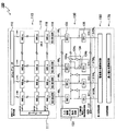
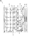
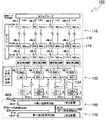
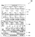
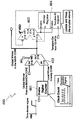
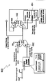
- FIG. 1 is a configuration diagram of a memory device according to a first embodiment of the present invention. It is a block diagram of the memory device which concerns on the 2nd Embodiment of this invention.
- FIG. 6 is a configuration diagram of a memory device according to a third embodiment of the present invention.
- FIG. 6 is a configuration diagram of a memory device according to a fourth embodiment of the present invention.
- FIG. 9 is a configuration diagram of a memory device according to a fifth embodiment of the present invention.
- FIG. 16 is a block diagram of a memory area that assumes a case where there is one nonvolatile memory grain and a power driver is provided for each dimension of reference data in the implementation example illustrated in FIG. 15.
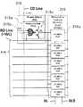
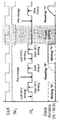
- FIG. 4 is a circuit diagram of 4T-2MTJ memory cells in a memory unit. 19 is a time chart for explaining the operation of the 4T-2MTJ memory cell shown in FIG.
- FIG. 16 is a block diagram of a read / write circuit in the implementation example shown in FIG. 15.
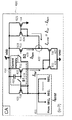
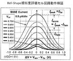
- FIG. 16 is a circuit diagram of a similarity evaluation cell in the mounting example shown in FIG. 15.
- FIG. 16 is a circuit diagram of a current integration circuit in the mounting example shown in FIG. 15.
- FIG. 16 is a circuit diagram of a time domain converter in the implementation example shown in FIG. 15.
- FIG. 4 is a circuit diagram of 4T-2MTJ memory cells in a memory unit. 19 is a time chart for explaining the operation of the 4T-2MTJ memory cell shown in FIG.
- FIG. 16 is a block diagram of a read / write circuit in the implementation example shown in FIG. 15.
- FIG. 16 is a circuit diagram of a similarity evaluation cell in the mounting example shown in FIG. 15.
- FIG. 16 is
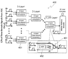
- FIG. 16 is a block diagram of a TD-WTA circuit in a search unit in the implementation example shown in FIG. 15.
- FIG. 16 is a configuration diagram of a minimum value comparison / update circuit in the mounting example shown in FIG. 15, and shows a configuration used in a branch core.
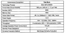
- FIG. 16 is a configuration diagram of a minimum value comparison / update circuit in the implementation example shown in FIG. 15 and is used in the main core. It is an image which shows the photograph of the chip
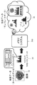
- FIG. 1A is a diagram for explaining a scene where a memory device 100 according to an embodiment of the present invention is applied.
- the search data 10 is converted into feature vector data 20 of one or more dimensions.
- the converted data includes N ( ⁇ 1) -dimensional feature vector data 20, and one dimension has M ( ⁇ 1) bits.
- the memory device 100 extracts the most similar data from the stored reference data 30.
- the memory device 100 includes a memory area as will be described later.
- FIG. 1B is a diagram for explaining a scene where the memory system 200 according to the embodiment of the present invention is applied.
- the search data 10 when search data 10 is input, the search data 10 is converted into feature vector data 20 of one or more dimensions.
- the converted data includes N ( ⁇ 1) -dimensional feature vector data 20, and one dimension has M ( ⁇ 1) bits.
- the memory system 200 extracts the most similar data from the reference data 30 stored in each memory device.
- the memory device has a memory area as will be described later.
- search data 10 feature vector data 20, and reference data 30 will be described.
- Search data 10 is also called target data, and refers to data that is input with respect to data to be searched from data stored in the memory area.
- the reference data 30 is also referred to as template data, and is data stored in the memory area and is data to be searched by the search data.
- Search data 10 and reference data 30 are subject to image data, sound data, text data (sentence data), and of any kind.
- the natural numbers M and N are set according to the type of target data.
- the feature vector data 20 extracts N ( ⁇ 1) feature quantities from a number of viewpoints, indicates the ratio of one feature quantity as a number (this number is expressed in M bits), and includes N feature quantities. This means the ratio displayed in vector.
- the number of features is called the number of dimensions.
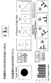
- FIG. 2 is an explanatory diagram of the feature vector data 20.
- the search data is indicated by how much each color of RGB is included.
- the contour included in the search data 10 is along each reference contour as shown in “4-Direction Edge Map”. It is determined whether or not a part is included, and the part along each reference contour is counted by the number of pixels as shown in “Edge Distribution”, and dotted lines of 0 °, 45 °, 90 °, and ⁇ 45 °
- the distribution of the number of pixels in each part divided by is created and shown as a distribution like an eight-dimensional feature vector (“8-D Feature Vector”) as shown in “Vector Generation”.
- the feature vector data 20 is not limited to the simple one shown in FIG. 2 and may be complex feature vector data.
- the 128-dimensional scale-invariant feature transform (SIFT) or Bag- It may be vector data of of-feature (Bof).
- the memory grain is a memory subarray that stores one-dimensional data (M bits) of the reference data 30.
- fine-grain power gating is performed on the memory grain, and power control (ON / OFF) is performed independently.
- “Local winner” is the reference data most similar to the search data among the reference data for one line in the memory area.
- the memory area refers to a memory unit in a memory device
- in the memory system refers to a memory unit in a core including both a main core and a branch core.
- the local winner is obtained in a search unit of a memory device (also referred to as a core).
- “Local Winner Similarity” is the similarity between local winner and search data.
- the local winner similarity is obtained, for example, as a current value in each search unit, and is converted into the number of clock cycles by a counter in each search unit.
- the global winner is the reference data selected from the local winner, and is the reference data most similar to the search data in all the reference data stored in the memory area.
- the global winner is calculated by the comparison / update circuit, the similarity is compared with the local winner, and the global winner is updated to a higher similarity.
- the global winner is calculated only by the comparison update circuit of the main core, the similarity is compared with the local winner, and the global winner is updated to a higher similarity.
- Global Winner Similarity is the similarity between the global winner and the search data. In order to update the global winner, it is temporarily stored in a temporary storage circuit such as the register of the comparison update circuit together with the address of the global winner, and is higher compared to the local winner similarity entered at an off-timing Things are rewritten. In the memory device, calculation is performed by the comparison / update circuit, and in the memory system, calculation is performed only by the comparison / update circuit of the main core.
- M-bit data is stored as reference data for each dimension in the memory area.
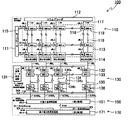
- FIG. 3 is a configuration diagram of the memory device according to the first embodiment of the present invention.
- the memory device 100 according to the embodiment of the present invention includes a memory unit 110, a similarity evaluation unit 130, a search unit 150, and a comparison / update unit 170.
- the memory unit 110 also called a reference data storage circuit, includes a row decoder 111, a column decoder 112, a memory area 113, and a read / write circuit 114, and writes and reads reference data to and from a memory grain 119 in the memory area 113. It is configured to be able to.
- a plurality of reference data having N ( ⁇ 1) dimensions and one dimension having M ( ⁇ 1) bits are stored separately for each dimension.
- the memory area 113 is provided with an arbitrary number (however, 1 ⁇ k ⁇ N) of memory grains (MG) 119 constituting an M-bit memory as one unit.
- MG memory grains
- FIG. 3 shows a case where the arbitrary number k is 1.
- the similarity evaluation unit 130 includes at least an input search data storage circuit 131, a plurality of similarity evaluation cells (SEC: Similarity Evaluation Cell) 133, and a current integration circuit (CA: Current Accumulator) 135.
- SEC Similarity Evaluation Cell
- CA Current Accumulator
- the input search data storage circuit 131 stores search data having N ( ⁇ 1) dimensions and one dimension consisting of M ( ⁇ 1) bits, and is stored in each column of the memory area 113. In response, the search data is output separately.
- Each similarity evaluation cell 133 outputs, as a similarity current value, whether the data read from the input search data storage circuit 131 is similar to the reference data read by the corresponding read / write circuit 114.
- the “data read from the input search data storage circuit 131” (referred to as “first data”) is data output from the input search data storage circuit 131 after the search data is decomposed for each dimension. Yes, the voltage value of the search data for each number of dimensions.
- “Reference data read by the corresponding read / write circuit 114” (referred to as “second data”) is a voltage value of the reference data input from the read / write circuit 114.
- the first data and the second data are evaluated to be the same, and when the current value is large, the first data and the second data are evaluated to be different. That is, if the search data and the reference data are similar, the output current value becomes small.
- Each current integration circuit (CA) 135 integrates the current output from the corresponding arbitrary number of similarity evaluation cells 133.
- Each current integration circuit 135 receives a current value from an arbitrary number of corresponding similarity evaluation cells 133, and determines whether the reference data is similar to the search data based on the current.
- the search unit 150 receives the current values output from the plurality of current integration circuits 135, detects the current related to the reference data most similar to the search data, that is, the current related to the similarity, and uses the detected value as predetermined data. Convert to The comparison / update unit 170 compares and updates the reference data most similar to the search data among the reference data stored in the memory area 113 with respect to the reference data read from the memory area 113 for each row.
- each of the current integration circuits 135 integrates the current from the similarity evaluation cell 133 in accordance with the number of dimensions and an arbitrary number of reference data stored in the memory area 113. Therefore, it is possible to flexibly cope with the number of dimensions of the reference data. Also, the similarity evaluation cell 133 and the current integration circuit 135 are realized with a relatively simple circuit configuration.
- the memory area 113 is composed of a memory cell array of (R ⁇ M) rows and C columns, and is configured as a reference data storage circuit that stores (R ⁇ C) / N reference data.
- the memory device 100 includes C similarity evaluation cells 133, and calculates the similarity between C / N reference data and search data in parallel and outputs the same as a current.
- the current integration circuit 135 integrates C similarity currents according to the number of dimensions of the reference data.
- the similarity evaluation unit 130 includes a changeover switch 134 for each column.
- the changeover switch 134 is configured such that the first switch 134a and the second switch 134b are interlocked.
- the first switch 134a includes a wiring line between the j-th column similarity evaluation cell 133 and the j-th column current integration circuit 135, a (j + 1) -th column similarity evaluation cell 133, and a (j + 1) -th column. It is provided between the second current integration circuit 135 and the wiring.
- j is a natural number of 1 or more (maximum number of columns ⁇ 1).
- the second switch 134b is provided between the similarity evaluation cell 133 and the current integration circuit 135 in each column.
- the first switch 134a and the second switch 134b are both controlled by an external dimension control signal (DCS: Dimension Control Signal), and the line to which the external dimension control signal is input is the first switch A NOT circuit 134c is included between any of the wirings connected to either the control electrode 134a or the control electrode of the second switch 134b.
- DCS Dimension Control Signal
- the dimension control signal controls the changeover switch 134 corresponding to the dimension of the reference data stored in the memory area 113.
- each of the current integration circuits 135 can integrate the current from the similarity evaluation cell 133 in accordance with the number of dimensions and an arbitrary number of reference data stored in the memory area 113. And can flexibly correspond to the number of dimensions of the reference data.
- FIG. 4 is a configuration diagram of the memory device 100 according to the second embodiment of the present invention.
- the memory device 100 shown in FIG. 4 is designed and manufactured with an arbitrary number k of 2 unlike the configuration of the similarity evaluation unit 130 shown in FIG.
- a plurality of similarity evaluation cells 133 are divided into cell groups. As shown in FIG. 4, the odd-numbered column similarity evaluation cells 133 and the even-numbered similarity evaluation cells 133 constitute a cell group 133a.
- the current integration circuit 135 corresponds to one cell group 133a.
- a changeover switch 134 is provided so that the current integration circuit 135 integrates the currents output from any number of similarity evaluation cells 133 in a cell group 133a different from the corresponding one cell group 133a. ing.
- the selector switch 134 is not provided for each column, and one similarity evaluation cell 133 in the odd column and one similarity evaluation cell 133 in the even column are provided.
- the cell group 133a is configured, and the second switch 134b is provided between one similarity evaluation cell 133 in the even-numbered column and the current integration circuit 135 corresponding to the cell group 133a, and the first switch 134a is provided between the cell group 133a and the adjacent cell group 133a.
- the similarity currents from the four similarity evaluation cells 133 can be integrated by turning on one of the first switch 134a and the second switch 134b and turning off the other.
- the similarity currents from the single similarity evaluation cells 133 can also be integrated.
- the cell group includes two similarity evaluation cells 133, but any number of three or more may be used. Thereby, it can respond flexibly also by numbers other than the order of search data and reference data.
- the arbitrary number of similarity evaluation cells 133 in the cell group may be set to be equal to the arbitrary number of memory grains 119 supplied by one power driver 118 shown in FIG. 7, as will be described later.
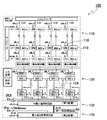
- FIG. 5 is a structural diagram of the memory device 100 according to the third embodiment of the present invention, and more specifically shows the configuration shown in FIG.
- the similarity evaluation unit 130 includes an input search data storage circuit 131, a digital / analog converter (DAC) 132, C / N reference data, and search data.
- C similarity evaluation cells 133 that calculate the similarity in parallel and output the current, a changeover switch 134, and a current integration circuit (CA) 135 that integrates the C similarity currents according to the number of dimensions of the reference data.
- CA current integration circuit
- TDC time domain converter
- the memory area 113 is composed of a memory cell array of (R ⁇ M) rows and C columns, and a reference data storage circuit that stores (R ⁇ C) / N reference data is provided. Yes.
- Digital / analog converter 132 Similarity evaluation cell 133, changeover switch 134, current integration circuit 135, and time domain converter 136 are provided as many as the number of column lines. For each column, digital data is input as a voltage value from the read / write circuit 114 to the digital / analog converter 132, and the digital data is converted into analog data in the digital / analog converter 132 and output to the similarity evaluation cell 133.
- the similarity evaluation cell 133 calculates the similarity between the two input data.
- the first data is data output from the input search data storage circuit 131 after the search data is decomposed for each dimension, and is a voltage value of the search data for each number of dimensions.
- the second data is the voltage value of the reference data input from the read / write circuit 114 via the digital / analog converter 132.
- the similarity evaluation cell 133 calculates and outputs the similarity between the first data and the second data as a current value. When the current value is zero, the first data and the second data are evaluated to be the same, and when the current value is large, the first data and the second data are evaluated to be different. That is, when the reference data is similar to the search data, the output current value is small.
- a changeover switch 134 is provided for each column.
- the changeover switch 134 is configured such that the first switch 134a and the second switch 134b are interlocked.
- the first switch 134 a is provided between the j-th column-th similarity evaluation cell 133 and the (j + 1) -th column similarity evaluation cell 133.
- j is a natural number greater than or equal to 1 (number of columns minus 1).
- the function of the selector switch 134 in FIG. 5 is the same as that of the selector switch 134 in FIG.
- the second switch 134b is provided between the similarity evaluation cell 133 and the current integration circuit 135 in each column.
- the first switch 134a and the second switch 134b are both controlled by an external dimension control signal (DCS: Dimension Control Signal), and the line to which the external dimension control signal is input is the first switch A NOT circuit 134c is included between any of the wirings connected to either the control electrode 134a or the control electrode of the second switch 134b.
- DCS Dimension Control Signal
- the dimension control signal controls the changeover switch 134 corresponding to the dimension of the reference data stored in the memory area 113.
- N-dimensional reference data is stored separately from memory glen MG i j to memory glen MG i j + n ⁇ 1 , is the N-dimensional reference data similar to the search data? Is evaluated, the similarities from the jth-th similarity evaluation cell SEC j to the (j + N ⁇ 1) th-th similarity evaluation cell SEC j + N ⁇ 1 need to be added.
- the first switch 134a is provided between the jth-th similarity evaluation cell SEC j and the (j + 1) th-th similarity evaluation cell SEC j + 1.
- the second switch 134b is provided between the j-th column similarity evaluation cell SEC j and the j-th column current integration circuit CA j .
- the first switch 134a is connected to the N similarity evaluation cells 133 by an external dimension control signal.
- a voltage of search data for each dimension is applied to the input terminal of the similarity evaluation cell 133, the current value output from the similarity evaluation cell 133 is input to the current integration circuit 135, and is temporarily stored in the current integration circuit 135.
- the voltage of the reference data for each dimension is applied to the input terminal of the similarity evaluation cell 133, the current value output from the similarity evaluation cell 133 is input to the current integration circuit 135, and the stored current value and Calculate the difference between In this way, by the cooperation between the similarity evaluation cell 133 and the current integration circuit 135, whether or not the reference data distributed and stored in a plurality of columns is similar to the search data can be obtained from the current value.
- the time domain converter 136 converts the current value output from the current integration circuit 135 into a delay time. Therefore, by inputting the current value to the time domain converter 136 from the similarity evaluation cell 133 having the largest column number among the similarity evaluation cells 133 connected by the changeover switch 134 (for example, the right end), Whether or not the reference data distributed and stored in a plurality of columns is similar to the search data can be obtained as a time delay value. The higher the similarity, the smaller the time delay value. Any of the converted delay time signals is input to the search unit 150.
- the search unit 150 includes a TD (Time Domain) minimum value search circuit 151 that detects the shortest value from the C / N time domain voltage delay signals and converts the shortest delay into the minimum number of clocks using a counter.
- the TD minimum value search circuit 151 searches for the shortest time delay signal among the time delay signals input from the time domain converters 136 in the similarity evaluation unit 130, that is, the minimum value of the time domain.
- the searched value with the shortest delay time is counted by a W-bit counter, and the count value is output to the comparison / update unit 170.
- the comparison / update unit 170 includes a minimum value comparison / update circuit 171 that compares the obtained minimum number of clocks with the previously calculated number of clocks and updates the smaller one.
- the minimum value comparison / update circuit 171 compares the count value input from the search unit 150 with the count value stored by itself every time reading of the memory unit 110 is repeated, and stores the lower count value. Thereby, when the reading of the memory unit 110 is repeated, a low count value is obtained, and as a result, the count value of the reference data most similar to the search data is obtained. By making this count value correspond to the address of the memory unit 110, the address of the most similar reference data in the memory unit 110 is obtained.
- the input search data storage circuit 131 divides the input search data for each dimension, converts it into an analog voltage by the digital / analog converter 132, and inputs it to the similarity evaluation cell 133.
- one-dimensional reference data (M bits) respectively output from the C memory grains 119 via the read / write circuit 114 is similarly converted into an analog voltage by the digital / analog converter 132, and the search data Are input to the C similarity evaluation cells 133 in parallel. If the digital / analog converter 132 is serial, it takes M clock time to convert M-bit data.
- the similarity evaluation cell 133 outputs the similarity between the voltage of the search data (one-dimensional) and the voltage of the reference data (one-dimensional) as a current for each dimension.
- the external dimension control signal controls the first switch 134a between the similarity evaluation cells 133 to be in the ON state according to the number of dimensions of the reference data and the search data,
- the currents of the similarity evaluation cells 133 in which the switch 134a is in the ON state are added, and the currents of the C similarity evaluation cells 133 are integrated by the C / N current integration circuits 135 to correspond to the corresponding time domain converter 136. Output to.
- the second switch 134b is turned off and invalidated so as not to connect the unnecessary current integration circuit 135 and the time domain converter 136.
- the time domain converter 136 converts the integrated C / N similarity currents into a time domain voltage delay signal, and in parallel a minimum value search circuit (time domain (TD) minimum value search circuit as a search circuit) ) Output to 151.
- TD time domain
- a minimum value search circuit (time domain (TD) minimum value search circuit) 151 uses a time domain corresponding to C / N reference data for one row.
- the voltage delay signal having the highest similarity, that is, the one having the shortest delay is obtained, the delay is converted into a digital value which is the number of clocks being delayed by a W-bit counter, and output to the minimum value comparison / update circuit 171.
- the W-bit counter is converted into a time domain voltage delay signal having a maximum delay of 2 W clock, and a resolution of similarity current conversion proportional to the maximum delay is obtained. That is, if W is large, a smaller similarity current difference can be obtained.
- the minimum value comparison / update circuit 171 inputs the digital delay value of the Winner (local Winner) obtained by the main core 210 or the branch core 220.
- the digital delay value of the Winner (local Winner) is compared with the values of all steps stored in the circuit, and the smaller one is rewritten and updated.
- the most similar data from all the reference data in the main core 210 and the branch core 220 is finally stored in the minimum value comparison / update circuit 171 and becomes an associative process result.
- the main core 210 and the branch core 220 will be described in detail with reference to FIG.
- FIG. 6 is a configuration diagram of a memory device according to the fourth embodiment of the present invention, and is a configuration diagram illustrating a specific form of the memory device 100 of FIG.
- a digital / analog converter 132 is provided in front of each similarity evaluation cell 133.
- the digital / analog converter 132 converts the input digital voltage into an analog voltage and outputs the analog voltage to the similarity evaluation cell 133.
- a time domain converter 136 is provided after the current integration circuit 135, and the time domain converter 136 converts the current value output from the current integration circuit 135 into a delay time.
- the current value from the similarity evaluation cell 133 at the extreme end is input to the time domain converter 136, thereby being distributed in a plurality of columns. Whether the reference data stored in this manner is similar to the search data can be obtained as a time delay value.
- a digital / analog converter 132 is provided in the preceding stage of the similarity evaluation cell 133, and the similarity evaluation cell 133 evaluates the similarity based on the data converted by the digital / analog converter 132.
- An analog current is obtained as a value to be obtained and output to the current integration circuit 135, and whether or not the reference data is similar to the search data is obtained as a difference between the current values.
- the digital / analog converter 132 in the preceding stage of the similarity evaluation cell 133, and it may be as follows.
- the digital voltage value of the search data and the digital voltage value of the reference data are sequentially input to the similarity evaluation cell 133, and a digital value for evaluating the similarity is obtained in the similarity evaluation cell 133. It may be converted into an analog value by a digital / analog converter (not shown) provided at a subsequent stage and output to the current integration circuit 135.
- the similarity evaluation cell 133 may be used by appropriately changing a circuit used in the digital approach.
- the output from the current integration circuit 135 is converted into a delay time by the time domain converter 136 to obtain the shortest delay time.
- the embodiment of the present invention is not limited to this, and may be as follows.
- a circuit that directly compares and updates the minimum value of the analog voltage while maintaining the analog value is provided, or a circuit that converts the minimum value of the analog voltage into a digital value and a circuit that compares and updates the digital value.
- an analog current flowing from each current integration circuit may be converted into an analog voltage by connecting each resistor to an output terminal from each current integration circuit, and a minimum value may be searched for among the voltages.
- the search unit 150 shown in FIGS. 3 to 6 may be configured by an analog voltage minimum value search circuit. A specific example of the analog voltage minimum value search circuit will be described later with reference to FIG.
- FIG. 7 is a configuration diagram of a memory device according to the seventh embodiment of the present invention, and is a diagram for explaining details of a memory unit in the memory device 100.
- the memory unit 110 includes a reference data storage circuit configured of a memory cell array of (R ⁇ M) rows and C columns and storing (R ⁇ C) / N reference data.
- 7 is a configuration diagram corresponding to FIG. 5, but other configurations shown in FIGS. 3, 4, and 6 can be adopted.
- the reference data storage circuit as the memory unit 110 has a memory grain (MG: Memory Grain) 119 for storing one-dimensional data of R ⁇ C (C ⁇ N), and each memory grain 119 has an M-bit value. Is saved.
- Each memory glen 119 is provided with a power driver (PD: Power Driver) 118 for power gating, and the power driver 118 controls power supply independently by a row decoder, a column decoder, and a clock 1 (clk.1). That is, C / N pieces of reference data are stored in one line of memory glen (MG) 119, and each reference data is output in parallel to the similarity evaluation cell 133 to perform associative recognition.
- PD Power Driver
- the reference data storage circuit as the memory unit 110 includes a row decoder 111, a column decoder 112, a memory area 113, and a read / write circuit 114.
- the memory area 113 includes a plurality of row lines 115, a plurality of bit lines 116, a plurality of column lines 117, a plurality of power drivers (PD) 118, and a plurality of memory grains (MG) 119.
- the memory glen 119 is composed of a nonvolatile memory.
- a plurality of row lines 115 are connected to the row decoder 111, and a plurality of column lines 117 are connected to the column decoder 112.
- the memory area 113 is divided into a plurality of areas, and each area is designated by an arbitrary number of column lines 117 and M row lines 115 of 1 to N, and a power driver 118 and a memory glen 119 are combined for each area.
- the arbitrary number of column lines 117, the number of row lines 115, and the number of bit lines 116 are all set at the time of design and manufactured according to the settings.
- the “arbitrary number” includes a case where it is determined by a user who uses the memory device, and also includes a case where it is simply determined to be a constant value at the time of design / manufacturing.
- FIG. 7 there are one column line 117, M row lines 115, and M bit lines 116 for each region.
- the definitions of the natural numbers M and N are the same as the definitions in the search data 10 and the reference data 30 described above with reference to FIGS.
- a memory glen 119 configured with an M-bit non-volatile memory as one unit;
- a power driver 118 that supplies power to the memory glen 119 is provided as a set.
- the “arbitrary number” includes a case where it is determined by a user who uses the memory device. This includes cases where it is determined. It is equal to an arbitrary number of memory grains 119 for each area, and is one in FIG.
- a certain power driver 118 receives a control signal input from any number of column lines 117, a control signal input from M row lines 115, and a clock signal input. In response to the clock signal, power is supplied to the memory glen 119 paired with the power driver 118. As a result, the reference data for each dimension stored in the memory glen 119 is read out and output to the read / write circuit 114 of the column through the bit line 116.
- the memory grain 119 has R rows and C columns from MG 11 to MG RC , one or a plurality of row lines 115 through which a control signal from the row decoder 111 flows, and from the column decoder 112
- one or a plurality of power drivers 118 are designated by one or a plurality of column lines 117 through which a control signal flows, and when the clock signal “1” is inputted to the designated power driver 118, only while the power signals are inputted.
- Power is supplied from the power driver 118 to the memory glen 119 as a set.
- the clock signal “0” is input to the designated power driver 118, the supply of power to the memory glen 119 that forms a set is stopped.
- the power driver 118 supplies power to the pair of memory grains 119 when the clock signal “0” is input, and does not supply power to the pair of memory grains 119 when the clock signal “1” is input. You may do it.
- the clock signals “0” and “1” correspond to “H” and “L”.
- control signals from the M row lines 115 may be input in order for a predetermined number of 1 to M lines, or may be simultaneously applied to 1 to M lines.
- FIG. 8 to 10 are diagrams for comparing the memory unit in the memory device according to the embodiment of the present invention, its operation, and power consumption with those of the prior art.
- FIG. 8 is a diagram schematically showing a memory unit, its operation, and power consumption in the memory device according to the fifth embodiment of the present invention.
- the upper part of FIG. 8 schematically shows the memory unit 110, and the middle part of FIG. 8 shows the data read out from which region when Data # 1, Data # 2, and Data # 3 are read out in order for each row.
- a power driver 118 is provided for each dimension of the reference data (for each memory grain), and not only fine-grained power gating is used, but also a plurality of arbitrary column lines 117 can be activated simultaneously in 1 Data. Power is flexibly supplied only to the necessary memory glen 119 corresponding to the required data dimension. Further, a clock signal for operation calculation is input to the power driver 118, and power is supplied from the power driver 118 to the corresponding memory glen 119 in synchronization with the clock signal.
- This read control consumes power only when the data required for computation is in computation, and does not consume power when no clock signal for computation is entered. Furthermore, power is consumed only when the clock pulse is “0” during reading. When the clock pulse is “1” (the first half of the clock), pre-charge, that is, the bit line 116 is precharged to 0 V, it is not necessary to supply power, and the power consumption during the arithmetic operation is halved.
- the data # 1 (Data # 1) uses a clock when data of all dimensions of the reference data is required, so that the power consumption is halved during reading.
- the reason is as follows. With the introduction of clock control, when the first half of one clock, that is, when the clock signal is “H”, the memory glen 119 is not supplied with power but is precharged. When the second half of one clock, that is, when the clock signal is “L”, power is supplied to the designated memory glen 119 to read data. This precharge prevents data from being rewritten when reading the reference data in order to prevent disturb malfunctions when switching the power supply at high speed.
- Data # 3 when data output of a dimension of a part of the reference data is necessary, power can be supplied to only the minimum necessary memory glen 119 to optimize power consumption.
- the memory unit 110 is configured by a non-volatile memory based on power gating capable of cycle-based granularity control. With this configuration, power consumption during standby is reduced to zero, power is supplied to necessary portions of the memory unit 110, and power is not supplied to unnecessary portions, so that power consumption can be reduced.
- Non-volatile memory has been developed with emphasis on various performances such as small area, high speed, high stability, and low write current, but here, it realizes power gating capable of cycle-based fine grain control Therefore, a high-speed and stable nonvolatile memory cell is necessary.
- power gating capable of high-speed search and cycle-based granularity control can be realized for the following reason.
- a differential pair type STT-MRAM memory cell for example, a 4T-2MTJ cell
- the 4T-2MTJ cell is characterized in that it can read data from the MTJ faster and does not cause disturb malfunction due to high-speed power ON / OFF.
- pre-charge is performed to 0 V so as not to accumulate a disturbing charge on the bit line.
- ultra-low power of the associative memory can be achieved by a nonvolatile memory device based on power gating capable of cycle-based granularity control.
- the system is reconfigured according to the number of data dimensions by the changeover switch 134 of the similarity evaluation unit 130, the non-volatile memory device based on power gating capable of cycle-based granularity control is the minimum necessary depending on the reconfiguration. Since power is supplied to a limited memory, power consumption during operation can be optimized.
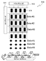
- FIG. 9 is a diagram schematically showing the memory unit 510, its operation, and power consumption in the conventional approach.
- the upper part of FIG. 9 schematically shows the memory unit 510, and the middle part of FIG. 9 reads data from which row area when Data # 1, Data # 2, and Data # 3 are sequentially read for each row. Indicate.
- the horizontal axis indicates time
- the vertical axis indicates power consumption
- the depth axis indicates the position of memograins.
- the memory area of the memory unit 510 is composed of a volatile SRAM. Therefore, it is necessary to always supply power to all the memory grains 519 when writing reference data, reading data # 1, reading data # 2, and reading data # 3. .
- Reference numeral 511 is a row decoder
- reference numeral 512 is a column decoder.
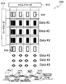
- FIG. 10 is a diagram schematically showing a memory unit composed of a conventional STT-MRAM, its operation and power consumption.
- the upper part of FIG. 10 schematically shows the memory unit 610, and the middle part of FIG. 10 shows the data read out from the region of which row when Data # 1, Data # 2, and Data # 3 are sequentially read out for each row.
- a power driver 618 is provided for each reference data of 1 Data, that is, for every N memory grains 619, using a fine-grain power gating technique, and independent power can be supplied. Therefore, the access reference data specified by the addresses of the column decoder and the row decoder is also used when writing reference data, reading data # 1, reading data # 2, and reading data # 3. It is possible to supply power according to the location of the memory, and there is no need to supply power to an unnecessary memory location. However, since power gating is performed for each data, power is supplied to all the memory grains 619 at the same time in order to read data of all dimensions in one data.
- Reference numeral 611 is a row decoder
- reference numeral 612 is a column decoder.
- FIG. 11A is a diagram illustrating the reconfiguration of the memory device when the reference data is one-dimensional
- FIG. 11B is a diagram illustrating the reconfiguration of the memory device when the reference data is two-dimensional
- FIG. 11 is a diagram illustrating the reconfiguration of the memory device when the reference data is three-dimensional
- FIG. 11D is a diagram illustrating the reconfiguration of the memory device when the reference data is four-dimensional.
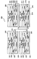
- FIG. 12 is a configuration diagram of a memory system according to the eighth embodiment of the present invention.
- the memory system 200 includes a plurality of memory devices 100, one of which is a main core 210 and the other is a branch core 220. Both the main core 210 and the branch core 220 have the same configuration. That is, each of the main core 210 and the branch core 220 includes reference data storage circuits 211 and 221 as memory units, data adaptive current mode similarity evaluation circuits 212 and 222 as similarity evaluation units, and a search. Time domain minimum value search circuits 213 and 223 as units, minimum value comparison update circuits 214 and 224 as comparison update units, and output buffers 215 and 225.
- Reference data storage circuits 211 and 221 each include a column decoder, a row decoder, a memory glen as a memory area arranged in a matrix, and a write / read circuit.
- a write / read circuit is provided for each memory glen.
- Write or read reference data That is, the reference data storage circuits 211 and 221 write or read the memory Glen reference data for each row.
- the data adaptive current mode similarity evaluation circuits 212 and 222 include at least an input search data storage circuit, a similarity evaluation cell, a current integration circuit, and a time domain converter.
- the search data stored in the input search data storage circuit is divided and input to the similarity evaluation cells of each column, and is read from the memory glen for each column of the reference data storage circuit in the similarity evaluation cell.
- the similarity between the reference data and the search data is evaluated and input to the current integration circuit as a current value.
- the current integration circuit integrates the input current values related to the similarity and outputs them to the time domain converter.
- the time domain converter converts the input current value into a delay time.
- “data adaptive type” means that it can be adapted to the number of dimensions and arbitrary number of search data and reference data, and the details are as described above.
- the time domain minimum value search circuits 213 and 223 as search units receive the current value output from the data adaptive current mode similarity evaluation circuits 212 and 222, and the current related to the reference data most similar to the search data, that is, The current related to the similarity is detected, the detected value is converted into delay time data, and the most similar from each row of the reference data stored in the reference data storage circuits 211 and 221, that is, the similarity Find candidates for high reference data as local winners.
- the minimum value comparison / update circuit 214 as a comparison / update unit is validated only in the main core 210 and compares the reference data most similar to the search data from the reference data read for each row from the reference data storage circuits 211 and 221. Update.
- the candidate of reference data having the highest similarity among the local winners obtained for each read and similarity evaluation by the time domain minimum value search circuits 213 and 223 as the search unit As a global winner, and the similarity of the global winner is stored in the temporary storage circuit.
- the output buffer 225 is enabled only for the branch core 220, temporarily stores the local winner obtained by the time domain minimum value search circuit 223 of the branch core 220, and stores the local winner in the minimum value comparison / update circuit of the main core 210. It is for outputting to 214.
- the main core 210 invalidates the output buffer 215, and the branch core 220 invalidates the minimum value comparison / update circuit 224.
- the invalidated elements are indicated by dotted lines.
- the minimum value comparison / update circuit 214 as a comparison / update unit stores the local winner similarity obtained by the time domain minimum value search circuit 213 as the search unit of the main core 210 and the temporary storage circuit. And the similarity of the local winner calculated by the time domain minimum value search circuit 223 of the search unit of the branch core 220 and the similarity of the global winner stored in the temporary storage circuit. Compare
- the search by the search unit can be performed in parallel with the comparison update, and can be processed in a short time.
- the main core 210 Only the main core 210 enables the minimum value comparison / update circuit 214, and the result of the local Winner (W bit) of the branch core 220 input to the minimum value comparison / update circuit 214 in the pipeline every clock (clock1); Compare the result of your association with the previous step and rewrite it to the smaller one.
- the reference data most similar to the search data is detected from the entire multi-core system.
- the number of chips that can be connected to the multi-core system is determined by the W of the local Winner and the number of bits M of the one-dimensional data.
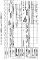
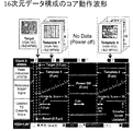
- FIG. 13 is a time chart of main parts of the similarity evaluation unit, the search unit, and the comparison update unit in the memory system shown in FIG.
- FIG. 14 is a diagram for explaining the operation of the memory system 200 shown in FIG.
- One (1 Data) reference data and search data are composed of N ( ⁇ 1) dimension data, and each dimension data is represented by an M-bit digital value.
- the reference data storage circuit as the memory unit 110 includes a memory cell array of (R ⁇ M) rows and C columns, and has a memory glen 119 for storing one-dimensional data of R ⁇ C (C ⁇ N). Each memory grain 119 stores an M-bit value.
- the processing time is more dominant.
- the D / A conversion requires 8-cycle time
- the time domain minimum value search requires 100-200-cycle time. It requires a somewhat long ramp signal in order to achieve a resolution that distinguishes between early and late time domain signals. This is because similarity currents with small differences cannot be distinguished from each other unless the time from 0V to 1V is sufficiently long.
- the similarity is converted into a digital value in the case of a digital approach associative memory, and a current value in the case of the analog approach associative memory and the embodiment of the present invention, so that the difference is small.
- the delay difference of the time domain signal converted from the similarity is small, and it is difficult to distinguish unless measured in a sufficiently long time.
- a pipeline operation based on a multi-core is adopted in order to improve the time-domain minimum value search speed.
- the pipeline absorbs the local long time-domain minimum value search processing time of each core and completes in one clock.
- this multi-core pipeline method is not used, information on similar reference data can be obtained at the same speed as the conventional analog approach associative memory. Further, since the number of dimensions of the reference data and search data can be arbitrarily adjusted, the number of dimensions increases, and the number of memory grains for storing the reference data also increases. If data processing is performed with only one core, as shown in FIG. 14, the “TD minimum value search” processing per line in the memory area takes (2M + 2 W ⁇ 1 ) ⁇ clock, which increases the number of dimensions.
- the number of lines in the memory area to be processed increases.
- the time-domain minimum value search process is performed using a plurality of cores as in the embodiment of the present invention, it is possible to suppress an increase in time for searching for reference data similar to search data.
- FIG. 12 is a configuration diagram of the memory system according to the embodiment of the present invention.
- the memory system 200 includes a plurality of memory devices, one of which is a main core 210 and the other is a branch core 220. Both the main core 210 and the branch core 220 have the same configuration. That is, each of the main core 210 and the branch core 220 includes reference data storage circuits 211 and 221 as memory units, data adaptive current mode similarity evaluation circuits 212 and 222 as similarity evaluation units, and a search. Time domain minimum value search circuits 213 and 223 as units, minimum value comparison update circuits 214 and 224 as comparison update units, and output buffers 215 and 225.
- Reference data storage circuits 211 and 221 each include a column decoder, a row decoder, a memory glen as a memory area arranged in a matrix, and a write / read circuit.
- a write / read circuit is provided for each memory glen.
- Write or read reference data That is, the reference data storage circuits 211 and 221 write or read the memory Glen reference data for each row.
- the data adaptive current mode similarity evaluation circuits 212 and 222 include at least an input search data storage circuit, a similarity evaluation cell, a current integration circuit, and a time domain converter.
- the search data stored in the input search data storage circuit is divided and input to the similarity evaluation cells of each column, and is read from the memory glen for each column of the reference data storage circuit in the similarity evaluation cell.
- the similarity between the reference data and the search data is evaluated and input to the current integration circuit as a current value.
- the current integration circuit integrates the input current values related to the similarity and outputs them to the time domain converter.
- the time domain converter converts the input current value into a delay time.
- “data adaptive type” means that it can be adapted to the number of dimensions and arbitrary number of search data and reference data. For example, a specific configuration of a memory device constituting the main core 210 and the branch core 220 is illustrated in FIG. Details will be described later with reference to FIG.
- the time domain minimum value search circuits 213 and 223 as search units receive the current value output from the data adaptive current mode similarity evaluation circuits 212 and 222, and the current related to the reference data most similar to the search data, that is, The current related to the similarity is detected, the detected value is converted into delay time data, and the most similar from each row of the reference data stored in the reference data storage circuits 211 and 221, that is, the similarity Find candidates for high reference data as local winners.
- the minimum value comparison / update circuit 214 as a comparison / update unit is validated only in the main core 210 and compares the reference data most similar to the search data from the reference data read for each row from the reference data storage circuits 211 and 221. Update.
- the candidate of reference data having the highest similarity among the local winners obtained for each read and similarity evaluation by the time domain minimum value search circuits 213 and 223 as the search unit As a global winner, and the similarity of the global winner is stored in the temporary storage circuit.
- the output buffer 225 is enabled only for the branch core 220, temporarily stores the local winner obtained by the time domain minimum value search circuit 223 of the branch core 220, and stores the local winner in the minimum value comparison / update circuit of the main core 210. It is for outputting to 214.
- the main core 210 invalidates the output buffer 215, and the branch core 220 invalidates the minimum value comparison / update circuit 224.
- the invalidated elements are indicated by dotted lines.
- the minimum value comparison / update circuit 214 as a comparison / update unit stores the local winner similarity obtained by the time domain minimum value search circuit 213 as the search unit of the main core 210 and the temporary storage circuit. And the similarity of the local winner calculated by the time domain minimum value search circuit 223 of the search unit of the branch core 220 and the similarity of the global winner stored in the temporary storage circuit. Compare
- the search by the search unit can be performed in parallel with the comparison update, and can be processed in a short time.
- the main core 210 Only the main core 210 enables the minimum value comparison / update circuit 214, and the result of the local Winner (W bit) of the branch core 220 input to the minimum value comparison / update circuit 214 in the pipeline every clock (clock1); Compare the associative result of the previous step and rewrite and update it to the smaller one.
- the reference data most similar to the search data is detected from the entire multi-core system.
- the number of chips that can be connected to the multi-core system is determined by the W of the local Winner and the number of bits M of the one-dimensional data.
- FIG. 5 is a structural diagram of the memory device 100 serving as a main core and a branch core constituting the memory system of FIG.
- the memory device 100 includes a memory unit 110, a similarity evaluation unit 130, a search unit 150, and a comparison / update unit 170.
- the comparison / update unit 170 may be invalidated.
- the memory unit 110 also called a reference data storage circuit, includes a row decoder 111, a column decoder 112, a memory area 113, and a read / write circuit 114, and writes and reads reference data to and from a memory grain 119 in the memory area 113. It is configured to be able to.
- a plurality of reference data having N ( ⁇ 1) dimensions and one dimension having M ( ⁇ 1) bits are stored separately for each dimension.
- the memory area 113 is provided with an arbitrary number (however, 1 ⁇ k ⁇ N) of memory grains (MG) 119 constituting an M-bit memory as one unit.
- MG memory grains
- FIG. 5 shows a case where the arbitrary number k is 1.
- the similarity evaluation unit 130 calculates the similarity between the input search data storage circuit 131, the digital / analog converter (DAC: Digital Analog Converter) 132, the C / N reference data and the search data in parallel, and outputs it as a current.
- C similarity evaluation cells Similarity Evaluation Cell
- changeover switch 134 a changeover switch 134
- CA Current Accumulator
- TDC time domain converter
- Digital / analog converter 132 Similarity evaluation cell 133, changeover switch 134, current integration circuit 135, and time domain converter 136 are provided as many as the number of column lines. For each column, digital data is input as a voltage value from the read / write circuit 114 to the digital / analog converter 132, and the digital data is converted into analog data in the digital / analog converter 132 and output to the similarity evaluation cell 133.
- the similarity evaluation cell 133 calculates the similarity between the two input data.
- the first data is data output from the input search data storage circuit 131 after the search data is decomposed for each dimension, and is a voltage value of the search data for each number of dimensions.
- the second data is the voltage value of the reference data input from the read / write circuit 114 via the digital / analog converter 132.
- the similarity evaluation cell 133 calculates and outputs the similarity between the first data and the second data as a current value. When the current value is zero, the first data and the second data are evaluated to be the same, and when the current value is large, the first data and the second data are evaluated to be different. That is, when the reference data is similar to the search data, the output current value is small.
- a changeover switch 134 is provided for each column.
- the changeover switch 134 is configured such that the first switch 134a and the second switch 134b are interlocked.
- the first switch 134 a is provided between the j-th column-th similarity evaluation cell 133 and the (j + 1) -th column similarity evaluation cell 133.
- j is a natural number greater than or equal to 1 (number of columns minus 1).
- the second switch 134b is provided between the similarity evaluation cell 133 and the current integration circuit 135 in each column.
- the first switch 134a and the second switch 134b are both controlled by an external dimension control signal (DCS: Dimension Control Signal), and the line to which the external dimension control signal is input is the first switch A NOT circuit 134c is included between any of the wirings connected to either the control electrode 134a or the control electrode of the second switch 134b.
- DCS Dimension Control Signal
- the dimension control signal controls the changeover switch 134 corresponding to the dimension of the reference data stored in the memory area 113.
- the N-dimensional reference data is the search data. It is necessary to add the similarities from the j- th column similarity evaluation cell SEC j to the (j + N ⁇ 1) -th similarity evaluation cell SEC j + N ⁇ 1. There is.
- the first switch 134a is provided between the jth column-th similarity evaluation cell SEC j and the (j + 1) th column-th similarity evaluation cell SEC j + 1.
- the second switch 134b is provided between the j-th column similarity evaluation cell SEC j and the j-th column current integration circuit CA j .
- the first switch 134a is connected to the N similarity evaluation cells 133 by an external dimension control signal.
- a voltage of search data for each dimension is applied to the input terminal of the similarity evaluation cell 133, the current value output from the similarity evaluation cell 133 is input to the current integration circuit 135, and is temporarily stored in the current integration circuit 135.
- the voltage of the reference data for each dimension is applied to the input terminal of the similarity evaluation cell 133, the current value output from the similarity evaluation cell 133 is input to the current integration circuit 135, and the stored current value and Calculate the difference between In this way, by the cooperation between the similarity evaluation cell 133 and the current integration circuit 135, whether or not the reference data distributed and stored in a plurality of columns is similar to the search data can be obtained from the current value.
- the time domain converter 136 converts the current value output from the current integration circuit 135 into a delay time. Therefore, in the preferred memory device 100, among the similarity evaluation cells 133 connected by the changeover switch 134, the current value is input to the time domain converter 136 from the similarity evaluation cell 133 having the largest column number (for example, the right end). By inputting, it is possible to determine whether or not the reference data distributed and stored in a plurality of columns is similar to the search data as a time delay value. The higher the similarity, the smaller the time delay value. Any of the converted delay time signals is input to the search unit 150.
- the search unit 150 includes a TD (Time Domain) minimum value search circuit 151 that detects the shortest value from the C / N time domain voltage delay signals and converts the shortest delay into the minimum number of clocks using a counter.
- the TD minimum value search circuit 151 searches for the shortest time delay signal among the time delay signals input from the time domain converters 136 in the similarity evaluation unit 130, that is, the minimum value of the time domain.
- the searched value with the shortest delay time is counted by a W-bit counter, and the count value is output to the comparison / update unit 170.
- the comparison / update unit 170 includes a minimum value comparison / update circuit 171 that compares the obtained minimum number of clocks with the previously calculated number of clocks and updates the smaller one.
- the minimum value comparison / update circuit 171 compares the count value input from the search unit 150 with the count value stored by itself every time reading of the memory unit 110 is repeated, and stores the lower count value. Thereby, when the reading of the memory unit 110 is repeated, a low count value is obtained, and as a result, the count value of the reference data most similar to the search data is obtained. By making this count value correspond to the address of the memory unit 110, the address of the most similar reference data in the memory unit 110 is obtained.
- the input search data storage circuit 131 divides the input search data for each dimension, converts it into an analog voltage by the digital / analog converter 132, and inputs it to the similarity evaluation cell 133.
- one-dimensional reference data (M bits) respectively output from the C memory grains 119 via the read / write circuit 114 is similarly converted into an analog voltage by the digital / analog converter 132, and the search data Are input to the C similarity evaluation cells 133 in parallel. If the digital / analog converter 132 is serial, it takes M clock time to convert M-bit data.
- the similarity evaluation cell 133 outputs the similarity between the voltage of the search data (one-dimensional) and the voltage of the reference data (one-dimensional) as a current for each dimension.
- the external dimension control signal controls the first switch 134a between the similarity evaluation cells 133 to be in the ON state according to the number of dimensions of the reference data and the search data,
- the currents of the similarity evaluation cells 133 in which the switch 134a is in the ON state are added, and the currents of the C similarity evaluation cells 133 are integrated by the C / N current integration circuits 135 to correspond to the corresponding time domain converter 136. Output to.
- the second switch 134b is turned off to invalidate the unnecessary current integration circuit 135 and the time domain converter 136 so as not to be connected.
- the time domain converter 136 converts the integrated C / N similarity currents into a time domain voltage delay signal, and in parallel a minimum value search circuit (time domain (TD) minimum value search circuit as a search circuit) ) Output to 151.
- TD time domain
- a minimum value search circuit (time domain (TD) minimum value search circuit) 151 uses a time domain corresponding to C / N reference data for one row.
- the voltage delay signal having the highest similarity, that is, the one having the shortest delay is obtained, the delay is converted into a digital value which is the number of clocks being delayed by a W-bit counter, and output to the minimum value comparison / update circuit 171.
- the W-bit counter is converted to a time domain voltage delay signal with a delay of up to 2 W clocks, and a similarity current conversion resolution proportional to this maximum delay is obtained. That is, if W is large, a smaller similarity current difference can be obtained.
- the minimum value comparison / update circuit 171 inputs the digital delay value of the Winner (local Winner) obtained by the main core 210 or the branch core 220.
- the digital delay value of the Winner (local Winner) is compared with the values of all steps stored in the circuit, and the smaller one is rewritten and updated.
- the most similar data from all the reference data in the main core 210 and the branch core 220 is finally stored in the minimum value comparison / update circuit 171 and becomes an associative process result.
- FIG. 13 is a time chart of main parts of the similarity evaluation unit, the search unit, and the comparison update unit in the memory system shown in FIG.
- FIG. 14 is a diagram for explaining the operation of the memory system 200 shown in FIG.
- One (1 Data) reference data and search data are composed of N ( ⁇ 1) dimension data, and each dimension data is represented by an M-bit digital value.
- the reference data storage circuit as the memory unit 110 includes a memory cell array of (R ⁇ M) rows and C columns, and has a memory glen 119 for storing one-dimensional data of R ⁇ C (C ⁇ N). Each memory grain 119 stores an M-bit value.
- the D / A conversion requires 8-cycle time, but the time domain minimum value search requires 100-200-cycle time. It requires a somewhat long ramp signal in order to achieve a resolution that distinguishes between early and late time domain signals. This is because similarity currents with small differences cannot be distinguished from each other unless the time from 0V to 1V is sufficiently long.
- the similarity is converted into a digital value in the case of a digital approach associative memory, and a current value in the case of the analog approach associative memory and the embodiment of the present invention, so that the difference is small.
- the delay difference of the time domain signal converted from the similarity is small, and it is difficult to distinguish unless measured in a sufficiently long time.
- a pipeline operation based on a multi-core is adopted in order to improve the time-domain minimum value search speed.
- the pipeline absorbs the local long time-domain minimum value search processing time of each core and completes in one clock.
- the comparison update is performed only by the comparison update unit of the main core 210, and the search by the search unit is performed in parallel with the comparison update. Therefore, the comparison update of each core can be processed in the pipeline, and associative calculation is performed on the read reference data for each read with an arbitrary number of clocks, for example, one clock.
- the pipeline method based on the multi-core is not used, information about similar reference data can be obtained at the same speed as the conventional analog approach associative memory.
- the number of dimensions of the reference data and search data can be arbitrarily adjusted, the number of dimensions increases, and the number of memory grains for storing the reference data also increases. If data processing is performed with only one core, as shown in FIG. 14, the “TD minimum value search” processing per line in the memory area takes (2M + 2 W ⁇ 1 ) ⁇ clock, which increases the number of dimensions. Correspondingly, the number of lines in the memory area to be processed increases. However, since the time-domain minimum value search process is performed using a plurality of cores as in the embodiment of the present invention, it is possible to suppress an increase in time for searching for reference data similar to search data.
- main core 210 and the branch core 220 are not configured as the memory device 100 shown in FIG. 5, the memory device 100 as described below with reference to FIGS. 3, 4, 6, 7, etc. It may be. In that case, a design change may be requested
- FIG. 3 is a configuration diagram of a memory device serving as a main core and a branch core constituting the memory system of FIG. Similar to FIG. 5, the memory device 100 includes a memory unit 110, a similarity evaluation unit 130, a search unit 150, and a comparison update unit 170. 5 is different from the configuration shown in FIG. 5 in that the digital / analog converter 132 and the time domain converter 136 are not provided. Note that the function of the selector switch 134 in FIG. 7 is the same as that of the selector switch 134 in FIG.
- FIG. 4 is a configuration diagram of the memory device 100 serving as a main core and a branch core constituting the memory system of FIG. 4 differs from FIG. 3 in the configuration of the similarity evaluation unit 130 and is designed and manufactured with an arbitrary number k of 2.
- a plurality of similarity evaluation cells 133 are divided into cell groups. As shown in FIG. 4, the odd-numbered column similarity evaluation cells 133 and the even-numbered similarity evaluation cells 133 constitute a cell group 133a.
- the current integration circuit 135 corresponds to one cell group 133a.
- a changeover switch 134 is provided so that the current integration circuit 135 integrates the currents output from any number of similarity evaluation cells 133 in a cell group 133a different from the corresponding one cell group 133a. ing.
- the selector switch 134 is not provided for each column, and one similarity evaluation cell 133 in the odd column and one similarity evaluation cell 133 in the even column are provided.
- the cell group 133a is configured, and the second switch 134b is provided between one similarity evaluation cell 133 in the even-numbered column and the current integration circuit 135 corresponding to the cell group 133a, and the first switch 134a is provided between the cell group 133a and the adjacent cell group 133a.
- the similarity currents from the four similarity evaluation cells 133 can be integrated by turning on one of the first switch 134a and the second switch 134b and turning off the other.
- the similarity currents from the single similarity evaluation cells 133 can also be integrated.
- the cell group includes two similarity evaluation cells 133, but any number of three or more may be used. Thereby, it can respond flexibly also by numbers other than the order of search data and reference data.
- the arbitrary number of similarity evaluation cells 133 in the cell group may be set to be equal to the arbitrary number of memory grains 119 supplied by one power driver 118 shown in FIG. 7, as will be described later.
- [Specific configuration of main core and branch core # 4] 6 is a configuration diagram of a memory device serving as a main core and a branch core constituting the memory system of FIG. 12, and is a configuration diagram showing a specific form of the memory device 100 of FIG.
- a digital / analog converter 132 is provided in front of each similarity evaluation cell 133.
- the digital / analog converter 132 converts the input digital voltage into an analog voltage and outputs the analog voltage to the similarity evaluation cell 133.
- a time domain converter 136 is provided after the current integration circuit 135, and the time domain converter 136 converts the current value output from the current integration circuit 135 into a delay time.
- the current value from the similarity evaluation cell 133 at the extreme end is input to the time domain converter 136, thereby being distributed in a plurality of columns. Whether the reference data stored in this manner is similar to the search data can be obtained as a time delay value.
- a digital / analog converter 132 is provided in the preceding stage of the similarity evaluation cell 133, and the similarity evaluation cell 133 evaluates the similarity based on the data converted by the digital / analog converter 132.
- An analog current is obtained as a value to be obtained and output to the current integration circuit 135, and whether or not the reference data is similar to the search data is obtained as a difference between the current values.
- the digital / analog converter 132 in the preceding stage of the similarity evaluation cell 133, and it may be as follows.
- the digital voltage value of the search data and the digital voltage value of the reference data are sequentially input to the similarity evaluation cell 133, and a digital value for evaluating the similarity is obtained in the similarity evaluation cell 133. It may be converted into an analog value by a digital / analog converter (not shown) provided at a subsequent stage and output to the current integration circuit 135.
- the similarity evaluation cell 133 may be used by appropriately changing a circuit used in the digital approach.
- the output from the current integration circuit 135 is converted into a delay time by the time domain converter 136 to obtain the shortest delay time.
- the embodiment of the present invention is not limited to this, and may be as follows.
- a circuit that directly compares and updates the minimum value of the analog voltage while maintaining the analog value is provided, or a circuit that converts the minimum value of the analog voltage into a digital value and a circuit that compares and updates the digital value.
- an analog current flowing from each current integration circuit may be converted into an analog voltage by connecting each resistor to an output terminal from each current integration circuit, and a minimum value may be searched for among the voltages.
- the search unit 150 shown in FIGS. 5, 3, 4, and 6 may be configured by an analog voltage minimum value search circuit.
- a specific example of the analog voltage minimum value search circuit will be described later with reference to FIG. In this case, it is necessary to provide an analog / dental converter that digitally converts the output value.
- FIG. 7 is a block diagram of a memory device having a preferred memory unit.
- the memory unit 110 includes a reference data storage circuit configured of a memory cell array of (R ⁇ M) rows and C columns and storing (R ⁇ C) / N reference data.
- 10 is a configuration diagram corresponding to FIG. 4, but other configurations shown in FIGS. 3, 4, and 6 may be employed.
- the reference data storage circuit as the memory unit 110 has a memory grain (MG: Memory Grain) 119 for storing one-dimensional data of R ⁇ C (C ⁇ N), and each memory grain 119 has an M-bit value. Is saved.
- Each memory glen 119 is provided with a power driver (PD: Power Driver) 118 for power gating, and the power driver 118 controls power supply independently by a row decoder, a column decoder, and a clock 1 (clk.1). That is, C / N pieces of reference data are stored in one line of memory glen (MG) 119, and each reference data is output in parallel to the similarity evaluation cell 133 to perform associative recognition.
- PD Power Driver
- the reference data storage circuit as the memory unit 110 includes a row decoder 111, a column decoder 112, a memory area 113, and a read / write circuit 114.
- the memory area 113 includes a plurality of row lines 115, a plurality of bit lines 116, a plurality of column lines 117, a plurality of power drivers (PD) 118, and a plurality of memory grains (MG) 119.
- the memory glen 119 is composed of a nonvolatile memory.
- a plurality of row lines 115 are connected to the row decoder 111, and a plurality of column lines 117 are connected to the column decoder 112.
- the memory area 113 is divided into a plurality of areas, and each area is designated by an arbitrary number of column lines 117 and M row lines 115 of 1 to N, and a power driver 118 and a memory glen 119 are combined for each area.
- the arbitrary number of column lines 117, the number of row lines 115, and the number of bit lines 116 are all set at the time of design and manufactured according to the settings.
- the “arbitrary number” includes a case where it is determined by a user who uses the memory device, and also includes a case where it is simply determined to be a constant value at the time of design / manufacturing.
- FIG. 7 there are one column line 117, M row lines 115, and M bit lines 116 for each region.
- the definitions of the natural numbers M and N are the same as the definitions in the search data 10 and the reference data 30 described above with reference to FIGS.
- a memory glen 119 configured with an M-bit non-volatile memory as one unit;
- a power driver 118 that supplies power to the memory glen 119 is provided as a set.
- the “arbitrary number” includes a case where it is determined by a user who uses the memory device. This includes cases where it is determined. It is equal to an arbitrary number of memory grains 119 for each area, and is one in FIG.
- a certain power driver 118 receives a control signal input from any number of column lines 117, a control signal input from M row lines 115, and a clock signal input. In response to the clock signal, power is supplied to the memory glen 119 paired with the power driver 118. As a result, the reference data for each dimension stored in the memory glen 119 is read out and output to the read / write circuit 114 of the column through the bit line 116.
- the memory grain 119 has R rows and C columns from MG 11 to MG RC , one or a plurality of row lines 115 through which a control signal from the row decoder 111 flows, and from the column decoder 112
- one or a plurality of power drivers 118 are designated by one or a plurality of column lines 117 through which a control signal flows, and when the clock signal “1” is inputted to the designated power driver 118, only while the power signals are inputted.
- Power is supplied from the power driver 118 to the memory glen 119 as a set.
- the clock signal “0” is input to the designated power driver 118, the supply of power to the memory glen 119 that forms a set is stopped.
- the power driver 118 supplies power to the pair of memory grains 119 when the clock signal “0” is input, and does not supply power to the pair of memory grains 119 when the clock signal “1” is input. You may do it.
- the clock signals “0” and “1” correspond to “H” and “L”.
- control signals from the M row lines 115 may be input in order for a predetermined number of 1 to M lines, or may be simultaneously applied to 1 to M lines.
- FIG. 8 to 10 are diagrams for comparing the memory unit, the operation, and the power consumption in the memory device constituting the main core and the branch core with those of the prior art.
- FIG. 8 is a diagram schematically showing a memory unit, its operation, and power consumption in the memory device constituting the main core and the branch core.
- the upper part of FIG. 8 schematically shows the memory unit 110, and the middle part of FIG. 8 shows the data read out from which region when Data # 1, Data # 2, and Data # 3 are read out in order for each row.
- a power driver 118 is provided for each dimension of the reference data (for each memory grain), and not only fine-grained power gating is used, but also a plurality of arbitrary column lines 117 can be activated simultaneously in 1 Data. Power is flexibly supplied only to the necessary memory glen 119 corresponding to the required data dimension. Further, a clock signal for operation calculation is input to the power driver 118, and power is supplied from the power driver 118 to the corresponding memory glen 119 in synchronization with the clock signal.
- This read control consumes power only when the data required for computation is in computation, and does not consume power when no clock signal for computation is entered. Furthermore, power is consumed only when the clock pulse is “0” during reading. When the clock pulse is “1” (the first half of the clock), pre-charge, that is, the bit line 116 is precharged to 0 V, it is not necessary to supply power, and the power consumption during the arithmetic operation is halved.
- the data # 1 (Data # 1) uses a clock when the output of all dimensions of the reference data is required, so that the power consumption is halved during reading.
- the reason is as follows. With the introduction of clock control, when the first half of one clock, that is, when the clock signal is “H”, the memory glen 119 is not supplied with power but is precharged. When the second half of one clock, that is, when the clock signal is “L”, power is supplied to the designated memory glen 119 to read data. This precharge prevents data from being rewritten when reading the reference data in order to prevent disturb malfunctions when switching the power supply at high speed.
- Data # 3 when data output of a dimension of a part of the reference data is necessary, power can be supplied to only the minimum necessary memory glen 119 to optimize power consumption.
- the memory unit 110 is configured by a non-volatile memory based on power gating capable of cycle-based granularity control. With this configuration, power consumption during standby is reduced to zero, power is supplied to necessary portions of the memory unit 110, and power is not supplied to unnecessary portions, so that power consumption can be reduced.
- Non-volatile memory has been developed with emphasis on various performances such as small area, high speed, high stability, and low write current, but here, it realizes power gating capable of cycle-based fine grain control Therefore, a high-speed and stable nonvolatile memory cell is necessary.
- power gating capable of high-speed search and cycle-based granularity control can be realized for the following reason.
- a differential pair type STT-MRAM memory cell for example, a 4T-2MTJ cell
- the 4T-2MTJ cell is characterized in that it can read data from the MTJ faster and does not cause disturb malfunction due to high-speed power ON / OFF.
- pre-charge is performed to 0 V so as not to accumulate a disturbing charge on the bit line.
- ultra-low power of the associative memory can be achieved by a nonvolatile memory device based on power gating capable of cycle-based granularity control.
- the system is reconfigured according to the number of data dimensions by the changeover switch 134 of the similarity evaluation unit 130, the non-volatile memory device based on power gating capable of cycle-based granularity control is the minimum necessary depending on the reconfiguration. Since power is supplied to a limited memory, power consumption during operation can be optimized.
- FIG. 9 is a diagram schematically showing the memory unit 510, its operation, and power consumption in the conventional approach.
- the upper part of FIG. 9 schematically shows the memory unit 510, and the middle part of FIG. 9 reads data from which row area when Data # 1, Data # 2, and Data # 3 are sequentially read for each row. Indicate.
- the horizontal axis indicates time
- the vertical axis indicates power consumption
- the depth axis indicates the position of memograins.
- the memory area of the memory unit 510 is composed of a volatile SRAM. Therefore, it is necessary to always supply power to all the memory grains 519 when writing reference data, reading data # 1, reading data # 2, and reading data # 3. .
- Reference numeral 511 is a row decoder
- reference numeral 512 is a column decoder.
- FIG. 10 is a diagram schematically showing a memory unit composed of a conventional STT-MRAM, its operation and power consumption.
- the upper part of FIG. 10 schematically shows the memory unit 610, and the middle part of FIG. 10 shows the data read out from the region of which row when Data # 1, Data # 2, and Data # 3 are sequentially read out for each row.
- a power driver 618 is provided for each reference data of 1 Data, that is, for every N memory grains 619, using a fine-grain power gating technique, and independent power can be supplied. Therefore, the access reference data specified by the addresses of the column decoder and the row decoder is also used when writing reference data, reading data # 1, reading data # 2, and reading data # 3. It is possible to supply power according to the location of the memory, and there is no need to supply power to an unnecessary memory location. However, since power gating is performed for each Data, all the memory grains 619 are simultaneously supplied with power in order to read data of all dimensions in one Data.
- Reference numeral 611 is a row decoder
- reference numeral 612 is a column decoder.
- FIG. 11A is a diagram illustrating the reconfiguration of the memory device when the reference data is one-dimensional
- FIG. 11B is a diagram illustrating the reconfiguration of the memory device when the reference data is two-dimensional
- FIG. 11 is a diagram illustrating the reconfiguration of the memory device when the reference data is three-dimensional
- FIG. 11D is a diagram illustrating the reconfiguration of the memory device when the reference data is four-dimensional.
- the memory system 200 may include a main core 210 and one or a plurality of branch cores 220 as follows.
- the main core 210 and the branch core 220 are respectively shown in FIG. Arbitrary configuration in which an M-bit memory is configured as one unit in a memory area 113 in which a plurality of reference data consisting of N ( ⁇ 1) dimensions and one dimension consisting of M ( ⁇ 1) bits is divided and stored for each dimension.
- Each similarity evaluation cell obtains the similarity between each of the reference data read for each reading from the memory area 113 and the search data, and reads corresponding to the data read from the search data storage circuit.
- a plurality of similarity evaluation cells 133 that output the similarity of the reference data read by the circuit as a current value;
- Each current integration circuit 135 integrates a plurality of current integration circuits 135 that integrate the currents output from the corresponding arbitrary number of similarity evaluation cells 133;
- a search unit that obtains a candidate of reference data having a high similarity as a local winner from the similarity of each reference data read from the memory area 113 with each search data (reading from the memory area 113 and similarity evaluation) For example, the time domain minimum value search circuit 213, 223), Is provided.
- the main core 210 obtains, as a global winner, a candidate for reference data having the highest similarity among local winners obtained for each reading and similarity evaluation by the search unit (for example, the time domain minimum value search circuits 213 and 223).
- a comparison update unit (minimum value comparison update circuit) 214 having a temporary storage circuit for storing the similarity of
- a comparison / update unit (minimum value comparison / update circuit) 214 compares the similarity of the local winner obtained by the search unit 223 of the main core 210 with the similarity of the global winner stored in the temporary storage circuit, and the branch core 220.
- the similarity of the local winner obtained by the search unit (for example, the time domain minimum value search circuit 223) is compared with the similarity of the global winner stored in the temporary storage circuit.
- the system can be easily configured with the same compact design core. Secondly, the processing time can be reduced, and secondly, when searching for reference data similar to search data, the number of dimensions of the reference data can be flexibly handled and a compact circuit configuration is provided. Can be satisfied at the same time. Since this system is realized by selecting and combining the above-described embodiments, description thereof will be omitted.
- FIG. 15 is a block configuration diagram according to an implementation example. Assuming its application to image recognition, a low-power, high-density and adaptable nonvolatile associative memory device is assumed. 15 includes a memory unit 310, a similarity evaluation unit 330, a search unit 350, a comparison update unit 370, and a timing controller 390, as in FIG. As in FIG. 7, the memory unit 310 includes a row decoder 311, a column decoder 312, a memory area 313, a read / write circuit 314, a row line 315, a bit line 316, a column line 317, a power driver 318, and a memory glen 319. .
- the similarity evaluation unit 330 includes a digital / analog converter (DAC) 332, a similarity evaluation cell (SEC) 333, a changeover switch 334, a current integration circuit (CA) 335, and a time domain converter (TDC) 336.
- the changeover switch 334 includes a first switch 334a, a second switch 334b, and a negation circuit 334c. This is a prototype chip that assumes 8-dimensional, 16-dimensional, 32-dimensional, 64-dimensional, and 128-dimensional image feature data. Basically, any number of dimensions that is an integer multiple of 8 can be handled.
- Each parameter described with reference to FIG. 7 is as follows.
- N 8 dimensions, 16 dimensions, 32 dimensions, 64 dimensions, and 128 dimensions, and can be applied to dimensions that are integer multiples of 8.
- M 8 bits
- C 128 columns
- R 16 rows
- W 8 bits (the number of bits of the counter of the minimum value comparison / update circuit)
- both the PD of the memory Glen and the integrated switch of the similarity current are designed every 8 dimensions.
- FIG. 16 is a block diagram of each memory area in the implementation example.
- FIG. 16 shows one area of the memory area described with reference to FIG.
- the logical operation circuit 318b of the power line gate 318a receives one of a column line (CD Line), a clock signal input line, and a row line (RD Line). It is input to the arithmetic circuit 318b.
- the output signal from the logic operation circuit 318b is input to the inverter circuit 318c connected to the power supply line.
- the output from the inverter circuit 318c is input to the 4T-2MTJ cell 319a as the power line PL.
- BL and BLB are a pair of bit lines.
- FIG. 17A is a diagram assuming a case in which one nonvolatile memory grain 319 is provided in the block diagram of FIG. 16 and a power driver 318 is provided for each dimension of reference data.
- FIG. 17B is a time chart showing an operation of continuously reading data from two 4T-2MTJ memory cells (Cell # 1 and Cell # 2) for the unit shown in FIG. 17A. As described above, in the read operation, when the clock signal is “0”, CD Line is “1”, and the corresponding RD Line is also “1”, the power line PL is “1”. And reading processing is in progress.
- FIG. 17C is a modification of the circuit shown in FIG. 17A, and the power line PL may be output to each of the M 4T-2MTJ cells 319a in parallel from one power line gate.
- FIG. 18 is a circuit diagram of the 4T-2MTJ memory cell 320 in the memory unit 310.
- the 4T-2MTJ memory cell 320 is a differential pair type STT-MRAM cell, and includes four N-type MOSFETs 321 to 324 and two MTJs 325 and 326.
- the MTJ 325, 326 includes a pinned magnetic layer, an insulating layer, and a free magnetic layer. Each pinned magnetic layer of the MTJ 325, 326 is connected to the power line PL, and the free magnetic layer of the MTJ 325, 326 is parallel to the pinned magnetic layer (Parallel). ) Or the anti-parallel state is stored to store the digital value.
- FIG. 19 is a time chart for explaining the operation of the 4T-2MTJ memory cell shown in FIG.
- the word line WL is set to a high voltage, for example, and the bit line (BL / BLB) and the sense node (SN: Sense Node / SNB) are connected to increase the BLB / BL.
- the power line PL is controlled by the clock signal, so that PL is set to 0V in the first half of the clock, and the right / left MTJs 325, 326 are set to Anti.
- -Write to Parallel and in the second half of the clock, set PL to 1V and write the left / right MTJ 325, 326 to Parallel.
- the word line WL is set to 1V
- the bit line (BL / BLB) and the sense node (SN: Sense Node / SNB) are connected, and the PL is controlled by the clock signal
- PL is set to 0V
- BLB / BL and SN / SNB are all precharged to 0V.
- PL is set to 1V and the voltage difference of SN / SNB is read through BLB / BL.
- FIG. 20 is a block diagram of the read / write circuit 114 shown in FIG.
- the read / write circuit 114 is composed of M read-write interface (WRI) circuits, and accesses 4T-2MTJ cells 320 in M columns through bit lines (BL / BLB). This circuit reads / writes M-bit data in one clock.
- the one WRI circuit 327 includes a write driver circuit 327A, a precharge circuit 327B, a sense amplifier circuit 327C, and a digital register circuit 327D. When writing data, the write driver circuit 327A is used, and when reading data, the precharge circuit 327B, the sense amplifier circuit 327C, and the digital register circuit 327D are used to process 1-bit data in one clock. .
- FIG. 21 is a circuit diagram of the similarity evaluation cell 133 shown in FIG.
- the similarity evaluation cell 400 is composed of nine MOSFETs (T1 to T9) 401 to 409 and two capacitors (C1, C2) 410 and 411, and is divided into two steps from the input ports V1 and V2 on both sides. A voltage signal is input. Step 1 is on the left side of the upper stage, and Step 2 is on the right side of the upper stage. As shown in the lower part, this is a circuit that obtains a voltage difference between step 1 and step 2 and outputs it to the current integration circuit as a similarity current ( IBSSE ) that satisfies the similarity evaluation function.
- IBSSE similarity current
- step 1 the SW is set to “H” and a target voltage as search data is applied to the input ports V1 and V2 to obtain a MAX similarity current.
- step 2 SW is set to “L” to hold the gate charges of the transistors T1, T2, T3, and T4, a template voltage serving as reference data is applied to the input port, A similarity current is obtained that decreases with the difference.
- FIG. 22 is a circuit diagram of the current integration circuit 135 shown in FIG.
- the current integration circuit 420 includes five P-type MOSFETs (T10 to T14) 421 to 425, two N-type MOSFETs (T15 to T16) 426 and 427, and two switches (S1, S2) 428 and 429. And one capacitor 430.
- T10 and T11 form a current mirror
- T10 and T12 form a current mirror
- T13 and T14 form a current mirror
- T15 and T16 form a current mirror.
- the circuit shown in FIG. 22 includes one current adder 431, one current subtractor 432, and one current memory 433, and outputs a similarity current that is output in two steps from K similarity evaluation cells. (I BSSE ) are added together and the current difference is output.
- the value of K can be flexibly designed and adjusted by controlling the number of circuits of similarity evaluation cells connected to the current integration circuit 420.
- the current integration circuit 420 adds the similarity currents corresponding to the search data of step 1 output from the K similarity evaluation cells (SEC), and sets the switch S1 (S2) to ON (OFF).
- the current result I Tar obtained is temporarily stored in the current memory 433 using the current mirror composed of T10 and T11.
- the similarity current (I Tem ) output from the K similarity evaluation cells (SEC) and corresponding to the reference data in step 2 is added, and the switch S1 (S2) is set to OFF (ON).
- the obtained current result I Tem is copied by a current mirror composed of T10 and T12, the difference between the stored I Tar is calculated, and the time is obtained as the final similarity current (I SCORE ) between the search data and the reference data.
- FIG. 23 is a circuit diagram of the time domain converter 136 shown in FIG.
- the time domain converter 440 includes one CMOS switch 441, two inverters 442 and 443, one P-type MOSFET 444, and two N-type MOSFETs 445 and 446, and outputs from a current integration circuit (CA).
- the similarity current (I SCORE ) is converted into a Time-Domain voltage delay signal.
- the time domain converter 440 initializes the output to be GND with the Reset signal. After that, the time domain converter 440 receives the voltage of the ramp (RAMP) signal simultaneously with the input of ISCORE, and when the voltage of the switching node decreases until the threshold value of the output inverter 443 is exceeded, the output rises to I SCORE . A TD voltage delay signal having a corresponding delay is generated.
- RAMP voltage of the ramp
- FIG. 24 is a block diagram of a TD-WTA (Time-Domain-Winner-Take-All) circuit 450 in the search unit 350.
- C is the number of memory grain columns
- N is the number of data dimensions
- C / N is the number of reference data for one row of memory.
- the TD-WTA circuit 450 is a minimum value search circuit having a ⁇ (C / N) layer composed of (CN) / N two-input TD comparison circuits (2-Input Time-Domain Comparator) 451.
- the signal with the shortest delay (fast rise) from the C / N TD voltage delay signals corresponding to the C / N reference data input from the time domain converter in parallel is used as the local winner, together with the winner address.
- the TD-WTA circuit 450 first puts C / N TD voltage delay signals into a two-input TD comparison circuit 451, compares two by two, and passes a signal with a short delay to the next layer, so that several stages are obtained.
- the TD voltage delay signal (local winner) with the shortest delay is repeatedly searched.
- Each 2-input TD comparator 451 attaches a flag to the two input TD delay signals, saves it in the FF circuit 452, encodes the flag, and determines the address of the reference data corresponding to the winner.
- the TD-WTA circuit 450 outputs the local winner and its winner address together to the minimum value comparison / update circuit.
- FIG. 25 and 26 are configuration diagrams of the minimum value comparison / update circuit 460.
- FIG. 25 is used in the branch core, and
- FIG. 26 is used in the main core. The portion indicated by the dotted line is invalidated.
- the minimum value comparison / update circuit 460 includes one W-bit digital counter 461, one W-bit selector 462, one W-bit digital adder 463, a global winner and a digital register 464 that stores its address.
- the local winner inputted in series from the TD-WTA circuit 450 is compared with the one obtained in the previous step, and the smaller one is saved to obtain the smallest global winner.
- the obtained local winner (minimum value) is sent to the main core.
- each branch core from the reference data storage circuit, which is the memory area, to the data adaptive similarity evaluation circuit and the 2-layer minimum value search circuit, all are executed in a pipeline with the timing shifted by 1 clock. To do.
- associative recognition for the reference data of one row (C / N) of the core can be completed within one clock.
- 8 data / clock Throughput is obtained.
- the system can be easily expanded using the same core design.
- FIG. 27A shows an image of a photograph of a chip manufactured according to the design shown in FIG. 15, FIG. 27B schematically shows the image shown in FIG. 27A, and FIG. 27C shows a design specification.
- FIG. 28 is a diagram illustrating a verification result of the circuit operation of the similarity evaluation cell.
- the horizontal axis is ⁇ V, which is V tem ⁇ V Tar indicated by CA in FIG.
- the vertical axis represents the currents I peak and I tem . As shown in this figure, it can be seen that the bell-shaped waveform is the same regardless of the reference voltage V ref .
- FIG. 30 is a diagram showing a waveform for verifying the core operation in the 16-dimensional data configuration, and is a verification result of the texture recognition.
- the horizontal axis is time, and the vertical axis is a voltage of 0V to 1V.
- Similarity evaluation of the current mode is performed, and the similarity current is converted into the voltage TD delay signal by the ramp signal (Reference RAMP Signal).
- a TD delay signal (Updated TD Similarity Score) having a high similarity is output.
- the delay of the output TD delay signal is converted into the number of clocks, obtained as a digital difference (Similarity Score), updated to the one with a small difference, and the final Texture We succeeded in associative recognition.
- FIG. 31 is a diagram showing the result of comparison of this implementation example with the conventional analog approach and digital approach in terms of power consumption. From the figure, it can be seen that in this implementation example, the power consumption is greatly reduced.
- FIG. 32 is a diagram showing a result of comparison of the circuit area with the conventional analog approach and the digital approach and this mounting example. From the figure, it can be seen that the circuit area can be greatly reduced.
- the present invention devises the configuration of the similarity evaluation unit, and the specific circuit configurations of the memory unit, the search unit, and the comparison / update unit are described in the implementation of the present invention. What is necessary is just what can implement
- the analog voltage minimum value search circuit includes a multi-input terminal, one output terminal, an operational amplifier, and resistors R1, R2, and R3 as shown in FIG. 33, and outputs the voltage of the resistor R3 as an output. What is necessary is just to comprise.
- FIG. 33 is an example of an analog voltage minimum value search circuit.
- the analog voltage minimum value search circuit inputs the output voltages Tin1, Tin2, and Tin3 from the resistors connected to the output terminals of the respective current integration circuits to one of the input terminals of the operational amplifier.
- a resistor R1 is connected between one end of the input terminal and the output terminal of the operational amplifier, and the resistor R1 is such that the current Ib flows from the voltage Vp at the output terminal of the operational amplifier to the terminals of the output voltages Tin1, Tin2, and Tin3.
- diodes D1, D2, and D3 are interposed between one end of the analog input terminal and three input ends of the analog voltage minimum value search circuit, respectively.
- a resistor R2 is connected between the other end of the input terminal of the operational amplifier and the output terminal of the operational amplifier, and one end of the resistor R3 is connected to the connection point between the output terminal of the operational amplifier and the resistor R2 with a diode Do interposed. Connect the other end of the resistor R3 to ground. As a result, a current Ia flows from the connection point between the other end of the input terminal of the operational amplifier and the resistor R2 to the resistor R3.
- the analog voltage minimum value search circuit outputs the minimum values of a plurality of input voltages as a voltage across the resistor R3.
- the vertical lines in FIG. 7 are column lines and the horizontal lines are row lines.
- either one of the lines extending in one direction or the other extending line is a column line, and the other is defined as a row line.
- the memory device 100 includes the following configuration. That is, the memory device 100 includes a memory area 113 in which reference data having N ( ⁇ 1) dimensions and one dimension having M ( ⁇ 1) bits is stored. An arbitrary number of memory grains 119 configured with an M-bit non-volatile memory as one unit for each area specified by an arbitrary number of column lines 117 and M row lines 115 in the memory area 113.
- the power driver 118 for supplying power to an arbitrary number of memory grains 119 as a set,
- the power driver 118 receives a control signal input from an arbitrary number of column lines 117, a control signal input from the M row lines 115, and a clock signal input, and is synchronized with the clock signal.
- the reference data for each dimension stored in the memory glen 119 is read.
- each memory glen 119 is supplied with power by both the designation of the reading location by the column line 117 and the row line 115 and the temporal designation by the clock signal, thereby saving power.
- control signals from the M row lines 115 may be input in order of a predetermined number from 1 to M.
- the control signals from the M row lines 115 may be input simultaneously.
- the power driver 118 when the power driver 118 receives an input of “1” or “0” of the clock signal, the power driver 118 does not supply power to an arbitrary number of memory grains 119 paired with the power driver 118.
- the power driver 118 When an input of “0” or “1” of the clock signal is received, power is supplied to an arbitrary number of memory grains 119 paired with the power driver 118 to read the reference data stored in the memory grains 119. Therefore, power consumption in reading reference data can be greatly reduced.
- Non-volatile memory As the nonvolatile memory, STT-MRAM has been mainly described. However, for example, the following nonvolatile memory may be used.
- Non-volatile memory is non-volatile memory such as magnetoresistive memory (MRAM: Magnetoresistive Random Access Memory), resistance change memory (ReRAM: Resistive Random Access Memory), ferroelectric memory (FeRAM: Ferroelectric Random Access Memory), flash memory, etc. It may be configured.
- MRAM Magnetoresistive Random Access Memory
- ReRAM Resistive Random Access Memory
- FeRAM Ferroelectric Random Access Memory
- flash memory etc. It may be configured.
- Magnetoresistive memory is a non-volatile memory that uses spintronics and has the GMR effect (Giant® Magneto® Resistive effect) as its operating principle. For example, it is selected from a domain wall motion type MRAM, a spin Hall torque type MRAM, a spin injection type MRAM (STT-RMAM), and the like.
- the domain wall motion type MRAM is a three-terminal MRAM that reverses the magnetization by moving the domain wall in the minute magnetic body.
- the spin Hall torque type MRAM is a three-terminal MRAM that reverses magnetization by a spin Hall torque from a nonmagnetic material.
- STT-RMAM is a two-terminal MRAM that rotates a magnetization by passing an electric current through a magnetic material and interacting with an electron spin. In any case, high density, high speed and long life are expected.
- the resistance change type memory is a non-volatile memory that stores data using a change in electrical resistance in a metal oxide due to application of a voltage. High density and high speed are expected.
- a ferroelectric memory is a nonvolatile memory that stores data using positive and negative remanent polarization due to the hysteresis effect of a ferroelectric. High speed and long life can be expected.
- the flash memory is a nonvolatile memory that stores data by changing the MOS threshold value by confining electric charges in the MOS floating gate under voltage control. Higher density can be expected.
- the power gate can reduce the power consumption when reading data from the memory grain, but the power can be flexibly optimized. Electricity effect can be obtained.
Landscapes
- Engineering & Computer Science (AREA)
- Theoretical Computer Science (AREA)
- Physics & Mathematics (AREA)
- General Physics & Mathematics (AREA)
- Multimedia (AREA)
- General Engineering & Computer Science (AREA)
- Data Mining & Analysis (AREA)
- Databases & Information Systems (AREA)
- Microelectronics & Electronic Packaging (AREA)
- Software Systems (AREA)
- Computational Linguistics (AREA)
- Power Engineering (AREA)
- Life Sciences & Earth Sciences (AREA)
- Bioinformatics & Computational Biology (AREA)
- Computer Vision & Pattern Recognition (AREA)
- Evolutionary Biology (AREA)
- Evolutionary Computation (AREA)
- Bioinformatics & Cheminformatics (AREA)
- Artificial Intelligence (AREA)
- Read Only Memory (AREA)
- Memory System (AREA)
- Information Retrieval, Db Structures And Fs Structures Therefor (AREA)
Abstract
検索データに類似するデータを探索する際に、参照データの次元数に柔軟に対応することができかつコンパクトな回路構成を有するメモリ装置及びメモリシステムを提供する。検索データに類似するデータを探索する際に処理時間を低減し、回路面積の低減が可能なメモリシステムを提供する。メモリ装置100は、複数の読み出し回路としての読出/書込回路114と、検索データを分けて出力する入力検索データ保存回路131と、複数の類似度評価セル133と、複数の電流統合回路135と、を備える。このような構成のメインコア及びブランチコアを備えることでメモリシステムを構成する。
Description
本発明は、類似したデータを検索するメモリ装置及びメモリシステムに関する。
一般的なメモリ装置は、アドレス毎にデータが記憶されており、アドレスを指定することにより、その指定アドレスに記憶されているデータを読み出す。一方、連想メモリ装置は、入力されたデータに類似しているデータを検索し、そのデータを読み出す。
典型的な連想メモリとして、参照データベースから検索データと完全一致のデータを検索するCAM(Content Addressable Memory)がある(例えば特許文献1乃至3、非特許文献1乃至3)。完全並列で動作するCAMは、メモリセルと比較回路がメモリセル毎に設けられ、比較回路がメモリセル内の参照データと入力データとを比較する。CAMは、指定された宛先IPアドレスやMACアドレスに一致する参照データを高速に検索する。しかし、CAMは、ネットワークルータでのIPアドレスを検索することには有用であるが、類似データを検索するには不向きである。
類似データを検索する技術には、Nearest Neighbor Search(NNS)機能を持つ連想メモリがあり、連想メモリには、デジタルアプローチ(例えば特許文献4及び5、非特許文献4乃至7)とアナログアプローチ(例えば非特許文献8)がある。
NNS連想メモリは一般的に多次元の参照データが検索データと類似しているかを判断している。1ワードの参照データはN次元のデータから構成され、一次元のデータはMビットで構成される。
NNS連想メモリのうちデジタルアプローチでは、次元毎に参照データを保存する保存回路と、次元毎に参照データが検索データと類似するかを距離として計算する距離計算回路と、トリガー信号の入力を受けるとクロック信号のカウント動作を開始し、距離計算回路で求めた距離に応じたクロック数をカウントしたタイミングを示すマッチ信号を出力する距離/クロック数変換回路とを備える。距離/クロック数変換回路は直列接続されており、前段の距離/クロック数変換回路から出力されるマッチ信号は、次段の距離/クロック数変換回路のトリガー信号となる。NNS連想メモリにおいて、Winner検出回路が、複数の距離/クロック数変換回路から入力されるマッチ信号からタイミングの一番早いものを見つけ出し、連想結果を出力する。ここで、距離/クロック数変換回路からの出力を次の距離/クロック数変換回路へ出力するか又はWinner検出回路へ出力するかを制御するために、reconfigurable programmable switch回路が、距離/クロック数変換回路毎に、設けられている。
NNS連想メモリのうちアナログアプローチでは、R行×N列の揮発性データ保存回路がRワードからなる参照データを保存するために設けられ、D/A変換回路が1行だけN個設けられ、各D/A変換回路がデジタルデータをアナログデータに変換し、R行×N列のマッチングセルが次元毎に設けられ、各マッチングセルが参照データの電圧と検索データのそれとの差で類似度を評価して電流として出力し、current-to-delay-time converter回路がマッチングセルの出力電流を行毎に、すなわちN個のマッチングセル毎に統合してR個の電圧遅延信号に変換し、Time-Domain Winner-Take-All CircuitがR個の電圧遅延信号から立ち上がりの最も早い信号を検索する。
一方、不揮発性メモリとして、本発明者らのグループは、スピン注入磁化反転型磁気抵抗変化型RAM(Spin Transfer Torque - Magnetoresistance Random Access memory:STT-MRAM)の技術を開発してきた(例えば非特許文献9、10)。
B.-D. Yang, JSSC, Vol 50, No. 10, pp. 2441-2450, Oct. 2015
N. Onizawa, S. Matsunaga, V. C. Gaudet, W. J. Gross and T. Hanyu, IEEE Trans. Circuits and Systems, Vol. 61, No. 3, pp. 865-876, Mar. 2014
Z. Ullah, M. K. Jaiswal and R. C. C. Cheung, IEEE Trans. VLSI Systems, Vol. 23, No. 2, pp. 402-406, Feb. 2015
S. Sasaki, M. Yasuda and H. J. Mattausch, ESSCIRC, pp. 185-188, 2012
T. Akazawa, S. Sasaki and H. J. Mattausch, ESSCIRC, pp. 267-270, 2013
F. An, T. Akazawa, S. Yamazaki, L. Chen, and and H. J. Mattausch, CICC, pp. 1-4, 2014
F. An, K. Mihara, S. Yamasaki, L. Chen and H. J. Mattausch, SSDM, pp. 144-145, 2015
T. B. Trong and T. Shibata, ULIS, pp. 213-216, 2009
Takashi Ohsawa, Hiroki Koike, Sadahiko Miura, Hiroaki Honjo, Keizo Kinoshita, Shoji Ikeda, Takahiro Hanyu, Hideo Ohno, Tetsuo Endoh, A 1 Mb Nonvolatile Embedded Memory Using 4T2MTJ Cell With 32b Fine-Grained Power Gating Scheme, IEEE JOURNAL OF SOLID-STATE CIRCUITS, VOL.48, NO.6, JUNE 2013, pp.1511-1520
T. Ohsawa, S. Miura, K. Kinoshita, H. Honjo, S. Ikeda, T. Hanyu, H. Ohno, and T. Endoh, A 1.5nsec/2.1nsec Random Read/Write Cycle 1Mb STT-RAM Using 6T2MTJ Cell with Background Write for Nonvolatile e-Memories, 2013 Symposium on VLSI Circuits Digest of Technical Papers C111
第1の課題としては次の通りである。NNS連想メモリのうちデジタルアプローチでは、距離計算回路はMビットの加算器で構成され、距離/クロック数変換回路は多数のレジスタと複雑なカウンタで構成され、reconfigurable programmable switch回路は複雑な回路により構成される。これらの回路は、次元毎に設ける必要があり膨大な回路面積を占める。Winner検出回路は、最悪の場合を想定して非常に多いマッチ信号に対応するために複雑で大規模な回路を必要とする。一方、アナログアプローチでは、固定された参照データの次元数に応じて次元毎に類似度セルを用意するので、任意に設定される参照データの次元数などの柔軟な対応ができない。
第2の課題としては次の通りである。NNS連想メモリのデジタルアプローチ、アナログアプローチの何れにおいても、複数のコアを有するコアシステムでは、各コアにおいて検索データに類似する参照データから、システム全体において最も類似する参照データを求めるための処理回路が必要となり、ひいては処理時間が増加し、回路面積が増大する。
そこで、第1の課題を解決するために、本発明では、検索データに類似する参照データを探索する際に、参照データの次元数に柔軟に対応することができかつコンパクトな回路構成を有する、メモリ装置を提供することを第1の目的とする。本発明は、検索データに類似する参照データを探索する際に、同じコンパクトな設計のコアで簡単にシステムが構成でき、かつ、処理時間を低減可能な、メモリシステムを提供することを第2の目的とする。
第2の課題を解決するために、本発明では、複数のコアを有する場合であっても、検索データに類似する参照データを探索する際に、同じコンパクトな設計のコアで簡単にシステムが構成でき、かつ、処理時間を低減可能な、メモリシステムを提供することを第3の目的とする。
さらに、第1の課題と第2の課題を共に解決するために、本発明では、
複数のコアを有する場合であっても、検索データに類似する参照データを探索する際に、同じコンパクトな設計のコアで簡単にシステムが構成でき、処理時間を低減可能であることと、
検索データに類似する参照データを探索する際に、参照データの次元数に柔軟に対応することができかつコンパクトな回路構成を有すること
を同時に満たす、メモリシステムを提供することを第4の目的とする。
複数のコアを有する場合であっても、検索データに類似する参照データを探索する際に、同じコンパクトな設計のコアで簡単にシステムが構成でき、処理時間を低減可能であることと、
検索データに類似する参照データを探索する際に、参照データの次元数に柔軟に対応することができかつコンパクトな回路構成を有すること
を同時に満たす、メモリシステムを提供することを第4の目的とする。
前記第1及び第2の目的を達成するために、本発明は次のコンセプトを有する。
[1] N(≧1)次元からなり1次元がM(≧1)ビットからなる複数の参照データが次元毎に分けられて記憶されているメモリ領域において、Mビットのメモリを1単位として構成する任意数(ただし、1≦k≦N)のメモリグレンのうち対応するメモリグレンから、それぞれの読み出し回路が参照データを読み出す複数の前記読み出し回路と、
N(≧1)次元からなり1次元がM(≧1)ビットからなる検索データが保存されており、前記検索データを分けて出力する検索データ保存回路と、
それぞれの類似度評価セルが、前記検索データ保存回路から読み出されたデータに対し、対応する前記読み出し回路で読み出された参照データの類似度を電流値として出力する複数の前記類似度評価セルと、
それぞれの電流統合回路が、対応する前記任意数の前記類似度評価セルから出力された電流を統合する複数の前記電流統合回路と、
を備える、メモリ装置。
[2] 複数の前記類似度評価セルが、前記任意数の前記類似度評価セルを有するセル群に区分けされており、
それぞれの前記電流統合回路が一つの前記セル群に対応しており、
それぞれの前記電流統合回路が、対応する一つの前記セル群とは別の前記セル群における前記任意数の類似度評価セルから出力された電流を統合するように、切替スイッチが設けられている、前記[1]に記載のメモリ装置。
[3] 複数の前記電流統合回路のうち、対応する一つの前記セル群とは別の前記セル群における前記任意数の類似度評価セルから出力された電流を統合する電流統合回路にのみ電力供給がなされる、前記[2]に記載のメモリ装置。
[4] 前記類似度評価セルの前段には、デジタルデータをアナログデータに変換するデジタル/アナログコンバーターが設けられ、
前記類似度評価セルは、前記デジタル/アナログコンバーターでアナログ変換されたデータに基いて、類似度をアナログ電流値として、対応する前記電流統合回路に出力する、前記[1]乃至[3]の何れかに記載のメモリ装置。
[5] 前記類似度評価セルの後段には、デジタルデータをアナログデータに変換するデジタルアナログコンバーターが設けられ、前記類似度評価セルは類似度を求めて前記デジタルアナログコンバーターに出力する、前記[1]乃至[3]の何れかに記載のメモリ装置。
[6] 複数の前記電流統合回路から出力される電流値から、検索データに最も類似する参照データに関する電流値を求めてデータ値に変換する、探索部を備える、前記[1]乃至[5]の何れかに記載のメモリ装置。
[7] 前記メモリ領域から行毎に読み出される参照データに関し、前記探索部で求めたデータから、検索データに最も類似する参照データを比較して更新する比較更新部を備える、前記[6]に記載のメモリ装置。
[8] それぞれのタイムドメインコンバーターが対応する前記類似度評価セルで求めた類似度を遅延時間に変換する複数のタイムドメインコンバーターと、
複数の前記タイムドメインコンバーターで変換された遅延時間から、類似度の高い参照データの候補をローカルウィナーとして求める探索部と、
前記探索部で前記読み出し及び類似度評価毎に求まるローカルウィナーのうち最も類似度が高い参照データの候補をグローバルウィナーとして求め、前記グローバルウィナーの類似度を記憶する一時記憶回路を備えた比較更新部を備え、前記比較更新部が、前記探索部で求まるローカルウィナーの類似度と前記一時記憶回路に記憶している前記グローバルウィナーの類似度とを比較する、前記[1]乃至[5]の何れかに記載のメモリ装置。
[9] 前記探索部は、前記複数のタイムドメインコンバーターから入力された、複数の遅延時間から最短遅延に対応する前記ローカルウィナーを検索すると同時に、前記ローカルウィナーのデジタル類似度として、カウンタで前記最短遅延を遅延時間内のクロックサイクル数に変換し、前記ローカルウィナーのアドレスを割り出す、タイムドメイン最小値探索回路を備える、前記[8]に記載のメモリ装置。
[10] メインコアと一又は複数のブランチコアとを備えたメモリシステムにおいて、
前記メインコアが前記[8]又は[9]に記載のメモリ装置で構成され、
前記ブランチコアが前記[8]又は[9]に記載のメモリ装置で構成され、かつ前記ブランチコアでは前記比較更新部が無効化され、前記ブランチコアの前記探索部で求めたローカルウィナーが前記メインコアの前記比較更新部に入力される、メモリシステム。
[11] 前記メインコアにおける前記探索部による探索処理と前記比較更新部による比較更新と、前記ブランチコアにおける前記探索部による探索処理とを、同期したクロックにより行う、前記[10]に記載のメモリシステム。
[12] 前記探索部による探索処理と前記比較更新部による比較更新とは、前記メインコア及び前記ブランチコアで任意のクロック数ずれてなされる、前記[11]に記載のメモリシステム。
前記第3の目的を達成するために、本発明は次のコンセプトを有する。
[1] メインコアと一又は複数のブランチコアとを備え、
前記メインコア及び前記ブランチコアは、それぞれ、メモリ領域からの読み出し及び類似度評価毎に、前記メモリ領域から読み出された参照データのそれぞれの検索データとの類似度から、類似度の高い参照データの候補をローカルウィナーとして求める探索部を備え、
前記メインコアは、前記探索部で前記読み出し及び類似度評価毎に求まるローカルウィナーのうち最も類似度が高い参照データの候補をグローバルウィナーとして求め、前記グローバルウィナーの類似度を記憶する一時記憶回路を備えた比較更新部を備え、前記比較更新部が、前記メインコアの前記探索部で求まるローカルウィナーの類似度と前記一時記憶回路に記憶している前記グローバルウィナーの類似度とを比較すると共に、前記ブランチコアの前記探索部で求まるローカルウィナーの類似度と前記一時記憶回路に記憶している前記グローバルウィナーの類似度とを比較する、メモリシステム。
[2] 前記メインコア及び前記ブランチコアは、それぞれの類似度評価セルが前記メモリ領域からの読み出し毎に読み出された参照データのそれぞれと検索データとの類似度を求める複数の前記類似度評価セルと、それぞれのタイムドメインコンバーターが対応する前記類似度評価セルで求めた類似度を遅延時間に変換する複数のタイムドメインコンバーターと、を備える、前記[1]に記載のメモリシステム。
[3] 前記探索部は、前記複数のタイムドメインコンバーターから入力された、複数の遅延時間から最短遅延に対応する前記ローカルウィナーを検索すると同時に、前記ローカルウィナーのデジタル類似度として、カウンタで前記最短遅延を遅延時間内のクロックサイクル数に変換し、前記ローカルウィナーのアドレスを割り出す、タイムドメイン最小値探索回路を備える、前記[2]に記載のメモリシステム。
[4] 前記比較更新部は、前記メインコア及び前記ブランチコアの前記探索部からローカルウィナーの類似度の入力を受け、前記一時記憶回路に記憶しているグローバルウィナーの類似度と比較して高い類似度の値を前記一時記憶回路に更新する最小値探索回路を備える、前記[3]に記載のメモリシステム。
[5] 前記メインコアにおける前記探索部による探索処理と前記比較更新部による比較更新と、前記ブランチコアにおける前記探索部による探索処理とを、同期したクロックにより行う、前記[1]乃至[4]の何れかに記載のメモリシステム。
[6] 前記探索部による探索処理と前記比較更新部による比較更新とは、前記メインコア及び前記ブランチコアで任意のクロック数ずれてなされる、前記[5]に記載のメモリシステム。
[7] 前記メインコア及び前記ブランチコアが、
N(≧1)次元からなり1次元がM(≧1)ビットからなる複数の参照データが次元毎に分けられて記憶されているメモリ領域において、Mビットのメモリを1単位として構成する任意数(ただし、1≦k≦N)のメモリグレンのうち対応するメモリグレンから、それぞれの読み出し回路が参照データを読み出す複数の前記読み出し回路と、
N(≧1)次元からなり1次元がM(≧1)ビットからなる検索データが保存されており、前記検索データを分けて出力する検索データ保存回路と、
それぞれの電流統合回路が、対応する前記任意数の前記類似度評価セルから出力された電流を統合する複数の前記電流統合回路と、
を備え、
それぞれの前記類似度評価セルが、前記検索データ保存回路から読み出されたデータに対し、対応する前記読み出し回路で読み出された参照データの類似度を電流値として出力する、前記[2]に記載のメモリシステム。
[8] 複数の前記類似度評価セルが、前記任意数の前記類似度評価セルを有するセル群に区分けされており、
それぞれの前記電流統合回路が一つの前記セル群に対応しており、
それぞれの前記電流統合回路が、対応する一つの前記セル群とは別の前記セル群における前記任意数の類似度評価セルから出力された電流を統合するように、切替スイッチが設けられている、前記[7]に記載のメモリシステム。
[9] 複数の前記電流統合回路のうち、対応する一つの前記セル群とは別の前記セル群における前記任意数の類似度評価セルから出力された電流を統合する電流統合回路にのみ電力供給がなされる、前記[8]に記載のメモリシステム。
[10] 前記類似度評価セルの前段には、デジタルデータをアナログデータに変換するデジタル/アナログコンバーターが設けられ、
前記類似度評価セルは、前記デジタル/アナログコンバーターでアナログ変換されたデータに基いて、類似度をアナログ電流値として、対応する前記電流統合回路に出力する、前記[7]に記載のメモリシステム。
前記第4の目的を達成するために、本発明は次のコンセプトを有する。
[1] メインコアと一又は複数のブランチコアとを備え、
前記メインコア及び前記ブランチコアは、それぞれ、
N(≧1)次元からなり1次元がM(≧1)ビットからなる複数の参照データが次元毎に分けられて記憶されているメモリ領域において、Mビットのメモリを1単位として構成する任意数(ただし、1≦k≦N)のメモリグレンのうち対応するメモリグレンから、それぞれの読み出し回路が参照データを読み出す複数の前記読み出し回路と、
N(≧1)次元からなり1次元がM(≧1)ビットからなる検索データが保存されており、前記検索データを分けて出力する検索データ保存回路と、
それぞれの類似度評価セルが、前記メモリ領域からの読み出し毎に読み出された参照データのそれぞれと検索データとの類似度を求め、前記検索データ保存回路から読み出されたデータに対し、対応する前記読み出し回路で読み出された参照データの類似度を電流値として出力する、複数の前記類似度評価セルと、
それぞれの電流統合回路が、対応する前記任意数の前記類似度評価セルから出力された電流を統合する複数の前記電流統合回路と、
前記メモリ領域からの読み出し及び類似度評価毎に、前記メモリ領域から読み出された参照データのそれぞれの検索データとの類似度から、類似度の高い参照データの候補をローカルウィナーとして求める探索部と、
を備え、
前記メインコアは、
前記探索部で前記読み出し及び類似度評価毎に求まるローカルウィナーのうち最も類似度が高い参照データの候補をグローバルウィナーとして求め、前記グローバルウィナーの類似度を記憶する一時記憶回路を備えた比較更新部を備え、前記比較更新部が、前記メインコアの前記探索部で求まるローカルウィナーの類似度と前記一時記憶回路に記憶している前記グローバルウィナーの類似度とを比較すると共に、前記ブランチコアの前記探索部で求まるローカルウィナーの類似度と前記一時記憶回路に記憶している前記グローバルウィナーの類似度とを比較する、メモリシステム。
[2] 複数の前記類似度評価セルが、前記任意数の前記類似度評価セルを有するセル群に区分けされており、
それぞれの前記電流統合回路が一つの前記セル群に対応しており、
それぞれの前記電流統合回路が、対応する一つの前記セル群とは別の前記セル群における前記任意数の類似度評価セルから出力された電流を統合するように、切替スイッチが設けられている、前記[1]に記載のメモリシステム。
[3] 複数の前記電流統合回路のうち、対応する一つの前記セル群とは別の前記セル群における前記任意数の類似度評価セルから出力された電流を統合する電流統合回路にのみ電力供給がなされる、前記[2]に記載のメモリシステム。
[4] 前記類似度評価セルの前段には、デジタルデータをアナログデータに変換するデジタル/アナログコンバーターが設けられ、
前記類似度評価セルは、前記デジタル/アナログコンバーターでアナログ変換されたデータに基いて、類似度をアナログ電流値として、対応する前記電流統合回路に出力する、
前記[1]乃至[3]の何れかに記載のメモリシステム。
[5] 前記メインコア及び前記ブランチコアは、それぞれのタイムドメインコンバーターが対応する前記類似度評価セルで求めた類似度を遅延時間に変換する複数のタイムドメインコンバーターと、を備える、前記[1]乃至[4]の何れかに記載のメモリシステム。
[6] 前記探索部は、前記複数のタイムドメインコンバーターから入力された、複数の遅延時間から最短遅延に対応する前記ローカルウィナーを検索すると同時に、前記ローカルウィナーのデジタル類似度として、カウンタで前記最短遅延を遅延時間内のクロックサイクル数に変換し、前記ローカルウィナーのアドレスを割り出す、タイムドメイン最小値探索回路を備える、前記[5]に記載のメモリシステム。
[7] 前記比較更新部は、前記メインコア及び前記ブランチコアの前記探索部からローカルウィナーの類似度の入力を受け、前記一時記憶回路に記憶しているグローバルウィナーの類似度と比較して高い類似度の値を前記一時記憶回路に更新する最小値探索回路を備える、前記[6]に記載のメモリシステム。
[8] 前記メインコアにおける前記探索部による探索処理と前記比較更新部による比較更新と、前記ブランチコアにおける前記探索部による探索処理とを、同期したクロックにより行う、前記[1]乃至[7]の何れかに記載のメモリシステム。
[9] 前記探索部による探索処理と前記比較更新部による比較更新とは、前記メインコア及び前記ブランチコアで任意のクロック数ずれてなされる、前記[8]に記載のメモリシステム。
第1の目的を達成するための本発明によれば、第1に、複数の参照データが次元毎に分けられて記憶されているメモリ領域において、Mビットのメモリを1単位として構成する任意数(ただし、1≦k≦N)のメモリグレンのうち対応するメモリグレンから、それぞれの読み出し回路が、参照データを読み出し、第2に、それぞれの類似度評価セルが、検索データ保存回路から読み出されたデータに対し、対応する読み出し回路で読み出された参照データの類似度を電流値として出力し、第3に、それぞれの電流統合回路が、対応する任意数の類似度評価セルから出力された電流を統合する。よって、メモリ領域に記憶される参照データの次元数及び任意数に対応して、電流統合回路のそれぞれが類似度評価セルからの電流を統合するので、参照データの次元数に柔軟に対応することができる。また、複雑な回路を前提としていないので、コンパクトな回路で実現することができる。本発明によれば、検索データに類似するデータを探索する際に、参照データの次元数に柔軟に対応することができかつコンパクトな回路構成を有する、メモリ装置が提供される。
第2の目的を達成するための本発明によれば、さらに、メインコアとして、上述のメモリ装置に、更に、ぞれぞれのタイムドメインコンバーターが対応する類似度評価セルで求めた類似度を遅延時間に変換する複数のタイムドメインコンバーターと、複数のタイムドメインコンバーターで変換された遅延時間からメモリ領域から読み出された参照データのそれぞれの検索データとの類似度から、類似度の高い参照データの候補をローカルウィナーとして求める探索部と、探索部で前記読み出し及び類似度評価毎に求まるローカルウィナーのうち最も類似度が高い参照データの候補をグローバルウィナーとして求め、グローバルウィナーの類似度を記憶する一時記憶回路を備えた比較更新部を具備する。また、ブランチコアとして、メインコアと同一構成で、比較更新部を備えない又は無効化する。このようなブランチコアとメインコアとを設けたメモリシステムにより、メインコア及びブランチコアでの探索部による探索と、メインコアでの比較更新部による比較更新とを、並列処理することにより、メモリシステム上のメモリ領域から探索データに類似する参照データをより短い時間で求めることができる。よって、検索データに類似する参照データを探索する際に、同じコンパクトな設計のコアで簡単にシステムが構成でき、かつ、処理時間を低減可能な、メモリシステムが提供される。
第3の目的を達成するための本発明によれば、メモリシステムがメインコアとブランチコアとを備え、メインコア及びブランチコアは、それぞれ、メモリ領域からの読み出し及び類似度評価毎に、メモリ領域から読み出された参照データのそれぞれの検索データとの類似度から、類似度の高い参照データの候補をローカルウィナーとして求める探索部を備え、メインコアは、探索部で読み出し及び類似度評価毎に求まるローカルウィナーのうち最も類似度が高い参照データの候補をグローバルウィナーとして求め、グローバルウィナーの類似度を記憶するレジスタを備えた比較更新部を具備し、比較更新部が、メインコアの探索部で求まるローカルウィナーの類似度と一時記憶回路に記憶しているグローバルウィナーの類似度とを比較すると共に、ブランチコアの前記探索部で求まるローカルウィナーの類似度と一時記憶回路に記憶しているグローバルウィナーの類似度とを比較する。よって、メインコア及びブランチコアで求まる候補を再度比較する必要がないため、再度比較するための回路が不要となり、コンパクト化することができる。さらに、メインコアの比較更新部のみで比較更新をするようにしているので、探索部による探索は比較更新と並列に行うことができるので、各コアの比較更新をパイプラインで処理することが可能になり、例えば1クロックで読み出し毎に、読み出された参照データに対する連想計算が完成される。よって、本発明によれば、複数のコアを有する場合であっても、検索データに類似するデータを探索する際に、処理時間を低減するメモリシステムが提供される。
第4の目的を達成するための発明によれば、前述した第1乃至第3の目的を達成するための効果を有するため、本発明では、複数のコアを有する場合であっても、検索データに類似する参照データを探索する際に、同じコンパクトな設計のコアで簡単にシステムが構成でき、処理時間を低減可能であることと、検索データに類似する参照データを探索する際に、参照データの次元数に柔軟に対応することができかつコンパクトな回路構成を有することを同時に満たす、メモリシステムが提供される。
以下、本発明の実施形態について図面を参照しながら詳細に説明するが、本発明は図示した形態に限らず本発明の範囲内において適宜変更する形態についても当然含まれる。
[本発明の実施形態において用いる用語]
図1Aは、本発明の実施形態に係るメモリ装置100が適用される場面を説明するための図である。図1Aに示すように、検索データ10が入力されると、検索データ10が1又は複数の次元の特徴ベクトルデータ20に変換される。変換されたデータは、N(≧1)次元の特徴ベクトルデータ20を備え、1次元がM(≧1)ビットを有する。メモリ装置100は、格納されている参照データ30の中から最も類似しているデータを抽出する。メモリ装置100は、後述するようなメモリ領域を備えている。
図1Aは、本発明の実施形態に係るメモリ装置100が適用される場面を説明するための図である。図1Aに示すように、検索データ10が入力されると、検索データ10が1又は複数の次元の特徴ベクトルデータ20に変換される。変換されたデータは、N(≧1)次元の特徴ベクトルデータ20を備え、1次元がM(≧1)ビットを有する。メモリ装置100は、格納されている参照データ30の中から最も類似しているデータを抽出する。メモリ装置100は、後述するようなメモリ領域を備えている。
図1Bは、本発明の実施形態に係るメモリシステム200が適用される場面を説明するための図である。図1Bに示すように、検索データ10が入力されると、検索データ10が1又は複数の次元の特徴ベクトルデータ20に変換される。変換されたデータは、N(≧1)次元の特徴ベクトルデータ20を備え、1次元がM(≧1)ビットを有する。メモリシステム200は、各メモリ装置に格納されている参照データ30の中から最も類似しているデータを抽出する。メモリ装置は、後述するようなメモリ領域を備えている。
ここで、検索データ10、特徴ベクトルデータ20及び参照データ30について説明する。
検索データ10は、ターゲットデータとも呼ばれ、メモリ領域に記憶されているデータから検索したいデータに関し、入力されるデータをいう。
参照データ30は、テンプレートデータとも呼ばれ、メモリ領域に記憶されているデータであって、検索データにより検索対象となるデータをいう。
検索データ10及び参照データ30は、画像データ、サウンドデータ、テキストデータ(文章データ)を対象とし、種類は問わない。自然数M、Nは対象とするデータの種類に応じて設定される。
特徴ベクトルデータ20は、多数の観点からN(≧1)本の特徴量を抽出し、一つの特徴量の割合を数(この数をMビットで表す。)で示し、N本の特徴量の割合をベクトル表示したものをいう。特徴量の数を次元数と呼ぶ。
図2は、特徴ベクトルデータ20についての説明図である。図2の上段に示すように、例えば、色認識の3次元(RGB)ベクトルデータであれば、検索データがRGBの各色がどの程度含まれているかによって示される。1次元の特徴をM(例えばM=8)ビットで示す。
図2の下段に示すように、例えば、形状認識の8次元ベクトルデータであれば、検索データ10に含まれている輪郭について、「4-Direction Edge Map」に示すような各基準輪郭に沿っている部分が含まれているか否かを判定し、「Edge Distribution」に示すように各基準輪郭に沿っている部分をピクセル数でカウントし、0°、45°、90°、-45°の点線で区分けされる各部におけるピクセル数の分布を作成し、「Vector Generation」に示すように8次元特徴ベクトル(「8-D Feature Vector」)のような分布として示す。
特徴ベクトルデータ20は、図2に示すような単純なものに限らず、複雑な特徴ベクトルデータでもよく、画像認識の分野において非常に有名な128次元のscale-invariant feature transform(SIFT)やBag-of-feature(Bof)のベクトルデータであってもよい。
メモリグレン(memory grain)とは、参照データ30の1次元分(Mビット)を保存するメモリ・サブアレイである。本発明の実施形態においては、メモリグレンに対して細粒度(fine-grain)パワーゲーティングを行い、独立に電源制御(ON/OFF)をする。
ローカルウィナー(Local Winner)とは、メモリ領域の1行分の参照データのうち、検索データに一番類似している参照データである。ここでのメモリ領域とはメモリ装置におけるメモリ部を指し、メモリシステムではメインコアとブランチコアの何れも含むコアにおけるメモリ部を指す。ローカルウィナーは、メモリ装置(コアともいう)の探索部において得られる。
ローカルウィナー類似度(Local Winner Similarity)とは、ローカルウィナーと探索データの間の類似度である。ローカルウィナー類似度は、例えば各探索部において電流値として得られ、その各探索部において、カウンタでクロックサイクル数に変換される。
グローバルウィナー(Global Winner)とは、ローカルウィナーから選び出された参照データであって、メモリ領域に記憶されている全ての参照データにおいて検索データに最も似ている参照データである。メモリ装置において、グローバルウィナーは比較更新回路で計算され、ローカルウィナーと類似度を比較され、類似度がより高いものに更新される。メモリシステムでは、グローバルウィナーはメインコアの比較更新回路でのみ計算され、ローカルウィナーと類似度を比較され、類似度がより高いものに更新される。
グローバルウィナー類似度(Global Winner Similarity)とは、グローバルウィナーと探索データの間の類似度である。グローバルウィナーを更新するために、グローバルウィナーのアドレスと一緒に比較更新回路のレジスタなどの一時記憶回路に一時的に保存され、タイミングをずれて入力されたローカルウィナー類似度と比較して、より高いものが書き換えられる。メモリ装置では比較更新回路で計算され、メモリシステムではメインコアの比較更新回路でのみ計算される。
本発明の実施形態では、メモリ領域において、次元数毎にMビットのデータが参照データとして記憶されるとして説明する。
[本発明の第1の実施形態]
図3は本発明の第1の実施形態に係るメモリ装置の構成図である。本発明の実施形態に係るメモリ装置100は、メモリ部110と、類似度評価部130と、探索部150と、比較更新部170と、を備える。
図3は本発明の第1の実施形態に係るメモリ装置の構成図である。本発明の実施形態に係るメモリ装置100は、メモリ部110と、類似度評価部130と、探索部150と、比較更新部170と、を備える。
メモリ部110は、参照データ保存回路とも呼ばれ、ローデコーダ111とコラムデコーダ112とメモリ領域113と読出/書込回路114とを備え、メモリ領域113内のメモリグレン119に参照データを書き込み及び読み出しできるように構成されている。メモリ領域113は、N(≧1)次元からなり1次元がM(≧1)ビットからなる複数の参照データが次元毎に分けられて記憶されている。メモリ領域113は、Mビットのメモリを1単位として構成する任意数(ただし、1≦k≦N)のメモリグレン(MG)119をマトリックス状に備えている。図3では、(R×M)行C列のメモリグレン119を備えて、列毎に読出/書込回路114を備えている。複数の読み出し回路としての読出/書込回路114のそれぞれは、対応するメモリグレン119から参照データを読み出す。ここで、図3は任意数kが1である場合を示している。
類似度評価部130は、入力検索データ保存回路131と、複数の類似度評価セル(SEC:Similarity Evaluation Cell)133と、電流統合回路(CA:Current Accumulator)135を少なくとも備えている。
入力検索データ保存回路131は、N(≧1)次元からなり1次元がM(≧1)ビットからなる検索データが保存されており、メモリ領域113の各列に分けて記憶されている状況に応じて、検索データを分けて出力する。
各類似度評価セル133は、入力検索データ保存回路131から読み出されたデータが、対応する読出/書込回路114で読み出された参照データと類似しているかについて、類似度電流値として出力する。「入力検索データ保存回路131から読み出されたデータ」(「一つ目のデータ」とする。)とは、検索データが次元毎に分解されて入力検索データ保存回路131から出力されたデータであり、次元数毎の当該検索データの電圧値である。「対応する読出/書込回路114で読み出された参照データ」(「二つ目のデータ」とする。)とは、読出/書込回路114から入力された参照データの電圧値である。電流値がゼロの場合は一つ目のデータと二つ目のデータは同一と評価し、電流値が大きい場合は一つ目のデータと二つ目のデータは異なると評価することになる。つまり、検索データと参照データが似ていると、出力される電流値は小さくなる。
各電流統合回路(CA)135は、対応する任意数の類似度評価セル133から出力された電流を統合する。各電流統合回路135は、対応する任意数の類似度評価セル133から電流値が入力され、その電流に基いて、参照データが検索データに類似するかを求める。
探索部150は、複数の電流統合回路135から出力される電流値を入力し、検索データに最も類似する参照データに関する電流、即ち、類似度に関する電流を検出し、その検出した値を所定のデータに変換する。比較更新部170は、メモリ領域113から行毎に読み出される参照データに関し、メモリ領域113に記憶されている参照データのうち、検索データに最も類似する参照データを比較して更新する。
図3に示すメモリ装置100では、メモリ領域113に記憶される参照データの次元数及び任意数に対応して、電流統合回路135のそれぞれが類似度評価セル133からの電流を統合する。よって、参照データの次元数に柔軟に対応することができる。また、類似度評価セル133や電流統合回路135は比較的簡単な回路構成で実現される。
図3に示す形態についてさらに詳細に説明する。メモリ領域113は、(R×M)行C列のメモリセルアレイから構成されて(R×C)/N個の参照データを保存している参照データ保存回路として構成されている。メモリ装置100は、C個の類似度評価セル133を備え、C/N個の参照データと検索データの類似度を並列に計算し電流として出力する。電流統合回路135は、参照データの次元数に応じてC個の類似度電流を統合する。
類似度評価部130は、切替スイッチ134が列毎に備わっている。切替スイッチ134は、第1のスイッチ134aと第2のスイッチ134bとが連動するように構成されている。第1のスイッチ134aは、第j列番目の類似度評価セル133と第j列番目の電流統合回路135との配線と、第(j+1)列番目の類似度評価セル133と第(j+1)列番目の電流統合回路135との配線との間に設けられている。ここで、jは1以上(最大列数-1)以下の自然数である。第2のスイッチ134bは、各列の類似度評価セル133と電流統合回路135との間に設けられている。
第1のスイッチ134aと第2のスイッチ134bは、何れも、外部からの次元制御信号(DCS:Dimension Control Signal)により制御され、外部からの次元制御信号が入力される線は、第1のスイッチ134aの制御電極、第2のスイッチ134bの制御電極の何れかに接続され、その何れかの配線の間には、NOT回路134cが含まれている。
これにより、第1のスイッチ134aがONの場合には第2のスイッチ134bがOFFとなる一方、第1のスイッチ134aがOFFの場合には第2のスイッチ134bがONとなる。次元制御信号は、メモリ領域113に記憶されている参照データの次元に対応して、切替スイッチ134を制御する。
その際、第2のスイッチ134bのOFFにより、類似度評価セル133からの電流が流れない電流統合回路135には,電力を供給しないように制御することにより、省電力化を図ることができる。
よって、切替スイッチ134を設けることにより、メモリ領域113に記憶される参照データの次元数及び任意数に対応して、電流統合回路135のそれぞれが類似度評価セル133からの電流を統合することができ、参照データの次元数に柔軟に対応することができる。
[本発明の第2の実施形態]
図4は本発明の第2の実施形態に係るメモリ装置100の構成図である。図4に示すメモリ装置100は、類似度評価部130の構成が図3と異なり、任意数kが2として設計製造されている。複数の類似度評価セル133がセル群に区分されており、図4に示すように、奇数列目の類似度評価セル133と偶数列目の類似度評価セル133とがセル群133aを構成しており、電流統合回路135が一つのセル群133aに対応している。そして、電流統合回路135が、対応している一つのセル群133aとは別のセル群133aにおける任意数の類似度評価セル133から出力された電流を統合するように、切替スイッチ134が設けられている。
図4は本発明の第2の実施形態に係るメモリ装置100の構成図である。図4に示すメモリ装置100は、類似度評価部130の構成が図3と異なり、任意数kが2として設計製造されている。複数の類似度評価セル133がセル群に区分されており、図4に示すように、奇数列目の類似度評価セル133と偶数列目の類似度評価セル133とがセル群133aを構成しており、電流統合回路135が一つのセル群133aに対応している。そして、電流統合回路135が、対応している一つのセル群133aとは別のセル群133aにおける任意数の類似度評価セル133から出力された電流を統合するように、切替スイッチ134が設けられている。
つまり、図4では、図3とは異なり、切替スイッチ134が列毎に設けられておらず、奇数列目の一つの類似度評価セル133と偶数列目の一つの類似度評価セル133とがセル群133aを構成しており、第2のスイッチ134bが、偶数列目の一つの類似度評価セル133とそのセル群133aに対応した電流統合回路135との間に設けられ、第1のスイッチ134aが、セル群133aと隣のセル群133aとの間に設けられている。
よって、第1のスイッチ134a、第2のスイッチ134bの何れか一方をONにし、他方をOFFにすることにより、4個の類似度評価セル133からの類似度電流を統合することもでき、2個の類似度評価セル133からの類似度電流を統合することもできる。
その際、第2のスイッチ134bのOFFにより、類似度評価セル133からの電流が流れない電流統合回路135には,電力を供給しないように制御することにより、省電力化を図ることができる。
ここで、図4では、セル群は2つの類似度評価セル133を有しているが、3以上の任意数であってもよい。これにより、検索データ及び参照データの次数以外の数によっても柔軟に対応することができる。セル群における類似度評価セル133の任意数は、後述するように、図7に示す一つのパワードライバー118が電力供給するメモリグレン119の任意数と等しくなるように設定してもよい。
[本発明の第3の実施形態]
図5は、本発明の第3の実施形態に係るメモリ装置100の構造図であり、図3に示す形態をより具体的に示す図である。図5に示すメモリ装置100においては、類似度評価部130は、入力検索データ保存回路131と、デジタル/アナログコンバーター(DAC: Digital Analog Converter)132と、C/N個の参照データと検索データの類似度を並列に計算し電流として出力するC個の類似度評価セル133と、切替スイッチ134と、参照データの次元数に応じてC個の類似度電流を統合する電流統合回路(CA)135と、統合した類似度電流をC/N個のTime-Domain電圧遅延信号に変換するタイムドメインコンバーター(TDC:Time Domain Converter)136と、を備える。なお、メモリ部110では、メモリ領域113が(R×M)行C列のメモリセルアレイから構成され、(R×C)/N個の参照データを保存している参照データ保存回路が設けられている。
図5は、本発明の第3の実施形態に係るメモリ装置100の構造図であり、図3に示す形態をより具体的に示す図である。図5に示すメモリ装置100においては、類似度評価部130は、入力検索データ保存回路131と、デジタル/アナログコンバーター(DAC: Digital Analog Converter)132と、C/N個の参照データと検索データの類似度を並列に計算し電流として出力するC個の類似度評価セル133と、切替スイッチ134と、参照データの次元数に応じてC個の類似度電流を統合する電流統合回路(CA)135と、統合した類似度電流をC/N個のTime-Domain電圧遅延信号に変換するタイムドメインコンバーター(TDC:Time Domain Converter)136と、を備える。なお、メモリ部110では、メモリ領域113が(R×M)行C列のメモリセルアレイから構成され、(R×C)/N個の参照データを保存している参照データ保存回路が設けられている。
デジタル/アナログコンバーター132、類似度評価セル133、切替スイッチ134、電流統合回路135及びタイムドメインコンバーター136はコラムライン数だけ備えている。列毎に、読出/書込回路114からデジタル/アナログコンバーター132にデジタルデータが電圧値として入力され、デジタル/アナログコンバーター132においてデジタルデータがアナログデータに変換されて、類似度評価セル133に出力される。
類似度評価セル133は、入力された二つのデータについての類似度を求める。一つ目のデータは、検索データが次元毎に分解されて入力検索データ保存回路131から出力されたデータであって、次元数毎の当該検索データの電圧値である。二つ目のデータは、読出/書込回路114からデジタル/アナログコンバーター132を経由して入力された参照データの電圧値である。
類似度評価セル133は、一つ目のデータと二つ目のデータとの類似度を電流値として求めて出力する。電流値がゼロの場合は一つ目のデータと二つ目のデータは同一と評価し、電流値が大きい場合は一つ目のデータと二つ目のデータは異なると評価することになる。つまり、参照データが検索データと似ていると、出力される電流値は小さくなる。
切替スイッチ134が列毎に備わっている。切替スイッチ134は、第1のスイッチ134aと第2のスイッチ134bとが連動するように構成されている。第1のスイッチ134aは、第j列番目の類似度評価セル133と第(j+1)列番目の類似度評価セル133との間に設けられている。ここで、jは1以上(列数-1)以下の自然数である。なお、図5での切替スイッチ134の機能は、図4での切替スイッチ134のそれと同様である。第2のスイッチ134bは、各列の類似度評価セル133と電流統合回路135との間に設けられている。第1のスイッチ134aと第2のスイッチ134bは、何れも、外部からの次元制御信号(DCS:Dimension Control Signal)により制御され、外部からの次元制御信号が入力される線は、第1のスイッチ134aの制御電極、第2のスイッチ134bの制御電極の何れかに接続され、その何れかの配線の間には、NOT回路134cが含まれている。これにより、第1のスイッチ134aがONの場合には第2のスイッチ134bがOFFとなる一方、第1のスイッチ134aがOFFの場合には第2のスイッチ134bがONとなる。次元制御信号は、メモリ領域113に記憶されている参照データの次元に対応して、切替スイッチ134を制御する。
N次元の参照データが、メモリグレンMGi jからメモリグレンMGi j+n-1まで、次元に分けて記憶されているとすると、当該N次元の参照データが検索データと類似しているかどうかを評価するには、第j列番目の類似度評価セルSECjから第(j+N-1)列番目の類似度評価セルSECj+N-1までの各類似度を加算する必要がある。
本発明の実施形態では、各類似度を加算するために、第j列番目の類似度評価セルSECjと第(j+1)列番目の類似度評価セルSECj+1との間に第1のスイッチ134aを設け、第j列番目の類似度評価セルSECjと第j列番目の電流統合回路CAjとの間に第2のスイッチ134bを設けている。
外部の次元制御信号により、第1のスイッチ134aがN個の類似度評価セル133を接続した状態にする。類似度評価セル133の入力端子に次元毎の検索データの電圧を印加し、類似度評価セル133から出力される電流値を電流統合回路135に入力して、電流統合回路135に一旦保存する。その後、類似度評価セル133の入力端子に次元毎の参照データの電圧を印加し、類似度評価セル133から出力される電流値を電流統合回路135に入力して、保存している電流値との差分を計算する。このように、類似度評価セル133と電流統合回路135との連携により、複数列に分散して記憶されている参照データが検索データに類似しているか否かを、電流値により求めることできる。
タイムドメインコンバーター136は、電流統合回路135から出力された電流値を遅延時間に変換する。よって、切替スイッチ134により接続された各類似度評価セル133のうち、列番号が最も大きい最も一端(例えば右端)の類似度評価セル133からタイムドメインコンバーター136に電流値が入力されることにより、複数列に分散して記憶されている参照データが検索データに類似しているか否かを、時間遅延の値として求めることができる。類似度が高いほど、時間遅延の値が小さくなる。変換された遅延時間信号は、何れも、探索部150に入力される。
探索部150は、C/N個のタイムドメイン電圧遅延信号から最短値を検出しその最短遅延をカウンタで最小クロック数に変換するTD(Time Domain)最小値探索回路151を備えている。TD最小値探索回路151は、類似度評価部130における各タイムドメインコンバーター136から入力された時間遅延信号のうち、最も時間遅延の短いもの、すなわち、タイムドメインの最小値を探索する。探索した最も遅延時間の短い値は、Wビットのカウンタでカウントされ、そのカウント値が比較更新部170に出力される。
比較更新部170は、得られる最小クロック数を、保存している以前計算したクロック数と比較し小さい方をアップデートする最小値比較更新回路171を備えている。最小値比較更新回路171は、メモリ部110の読み出しの繰り返し毎に、探索部150から入力されたカウント値と自ら保存しているカウント値とを比較し、カウント値が低い方を記憶する。これにより、メモリ部110の読み出しの繰り返しが終了すると、低いカウント値が求まり、結果として、検索データに最も類似する参照データのカウント値が求まる。このカウント値は、メモリ部110のアドレスに対応させることで、メモリ部110において最も類似する参照データのアドレスが求まる。
図5に示すメモリ装置100の動作説明は、次の通りである。
先ず、入力検索データ保存回路131は、入力された検索データを次元毎に分けて、デジタル/アナログコンバーター132でアナログ電圧に変換し、類似度評価セル133に入力する。
次に、読出/書込回路114を経て、C個のメモリグレン119からそれぞれ出力される1次元分の参照データ(Mビット)を同様にデジタル/アナログコンバーター132でアナログ電圧に変換し、検索データの入力後から、並列にC個の類似度評価セル133に入力する。もしデジタル/アナログコンバーター132がシリアルである場合では、Mビットデータを変換するために、Mクロックの時間がかかる。
次に、類似度評価セル133は、次元毎に検索データ(1次元)の電圧と参照データ(1次元)の電圧との類似度を電流として出力する。
その際、先ず、外部の次元制御信号が、参照データ及び検索データの次元数に応じて、類似度評価セル133の間の第1のスイッチ134aがON状態となるように制御し、第1のスイッチ134aがON状態となっている類似度評価セル133同士の電流を加算し、C個の類似度評価セル133の電流をC/N個の電流統合回路135で統合し対応するタイムドメインコンバーター136へ出力する。電流が小さい方が高い類似度を有する。同じ次元制御信号により、第2のスイッチ134bをOFF状態にし、必要のない電流統合回路135とタイムドメインコンバーター136を接続しないように無効化する。
次に、タイムドメインコンバーター136が、統合されたC/N個の類似度電流をタイムドメイン電圧遅延信号に変換し、並列に探索回路としての最小値探索回路(タイムドメイン(TD)最小値探索回路)151へ出力する。
次に、第1階層(ローカル)の最小値探索処理として、最小値探索回路(タイムドメイン(TD)最小値探索回路)151で、1行分のC/N個の参照データに対応するタイムドメイン電圧遅延信号から最も類似度が高いもの、すなわち遅延の短いものを求め、Wビットのカウンタでその遅延を遅延中のクロック数であるデジタル値に変換し、最小値比較更新回路171へ出力する。Wビットのカウンタは、最大2Wクロックの遅延を持つタイムドメイン電圧遅延信号に変換され、この最大遅延に比例する類似度電流変換の解像度が得られる。つまり、Wが大きければ、もっと小さい類似度電流差が得られる。
次に、第2階層(グローバル)の最小値探索処理として、最小値比較更新回路171で、メインコア210で得られたWinner(ローカルWinner)のデジタル遅延値、又は、ブランチコア220で得られ入力されたWinner(ローカルWinner)のデジタル遅延値を、回路内に保存されている全ステップの値と比較して、小さい方を書き換えて更新する。この更新を繰り返すことで、メインコア210及びブランチコア220内の全ての参照データから一番似ているものが、最後に、最小値比較更新回路171の中に保存され連想処理結果になる。なお、メインコア210及びブランチコア220については、後述の図12を参照して詳細に説明する。
[本発明の第4の実施形態]
図6は、本発明の第4実施形態に係るメモリ装置の構成図であって、図4のメモリ装置100の具体的な形態を示す構成図である。図6に示すメモリ装置100では、各類似度評価セル133の前段にデジタル/アナログコンバーター132を設けている。デジタル/アナログコンバーター132は入力されたデジタル電圧をアナログ電圧に変換し、類似度評価セル133に出力する。電流統合回路135の後段にはタイムドメインコンバーター136を設け、タイムドメインコンバーター136は電流統合回路135から出力された電流値を遅延時間に変換する。よって、切替スイッチ134により接続された各類似度評価セル133のうち、最端(例えば右端)の類似度評価セル133からの電流値がタイムドメインコンバーター136に入力されることにより、複数列に分散して記憶されている参照データが検索データに類似しているか否かを、時間遅延の値として求めることができる。
図6は、本発明の第4実施形態に係るメモリ装置の構成図であって、図4のメモリ装置100の具体的な形態を示す構成図である。図6に示すメモリ装置100では、各類似度評価セル133の前段にデジタル/アナログコンバーター132を設けている。デジタル/アナログコンバーター132は入力されたデジタル電圧をアナログ電圧に変換し、類似度評価セル133に出力する。電流統合回路135の後段にはタイムドメインコンバーター136を設け、タイムドメインコンバーター136は電流統合回路135から出力された電流値を遅延時間に変換する。よって、切替スイッチ134により接続された各類似度評価セル133のうち、最端(例えば右端)の類似度評価セル133からの電流値がタイムドメインコンバーター136に入力されることにより、複数列に分散して記憶されている参照データが検索データに類似しているか否かを、時間遅延の値として求めることができる。
図5及び図6に示す形態では、類似度評価セル133の前段にデジタル/アナログコンバーター132を設け、類似度評価セル133はデジタル/アナログコンバーター132で変換されたデータに基いて、類似度を評価するための値としてアナログ電流を求めて、電流統合回路135に出力し、参照データが検索データに類似しているかどうかが電流値の差として求められる。
[本発明の第5の実施形態]
本発明の実施形態においては、類似度評価セル133の前段にデジタル/アナログコンバーター132を設ける必要はなく、次のようにしてもよい。類似度評価セル133に、検索データのデジタル電圧値と参照データのデジタル電圧値が順に入力され、類似度評価セル133において類似度を評価するためのデジタル値が求められ、類似度評価セル133の後段に設けたデジタル/アナログコンバーター(図示せず)によりアナログ値に変換されて、電流統合回路135に出力するようにしてもよい。なお、その際の類似度評価セル133は、デジタルアプローチで使用されている回路を適宜変更して使用すればよい。
本発明の実施形態においては、類似度評価セル133の前段にデジタル/アナログコンバーター132を設ける必要はなく、次のようにしてもよい。類似度評価セル133に、検索データのデジタル電圧値と参照データのデジタル電圧値が順に入力され、類似度評価セル133において類似度を評価するためのデジタル値が求められ、類似度評価セル133の後段に設けたデジタル/アナログコンバーター(図示せず)によりアナログ値に変換されて、電流統合回路135に出力するようにしてもよい。なお、その際の類似度評価セル133は、デジタルアプローチで使用されている回路を適宜変更して使用すればよい。
[本発明の第6の実施形態]
前述の実施形態では、電流統合回路135からの出力をタイムドメインコンバーター136により遅延時間に変換し、最短遅延時間を求めている。しかしながら、本発明の実施形態はこれに限定されることなく、次のようにしてもよい。アナログ電圧の最小値をアナログの値のまま直接比較更新する回路を設けたり、アナログ電圧の最小値をデジタル値に変換する回路とそのデジタル値を比較更新する回路とを設けたりする。一例を挙げると、各電流統合回路からの出力端に各抵抗を接続することにより、各電流統合回路から流れるアナログ電流をアナログ電圧に変換し、その電圧のうち最小値を探索してもよい。図3乃至図6に示す探索部150をアナログ電圧最小値探索回路で構成すればよい。具体的なアナログ電圧最小値探索回路の例は図33を参照して後述する。
前述の実施形態では、電流統合回路135からの出力をタイムドメインコンバーター136により遅延時間に変換し、最短遅延時間を求めている。しかしながら、本発明の実施形態はこれに限定されることなく、次のようにしてもよい。アナログ電圧の最小値をアナログの値のまま直接比較更新する回路を設けたり、アナログ電圧の最小値をデジタル値に変換する回路とそのデジタル値を比較更新する回路とを設けたりする。一例を挙げると、各電流統合回路からの出力端に各抵抗を接続することにより、各電流統合回路から流れるアナログ電流をアナログ電圧に変換し、その電圧のうち最小値を探索してもよい。図3乃至図6に示す探索部150をアナログ電圧最小値探索回路で構成すればよい。具体的なアナログ電圧最小値探索回路の例は図33を参照して後述する。
[本発明の第7の実施形態]
次に、本発明の実施形態に係るメモリ装置100におけるメモリ部110の好ましい形態について説明する。図7は本発明の第7の実施形態に係るメモリ装置の構成図であり、メモリ装置100においてメモリ部の詳細を説明するための図である。メモリ部110は、(R×M)行C列のメモリセルアレイから構成されて(R×C)/N個の参照データを保存している参照データ保存回路を備えている。なお、図7は図5に対応した構成図としているが、図3、図4、図6に示す他の形態であっても採用することができる。
次に、本発明の実施形態に係るメモリ装置100におけるメモリ部110の好ましい形態について説明する。図7は本発明の第7の実施形態に係るメモリ装置の構成図であり、メモリ装置100においてメモリ部の詳細を説明するための図である。メモリ部110は、(R×M)行C列のメモリセルアレイから構成されて(R×C)/N個の参照データを保存している参照データ保存回路を備えている。なお、図7は図5に対応した構成図としているが、図3、図4、図6に示す他の形態であっても採用することができる。
メモリ部110としての参照データ保存回路には、R×C(C≧N)の1次元データを保存するメモリグレン(MG: Memory Grain)119があって、各メモリグレン119にはMビットの値を保存している。各メモリグレン119にパワーゲーティングのためのパワードライバー(PD:Power Driver)118が設置され、パワードライバー118が行デコーダ、列デコーダ及びクロック1(clk.1) により独立に電力の供給について制御する。すなわち、一行のメモリグレン(MG)119には、C/N個の参照データが保存されており、各参照データを並列に類似度評価セル133に出力して連想認識が実行される。
以下、図7に示すメモリ装置100のメモリ部110について更に詳細に説明する。
メモリ部110としての参照データ保存回路は、ローデコーダ111、コラムデコーダ112、メモリ領域113、及び読出/書込回路114で構成される。メモリ領域113は、複数のローライン115と、複数のビットライン116と、複数本のコラムライン117と、複数のパワードライバー(PD)118と、複数のメモリグレン(MG)119とを備える。メモリグレン119は不揮発性メモリで構成されている。
メモリ部110としての参照データ保存回路は、ローデコーダ111、コラムデコーダ112、メモリ領域113、及び読出/書込回路114で構成される。メモリ領域113は、複数のローライン115と、複数のビットライン116と、複数本のコラムライン117と、複数のパワードライバー(PD)118と、複数のメモリグレン(MG)119とを備える。メモリグレン119は不揮発性メモリで構成されている。
ローデコーダ111には複数本のローライン115が接続されており、コラムデコーダ112には複数本のコラムライン117が接続されている。
メモリ領域113は複数の領域に分けられ、各領域は1以上N以下の任意数のコラムライン117とM本のローライン115とで指定され、領域毎にパワードライバー118とメモリグレン119とが組として備えられている。ここで、コラムライン117の任意数と、ローライン115の本数と、ビットライン116の本数とは、何れも設計時に設定され、その設定に従って製造される。ここで、「任意数」とはメモリ装置を利用するユーザにより定められる場合なども含まれ、単に、設計・製造時に一定の値に定められる場合も含まれる。図7では、領域毎に、コラムライン117は1本とし、ローライン115はM本として、ビットライン116はM本としている。ここでの自然数M,Nの定義は、図1及び図2を参照して前述した検索データ10及び参照データ30での定義と同じである。
本発明の実施形態では、メモリ領域113において任意数のコラムライン117とM本のローライン115とにより指定される領域毎に、Mビットの不揮発性メモリを1単位として構成するメモリグレン119と、メモリグレン119に電力を供給するパワードライバー118とが組として備えられている。ここで、領域毎のコラムライン117は任意数個であり、ここで、「任意数」とはメモリ装置を利用するユーザにより定められる場合なども含まれ、単に、設計・製造時に一定の値に定められる場合も含まれる。領域毎のメモリグレン119の任意数個と等しく、図7では1個としている。
本発明の実施形態では、或る一つのパワードライバー118が、任意数のコラムライン117からの制御信号の入力と、M本のローライン115からの制御信号の入力と、クロック信号の入力とを受け、クロック信号に同期して、パワードライバー118と組となるメモリグレン119に電力を供給する。これにより、そのメモリグレン119に格納されている次元毎の参照データを読み出し、ビットライン116を通じてその列の読出/書込回路114に出力する。
よって、メモリ領域113の全体に電力を供給するのではなく、読み出す各領域のメモリグレン119に電力を供給することで、必要な場所にのみ電力を供給すると共に、クロック信号の入力により必要な時間のみ電源供給をする。従って、メモリ領域113に格納されている参照データを読み出す際の消費電力を大幅に減らすことができる。
図7に示すように、メモリグレン119は、MG11~MGRCまで、R行C列存在するので、ローデコーダ111からの制御信号が流れる1又は複数本のローライン115と、コラムデコーダ112から制御信号が流れる1又は複数本コラムライン117とで1又は複数のパワードライバー118が指定され、その指定されたパワードライバー118においてクロック信号“1”が入力されると、入力されている間のみ、パワードライバー118から、組となるメモリグレン119に電力が供給される。指定されたパワードライバー118においてクロック信号“0”が入力されると、組となるメモリグレン119に電力の供給が停止される。なお、パワードライバー118は、クロック信号“0”が入力されると組となるメモリグレン119に電力を供給し、クロック信号“1”が入力されると組となるメモリグレン119に電力を供給しないようにしてもよい。ここで、クロック信号“0”、“1”は、“H”、“L”に対応している。
ここで、M本のローライン115からの制御信号の入力は、1本乃至M本のうち所定本数毎に順番になされてもよいし、1本乃至M本まで同時になされてもよい。
ここで、図7に示すメモリ装置100において、省電力化が達成できていることを詳細に説明する。図8乃至図10は、本発明の実施形態に係るメモリ装置におけるメモリ部とその動作及び消費電力について、従来技術のそれらと比較するための図である。
図8は、本発明の第5の実施形態に係るメモリ装置におけるメモリ部とその動作及び消費電力について模式的に示す図である。図8の上段は、メモリ部110を模式的に示し、図8の中段は、Data♯1、Data♯2、Data♯3を順に行毎に読み出したときに、どの行の領域からデータが読み出されるかを示す。図8の下段は、横軸が時間、縦軸が消費電力、奥行きの軸がメモグレンの位置を示している。
参照データの次元毎に(1個のメモリグレン毎に)パワードライバー118を備えて、細粒度パワーゲーティングを用いるだけでなく、任意のコラムライン117を複数本同時にアクティベートすることを可能にして1Data内の必要なデータ次元に対応した必要なメモリグレン119のみに柔軟に電力を供給する。その上に、パワードライバー118に動作演算のクロック信号を入力し、クロック信号に同期して、パワードライバー118から対応のメモリグレン119に電力を供給する。
この読み出し制御によって、演算に必要なデータが演算動作中のみ、電力を消費することになり、演算動作のクロック信号が入っていない場合には電力を消費しない。さらに、読み出しの時にクロックパルスが“0”のときのみ電力消費がある。クロックパルスが“1”(クロック前半)の時はpre-charge、すなわちビットライン116を0Vにプレチャージし、電力を供給する必要がなく、演算動作中の消費電力が半減する。
例えば、データ♯1(Data♯1)では、参照データの全ての次元のデータ出力が必要な場合、クロックを用いているので、読み出しの際に、消費電力が半減する。この理由は次の通りである。クロック制御の導入により、1クロックの前半、すなわちクロック信号が“H”であるときメモリグレン119に電力を供給しないで、プレチャージする。1クロックの後半、すなわちクロック信号が“L”であるとき指定のメモリグレン119に電力を供給して、データを読み出す。このプレチャージは、電力供給を高速で切り換える際にdisturb誤動作が発生しないようにするため、参照データを読み出す際に、データが書き換えられない。
データ♯2(Data♯2)では、動作演算のクロックの制御により、パワードライバー118が動作していないので、動的にメモリの動作も停止し、消費電力を最小化することができる。
データ♯3(Data♯3)では、参照データの一部分の次元のデータ出力が必要な場合、必要最低限のメモリグレン119だけに電力を供給して、消費電力の最適化を図ることができる。
図7に示すメモリ装置100では、メモリ部110が、Cycle-based 粒度制御可能なパワーゲーティングに基いた不揮発性メモリで構成されている。この構成により、待機時の消費電力をゼロにする上、メモリ部110の必要な部分に電力を供給し、不要な部分には電力を供給しないため、消費電力を減らすことができる。
不揮発性メモリは、小面積、高速、高安定、低書込電流など色々異なる性能に重視してそれぞれ開発されてきた経緯があるが、ここでは、Cycle-based 粒度制御可能なパワーゲーティングを実現するために、高速且つ安定の不揮発メモリセルが必要である。本発明の実施形態では、一般的には差動対型のSTT-MRAMメモリセルを利用するとよい。この点については実装例で詳細に説明する。
実装例において後述するように、高速で探索することができ、かつ、Cycle-based 粒度制御可能なパワーゲーティングが実現できたのは、次の理由による。
第1には、電力が供給されたらすぐに反応でき、高速かつ安定な動作を特徴とする差動対型STT-MRAMメモリセル(例えば4T-2MTJセル)を採用しているからである。4T-2MTJセルは、より速くMTJからデータを読み出せ、高速の電源ON/OFFによるdisturb誤動作が発生しないという特徴がある。
第2には、高速でデータを読み出すために、電力を供給する前に、ビットラインに邪魔な電荷をたまらないように、0Vにpre-chargeするからである。
図7に示すメモリ装置100では、Cycle-based粒度制御可能なパワーゲーティングに基づく不揮発性メモリ装置により、連想メモリの超低電力化を図ることができる。類似度評価部130の切替スイッチ134により、データ次元数に応じてシステムを再構成するわけだが、Cycle-based粒度制御可能なパワーゲーティングに基づく不揮発性メモリ装置は、その再構成に応じて必要最小限のメモリに電力を供給するため、動作時消費電力を最適化できる。
従来のNNS連想メモリでのデジタルアプローチ及びアナログアプローチ(以下、「従来のアプローチ」とする。)でのメモリ部は、次の通りである。図9は、従来のアプローチでのメモリ部510とその動作及び消費電力について模式的に示す図である。図9の上段は、メモリ部510を模式的に示し、図9の中段は、Data♯1、Data♯2、Data♯3を行毎に順に読み出したとき、どの行の領域からデータが読み出されるかを示す。図9の下段は、横軸が時間、縦軸が消費電力、奥行きの軸がメモグレンの位置を示し
ている。
ている。
従来のアプローチでは、メモリ部510のメモリ領域は揮発性のSRAMで構成されている。そのため、全てのメモリグレン519に、参照データを書き込む際、データ♯1の読出しの際、データ♯2の読出しの際、データ♯3の読出しの際の何れも、常に電力を供給する必要がある。なお、符号511はローデコーダであり、符号512はコラムデコー
ダである。
ダである。
図10は、従来のSTT-MRAMから構成されたメモリ部とその動作及び消費電力について模式的に示す図である。図10の上段は、メモリ部610を模式的に示し、図10の中段は、Data♯1、Data♯2、Data♯3を行毎に順に読み出したときに、どの行の領域からデータが読み出されるかを示す。図10の下段は、横軸が時間、縦軸が消費電力、奥行きの軸がメモグレンの位置を示している。
非特許文献9に示す従来のSTT-MRAMでは、細粒度パワーゲーティング技術を用いて、1Dataの参照データ毎に、即ちN個のメモリグレン619毎にパワードライバー618を備え、独立電源供給できる。そのため、参照データの書き込みの際、データ#1の読み出しの際、データ♯2の読出しの際、及びデータ♯3の読出しの際にも、コラムデコーダとローデコーダのアドレスによって指定されるアクセス参照データのlocationに応じて電力を供給することができ、不要なメモリの場所に電力を供給する必要がない。しかしながら、Data毎のパワーゲーティングなので、1Data内の全ての次元のデータを読み出すために全てのメモリグレン619に同時に電力が供給される。なお、符号611はローデコーダであり、符号612はコラムデコーダである。
ここで、R行4列のメモリグレンを備えるチップとして、1~4次元参照データに応じて再構成したシステムアーキテクチャ(コラム数C=4の場合)について、説明する。図11Aは、参照データが一次元である場合のメモリ装置の再構成を示す図であり、図11Bは、参照データが二次元である場合のメモリ装置の再構成を示す図であり、図11Cは、参照データが三次元である場合のメモリ装置の再構成を示す図であり、図11Dは、参照データが四次元である場合のメモリ装置の再構成を示す図である。これらの図は、不揮発性メモリ装置のCycle-based 粒度制御可能なパワーゲーティングの動作状態を示しており、メモリ部110においてメモリグレン119に電力が供給されていないものは点線で示している。類似度評価部130においても無効化した部分は点線で示しており、無効化していない部分は実線で示している。
[本発明の第8実施形態]
図12は、本発明の第8の実施形態に係るメモリシステムの構成図である。メモリシステム200はメモリ装置100を複数備え、その一つをメインコア210とし、その他をブランチコア220としている。メインコア210、ブランチコア220の何れも同一の構成である。即ち、メインコア210,ブランチコア220の何れの各コアも、メモリ部としての参照データ保存回路211,221と、類似度評価部としてのデータ適応型電流モード類似度評価回路212,222と、探索部としてのタイムドメイン最小値探索回路213,223と、比較更新部としての最小値比較更新回路214,224と、出力用バッファー(Output Buffer)215、225とを備えている。
図12は、本発明の第8の実施形態に係るメモリシステムの構成図である。メモリシステム200はメモリ装置100を複数備え、その一つをメインコア210とし、その他をブランチコア220としている。メインコア210、ブランチコア220の何れも同一の構成である。即ち、メインコア210,ブランチコア220の何れの各コアも、メモリ部としての参照データ保存回路211,221と、類似度評価部としてのデータ適応型電流モード類似度評価回路212,222と、探索部としてのタイムドメイン最小値探索回路213,223と、比較更新部としての最小値比較更新回路214,224と、出力用バッファー(Output Buffer)215、225とを備えている。
参照データ保存回路211,221は、コラムデコーダと、ローデコーダと、マトリックス状に配置されたメモリ領域としてのメモリグレンと、書込/読出回路とを備え、書込/読出回路が各メモリグレンに参照データを書き込んだり読み出したりする。即ち、参照データ保存回路211,221は、行毎にメモリグレンの参照データを書き込んだり、読み出したりする。
データ適応型電流モード類似度評価回路212,222は、入力検索データ保存回路と、類似度評価セルと、電流統合回路と、タイムドメインコンバーターを少なくとも備えている。入力検索データ保存回路に保存されている検索データが、各列の類似度評価セルに分けられて入力され、類似度評価セルにおいて、参照データ保存回路の一行の列毎のメモリグレンから読み出された参照データと検索データとの類似度が評価され、電流統合回路に電流値として入力される。電流統合回路では入力された類似度に関する電流値を統合してタイムドメインコンバーターに出力する。タイムドメインコンバーターは入力された電流値を遅延時間に変換する。ここで、「データ適応型」とは、検索データ、参照データの次元数、任意数に適応できるという意味であり、詳細は前述した通りである。
探索部としてのタイムドメイン最小値探索回路213,223は、データ適応型電流モード類似度評価回路212,222から出力される電流値を入力し、検索データに最も類似する参照データに関する電流、即ち、類似度に関する電流を検出し、その検出した値を遅延時間のデータに変換し、参照データ保存回路211,221に記憶されている参照データの各行から最も類似しているもの、即ち、類似度の高い参照データの候補をローカルウィナーとして求める。
比較更新部としての最小値比較更新回路214は、メインコア210でのみ有効化され、参照データ保存回路211,221から行毎に読み出される参照データから、検索データに最も類似する参照データを比較して更新する。
よって、比較更新部としての最小値比較更新回路214では、探索部としてのタイムドメイン最小値探索回路213,223で読み出し及び類似度評価毎に求まるローカルウィナーのうち最も類似度が高い参照データの候補をグローバルウィナーとして求め、一時記憶回路にそのグローバルウィナーの類似度を記憶する。
出力用バッファー225は、ブランチコア220のみ有効化され、ブランチコア220のタイムドメイン最小値探索回路223で求めたローカルウィナーを一時的に保存し、そのローカルウィナーをメインコア210の最小値比較更新回路214に出力するためのものである。
メインコア210では出力用バッファー215を無効化し、ブランチコア220では最小値比較更新回路224を無効化する。図12において無効化したエレメントは点線で示している。
図12に示すメモリシステム200では、比較更新部としての最小値比較更新回路214が、メインコア210の探索部としてのタイムドメイン最小値探索回路213で求まるローカルウィナーの類似度と一時記憶回路に記憶しているグローバルウィナーの類似度とを比較すると共に、ブランチコア220の探索部のタイムドメイン最小値探索回路223で求まるローカルウィナーの類似度と一時記憶回路に記憶しているグローバルウィナーの類似度とを比較する。
よって、メインコア210及びブランチコア220で求まる候補、即ち検索データに類似する参照データの候補を再度比較する必要がないため、再度比較するための回路が不要となり、コンパクト化することができる。また、メインコア210の比較更新部としての最小値比較更新回路214のみで比較更新をするようにしている。そのため、探索部による探索は比較更新と並列にすることができ、短い時間で処理をすることができる。
メインコア210のみ最小値比較更新回路214を有効化して、1クロック(clock1)毎に、パイプラインで最小値比較更新回路214に入力されるブランチコア220のローカルWinner(Wビット)の結果と、前ステップの自分連想結果とを比較し、小さい方に書き換えて更新する。これにより、マルチコアシステム全体から検索データに一番似ている参照データが検出される。マルチコアシステムの接続可能なチップ枚数はローカルWinnerのWと1次元データのビット数Mにより決められる。
図13は、図12に示すメモリシステムにおいて、類似度評価部、探索部及び比較更新部の主要部分のタイムチャートである。この図では、C=4、N=1、W=8、R=無制限の場合を想定しており、メインコア210とブランチコア220における動作例を示しており、主に、電流モード類似度評価、及び、2階層パイプラインTD最小値探索のシステム動作を説明している。
図14は、図12に示すメモリシステム200の動作を説明するための図である。一個(1Data)の参照データ及び検索データが、N(≧1)次元のデータから構成され、各次元のデータがMビットのデジタル値で表される。そして、メモリ部110としての参照データ保存回路は、(R×M)行-C列のメモリセルアレイから構成され、R×C(C≧N)の1次元データを保存するメモリグレン119があって、各メモリグレン119にはMビットの値を保存している。メインコア210が2行目の「データ出力とDAC変換」と「TD最小値探索」を処理するために(2M+2W-1)-clockがかかり、その間に、ブランチコア220からのローカルWinnerの「最小値比較更新」処理を同時に実行するので、(2M+2W-1)枚のコアが同一システムに接続できる。そこで、1次元データのメモリビット数M=8、カウンタのビット数W=8である場合は、144-コアシステムが可能となる。
ここで、図14に示すように、タイムドメイン最小値探索が最も時間が掛かり、データD/A変換及び類似度評価の処理時間がそれよりも短いことについて言及しておく。
本発明の実施形態では、メモリ領域の行毎にデジタル/アナログ変換がなされるので、遅延が生じる。確かに、デジタル/アナログ変換処理により遅延が生じるが、タイムドメイン最小値探索の方はもっと処理時間が長く、支配的である。従来のアナログアプローチによるNNS連想メモリでは一つのD/A変換で複数の次元の参照データを変換する。一方、本発明の実施形態では、一つのデジタルアナログコンバーターで一つの1次元のデータを変換するので、変換オーバーヘッドがなくなる分、速くなる。ちなみに、アナログアプローチ、デジタルアプローチの何れのNNS連想メモリでも、本発明の実施形態においても、D/A変換ではなく、タイムドメイン信号から最小値、即ち一番早く立ち上がるタイムドメイン信号)を検索するための処理時間の方が支配的である。例えば、D/A変換が8-cycleの時間が必要であるが、タイムドメイン最小値探索の方が100~200-cycleの時間が必要である。それは、早いタイムドメイン信号と遅いタイムドメイン信号とを区別する解像度を実現するために、ある程度長いランプ信号が必要である。0Vから例えば1Vになる時間を十分長くしないと、差の小さい類似度電流同士が区別できなくなるためである。言い換えれば、類似度、即ちデジタルアプローチの連想メモリの場合にはデジタル値、アナログアプローチの連想メモリと本発明の実施形態の場合には電流値をタイムドメイン信号の遅延に変換するので、差の小さい類似度から変換されるタイムドメイン信号の遅延差も小さく、十分長い時間で測らないと、区別し難くなる。
本発明の実施形態では、Time-Domain最小値探索速度を改善するために、マルチコアに基づくパイプライン動作を採用している。パイプラインによって、各コアのローカルの長いTime-Domain最小値探索処理時間を吸収して、1クロックで完成させる。このマルチコアに基づくパイプライン方式を使わない場合には、従来のアナログアプローチの連想メモリと同等の速度で、類似する参照データについての情報が得られる。また、参照データ、探索データの次元数を任意に調整することができるようにしているため、次元数が増加し、参照データを格納するメモリグレンの数も増加する。仮に一つのコアのみでデータ処理をすると、図14に示すようにメモリ領域の1行当たりにおける「TD最小値探索」の処理には(2M+2W-1)-clockがかかり、次元数の増加に対応して処理するメモリ領域の行数も増加する。ところが、本発明の実施形態のように、複数のコアを用いてTime-Domain最小値探索処理をするため、検索データに類似する参照データをサーチする時間の増加を抑制することができる。
[本発明の実施形態に係るメモリシステム]
図12は、本発明の実施形態に係るメモリシステムの構成図である。メモリシステム200はメモリ装置を複数備え、その一つをメインコア210とし、その他をブランチコア220としている。メインコア210、ブランチコア220の何れも同一の構成である。即ち、メインコア210,ブランチコア220の何れの各コアも、メモリ部としての参照データ保存回路211,221と、類似度評価部としてのデータ適応型電流モード類似度評価回路212,222と、探索部としてのタイムドメイン最小値探索回路213,223と、比較更新部としての最小値比較更新回路214,224と、出力用バッファー(Output Buffer)215、225とを備えている。
図12は、本発明の実施形態に係るメモリシステムの構成図である。メモリシステム200はメモリ装置を複数備え、その一つをメインコア210とし、その他をブランチコア220としている。メインコア210、ブランチコア220の何れも同一の構成である。即ち、メインコア210,ブランチコア220の何れの各コアも、メモリ部としての参照データ保存回路211,221と、類似度評価部としてのデータ適応型電流モード類似度評価回路212,222と、探索部としてのタイムドメイン最小値探索回路213,223と、比較更新部としての最小値比較更新回路214,224と、出力用バッファー(Output Buffer)215、225とを備えている。
参照データ保存回路211,221は、コラムデコーダと、ローデコーダと、マトリックス状に配置されたメモリ領域としてのメモリグレンと、書込/読出回路とを備え、書込/読出回路が各メモリグレンに参照データを書き込んだり読み出したりする。即ち、参照データ保存回路211,221は、行毎にメモリグレンの参照データを書き込んだり、読み出したりする。
データ適応型電流モード類似度評価回路212,222は、入力検索データ保存回路と、類似度評価セルと、電流統合回路と、タイムドメインコンバーターを少なくとも備えている。入力検索データ保存回路に保存されている検索データが、各列の類似度評価セルに分けられて入力され、類似度評価セルにおいて、参照データ保存回路の一行の列毎のメモリグレンから読み出された参照データと検索データとの類似度が評価され、電流統合回路に電流値として入力される。電流統合回路では入力された類似度に関する電流値を統合してタイムドメインコンバーターに出力する。タイムドメインコンバーターは入力された電流値を遅延時間に変換する。ここで、「データ適応型」とは、検索データ、参照データの次元数、任意数に適応できるという意味であり、メインコア210及びブランチコア220を構成するメモリ装置の具体的な構成について例えば図5を参照しながら詳細には後述する。
探索部としてのタイムドメイン最小値探索回路213,223は、データ適応型電流モード類似度評価回路212,222から出力される電流値を入力し、検索データに最も類似する参照データに関する電流、即ち、類似度に関する電流を検出し、その検出した値を遅延時間のデータに変換し、参照データ保存回路211,221に記憶されている参照データの各行から最も類似しているもの、即ち、類似度の高い参照データの候補をローカルウィナーとして求める。
比較更新部としての最小値比較更新回路214は、メインコア210でのみ有効化され、参照データ保存回路211,221から行毎に読み出される参照データから、検索データに最も類似する参照データを比較して更新する。
よって、比較更新部としての最小値比較更新回路214では、探索部としてのタイムドメイン最小値探索回路213,223で読み出し及び類似度評価毎に求まるローカルウィナーのうち最も類似度が高い参照データの候補をグローバルウィナーとして求め、一時記憶回路にそのグローバルウィナーの類似度を記憶する。
出力用バッファー225は、ブランチコア220のみ有効化され、ブランチコア220のタイムドメイン最小値探索回路223で求めたローカルウィナーを一時的に保存し、そのローカルウィナーをメインコア210の最小値比較更新回路214に出力するためのものである。
メインコア210では出力用バッファー215を無効化し、ブランチコア220では最小値比較更新回路224を無効化する。図12において無効化したエレメントは点線で示している。
図12に示すメモリシステム200では、比較更新部としての最小値比較更新回路214が、メインコア210の探索部としてのタイムドメイン最小値探索回路213で求まるローカルウィナーの類似度と一時記憶回路に記憶しているグローバルウィナーの類似度とを比較すると共に、ブランチコア220の探索部のタイムドメイン最小値探索回路223で求まるローカルウィナーの類似度と一時記憶回路に記憶しているグローバルウィナーの類似度とを比較する。
よって、メインコア210及びブランチコア220で求まる候補、即ち検索データに類似する参照データの候補を再度比較する必要がないため、再度比較するための回路が不要となり、コンパクト化することができる。また、メインコア210の比較更新部としての最小値比較更新回路214のみで比較更新をするようにしている。そのため、探索部による探索は比較更新と並列にすることができ、短い時間で処理をすることができる。
メインコア210のみ最小値比較更新回路214を有効化して、1クロック(clock1)毎に、パイプラインで最小値比較更新回路214に入力されるブランチコア220のローカルWinner(Wビット)の結果と、前ステップの連想結果とを比較し、小さい方に書き換えて更新する。これにより、マルチコアシステム全体から検索データに一番似ている参照データが検出される。マルチコアシステムの接続可能なチップ枚数はローカルWinnerのWと1次元データのビット数Mにより決められる。
メモリシステム200の詳細を説明する前提として、メインコア210、ブランチコア220の具体的な構成を幾つか説明する。
[メインコア及びブランチコアの具体的な構成その1]
図5は、図12のメモリシステムを構成するメインコア及びブランチコアとなるメモリ装置100の構造図である。メモリ装置100は、メモリ部110と、類似度評価部130と、探索部150と、比較更新部170と、を備える。なお、ブランチコア220では比較更新部170を無効化すればよい。
図5は、図12のメモリシステムを構成するメインコア及びブランチコアとなるメモリ装置100の構造図である。メモリ装置100は、メモリ部110と、類似度評価部130と、探索部150と、比較更新部170と、を備える。なお、ブランチコア220では比較更新部170を無効化すればよい。
メモリ部110は、参照データ保存回路とも呼ばれ、ローデコーダ111とコラムデコーダ112とメモリ領域113と読出/書込回路114とを備え、メモリ領域113内のメモリグレン119に参照データを書き込み及び読み出しできるように構成されている。メモリ領域113は、N(≧1)次元からなり1次元がM(≧1)ビットからなる複数の参照データが次元毎に分けられて記憶されている。メモリ領域113は、Mビットのメモリを1単位として構成する任意数(ただし、1≦k≦N)のメモリグレン(MG)119をマトリックス状に備えている。図5では、(R×M)行C列のメモリグレン119を備えて、列毎に読出/書込回路114を備えている。複数の読み出し回路としての読出/書込回路114のそれぞれは、対応するメモリグレン119から参照データを読み出す。ここで、図5は任意数kが1である場合を示している。
類似度評価部130は、入力検索データ保存回路131と、デジタル/アナログコンバーター(DAC: Digital Analog Converter)132と、C/N個の参照データと検索データの類似度を並列に計算し電流として出力するC個の類似度評価セル(Similarity Evaluation Cell)133と、切替スイッチ134と、参照データの次元数に応じてC個の類似度電流を統合する電流統合回路(CA:Current Accumulator)135と、統合した類似度電流をC/N個のTime-Domain電圧遅延信号に変換するタイムドメインコンバーター(TDC:Time Domain Converter)136と、を備える。
デジタル/アナログコンバーター132、類似度評価セル133、切替スイッチ134、電流統合回路135及びタイムドメインコンバーター136はコラムライン数だけ備えている。列毎に、読出/書込回路114からデジタル/アナログコンバーター132にデジタルデータが電圧値として入力され、デジタル/アナログコンバーター132においてデジタルデータがアナログデータに変換されて、類似度評価セル133に出力される。
類似度評価セル133は、入力された二つのデータについての類似度を求める。一つ目のデータは、検索データが次元毎に分解されて入力検索データ保存回路131から出力されたデータであって、次元数毎の当該検索データの電圧値である。二つ目のデータは、読出/書込回路114からデジタル/アナログコンバーター132を経由して入力された参照データの電圧値である。
類似度評価セル133は、一つ目のデータと二つ目のデータとの類似度を電流値として求めて出力する。電流値がゼロの場合は一つ目のデータと二つ目のデータは同一と評価し、電流値が大きい場合は一つ目のデータと二つ目のデータは異なると評価することになる。つまり、参照データが検索データと似ていると、出力される電流値は小さくなる。
好ましいメモリ装置100では、切替スイッチ134が列毎に備わっている。切替スイッチ134は、第1のスイッチ134aと第2のスイッチ134bとが連動するように構成されている。第1のスイッチ134aは、第j列番目の類似度評価セル133と第(j+1)列番目の類似度評価セル133との間に設けられている。ここで、jは1以上(列数-1)以下の自然数である。第2のスイッチ134bは、各列の類似度評価セル133と電流統合回路135との間に設けられている。第1のスイッチ134aと第2のスイッチ134bは、何れも、外部からの次元制御信号(DCS:Dimension Control Signal)により制御され、外部からの次元制御信号が入力される線は、第1のスイッチ134aの制御電極、第2のスイッチ134bの制御電極の何れかに接続され、その何れかの配線の間には、NOT回路134cが含まれている。これにより、第1のスイッチ134aがONの場合には第2のスイッチ134bがOFFとなる一方、第1のスイッチ134aがOFFの場合には第2のスイッチ134bがONとなる。次元制御信号は、メモリ領域113に記憶されている参照データの次元に対応して、切替スイッチ134を制御する。
好ましいメモリ装置100では、N次元の参照データが、メモリグレンMGi jからメモリグレンMGi j+n-1まで、次元に分けて記憶されているとすると、当該N次元の参照データが検索データと類似しているかどうかを評価するには、第j列番目の類似度評価セルSECjから第(j+N-1)列番目の類似度評価セルSECj+N-1までの各類似度を加算する必要がある。
好ましいメモリ装置100では、各類似度を加算するために、第j列番目の類似度評価セルSECjと第(j+1)列番目の類似度評価セルSECj+1との間に第1のスイッチ134aを設け、第j列番目の類似度評価セルSECjと第j列番目の電流統合回路CAjとの間に第2のスイッチ134bを設けている。
外部の次元制御信号により、第1のスイッチ134aがN個の類似度評価セル133を接続した状態にする。類似度評価セル133の入力端子に次元毎の検索データの電圧を印加し、類似度評価セル133から出力される電流値を電流統合回路135に入力して、電流統合回路135に一旦保存する。その後、類似度評価セル133の入力端子に次元毎の参照データの電圧を印加し、類似度評価セル133から出力される電流値を電流統合回路135に入力して、保存している電流値との差分を計算する。このように、類似度評価セル133と電流統合回路135との連携により、複数列に分散して記憶されている参照データが検索データに類似しているか否かを、電流値により求めることできる。
タイムドメインコンバーター136は、電流統合回路135から出力された電流値を遅延時間に変換する。よって、好ましいメモリ装置100では、切替スイッチ134により接続された各類似度評価セル133のうち、列番号が最も大きい最端(例えば右端)の類似度評価セル133からタイムドメインコンバーター136に電流値が入力されることにより、複数列に分散して記憶されている参照データが検索データに類似しているか否かを、時間遅延の値として求めることができる。類似度が高いほど、時間遅延の値が小さくなる。変換された遅延時間信号は、何れも、探索部150に入力される。
探索部150は、C/N個のタイムドメイン電圧遅延信号から最短値を検出しその最短遅延をカウンタで最小クロック数に変換するTD(Time Domain)最小値探索回路151を備えている。TD最小値探索回路151は、類似度評価部130における各タイムドメインコンバーター136から入力された時間遅延信号のうち、最も時間遅延の短いもの、すなわち、タイムドメインの最小値を探索する。探索した最も遅延時間の短い値は、Wビットのカウンタでカウントされ、そのカウント値が比較更新部170に出力される。
比較更新部170は、得られる最小クロック数を、保存している以前計算したクロック数と比較し小さい方をアップデートする最小値比較更新回路171を備えている。最小値比較更新回路171は、メモリ部110の読み出しの繰り返し毎に、探索部150から入力されたカウント値と自ら保存しているカウント値とを比較し、カウント値が低い方を記憶する。これにより、メモリ部110の読み出しの繰り返しが終了すると、低いカウント値が求まり、結果として、検索データに最も類似する参照データのカウント値が求まる。このカウント値は、メモリ部110のアドレスに対応させることで、メモリ部110において最も類似する参照データのアドレスが求まる。
図5に示すメモリ装置100の動作説明は、次の通りである。
先ず、入力検索データ保存回路131は、入力された検索データを次元毎に分けて、デジタル/アナログコンバーター132でアナログ電圧に変換し、類似度評価セル133に入力する。
次に、読出/書込回路114を経て、C個のメモリグレン119からそれぞれ出力される1次元分の参照データ(Mビット)を同様にデジタル/アナログコンバーター132でアナログ電圧に変換し、検索データの入力後から、並列にC個の類似度評価セル133に入力する。もしデジタル/アナログコンバーター132がシリアルである場合では、Mビットデータを変換するために、Mクロックの時間がかかる。
次に、類似度評価セル133は、次元毎に検索データ(1次元)の電圧と参照データ(1次元)の電圧との類似度を電流として出力する。
その際、先ず、外部の次元制御信号が、参照データ及び検索データの次元数に応じて、類似度評価セル133の間の第1のスイッチ134aがON状態となるように制御し、第1のスイッチ134aがON状態となっている類似度評価セル133同士の電流を加算し、C個の類似度評価セル133の電流をC/N個の電流統合回路135で統合し対応するタイムドメインコンバーター136へ出力する。電流が小さい方が高い類似度を有する。同じ次元制御信号により、第2のスイッチ134bをOFF状態にして、必要のない電流統合回路135とタイムドメインコンバーター136を接続しないように無効化する。
次に、タイムドメインコンバーター136が、統合されたC/N個の類似度電流をタイムドメイン電圧遅延信号に変換し、並列に探索回路としての最小値探索回路(タイムドメイン(TD)最小値探索回路)151へ出力する。
次に、第1階層(ローカル)の最小値探索処理として、最小値探索回路(タイムドメイン(TD)最小値探索回路)151で、1行分のC/N個の参照データに対応するタイムドメイン電圧遅延信号から最も類似度が高いもの、すなわち遅延の短いものを求め、Wビットのカウンタでその遅延を遅延中のクロック数であるデジタル値に変換し、最小値比較更新回路171へ出力する。Wビットのカウンタは、最大2Wクロックの遅延を持つタイムドメイン電圧遅延信号に変換され、この最大遅延に比例する類似度電流変換の解像度が得られる。つまり、Wが大きければ、もっと小さい類似度電流差が得られる。
次に、第2階層(グローバル)の最小値探索処理として、最小値比較更新回路171で、メインコア210で得られたWinner(ローカルWinner)のデジタル遅延値、又は、ブランチコア220で得られ入力されたWinner(ローカルWinner)のデジタル遅延値を、回路内に保存されている全ステップの値と比較して、小さい方を書き換えて更新する。この更新を繰り返すことで、メインコア210及びブランチコア220内の全ての参照データから一番似ているものが、最後に、最小値比較更新回路171の中に保存され連想処理結果になる。
[メモリシステムの動作]
ここで、図12に示すメモリシステム200の動作について説明する。
ここで、図12に示すメモリシステム200の動作について説明する。
図13は、図12に示すメモリシステムにおいて、類似度評価部、探索部及び比較更新部の主要部分のタイムチャートである。この図では、C=4、N=1、W=8、R=無制限の場合を想定しており、メインコア210とブランチコア220における動作例を示しており、主に、電流モード類似度評価、及び、2階層パイプラインTD最小値探索のシステム動作を説明している。
図14は、図12に示すメモリシステム200の動作を説明するための図である。一個(1Data)の参照データ及び検索データが、N(≧1)次元のデータから構成され、各次元のデータがMビットのデジタル値で表される。そして、メモリ部110としての参照データ保存回路は、(R×M)行-C列のメモリセルアレイから構成され、R×C(C≧N)の1次元データを保存するメモリグレン119があって、各メモリグレン119にはMビットの値を保存している。メインコア210が2行目の「データ出力とDAC変換」と「TD最小値探索」を処理するために(2M+2W-1)-clockがかかり、その間に、ブランチコア220からのローカルWinnerの「最小値比較更新」処理を同時に実行するので、(2M+2W-1)枚のコアが同一システムに接続できる。そこで、1次元データのメモリビット数M=8、カウンタのビット数W=8である場合は、144-コアシステムが可能となる。
ここで、図14に示すように、タイムドメイン最小値探索が最も時間が掛かり、データD/A変換及び類似度評価の処理時間がそれよりも短いことについて言及しておく。
本発明の実施形態では、メモリ領域の行毎にデジタル/アナログ変換がなされるので、遅延が生じる。確かに、デジタル/アナログ変換処理により遅延が生じるが、タイムドメイン最小値探索の方はもっと処理時間が長く、支配的である。従来のアナログアプローチによるNNS連想メモリでは一つのD/A変換で複数の次元の参照データを変換する。一方、本発明の実施形態では、一つのデジタルアナログコンバーターで一つの1次元のデータを変換するので、変換オーバーヘッドがなくなる分、速くなる。ちなみに、アナログアプローチ、デジタルアプローチの何れのNNS連想メモリでも、本発明の実施形態においても、D/A変換ではなく、タイムドメイン信号から最小値、即ち一番早く立ち上がるタイムドメイン信号を検索するための処理時間の方が支配的である。例えば、D/A変換が8-cycleの時間が必要であるが、タイムドメイン最小値探索の方が100~200-cycleの時間が必要である。それは、早いタイムドメイン信号と遅いタイムドメイン信号とを区別する解像度を実現するために、ある程度長いランプ信号が必要である。0Vから例えば1Vになる時間を十分長くしないと、差の小さい類似度電流同士が区別できなくなるためである。言い換えれば、類似度、即ちデジタルアプローチの連想メモリの場合にはデジタル値、アナログアプローチの連想メモリと本発明の実施形態の場合には電流値をタイムドメイン信号の遅延に変換するので、差の小さい類似度から変換されるタイムドメイン信号の遅延差も小さく、十分長い時間で測らないと、区別し難くなる。
本発明の実施形態では、Time-Domain最小値探索速度を改善するために、マルチコアに基づくパイプライン動作を採用している。パイプラインによって、各コアのローカルの長いTime-Domain最小値探索処理時間を吸収して、1クロックで完成させる。このように、メインコア210の比較更新部のみで比較更新をするようにし、探索部による探索は比較更新と並列に行う。よって、各コアの比較更新をパイプラインで処理することができ、任意のクロック数例えば1クロックで、読み出し毎に、読み出された参照データに対する連想計算がなされる。なお、このマルチコアに基づくパイプライン方式を使わない場合には、従来のアナログアプローチの連想メモリと同等の速度で、類似する参照データについての情報が得られる。また、参照データ、探索データの次元数を任意に調整することができるようにしているため、次元数が増加し、参照データを格納するメモリグレンの数も増加する。仮に一つのコアのみでデータ処理をすると、図14に示すようにメモリ領域の1行当たりにおける「TD最小値探索」の処理には(2M+2W-1)-clockがかかり、次元数の増加に対応して処理するメモリ領域の行数も増加する。ところが、本発明の実施形態のように、複数のコアを用いてTime-Domain最小値探索処理をするため、検索データに類似する参照データをサーチする時間の増加を抑制することができる。
メインコア210及びブランチコア220は、図5に示すメモリ装置100のように構成されていなくても、図3、図4、図6、図7などを参照して以下説明するようなメモリ装置100であってもよい。その際、必要に応じて設計変更が要求される場合がある。
[メインコア及びブランチコアの具体的な構成その2]
図3は図12のメモリシステムを構成するメインコア及びブランチコアとなるメモリ装置の構成図である。メモリ装置100は、図5と同様、メモリ部110と、類似度評価部130と、探索部150と、比較更新部170と、を備える。図5に示す形態とは、デジタル/アナログコンバーター132、タイムドメインコンバーター136を備えていない点で異なる。なお、図7での切替スイッチ134の機能は、図5での切替スイッチ134のそれと同様である。
図3は図12のメモリシステムを構成するメインコア及びブランチコアとなるメモリ装置の構成図である。メモリ装置100は、図5と同様、メモリ部110と、類似度評価部130と、探索部150と、比較更新部170と、を備える。図5に示す形態とは、デジタル/アナログコンバーター132、タイムドメインコンバーター136を備えていない点で異なる。なお、図7での切替スイッチ134の機能は、図5での切替スイッチ134のそれと同様である。
[メインコア及びブランチコアの具体的な構成その3]
図4は図12のメモリシステムを構成するメインコア及びブランチコアとなるメモリ装置100の構成図である。図4に示す形態は、類似度評価部130の構成が図3と異なり、任意数kが2として設計製造されている。複数の類似度評価セル133がセル群に区分されており、図4に示すように、奇数列目の類似度評価セル133と偶数列目の類似度評価セル133とがセル群133aを構成しており、電流統合回路135が一つのセル群133aに対応している。そして、電流統合回路135が、対応している一つのセル群133aとは別のセル群133aにおける任意数の類似度評価セル133から出力された電流を統合するように、切替スイッチ134が設けられている。
図4は図12のメモリシステムを構成するメインコア及びブランチコアとなるメモリ装置100の構成図である。図4に示す形態は、類似度評価部130の構成が図3と異なり、任意数kが2として設計製造されている。複数の類似度評価セル133がセル群に区分されており、図4に示すように、奇数列目の類似度評価セル133と偶数列目の類似度評価セル133とがセル群133aを構成しており、電流統合回路135が一つのセル群133aに対応している。そして、電流統合回路135が、対応している一つのセル群133aとは別のセル群133aにおける任意数の類似度評価セル133から出力された電流を統合するように、切替スイッチ134が設けられている。
つまり、図4では、図3とは異なり、切替スイッチ134が列毎に設けられておらず、奇数列目の一つの類似度評価セル133と偶数列目の一つの類似度評価セル133とがセル群133aを構成しており、第2のスイッチ134bが、偶数列目の一つの類似度評価セル133とそのセル群133aに対応した電流統合回路135との間に設けられ、第1のスイッチ134aが、セル群133aと隣のセル群133aとの間に設けられている。
よって、第1のスイッチ134a、第2のスイッチ134bの何れか一方をONにし、他方をOFFにすることにより、4個の類似度評価セル133からの類似度電流を統合することもでき、2個の類似度評価セル133からの類似度電流を統合することもできる。
その際、第2のスイッチ134bのOFFにより、類似度評価セル133からの電流が流れない電流統合回路135には電力を供給しないように制御することにより、省電力化を図ることができる。
ここで、図4では、セル群は2つの類似度評価セル133を有しているが、3以上の任意数であってもよい。これにより、検索データ及び参照データの次数以外の数によっても柔軟に対応することができる。セル群における類似度評価セル133の任意数は、後述するように、図7に示す一つのパワードライバー118が電力供給するメモリグレン119の任意数と等しくなるように設定してもよい。
[メインコア及びブランチコアの具体的な構成その4]
図6は、図12のメモリシステムを構成するメインコア及びブランチコアとなるメモリ装置の構成図であって、図4のメモリ装置100の具体的な形態を示す構成図である。図6に示すメモリ装置100では、各類似度評価セル133の前段にデジタル/アナログコンバーター132を設けている。デジタル/アナログコンバーター132は入力されたデジタル電圧をアナログ電圧に変換し、類似度評価セル133に出力する。電流統合回路135の後段にはタイムドメインコンバーター136を設け、タイムドメインコンバーター136は電流統合回路135から出力された電流値を遅延時間に変換する。よって、切替スイッチ134により接続された各類似度評価セル133のうち、最端(例えば右端)の類似度評価セル133からの電流値がタイムドメインコンバーター136に入力されることにより、複数列に分散して記憶されている参照データが検索データに類似しているか否かを時間遅延の値として求めることができる。
図6は、図12のメモリシステムを構成するメインコア及びブランチコアとなるメモリ装置の構成図であって、図4のメモリ装置100の具体的な形態を示す構成図である。図6に示すメモリ装置100では、各類似度評価セル133の前段にデジタル/アナログコンバーター132を設けている。デジタル/アナログコンバーター132は入力されたデジタル電圧をアナログ電圧に変換し、類似度評価セル133に出力する。電流統合回路135の後段にはタイムドメインコンバーター136を設け、タイムドメインコンバーター136は電流統合回路135から出力された電流値を遅延時間に変換する。よって、切替スイッチ134により接続された各類似度評価セル133のうち、最端(例えば右端)の類似度評価セル133からの電流値がタイムドメインコンバーター136に入力されることにより、複数列に分散して記憶されている参照データが検索データに類似しているか否かを時間遅延の値として求めることができる。
図5及び図6に示す形態では、類似度評価セル133の前段にデジタル/アナログコンバーター132を設け、類似度評価セル133はデジタル/アナログコンバーター132で変換されたデータに基いて、類似度を評価するための値としてアナログ電流を求めて、電流統合回路135に出力し、参照データが検索データに類似しているかどうかが電流値の差として求められる。
[メインコア及びブランチコアの具体的な構成その5]
本発明の実施形態においては、類似度評価セル133の前段にデジタル/アナログコンバーター132を設ける必要はなく、次のようにしてもよい。類似度評価セル133に、検索データのデジタル電圧値と参照データのデジタル電圧値が順に入力され、類似度評価セル133において類似度を評価するためのデジタル値が求められ、類似度評価セル133の後段に設けたデジタル/アナログコンバーター(図示せず)によりアナログ値に変換されて、電流統合回路135に出力するようにしてもよい。なお、その際の類似度評価セル133は、デジタルアプローチで使用されている回路を適宜変更して使用すればよい。
本発明の実施形態においては、類似度評価セル133の前段にデジタル/アナログコンバーター132を設ける必要はなく、次のようにしてもよい。類似度評価セル133に、検索データのデジタル電圧値と参照データのデジタル電圧値が順に入力され、類似度評価セル133において類似度を評価するためのデジタル値が求められ、類似度評価セル133の後段に設けたデジタル/アナログコンバーター(図示せず)によりアナログ値に変換されて、電流統合回路135に出力するようにしてもよい。なお、その際の類似度評価セル133は、デジタルアプローチで使用されている回路を適宜変更して使用すればよい。
[メインコア及びブランチコアの具体的な構成その6]
前述の実施形態では、電流統合回路135からの出力をタイムドメインコンバーター136により遅延時間に変換し、最短遅延時間を求めている。しかしながら、本発明の実施形態はこれに限定されることなく、次のようにしてもよい。アナログ電圧の最小値をアナログの値のまま直接比較更新する回路を設けたり、アナログ電圧の最小値をデジタル値に変換する回路とそのデジタル値を比較更新する回路とを設けたりする。一例を挙げると、各電流統合回路からの出力端に各抵抗を接続することにより、各電流統合回路から流れるアナログ電流をアナログ電圧に変換し、その電圧のうち最小値を探索してもよい。そのためには、例えば図5、図3、図4、図6に示す探索部150をアナログ電圧最小値探索回路で構成すればよい。具体的なアナログ電圧最小値探索回路の例は図33を参照して後述する。この場合、出力された値をデジタル変換するアナログ/デンタルコンバーターなどを設けるなどする必要がある。
前述の実施形態では、電流統合回路135からの出力をタイムドメインコンバーター136により遅延時間に変換し、最短遅延時間を求めている。しかしながら、本発明の実施形態はこれに限定されることなく、次のようにしてもよい。アナログ電圧の最小値をアナログの値のまま直接比較更新する回路を設けたり、アナログ電圧の最小値をデジタル値に変換する回路とそのデジタル値を比較更新する回路とを設けたりする。一例を挙げると、各電流統合回路からの出力端に各抵抗を接続することにより、各電流統合回路から流れるアナログ電流をアナログ電圧に変換し、その電圧のうち最小値を探索してもよい。そのためには、例えば図5、図3、図4、図6に示す探索部150をアナログ電圧最小値探索回路で構成すればよい。具体的なアナログ電圧最小値探索回路の例は図33を参照して後述する。この場合、出力された値をデジタル変換するアナログ/デンタルコンバーターなどを設けるなどする必要がある。
[メインコア及びブランチコアの具体的な構成その7]
次に、メインコア及びブランチコアを構成するメモリ装置100におけるメモリ部110の好ましい形態について説明する。図7は好ましいメモリ部を有するメモリ装置の構成図である。メモリ部110は、(R×M)行C列のメモリセルアレイから構成されて(R×C)/N個の参照データを保存している参照データ保存回路を備えている。なお、図10は図4に対応した構成図としているが、図3、図4、図6に示す他の形態であっても採用することができる。
次に、メインコア及びブランチコアを構成するメモリ装置100におけるメモリ部110の好ましい形態について説明する。図7は好ましいメモリ部を有するメモリ装置の構成図である。メモリ部110は、(R×M)行C列のメモリセルアレイから構成されて(R×C)/N個の参照データを保存している参照データ保存回路を備えている。なお、図10は図4に対応した構成図としているが、図3、図4、図6に示す他の形態であっても採用することができる。
メモリ部110としての参照データ保存回路には、R×C(C≧N)の1次元データを保存するメモリグレン(MG: Memory Grain)119があって、各メモリグレン119にはMビットの値を保存している。各メモリグレン119にパワーゲーティングのためのパワードライバー(PD:Power Driver)118が設置され、パワードライバー118が行デコーダ、列デコーダ及びクロック1(clk.1) により独立に電力の供給について制御する。すなわち、一行のメモリグレン(MG)119には、C/N個の参照データが保存されており、各参照データを並列に類似度評価セル133に出力して連想認識が実行される。
以下、図7に示すメモリ装置100のメモリ部110について更に詳細に説明する。
メモリ部110としての参照データ保存回路は、ローデコーダ111、コラムデコーダ112、メモリ領域113、及び読出/書込回路114で構成される。メモリ領域113は、複数のローライン115と、複数のビットライン116と、複数本のコラムライン117と、複数のパワードライバー(PD)118と、複数のメモリグレン(MG)119とを備える。メモリグレン119は不揮発性メモリで構成されている。
メモリ部110としての参照データ保存回路は、ローデコーダ111、コラムデコーダ112、メモリ領域113、及び読出/書込回路114で構成される。メモリ領域113は、複数のローライン115と、複数のビットライン116と、複数本のコラムライン117と、複数のパワードライバー(PD)118と、複数のメモリグレン(MG)119とを備える。メモリグレン119は不揮発性メモリで構成されている。
ローデコーダ111には複数本のローライン115が接続されており、コラムデコーダ112には複数本のコラムライン117が接続されている。
メモリ領域113は複数の領域に分けられ、各領域は1以上N以下の任意数のコラムライン117とM本のローライン115とで指定され、領域毎にパワードライバー118とメモリグレン119とが組として備えられている。ここで、コラムライン117の任意数と、ローライン115の本数と、ビットライン116の本数とは、何れも設計時に設定され、その設定に従って製造される。ここで、「任意数」とはメモリ装置を利用するユーザにより定められる場合なども含まれ、単に、設計・製造時に一定の値に定められる場合も含まれる。図7では、領域毎に、コラムライン117は1本とし、ローライン115はM本として、ビットライン116はM本としている。ここでの自然数M,Nの定義は、図1及び図2を参照して前述した検索データ10及び参照データ30での定義と同じである。
本発明の実施形態では、メモリ領域113において任意数のコラムライン117とM本のローライン115とにより指定される領域毎に、Mビットの不揮発性メモリを1単位として構成するメモリグレン119と、メモリグレン119に電力を供給するパワードライバー118とが組として備えられている。ここで、領域毎のコラムライン117は任意数個であり、ここで、「任意数」とはメモリ装置を利用するユーザにより定められる場合なども含まれ、単に、設計・製造時に一定の値に定められる場合も含まれる。領域毎のメモリグレン119の任意数個と等しく、図7では1個としている。
本発明の実施形態では、或る一つのパワードライバー118が、任意数のコラムライン117からの制御信号の入力と、M本のローライン115からの制御信号の入力と、クロック信号の入力とを受け、クロック信号に同期して、パワードライバー118と組となるメモリグレン119に電力を供給する。これにより、そのメモリグレン119に格納されている次元毎の参照データを読み出し、ビットライン116を通じてその列の読出/書込回路114に出力する。
よって、メモリ領域113の全体に電力を供給するのではなく、読み出す各領域のメモリグレン119に電力を供給することで、必要な場所にのみ電力を供給すると共に、クロック信号の入力により必要な時間のみ電源供給をする。従って、メモリ領域113に格納されている参照データを読み出す際の消費電力を大幅に減らすことができる。
図7に示すように、メモリグレン119は、MG11~MGRCまで、R行C列存在するので、ローデコーダ111からの制御信号が流れる1又は複数本のローライン115と、コラムデコーダ112から制御信号が流れる1又は複数本コラムライン117とで1又は複数のパワードライバー118が指定され、その指定されたパワードライバー118においてクロック信号“1”が入力されると、入力されている間のみ、パワードライバー118から、組となるメモリグレン119に電力が供給される。指定されたパワードライバー118においてクロック信号“0”が入力されると、組となるメモリグレン119に電力の供給が停止される。なお、パワードライバー118は、クロック信号“0”が入力されると組となるメモリグレン119に電力を供給し、クロック信号“1”が入力されると組となるメモリグレン119に電力を供給しないようにしてもよい。ここで、クロック信号“0”、“1”は、“H”、“L”に対応している。
ここで、M本のローライン115からの制御信号の入力は、1本乃至M本のうち所定本数毎に順番になされてもよいし、1本乃至M本まで同時になされてもよい。
ここで、図7に示すメモリ装置100において、省電力化が達成できていることを詳細に説明する。図8乃至図10は、メインコア及びブランチコアを構成するメモリ装置におけるメモリ部とその動作及び消費電力について、従来技術のそれらと比較するための図である。
図8は、メインコア及びブランチコアを構成するメモリ装置におけるメモリ部とその動作及び消費電力について模式的に示す図である。図8の上段は、メモリ部110を模式的に示し、図8の中段は、Data♯1、Data♯2、Data♯3を順に行毎に読み出したときに、どの行の領域からデータが読み出されるかを示す。図8の下段は、横軸が時間、縦軸が消費電力、奥行きの軸がメモグレンの位置を示している。
参照データの次元毎に(1個のメモリグレン毎に)パワードライバー118を備えて、細粒度パワーゲーティングを用いるだけでなく、任意のコラムライン117を複数本同時にアクティベートすることを可能にして1Data内の必要なデータ次元に対応した必要なメモリグレン119のみに柔軟に電力を供給する。その上に、パワードライバー118に動作演算のクロック信号を入力し、クロック信号に同期して、パワードライバー118から対応のメモリグレン119に電力を供給する。
この読み出し制御によって、演算に必要なデータが演算動作中のみ、電力を消費することになり、演算動作のクロック信号が入っていない場合には電力を消費しない。さらに、読み出しの時にクロックパルスが“0”のときのみ電力消費がある。クロックパルスが“1”(クロック前半)の時はpre-charge、すなわちビットライン116を0Vにプレチャージし、電力を供給する必要がなく、演算動作中の消費電力が半減する。
例えば、データ♯1(Data♯1)では、参照データの全ての次元の出力が必要な場合、クロックを用いているので、読み出しの際に、消費電力が半減する。この理由は次の通りである。クロック制御の導入により、1クロックの前半、すなわちクロック信号が“H”であるときメモリグレン119に電力を供給しないで、プレチャージする。1クロックの後半、すなわちクロック信号が“L”であるとき指定のメモリグレン119に電力を供給して、データを読み出す。このプレチャージは、電力供給を高速で切り換える際にdisturb誤動作が発生しないようにするため、参照データを読み出す際に、データが書き換えられない。
データ♯2(Data♯2)では、動作演算のクロックの制御により、パワードライバー118が動作していないので、動的にメモリの動作も停止し、消費電力を最小化することができる。
データ♯3(Data♯3)では、参照データの一部分の次元のデータ出力が必要な場合、必要最低限のメモリグレン119だけに電力を供給して、消費電力の最適化を図ることができる。
図7に示すメモリ装置100では、メモリ部110が、Cycle-based 粒度制御可能なパワーゲーティングに基いた不揮発性メモリで構成されている。この構成により、待機時の消費電力をゼロにする上、メモリ部110の必要な部分に電力を供給し、不要な部分には電力を供給しないため、消費電力を減らすことができる。
不揮発性メモリは、小面積、高速、高安定、低書込電流など色々異なる性能に重視してそれぞれ開発されてきた経緯があるが、ここでは、Cycle-based 粒度制御可能なパワーゲーティングを実現するために、高速且つ安定の不揮発メモリセルが必要である。本発明の実施形態では、一般的には差動対型のSTT-MRAMメモリセルを利用するとよい。この点については実装例で詳細に説明する。
実装例において後述するように、高速で探索することができ、かつ、Cycle-based 粒度制御可能なパワーゲーティングが実現できたのは、次の理由による。
第1には、電力が供給されたらすぐに反応でき、高速かつ安定な動作を特徴とする差動対型STT-MRAMメモリセル(例えば4T-2MTJセル)を採用しているからである。4T-2MTJセルは、より速くMTJからデータを読み出せ、高速の電源ON/OFFによるdisturb誤動作が発生しないという特徴がある。
第2には、高速でデータを読み出すために、電力を供給する前に、ビットラインに邪魔な電荷をたまらないように、0Vにpre-chargeするからである。
図7に示すメモリ装置100では、Cycle-based粒度制御可能なパワーゲーティングに基づく不揮発性メモリ装置により、連想メモリの超低電力化を図ることができる。類似度評価部130の切替スイッチ134により、データ次元数に応じてシステムを再構成するわけだが、Cycle-based粒度制御可能なパワーゲーティングに基づく不揮発性メモリ装置は、その再構成に応じて必要最小限のメモリに電力を供給するため、動作時消費電力を最適化できる。
従来のNNS連想メモリでのデジタルアプローチ及びアナログアプローチ(以下、「従来のアプローチ」とする。)でのメモリ部は、次の通りである。図9は、従来のアプローチでのメモリ部510とその動作及び消費電力について模式的に示す図である。図9の上段は、メモリ部510を模式的に示し、図9の中段は、Data♯1、Data♯2、Data♯3を行毎に順に読み出したとき、どの行の領域からデータが読み出されるかを示す。図9の下段は、横軸が時間、縦軸が消費電力、奥行きの軸がメモグレンの位置を示している。
従来のアプローチでは、メモリ部510のメモリ領域は揮発性のSRAMで構成されている。そのため、全てのメモリグレン519に、参照データを書き込む際、データ♯1の読出しの際、データ♯2の読出しの際、データ♯3の読出しの際の何れも、常に電力を供給する必要がある。なお、符号511はローデコーダであり、符号512はコラムデコーダである。
図10は、従来のSTT-MRAMから構成されたメモリ部とその動作及び消費電力について模式的に示す図である。図10の上段は、メモリ部610を模式的に示し、図10の中段は、Data♯1、Data♯2、Data♯3を行毎に順に読み出したときに、どの行の領域からデータが読み出されるかを示す。図10の下段は、横軸が時間、縦軸が消費電力、奥行きの軸がメモグレンの位置を示している。
非特許文献9に示す従来のSTT-MRAMでは、細粒度パワーゲーティング技術を用いて、1Dataの参照データ毎に、即ちN個のメモリグレン619毎にパワードライバー618を備え、独立電源供給できる。そのため、参照データの書き込みの際、データ#1の読み出しの際、データ♯2の読出しの際、及びデータ♯3の読出しの際にも、コラムデコーダとローデコーダのアドレスによって指定されるアクセス参照データのlocationに応じて電力を供給することができ、不要なメモリの場所に電力を供給する必要がない。しかしながら、Data毎のパワーゲーティングなので、1Data内の全ての次元のデータを読み出すために全てのメモリグレン619は同時に電力を供給される。なお、符号611はローデコーダであり、符号612はコラムデコーダである。
ここで、R行4列のメモリグレンを備えるチップとして、1~4次元参照データに応じて再構成したシステムアーキテクチャ(コラム数C=4の場合)について説明する。図11Aは、参照データが一次元である場合のメモリ装置の再構成を示す図であり、図11Bは、参照データが二次元である場合のメモリ装置の再構成を示す図であり、図11Cは、参照データが三次元である場合のメモリ装置の再構成を示す図であり、図11Dは、参照データが四次元である場合のメモリ装置の再構成を示す図である。これらの図は、不揮発性メモリ装置のCycle-based 粒度制御可能なパワーゲーティングの動作状態を示しており、メモリ部110においてメモリグレン119に電力が供給されていないものは点線で示している。類似度評価部130においても無効化した部分は点線で示しており、無効化していない部分は実線で示している。
本発明の実施形態に係るメモリシステム200は、図12に示すように、次のようなメインコア210と一又は複数のブランチコア220とを備えて構成されてもよい。
メインコア210及びブランチコア220は、例えば図7に示すように、それぞれ、
N(≧1)次元からなり1次元がM(≧1)ビットからなる複数の参照データが次元毎に分けられて記憶されているメモリ領域113において、Mビットのメモリを1単位として構成する任意数(ただし、1≦k≦N)のメモリグレンのうち対応するメモリグレンから、それぞれの読み出し回路(読出/書込回路114)が参照データを読み出す複数の読み出し回路と、
N(≧1)次元からなり1次元がM(≧1)ビットからなる検索データが保存されており、検索データを分けて出力する検索データ保存回路(入力検索データ保存回路)131と、
それぞれの類似度評価セルが、メモリ領域113からの読み出し毎に読み出された参照データのそれぞれと検索データとの類似度を求め、検索データ保存回路から読み出されたデータに対し、対応する読み出し回路で読み出された参照データの類似度を電流値として出力する、複数の類似度評価セル133と、
それぞれの電流統合回路135が、対応する任意数の前記類似度評価セル133から出力された電流を統合する複数の電流統合回路135と、
メモリ領域113からの読み出し及び類似度評価毎に、メモリ領域113から読み出された参照データのそれぞれの検索データとの類似度から、類似度の高い参照データの候補をローカルウィナーとして求める探索部(例えば、タイムドメイン最小値探索回路213,223)と、
を備える。
メインコア210は、探索部(例えば、タイムドメイン最小値探索回路213,223)で読み出し及び類似度評価毎に求まるローカルウィナーのうち最も類似度が高い参照データの候補をグローバルウィナーとして求め、グローバルウィナーの類似度を記憶する一時記憶回路を備えた比較更新部(最小値比較更新回路)214を備え、
比較更新部(最小値比較更新回路)214が、メインコア210の探索部223で求まるローカルウィナーの類似度と一時記憶回路に記憶しているグローバルウィナーの類似度とを比較すると共に、ブランチコア220の探索部(例えば、タイムドメイン最小値探索回路223)で求まるローカルウィナーの類似度と一時記憶回路に記憶しているグローバルウィナーの類似度とを比較する。
このようなシステムを採用することにより、第1として、複数のコアを有する場合であっても、検索データに類似する参照データを探索する際に、同じコンパクトな設計のコアで簡単にシステムが構成でき、処理時間を低減可能であることと、第2として、検索データに類似する参照データを探索する際に、参照データの次元数に柔軟に対応することができかつコンパクトな回路構成を有することとを、同時に満たすことができる。
このシステムは、それぞれ前述した実施形態を取捨選択して組み合わせて実現されるので、説明を省略する。
[実装例]
次に、実装例を説明する。図15は、実装例に係るブロック構成図である。画像認識への応用を前提とし、低電力,高密度で適応性のある不揮発連想メモリ装置を想定している。図15に示すメモリ装置300では、図7と同様、メモリ部310、類似度評価部330,探索部350、比較更新部370、タイミングコントローラ390を備える。メモリ部310は、図7と同様、ローデコーダ311、コラムデコーダ312、メモリ領域313、読出/書込回路314、ローライン315、ビットライン316、コラムライン317、パワードライバー318、メモリグレン319を備える。類似度評価部330は、図7と同様、デジタル/アナログコンバーター(DAC)332、類似度評価セル(SEC)333、切替スイッチ334、電流統合回路(CA)335、タイムドメインコンバーター(TDC)336を備え、切替スイッチ334は第1のスイッチ334aと第2のスイッチ334bと否定回路334cとを備える。8次元、16次元、32次元、64次元、128次元の画像特徴データを想定している試作チップである。基本的に次元数が8の整数倍であれば全て対応することができる。図7を参照して説明した各パラメータは以下のようになる。
N=8次元、16次元、32次元、64次元、128次元であり、8の整数倍の次元で適応可能である。
M=8ビット
C=128列
R=16行
W=8ビット(最小値比較更新回路のカウンタのビット数)
ただし、8の整数倍対応であるので、メモリグレンのPDと類似度電流の統合スイッチは両方8次元毎に設計している。
そのため、外部の次元制御信号により、左から奇数番目の切替スイッチ334を動作させ、第1のスイッチ334aを閉じると、16次元対応のシステムになる。後述する実測波形のうち速度などの性能評価は16次元のtexture認識においての結果である。
以下、実装例における各部の基本的な回路構成を説明することにより、図7などに示すメモリ装置100の具体的な実施形態を説明する。
図16は、実装例でのメモリ領域の領域毎のブロック図である。図16は、図7を参照して説明したメモリ領域の一領域を示す。この一領域には、1個のパワードライバー318とK(=8)個の不揮発性のメモリグレン319が組として備えており、パワードライバー318は、M個のパワーラインゲート318aを備える。パワーラインゲート318aの論理演算回路318bには、コラムライン(CD Line)と、クロック信号の入力線と、ローライン(RD Line)のうち1本の線が入力され、クロック信号が反転して論理演算回路318bに入力される。論理演算回路318bからの出力信号は、電源ラインに接続されたインバータ回路318cに入力される。インバータ回路318cからの出力がパワーラインPLとして、4T-2MTJセル319aに入力される。なお、BLとBLBとはビットラインの対である。
図17Aは、図16のブロック図のうち、不揮発性のメモリグレン319を1つとし、参照データの次元毎にパワードライバー318を備える場合を想定した図である。図17Bは図17Aに示すユニットについての2つの4T-2MTJメモリセル(Cell#1とCell#2)から連続的にデータを読み出す動作を示すタイムチャートである。既に説明したように、読出しオペレーションにおいては、クロック信号が“0”であり、CD Lineが“1”であり、かつ、該当するRD Lineも“1”であるとき、パワーラインPLが“1”になり、読出し処理をしている。
図17Cは、図17Aに示す回路の変形例であり、一つのパワーラインゲートから並列に、M個の各4T-2MTJセル319aへパワーラインPLを出力するようにしてもよい。
図18は、メモリ部310における4T-2MTJメモリセル320の回路図である。4T-2MTJメモリセル320は、差動対型STT-MRAMセルであり、4個のN型MOSFET321乃至324と2個のMTJ325,326を備える。MTJ325,326は、固定磁性層と絶縁層及び自由磁性層からなり、MTJ325,326の各固定磁性層がパワーラインPLに接続され、MTJ325,326の自由磁性層がそれぞれ固定磁性層と並行(Parallel)又は逆並行(Anti-Parallel)の状態を記憶することによりデジタル値を保存する。図19は、図18に示す4T-2MTJメモリセルの動作を説明するためのタイムチャートである。
4T-2MTJセル320にデータを書込む際には、ワードラインWLを例えば高い電圧にしてビットライン(BL/BLB)とセンスノード(SN: Sense Node/SNB)を接続し、BLB/BLを高い電圧(1V)/低い電圧(0V)にセットする。4T-2MTJセル320に“1”/“0”のデータを書き込む場合は、クロック信号でパワーラインPLを制御することにより、クロック前半では、PLを0Vにして右/左のMTJ325,326をAnti-Parallelに書き込み、クロック後半では、PLを1Vにして左/右のMTJ325,326をParallelに書き込む。
4T-2MTJセル320からデータを読み出す際には、ワードラインWLを1Vにしてビットライン(BL/BLB)とセンスノード(SN: Sense Node/SNB)を接続し、クロック信号でPLを制御し、クロック前半では、PLを0VにしてBLB/BL及びSN/SNBを全部0VにPrechargeし、クロック後半では、PLを1Vにして、BLB/BLを通して、SN/SNBの電圧差を読み出す。
図20は、図7に示す読出/書込回路114のブロック図である。読出/書込回路114は、M個の読出-書込インタフェース(WRI:Write-Read Interface)回路から構成され、ビットライン(BL/BLB)を通して、Mコラムの4T-2MTJセル320にアクセスし、1クロックでMビットのデータを読出し/書込みをする回路である。その1個のWRI回路327は、書込ドライバ回路327Aと、プレチャージ(Precharge)回路327Bと、センスアンプ(Sense Amplifier)回路327Cと、デジタルレジスタ(Register)回路327Dを備える。データを書き込む際には書込ドライバ回路327Aを用い、データを読み出す際にはプレチャージ回路327Bとセンスアンプ回路327Cと、デジタルレジスタ回路327Dを用いることにより、1クロックで1ビットのデータを処理する。
図21は、図7などに示す類似度評価セル133の回路図である。類似度評価セル400は、9つのMOSFET(T1~T9)401乃至409と2個コンデンサ(C1,C2)410,411から構成され、両サイドの入力ポートV1及びV2から2つのステップに分けてアナログ電圧信号が入力される。上段の左側がステップ1であり、上段の右側がステップ2である。下段に示すように、ステップ1とステップ2とでの電圧の差を求め、類似度評価関数を満たす類似度電流(IBSSE)として電流統合回路へ出力する回路である。
ステップ1の際には、SWを“H”にセットし、入力ポートV1,V2に検索データとするターゲット電圧を印加してMAXの類似度電流が得られる。ステップ2の際には、SWを“L”にセットしてトランジスタT1、T2、T3、T4のゲート電荷を保持し、入力ポートに参照データとするテンプレート電圧を印加して、それとターゲット電圧との差に応じて下がる類似度電流が得られる。
図22は、図7などに示す電流統合回路135の回路図である。電流統合回路420は、5個のP型MOSFET(T10乃至T14)421乃至425と、2個のN型MOSFET(T15乃至T16)426,427と、2個のスイッチ(S1,S2)428,429と、1個のコンデンサ430から構成される。T10とT11でカレントミラーを構成し、T10とT12でカレントミラーを構成し、T13とT14でカレントミラーを構成し、T15とT16でカレントミラーを構成する。図22に示す回路では、一つの電流加算器431と、一つの電流減算器432と、一つの電流メモリ433を備え、K個の類似度評価セルから2ステップを分けて出力される類似度電流(IBSSE)をそれぞれ足し合わせ、その電流差を出力する。そのKの値は、電流統合回路420に接続する類似度評価セルの回路数を制御することにより、柔軟に設計調整できる。
電流統合回路420は、まず、K個の類似度評価セル(SEC)から出力されるステップ1の検索データに対応する類似度電流を足し合わせ、スイッチS1(S2)をON(OFF)にセットし、T10とT11で構成されるカレントミラーを用いて、得られた電流結果ITarを一時的に電流メモリ433に保存する。それから、K個の類似度評価セル(SEC)から出力され、ステップ2の参照データに対応する類似度電流(ITem)を足し合わせ、スイッチS1(S2)をOFF(ON)にセットし、得られた電流結果ITemをT10とT12で構成されるカレントミラーでコピーして、保存しているITarとの差を計算し、検索データと参照データの最終類似度電流(ISCORE)としてタイムドメインコンバーター(TDC)へ出力する。
図23は、図7などに示すタイムドメインコンバーター136の回路図である。タイムドメインコンバーター440は、1個のCMOSスイッチ441と、2個のインバータ442,443と、1個のP型MOSFET444と、2個のN型MOSFET445,446を備え、電流統合回路(CA)から出力される類似度電流(ISCORE)をTime-Domain電圧遅延信号に変換する。
タイムドメインコンバーター440は、まず、Reset信号で出力をGNDになるように初期化する。その後、タイムドメインコンバーター440は、ISCOREが入力されると同時に、ランプ(RAMP)信号の電圧が入力され、出力インバータ443の閾値を超えるまでスイッチング・ノードの電圧が下がると出力が立ち上がり、ISCOREに対応する遅延を持つTD電圧遅延信号を生成する。
図24は、探索部350内のTD-WTA(Time-Domain Winner Take-All)回路450のブロック図である。図中、Cはメモリグレンの列数で、Nはデータの次元数であり、C/Nはメモリの1行分の参照データ数である。
TD-WTA回路450は、(C-N)/N個の2入力TD比較回路(2-Input Time-Domain Comparator)451から構成される√(C/N)レイヤを持つ最小値探索回路であり、並列にタイムドメインコンバーターから入力されるC/N個の参照データに対応するC/N個TD電圧遅延信号から一番遅延の短い(立ち上がりの早い)信号をローカルWinnerとして、そのWinnerアドレスと一緒に出力する回路である。
TD-WTA回路450は、まず、C/N個のTD電圧遅延信号を2入力TD比較回路451に入れて、2個ずつ比較し、遅延の短いものを次のレイヤに渡すことにより、数段繰り返して一番遅延の短いTD電圧遅延信号(ローカルWinner)を検索する。各2入力TDコンパレータ451では、入力される2つのTD遅延信号にFlagを付けてFF回路452に保存し、そのFlagをエンコードして、Winnerに対応する参照データのアドレスを割り出す。最後に、TD-WTA回路450は、ローカルWinnerとそのWinnerアドレスを一緒に最小値比較更新回路に出力する。
図25及び図26は、最小値比較更新回路460の構成図であり、図25はブランチコアで用いられるものであり、図26はメインコアで用いられるものである。点線で示す部分は無効化している。
最小値比較更新回路460は、1個のWビットデジタルカウンタ461と、1個のWビット・セレクタ462と、1個のWビットデジタル加算器463と、グローバルWinnerとそのアドレスを保存するデジタルレジスタ464から構成され、TD-WTA回路450から直列に入力されるローカルWinnerを前ステップで求めたものと比較してより小さいものを保存することで、一番小さいグローバルWinnerを求める回路である。
最小値比較更新回路460は、まず、TD―WTA回路450からローカルWinnerのTD電圧遅延信号を受け取り、8ビット(W=8)のデジタルカウンタで信号遅延をクロック数に変換し、ローカルWinnerのクロック数(ローカル最小値)を計算する。この変換は、デジタルカウンタがタイムドメインコンバーターにRAMP電圧を入力する時点からカウントし始め、TD―WTA回路450がローカルWinnerを計算すると同時に、完成する。
ブランチコアでは、得られたローカルWinner(最小値)をメインコアに送る。メインコアでは、メインコア自身又はブランチコアから得られたローカルWinner(最小値)と、Winnerレジスタに保存しているグローバルWinner(最小値)を、デジタル加算器を用いて減算処理を行い、COUT=1の場合だけレジスタを上書きすることにより、いつも小さいグローバルWinner(最小値)を更新しつつ、最終的なグローバル最小値と該当の参照データIDを連想認識の結果として保存する。
ただし、メインコア及び各ブランチコアに対して、メモリ領域である参照データ保存回路から、データ適応型類似度評価回路、2階層最小値探索回路まで、全部1クロックずつタイミングをずらしてパイプラインで実行する。それで、1クロック以内に、コアの1行分(C/N個)の参照データに対する連想認識が完成できる。
実装例では、8data/クロックのThroughputが得られている。そして、同じ設計のコアを用いて、簡単にシステム拡張が可能である。
図27Aは図15で示す設計に従って作製したチップの写真の像を示し、図27Bは図27Aに示す像を模式的に示し、図27Cには設計スペックを示している。
図28は、類似度評価セルの回路動作の検証結果を示す図である。横軸はΔVであり、図22のCAで示すVtem-VTarである。縦軸は電流Ipeak,Itemである。この図に示すように、リファレンス電圧Vrefに依らず同様な鐘形の波形となっていることが分かる。
図29は、3次元カラーベクトルデータ(M=8、N=3)構成での電流統合回路が出力する類似度電流の結果を示す図である。図に示すように、検索データ(ターゲット)により近い参照データ(テンプレート)はより低い類似度電流(ISCORE)が出力される。
図30は、16次元データ構成でのコア動作を検証する波形を示す図であり、Texture認識の実証結果である。横軸は時間であり、縦軸は0V~1Vの電圧である。システムをリセットした後、D/A変換のデータ変換指令信号(Read Instruction of NFM)で示すように、検索データ(Target)となる「石」のTextureを入力してから、第1行目の参照データ(Template 1)である8個の「木板」Textureを入力し、一時的に電源OFFにした後、第2行目の参照データ(Template 2)となる8個の「石」Textureの参照データを入力する。参照データを入力し続ける間に、電流モードの類似度評価を行い、ランプ信号(Reference RAMP Signal)によって類似度電流が電圧TD遅延信号に変換され、1行の参照データの電圧TD遅延信号から一番類似度の高いTD遅延信号(Updated TD Similarity Score)を出力する。それと同時に、出力されるTD遅延信号(Updated TD Similarity Score)の遅延をクロック数に変換し、デジタル相違度(Similarity Score)として得られ、相違度の小さいものに更新して最終的なTextureについての連想認識に成功した。
試作したチップでは、12コアが実装され、1V電源電圧、40MHzで動作でき、5マイクロ秒で1行分のデータ、即ち、C/N個の参照データに対する認識処理を完了することができた。リセットは0.5マイクロ秒かかり、検索データ入力は0.5マイクロ秒がかかった。なお、C=128、N=16、R=8である。
図31は、消費電力について、従来のアナログアプローチ及びデジタルアプローチと本実装例を比較した結果を示す図である。図から、本実装例では、消費電力が大幅に低下していることが分かる。
図32は、回路面積について、従来のアナログアプローチ及びデジタルアプローチと本実装例を比較した結果を示す図である。図から、回路面積が大幅に削減することができていることが分かる。
以上、本発明の実施形態を説明したが、本発明は類似度評価部の構成を工夫しており、メモリ部、探索部、比較更新部の各具体的な回路構成については、本発明の実施形態に示す内容を実現できるものであればよく、図15以降の図面で示したものは好ましい一つの例である。例えば、アナログ電圧最小値探索回路としては図33に示すような、多入力端子と、一出力端子と、オペアンプと、抵抗R1、R2、R3を備え、抵抗R3の電圧を出力とするように回路構成すればよい。
図33は、アナログ電圧最小値探索回路の一例である。アナログ電圧最小値探索回路は、オペアンプの入力端の一方に、各電流統合回路の出力端に接続した抵抗からの出力電圧Tin1、Tin2、Tin3を入力する。オペアンプの入力端の一端と出力端との間には抵抗R1を接続し、オペアンプの出力端の電圧Vpから出力電圧Tin1、Tin2、Tin3の端子へ抵抗R1に電流Ibが流れるように、抵抗R1の一端とアナログ電圧最小値探索回路の3つの入力端との間にはそれぞれダイオードD1、D2、D3を介在させる。一方、オペアンプの入力端の他端とオペアンプの出力端との間には抵抗R2を接続し、オペアンプの出力端と抵抗R2との接続点には、ダイオードDoを介在させて抵抗R3の一端を接続し、抵抗R3の他端を接地する。これにより、オペアンプの入力端の他端と抵抗R2との接続点から抵抗R3に電流Iaが流れる。アナログ電圧最小値探索回路は、このような構成を採用することにより、入力された複数の電圧の最小値が、抵抗R3の両端間の電圧として出力される。
上述の説明では、図7において縦線をコラムライン、横線をローラインとしているが、一方の方向に延びる線と他方の延びる線の何れか一方がコラムラインであり、他方がローラインとして定義されるものとする。つまり、コラムラインとローラインとが交差してれば、何れか一方がコラムラインであり、他方がローラインである。このことは、図7以外に示す構成図においても当てはまる。
本発明の実施形態では、図7を参照して説明したように、メモリ装置100が次の構成を備える。
即ち、メモリ装置100が、N(≧1)次元からなり1次元がM(≧1)ビットからなる参照データが記憶されるメモリ領域113を備え、
メモリ領域113において1以上N以下の任意数のコラムライン117とM本のローライン115とにより指定される領域毎に、Mビットの不揮発性メモリを1単位として構成する任意数のメモリグレン119と、任意数のメモリグレン119に電力を供給するパワードライバー118とが組として備えられ、
パワードライバー118が、任意数のコラムライン117からの制御信号の入力と、M本のローライン115からの制御信号の入力と、クロック信号の入力とを受け、クロック信号に同期して、パワードライバー118と組となるメモリグレン119に電力を供給することにより、当該メモリグレン119に格納されている次元毎の参照データを読み出す。
よって、各メモリグレン119は、コラムライン117及びローライン115による読み出し場所の指定とクロック信号による時間的な指定との双方により、電力が供給されることになり、省電力化が図られる。
このようなメモリ装置100において、例えば、M本のローライン115からの制御信号の入力は、1本乃至M本のうち所定本数毎に順番になされるとよい。M本のローライン115からの制御信号の入力は、同時になされるとよい。
このようなメモリ装置100において、パワードライバー118は、クロック信号の“1”又は“0”の入力を受けると、そのパワードライバー118と組となる任意数のメモリグレン119へ電力を供給しない一方、クロック信号の“0”又は“1”の入力を受けると、そのパワードライバー118と組となる任意数のメモリグレン119へ電力を供給して当該メモリグレン119に格納されている参照データを読み出す。よって、参照データの読み出しにおける消費電力を大幅に削減することができる。
不揮発性メモリとしてはSTT-MRAMを中心に説明したが、例えば次のような不揮発性メモリでもよい。不揮発性メモリは、磁気抵抗メモリ(MRAM: Magnetoresistive Random Access Memory)、抵抗変化型メモリ(ReRAM: Resistive Random Access Memory)、強誘電体メモリ (FeRAM: Ferroelectric Random Access Memory)、フラッシュメモリなどの不揮発メモリで構成してもよい。
磁気抵抗メモリは、スピントロニクスを利用し、GMR効果(Giant Magneto Resistive effect)を動作原理とする不揮発性メモリである。例えば、磁壁移動型MRAM、スピンホールトルク型MRAM、スピン注入型MRAM(STT-RMAM)などから選択される。磁壁移動型MRAMは、微小磁性体内の磁壁を行き来させることで磁化を反転させる3端子MRAMである。スピンホールトルク型MRAMは、非磁性体からのスピンホールトルクによって磁化反転させる3端子MRAMである。STT-RMAMは、磁性体に電流を通じ、電子スピンとの相互作用で磁化回転をさせる2端子MRAMである。何れも、高密度と高速度と長い寿命が期待される。
抵抗変化型メモリは、電圧の印加による金属酸化物中の電気抵抗の変化を利用してデータを記憶する不揮発メモリである。高密度と高速化が期待される。
強誘電体メモリは、強誘電体のヒステリシス効果に因る正負の残留分極を利用してデータを記憶する不揮発性メモリである。高速化と、長い寿命が期待できる。
フラッシュメモリは、電圧制御で、MOSのフローティングゲートに電荷を閉じ込めることでMOS閾値を変化させてデータを記憶する不揮発メモリである。高密度化を期待できる。
本発明の実施形態では、パワーゲートによりメモリグレンからデータの読み出しの際の消費電力を低く抑えることができるが、柔軟に最適化した電力を供給することができるので、書き込み時においても同様な低電力化効果が得られる。
10:検索データ
20:特徴ベクトルデータ
30:参照データ
100:メモリ装置
110:メモリ部(参照データ保存回路)
111:ローデコーダ
112:コラムデコーダ
113:メモリ領域
114:読出/書込回路
115:ローライン
116:ビットライン
117:コラムライン
118:パワードライバー
119:メモリグレン
130:類似度評価部
131:入力検索データ保存回路
132:デジタル/アナログコンバーター(DAC)
133:類似度評価セル(SEC)
133a:セル群
134:切替スイッチ
134a:第1のスイッチ
134b:第2のスイッチ
134c:否定回路
135:電流統合回路(CA)
136:タイムドメインコンバーター(TDC)
150:探索部
151:タイムドメイン最小値探索回路
170:比較更新部
171:最小値比較更新回路
200:メモリシステム
210;メインコア
211:メインコアの参照データ保存回路(メモリ部)
212:メインコアのデータ適応型電流モード類似度評価回路(類似度評価部)
213:メインコアのタイムドメイン最小値探索回路(探索部)
214:メインコアの最小値比較更新回路(比較更新部)
215:メインコアの出力用バッファー
220:ブランチコア
221:ブランチコアの参照データ保存回路(メモリ部)
222:ブランチコアのデータ適応型電流モード類似度評価回路(類似度評価部)
223:ブランチコアのタイムドメイン最小値探索回路(探索部)
224:ブランチコアの最小値比較更新回路(比較更新部)
225:ブランチコアの出力用バッファー
300:メモリ装置
310:メモリ部
311:ローデコーダ
312:コラムデコーダ
313:メモリ領域
314:読出/書込回路
315:ローライン
316:ビットライン
317:コラムライン
318:パワードライバー
319:メモリグレン
320:4T-2MTJメモリセル
321~324:N型MOSFET
325,326:MTJ
327:WRI回路
327A:書込ドライバ回路
327B:プレチャージ(Precharge)回路
327C:センスアンプ(Sense Amplifier)回路
327D:デジタルレジスタ(Register)回路
330:類似度評価部
332:デジタル/アナログコンバーター(DAC)
333:類似度評価セル(SEC)
334:切替スイッチ
334a:第1のスイッチ
334b:第2のスイッチ
334c:否定回路
335:電流統合回路(CA)
336:タイムドメインコンバーター(TDC)
350:探索部
351:タイムドメイン最小値探索回路
370:比較更新部
371:最小値比較更新回路
Claims (27)
- メインコアと一又は複数のブランチコアとを備え、
前記メインコア及び前記ブランチコアは、それぞれ、
N(≧1)次元からなり1次元がM(≧1)ビットからなる複数の参照データが次元毎に分けられて記憶されているメモリ領域において、Mビットのメモリを1単位として構成する任意数(ただし、1≦k≦N)のメモリグレンのうち対応するメモリグレンから、それぞれの読み出し回路が参照データを読み出す複数の前記読み出し回路と、
N(≧1)次元からなり1次元がM(≧1)ビットからなる検索データが保存されており、前記検索データを分けて出力する検索データ保存回路と、
それぞれの類似度評価セルが、前記メモリ領域からの読み出し毎に読み出された参照データのそれぞれと検索データとの類似度を求め、前記検索データ保存回路から読み出されたデータに対し、対応する前記読み出し回路で読み出された参照データの類似度を電流値として出力する、複数の前記類似度評価セルと、
それぞれの電流統合回路が、対応する前記任意数の前記類似度評価セルから出力された電流を統合する複数の前記電流統合回路と、
前記メモリ領域からの読み出し及び類似度評価毎に、前記メモリ領域から読み出された参照データのそれぞれの検索データとの類似度から、類似度の高い参照データの候補をローカルウィナーとして求める探索部と、
を備え、
前記メインコアは、
前記探索部で前記読み出し及び類似度評価毎に求まるローカルウィナーのうち最も類似度が高い参照データの候補をグローバルウィナーとして求め、前記グローバルウィナーの類似度を記憶する一時記憶回路を備えた比較更新部を備え、前記比較更新部が、前記メインコアの前記探索部で求まるローカルウィナーの類似度と前記一時記憶回路に記憶している前記グローバルウィナーの類似度とを比較すると共に、前記ブランチコアの前記探索部で求まるローカルウィナーの類似度と前記一時記憶回路に記憶している前記グローバルウィナーの類似度とを比較する、メモリシステム。 - 複数の前記類似度評価セルが、前記任意数の前記類似度評価セルを有するセル群に区分けされており、
それぞれの前記電流統合回路が一つの前記セル群に対応しており、
それぞれの前記電流統合回路が、対応する一つの前記セル群とは別の前記セル群における前記任意数の類似度評価セルから出力された電流を統合するように、切替スイッチが設けられている、請求項1に記載のメモリシステム。 - 複数の前記電流統合回路のうち、対応する一つの前記セル群とは別の前記セル群における前記任意数の類似度評価セルから出力された電流を統合する電流統合回路にのみ電力供給がなされる、請求項2に記載のメモリシステム。
- 前記類似度評価セルの前段には、デジタルデータをアナログデータに変換するデジタル/アナログコンバーターが設けられ、
前記類似度評価セルは、前記デジタル/アナログコンバーターでアナログ変換されたデータに基いて、類似度をアナログ電流値として、対応する前記電流統合回路に出力する、
請求項1乃至3の何れかに記載のメモリシステム。 - 前記メインコア及び前記ブランチコアは、それぞれのタイムドメインコンバーターが対応する前記類似度評価セルで求めた類似度を遅延時間に変換する複数のタイムドメインコンバーターと、を備える、請求項1乃至4の何れかに記載のメモリシステム。
- 前記探索部は、前記複数のタイムドメインコンバーターから入力された、複数の遅延時間から最短遅延に対応する前記ローカルウィナーを検索すると同時に、前記ローカルウィナーのデジタル類似度として、カウンタで前記最短遅延を遅延時間内のクロックサイクル数に変換し、前記ローカルウィナーのアドレスを割り出す、タイムドメイン最小値探索回路を備える、請求項5に記載のメモリシステム。
- 前記比較更新部は、前記メインコア及び前記ブランチコアの前記探索部からローカルウィナーの類似度の入力を受け、前記一時記憶回路に記憶しているグローバルウィナーの類似度と比較して高い類似度の値を前記一時記憶回路に更新する最小値探索回路を備える、請求項6に記載のメモリシステム。
- 前記メインコアにおける前記探索部による探索処理と前記比較更新部による比較更新と、前記ブランチコアにおける前記探索部による探索処理とを、同期したクロックにより行う、請求項1乃至7の何れかに記載のメモリシステム。
- 前記探索部による探索処理と前記比較更新部による比較更新とは、前記メインコア及び前記ブランチコアで任意のクロック数ずれてなされる、請求項8に記載のメモリシステム。
- メインコアと一又は複数のブランチコアとを備え、
前記メインコア及び前記ブランチコアは、それぞれ、メモリ領域からの読み出し及び類似度評価毎に、前記メモリ領域から読み出された参照データのそれぞれの検索データとの類似度から、類似度の高い参照データの候補をローカルウィナーとして求める探索部を備え、
前記メインコアは、前記探索部で前記読み出し及び類似度評価毎に求まるローカルウィナーのうち最も類似度が高い参照データの候補をグローバルウィナーとして求め、前記グローバルウィナーの類似度を記憶する一時記憶回路を備えた比較更新部を備え、前記比較更新部が、前記メインコアの前記探索部で求まるローカルウィナーの類似度と前記一時記憶回路に記憶している前記グローバルウィナーの類似度とを比較すると共に、前記ブランチコアの前記探索部で求まるローカルウィナーの類似度と前記一時記憶回路に記憶している前記グローバルウィナーの類似度とを比較する、メモリシステム。 - 前記メインコア及び前記ブランチコアは、それぞれの類似度評価セルが前記メモリ領域からの読み出し毎に読み出された参照データのそれぞれと検索データとの類似度を求める複数の前記類似度評価セルと、それぞれのタイムドメインコンバーターが対応する前記類似度評価セルで求めた類似度を遅延時間に変換する複数のタイムドメインコンバーターと、を備える、請求項10に記載のメモリシステム。
- 前記探索部は、前記複数のタイムドメインコンバーターから入力された、複数の遅延時間から最短遅延に対応する前記ローカルウィナーを検索すると同時に、前記ローカルウィナーのデジタル類似度として、カウンタで前記最短遅延を遅延時間内のクロックサイクル数に変換し、前記ローカルウィナーのアドレスを割り出す、タイムドメイン最小値探索回路を備える、請求項11に記載のメモリシステム。
- 前記比較更新部は、前記メインコア及び前記ブランチコアの前記探索部からローカルウィナーの類似度の入力を受け、前記一時記憶回路に記憶しているグローバルウィナーの類似度と比較して高い類似度の値を前記一時記憶回路に更新する最小値探索回路を備える、請求項12に記載のメモリシステム。
- 前記メインコアにおける前記探索部による探索処理と前記比較更新部による比較更新と、前記ブランチコアにおける前記探索部による探索処理とを、同期したクロックにより行う、請求項10乃至13の何れかに記載のメモリシステム。
- 前記探索部による探索処理と前記比較更新部による比較更新とは、前記メインコア及び前記ブランチコアで任意のクロック数ずれてなされる、請求項14に記載のメモリシステム。
- N(≧1)次元からなり1次元がM(≧1)ビットからなる複数の参照データが次元毎に分けられて記憶されているメモリ領域において、Mビットのメモリを1単位として構成する任意数(ただし、1≦k≦N)のメモリグレンのうち対応するメモリグレンから、それぞれの読み出し回路が参照データを読み出す複数の前記読み出し回路と、
N(≧1)次元からなり1次元がM(≧1)ビットからなる検索データが保存されており、前記検索データを分けて出力する検索データ保存回路と、
それぞれの類似度評価セルが、前記検索データ保存回路から読み出されたデータに対し、対応する前記読み出し回路で読み出された参照データの類似度を電流値として出力する複数の前記類似度評価セルと、
それぞれの電流統合回路が、対応する前記任意数の前記類似度評価セルから出力された電流を統合する複数の前記電流統合回路と、
を備える、メモリ装置。 - 複数の前記類似度評価セルが、前記任意数の前記類似度評価セルを有するセル群に区分けされており、
それぞれの前記電流統合回路が一つの前記セル群に対応しており、
それぞれの前記電流統合回路が、対応する一つの前記セル群とは別の前記セル群における前記任意数の類似度評価セルから出力された電流を統合するように、切替スイッチが設けられている、請求項16に記載のメモリ装置。 - 複数の前記電流統合回路のうち、対応する一つの前記セル群とは別の前記セル群における前記任意数の類似度評価セルから出力された電流を統合する電流統合回路にのみ電力供給がなされる、請求項17に記載のメモリ装置。
- 前記類似度評価セルの前段には、デジタルデータをアナログデータに変換するデジタル/アナログコンバーターが設けられ、
前記類似度評価セルは、前記デジタル/アナログコンバーターでアナログ変換されたデータに基いて、類似度をアナログ電流値として、対応する前記電流統合回路に出力する、請求項16乃至18の何れかに記載のメモリ装置。 - 前記類似度評価セルの後段には、デジタルデータをアナログデータに変換するデジタルアナログコンバーターが設けられ、
前記類似度評価セルは類似度を求めて前記デジタルアナログコンバーターに出力する、請求項16乃至18の何れかに記載のメモリ装置。 - 複数の前記電流統合回路から出力される電流値から、検索データに最も類似する参照データに関する電流値を求めてデータ値に変換する、探索部を備える、請求項16乃至20の何れかに記載のメモリ装置。
- 前記メモリ領域から行毎に読み出される参照データに関し、前記探索部で求めたデータから、検索データに最も類似する参照データを比較して更新する比較更新部を備える、請求項21に記載のメモリ装置。
- それぞれのタイムドメインコンバーターが対応する前記類似度評価セルで求めた類似度を遅延時間に変換する複数のタイムドメインコンバーターと、
複数の前記タイムドメインコンバーターで変換された遅延時間から、類似度の高い参照データの候補をローカルウィナーとして求める探索部と、
前記探索部で前記読み出し及び類似度評価毎に求まるローカルウィナーのうち最も類似度が高い参照データの候補をグローバルウィナーとして求め、前記グローバルウィナーの類似度を記憶する一時記憶回路を備えた比較更新部を備え、前記比較更新部が、前記探索部で求まるローカルウィナーの類似度と前記一時記憶回路に記憶している前記グローバルウィナーの類似度とを比較する、請求項16乃至20の何れかに記載のメモリ装置。 - 前記探索部は、前記複数のタイムドメインコンバーターから入力された、複数の遅延時間から最短遅延に対応する前記ローカルウィナーを検索すると同時に、前記ローカルウィナーのデジタル類似度として、カウンタで前記最短遅延を遅延時間内のクロックサイクル数に変換し、前記ローカルウィナーのアドレスを割り出す、タイムドメイン最小値探索回路を備える、請求項23に記載のメモリ装置。
- メインコアと一又は複数のブランチコアとを備えたメモリシステムにおいて、
前記メインコアが請求項23又は24に記載のメモリ装置で構成され、
前記ブランチコアが請求項23又は24に記載のメモリ装置で構成され、かつ前記ブランチコアでは前記比較更新部が無効化され、前記ブランチコアの前記探索部で求めたローカルウィナーが前記メインコアの前記比較更新部に入力される、メモリシステム。 - 前記メインコアにおける前記探索部による探索処理と前記比較更新部による比較更新と、前記ブランチコアにおける前記探索部による探索処理とを、同期したクロックにより行う、請求項25に記載のメモリシステム。
- 前記探索部による探索処理と前記比較更新部による比較更新とは、前記メインコア及び前記ブランチコアで任意のクロック数ずれてなされる、請求項26に記載のメモリシステム。
Priority Applications (2)
| Application Number | Priority Date | Filing Date | Title |
|---|---|---|---|
| JP2018517083A JP6888787B2 (ja) | 2016-05-13 | 2017-05-11 | メモリ装置及びメモリシステム |
| US16/099,966 US10643701B2 (en) | 2016-05-13 | 2017-05-11 | Memory device and memory system |
Applications Claiming Priority (4)
| Application Number | Priority Date | Filing Date | Title |
|---|---|---|---|
| JP2016097501 | 2016-05-13 | ||
| JP2016-097500 | 2016-05-13 | ||
| JP2016097500 | 2016-05-13 | ||
| JP2016-097501 | 2016-05-13 |
Publications (1)
| Publication Number | Publication Date |
|---|---|
| WO2017195874A1 true WO2017195874A1 (ja) | 2017-11-16 |
Family
ID=60267870
Family Applications (1)
| Application Number | Title | Priority Date | Filing Date |
|---|---|---|---|
| PCT/JP2017/017943 Ceased WO2017195874A1 (ja) | 2016-05-13 | 2017-05-11 | メモリ装置及びメモリシステム |
Country Status (3)
| Country | Link |
|---|---|
| US (1) | US10643701B2 (ja) |
| JP (1) | JP6888787B2 (ja) |
| WO (1) | WO2017195874A1 (ja) |
Cited By (3)
| Publication number | Priority date | Publication date | Assignee | Title |
|---|---|---|---|---|
| CN117476062A (zh) * | 2023-10-13 | 2024-01-30 | 浙江大学 | 一种基于可编程二极管的存内计算和存内搜索电路 |
| CN117668318A (zh) * | 2023-12-29 | 2024-03-08 | 深圳市安信达存储技术有限公司 | 基于芯片闪存晶圆的叠加电路检索方法及装置 |
| US12562221B2 (en) | 2023-03-07 | 2026-02-24 | Kioxia Corporation | Memory device configured to perform a search operation |
Families Citing this family (11)
| Publication number | Priority date | Publication date | Assignee | Title |
|---|---|---|---|---|
| US10741228B2 (en) * | 2016-03-28 | 2020-08-11 | Tohoku University | Memory device |
| US11237828B2 (en) | 2016-04-26 | 2022-02-01 | Onnivation, LLC | Secure matrix space with partitions for concurrent use |
| US11740903B2 (en) | 2016-04-26 | 2023-08-29 | Onnivation, LLC | Computing machine using a matrix space and matrix pointer registers for matrix and array processing |
| US10600475B2 (en) * | 2016-05-18 | 2020-03-24 | Sitaram Yadavalli | Method and apparatus for storing and accessing matrices and arrays by columns and rows in a processing unit |
| CN116089840A (zh) * | 2021-11-02 | 2023-05-09 | 华为技术有限公司 | 一种相似度计算装置、方法和存储器件 |
| US12073883B2 (en) | 2022-05-11 | 2024-08-27 | Macronix International Co., Ltd. | Ternary content addressable memory |
| US12224034B2 (en) | 2022-05-11 | 2025-02-11 | Macronix International Co., Ltd. | Memory device and data approximation search method thereof |
| US11763888B1 (en) * | 2022-07-25 | 2023-09-19 | Hewlett Packard Enterprise Development Lp | Range segmenting for analog CAM with improved precision |
| CN115878863B (zh) * | 2022-12-01 | 2023-12-19 | 杭州菲数科技有限公司 | 数据查找方法及数据查找装置 |
| US12444449B2 (en) * | 2023-02-16 | 2025-10-14 | Silicon Storage Technology, Inc. | Output block for array of non-volatile memory cells |
| CN119806420B (zh) * | 2024-12-22 | 2025-07-11 | 金未来(济南)科技创新发展有限公司 | 一种基于云存储的企业数据储存管理系统 |
Citations (2)
| Publication number | Priority date | Publication date | Assignee | Title |
|---|---|---|---|---|
| WO2011102043A1 (ja) * | 2010-02-18 | 2011-08-25 | Inoue Katsumi | 情報絞り込み検出機能を備えたメモリ、その使用方法、このメモリを含む装置 |
| JP2015162257A (ja) * | 2014-02-27 | 2015-09-07 | 国立大学法人広島大学 | 再構成可能連想メモリ |
Family Cites Families (12)
| Publication number | Priority date | Publication date | Assignee | Title |
|---|---|---|---|---|
| US6185331B1 (en) * | 1998-03-20 | 2001-02-06 | United Microelectronics Corp. | Switched-current fuzzy processor for pattern recognition |
| US6205438B1 (en) * | 1998-08-21 | 2001-03-20 | Winbond Electronics Corp. | Current-type fuzzy processor |
| US6272476B1 (en) * | 1999-04-14 | 2001-08-07 | Winbond Electronics Corp | Programmable and expandable fuzzy processor for pattern recognition |
| US6341275B1 (en) * | 1999-04-27 | 2002-01-22 | Winbond Electrnics Corp. | Programmable and expandable hamming neural network circuit |
| US6480931B1 (en) * | 1999-11-05 | 2002-11-12 | International Business Machines Corporation | Content addressable storage apparatus and register mapper architecture |
| JP4541077B2 (ja) * | 2004-01-13 | 2010-09-08 | 株式会社日立超エル・エス・アイ・システムズ | 半導体記憶装置 |
| JP5224601B2 (ja) | 2009-10-01 | 2013-07-03 | 国立大学法人広島大学 | 連想メモリ |
| JP5907524B2 (ja) | 2011-02-25 | 2016-04-26 | 国立大学法人東北大学 | 不揮発機能メモリ装置 |
| JP5800422B2 (ja) * | 2011-11-07 | 2015-10-28 | 国立大学法人広島大学 | 連想メモリ |
| JP2013191255A (ja) | 2012-03-14 | 2013-09-26 | Renesas Electronics Corp | 内容参照メモリシステム |
| JP2015016257A (ja) | 2013-07-12 | 2015-01-29 | 株式会社三共 | スロットマシン |
| JP6261041B2 (ja) | 2014-03-25 | 2018-01-17 | 国立大学法人東北大学 | 不揮発性連想メモリセル及び不揮発性連想メモリ |
-
2017
- 2017-05-11 US US16/099,966 patent/US10643701B2/en active Active
- 2017-05-11 WO PCT/JP2017/017943 patent/WO2017195874A1/ja not_active Ceased
- 2017-05-11 JP JP2018517083A patent/JP6888787B2/ja active Active
Patent Citations (2)
| Publication number | Priority date | Publication date | Assignee | Title |
|---|---|---|---|---|
| WO2011102043A1 (ja) * | 2010-02-18 | 2011-08-25 | Inoue Katsumi | 情報絞り込み検出機能を備えたメモリ、その使用方法、このメモリを含む装置 |
| JP2015162257A (ja) * | 2014-02-27 | 2015-09-07 | 国立大学法人広島大学 | 再構成可能連想メモリ |
Cited By (3)
| Publication number | Priority date | Publication date | Assignee | Title |
|---|---|---|---|---|
| US12562221B2 (en) | 2023-03-07 | 2026-02-24 | Kioxia Corporation | Memory device configured to perform a search operation |
| CN117476062A (zh) * | 2023-10-13 | 2024-01-30 | 浙江大学 | 一种基于可编程二极管的存内计算和存内搜索电路 |
| CN117668318A (zh) * | 2023-12-29 | 2024-03-08 | 深圳市安信达存储技术有限公司 | 基于芯片闪存晶圆的叠加电路检索方法及装置 |
Also Published As
| Publication number | Publication date |
|---|---|
| US10643701B2 (en) | 2020-05-05 |
| JP6888787B2 (ja) | 2021-06-16 |
| JPWO2017195874A1 (ja) | 2019-03-14 |
| US20190221262A1 (en) | 2019-07-18 |
Similar Documents
| Publication | Publication Date | Title |
|---|---|---|
| JP6888787B2 (ja) | メモリ装置及びメモリシステム | |
| US8130582B2 (en) | Semiconductor signal processing device | |
| JP4631090B2 (ja) | 磁気抵抗効果素子を用いたロジックインメモリ回路 | |
| He et al. | Exploring STT-MRAM based in-memory computing paradigm with application of image edge extraction | |
| TWI475560B (zh) | 讀取磁阻式隨機存取記憶體記憶胞之非破壞性方法以及讀取架構 | |
| He et al. | Exploring a SOT-MRAM based in-memory computing for data processing | |
| Zhang et al. | HD-CIM: Hybrid-device computing-in-memory structure based on MRAM and SRAM to reduce weight loading energy of neural networks | |
| CN114496010B (zh) | 一种基于磁性随机存储器的模拟域近存计算阵列结构 | |
| JP2011501342A (ja) | ビット線をグランドレベルにプリチャージする構成のスピントランスファートルク磁気ランダムアクセスメモリにおける読み出し動作 | |
| CN121174523B (zh) | 一种基于FeFET的同或计算单元、阵列及其工作方法 | |
| Reis et al. | Attention-in-memory for few-shot learning with configurable ferroelectric FET arrays | |
| JP6919846B2 (ja) | メモリ装置 | |
| CN115954029B (zh) | 多比特运算模块以及使用了该模块的存内计算电路结构 | |
| Chen et al. | Reconfigurable 2T2R ReRAM with split word-lines for TCAM operation and in-memory computing | |
| US11526741B2 (en) | Automated method and associated device for the non-volatile storage, retrieval and management of message/label associations and vice versa, with maximum likelihood | |
| Yu et al. | High-performance sum operation with charge saving and sharing circuit for MRAM-based in-memory computing | |
| Huang et al. | STT-MRAM based low power synchronous non-volatile logic with timing demultiplexing | |
| Satti et al. | Efficient CAM cell design for low power and low delay | |
| Wang et al. | Computing-in-memory paradigm based on STT-MRAM with synergetic read/write-like modes | |
| CN109872741B (zh) | 一种基于磁隧道结的多电压控制的非易失性布尔逻辑架构 | |
| CN105897253A (zh) | 一种非易失性查找表电路的实现方法 | |
| Sanjeet et al. | MEFET-Based CAM/TCAM for Memory-Augmented Neural Networks | |
| Yu et al. | Proposal of high density two-bits-cell based NAND-like magnetic random access memory | |
| Sharma et al. | SRAM-Centric In-Memory Computing for Artificial Intelligence and Neural Network Applications | |
| CN114974340A (zh) | 一种存储装置 |
Legal Events
| Date | Code | Title | Description |
|---|---|---|---|
| ENP | Entry into the national phase |
Ref document number: 2018517083 Country of ref document: JP Kind code of ref document: A |
|
| NENP | Non-entry into the national phase |
Ref country code: DE |
|
| 121 | Ep: the epo has been informed by wipo that ep was designated in this application |
Ref document number: 17796232 Country of ref document: EP Kind code of ref document: A1 |
|
| 122 | Ep: pct application non-entry in european phase |
Ref document number: 17796232 Country of ref document: EP Kind code of ref document: A1 |