WO2017195511A1 - 双方向dc-dcコンバータ、これを用いた電源システム及び当該電源システムを用いた自動車 - Google Patents
双方向dc-dcコンバータ、これを用いた電源システム及び当該電源システムを用いた自動車 Download PDFInfo
- Publication number
- WO2017195511A1 WO2017195511A1 PCT/JP2017/014481 JP2017014481W WO2017195511A1 WO 2017195511 A1 WO2017195511 A1 WO 2017195511A1 JP 2017014481 W JP2017014481 W JP 2017014481W WO 2017195511 A1 WO2017195511 A1 WO 2017195511A1
- Authority
- WO
- WIPO (PCT)
- Prior art keywords
- bidirectional
- switching element
- switching
- converter
- circuit
- Prior art date
- Legal status (The legal status is an assumption and is not a legal conclusion. Google has not performed a legal analysis and makes no representation as to the accuracy of the status listed.)
- Ceased
Links
Images









Classifications
-
- H—ELECTRICITY
- H02—GENERATION; CONVERSION OR DISTRIBUTION OF ELECTRIC POWER
- H02M—APPARATUS FOR CONVERSION BETWEEN AC AND AC, BETWEEN AC AND DC, OR BETWEEN DC AND DC, AND FOR USE WITH MAINS OR SIMILAR POWER SUPPLY SYSTEMS; CONVERSION OF DC OR AC INPUT POWER INTO SURGE OUTPUT POWER; CONTROL OR REGULATION THEREOF
- H02M3/00—Conversion of DC power input into DC power output
- H02M3/22—Conversion of DC power input into DC power output with intermediate conversion into AC
- H02M3/24—Conversion of DC power input into DC power output with intermediate conversion into AC by static converters
- H02M3/28—Conversion of DC power input into DC power output with intermediate conversion into AC by static converters using discharge tubes with control electrode or semiconductor devices with control electrode to produce the intermediate AC
Definitions
- the present invention relates to a bidirectional DC-DC converter, a power supply system using the same, and a vehicle using the power supply system, and more particularly to a bidirectional DC-DC converter mounted on a vehicle.
- An automobile using such electric energy is provided with a power conversion device that steps down a high-voltage battery voltage for supplying power to a motor for driving wheels and supplies necessary power to a low-voltage electric device.
- a power conversion device that steps down a high-voltage battery voltage for supplying power to a motor for driving wheels and supplies necessary power to a low-voltage electric device.
- low-voltage electrical devices include air conditioners, audios, and automobile controllers.
- a DC-DC converter is used in a power conversion device that supplies power from a high-voltage battery to a low-voltage electric device.
- DC-DC converters are required to be bidirectional DC-DC converters that can perform not only step-down operation but also step-up operation. This is used to supply power from the low-voltage battery and charge the high-voltage battery so that the high-voltage device can be operated when the high-voltage battery is discharged. If power can be interchanged between batteries having different voltages in this way, the reliability of the power supply system of the vehicle can be improved, and the design flexibility of the power supply system can be increased.
- a bidirectional DC-DC converter that bidirectionally converts power between two power sources having different voltages is disclosed in Japanese Patent Laid-Open No. 2002-165448 (Patent Document 1).
- a high voltage side circuit and a low voltage side circuit are connected via a transformer.
- the switching element of the high voltage side circuit power is supplied from the high voltage side power source to the low voltage side power source, and by operating the switching element of the low voltage side circuit, power is supplied from the low voltage side power source to the high voltage side power source.
- boost operation the low-voltage side switching element is turned on, the low-voltage battery is stored in the smoothing reactor on the low-voltage side, and the low-voltage switching element is turned off.
- a period for sending the battery energy to the high voltage side is provided. The electric power is supplied from the low voltage side to the high voltage side by the above-described operation.
- Patent Document 2 Japanese Patent Laid-Open No. 2012-110108
- Patent Document 2 This reduces the surge voltage caused by the smoothing reactor by adding a surge voltage suppression circuit to the low-pressure side choke reactor.
- a low withstand voltage element can be used as the switching element on the low voltage side, and the element loss is reduced, so that a highly efficient DC-DC converter is provided.
- the power conversion device described in Patent Document 2 described above has a problem in that a surge voltage suppression circuit is added, which hinders the reduction in size and cost of the bidirectional DC-DC converter.
- An object of the present invention is to provide a high-efficiency bidirectional DC-DC converter and a power supply system including the same while suppressing an increase in size and cost.
- a power converter includes a transformer that magnetically couples a primary winding and a secondary winding, a first switching circuit that is electrically connected in parallel to the first power source and the primary winding.
- a second switching circuit electrically connected in parallel to the second power source and the secondary winding, and a control circuit for controlling the first switching circuit and the second switching circuit.
- the bidirectional DC-DC converter wherein the control means supplies power from the first power source before sending power from the second power source to the first power source via the transformer.
- the first switching circuit is controlled to increase the voltage of the primary winding.
- FIG. 1 is a circuit configuration diagram of a bidirectional DC-DC converter according to Embodiment 1 of the present invention.
- FIG. FIG. 5 is a circuit configuration diagram of a bidirectional DC-DC converter according to Embodiment 2 of the present invention.
- FIG. 6 is a gate signal waveform diagram of the switching element during reverse power transmission of the bidirectional DC-DC converter according to Embodiment 2 of the present invention.
- FIG. 6 is a voltage / current waveform diagram during reverse power transmission of the bidirectional DC-DC converter according to Embodiment 2 of the present invention.
- FIG. 6 is a circuit diagram for explaining the operation during forward power transmission of the bidirectional DC-DC converter according to Embodiment 3 of the present invention.
- FIG. 6 is a circuit diagram for explaining an operation during reverse power transmission of the bidirectional DC-DC converter according to Embodiment 3 of the present invention.
- FIG. 6 is a gate signal waveform diagram of the switching element during reverse power transmission of the bidirectional DC-DC converter according to Embodiment 2 of the present invention.
- FIG. 6 is a voltage / current waveform diagram during reverse power transmission of the bidirectional DC-DC converter according to Embodiment 2 of the present invention.
- FIG. 6 is a circuit diagram for explaining the operation during forward power transmission of the
- FIG. 6 is a circuit diagram for explaining an operation during reverse power transmission of the bidirectional DC-DC converter according to Embodiment 3 of the present invention.
- FIG. 6 is a circuit diagram for explaining an operation during reverse power transmission of the bidirectional DC-DC converter according to Embodiment 3 of the present invention.
- FIG. 6 is a circuit diagram for explaining an operation during reverse power transmission of the bidirectional DC-DC converter according to Embodiment 3 of the present invention.
- FIG. 6 is a circuit diagram for explaining an operation during reverse power transmission of the bidirectional DC-DC converter according to Embodiment 3 of the present invention.
- FIG. 6 is a circuit diagram for explaining an operation during reverse power transmission of the bidirectional DC-DC converter according to Embodiment 3 of the present invention.
- FIG. 6 is a circuit diagram for explaining an operation during reverse power transmission of the bidirectional DC-DC converter according to Embodiment 3 of the present invention.
- FIG. 10 is a gate signal waveform diagram of the switching element during reverse power transmission of the bidirectional DC-DC converter according to Embodiment 3 of the present invention.
- FIG. 6 is a circuit diagram illustrating an operation during reverse power transmission of the bidirectional DC-DC converter according to Embodiment 4 of the present invention.
- FIG. 6 is a circuit diagram illustrating an operation during reverse power transmission of the bidirectional DC-DC converter according to Embodiment 4 of the present invention.
- FIG. 6 is a circuit diagram illustrating an operation during reverse power transmission of the bidirectional DC-DC converter according to Embodiment 4 of the present invention.
- FIG. 6 is a circuit diagram illustrating an operation during reverse power transmission of the bidirectional DC-DC converter according to Embodiment 4 of the present invention.
- FIG. 6 is a circuit diagram illustrating an operation during reverse power transmission of the bidirectional DC-DC converter according to Embodiment 4 of the present invention.
- FIG. 6 is a circuit diagram illustrating an operation during reverse power transmission of the bidirectional DC-DC converter according to Embodiment 4 of the present invention.
- FIG. 6 is a circuit diagram illustrating an operation during reverse power transmission of the bidirectional DC-DC converter according to Embodiment 4 of the present invention.
- FIG. 6 is a circuit diagram illustrating an operation during reverse power transmission of the bidirectional DC-DC converter according to Embodiment 4 of the present invention.
- FIG. 10 is a gate signal waveform diagram of the switching element during reverse power transmission of the bidirectional DC-DC converter according to Embodiment 4 of the present invention.
- 1 is an example of a circuit configuration diagram of a bidirectional DC-DC converter according to first to fourth embodiments of the present invention.
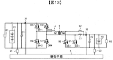
- FIG. 1 is an example of a circuit configuration diagram of a bidirectional DC-DC converter according to first to fourth embodiments of the present invention.
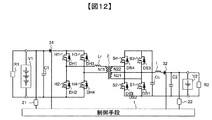
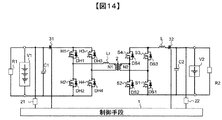
- 1 is an example of a circuit configuration diagram of a bidirectional DC-DC converter according to first to fourth embodiments of the present invention.
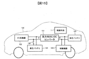
- FIG. 10 is a diagram showing a fifth embodiment using the bidirectional DC-DC converter of the present invention.
- FIG. 1 is a circuit configuration diagram of a bidirectional DC-DC converter according to Embodiment 1 of the present invention.
- the bidirectional DC-DC converter in the present embodiment is connected between the DC power supply V1 and the DC power supply V2, and transfers power between the DC power supply V1 and the DC power supply V2.
- a load R1 is connected in parallel to the DC power source V1, and a load R2 is connected in parallel to the DC power source V2.
- the smoothing capacitor C1 is connected in parallel to the DC power source V1
- the smoothing capacitor C2 is connected in parallel to the DC power source V2.
- the DC terminal of the first switching circuit is connected to the smoothing capacitor C1
- the DC terminal of the second switching circuit is connected to the smoothing capacitor C2.
- the primary winding N1 is connected to the AC terminal of the first switching circuit 11, and the secondary winding N2 is connected to the AC terminal of the second switching circuit 12.
- the transformer 2 magnetically couples the primary winding N1 and the secondary winding N2.
- the first switching circuit 11 and the second switching circuit 12 are controlled by the control means 1.
- a voltage sensor 21, a voltage sensor 22, a current sensor 31, and a current sensor 32 are connected to the control means 1.
- the voltage sensors 21 and 22 and the current sensors 31 and 32 may not be used.
- the control means 1 switches the first switching circuit 11 from the DC power source V1 and applies an AC voltage to the primary winding N1.
- the second switching circuit 12 rectifies the induced voltage generated in the secondary winding N2 and supplies power to the DC power supply V2.
- the control means 1 causes the second switching circuit 12 to perform a switching operation from the DC power source V2, and applies an AC voltage to the secondary winding N2.
- the first switching circuit 11 rectifies the induced voltage generated in the primary winding N1, and supplies power to the DC power supply V1.
- control means 1 increases the voltage of the primary winding N1 by supplying power from the DC power supply V1 before the second switching circuit 12 applies the AC voltage to the secondary winding N2 by the switching operation.
- the first switching circuit 11 is controlled so that
- the first switching circuit 11 is controlled by the first switching circuit 11 before the second switching circuit 12 applies the AC voltage to the secondary winding N2. Power is supplied to the circuit 11. Therefore, when the second switching circuit 12 applies an AC voltage to the secondary winding N2 by the switching operation, the power difference between the first switching circuit 11 and the second switching circuit 12 is reduced. Reverse power transmission from the DC power supply V2 to the DC power supply V1 is possible while suppressing a surge voltage generated in the second switching circuit 12 due to the power difference between the switching circuit 11 and the second switching circuit 12.
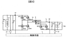
- FIG. 2 is a circuit configuration diagram of a bidirectional DC-DC converter according to Embodiment 2 of the present invention.
- the same reference numerals as those in the first embodiment have the same functions.
- Switching element H1 and switching element H2 are connected in series to form a first switching leg, and are connected to smoothing capacitor C1.
- Switching element H3 and switching element H4 are connected in series to form a second switching leg, and are connected to smoothing capacitor C1.
- the primary winding N11 and the resonant reactor Lr are connected in series between the series connection point of the switching element H1 and the switching element H2 and the series connection point of the switching element H3 and the switching element H4.
- the primary winding N11, the secondary winding N21, and the secondary winding N22 are magnetically coupled.
- One end of the secondary winding N21 and one end of the secondary winding N22 are connected.
- the other end of the secondary winding N21 is connected to one end of the switching element S1.
- the other end of the secondary winding N22 is connected to one end of the switching element S2.
- the other end of the switching element S1 and the other end of the switching element S2 are connected to one end of the smoothing capacitor C2.
- the connection point of the secondary windings N21 and N22 is connected to the other end of the smoothing capacitor C2 through the smoothing reactor L.
- the diodes DH1 to DH4, the diode DS1 and the diode DS2 are connected to the switching elements H1 to H4, the switching element S1 and the switching element S2, respectively.
- a MOSFET body diode can be used as the diode.
- the switching elements H1 to H4, S1, and S2 are controlled by the control means 1.
- a voltage sensor 21, a voltage sensor 22, a current sensor 31, and a current sensor 32 are connected to the control means 1. Note that it is not necessary to use all of the voltage sensor 21, the voltage sensor 22, and the current sensor 31 and the current sensor 32.
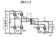
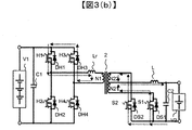
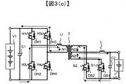
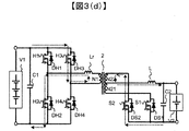
- FIGS. 3 (a) to 3 (d) are circuit diagrams illustrating the operation of the bidirectional DC-DC converter according to the second embodiment during forward power transmission.
- the operation during forward power transmission will be described in detail with reference to FIGS. 3 (a) to 3 (d).
- each of FIGS. 3 (a) to 3 (d) corresponds to modes a to d.
- Mode a As shown in FIG. 3 (a), in mode a, the switching elements H1 and H4 are in the on state, the switching elements H2 and H3 are in the off state, and the voltage of the DC power supply V1 is changed to the switching elements H1 and H4 and the resonant reactor. Applied to the primary winding N1 via Lr.
- the switching element S2 is in an off state, and the voltage generated in the secondary winding N2 is supplied with energy to the DC power supply V2 via the diode DS1 and the smoothing reactor L.
- the loss may be reduced by dividing the current flowing through the diode DS1 to the switching element S1.
- the reduction of the loss by turning on the MOSFET is hereinafter referred to as synchronous rectification.
- This mode d is a symmetrical operation of mode a.
- mode a is a symmetrical operation of mode a.
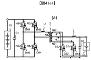
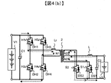
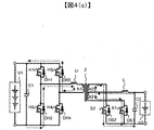
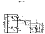
- FIGS. 4 (a) to 4 (e) are circuit diagrams illustrating an operation during reverse power transmission of the bidirectional DC-DC converter according to the second embodiment.
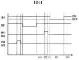
- FIG. 5 is a gate signal waveform diagram of the switching element during reverse power transmission of the bidirectional DC-DC converter according to the second embodiment.
- FIGS. 4 (a) to 4 (e) correspond to the periods (a) to (e) in FIG. 5, and correspond to the following modes a to e.
- Mode a As shown in FIG. 4 (a), in mode a, the switching elements S1 and S2 are turned on, and the voltage of the DC power supply V2 passes through the secondary windings N21 and N22 and the switching elements S1 and S2, and the smoothing reactor. Applied to L, the energy of the DC power source V2 is accumulated in the smoothing reactor L. Since the switching elements H1 to H4 are in the off state and the switching elements S1 and S2 are in the on state, no voltage is applied to the primary winding N1, and the current of the resonant reactor Lr is zero.
- Mode d As shown in FIG. 4D, when the switching element S1 is turned off, the voltage of the DC power source V2 is applied to the secondary winding N22, and the current increases in the resonant reactor Lr. Further, the energy accumulated in the smooth reactor L is released. At this time, because the current flows through the resonant reactor Lr in mode b, the amount of current that increases the current in the resonant reactor Lr in mode d is reduced, and applied to the switching element S1 when the switching element S1 is turned off. Surge voltage is reduced. Note that mode c and mode d may be the same period.
- the DC power source V2 energy is stored in the smoothing reactor L.
- This mode e is a symmetric operation of mode a. Thereafter, since the operation returns to mode a after symmetrical operation of modes b to e, it is assumed that it can be easily understood, and detailed description thereof is omitted.
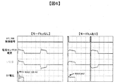
- Figure 6 shows the voltage and current waveforms during reverse transmission of the bidirectional DC-DC converter according to Example 2.
- the modes b and c are not provided.
- the energy of the smoothing reactor L is applied to the switching element S1 when the switching element S1 is turned off. A maximum of 188.4V) occurred.
- the current flows for the time width in which the switching reactors H1 and H4 are on in the resonant reactor Lr current in the mode d. Therefore, when the switching element S1 is turned off, the power of the smoothing reactor L is not applied to the switching element S1, and the power is supplied to the DC power supply V1, so the surge voltage can be suppressed (maximum 94V). It is.
- the present embodiment it is possible to suppress a surge voltage applied to the switching element during reverse power transmission of the bidirectional DC-DC converter and to provide a bidirectional DC-DC converter with high efficiency, small size, and low cost.
- Example 2 the voltage source full bridge circuit and the current source center tap circuit are combined, but the voltage source push-pull circuit, the current source center tap circuit with active clamp shown in FIG. 12 and other surge absorbing circuits, FIG. Naturally, the combination of the voltage source full bridge circuit and current doubler circuit shown in FIG. 14 and the combination of the voltage source full bridge circuit and current source full bridge circuit shown in FIG.
- FIG. 7 is a circuit configuration diagram of a bidirectional DC-DC converter according to Embodiment 3 of the present invention.
- the same reference numerals as those in the first embodiment have the same functions.
- the same reference numerals as those in the first embodiment have the same functions.
- the first switching leg in which the switching elements H1 and H2 are connected in series is connected to the smoothing capacitor C1 via the diode D0.
- the diode D0 is connected in such a direction as to send power from the first switching leg to the DC power supply V1 and not from the DC power supply V1 to the first switching leg, and a switch SW is connected in parallel to the diode D0.
- the second switching leg in which the switching elements H3 and H4 are connected in series is connected to the smoothing capacitor C1.
- the primary winding N1 and the resonant reactor Lr are connected in series between the series connection point of the switching elements H1 and H2 and the series connection point of the switching elements H3 and H4.
- Forward power transmission keeps the switch SW on. As a result, both ends of the diode D0 are short-circuited, so that the DC terminals of the first switching leg and the second switching leg are in the same state as when directly connected to the smoothing capacitor C1 without passing through the diode D0. .
- This state is the same as the circuit configuration of the second embodiment, and the switching operation is also the same. Therefore, since the operation at the time of forward transmission is the same as that of the second embodiment, the description is omitted.
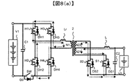
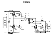
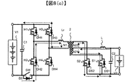
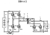
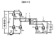
- FIG. 8A to FIG. 8F are circuit diagrams for explaining the operation at the time of reverse power transmission of the bidirectional DC-DC converter in the third embodiment.
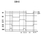
- FIG. 9 is a gate signal waveform diagram of the switching element during reverse power transmission of the bidirectional DC-DC converter according to the third embodiment.
- FIGS. 8 (a) to 8 (f) correspond to the periods (a) to (f), respectively, and represent the following modes a to f.
- Mode a As shown in FIG. 8 (a), in mode a, the switching elements S1 and S2 are turned on, and the voltage of the DC power supply V2 passes through the secondary windings N21 and N22 and the switching elements S1 and S2, and the smoothing reactor. Applied to L, the energy of the DC power source V2 is accumulated in the smoothing reactor L.
- the switching elements H1 and H4 are in the on state, the switching elements H2 and H3 are in the off state, and the current passing through the diodes DH2 and DH3, the switching elements H1, H4, and the primary winding N1 flows through the resonance reactor Lr. .
- MOSFETs are used as the switching elements H1 to H4
- synchronous rectification is achieved if the switching elements H2 and H3 are turned on.
- Mode d As shown in FIG. 8 (d), when the switching element S1 is turned off, the voltage of the DC power source V2 is applied to the secondary winding N22, and the current increases in the resonant reactor Lr. Further, the energy accumulated in the smooth reactor L is released. At this time, since the current flows through the resonant reactor Lr in mode b, the amount of current that increases the current in the resonant reactor Lr is reduced in mode d, so the switching element S1 when the switching element S1 is turned off is reduced. The applied surge voltage is reduced. Note that mode c and mode d may be the same period.
- the DC power source V2 energy is stored in the smoothing reactor L.
- the energy of DC power supply V2 is stored in smoothing reactor L.
- This mode f is a symmetrical operation of mode a.
- the operation returns to the mode a after the symmetrical operation of the modes b to f, it will be easily understood, and thus detailed description will be omitted.
- this embodiment allows reverse power transmission from the DC power supply V2 to the DC power supply V1 while suppressing the generation of the surge voltage of the switching elements S1, S2 as in Example 2.
- a synchronous rectification operation can be performed in modes a and f.
- the synchronous rectification operation in which the switching element is turned on can reduce conduction loss as compared with diode rectification, and can achieve higher efficiency of the bidirectional DC-DC converter.
- the present embodiment it is possible to suppress a surge voltage applied to the switching element during reverse power transmission of the bidirectional DC-DC converter and to provide a bidirectional DC-DC converter with high efficiency, small size, and low cost.
- Example 3 the voltage source full bridge circuit and the current source center tap circuit are combined, but the voltage source push-pull circuit, the current source center tap circuit with active clamp shown in FIG. 12 and other surge absorbing circuits, FIG. Naturally, the combination of the voltage source full bridge circuit and current doubler circuit shown in FIG. 14 and the combination of the voltage source full bridge circuit and current source full bridge circuit shown in FIG.
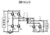
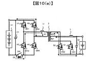
- FIGS. 10 (a) to 10 (g) are a circuit configuration diagram of a bidirectional DC-DC converter according to Embodiment 4 of the present invention and a circuit diagram illustrating an operation during reverse power transmission. Since the circuit configuration of the power conversion device according to the present embodiment is the same as that of Example 3, the description thereof is omitted.
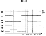
- FIG. 11 is a gate signal waveform diagram of the switching element during reverse power transmission of the bidirectional DC-DC converter according to the fourth embodiment.
- the operation at the time of reverse power transmission will be described in detail with reference to FIGS. 10 (a) to 10 (g) and FIG.
- FIGS. 10 (a) to 10 (g) correspond to the periods (a) to (g) in FIG. 11 and represent the following modes a to g. .
- Mode d As shown in FIG. 10 (d), when the switching element S1 is turned off, the voltage of the DC power source V2 is applied to the secondary winding N22, and the current increases in the resonant reactor Lr. Further, the energy accumulated in the smooth reactor L is released. At this time, since the current flows through the resonant reactor Lr in mode b, the amount of current that increases the current in the resonant reactor Lr is reduced in mode d, so the switching element S1 when the switching element S1 is turned off is reduced. The surge voltage applied to is reduced. Since the switch SW is on, current flows through the switch SW. When using a device such as IGBT that does not allow negative current to flow through the switch SW, current flows through the diode D0. Note that mode c and mode d may be the same period.
- This mode g is a symmetric operation of mode a.
- a detailed description is omitted.
- the present embodiment enables reverse power transmission from the DC power supply V2 to the DC power supply V1 while suppressing the occurrence of surge voltage of the switching elements S1, S2 as in Example 3, and a diode.
- D0 and the switch SW connected in parallel to the diode a synchronous rectification operation can be performed in modes a and f.
- the synchronous rectification operation in which the switching element is turned on can reduce conduction loss as compared with diode rectification, and can achieve higher efficiency of the bidirectional DC-DC converter.
- Embodiment 4 of the present invention can be realized by using an element capable of high-speed switching operation such as a MOSFET as the switching elements H1 to H4. is there. Therefore, the device options for the switch SW increase.
- Example 4 the voltage source full bridge circuit and the current source center tap circuit are combined, but the voltage source push-pull circuit, the current source center tap circuit with active clamp shown in FIG. 12 and other surge absorbing circuits, FIG. Naturally, the combination of the voltage source full bridge circuit and current doubler circuit shown in FIG. 14 and the combination of the voltage source full bridge circuit and current source full bridge circuit shown in FIG.
- FIG. 15 is a circuit configuration diagram of the bidirectional DC-DC converter according to the fifth embodiment of the present invention.
- the present embodiment relates to a method of using the bidirectional DC-DC converter in the first to fourth embodiments.
- the high-voltage side of the bidirectional DC-DC converter is the A side
- the low-voltage side is the B side.
- the circuit configuration is such that one end of the HV system device 102 such as a motor drive inverter is connected to one end on the A side of the bidirectional DC-DC converter 101, and the other end of the HV system device 102 is A of the bidirectional DC-DC converter 101. Is connected to the other end.
- One end of the high-voltage battery 104 is connected to one end on the A side of the bidirectional DC-DC converter 101, and the other end of the high-voltage battery 104 is connected to the other end on the A side of the bidirectional DC-DC converter 101 via the relay 106.
- One end of the low voltage battery 105 is connected to one end on the B side of the bidirectional DC-DC converter 101, and the other end of the low voltage battery 105 is connected to the other end on the B side of the bidirectional DC-DC converter 101.
- auxiliary equipment 103 such as an air conditioner is connected to one end on the B side of the bidirectional DC-DC converter, and the other end of the auxiliary equipment 103 is connected to the other end on the B side of the bidirectional DC-DC converter.
- the control means 1 controls the switching operation of the bidirectional DC-DC converter, the power transmission direction, the amount of power, and the like. Note that the relay may not be provided. In the fifth embodiment, there are the following forward power transmission operation and reverse power transmission operation.
- the high voltage battery 104 charges the low voltage battery 105 and supplies power to the auxiliary equipment 103 using a bidirectional DC-DC converter. Note that not only the high-voltage battery 104 but also power from the HV system device 102 may be used.
- the operation of the bidirectional DC-DC converter has a circuit configuration and a control configuration as in the second embodiment, for example.
- the low voltage battery 105 uses a bidirectional DC-DC converter to charge the high voltage battery 104 and supply power to the HV system device 102.
- the bidirectional DC-DC converter has a circuit configuration and a control configuration as in the second embodiment, for example.
- the bidirectional DC-DC converter Since the above-described forward power transmission operation and reverse power transmission operation by the bidirectional DC-DC converter enable bidirectional power conversion, the degree of freedom in designing the vehicle power supply system can be increased. Furthermore, by using the bidirectional DC-DC converter according to the present invention, the surge voltage applied to the switching element in the reverse power transmission operation is suppressed, and a bidirectional DC-DC converter with high efficiency, small size, and low cost can be provided. As a result, it becomes possible to achieve high efficiency, small size and low cost of automobiles.
- the present invention can be applied to all bidirectional DC-DC converters having an insulating function.
- SYMBOLS 1 Control means, 2 ... Transformer, 11 ... 1st switching circuit, 12 ... 2nd switching circuit, 21 ... Voltage sensor, 22 ... Voltage sensor, 31 ... Current sensor, 32 ... Current sensor, 100 ... Car, 101 ... Bidirectional DC-DC converter, 102 ... HV system, 103 ... Auxiliary equipment, 104 ... High voltage battery, 105 ... Low voltage battery, 106 ... Relay, C1 ... Smoothing capacitor, C2 ... Smoothing capacitor, L ... Smoothing reactor, Lr ... Resonant reactor, N1 ... Primary winding, N2 ... Secondary winding, N11 ... Primary winding, N21 ... Secondary winding, N22 ...
Landscapes
- Engineering & Computer Science (AREA)
- Power Engineering (AREA)
- Dc-Dc Converters (AREA)
Abstract
本発明の課題は、双方向DC-DCコンバータの昇圧動作時におけるサージ電圧を抑制し、高効率・小型・低コストな双方向DC-DCコンバータを実現できる回路および制御構成を提供することである。 本発明に係る電力変換装置は、降圧もしくは昇圧を行う電力変換装置DC-DCコンバータであって、1次巻線と2次巻線を磁気結合するトランスと、第1の電源及び前記1次巻線に対して電気的に並列に接続される第1スイッチング回路と、第2の電源及び前記2次巻線に対して電気的に並列に接続される第2スイッチング回路と、前記第1スイッチング回路及び前記第2スイッチング回路を制御する制御回路と、を備え、前記制御手段は前記トランスを介して前記第2の電源から前記第1の電源ヘ電力を送る前に、前記第1の電源から電力を供給して前記1次巻線の電圧を上昇させるように前記第1スイッチング回路を制御する。
Description
本発明は双方向DC-DCコンバータ、これを用いた電源システム及び当該電源システムを用いた自動車に関し、特に自動車に搭載される双方向DC-DCコンバータに関する。
近年、化石燃料の枯渇や地球環境問題の悪化を背景として、ハイブリッド自動車や電気自動車のような、電気エネルギーを利用した自動車への関心が高まっており、実用化されている。
このような電気エネルギーを用いた自動車は、車輪を駆動するためのモータに電力を供給するための高圧バッテリ電圧を降圧して、必要な電力を低圧の電気機器へ供給する電力変換装置が備えられることが多い。この低圧の電気機器の例として、エアコンやオーディオ、自動車のコントローラー等がある。低圧の電気機器に高圧バッテリから電力を供給する電力変換装置には、一般にDC-DCコンバータが用いられる。
また、DC-DCコンバータには降圧動作だけではなく、昇圧動作も可能である双方向DC-DCコンバータが求められている。これは高圧バッテリが放電してしまった場合に、低圧バッテリから電力を供給し、高圧バッテリを充電することで、高圧側機器を動作可能な状態にするために用いられている。このように電圧が異なるバッテリ間で電力を融通できれば、車両の電源システムの信頼性が向上し、また電源システムの設計自由度を増やすことができる。
そこで、電圧が異なる2つの電源間で双方向に電力を変換する双方向DC-DCコンバータが特開2002-165448号公報(特許文献1)に開示されている。このコンバータは、高圧側の回路と低圧側の回路とをトランスを介して接続している。高圧側回路のスイッチング素子を動作させることで、高圧側電源から低圧側電源へ電力を供給し、低圧側回路のスイッチング素子を動作させることで、低圧側電源から高圧側電源へ電力を供給する。昇圧動作時は、低圧側のスイッチング素子のON状態にすることで、低圧側バッテリのエネルギーを低圧側にある平滑リアクトルに蓄える期間と、低圧側のスイッチング素子のOFF状態にすることで、低圧側バッテリのエネルギーを高圧側へ送る期間を設けている。前述動作により、低圧側から高圧側へ電力が供給される。
しかし、高圧側にある共振リアクトルや、トランスの漏れインダクタンスにより、低圧側のスイッチング素子をOFF状態にした瞬間、平滑リアクトルに蓄積されたエネルギーが、共振リアクトルや、トランスの漏れインダクタンスにより、高圧側へ伝達されず、低圧側のスイッチング素子にエネルギーが印加されていた。この瞬間に低圧側のスイッチング素子の両端に大きなサージ電圧が発生していた。これにより、スイッチング素子の素子耐圧を増加させる必要があった。一般的に、素子耐圧が大きくなると素子のオン抵抗が大きくなるため、素子耐圧の増加は、DC-DCコンバータの素子数の増加、素子損失の増加によりDC-DCコンバータの高効率・小型・低コスト化の妨げとなっていた。
そこで、低圧側のスイッチング素子のサージ電圧を抑制する回路構成が特開2012-110108号公報(特許文献2)に開示されている。これは、低圧側のチョークリアクトルにサージ電圧抑制回路を追加することで、平滑リアクトルに起因するサージ電圧を低減している。前述回路により、サージ電圧を低減することで、低圧側のスイッチング素子に低耐圧の素子が使用可能となり、素子損失が低減されるため、高効率なDC-DCコンバータが提供される。
ところで、上述の特許文献2に記載の電力変換装置は、サージ電圧抑制回路が追加されるため、双方向DC-DCコンバータの小型・低コスト化の妨げとなってしまう問題があった。
本発明の目的は、大型化やコスト増大を抑制しながら高効率な双方向DC-DCコンバータおよびこれを備えた電源システムを提供することにある。
本発明に係る電力変換装置は、1次巻線と2次巻線を磁気結合するトランスと、第1の電源及び前記1次巻線に対して電気的に並列接続される第1のスイッチング回路と、第2の電源及び前記2次巻線に対して電気的に並列接続される第2のスイッチング回路と、前記第1のスイッチング回路及び前記第2スイッチング回路を制御する制御回路と、を備えた双方向DC-DCコンバータであって、前記制御手段は前記トランスを介して前記第2の電源から前記第1の電源ヘ電力を送る前に、前記第1の電源から電力を供給して前記1次巻線の電圧を上昇させるように前記第1のスイッチング回路を制御する。
本発明によれば、双方向DC-DCコンバータの昇圧動作時におけるスイッチング素子に印加されるサージ電圧を抑制し、大型化やコスト増大を抑制した高効率な双方向DC-DCコンバータを提供可能である。
以下、図面を参照して、本発明に係る電力変換装置の実施の形態について説明する。なお、直流電源V1から直流電源V2へ電力を伝送することを順送電と呼称し、直流電源V2から直流電源V1へ電力を伝送することを逆送電と呼称する。
各図において同一要素については同一の符号を記し、重複する説明は省略する。本発明は以下の実施形態に限定されることなく、本発明の技術的な概念の中で種々の変形例や応用例をもその範囲に含むものである。
(第1の実施形態)
(回路構成)
図1は、本発明の実施例1による双方向DC-DCコンバータの回路構成図である。本実施形態における双方向DC-DCコンバータは、直流電源V1と直流電源V2との間に接続され、直流電源V1と直流電源V2との間で電力の授受を行う。直流電源V1には負荷R1が並列接続され、直流電源V2には負荷R2が並列接続されている。
(回路構成)
図1は、本発明の実施例1による双方向DC-DCコンバータの回路構成図である。本実施形態における双方向DC-DCコンバータは、直流電源V1と直流電源V2との間に接続され、直流電源V1と直流電源V2との間で電力の授受を行う。直流電源V1には負荷R1が並列接続され、直流電源V2には負荷R2が並列接続されている。
図1において、平滑コンデンサC1は直流電源V1に並列接続され、平滑コンデンサC2は直流電源V2に並列接続されている。第1のスイッチング回路の直流端子は平滑コンデンサC1に接続され、第2のスイッチング回路の直流端子は平滑コンデンサC2に接続される。
第1のスイッチング回路11の交流端子には1次巻線N1が接続され、第2のスイッチング回路12の交流端子には2次巻線N2が接続されている。トランス2は、1次巻線N1と2次巻線N2とを磁気結合している。
第1のスイッチング回路11と、第2のスイッチング回路12は、制御手段1によって制御される。制御手段1には、電圧センサ21と電圧センサ22及び電流センサ31と電流センサ32が接続されている。なお、電圧センサ21、22および電流センサ31、32を用いなくてもよい。
(順送電)
実施例1による双方向DC-DCコンバータの順送電時の動作を説明する。制御手段1は、直流電源V1より、第1のスイッチング回路11をスイッチング動作させ、1次巻線N1に交流電圧を印加する。第2のスイッチング回路12は、2次巻線N2に生じた誘起電圧を整流し、直流電源V2に電力を供給する。
実施例1による双方向DC-DCコンバータの順送電時の動作を説明する。制御手段1は、直流電源V1より、第1のスイッチング回路11をスイッチング動作させ、1次巻線N1に交流電圧を印加する。第2のスイッチング回路12は、2次巻線N2に生じた誘起電圧を整流し、直流電源V2に電力を供給する。
(逆送電)
次に、実施例1における双方向DC-DCコンバータの逆送電時の動作を説明する。制御手段1は、直流電源V2より、第2のスイッチング回路12をスイッチング動作させ、2次巻線N2に交流電圧を印加する。第1のスイッチング回路11は、1次巻線N1に生じた誘起電圧を整流し、直流電源V1に電力を供給する。
次に、実施例1における双方向DC-DCコンバータの逆送電時の動作を説明する。制御手段1は、直流電源V2より、第2のスイッチング回路12をスイッチング動作させ、2次巻線N2に交流電圧を印加する。第1のスイッチング回路11は、1次巻線N1に生じた誘起電圧を整流し、直流電源V1に電力を供給する。
さらに、制御手段1は、第2のスイッチング回路12が、スイッチング動作により2次巻線N2に交流電圧を印加する前に、直流電源V1から電力を供給して1次巻線N1の電圧を上昇させるように第1のスイッチング回路11を制御する。
(本実施形態の効果)
このように、逆送電時は、第2のスイッチング回路12が2次巻線N2に交流電圧を印加する前に、第1のスイッチング回路11を制御することで、直流電源V1から第1のスイッチング回路11に電力を供給される。そのため、第2のスイッチング回路12が、スイッチング動作により2次巻線N2に交流電圧を印加した際に、第1のスイッチング回路11と第2のスイッチング回路12の電力差が低減さるため、第1のスイッチング回路11と第2のスイッチング回路12の電力差による第2のスイッチング回路12に発生するサージ電圧を抑制しながら、直流電源V2から直流電源V1への逆送電が可能である。
このように、逆送電時は、第2のスイッチング回路12が2次巻線N2に交流電圧を印加する前に、第1のスイッチング回路11を制御することで、直流電源V1から第1のスイッチング回路11に電力を供給される。そのため、第2のスイッチング回路12が、スイッチング動作により2次巻線N2に交流電圧を印加した際に、第1のスイッチング回路11と第2のスイッチング回路12の電力差が低減さるため、第1のスイッチング回路11と第2のスイッチング回路12の電力差による第2のスイッチング回路12に発生するサージ電圧を抑制しながら、直流電源V2から直流電源V1への逆送電が可能である。
本実施系形態によれば、双方向DC-DCコンバータの逆送電時におけるスイッチング回路に印加されるサージ電圧を抑制し、高効率・小型・低コストな双方向DC-DCコンバータを提供可能である。
(第2の実施形態)
(回路構成)
図2は、本発明の実施例2による双方向DC-DCコンバータの回路構成図である。第1の実施形態において付した符号と同一の符号は、同一の機能を有する。
(回路構成)
図2は、本発明の実施例2による双方向DC-DCコンバータの回路構成図である。第1の実施形態において付した符号と同一の符号は、同一の機能を有する。
スイッチング素子H1とスイッチング素子H2は、互いに直列接続されて第1のスイッチングレッグを構成し、平滑コンデンサC1に接続される。スイッチング素子H3、スイッチング素子H4は、互いに直列接続されて第2のスイッチングレッグを構成し、平滑コンデンサC1に接続される。
スイッチング素子H1とスイッチング素子H2の直列接続点と、スイッチング素子H3とスイッチング素子H4の直列接続点との間に、1次巻線N11と共振リアクトルLrとが直列接続されている。
トランス2は、1次巻線N11と2次巻線N21及び2次巻線N22とを磁気結合している。2次巻線N21の一端と2次巻線N22の一端とが接続される。2次巻線N21の他端はスイッチング素子S1の一端に接続される。2次巻線N22の他端はスイッチング素子S2の一端に接続される。スイッチング素子S1の他端とスイッチング素子S2の他端とが、平滑コンデンサC2の一端に接続される。2次巻線N21、N22の接続点は、平滑リアクトルLを介して平滑コンデンサC2の他端に接続される。
スイッチング素子H1ないしH4、スイッチング素子S1とスイッチング素子S2には、それぞれダイオードDH1ないしDH4、ダイオードDS1とダイオードDS2が接続されている。ここで、これらのスイッチング素子として、Si-MOSFETやSiC-MOSFETを使用した場合は、ダイオードとしてMOSFETのボディダイオードを利用することができる。
スイッチング素子H1ないしH4、S1、S2は、制御手段1によって制御される。制御手段1には、電圧センサ21と電圧センサ22及び電流センサ31と電流センサ32が接続されている。なお、電圧センサ21と電圧センサ22およぶ電流センサ31と電流センサ32をすべて用いなくてもよい。
(順送電)
図3(a)ないし 図3 (d)は、実施例2における双方向DC-DCコンバータの順送電時の動作を説明する回路図である。以下、この図3(a)ないし 図3 (d)を参照しながら順送電時の動作を詳細に説明する。だだし、図3において、図3 (a)ないし 図3 (d)のそれぞれはモードa~dに対応する。
図3(a)ないし 図3 (d)は、実施例2における双方向DC-DCコンバータの順送電時の動作を説明する回路図である。以下、この図3(a)ないし 図3 (d)を参照しながら順送電時の動作を詳細に説明する。だだし、図3において、図3 (a)ないし 図3 (d)のそれぞれはモードa~dに対応する。
(モードa)
図3 (a)に示されるように、モードaでは、スイッチング素子H1、H4がオン状態、スイッチング素子H2、H3がオフ状態であり、直流電源V1の電圧が、スイッチング素子H1、H4、共振リアクトルLrを介して1次巻線N1に印加されている。
図3 (a)に示されるように、モードaでは、スイッチング素子H1、H4がオン状態、スイッチング素子H2、H3がオフ状態であり、直流電源V1の電圧が、スイッチング素子H1、H4、共振リアクトルLrを介して1次巻線N1に印加されている。
スイッチング素子S2はオフ状態であり、2次巻線N2に生じた電圧が、ダイオードDS1、平滑リアクトルLを介して、直流電源V2にエネルギーが供給される。
この時、スイッチング素子S1、S2として、MOSFETを用いる場合は、スイッチング素子S1をオン状態とすれば、ダイオードDS1に流れる電流をスイッチング素子S1へ分流することで損失を低減できる場合がある。このように、MOSFETと逆並列接続されたダイオード、またはMOSFETのボディダイオードに、ダイオードの順方向電流が流れるとき、このMOSFETをオン状態として損失を低減することを、以後同期整流と呼称する。
(モードb)
図3 (b)に示されるように、スイッチング素子H4をオフすると、スイッチング素子H4を流れていた電流は、ダイオードDH3、スイッチング素子H1、共振リアクトルLr、1次巻線N1へ流れる。この時、スイッチング素子H3をオンさせる。
図3 (b)に示されるように、スイッチング素子H4をオフすると、スイッチング素子H4を流れていた電流は、ダイオードDH3、スイッチング素子H1、共振リアクトルLr、1次巻線N1へ流れる。この時、スイッチング素子H3をオンさせる。
このとき、2次巻線N21に流れていた電流は減少し、2次巻線N22に流れる電流が、ダイオードDS2を介して流れる。この時にスイッチング素子S2をオンすれば同期整流となる。平滑リアクトルLに蓄えられたエネルギーは直流電源V2に供給される。
(モードc)
図3 (c)に示されるように、スイッチング素子H1がオフすると、スイッチング素子H1を流れていた電流は、直流電源V1、ダイオードDH2、共振リアクトルLr、1次巻線N1、スイッチング素子H3またはダイオードDH3へ流れる。この時、スイッチング素子H2をオンすれば同期整流となる。共振リアクトルLrには、直流電源V1の電圧が印加され、この電流は減少していく。
図3 (c)に示されるように、スイッチング素子H1がオフすると、スイッチング素子H1を流れていた電流は、直流電源V1、ダイオードDH2、共振リアクトルLr、1次巻線N1、スイッチング素子H3またはダイオードDH3へ流れる。この時、スイッチング素子H2をオンすれば同期整流となる。共振リアクトルLrには、直流電源V1の電圧が印加され、この電流は減少していく。
(モードd)
図3 (d)に示されるように、スイッチング素子H2、H3がオン状態であるから、共振リアクトルLrの電流がゼロに達した後は、逆向きにこの電流が増加していく。これに伴い、ダイオードDS1またはスイッチング素子S1と2次巻線N21に流れる電流は減少し、ダイオードDS2またはスイッチング素子S2と2次巻線N22に流れる電流は増加していく。2次巻線N21に流れる電流がゼロになる前に、スイッチング素子S1をオフ状態にする。
図3 (d)に示されるように、スイッチング素子H2、H3がオン状態であるから、共振リアクトルLrの電流がゼロに達した後は、逆向きにこの電流が増加していく。これに伴い、ダイオードDS1またはスイッチング素子S1と2次巻線N21に流れる電流は減少し、ダイオードDS2またはスイッチング素子S2と2次巻線N22に流れる電流は増加していく。2次巻線N21に流れる電流がゼロになる前に、スイッチング素子S1をオフ状態にする。
このモードdはモードaの対称動作である。以降、モードb~dの対称動作の後、モードaに戻るため容易に理解できると考えるので、詳細な説明は省略する。
(逆送電)
図4(a)ないし図4(e)は、実施例2における双方向DC-DCコンバータの逆送電時の動作を説明する回路図である。また、図5は実施例2による双方向DC-DCコンバータの逆送電時のスイッチング素子のゲート信号波形図である。以下、この図4(a)ないし図4(e)、図5を参照しながら逆送電時の動作を詳細に説明する。だだし、図4において、(a)~(e)は図5の(a)~(e)の期間に対応しており、以下のモードa~eに対応する。
図4(a)ないし図4(e)は、実施例2における双方向DC-DCコンバータの逆送電時の動作を説明する回路図である。また、図5は実施例2による双方向DC-DCコンバータの逆送電時のスイッチング素子のゲート信号波形図である。以下、この図4(a)ないし図4(e)、図5を参照しながら逆送電時の動作を詳細に説明する。だだし、図4において、(a)~(e)は図5の(a)~(e)の期間に対応しており、以下のモードa~eに対応する。
(モードa)
図4 (a)に示されるように、モードaでは、スイッチング素子S1、S2がオン状態、直流電源V2の電圧が、2次巻線N21、N22、スイッチング素子S1、S2を介して、平滑リアクトルLに印加され、直流電源V2のエネルギーを平滑リアクトルLに蓄積している。スイッチング素子H1~ H4はオフ状態であり、スイッチング素子S1、S2がオン状態であるため、1次巻線N1に電圧が印加されず、共振リアクトルLrの電流はゼロである。
図4 (a)に示されるように、モードaでは、スイッチング素子S1、S2がオン状態、直流電源V2の電圧が、2次巻線N21、N22、スイッチング素子S1、S2を介して、平滑リアクトルLに印加され、直流電源V2のエネルギーを平滑リアクトルLに蓄積している。スイッチング素子H1~ H4はオフ状態であり、スイッチング素子S1、S2がオン状態であるため、1次巻線N1に電圧が印加されず、共振リアクトルLrの電流はゼロである。
(モードb)
図4 (b)に示されるように、スイッチング素子H1、H4をオンすると、スイッチング素子H4、直流電源V1、スイッチング素子H1を介して、共振リアクトルLrと1次巻線N1に電流が流れる。この時、2次巻線N21、N22にはそれぞれ逆向きに直流電源V2が印加されるため、1次巻線N1の電圧はゼロである。そのため、直流電源V1の電圧は、共振リアクトルLrに印加される。
図4 (b)に示されるように、スイッチング素子H1、H4をオンすると、スイッチング素子H4、直流電源V1、スイッチング素子H1を介して、共振リアクトルLrと1次巻線N1に電流が流れる。この時、2次巻線N21、N22にはそれぞれ逆向きに直流電源V2が印加されるため、1次巻線N1の電圧はゼロである。そのため、直流電源V1の電圧は、共振リアクトルLrに印加される。
(モードc)
図4 (c)に示されるように、スイッチング素子H1、H4をオフすると、共振リアクトルLrは電流を流し続けるため、ダイオードDH3、直流電源V1、ダイオードDH2を介して、共振リアクトルLrに電流が流れる。
図4 (c)に示されるように、スイッチング素子H1、H4をオフすると、共振リアクトルLrは電流を流し続けるため、ダイオードDH3、直流電源V1、ダイオードDH2を介して、共振リアクトルLrに電流が流れる。
(モードd)
図4 (d)に示されるように、スイッチング素子S1をオフすると、2次巻線N22に直流電源V2の電圧が印加され、共振リアクトルLrに電流が増加していく。また、平滑リアクトルLに蓄積されたエネルギーは放出されていく。この時、モードbにより、共振リアクトルLrに電流が流れているため、モードdで共振リアクトルのLrの電流を増加させる電流量が軽減され、スイッチング素子S1をオフする際の、スイッチング素子S1に印加されるサージ電圧が軽減される。なお、モードcとモードdは同一期間でもよい。
図4 (d)に示されるように、スイッチング素子S1をオフすると、2次巻線N22に直流電源V2の電圧が印加され、共振リアクトルLrに電流が増加していく。また、平滑リアクトルLに蓄積されたエネルギーは放出されていく。この時、モードbにより、共振リアクトルLrに電流が流れているため、モードdで共振リアクトルのLrの電流を増加させる電流量が軽減され、スイッチング素子S1をオフする際の、スイッチング素子S1に印加されるサージ電圧が軽減される。なお、モードcとモードdは同一期間でもよい。
(モードe)
図4 (e)に示されるように、スイッチング素子S1をオンすると、2次巻線N21、N22に直流電源V2の電圧がそれぞれ逆向きに印加されるため、1次巻線N1に印加される電圧が生じなくなり、共振リアクトルLrの電流は減少していき、やがてゼロとなる。
図4 (e)に示されるように、スイッチング素子S1をオンすると、2次巻線N21、N22に直流電源V2の電圧がそれぞれ逆向きに印加されるため、1次巻線N1に印加される電圧が生じなくなり、共振リアクトルLrの電流は減少していき、やがてゼロとなる。
また、モードaと同様に、直流電源V2のエネルギーを平滑リアクトルLに蓄積している。
このモードeはモードaの対称動作である。以降、モードb~eの対称動作の後、モードaに戻るため、容易に理解できると考え、詳細な説明は省略する。
(実施例の効果)
以上、説明したように、逆送電時は、スイッチング素子H1、H4をオンすると、スイッチング素子H4、直流電源V1、スイッチング素子H1を介して、共振リアクトルLrと1次巻線N1に電流が流れる。この時、2次巻線N21、N22にはそれぞれ逆向きに直流電源V2が印加されるため、1次巻線N1の電圧はゼロである。そのため、直流電源V1の電圧は、共振リアクトルLrに印加される。
以上、説明したように、逆送電時は、スイッチング素子H1、H4をオンすると、スイッチング素子H4、直流電源V1、スイッチング素子H1を介して、共振リアクトルLrと1次巻線N1に電流が流れる。この時、2次巻線N21、N22にはそれぞれ逆向きに直流電源V2が印加されるため、1次巻線N1の電圧はゼロである。そのため、直流電源V1の電圧は、共振リアクトルLrに印加される。
さらにスイッチング素子S1をオフすると、2次巻線N22に直流電源V2の電圧が印加され、共振リアクトルLrに電流が増加していく。スイッチング素子S1をオフする際に、共振リアクトルLrに電流を流しているため、共振リアクトルLrにエネルギーが蓄積されるため、スイッチング素子S1をオフした際、平滑リアクトルLのエネルギーが、スイッチング素子S1に印加されることなく、直流電源V1へ電力が供給される。スイッチング素子S2についても同様である。
よって、スイッチング素子S1、S2のサージ電圧の発生を抑制しながら、直流電源V2から直流電源V1への逆送電が可能である。
図6に実施例2による双方向DC-DCコンバータの逆送電時の電圧・電流波形図を示す。説明のため、モードb、cを設けない場合も記載している。モードb、cを設けない場合、モードdで共振リアクトルLr電流がゼロであるため、スイッチング素子S1をオフした際、平滑リアクトルLのエネルギーが、スイッチング素子S1に印加されるため、大きなサージ電圧(最大188.4V)が発生していた。
一方、本実施形態のようにモードb、cを設けた場合、モードdで共振リアクトルLr電流がスイッチングH1、H4がオンしていた時間幅分、電流が流れている。そのため、スイッチング素子S1をオフした際、平滑リアクトルLのエネルギーが、スイッチング素子S1に印加されることなく、直流電源V1へ電力が供給されるため、サージ電圧を抑制(最大94V)することが可能である。
本実施形態によれば、双方向DC-DCコンバータの逆送電時におけるスイッチング素子に印加されるサージ電圧を抑制し、高効率・小型・低コストな双方向DC-DCコンバータを提供可能である。
また、実施例2では、電圧形フルブリッジ回路と電流形センタタップ回路の組合せとしたが、電圧形プッシュプル回路、図12に示すアクティブクランプ付き電流形センタタップ回路やその他サージ吸収回路、図13に示す電圧形フルブリッジ回路とカレントダブラ回路、図14に示す電圧形フルブリッジ回路と電流形フルブリッジ回路の組合せでも同様の構成、制御、効果を有することは当然である。
(第3の実施形態)
(回路構成)
図7は、本発明の実施例3による双方向DC-DCコンバータの回路構成図である。第1の実施形態において付した符号と同一の符号は、同一の機能を有する。第1の実施形態において付した符号と同一の符号は、同一の機能を有する。
(回路構成)
図7は、本発明の実施例3による双方向DC-DCコンバータの回路構成図である。第1の実施形態において付した符号と同一の符号は、同一の機能を有する。第1の実施形態において付した符号と同一の符号は、同一の機能を有する。
スイッチング素子H1、H2を直列接続した第1のスイッチングレッグは、ダイオードD0を介して平滑コンデンサC1に接続される。このダイオードD0は、第1のスイッチングレッグから直流電源V1へは電力を送り、直流電源V1から第1のスイッチングレッグへ送らない向きに接続され、ダイオードD0にはスイッチSWが並列接続されている。スイッチング素子H3、H4を直列接続した第2のスイッチングレッグは平滑コンデンサC1に接続される。スイッチング素子H1、H2の直列接続点と、スイッチング素子H3、H4の直列接続点との間に、1次巻線N1、共振リアクトルLrとが直列接続されている。
その他構成は、図4、7より実施例2と同様であるため、省略する。
(順送電)
順送電は、スイッチSWをオン状態に保つ。これにより、ダイオードD0の両端は短絡されるため、第1のスイッチングレッグおよび第2のスイッチングレッグの直流端子は、ダイオードD0を介さず、直接平滑コンデンサC1に接続された場合と同様の状態となる。この状態は、実施例2の回路構成と同様であり、スイッチング動作も同様である。よって、順伝送時の動作は実施例2と同様であるため省略する。
順送電は、スイッチSWをオン状態に保つ。これにより、ダイオードD0の両端は短絡されるため、第1のスイッチングレッグおよび第2のスイッチングレッグの直流端子は、ダイオードD0を介さず、直接平滑コンデンサC1に接続された場合と同様の状態となる。この状態は、実施例2の回路構成と同様であり、スイッチング動作も同様である。よって、順伝送時の動作は実施例2と同様であるため省略する。
(逆送電)
図8(a)ないし 図8 (f)は、実施例3における双方向DC-DCコンバータの逆送電時の動作を説明する回路図である。また、図9は実施例3による双方向DC-DCコンバータの逆送電時のスイッチング素子のゲート信号波形図である。以下、この図8(a)ないし 図8 (f)、図9を参照しながら逆送電時の動作を詳細に説明する。だだし、図8(a)ないし 図8 (f)において、それぞれ(a)~(f)の期間に対応しており、以下のモードa~fを表す。
図8(a)ないし 図8 (f)は、実施例3における双方向DC-DCコンバータの逆送電時の動作を説明する回路図である。また、図9は実施例3による双方向DC-DCコンバータの逆送電時のスイッチング素子のゲート信号波形図である。以下、この図8(a)ないし 図8 (f)、図9を参照しながら逆送電時の動作を詳細に説明する。だだし、図8(a)ないし 図8 (f)において、それぞれ(a)~(f)の期間に対応しており、以下のモードa~fを表す。
(モードa)
図8(a)に示されるように、モードaでは、スイッチング素子S1、S2がオン状態、直流電源V2の電圧が、2次巻線N21、N22、スイッチング素子S1、S2を介して、平滑リアクトルLに印加され、直流電源V2のエネルギーを平滑リアクトルLに蓄積している。スイッチング素子H1、H4がオン状態、スイッチング素子H2、H3がオフ状態であり、共振リアクトルLrには、ダイオードDH2、DH3と、スイッチング素子H1、H4、1次巻線N1を通る電流が流れている。この時、スイッチング素子H1~H4としてMOSFETを用いている場合は、スイッチング素子H2、H3をオン状態にすれば同期整流である。
図8(a)に示されるように、モードaでは、スイッチング素子S1、S2がオン状態、直流電源V2の電圧が、2次巻線N21、N22、スイッチング素子S1、S2を介して、平滑リアクトルLに印加され、直流電源V2のエネルギーを平滑リアクトルLに蓄積している。スイッチング素子H1、H4がオン状態、スイッチング素子H2、H3がオフ状態であり、共振リアクトルLrには、ダイオードDH2、DH3と、スイッチング素子H1、H4、1次巻線N1を通る電流が流れている。この時、スイッチング素子H1~H4としてMOSFETを用いている場合は、スイッチング素子H2、H3をオン状態にすれば同期整流である。
(モードb)
図8(b)に示されるように、スイッチング素子H1、H4、スイッチSWをオンすると、スイッチング素子H4、スイッチSW、直流電源V1、スイッチング素子H1を介して、共振リアクトルLrと1次巻線N1に電流が流れる。この時、2次巻線N21、N22にはそれぞれ逆向きに直流電源V2が印加されるため、1次巻線N1の電圧はゼロである。そのため、直流電源V1の電圧は、共振リアクトルLrに印加される。
図8(b)に示されるように、スイッチング素子H1、H4、スイッチSWをオンすると、スイッチング素子H4、スイッチSW、直流電源V1、スイッチング素子H1を介して、共振リアクトルLrと1次巻線N1に電流が流れる。この時、2次巻線N21、N22にはそれぞれ逆向きに直流電源V2が印加されるため、1次巻線N1の電圧はゼロである。そのため、直流電源V1の電圧は、共振リアクトルLrに印加される。
(モードc)
図8(c)に示されるように、スイッチング素子H1、H4、スイッチSWをオフすると、共振リアクトルLrは電流を流し続けるため、ダイオードDH3、直流電源V1、ダイオードD0、ダイオードDH2を介して、共振リアクトルLrに電流が流れる。
図8(c)に示されるように、スイッチング素子H1、H4、スイッチSWをオフすると、共振リアクトルLrは電流を流し続けるため、ダイオードDH3、直流電源V1、ダイオードD0、ダイオードDH2を介して、共振リアクトルLrに電流が流れる。
(モードd)
図8(d)に示されるように、スイッチング素子S1をオフすると、2次巻線N22に直流電源V2の電圧が印加され、共振リアクトルLrに電流が増加していく。また、平滑リアクトルLに蓄積されたエネルギーは放出されていく。この時、モードbにより、共振リアクトルLrに電流が流れているため、モードdで共振リアクトルLrの電流を増加させる電流量が軽減されるため、スイッチング素子S1をオフする際の、スイッチング素子S1に印加されるサージ電圧が軽減される。なお、モードcとモードdは同一期間でもよい。
図8(d)に示されるように、スイッチング素子S1をオフすると、2次巻線N22に直流電源V2の電圧が印加され、共振リアクトルLrに電流が増加していく。また、平滑リアクトルLに蓄積されたエネルギーは放出されていく。この時、モードbにより、共振リアクトルLrに電流が流れているため、モードdで共振リアクトルLrの電流を増加させる電流量が軽減されるため、スイッチング素子S1をオフする際の、スイッチング素子S1に印加されるサージ電圧が軽減される。なお、モードcとモードdは同一期間でもよい。
(モードe)
図8(e)に示されるように、スイッチング素子S1をオンすると、2次巻線N21、N22に直流電源V2の電圧がそれぞれ逆向きに印加されるため、1次巻線N1に印加される電圧が生じない。スイッチング素子H2、H3がオン状態、スイッチSWがオフ状態なので、共振リアクトルLrには、直流電源V1の電圧が印加されるため、共振リアクトルLrの電流は減少していく。共振リアクトルLrの電流がゼロになると、ダイオードD0が逆導通し、共振リアクトルLrには、モードdとは逆向きの電流が流れる。
図8(e)に示されるように、スイッチング素子S1をオンすると、2次巻線N21、N22に直流電源V2の電圧がそれぞれ逆向きに印加されるため、1次巻線N1に印加される電圧が生じない。スイッチング素子H2、H3がオン状態、スイッチSWがオフ状態なので、共振リアクトルLrには、直流電源V1の電圧が印加されるため、共振リアクトルLrの電流は減少していく。共振リアクトルLrの電流がゼロになると、ダイオードD0が逆導通し、共振リアクトルLrには、モードdとは逆向きの電流が流れる。
また、モードaと同様に、直流電源V2のエネルギーを平滑リアクトルLに蓄積している。
(モードf)
図8(f)に示されるように、ダイオードD0が逆回復すると、このダイオードD0の導通中に蓄積された共振リアクトルLrの電流は、ダイオードDH1、DH4を導通し、ダイオードDH1、DH4、1次巻線N1、スイッチング素子H2、H3を流れる。この時、スイッチング素子H1~H4としてMOSFETを用いている場合は、スイッチング素子H1、H4をオン状態にすれば同期整流である。
図8(f)に示されるように、ダイオードD0が逆回復すると、このダイオードD0の導通中に蓄積された共振リアクトルLrの電流は、ダイオードDH1、DH4を導通し、ダイオードDH1、DH4、1次巻線N1、スイッチング素子H2、H3を流れる。この時、スイッチング素子H1~H4としてMOSFETを用いている場合は、スイッチング素子H1、H4をオン状態にすれば同期整流である。
また、モードa、eと同様に、直流電源V2のエネルギーを平滑リアクトルLに蓄積している。
このモードfはモードaの対称動作である。以降、モードb~fの対称動作の後、モードaに戻るため容易に理解できると考えるので、詳細な説明は省略する。
(実施例の効果)
以上、説明したように、本実施形態は、実施例2と同様にスイッチング素子S1、S2のサージ電圧の発生を抑制しながら、直流電源V2から直流電源V1への逆送電が可能であるとともに、ダイオードD0と、ダイオードに並列接続されたスイッチSWを用いることで、モードa、fにおいて同期整流動作が可能となる。スイッチング素子をオン状態にする同期整流動作は、ダイオード整流に比べ導通損失を低減することが可能であり、双方向DC-DCコンバータのさらなる高効率化を実現できる。
以上、説明したように、本実施形態は、実施例2と同様にスイッチング素子S1、S2のサージ電圧の発生を抑制しながら、直流電源V2から直流電源V1への逆送電が可能であるとともに、ダイオードD0と、ダイオードに並列接続されたスイッチSWを用いることで、モードa、fにおいて同期整流動作が可能となる。スイッチング素子をオン状態にする同期整流動作は、ダイオード整流に比べ導通損失を低減することが可能であり、双方向DC-DCコンバータのさらなる高効率化を実現できる。
本実施形態によれば、双方向DC-DCコンバータの逆送電時におけるスイッチング素子に印加されるサージ電圧を抑制し、高効率・小型・低コストな双方向DC-DCコンバータを提供可能である。
また、実施例3では、電圧形フルブリッジ回路と電流形センタタップ回路の組合せとしたが、電圧形プッシュプル回路、図12に示すアクティブクランプ付き電流形センタタップ回路やその他サージ吸収回路、図13に示す電圧形フルブリッジ回路とカレントダブラ回路、図14に示す電圧形フルブリッジ回路と電流形フルブリッジ回路の組合せでも同様の構成、制御、効果を有することは当然である。
(第4の実施形態)
(回路構成)
図10(a)ないし図10(g)は、本発明の実施例4による双方向DC-DCコンバータの回路構成図及び逆送電時の動作を説明する回路図である。本実施形態における電力変換装置は、回路構成は実施例3と同様であるため省略する。
(回路構成)
図10(a)ないし図10(g)は、本発明の実施例4による双方向DC-DCコンバータの回路構成図及び逆送電時の動作を説明する回路図である。本実施形態における電力変換装置は、回路構成は実施例3と同様であるため省略する。
(順送電)
順送電動作は、実施例3と同様であるため省略する。
順送電動作は、実施例3と同様であるため省略する。
(逆送電)
図11は実施例4による双方向DC-DCコンバータの逆送電時のスイッチング素子のゲート信号波形図である。以下、この図10(a)ないし図10(g)と図11を参照しながら逆送電時の動作を詳細に説明する。だだし、図10(a)ないし図10(g)において、(a)~(g)は図11の(a)~(g)の期間に対応しており、以下のモードa~gを表す。
図11は実施例4による双方向DC-DCコンバータの逆送電時のスイッチング素子のゲート信号波形図である。以下、この図10(a)ないし図10(g)と図11を参照しながら逆送電時の動作を詳細に説明する。だだし、図10(a)ないし図10(g)において、(a)~(g)は図11の(a)~(g)の期間に対応しており、以下のモードa~gを表す。
(モードa)
図10(a)に示されるモードaは実施例3のモードaと同様であるため省略する。
図10(a)に示されるモードaは実施例3のモードaと同様であるため省略する。
(モードb)
図10(b)に示されるモードbは実施例3のモードbと同様であるため省略する。
図10(b)に示されるモードbは実施例3のモードbと同様であるため省略する。
(モードc)
図10(c)に示されるように、スイッチング素子H1、H4をオフすると、共振リアクトルLrは電流を流し続けるため、ダイオードDH3、直流電源V1、スイッチSW、ダイオードDH2を介して、共振リアクトルLrに電流が流れる。
図10(c)に示されるように、スイッチング素子H1、H4をオフすると、共振リアクトルLrは電流を流し続けるため、ダイオードDH3、直流電源V1、スイッチSW、ダイオードDH2を介して、共振リアクトルLrに電流が流れる。
(モードd)
図10(d)に示されるように、スイッチング素子S1をオフすると、2次巻線N22に直流電源V2の電圧が印加され、共振リアクトルLrに電流が増加していく。また、平滑リアクトルLに蓄積されたエネルギーは放出されていく。この時、モードbにより、共振リアクトルLrに電流を流しているため、モードdで共振リアクトルのLrの電流を増加させる電流量が軽減されるため、スイッチング素子S1をオフする際の、スイッチング素子S1に印加されるサージ電圧が軽減される。スイッチSWがオン状態なので、電流はスイッチSWを流れる。スイッチSW にIGBTなど負方向電流が流せないデバイスを使用する場合は、電流はダイオードD0を流れる。なお、モードcとモードdは同一期間でもよい。
図10(d)に示されるように、スイッチング素子S1をオフすると、2次巻線N22に直流電源V2の電圧が印加され、共振リアクトルLrに電流が増加していく。また、平滑リアクトルLに蓄積されたエネルギーは放出されていく。この時、モードbにより、共振リアクトルLrに電流を流しているため、モードdで共振リアクトルのLrの電流を増加させる電流量が軽減されるため、スイッチング素子S1をオフする際の、スイッチング素子S1に印加されるサージ電圧が軽減される。スイッチSWがオン状態なので、電流はスイッチSWを流れる。スイッチSW にIGBTなど負方向電流が流せないデバイスを使用する場合は、電流はダイオードD0を流れる。なお、モードcとモードdは同一期間でもよい。
(モードe)
図10(e)に示されるように、スイッチSWをオフすると、スイッチSWを流れていた電流はダイオードD0に転流する。
図10(e)に示されるように、スイッチSWをオフすると、スイッチSWを流れていた電流はダイオードD0に転流する。
(モードf)
図10(f)に示されるモードfは実施例3のモードeと同様であるため省略する。
図10(f)に示されるモードfは実施例3のモードeと同様であるため省略する。
(モードg)
図10(g)に示されるモードgは実施例3のモードfと同様であるため省略する。
図10(g)に示されるモードgは実施例3のモードfと同様であるため省略する。
このモードgはモードaの対称動作である。以降、モードb~gの対称動作の後、モードaに戻るため容易に理解できると考えるので、詳細な説明は省略する。
(実施例の効果)
以上、説明したように、本実施形態は実施例3と同様にスイッチング素子S1、S2のサージ電圧の発生を抑制しながら、直流電源V2から直流電源V1への逆送電が可能であるとともに、ダイオードD0と、ダイオードに並列接続されたスイッチSWを用いることで、モードa、fにおいて同期整流動作が可能となる。スイッチング素子をオン状態にする同期整流動作は、ダイオード整流に比べ導通損失を低減することが可能であり、双方向DC-DCコンバータのさらなる高効率化を実現できる。さらに、スイッチSWが、IGBTなどオンオフ動作の遅い素子を使用した場合でも、スイッチング素子H1~H4をMOSFETなど高速スイッチング動作が可能な素子を使用することで、本発明の実施例4を実現可能である。よって、スイッチSWのデバイス選択肢が増大する。
以上、説明したように、本実施形態は実施例3と同様にスイッチング素子S1、S2のサージ電圧の発生を抑制しながら、直流電源V2から直流電源V1への逆送電が可能であるとともに、ダイオードD0と、ダイオードに並列接続されたスイッチSWを用いることで、モードa、fにおいて同期整流動作が可能となる。スイッチング素子をオン状態にする同期整流動作は、ダイオード整流に比べ導通損失を低減することが可能であり、双方向DC-DCコンバータのさらなる高効率化を実現できる。さらに、スイッチSWが、IGBTなどオンオフ動作の遅い素子を使用した場合でも、スイッチング素子H1~H4をMOSFETなど高速スイッチング動作が可能な素子を使用することで、本発明の実施例4を実現可能である。よって、スイッチSWのデバイス選択肢が増大する。
本実施形態によれば、双方向DC-DCコンバータの逆送電時におけるサージ電圧を抑制し、高効率・小型・低コストな双方向DC-DCコンバータを提供することが可能である。
また、実施例4では、電圧形フルブリッジ回路と電流形センタタップ回路の組合せとしたが、電圧形プッシュプル回路、図12に示すアクティブクランプ付き電流形センタタップ回路やその他サージ吸収回路、図13に示す電圧形フルブリッジ回路とカレントダブラ回路、図14に示す電圧形フルブリッジ回路と電流形フルブリッジ回路の組合せでも同様の構成、制御、効果を有することは当然である。
(第5の実施形態)
(回路構成)
図15は、本発明の実施例5による双方向DC-DCコンバータの回路構成図である。本実施例は、実施例1から実施4における双方向DC-DCコンバータの使用方法に関するものである。なお、双方向DC-DCコンバータの高圧側をA側、低圧側をB側とする。回路構成は、モータ駆動用インバータなどのHV系機器102の一端が双方向DC-DCコンバータ101のA側の一端に接続され、HV系機器102の他端が双方向DC-DCコンバータ101のA側の他端に接続される。高圧バッテリ104の一端は、双方向DC-DCコンバータ101のA側の一端に接続され、高圧バッテリ104の他端は、リレー106を介して、双方向DC-DCコンバータ101のA側の他端に接続される。低圧バッテリ105の一端は、双方向DC-DCコンバータ101のB側の一端に接続され、低圧バッテリ105の他端は、双方向DC-DCコンバータ101のB側の他端に接続される。エアコンなどの補機機器103の一端は双方向DC-DCコンバータのB側の一端に接続され、補機機器103の他端は双方向DC-DCコンバータのB側の他端に接続されている。制御手段1は、双方向DC-DCコンバータのスイッチング動作や、電力の送電方向、電力量などを制御している。なお、リレーはなくてもよい。
第5の実施形態において、以下の順送電動作と逆送電動作がある。
(順送電)
高圧バッテリ104から、双方向DC-DCコンバータを用いて、低圧バッテリ105の充電および補機機器103に電力を供給している。なお、高圧バッテリ104のみでなく、HV系機器102からの電力を用いてもよい。双方向DC-DCコンバータの動作は、例えば実施例2のような回路構成および制御構成である。
高圧バッテリ104から、双方向DC-DCコンバータを用いて、低圧バッテリ105の充電および補機機器103に電力を供給している。なお、高圧バッテリ104のみでなく、HV系機器102からの電力を用いてもよい。双方向DC-DCコンバータの動作は、例えば実施例2のような回路構成および制御構成である。
(逆送電)
低圧バッテリ105から、双方向DC-DCコンバータを用いて、高圧バッテリ104の充電およびHV系機器102に電力を供給している。なお、低圧バッテリ105のみでなく、補機機器103からの電力を用いてもよい。双方向DC-DCコンバータの動作は、例えば実施例2のような回路構成および制御構成である。
低圧バッテリ105から、双方向DC-DCコンバータを用いて、高圧バッテリ104の充電およびHV系機器102に電力を供給している。なお、低圧バッテリ105のみでなく、補機機器103からの電力を用いてもよい。双方向DC-DCコンバータの動作は、例えば実施例2のような回路構成および制御構成である。
上記、双方向DC-DCコンバータによる順送電動作および逆送電動作により、双方向に電力変換を行うことが可能なため、車両の電源システムの設計自由度を増すことができる。さらに本発明よる双方向DC-DCコンバータを用いることで、逆送電動作におけるスイッチング素子に印加されるサージ電圧が抑制され、高効率・小型・低コストな双方向DC-DCコンバータを提供可能であり、しいては自動車の高効率・小型・低コスト化が可能となる。
なお、本実施形態においては、電源システムとして自動車に適用した場合を例示したが、これ以外の電源システムへの適用も可能である。
以上、説明したように本発明は、絶縁機能を有する双方向DC-DCコンバータ全般に適用することが可能である。
1…制御手段、2…トランス、11…第1のスイッチング回路、12…第2のスイッチング回路、21…電圧センサ、22…電圧センサ、31…電流センサ、32…電流センサ、100…自動車、101…双方向DC-DCコンバータ、102…HV系機器、103…補機機器、104…高圧バッテリ、105…低圧バッテリ、106…リレー、C1…平滑コンデンサ、C2…平滑コンデンサ、L…平滑リアクトル、Lr…共振リアクトル、N1…1次巻線、N2…2次巻線、N11…1次巻線、N21…2次巻線、N22…2次巻線、SW…スイッチ、H1…スイッチング素子、H2…スイッチング素子、H3…スイッチング素子、H4…スイッチング素子、S1…スイッチング素子、S2…スイッチング素子、D0…ダイオード、DH1…ダイオード、DH2…ダイオード、DH3…ダイオード、DH4…ダイオード、DS1…ダイオード、DS2…ダイオード、R1…負荷、R2…負荷、V1…直流電源、V2…直流電源、
Claims (12)
1次巻線と2次巻線を磁気結合するトランスと、
第1の電源及び前記1次巻線に対して電気的に並列接続される第1のスイッチング回路と、
第2の電源及び前記2次巻線に対して電気的に並列接続される第2のスイッチング回路と、
前記第1のスイッチング回路及び前記第2スイッチング回路を制御する制御回路と、を備えた双方向DC-DCコンバータであって、
前記制御手段は前記トランスを介して前記第2の電源から前記第1の電源ヘ電力を送る前に、
前記第1の電源から電力を供給して前記1次巻線の電圧を上昇させるように前記第1のスイッチング回路を制御する双方向DC-DCコンバータ。
第1の電源及び前記1次巻線に対して電気的に並列接続される第1のスイッチング回路と、
第2の電源及び前記2次巻線に対して電気的に並列接続される第2のスイッチング回路と、
前記第1のスイッチング回路及び前記第2スイッチング回路を制御する制御回路と、を備えた双方向DC-DCコンバータであって、
前記制御手段は前記トランスを介して前記第2の電源から前記第1の電源ヘ電力を送る前に、
前記第1の電源から電力を供給して前記1次巻線の電圧を上昇させるように前記第1のスイッチング回路を制御する双方向DC-DCコンバータ。
請求項1に記載の双方向DC-DCコンバータであって、
前記第1の電源と並列接続された電力を蓄える第1の平滑コンデンサと、を備え、
前記第1のコンデンサに蓄えられた電力により前記1次巻線の電圧を上昇させるように、前記第1のスイッチング回路を制御する双方向DC-DCコンバータ。
前記第1の電源と並列接続された電力を蓄える第1の平滑コンデンサと、を備え、
前記第1のコンデンサに蓄えられた電力により前記1次巻線の電圧を上昇させるように、前記第1のスイッチング回路を制御する双方向DC-DCコンバータ。
請求項1または2に記載の双方向DC-DCコンバータであって、
前記第2のスイッチング回路は、前記第2の電源に流れる電流を平滑する平滑リアクトルを備え、
前記第2のスイッチング回路が備えたスイッチング素子の状態を切り替えて、前記第2の電源の電力を前記2次巻線に供給する時に、前記平滑リアクトルに蓄積した前記第2の電源のエネルギーを放出する双方向DC-DCコンバータ。
前記第2のスイッチング回路は、前記第2の電源に流れる電流を平滑する平滑リアクトルを備え、
前記第2のスイッチング回路が備えたスイッチング素子の状態を切り替えて、前記第2の電源の電力を前記2次巻線に供給する時に、前記平滑リアクトルに蓄積した前記第2の電源のエネルギーを放出する双方向DC-DCコンバータ。
請求項1ないし3に記載のいずれかの双方向DC-DCコンバータであって、
前記第1のスイッチング回路は、第1スイッチング素子(H1)と第2スイッチング素子(H2)とを直列に接続した第1のスイッチングレッグと、第3スイッチング素子(H3)と第4スイッチング素子(H4)とを直列に接続した第2のスイッチングレッグと、を有し、
前記第1のスイッチングレッグは、第2のスイッチングレッグに並列接続されており、
前記第1のスイッチングレッグと前記第2のスイッチングレッグの両端間を直流端子間とし、前記第1スイッチング素子(H1)と前記第2スイッチング素子(H2)との直流接続点と、前記第3スイッチング素子(H3)と前記第4スイッチング素子(H4)との直流接続点との間を交流端子間とする双方向DC-DCコンバータ。
請求項2に記載の双方向DC-DCコンバータであって、
前記第1の平滑コンデンサと前記第1のスイッチング回路との間に、カソードが前記第1の電源の正極に向くように直列に挿入された第1のダイオードと、前記第1のダイオードに並列接続された第1のスイッチとを備え、
前記制御回路は、前記第1の電源から前記第2の電源ヘ電力を送る場合には、前記第1のスイッチング回路のスイッチング素子をオン状態にし、
前記制御回路は、前記第2の電源から前記第1の電源ヘ電力を送る場合には、前記第1のスイッチング回路のスイッチング素子をオン状態とオフ状態を切り替える双方向DC-DCコンバータ。
前記第1の平滑コンデンサと前記第1のスイッチング回路との間に、カソードが前記第1の電源の正極に向くように直列に挿入された第1のダイオードと、前記第1のダイオードに並列接続された第1のスイッチとを備え、
前記制御回路は、前記第1の電源から前記第2の電源ヘ電力を送る場合には、前記第1のスイッチング回路のスイッチング素子をオン状態にし、
前記制御回路は、前記第2の電源から前記第1の電源ヘ電力を送る場合には、前記第1のスイッチング回路のスイッチング素子をオン状態とオフ状態を切り替える双方向DC-DCコンバータ。
請求項5に記載の双方向DC-DCコンバータであって、
前記第1のスイッチング回路のスイッチング素子は、半導体素子である双方向DC-DCコンバータ。
前記第1のスイッチング回路のスイッチング素子は、半導体素子である双方向DC-DCコンバータ。
請求項1ないし6に記載のいずれかの双方向DC-DCコンバータであって、
前記1次巻線及び/又は前記2次巻線に直列に挿入されたリアクトルを備えた双方向DC-DCコンバータ。
前記1次巻線及び/又は前記2次巻線に直列に挿入されたリアクトルを備えた双方向DC-DCコンバータ。
請求項4に記載の双方向DC-DCコンバータであって、
前記2次巻線は、第1の2次巻線と、第2の2次巻線と、当該第1の2次巻線の一端と当該第2の2次巻線の一端とを接続する接続体とにより構成され、
前記第2のスイッチング回路は、平滑リアクトルと、第5のスイッチング素子と、第6のスイッチング素子とにより構成され、
前記第1の2次巻線の他端に前記第5のスイッチング素子の一端を接続し、
前記第2の2次巻線の他端に前記第6のスイッチング素子の一端を接続し、
前記第5のスイッチング素子の他端と前記第6のスイッチング素子の他端とを接続し、
前記第1、第2の2次巻線の接続点に前記平滑リアクトルの一端を接続し、
前記平滑リアクトルの他端と前記第5のスイッチング素子と第6のスイッチング素子の接続点間を直流端子間とする双方向DC-DCコンバータ。
請求項4に記載の双方向DC-DCコンバータであって、
前記第2のスイッチング回路は、第1の平滑リアクトルと、第2の平滑リアクトルと、第5のスイッチング素子と、第6のスイッチング素子と、当該第1の平滑リアクトルの一端と当該第2の平滑リアクトルの一端との接続体と、当該第5のスイッチング素子の一端と当該第6のスイッチング素子の一端との接続体とを備え、
前記第5のスイッチング素子の他端と前記第1の平滑リアクトルの他端を接続し、
前記第6のスイッチング素子の他端と前記第1の平滑リアクトルの他端を接続し、
前記第5のスイッチング素子の他端と記第6のスイッチング素子の他端との間を交流端子間とし、前記第1の平滑リアクトルと前記第2の平滑リアクトルの接続点と、前記第5のスイッチング素子と前記第6のスイッチング素子の接続点との間を直流端子間とする双方向DC-DCコンバータ。
請求項8または9に記載の双方向DC-DCコンバータであって、
前記第1ないし第6のスイッチング素子は、MOSFETである双方向DC-DCコンバータ。
前記第1ないし第6のスイッチング素子は、MOSFETである双方向DC-DCコンバータ。
請求項1ないし10に記載のいずれかの双方向DC-DCコンバータであって、
前記1次巻線及び/又は前記2次巻線に直列に挿入されたコンデンサを備える双方向DC-DCコンバータ。
前記1次巻線及び/又は前記2次巻線に直列に挿入されたコンデンサを備える双方向DC-DCコンバータ。
請求項1ないし11に記載のいずれかの双方向DC-DCコンバータを搭載する電源システムを備えた自動車。
Applications Claiming Priority (2)
| Application Number | Priority Date | Filing Date | Title |
|---|---|---|---|
| JP2016094987A JP6742145B2 (ja) | 2016-05-11 | 2016-05-11 | 双方向dc−dcコンバータ、これを用いた電源システム及び当該電源システムを用いた自動車 |
| JP2016-094987 | 2016-05-11 |
Publications (1)
| Publication Number | Publication Date |
|---|---|
| WO2017195511A1 true WO2017195511A1 (ja) | 2017-11-16 |
Family
ID=60267013
Family Applications (1)
| Application Number | Title | Priority Date | Filing Date |
|---|---|---|---|
| PCT/JP2017/014481 Ceased WO2017195511A1 (ja) | 2016-05-11 | 2017-04-07 | 双方向dc-dcコンバータ、これを用いた電源システム及び当該電源システムを用いた自動車 |
Country Status (2)
| Country | Link |
|---|---|
| JP (1) | JP6742145B2 (ja) |
| WO (1) | WO2017195511A1 (ja) |
Cited By (2)
| Publication number | Priority date | Publication date | Assignee | Title |
|---|---|---|---|---|
| CN114175481A (zh) * | 2019-07-18 | 2022-03-11 | Ls电气株式会社 | 电力转换系统的dc-dc转换器 |
| US20230133167A1 (en) * | 2021-10-29 | 2023-05-04 | Mitsubishi Heavy Industries, Ltd. | Bidirectional dc-dc converter, traffic system, control method, and non-transitory computer-readable storage medium |
Families Citing this family (6)
| Publication number | Priority date | Publication date | Assignee | Title |
|---|---|---|---|---|
| CN109861539B (zh) * | 2017-11-30 | 2022-02-08 | 比亚迪股份有限公司 | 电动汽车及其电源电路 |
| US10833511B2 (en) * | 2017-12-07 | 2020-11-10 | National Chung Shan Institute Of Science And Technology | Battery cell management and balance circuit, method, and battery system |
| US10807487B2 (en) * | 2017-12-11 | 2020-10-20 | National Chung Shan Institute Of Science And Technology | Battery management and balance circuit, battery system and method of charging the battery system |
| CN112421961A (zh) * | 2020-10-30 | 2021-02-26 | 杭州富特科技股份有限公司 | 具有反向预充电功能的车载dc/dc变换器及车载充电装置 |
| JP7752040B2 (ja) * | 2021-03-30 | 2025-10-09 | Tdk株式会社 | 電力変換装置および電力変換システム |
| US12341435B2 (en) | 2021-03-30 | 2025-06-24 | Tdk Corporation | Power conversion apparatus and power conversion system |
Citations (3)
| Publication number | Priority date | Publication date | Assignee | Title |
|---|---|---|---|---|
| JP2012110108A (ja) * | 2010-11-16 | 2012-06-07 | Tdk Corp | スイッチング電源装置 |
| JP2013031368A (ja) * | 2012-11-09 | 2013-02-07 | Hitachi Computer Peripherals Co Ltd | 双方向dc−dcコンバータ |
| JP2016226252A (ja) * | 2015-06-01 | 2016-12-28 | 住友電気工業株式会社 | 電力変換装置及び電力変換装置の制御方法 |
-
2016
- 2016-05-11 JP JP2016094987A patent/JP6742145B2/ja active Active
-
2017
- 2017-04-07 WO PCT/JP2017/014481 patent/WO2017195511A1/ja not_active Ceased
Patent Citations (3)
| Publication number | Priority date | Publication date | Assignee | Title |
|---|---|---|---|---|
| JP2012110108A (ja) * | 2010-11-16 | 2012-06-07 | Tdk Corp | スイッチング電源装置 |
| JP2013031368A (ja) * | 2012-11-09 | 2013-02-07 | Hitachi Computer Peripherals Co Ltd | 双方向dc−dcコンバータ |
| JP2016226252A (ja) * | 2015-06-01 | 2016-12-28 | 住友電気工業株式会社 | 電力変換装置及び電力変換装置の制御方法 |
Cited By (5)
| Publication number | Priority date | Publication date | Assignee | Title |
|---|---|---|---|---|
| CN114175481A (zh) * | 2019-07-18 | 2022-03-11 | Ls电气株式会社 | 电力转换系统的dc-dc转换器 |
| CN114175481B (zh) * | 2019-07-18 | 2024-03-22 | Ls电气株式会社 | 电力转换系统的dc-dc转换器 |
| US12040713B2 (en) | 2019-07-18 | 2024-07-16 | Ls Electric Co., Ltd. | DC-DC converter of power conversion system |
| US20230133167A1 (en) * | 2021-10-29 | 2023-05-04 | Mitsubishi Heavy Industries, Ltd. | Bidirectional dc-dc converter, traffic system, control method, and non-transitory computer-readable storage medium |
| US12328076B2 (en) * | 2021-10-29 | 2025-06-10 | Mitsubishi Heavy Industries, Ltd. | Bidirectional DC-DC converter, traffic system, control method, and non-transitory computer-readable storage medium |
Also Published As
| Publication number | Publication date |
|---|---|
| JP2017204925A (ja) | 2017-11-16 |
| JP6742145B2 (ja) | 2020-08-19 |
Similar Documents
| Publication | Publication Date | Title |
|---|---|---|
| JP6742145B2 (ja) | 双方向dc−dcコンバータ、これを用いた電源システム及び当該電源システムを用いた自動車 | |
| KR101200554B1 (ko) | 다상 인터리브 양방향 dc―dc 컨버터 | |
| JP6057186B2 (ja) | バッテリ充電装置 | |
| JP4401418B2 (ja) | 双方向dc/dcコンバータおよびパワーコンディショナ | |
| JP5630409B2 (ja) | プッシュプル回路、dc/dcコンバータ、ソーラー充電システム、及び移動体 | |
| JP5855133B2 (ja) | 充電装置 | |
| US9209698B2 (en) | Electric power conversion device | |
| JP2015159711A (ja) | スイッチング電源装置、電力変換装置 | |
| WO2016194790A1 (ja) | 電力変換装置及び電力変換装置の制御方法 | |
| WO2012168983A1 (ja) | 充電装置 | |
| EP2695763A2 (en) | Traction power converter for multisystem rail vehicle | |
| US20150043251A1 (en) | Power conversion system and method of controlling power conversion system | |
| JPWO2013076752A1 (ja) | Dc/dcコンバータ | |
| JP5412515B2 (ja) | 電源装置 | |
| JP6953634B2 (ja) | Dc/dcコンバータを備える車両充電器 | |
| JP2016123193A (ja) | 電源システム、車両及び電圧制御方法 | |
| JP5831275B2 (ja) | 電力変換装置及びその駆動方法 | |
| JP5881553B2 (ja) | 双方向dc/dcコンバータおよびこれを用いた車両用電源装置 | |
| US11936297B2 (en) | DC-DC converter including first and second coils magnetically coupled such that current flows through second coil in forward direction of diode by mutual induction as current flowing through first coil from intermediate terminal to output terminal increases and vehicle | |
| JP2012157118A (ja) | 電力変換装置 | |
| JP6668056B2 (ja) | 電力変換装置、これを用いた電源システム及び自動車 | |
| WO2017051814A1 (ja) | 電源装置 | |
| JP2015139312A (ja) | スイッチング電源装置、電力変換装置 | |
| JP2016146681A (ja) | 電力変換装置 | |
| WO2018070185A1 (ja) | Dc-dcコンバータ、及び自動車 |
Legal Events
| Date | Code | Title | Description |
|---|---|---|---|
| NENP | Non-entry into the national phase |
Ref country code: DE |
|
| 121 | Ep: the epo has been informed by wipo that ep was designated in this application |
Ref document number: 17795872 Country of ref document: EP Kind code of ref document: A1 |
|
| 122 | Ep: pct application non-entry in european phase |
Ref document number: 17795872 Country of ref document: EP Kind code of ref document: A1 |