WO2017186028A1 - Circuit de protection et système de contacteur électronique - Google Patents
Circuit de protection et système de contacteur électronique Download PDFInfo
- Publication number
- WO2017186028A1 WO2017186028A1 PCT/CN2017/080923 CN2017080923W WO2017186028A1 WO 2017186028 A1 WO2017186028 A1 WO 2017186028A1 CN 2017080923 W CN2017080923 W CN 2017080923W WO 2017186028 A1 WO2017186028 A1 WO 2017186028A1
- Authority
- WO
- WIPO (PCT)
- Prior art keywords
- circuit
- switch tube
- power
- voltage
- electronic contactor
- Prior art date
Links
Images


Classifications
-
- H—ELECTRICITY
- H03—ELECTRONIC CIRCUITRY
- H03K—PULSE TECHNIQUE
- H03K17/00—Electronic switching or gating, i.e. not by contact-making and –breaking
- H03K17/08—Modifications for protecting switching circuit against overcurrent or overvoltage
- H03K17/081—Modifications for protecting switching circuit against overcurrent or overvoltage without feedback from the output circuit to the control circuit
- H03K17/08104—Modifications for protecting switching circuit against overcurrent or overvoltage without feedback from the output circuit to the control circuit in field-effect transistor switches
-
- H—ELECTRICITY
- H02—GENERATION; CONVERSION OR DISTRIBUTION OF ELECTRIC POWER
- H02H—EMERGENCY PROTECTIVE CIRCUIT ARRANGEMENTS
- H02H9/00—Emergency protective circuit arrangements for limiting excess current or voltage without disconnection
- H02H9/04—Emergency protective circuit arrangements for limiting excess current or voltage without disconnection responsive to excess voltage
-
- H—ELECTRICITY
- H03—ELECTRONIC CIRCUITRY
- H03K—PULSE TECHNIQUE
- H03K17/00—Electronic switching or gating, i.e. not by contact-making and –breaking
- H03K17/08—Modifications for protecting switching circuit against overcurrent or overvoltage
Definitions
- the present invention relates to the field of circuit control, and in particular, to a protection circuit and system for an electronic contactor.
- DC power supplies are widely used in various fields of production and life for powering various loads of equipment and instruments.
- a mechanical contactor switch is usually used to control the continuity of the power supply line.
- the mechanical contactor is expensive, and when the current is used, the noise is large, and the arcing damage is likely to occur, resulting in high use cost.
- a pulse spike will be transmitted into the surrounding power grid, polluting the grid environment.
- an electronic contactor is currently provided, the schematic of which is shown in FIG.
- the drain of the MOS switch tube VT1 of the electronic contactor is connected to the positive pole of the power source, the source is connected to the negative pole of the power source through the load, the gate is connected to the driving circuit, and the two states of switching between the connected state and the off state are controlled under the control of the driving signal. Realize the control of the power line on and off.
- the electronic contactor has the advantages of low price, low noise, no arc damage and pollution of the grid environment, and thus has been widely used.
- Embodiments of the present invention provide a protection circuit and system for an electronic contactor, which solve the existing electricity There is a problem that a high voltage spike between the drain and the source of the sub-contactor switch causes damage to the switch.
- an embodiment of the present invention provides a protection circuit for an electronic contactor, wherein a power input end of the switch tube of the electronic contactor is connected to a positive terminal of the power source, and a power output end is connected to a negative end of the power source through a load;
- the protection circuit includes a first voltage absorbing circuit;
- the first voltage absorbing circuit is respectively connected to the power input end of the switch tube and the power output end; when the switch tube is turned off, the first voltage absorbing circuit is connected to the positive end of the power supply, and passes through The load is connected to the negative end of the power source to form a charging circuit, and absorbs a voltage between the power input end of the switch tube and the power output end for charging; when the switch tube is connected, the first voltage absorbing circuit respectively The power input end and the power output end of the switch tube are connected to form a discharge circuit for discharging.
- the method further includes a second voltage absorbing circuit, wherein the second voltage absorbing circuit is respectively connected to the positive end of the power source and the negative end of the power source; when the switch tube is turned off, The second voltage absorbing circuit is respectively connected to the positive terminal of the power source and the negative terminal of the power source to form a charging circuit, and absorbs an induced voltage generated by the wire of the positive terminal of the power source for charging; when the switching tube is connected, the second voltage The absorbing circuit is connected to both the power supply input end of the switch tube and the load output end, and discharges with the switch tube and the load to form a discharge circuit.
- the second voltage absorbing circuit includes a second capacitor connected to the positive terminal of the power source and the negative terminal of the power source respectively.
- the capacitance of the second capacitor is greater than or equal to 16384 microfarads.
- the first voltage absorbing circuit includes a first capacitor connected to the power input end and the power output end of the switch tube at two ends.
- the switch transistor is a MOS transistor or a triode or an insulated gate bipolar transistor.
- the method further includes an energy absorbing circuit connected between the output end of the switch tube and the negative end of the power source, and the load is composed of An energy absorbing circuit; the energy on the wires in the energy absorbing circuit is released by the load when the switching tube is turned off.
- the energy absorbing circuit includes a unidirectional conduction device connected between the output end of the switch tube and the negative end of the power supply, and the positive end of the unidirectional conduction device is The negative side of the power supply is connected.
- the single-conductor is a diode.
- an embodiment of the present invention further provides an electronic contactor system including an electronic contactor, a load, and a protection circuit as described above;
- the power input end of the switch tube of the electronic contactor is connected to the positive end of the power source, the power output end is connected to the negative end of the power source through the load, and the driving signal access end is connected to the output end of the driving circuit; the first voltage absorption of the protection circuit
- the circuit is respectively connected to the power input end of the switch tube and the power output end; when the switch tube is turned off, the first voltage absorbing circuit is connected to the positive terminal of the power supply, and is negative through the load and the power supply Extremely turning on the charging circuit, absorbing the voltage between the power input end of the switch tube and the power output end for charging; when the switch tube is connected, the first voltage absorbing circuit and the power input of the switch tube respectively The terminal and the power output are connected to form a discharge loop for discharging.
- the power input end of the electronic contactor switch tube is connected with the positive end of the power source, the power output end is connected with the negative end of the power source through the load; the drive signal access end and the drive circuit output
- the first voltage absorbing circuit of the protection circuit is respectively connected with the power input end of the switch circuit and the power output end; when the switch tube is turned off under the control of the driving signal, the first voltage absorbing circuit is connected to the positive terminal of the power supply, and passes through the load. Connected to the negative terminal of the power supply to form a charging circuit.
- the voltage between the input end of the switching tube and the output of the power supply can be absorbed and charged, that is, the voltage spike between the input end of the switching tube and the power supply is absorbed, avoiding the The voltage spikes cause damage to the switch tube, which can reduce the cost of use and improve the safety and stability of the circuit control.
- the switch tube is connected under the control of the driving signal, the first voltage absorbing circuit is respectively connected with the power input end of the switch tube and the power output end to form a discharge circuit, The previously absorbed electrical energy is discharged to prepare for the next turn-off of the switch.
- a second voltage absorbing circuit is further disposed on the power input end side of the switch tube, and the second voltage absorbing circuit is connected to the positive end of the power source and the negative end of the power source to form a charging circuit when the switch tube is turned off, and the power is absorbed.
- the induced voltage generated by the positive pole wire is charged, thereby further reducing the voltage applied across the drain and source of the switch tube to ensure the safety and reliability of the switch tube.
- the second voltage absorbing circuit is connected to the power input end and the load output end of the switch tube, and is discharged by the switch tube and the load forming a discharge circuit to prepare for the next switch tube turn-off.
- the embodiment of the present invention further provides an energy absorbing circuit disposed on the power output end side of the switch tube, the energy absorbing circuit being connected between the output end of the switch tube and the negative end of the power source, and the load constituting the energy absorbing circuit;
- 1 is a schematic diagram of the principle of an electronic contactor
- FIG. 2 is a schematic diagram of an electronic contactor system having a first voltage absorbing circuit according to a first embodiment of the present invention
- FIG. 3 is a schematic diagram of an electronic contactor system having a second voltage absorbing circuit according to a first embodiment of the present invention
- FIG. 4 is a schematic diagram of an electronic contactor system with an energy absorbing circuit according to a first embodiment of the present invention
- FIG. 5 is a schematic diagram of a MOS tube electronic contactor system according to a second embodiment of the present invention.
- FIG. 6 is a schematic diagram of a charging circuit of a first voltage absorbing circuit when a MOS is turned off according to a second embodiment of the present invention
- FIG. 7 is a schematic diagram of a discharge circuit of a first voltage absorbing circuit when a MOS is connected according to a second embodiment of the present invention.
- FIG. 8 is a schematic diagram of a charging circuit of a second voltage absorbing circuit when the MOS is turned off according to the second embodiment of the present invention
- FIG. 9 is a schematic diagram of an energy release circuit of an energy absorbing circuit when a MOS is turned off according to a second embodiment of the present invention.
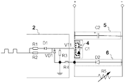
- the electronic contactor system provided in this embodiment includes an electronic contactor, a load, and a protection circuit.
- the electronic contactor includes a switch tube 1 and a driving circuit 2
- the protection circuit includes a first voltage absorbing circuit. 4.
- the power input end of the switch tube 1 is connected to the positive end of the power source, the power output end is connected to the negative end of the power supply through the load 3, and the drive signal access end is connected to the output end of the drive circuit 2; the input end of the drive circuit 2 and the drive signal source connection.
- the first voltage absorbing circuit 4 of the protection circuit is connected to the power input terminal and the power output terminal of the switching transistor 1, respectively.
- the driving signal can be generated in various manners, for example, by a digital processing chip DSP or a single chip microcomputer or an ARM processor, or can be driven by a timer chip. signal.
- the driving circuit 2 in this embodiment can also transmit the driving signal to the switching tube 1 by using any existing driving circuit.
- the driving signal in this embodiment may specifically be a square wave signal, and the signal frequency may be specifically selected according to current specific requirements, such as current demand, frequency requirements for controlling opening and closing, and the like.
- the switch tube 1 in this embodiment is specifically implemented by using various switch components, such as but not limited to a MOS transistor or a triode or an insulated gate bipolar transistor.
- the switch tube 1 is specifically a MOS tube
- the power input end of the switch tube 1 is a drain end, which is connected to the positive terminal of the power source, and the power output end is a source terminal, and is connected to the negative terminal of the power source.
- the power supply can be provided by various power supply systems.
- the first voltage absorbing circuit 6 is connected to the positive terminal of the power source, and is connected to the negative terminal of the power source through the load 3 to form a charging circuit, and the absorbing switch tube 1 is The voltage between the power input terminal and the power output terminal is charged, and the voltage spike between the power input end of the switch tube 1 and the power output end can be absorbed to prevent the voltage spike from damaging the switch tube, thereby reducing the use.
- the cost can improve the safety and stability of the circuit control.
- the first voltage absorbing circuit 6 is respectively connected to the power input end and the power output end of the switch tube to form a discharge circuit, and discharges the previously absorbed electric energy. It is expected that the next switch will be turned off to ensure the reliability and safety of the control.
- the first voltage absorbing circuit 6 in this embodiment may be composed of a first capacitor. At this time, the two ends of the first capacitor are respectively connected with the power input end of the switch tube and the power output end, and the internal resistance of the switch tube can be directly formed at this time.
- RC absorption circuit may also Add an external resistor directly to form an RC snubber circuit.
- the protection circuit in this embodiment further includes a second voltage absorbing circuit, as shown in FIG.
- the second voltage absorbing circuit 5 is respectively connected to the positive terminal of the power source (near the power input terminal of the switching transistor 1, for example, the drain terminal) and the negative terminal of the power supply.
- the driving circuit 2 inputs the driving signal to control the switching tube 1 to be turned off
- the equivalent inductance of the wire of the positive input terminal of the system power source generates an induced voltage
- the second voltage absorbing circuit 5 is respectively connected with the positive terminal of the power source and the negative terminal of the power source to form a charging circuit.
- the induced voltage generated by the positive terminal of the power source is absorbed to charge, so as to eliminate the influence of the inductance of the wire, thereby further reducing the voltage applied to the drain and the source of the switch, thereby ensuring the safety and reliability of the switch.
- the driving circuit 2 inputs the driving signal to control the switching tube 1 to communicate
- the second voltage absorbing circuit 5 and the switching tube 1 power input end and the load output end are connected to each other, and the switching tube 1 and the load 3 form a discharge circuit for discharging, so that the lower Prepare the shutdown of the switch 1 once.
- the second voltage absorbing circuit 5 in this embodiment includes a second capacitor connected to the positive terminal of the power source and the negative terminal of the power supply at both ends.
- the capacitance value of the second capacitor in this embodiment is greater than or equal to 16384 microfarads.
- the corresponding capacitance value can be flexibly selected according to a specific application scenario.
- first voltage absorbing circuit and the second voltage absorbing circuit in this embodiment can theoretically adopt any circuit capable of realizing voltage absorption and charging and discharging. It is not limited to the manner in which the above-described capacitor is used to form the charge and discharge circuit.
- the output cable is also long, and its equivalent inductance is large.
- the switch tube 1 When the switch tube 1 is turned off, the energy accumulated in the part of the cable also needs to be released. Therefore, the power output of the switch tube 1 is also in this embodiment.
- the end side is provided with an energy absorbing circuit, as shown in FIG. 4, the energy absorbing circuit 6 is connected Between the output end of the switch tube 1 and the negative end of the power supply, an energy absorption circuit is formed with the load 3; when the switch tube 1 is turned off, the energy stored in the inductance of the wire in the energy absorption circuit 5 is released through the load 3 to eliminate the switch tube.
- the influence of the inductance of the output side wire further enhances the safety and reliability of the electronic contactor.
- the energy absorbing circuit 6 in this embodiment includes a unidirectional conduction device connected between the output end of the switching tube and the negative terminal of the power supply, and the positive terminal of the unidirectional conduction device is connected to the negative terminal of the power supply.
- the single-conductor in this embodiment can theoretically employ any component capable of implementing a unidirectional conduction function, such as a diode.
- a corresponding protection circuit can be respectively disposed on the power input end side of the switch tube, the power input end and the power output end, and the power output end side to prevent the switch tube from being damaged during the large current switching process, and the control is ensured. Safety and reliability.
- the switching transistor is a MOS transistor
- the driving signal is a square wave signal
- the first voltage absorbing circuit and the second voltage absorbing circuit are composed of a capacitor (for example, an electrolytic capacitor)
- the energy absorbing circuit is composed of a diode D2.
- Composition for example, silicon carbide diode.
- FIG. 6 shows that when the MOS transistor VT1 is switched from the communication to the shutdown under the control of the driving signal input by the driving circuit 2, the positive input terminal of the C1 is connected to the positive terminal of the power supply, and the negative output terminal is passed.
- the load R5 is connected to the negative terminal of the power supply, and the absorption circuit of the voltage spike between the drain (ie, the power input terminal) and the source (ie, the power output terminal) of the MOS transistor VT1 is shown by the arrow of the dotted line in FIG.
- the figure shows that the MOS transistor VT1 is switched from off to connected under the control of the driving signal input from the driving circuit 2.
- the positive input terminal of the C1 is connected to the drain of the MOS transistor VT1, and the negative electrode is connected.
- the output end is in communication with the source of the MOS transistor VT1, and forms a discharge loop with the internal resistance of the MOS transistor VT1.
- the circuit of the C1 discharge is shown by the arrow of the dotted line in FIG.
- the MOS transistor is discharged to the capacitor C1 before the next turn-off, in preparation for charging for the next absorption voltage.
- FIG. 8 shows that the MOS transistor VT1 is switched from the communication to the shutdown under the control of the driving signal input by the driving circuit 2, and the C2 positive input terminal is connected to the positive terminal of the power supply, and the negative output terminal is directly connected. Connected to the negative terminal of the power supply to form a charging circuit.
- the inductor voltage generated by the wire at the positive terminal of the power supply charges C2 through C2 absorption.
- the specific charging circuit is shown by the arrow of the dotted line in Figure 8, and the source positive terminal can be eliminated.
- the inductance of the part of the wire affects the voltage, further reducing the voltage applied to the drain and source of the MOS transistor.
- the driving circuit 2 inputs the driving signal to control the MOS transistor VT1 to communicate, the drains of C2 and VT1 and the output of the load R5 are turned on, and the discharge circuit is formed with the MOS tube VT1 and the load R5, and the previously stored power is turned off once in the MOS tube. Release before the break, in order to prepare for the next absorption voltage.
- FIG. 9 shows the MOS tube source VT1 under the control of the driving signal input by the driving circuit 2, when switching from the communication to the off, the energy absorption circuit composed of the diode D2 and the load 3 can be used as the MOS tube source.
- the energy stored in the inductor below the terminal and in the energy absorbing loop is released through the load R5 to eliminate the influence of the inductance of the MOS drain output side conductor, thereby further improving the safety and reliability of the electronic contactor.
- the switch tube in the present invention is not limited to the MOS tube, and other tube devices capable of implementing the break control may be employed; the voltage sink circuit is not limited to the above manner implemented by the capacitor; and the energy absorption circuit is not It is limited to the specific one-way device through the diode, and other components can be replaced according to actual needs.
- the above is only a specific embodiment of the present invention, and is not intended to limit the present invention in any way. Any simple modification, equivalent change, combination or modification of the above embodiments in accordance with the technical spirit of the present invention is still in the present invention. The scope of protection of the technical solution of the invention.
Landscapes
- Emergency Protection Circuit Devices (AREA)
Abstract
La présente invention concerne un circuit de protection et un système de contacteur électronique. Une extrémité d'entrée de puissance d'un tube de commutation (1) d'un contacteur électronique est connectée à une extrémité positive d'une source de puissance, et une extrémité de sortie de puissance est connectée à une extrémité négative de la source de puissance au moyen d'une charge (3); une borne d'accès de signal de commande est connectée à une extrémité de sortie d'un circuit de commande (2), et un premier circuit d'absorption de tension (4) d'un circuit de protection est connecté à l'extrémité d'entrée de puissance et l'extrémité de sortie de puissance du tube de commutation (1), respectivement; lorsque le tube de commutation (1) est commandé par un signal de commande pour être désactivé, le premier circuit d'absorption de tension (4) est connecté à l'extrémité positive de la source de puissance, et est connecté à l'extrémité négative de la source de puissance au moyen de la charge (3) pour former un circuit de charge. À ce stade, une tension entre l'extrémité d'entrée de puissance et l'extrémité de sortie de puissance du tube de commutation (1) est absorbée et chargée, c'est-à-dire que la tension de crête entre l'extrémité d'entrée de puissance et l'extrémité de sortie de puissance du tube de commutation (1) est absorbée de façon à empêcher la tension de crête d'endommager le tube de commutation (1), de façon à réduire les coûts d'utilisation et améliorer la sécurité et la stabilité de commandes de circuit.
Applications Claiming Priority (2)
| Application Number | Priority Date | Filing Date | Title |
|---|---|---|---|
| CN201610280486.8A CN107332543A (zh) | 2016-04-28 | 2016-04-28 | 一种电子接触器的保护电路及系统 |
| CN201610280486.8 | 2016-04-28 |
Publications (1)
| Publication Number | Publication Date |
|---|---|
| WO2017186028A1 true WO2017186028A1 (fr) | 2017-11-02 |
Family
ID=60161862
Family Applications (1)
| Application Number | Title | Priority Date | Filing Date |
|---|---|---|---|
| PCT/CN2017/080923 WO2017186028A1 (fr) | 2016-04-28 | 2017-04-18 | Circuit de protection et système de contacteur électronique |
Country Status (2)
| Country | Link |
|---|---|
| CN (1) | CN107332543A (fr) |
| WO (1) | WO2017186028A1 (fr) |
Families Citing this family (2)
| Publication number | Priority date | Publication date | Assignee | Title |
|---|---|---|---|---|
| CN109450652A (zh) * | 2018-11-26 | 2019-03-08 | 珠海世讯科技有限公司 | 一种knx总线供电电路 |
| CN117562649A (zh) * | 2023-11-21 | 2024-02-20 | 邦士医疗科技股份有限公司 | 一种陡脉冲消融急停释能控制系统 |
Citations (5)
| Publication number | Priority date | Publication date | Assignee | Title |
|---|---|---|---|---|
| CN2269672Y (zh) * | 1996-06-25 | 1997-12-03 | 中国航天工业总公司第一研究院第十五研究所 | 高压高频大功率斩波器 |
| US6373731B1 (en) * | 2000-02-28 | 2002-04-16 | Hitachi, Ltd. | Surge voltage suppressed power inverter using a voltage driven switching element |
| CN102097796A (zh) * | 2010-12-30 | 2011-06-15 | 广东易事特电源股份有限公司 | 太阳能充电控制器的功率开关管的电压尖峰吸收保护电路 |
| CN104242265A (zh) * | 2014-08-29 | 2014-12-24 | 荣信电力电子股份有限公司 | 一种直流配电网全固态直流断路器 |
| CN204046154U (zh) * | 2014-04-21 | 2014-12-24 | 西安霍威电源有限公司 | 80v尖峰浪涌抑制模块 |
Family Cites Families (3)
| Publication number | Priority date | Publication date | Assignee | Title |
|---|---|---|---|---|
| US9143092B2 (en) * | 2011-12-14 | 2015-09-22 | Maxim Integrated Products, Inc. | Fully capacitive coupled input choppers |
| CN202840932U (zh) * | 2012-10-11 | 2013-03-27 | 淄博山大奥太电气有限公司 | 逆变焊机igbt尖峰电压保护装置 |
| CN104868458B (zh) * | 2015-05-27 | 2018-09-28 | 山东电工电气日立高压开关有限公司 | 一种感应电压吸收装置及其方法 |
-
2016
- 2016-04-28 CN CN201610280486.8A patent/CN107332543A/zh active Pending
-
2017
- 2017-04-18 WO PCT/CN2017/080923 patent/WO2017186028A1/fr active Application Filing
Patent Citations (5)
| Publication number | Priority date | Publication date | Assignee | Title |
|---|---|---|---|---|
| CN2269672Y (zh) * | 1996-06-25 | 1997-12-03 | 中国航天工业总公司第一研究院第十五研究所 | 高压高频大功率斩波器 |
| US6373731B1 (en) * | 2000-02-28 | 2002-04-16 | Hitachi, Ltd. | Surge voltage suppressed power inverter using a voltage driven switching element |
| CN102097796A (zh) * | 2010-12-30 | 2011-06-15 | 广东易事特电源股份有限公司 | 太阳能充电控制器的功率开关管的电压尖峰吸收保护电路 |
| CN204046154U (zh) * | 2014-04-21 | 2014-12-24 | 西安霍威电源有限公司 | 80v尖峰浪涌抑制模块 |
| CN104242265A (zh) * | 2014-08-29 | 2014-12-24 | 荣信电力电子股份有限公司 | 一种直流配电网全固态直流断路器 |
Also Published As
| Publication number | Publication date |
|---|---|
| CN107332543A (zh) | 2017-11-07 |
Similar Documents
| Publication | Publication Date | Title |
|---|---|---|
| RU2665683C1 (ru) | Топология схемы демпфирования токов короткого замыкания, метод и преобразователь на ее основе | |
| US9276401B2 (en) | Solid state circuit-breaker switch devices | |
| CN103346763B (zh) | 一种绝缘栅双极晶体管驱动保护电路 | |
| US10748724B2 (en) | Power-on/off drive circuit and method for controlling power-on/off drive circuit | |
| TWI661675B (zh) | 功率半導體開關的驅動電路 | |
| EP3883112B1 (fr) | Convertisseur acf, procédé de conversion de tension et dispositif électronique | |
| US20140177308A1 (en) | Electrical power conversion device | |
| US11862416B2 (en) | Hybrid DC circuit breaker | |
| CN110830015A (zh) | 功率半导体元件的驱动保护电路及其控制方法 | |
| CN108847835B (zh) | 一种功率器件驱动保护电路及其控制方法 | |
| US11239746B2 (en) | Two-stage converter and method for starting the same, LLC converter, and application system | |
| WO2017186028A1 (fr) | Circuit de protection et système de contacteur électronique | |
| US9819291B2 (en) | Direct-current motor control device | |
| CN105720802A (zh) | 一种h桥全功能igbt隔离驱动控制模块 | |
| CN109391135B (zh) | 一种掉电保持电路以及开关电源 | |
| US7969225B2 (en) | Circuit of reducing power loss of switching device | |
| CN105977939A (zh) | 一种直流源保护装置与方法 | |
| KR100916047B1 (ko) | 무손실 역률 개선 회로 | |
| CN109450418A (zh) | 一种带开关控制单元的igbt隔离驱动电路及其控制方法 | |
| CN203193500U (zh) | 一种开关电源及其充电回路 | |
| CN104952664A (zh) | 一种无电弧放电的直流高压开关 | |
| TWI777735B (zh) | 具有被動式無損失緩衝器之升壓轉換裝置 | |
| CN105099196A (zh) | 一种电源变换器 | |
| JP6459130B2 (ja) | 電力変換装置及びそれを用いたパワーコンディショナ | |
| CN203617897U (zh) | 一种功率开关管的保护及缓冲电路 |
Legal Events
| Date | Code | Title | Description |
|---|---|---|---|
| NENP | Non-entry into the national phase |
Ref country code: DE |
|
| 121 | Ep: the epo has been informed by wipo that ep was designated in this application |
Ref document number: 17788680 Country of ref document: EP Kind code of ref document: A1 |
|
| 122 | Ep: pct application non-entry in european phase |
Ref document number: 17788680 Country of ref document: EP Kind code of ref document: A1 |