WO2017170744A1 - 光学素子、周期構造体、光学素子の製造方法及び周期構造体の製造方法 - Google Patents
光学素子、周期構造体、光学素子の製造方法及び周期構造体の製造方法 Download PDFInfo
- Publication number
- WO2017170744A1 WO2017170744A1 PCT/JP2017/013021 JP2017013021W WO2017170744A1 WO 2017170744 A1 WO2017170744 A1 WO 2017170744A1 JP 2017013021 W JP2017013021 W JP 2017013021W WO 2017170744 A1 WO2017170744 A1 WO 2017170744A1
- Authority
- WO
- WIPO (PCT)
- Prior art keywords
- curable resin
- surface layer
- optical element
- thickness
- wall surfaces
- Prior art date
- Legal status (The legal status is an assumption and is not a legal conclusion. Google has not performed a legal analysis and makes no representation as to the accuracy of the status listed.)
- Ceased
Links
Images





Classifications
-
- B—PERFORMING OPERATIONS; TRANSPORTING
- B29—WORKING OF PLASTICS; WORKING OF SUBSTANCES IN A PLASTIC STATE IN GENERAL
- B29C—SHAPING OR JOINING OF PLASTICS; SHAPING OF MATERIAL IN A PLASTIC STATE, NOT OTHERWISE PROVIDED FOR; AFTER-TREATMENT OF THE SHAPED PRODUCTS, e.g. REPAIRING
- B29C59/00—Surface shaping of articles, e.g. embossing; Apparatus therefor
- B29C59/02—Surface shaping of articles, e.g. embossing; Apparatus therefor by mechanical means, e.g. pressing
-
- G—PHYSICS
- G02—OPTICS
- G02B—OPTICAL ELEMENTS, SYSTEMS OR APPARATUS
- G02B5/00—Optical elements other than lenses
- G02B5/08—Mirrors
-
- G—PHYSICS
- G02—OPTICS
- G02B—OPTICAL ELEMENTS, SYSTEMS OR APPARATUS
- G02B5/00—Optical elements other than lenses
- G02B5/08—Mirrors
- G02B5/09—Multifaceted or polygonal mirrors, e.g. polygonal scanning mirrors; Fresnel mirrors
Definitions
- the present invention can be applied to an optical element having reflectors arranged in a matrix and a periodic structure having a similar structure.
- Patent Documents 1 and 2 and Non-Patent Document 1 disclose a configuration in which an image is displayed in the air using an optical element in which reflectors are arranged in a matrix.
- Patent Documents 1 and 2 disclose optical elements in which the reflector is formed by convex portions and concave portions each having a quadrangular prism shape.
- this reflector is formed by a pair of reflecting surfaces that intersect (orthogonally) so as to form an angle of 90 degrees.
- the reflector reflects incident light in the incident direction in the in-plane direction of the plane orthogonal to the pair of reflecting surfaces, whereas in the vertical direction of the plane, the reflector reflects the incident light at a reflection angle corresponding to the incident angle.
- the optical element a large number of reflectors are manufactured and arranged in a matrix.
- the optical element reflects and collects the emitted light emitted from various object points in various directions, and forms image points corresponding to the object points in the space.
- this optical element forms a large number of image points corresponding to a large number of object points on a space corresponding to each object point, and displays an image in the air.
- Such an image display in the air can be applied in various ways.
- An element having such a reflector can also be used when measuring changes over time such as the concentration of various solutions as disclosed in Patent Documents 3 to 5, for example. Therefore, in the future, devices having such a structure can be applied to various fields.
- JP 2008-158114 A Special table 2012-163702 gazette JP 2006-337351 A JP 2011-057819 A Japanese Patent Laying-Open No. 2005-077396
- the present invention has been made in view of such a situation, and an object of the present invention is to enable mass production with high accuracy and simple, with respect to an optical element in which reflectors are arranged in a matrix and a periodic structure having a similar structure.
- the present inventor has intensively studied to solve the above-mentioned problems, and prepared an uneven surface layer by forming treatment, and provided a foundation with a certain thickness on the uneven surface layer, and changed the shape at the time of curing. This led to the idea of reducing the amount of light and completed the present invention.
- the present invention provides the following.
- a base material An uneven surface layer formed by a cured product of a curable resin formed on the substrate, In the uneven surface layer, concave portions having first and second wall surfaces orthogonal to each other are arranged in a matrix, An optical element comprising a cured product of the curable resin having a thickness of 19 ⁇ m or more and 150 ⁇ m or less at the bottom of the recess.
- a concave / convex surface layer is formed using a curable resin by providing a cured product of a curable resin with a thickness of 19 ⁇ m or more and 150 ⁇ m or less at the bottom of the concave portion, the concave portion due to curing shrinkage.
- the deterioration of the wall shape can be sufficiently reduced by the curable resin at the bottom.
- it can be easily produced by applying the shaping process, and mass production can be performed with high accuracy.
- the recess is Comprising third and fourth wall surfaces facing the first and second wall surfaces, respectively;
- the mold for molding formed by arranging the convex portions by the quadrangular prism shape in a matrix is used.
- the mold for molding having such a shape can be easily and highly accurately manufactured by repeatedly forming concave grooves intersecting at right angles by cutting, thereby further easily and highly accurately optical elements.
- the concave portion has a tapered shape, it is possible to reduce the burden on the cutting tool when the molding die is manufactured. Moreover, mold release can also be improved and accuracy can be further improved.
- the first and second wall surfaces are An optical element having an arithmetic average roughness Ra of 2 nm to 260 nm.
- the depth of the recess is An optical element that is larger than the thickness of the cured product of the curable resin provided on the bottom.
- the bottom is An optical element that is parallel to the surface of the substrate and has a flat planar shape.
- the light from one object point can be accurately focused on one image point without causing an unnecessary diffusing action on the light transmitted through the bottom, and is provided for display.
- the image quality can be improved.
- the recess is The repetition pitch P is 40 ⁇ m or more and 400 ⁇ m or less,
- the width W1 is 20 ⁇ m or more and 200 ⁇ m or less,
- a base material An uneven surface layer formed by a cured product of a curable resin formed on the substrate, In the uneven surface layer, convex portions having first and second orthogonal wall surfaces are arranged in a matrix, An optical element provided with a cured product of the curable resin with a thickness of 19 ⁇ m or more and 150 ⁇ m or less between adjacent convex portions.
- the gap between adjacent convex portions is determined.
- the deterioration of the convex wall surface due to curing shrinkage can be sufficiently reduced by the curable resin.
- it can be easily produced by applying the shaping process, and mass production can be performed with high accuracy.
- (9) a base material; An uneven surface layer formed by a cured product of a curable resin formed on the substrate, In the uneven surface layer, recesses having adjacent first and second wall surfaces are arranged in a matrix, A periodic structure having a cured product of the curable resin with a thickness of 19 ⁇ m or more and 150 ⁇ m or less at the bottom of the recess.
- the concave / convex surface layer is formed by a forming process using a curable resin and the concave portions are arranged in a matrix to form the concave / convex surface layer, the concave shape due to curing shrinkage is formed. Can be sufficiently reduced. As a result, the periodic structure can be easily produced, and the periodic structure can be mass-produced with high accuracy.
- (10) a base material; An uneven surface layer formed by a cured product of a curable resin formed on the substrate, In the uneven surface layer, convex portions having adjacent first and second wall surfaces are arranged in a matrix, A periodic structure provided with a cured product of the curable resin with a thickness of 19 ⁇ m or more and 150 ⁇ m or less between the adjacent convex portions.
- the concavo-convex surface layer is produced using a curable resin and the concavo-convex surface layer is formed by arranging the concavo-convex surface layer in a matrix, the convex wall surface shape due to curing shrinkage is formed. Can be sufficiently reduced. As a result, the periodic structure can be easily produced, and the periodic structure can be mass-produced with high accuracy.
- (11) it can be easily mass-produced by being able to be produced using a curable resin.
- a curable resin to the bottom of the recess so as to produce a cured product of the curable resin with a thickness of 19 ⁇ m or more and 150 ⁇ m or less, it is possible to sufficiently reduce the deterioration of the recess wall shape due to curing shrinkage. Can be mass-produced with high accuracy.
- (12) since it can be produced using a curable resin, it can be easily mass-produced.
- the curable resin by coating the curable resin with a thickness that produces a cured product of a curable resin with a thickness of 19 ⁇ m or more and 150 ⁇ m or less between the convex portions, the deterioration of the convex wall surface shape due to curing shrinkage can be sufficiently reduced. Can be mass-produced with high accuracy.
- a method for producing a periodic structure in which a concave and convex surface layer formed by arranging concave portions having adjacent first and second wall surfaces in a matrix is formed on a base material A coating step of coating the base material with a coating solution of a curable resin; The substrate for which the coating liquid of the curable resin is applied is pressed against a molding die having a surface shape corresponding to the surface shape of the uneven surface layer to cure the curable resin, A curing step for producing an uneven surface layer having a surface shape corresponding to the surface shape of the mold for the mold, A peeling step of peeling the uneven surface layer integrally with the base material,
- the manufacturing method of the periodic structure which coats the coating liquid of the said curable resin by the thickness which produces the hardened
- (14) it can be easily mass-produced by using a curable resin. Also, by applying a curable resin with a thickness that produces a cured product of a curable resin with a thickness of 19 ⁇ m or more and 150 ⁇ m or less between the convex portions, the deterioration of the concave wall surface shape due to curing shrinkage can be sufficiently reduced. Can be mass-produced with high accuracy.
- an optical element in which reflectors are arranged in a matrix and a periodic structure having a similar structure can be easily mass-produced with high accuracy.
- FIG. 7 is a diagram for explaining a byte used in the process of FIG. 6. It is a flowchart which shows the manufacturing process of the optical element of FIG. It is a characteristic curve figure which shows the evaluation result of the wall surface of an optical element. It is a figure which shows the optical element which concerns on 2nd Embodiment.
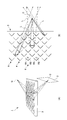
- FIG. 1A is a schematic diagram illustrating the image display apparatus according to the first embodiment.
- the image display device 1 displays a desired image in a space.
- the image display device 1 is provided with an image display panel 2 such as a liquid crystal display panel, and an image for display in space is displayed on the panel surface of the image display panel 2.
- an optical element 3 is disposed between the image display panel 2 and an area used for spatial display of an image.
- the image display device 1 forms an image point Q corresponding to the object point O on the panel surface of the image display panel 2 in the space by the optical element 3, thereby displaying a desired image in the space. As shown in FIG.
- the image producing means for producing an image for display is not limited to the case of producing a two-dimensional image by applying the image display panel 2, and various configurations can be widely applied. You may apply the image formation means of a three-dimensional image.
- the arrangement of the optical element 3 is not limited to the configuration shown in FIG. 1, and various configurations can be widely applied, and also widely applied when used in combination with a sensing means such as an imaging means. can do.
- the optical element 3 has a reflector 6 formed by a pair of orthogonal reflecting surfaces RA and RB as schematically shown in FIG. 1B when the surface is viewed from the vertical direction, and the reflector 6 is small. A large number are arranged in a matrix. More specifically, the pair of reflection surfaces RA and RB are arranged so as to intersect at an intersection angle ⁇ of 90 degrees.
- the reflector 6 is set so that a straight line intersecting the reflection surfaces RA and RB is substantially parallel to a straight line connecting the object point O and the image point Q, and further, the reflected light from the image display panel 2 is reflected on the reflection surface RA. Or it arrange
- the image display apparatus in the in-plane direction shown in FIG. 1, the emitted light L emitted from a number of object points O in various directions by the number of reflectors 6 is reflected and condensed in the incident direction, An image point Q corresponding to each object point O is formed in the space, and an image is displayed in the air.
- the reflected light is directed toward the image point Q with a certain extent.
- the optical element 3 is provided with an uneven surface layer 8 having a fine uneven surface on a base material 7.
- the concavo-convex surface layer 8 is formed of a cured product of a curable resin by being manufactured by a molding process using a curable resin. More specifically, it is formed of a cured product of an ultraviolet curable resin.
- the concave / convex surface layer 8 is formed by arranging the concave portions 9 having the first and second wall surfaces K1 and K2 corresponding to the reflective surfaces RA and RB in a matrix by using a molding die for the molding process. It is formed by the surface shape which becomes.
- a periodic structure 10 having a periodic structure of a basic shape corresponding to the reflector 6 is formed by the base material 7 and the uneven surface layer 8.
- the optical element 3 is formed by arranging the periodic structure 10 on a transparent support as necessary.
- the reflecting surfaces RA and RB are formed by the concave portions 9 related to the periodic structure 10, and the reflector 6 is manufactured.
- the recess 9 is formed in a quadrangular prism shape.
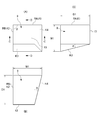
- FIG. 3A is a plan view of the recess 9 as viewed from the opening side (upper side in FIG. 2), and FIGS. 3B and 3C are a CC line and a DD line, respectively. It is sectional drawing of the recessed part 9 cut out and shown by.
- the periodic structure 10 has an angle formed by the adjacent first and second wall surfaces K1 and K2 when the concave portion 9 is formed in a quadrangular prism shape and the cross-section is taken by a plane parallel to the surface of the base material 7.
- ⁇ is formed by the intersection angle ⁇ of the reflection surfaces RA and RB.
- the reflection surfaces RA and RB are formed by the wall surfaces K1 and K2.
- the optical element 3 reflects the incident light with a large number of reflectors 6 to produce the image point Q, and this intersection angle ⁇ determines the accuracy of the optical path to the image point Q corresponding to the object point O.
- the angle of 90 degrees is ensured with high accuracy, the light emitted from the object point O can be condensed at one point, and as a result, the resolution and luminance can be improved. Accordingly, it is desirable to set the crossing angle ⁇ to 90 degrees as much as possible.
- the two adjacent wall surfaces having an intersecting angle ⁇ within 90 ° ⁇ 1 Is preferably within 90 ° ⁇ 1 °, and more preferably the crossing angle ⁇ is within 90 ° ⁇ 0.5 °.
- the orthogonal angle between the reflecting surfaces RA and RB is preferably within 90 ° ⁇ 1, but more preferably within 90 ° ⁇ 0.5 °.
- the reflective surfaces RA and RB are formed by disposing metal thin films on the adjacent first and second wall surfaces K1 and K2 forming the crossing angle ⁇ in the periodic structure 10 by vapor deposition or the like.
- the first and second wall surfaces K1 and K2 may be used as the reflection surfaces RA and RB without providing the metal thin film as necessary.
- the optical element 3 it is only necessary to arrange a large number of reflectors 6 to produce an image point Q corresponding to the object point O.
- the reflector 6 has only a pair of orthogonal reflecting surfaces RA and RB. That's fine.
- the cross-sectional shape cut out by the plane parallel to the base material 7 is an arc shape.
- a certain curved surface may be used, and the cross-sectional shape may be a flat surface that is a straight line connecting the tips of the reflecting surfaces RA and RB.
- the concave portion 9 can be applied with a quadrangular prism shape, a quadrangular pyramid shape, a quadrangular pyramid shape, and the like. Furthermore, a polygonal columnar shape, a cone shape, and a frustum shape in which a wall surface excluding the reflecting surfaces RA and RB is a polyhedral wall surface having three or more surfaces can be applied.
- the concave portion 9 is formed in a quadrangular prism shape, so that a pair of wall surfaces K3 and K4 similar to the pair of wall surfaces K1 and K2 related to the reflection surfaces RA and RB are formed on the reflection surface RA, It is formed in the concave portion 9 on the side facing the RB.
- the shaping die used for preparation of the optical element 3 can be produced simply so that it may mention later.
- the concave portion 9 having a quadrangular prism shape is formed in this way, and the concave portions 9 are repeatedly arranged at a constant pitch in the extending direction of the wall surfaces K1, K2, K3, and K4. In this manufacturing process, the mold can be easily and accurately manufactured.
- the first and second wall surfaces K1, K2 are produced with an arithmetic average roughness Ra of 2 nm to 260 nm, preferably 20 nm to 200 nm, more preferably 50 nm to 150 nm.
- arithmetic mean roughness Ra is based on JISB0601 (1994) here.
- the first and second wall surfaces K1, K2 may be configured to satisfy only the upper limit value of the arithmetic average roughness Ra. Further, when the arithmetic average roughness Ra of the first and second wall surfaces K1 and K2 is larger than 260 nm, the light reflected by the reflection surfaces RA and RB (first and second wall surfaces K1 and K2) is diffused, It is not preferable because light from one object point cannot be accurately focused on one image point, and image quality deteriorates such as image blurring or image whitening.
- the arithmetic average roughness Ra of the first and second wall surfaces K1 and K2 satisfy the above range. It should be noted that some stray light or the like is incident on the third and fourth wall surfaces K3 and K4 facing the first and second wall surfaces K1 and K2, and is diffused unnecessarily, and the transparency of the optical element 3 is reduced. In addition, since the image quality may be deteriorated, the arithmetic average roughness Ra preferably satisfies the above range.
- the concave portion 9 is formed in a quadrangular prism shape in this way, and the pair of wall surfaces K3 and K4 facing the pair of wall surfaces K1 and K2 related to the reflection surfaces RA and RB are formed of a base material. 7 is formed in a tapered quadrangular prism shape that is inclined by an angle ⁇ toward the center direction of the recess 9 in the depth direction from the vertical plane L1 with respect to the surface 7.
- the optical element 3 is configured so as to be easily and accurately manufactured by using a mold for molding described later. Moreover, it is comprised so that the peelability from this mold for shaping
- the angle ⁇ is set to 1 degree or more and 45 degrees or less, but is preferably set to 5 degrees or more and 30 degrees or less, more preferably 10 degrees or more and 20 degrees or less. desirable.
- FIGS. 2B and 2C are cross-sectional views of FIG. 2A cut along lines AA and BB, respectively. It is sectional drawing cut out and shown by the cut surface extended in each direction.
- the recess 9 is formed with a square outer shape on the opening side.
- the concave portion 9 is formed with a width W1 (a size of one side of the square shape related to the opening-side cross-sectional shape of the concave portion 9) of 20 ⁇ m to 200 ⁇ m, preferably 20 ⁇ m to 100 ⁇ m, more preferably 20 ⁇ m to 50 ⁇ m. It is formed.
- the recesses 9 are formed such that the width W2 of the wall 12 between the recesses 9 is 20 ⁇ m or more and 200 ⁇ m or less, preferably 20 ⁇ m or more and 100 ⁇ m or less, and more preferably 20 ⁇ m or more and 50 ⁇ m or less.
- the recess 9 is formed with a depth D1 of 20 ⁇ m or more and 600 ⁇ m or less, preferably 100 ⁇ m or more and 500 ⁇ m or less, more preferably 200 ⁇ m or more and 300 ⁇ m or less.
- the pitch P is 40 ⁇ m or more and 400 ⁇ m or less, preferably 60 ⁇ m or more and 300 ⁇ m or less, more preferably 100 ⁇ m or more and 200 ⁇ m or less.
- the wall 12 between the recesses 9 is formed on the surface of the base material 7 by the height according to the depth D1 larger than the width W2. Will be produced.
- the wall surfaces K1 to K4 related to the recess 9 it was found that the production accuracy was significantly deteriorated. This deterioration in accuracy becomes more prominent as the aspect ratio is higher. Therefore, when the aspect ratio is 0.05 or more, 30 or less, preferably 2 or more and 20 or less, more preferably 5 or more and 10 or less, in this embodiment, an optical device whose accuracy is significantly deteriorated due to an increase in the aspect ratio. With respect to the element, manufacturing accuracy can be improved.
- This deterioration in accuracy is considered to be due to hardening shrinkage of the shaping resin, and is manifested by a decrease in the smoothness (meandering) of the wall surfaces K1 to K4, and a roughening of the wall surfaces K1 to K4. It is considered that the crossing angle ⁇ also deteriorates due to the meandering of the wall surfaces K1 to K4.
- the smoothness of the wall surfaces K1 to K4 decreases because the light from one object point O reflected by many reflectors 6 cannot be focused on one point, thereby reducing the resolution and brightness level of the image displayed in space.
- the image quality is degraded.
- the wall surfaces K1 to K4 are roughened, the light reflected by the reflector 6 cannot be collected at one point, so that the resolution and luminance level of the image displayed in the space are lowered and the image quality is deteriorated. I will let you.
- the cured product of the curable resin used for the shaping process of the recess 9 remains on the bottom 13 of the recess 9 with a thickness D2 of 19 ⁇ m or more and 150 ⁇ m or less.
- the wall surfaces K1 and K2 manufactured on the wall portion 12 having a high aspect ratio as described above, and the wall surfaces K1 and K2 that require surface accuracy are held so as to face the corresponding wall surfaces K3 and K4. If the cured product of the shaping resin remains in the bottom portion 13 of the recess 9 between the wall surfaces K1 and K3 and between the wall surfaces K2 and K4, the curable resin is cured in the shaping process.
- the shaping resin on the bottom portion 13 alleviates deformation and roughening of the wall surfaces K1 to K4 due to curing shrinkage of the curable resin of the wall portion 12 related to the wall surfaces K1 to K4.
- the accuracy of the reflective surfaces RA and RB can be improved, and the optical element 3 can be mass-produced with high accuracy.
- the upper limit value of the thickness of the cured product at the bottom 13 is a limitation due to significant deterioration of productivity due to intense curling as the thickness increases, as will be described later. Thereby, when it is not necessary to consider the deterioration of productivity due to curling, it can be configured to satisfy only the lower limit value. Moreover, it is preferable that the depth D1 of the recessed part 9 is larger than the thickness D2 of the hardened
- the optical element 3 can be mass-produced with high accuracy by the mold processing.
- the thickness D2 of the cured product at the bottom 13 of the recess 9 is preferably 19 ⁇ m or more and 150 ⁇ m or less, more preferably 19 ⁇ m or more and 60 ⁇ m or less.
- the thickness D2 is less than 19 ⁇ m, the appearance defect of the optical element 3 increases as will be described later, which is not suitable for use.
- the thickness D2 is larger than 150 ⁇ m, as will be described later, curling or the like is likely to occur during the manufacturing process, and the degree of curling becomes stronger as the thickness increases, which is not suitable for mass production. Therefore, it is desirable that the thickness D2 satisfy the above range.
- the bottom portion 13 of the concave portion 9 is formed by a plane parallel to the surface of the base material 7, and the thickness D2 of the cured product at the bottom portion 13 of the concave portion 9 is the above-described thickness at each portion in the in-plane direction.
- the shape of the bottom portion 13 for example, by applying various shapes for the purpose of improving the releasability during the shaping process, for example, in the cross-sectional shape in FIGS. It may be set to a shape, a slanted slope shape, a downwardly convex triangular shape, a sawtooth shape, etc.
- the thickness of the part where the distance between the surface of the base material 7 in each cross section is the smallest D2 is set to the above-mentioned thickness.
- the bottom 13 of the recess 9 is parallel to the surface of the base material 7 and is flat (roughness) as shown in this embodiment, when importance is placed on improving the image quality of the image displayed by the optical element 3. Is small). Thereby, the light from one object point is not exerted on the light that passes through the bottom portion 13 and is reflected by the reflection surfaces RA and RB (first and second wall surfaces K1 and K2). Can be accurately focused on one image point, and deterioration in image quality such as blurring of an image displayed by the optical element 3 can be suppressed.
- the concave / convex surface layer 8 in which the quadrangular prism-shaped concave portions 9 are arranged in a matrix is formed by a shaping process using a curable resin, compared to a case where the bottom portion 13 is not flat and flat.
- various curable resins necessary for the shaping process can be applied to the uneven surface layer 8, for example, acrylic resin, polyester, epoxy resin, polyolefin, styrene resin, polyamide, polyimide, polyamide Imide, polyurethane, polyvinyl acetate, polyvinyl alcohol, polyvinyl butyral, polycarbonate, melamine resin, urea resin, alkyd resin, phenol resin, cellulose resin, diallyl phthalate resin, silicone resin, polyarylate resin, polyacetal resin, styrene-isoprene rubber, etc.
- the photo-curable resin can be applied.
- an ultraviolet curable resin as the resin forming the uneven surface layer 8.
- an acrylic resin can be applied.
- the base material 7 can be applied to this type of shaping process, and various film materials, plate materials, and the like that are transparent in a wavelength band used for image display can be applied. Thereby, the base material 7 can apply various transparent film materials, transparent sheet materials, and transparent plate materials used for the shaping process of this type of optical element.
- polycarbonate, PET (polyester), or the like can be applied to the transparent film material or the transparent sheet material, and a glass plate material, a polycarbonate plate material, or the like can be applied to the transparent plate material.
- FIG. 4 (A) is a diagram showing a molding die 20 used for manufacturing the periodic structure 10 of the optical element 3, and FIG. 4 (B) is a convex provided on the molding die 20. It is a perspective view which shows the part 21 in detail.
- the molding die 20 is formed in a flat plate shape, and a convex portion 21 corresponding to the concave portion 9 is formed in a prismatic shape which is an inverted shape of the concave portion 9 on the molding processing surface 20A used for the molding processing. .
- the convex part 21 is formed in a matrix shape with the pitch P and the base side width W1 in the extending direction of each side of the rectangle.
- the convex portions 21 are formed by the wall surfaces L1 to L4 corresponding to the respective wall surfaces K1 to K4 of the concave portion 9, whereby the wall surface L1 and L2 corresponding to the wall surfaces K1 and K2 has an intersection angle ⁇ set to 90 degrees.
- the wall surfaces L3 and L4 corresponding to the wall surfaces K3 and K4 are produced with high smoothness so as to be parallel to the vertical surface with respect to the surface of the molding die 20, and the vertical surfaces with respect to the surface of the molding die 20 are Is formed so as to be inclined by an angle ⁇ .
- the top portion 23 of the convex portion 21 is formed by a flat surface corresponding to the bottom portion 13 of the concave portion 9.
- the molding die 20 is manufactured by cutting the surface of a base material made of a metal material.
- the mold for molding is suitable for this type of cutting and is formed of a metal material suitable for the mold for molding. More specifically, a processed layer made of copper, aluminum, or the like is provided on the surface of a base material made of stainless steel, steel, or the like, and a convex portion 21 is provided on this processed layer.
- the entire molding die 20 may be made of copper, aluminum or the like.
- FIG. 5 is a flowchart showing a manufacturing process of the molding die 20.
- FIG. 6 is a diagram for explaining each process in comparison with FIG.
- an electrolytic composite polishing method using a combination of an electrolytic elution action and a rubbing action by abrasive grains. To make it super mirror surface.
- the base material 22 is smoothed (FIG. 6A).
- a one-dimensional cutting process using a cutting tool is repeated, so that a groove corresponding to the width W2 between the recesses 9 is obtained by a pitch corresponding to the manufacturing pitch P of the recesses 9.
- a repetition of the fine groove 25 having a width is produced (FIG. 6B).
- the cutting tool has a tip formed in a comb shape so that a plurality of fine grooves 25 can be formed simultaneously in parallel. This shortens the time required for the cutting process in this process.
- a linear cutting process using a cutting tool is repeated to form a surface shape in which the convex portions 21 are arranged in a matrix to produce a mold for molding.
- the cutting tool 24 is formed with a cross-sectional shape corresponding to the cross-sectional shape of the recess 9 as shown in FIG.
- the cutting tool 24 can make a fine groove by cutting, and the cutting edge related to the cutting process can be widened at the base, thereby improving the strength of the cutting edge and reducing damage or the like. it can. Since the strength of the cutting tool can be improved in this manner, in this manufacturing process, the production efficiency of the molding die 20 can be improved and the productivity can be improved.
- the mass productivity of the optical element 3 is improved. can do. Further, since the cutting tool can be made strong, the moving speed of the cutting tool can be increased, and the productivity can be improved.
- the width W1 of the recess 9 is limited to about 20 ⁇ m, and when the width W1 is made smaller than this, the manufacturing accuracy of the wall surfaces L1 to L4 and the like tends to deteriorate. .
- the shape and the like of the wall surfaces L1 to L4 are sufficiently reproducible and accurate. It is difficult to ensure, so that the mold can be manufactured with high accuracy in this embodiment as compared with these other fine processing techniques.
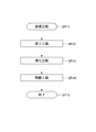
- FIG. 8 is a flowchart showing the manufacturing process of the optical element 3.
- the periodic structure 10 is manufactured and the optical element 3 is manufactured by executing the processing procedure shown in FIG. 8 by using the molding die 20 manufactured by the process shown in FIG. Make it.
- the curable resin coating solution is applied to the surface of the base material 7 by applying the coating liquid of the curable resin to the base material 7 and drying it.
- a curable resin coating liquid is applied to the bottom portion 13 of the concave portion 9 with a thickness for producing a cured product of the curable resin with a thickness of 19 ⁇ m or more and 150 ⁇ m or less by controlling the coating film thickness. .
- the optical element 3 is produced with high accuracy.
- the substrate 7 formed by forming the curable resin layer is pressed against the shaping mold 20 and pressed to be formed on the surface of the shaping mold 20.
- the curable resin material is sufficiently pressed against the fine uneven shape, and the curable resin is cured by irradiation with ultraviolet rays in this state. Thereby, in this process, the uneven surface layer 8 is produced with a curable resin.
- the uneven surface layer 8 is peeled off integrally from the base material 7 from the shaping mold 20, thereby producing the periodic structure 10.
- the optical element can be produced by a shaping process using a shaping mold, so that mass production can be easily performed.
- high accuracy can be secured by providing a cured product of a curable resin with a constant thickness on the bottom 13 of the recess 9.
- the separation starts from the side of the vertical wall surfaces K1 and K2 related to the recess 9, and the separation of the opposing wall surfaces K3 and K4 is after the vertical wall surfaces K1 and K2. And peel.
- peeling occurs in the direction indicated by the arrow F
- FIGS. 2B and 2C the peeling occurs in the direction indicated by the arrows F1 and F2.
- the molding metal for the wall surfaces K1 and K2 related to the vertical surface can be prevented from being damaged as compared with the case of peeling in the reverse direction, and the accuracy can be further improved.
- Table 1 is a diagram showing the experimental results used for confirming the production accuracy of the wall surfaces K1 and K2.
- the recess 9 in which the optical element 3 was manufactured with 230 mm ⁇ 180 mm had a width W1 of 100 ⁇ m, a depth D1 of 120 ⁇ mm, and a distance W2 between the recesses 9 of 20 ⁇ m.
- the shaping mold 20 was 320 mm square, and an uneven surface with a reversed shape of the recess 9 was produced.
- the curable resins according to Examples and Comparative Examples shown in Table 1 are ultraviolet curable resins, and for example, acrylic ultraviolet curable resins are applied.
- the resin 2 is an acrylic ultraviolet curable resin that is considered to have a smaller curing shrinkage than the resin 1.
- the appearance failure is evaluated by five steps by visually observing the opacity due to the roughening of the wall surfaces K1 and K2, and is “1” when almost no defects are recognized.
- an extremely mild defect that does not cause a problem is present, it is set to “2”.
- a product having the defect is generated, it is set to “3” when most products can be used.
- the value is “4”, and when it is determined that most of the defective products are defective, the value is “5”.
- curling is an evaluation of the degree of curling that occurs when the produced periodic structure is left untreated in five stages.
- “1” is a case where almost no curling occurs, and “2”, “3”, and “4” are curled as compared to “1”, but there is no problem in use. It was classified into “2”, “3”, and “4” according to the size of the curl.
- “4” is a case where defective products may occur at present, but it is considered that the generation of defective products can be prevented by improving the process and the like, and this indicates the upper limit value of the thickness D2 of the bottom portion 13. is there.
- “5” is a case where care is required due to the large curl generated.
- the curl is desirably evaluated to be close to “1”, and by managing the production process, an optical element can be sufficiently produced even when the curl is severe, and this is an auxiliary evaluation standard for the optical element. I can say that.
- the thickness D2 of the cured product at the bottom portion 13 is 26 ⁇ m, 27 ⁇ m, and 37 ⁇ m, and the appearance defect seems to be due to the lack of the thickness D2 of the cured product at the bottom portion 13. However, it was confirmed that it was not to the extent corresponding to the appearance defect “4”. Further, in Examples 1 and 5 using the resin 2 whose curing shrinkage was smaller than that of the resin 1, the appearance defect was “1” regardless of the thickness D2 of the cured product at the bottom portion 13 and was good. According to the results in Table 1, Examples 1 to 8 include cases in which the appearance is good, but handling with regard to curling requires attention.
- the practical range for the thickness D2 is 19 ⁇ m or more and 102 ⁇ m or less.
- the optical characteristics are satisfactory, so that it can be practically used as the optical element 3 as long as it is handled with care. .
- the center value of Examples 1 to 5 is determined to be 19 ⁇ m or more and 37 ⁇ m or less with respect to the thickness D2.
- Examples 2 to 4 are examples in which the appearance defect and the curl are balanced particularly when the resin 1 is used.
- the thickness D2 is a thickness when considering the yield and the like in consideration of the curl. It can be determined that the center value of the optimum range of D2 is 26 ⁇ m or more and 37 ⁇ m or less.
- FIG. 9 is a graph of the measurement results in Table 1.
- Reference sign LA indicates poor appearance (transparency), and reference sign LB indicates curl.
- White and black square marks are measurement results of poor appearance and curl in Examples and Comparative Examples.
- Table 2 is a chart subjected to the same confirmation with different ultraviolet curable resins.
- the mold releasability is an evaluation of releasability from the mold for molding, and the force required for delamination was evaluated in 5 stages. “1” to “4” are cases where they have sufficient peelability and do not cause any problems in use. “1”, “2”, “3”, “ 4 ”. “5” is the case where the force required for peeling is large, the peeling needs attention, and is not suitable for mass production.
- Example 5 improves external appearance defect and there are few curls compared with Example 4 which has the same thickness D2 using the resin 1.
- FIG. 1 it was confirmed that sufficient mold releasability can be ensured even when the curing shrinkage is small.
- Table 3 is a chart showing the thickness D2 of the cured product at the bottom 13 and the arithmetic average roughness Ra of the first and second wall surfaces K1, K2.
- the concave portion 9 has a tapered shape, and the third and fourth wall surfaces K3 and K4 are inclined in the central direction of the concave portion 9 in the depth direction from the vertical plane with respect to the surface of the base material 7.
- the release property is better than that of the first and second wall surfaces K1 and K2 having a vertical shape. Therefore, the arithmetic average roughness Ra of the third and fourth wall surfaces K3 and K4 is suppressed compared to the arithmetic average roughness Ra of the first and second wall surfaces K1 and K2. Furthermore, as shown in Example 7, when the thickness D2 of the cured product in the bottom portion 13 satisfies a preferable range, the arithmetic average roughness Ra of the third and fourth wall surfaces K3 and K4 is further suppressed. . Thereby, the external appearance, optical performance, etc. of the optical element 3 can be further improved.
- the change in the recess wall shape due to curing shrinkage can be sufficiently reduced, Simple and highly accurate mass production is possible.
- the forming mold is formed by arranging the convex portions due to the quadrangular prism shape in a matrix by forming the concave portions by the quadrangular prism shape having the third and fourth wall surfaces corresponding to the first and second wall surfaces.
- the mold can be used for manufacturing, and thus the productivity can be improved by using a mold for molding with a simple configuration.
- the first and second wall surfaces can be produced with an arithmetic average roughness Ra of 2 nm or more and 260 nm or less, and an image used for display can be improved in image quality. Also, the arithmetic average roughness Ra can be suppressed for the third and fourth wall surfaces, and the image used for display can be further improved in image quality.
- the optical element can be sufficiently mass-produced easily.
- the bottom portion of the concave portion has a thickness of 19 ⁇ m or more and 150 ⁇ m or less.
- FIG. 10 is a diagram showing an optical element according to the second embodiment in comparison with FIG.
- the optical element 33 is formed by an uneven surface layer 38 in which convex portions 39 are arranged in a matrix instead of the concave portions 9.
- the convex portion 39 is formed by a molding die having a surface shape formed by reversing the surface shape of the optical element 3 according to the first embodiment.
- the first and second wall surfaces K1 and K2 that intersect with each other at an intersection angle of 90 degrees to form the reflecting surface are held so as to face the wall surfaces K1 and K2, respectively, in the lead direction on the surface of the base material 7
- the convex portion 39 is formed by the wall surfaces K3 and K4 inclined obliquely.
- an uneven surface layer having an inverted shape of the surface shape of the optical element 33 is formed by the first forming process using the forming mold 20, and the uneven surface layer is used.
- a mold for production is produced.
- the optical element 33 is produced by a molding process using the molding mold for production.
- This embodiment has the same configuration as that of the first embodiment except that the configuration related to the surface shape due to the inverted shape is different. Thereby, in the molding process using the mold for production, a cured product of the curable resin is provided between the convex portions 39 with a thickness of 19 ⁇ m or more and 150 ⁇ m or less.
- a cured product of a curable resin is produced at the bottom of the concave portion with a thickness of 19 ⁇ m or more and 150 ⁇ m or less, thereby producing a mold for production.
- the original plate (mother plate) to be used for the production can be produced with high accuracy.
- a periodic structure is produced in the same manner as in the first and second embodiments, and this periodic structure is applied to an element other than an optical element used for image display in space.
- this periodic structure can be widely applied to periodic structures formed by arranging convex parts and concave parts in a matrix, such as biochips that detect optical reactions such as fluorescence and analyze a small amount of sample. Can do.
Landscapes
- Physics & Mathematics (AREA)
- General Physics & Mathematics (AREA)
- Optics & Photonics (AREA)
- Engineering & Computer Science (AREA)
- Mechanical Engineering (AREA)
- Moulds For Moulding Plastics Or The Like (AREA)
Abstract
リフレクターをマトリックス状に配置した光学素子、類似の構造を備えた周期構造体に関して、簡易かつ高い精度で量産できるようにする。 基材7と、基材7上に形成された硬化性樹脂の硬化物による凹凸面層8とを備え、凹凸面層8には、直交する第1及び第2の壁面K1、K2を備えた凹部9が、マトリックス状に配置され、凹部9の底部13に、19μm以上150μm以下の厚みにより硬化性樹脂の硬化物を備える。
Description
本発明は、リフレクターをマトリックス状に配置した光学素子、類似の構造を備えた周期構造体に適用することができる。
従来、特許文献1、2、非特許文献1には、リフレクターをマトリックス状に配置してなる光学素子を使用して、空中に画像を表示する構成が開示されている。特許文献1、2には、このリフレクターをそれぞれ四角柱形状による凸部、凹部により作製した光学素子が開示されている。
ここでこのリフレクターは、90度の角度を成すように交差する(直交する)1対の反射面により形成される。これによりリフレクターは、この1対の反射面に直交する平面の面内方向では、入射方向に入射光を反射するのに対し、この平面の鉛直方向では、入射角に対応する反射角により入射光を反射する。光学素子は、このリフレクターが小型に作製されて、マトリックス状に多数配置される。これにより光学素子は、多数の物点から種々の方向に出射される出射光を反射して集光し、各物点に対応する像点を空間に形成する。これによりこの光学素子は、多数の物点に対応する多数の像点を各物点に対応する空間上に形成し、空中に画像を表示する。
このような空中における画像表示は、種々に応用が考えられる。またこのようなリフレクターを有する素子は、例えば特許文献3~5に開示のように、各種溶液の濃度等の経時変化を測定する場合等にも利用することができる。これらにより、今後、このような構造を持つ素子は、多方面へ応用が考えられる。なおこのような計測において、リフレクターを多数設けることは、測定の処理時間やサンプルのバラツキに対して有利であり、これにより計測試料を採取する際の状況や、処理単位の状況等を観察する上でも有利である。これらによりこのような光学素子は、簡易かつ高い精度で量産できることが望まれる。
NanotechJapan Bulletin Vol.7,No.4,2014 企業特集「10-9INNOVATIONの最先端」<第23回>
本発明はこのような状況に鑑みてなされたものであり、リフレクターをマトリックス状に配置した光学素子、類似の構造を備えた周期構造体に関して、簡易かつ高い精度で量産できるようにすることを目的とする。
本発明者は、上記課題を解決するために鋭意研究を重ね、賦型処理により凹凸面層を作製するようにして、この凹凸面層に一定の厚みによる土台を設け、硬化時の形状の変化を低減するとの着想に至り、本発明を完成するに至った。
具体的には、本発明では、以下のようなものを提供する。
(1) 基材と、
前記基材上に形成された硬化性樹脂の硬化物による凹凸面層とを備え、
前記凹凸面層には、直交する第1及び第2の壁面を備えた凹部が、マトリックス状に配置され、
前記凹部の底部に、19μm以上150μm以下の厚みにより前記硬化性樹脂の硬化物を備えた光学素子。
前記基材上に形成された硬化性樹脂の硬化物による凹凸面層とを備え、
前記凹凸面層には、直交する第1及び第2の壁面を備えた凹部が、マトリックス状に配置され、
前記凹部の底部に、19μm以上150μm以下の厚みにより前記硬化性樹脂の硬化物を備えた光学素子。
(1)によれば、凹部の底部に、19μm以上150μm以下の厚みにより硬化性樹脂の硬化物を備えることにより、硬化性樹脂を使用して凹凸面層を作製する場合に、硬化収縮による凹部壁面形状の劣化をこの底部の硬化性樹脂により充分に低減することができる。これにより賦型処理を適用して簡易に作製することができようにして、高い精度で量産することができる。
(2) (1)において、
前記凹部は、
前記第1及び第2の壁面にそれぞれ対向する第3及び第4の壁面を備え、
前記第3及び第4の壁面が、前記基材の表面に対する鉛直面より深さ方向で前記凹部の中心方向に傾いた先細りの形状である光学素子。
前記凹部は、
前記第1及び第2の壁面にそれぞれ対向する第3及び第4の壁面を備え、
前記第3及び第4の壁面が、前記基材の表面に対する鉛直面より深さ方向で前記凹部の中心方向に傾いた先細りの形状である光学素子。
(2)によれば、第1から第4の壁面による四角柱形状により凹部を作製することができることにより、四角柱形状による凸部をマトリックス状に配置してなる賦型用金型を使用して作製することができる。このような形状の賦型用金型は、直交するように交差する凹状溝を切削加工により繰り返し作製することにより簡易かつ高い精度で作製することができ、これにより一段と簡易かつ高い精度で光学素子を量産することができる。また凹部が、先細りの形状であることにより、賦型用金型の作製時におけるバイトへの負担を軽減することができる。また型離れも向上することができ、一段と精度を向上することができる。
(3) (1)又は(2)において、
前記第1及び第2の壁面は、
算術平均粗さRaが2nm以上260nm以下である光学素子。
前記第1及び第2の壁面は、
算術平均粗さRaが2nm以上260nm以下である光学素子。
(3)によれば、硬化収縮による凹部壁面形状の劣化を低減できることにより、壁面の粗さ関して高い面精度を確保して、1つの物点からの光を1つの像点に精度良く集光することができ、表示に供する画像を高画質化することができる。
(4) (1)~(3)までの何れかにおいて、
前記凹部の深さは、
前記底部に設けられた前記硬化性樹脂の硬化物の厚みよりも大きい光学素子。
前記凹部の深さは、
前記底部に設けられた前記硬化性樹脂の硬化物の厚みよりも大きい光学素子。
(4)によれば、製造過程で生じるカールを抑制し、さらに、硬化性樹脂を使用して凹凸面層を作製する場合に、硬化収縮による凹部壁面形状の劣化を低減し、賦型処理を適用して高い精度で量産することができる。
(5) (1)~(4)の何れかにおいて
前記底部は、
前記基材の表面に平行であって平坦な平面状である光学素子。
前記底部は、
前記基材の表面に平行であって平坦な平面状である光学素子。
(5)によれば、底部を透過する光に対して不要な拡散作用を及ぼすことがなく、1つの物点からの光を1つの像点に精度良く集光することができ、表示に供する画像を高画質化することができる。また、硬化性樹脂を使用して賦形処理によって凹凸面層を作製する場合に、賦形用金型からの型離れを向上させることができる。
(6) (1)~(5)の何れかにおいて、
前記凹部は、
繰り返しピッチPが、40μm以上400μm以下であり、
幅W1が20μm以上200μm以下であり、
深さD1が20μm以上600μm以下である光学素子。
前記凹部は、
繰り返しピッチPが、40μm以上400μm以下であり、
幅W1が20μm以上200μm以下であり、
深さD1が20μm以上600μm以下である光学素子。
(6)によれば、繰り返しの凹部の底部に、19μm以上150μm以下の厚みにより硬化性樹脂の硬化物を備える構成において、効果的に、硬化収縮による凹部壁面形状の変化を低減して精度を向上することができる。
(7) (1)~(6)の何れかにおいて、
前記凹部の深さD1を、隣接する前記凹部の間隔W2により割り算した比率(D1/W2)が0.05以上30以下である光学素子。
前記凹部の深さD1を、隣接する前記凹部の間隔W2により割り算した比率(D1/W2)が0.05以上30以下である光学素子。
(7)によれば、繰り返しの凹部の底部に、19μm以上150μm以下の厚みにより前記硬化性樹脂の硬化物を備える構成において、アスペクト比が高く硬化収縮による凹部形状の精度劣化が激しい場合に、効果的に、硬化収縮による凹部壁面形状の変化を低減して精度を向上することができる。
(8) 基材と、
前記基材上に形成された硬化性樹脂の硬化物による凹凸面層とを備え、
前記凹凸面層には、直交する第1及び第2の壁面を備えた凸部が、マトリックス状に配置され、
隣接する前記凸部の間には、19μm以上150μm以下の厚みにより前記硬化性樹脂の硬化物を備えた光学素子。
前記基材上に形成された硬化性樹脂の硬化物による凹凸面層とを備え、
前記凹凸面層には、直交する第1及び第2の壁面を備えた凸部が、マトリックス状に配置され、
隣接する前記凸部の間には、19μm以上150μm以下の厚みにより前記硬化性樹脂の硬化物を備えた光学素子。
(8)によれば、硬化性樹脂を使用して凹凸面層を作製するようにして、凸部をマトリックス状に配置してこの凹凸面層を構成する場合に、隣接する凸部の間の硬化性樹脂により硬化収縮による凸部壁面形状の劣化を充分に低減することができる。これにより賦型処理を適用して簡易に作製することができようにして、高い精度で量産することができる。
(9) 基材と、
前記基材上に形成された硬化性樹脂の硬化物による凹凸面層とを備え、
前記凹凸面層には、隣接する第1及び第2の壁面を備えた凹部がマトリックス状に配置され、
前記凹部の底部に、19μm以上150μm以下の厚みにより前記硬化性樹脂の硬化物を備えた周期構造体。
前記基材上に形成された硬化性樹脂の硬化物による凹凸面層とを備え、
前記凹凸面層には、隣接する第1及び第2の壁面を備えた凹部がマトリックス状に配置され、
前記凹部の底部に、19μm以上150μm以下の厚みにより前記硬化性樹脂の硬化物を備えた周期構造体。
(9)によれば、硬化性樹脂を使用した賦型処理により凹凸面層を作製するようにして、凹部をマトリックス状に配置してこの凹凸面層を構成する場合に、硬化収縮による凹部形状の変化を充分に低減することができる。これにより周期構造体を簡易に作製することができ、またさらに周期構造体を高い精度で量産することができる。
(10) 基材と、
前記基材上に形成された硬化性樹脂の硬化物による凹凸面層とを備え、
前記凹凸面層には、隣接する第1及び第2の壁面を備えた凸部がマトリックス状に配置され、
隣接する前記凸部の間には、19μm以上150μm以下の厚みにより前記硬化性樹脂の硬化物を備えた周期構造体。
前記基材上に形成された硬化性樹脂の硬化物による凹凸面層とを備え、
前記凹凸面層には、隣接する第1及び第2の壁面を備えた凸部がマトリックス状に配置され、
隣接する前記凸部の間には、19μm以上150μm以下の厚みにより前記硬化性樹脂の硬化物を備えた周期構造体。
(10)によれば、硬化性樹脂を使用して凹凸面層を作製するようにして、凸部をマトリックス状に配置してこの凹凸面層を構成する場合に、硬化収縮による凸部壁面形状の劣化を充分に低減することができる。これにより周期構造体を簡易に作製することができ、またさらに周期構造体を高い精度で量産することができる。
(11) 基材上に、直交する第1及び第2の壁面を備えた凹部が、マトリックス状に配置されてなる凹凸面層が形成された光学素子の製造方法であって、
前記基材に、硬化性樹脂の塗工液を塗工する塗工工程と、
前記凹凸面層の表面形状に対応する表面形状を備えた賦型用金型に、前記硬化性樹脂の塗工液を塗工した基材を押圧して前記硬化性樹脂を硬化させ、前記光学素子の表面形状に対応する表面形状を備えた凹凸面層を作製する硬化工程と、
前記凹凸面層を前記基材と一体に剥離する剥離工程とを備え、
前記塗工工程では、
前記凹部の底部に、19μm以上150μm以下の厚みにより前記硬化性樹脂の硬化物を作製する厚みにより前記硬化性樹脂の塗工液を塗工する光学素子の製造方法。
前記基材に、硬化性樹脂の塗工液を塗工する塗工工程と、
前記凹凸面層の表面形状に対応する表面形状を備えた賦型用金型に、前記硬化性樹脂の塗工液を塗工した基材を押圧して前記硬化性樹脂を硬化させ、前記光学素子の表面形状に対応する表面形状を備えた凹凸面層を作製する硬化工程と、
前記凹凸面層を前記基材と一体に剥離する剥離工程とを備え、
前記塗工工程では、
前記凹部の底部に、19μm以上150μm以下の厚みにより前記硬化性樹脂の硬化物を作製する厚みにより前記硬化性樹脂の塗工液を塗工する光学素子の製造方法。
(11)によれば、硬化性樹脂を使用して作製することができることにより、簡易に量産することができる。また凹部の底部に、19μm以上150μm以下の厚みにより硬化性樹脂の硬化物を作製する厚みにより硬化性樹脂を塗工することにより、硬化収縮による凹部壁面形状の劣化を充分に低減することができ、高い精度で量産することができる。
(12) 基材上に、直交する第1及び第2の壁面を備えた凸部が、マトリックス状に配置されてなる凹凸面層が形成された光学素子の製造方法において、
前記基材に、硬化性樹脂の塗工液を塗工する塗工工程と、
前記凹凸面層の表面形状に対応する表面形状を備えた賦型用金型に、前記硬化性樹脂の塗工液を塗工した基材を押圧して前記硬化性樹脂を硬化させ、前記光学素子の表面形状に対応する表面形状を備えた凹凸面層を作製する硬化工程と、
前記凹凸面層を前記基材と一体に剥離する剥離工程とを備え、
前記塗工工程では、
隣接する前記凸部の間に、19μm以上150μm以下の厚みにより前記硬化性樹脂の硬化物を作製する厚みにより前記硬化性樹脂の塗工液を塗工する光学素子の製造方法。
前記基材に、硬化性樹脂の塗工液を塗工する塗工工程と、
前記凹凸面層の表面形状に対応する表面形状を備えた賦型用金型に、前記硬化性樹脂の塗工液を塗工した基材を押圧して前記硬化性樹脂を硬化させ、前記光学素子の表面形状に対応する表面形状を備えた凹凸面層を作製する硬化工程と、
前記凹凸面層を前記基材と一体に剥離する剥離工程とを備え、
前記塗工工程では、
隣接する前記凸部の間に、19μm以上150μm以下の厚みにより前記硬化性樹脂の硬化物を作製する厚みにより前記硬化性樹脂の塗工液を塗工する光学素子の製造方法。
(12)によれば、硬化性樹脂を使用して作製することができることにより、簡易に量産することができる。また凸部の間に、19μm以上150μm以下の厚みにより硬化性樹脂の硬化物を作製する厚みにより硬化性樹脂を塗工することにより、硬化収縮による凸部壁面形状の劣化を充分に低減することができ、高い精度で量産することができる。
(13) 基材上に、隣接する第1及び第2の壁面を備えた凹部がマトリックス状に配置されてなる凹凸面層が形成された周期構造体の製造方法であって、
前記基材に、硬化性樹脂の塗工液を塗工する塗工工程と、
前記凹凸面層の表面形状に対応する表面形状を備えた賦型用金型に、前記硬化性樹脂の塗工液を塗工した基材を押圧して前記硬化性樹脂を硬化させ、前記賦型用金型の表面形状に対応する表面形状を備えた凹凸面層を作製する硬化工程と、
前記凹凸面層を前記基材と一体に剥離する剥離工程とを備え、
前記塗工工程では、
前記凹部の底部に、19μm以上150μm以下の厚みにより前記硬化性樹脂の硬化物を作製する厚みにより前記硬化性樹脂の塗工液を塗工する周期構造体の製造方法。
前記基材に、硬化性樹脂の塗工液を塗工する塗工工程と、
前記凹凸面層の表面形状に対応する表面形状を備えた賦型用金型に、前記硬化性樹脂の塗工液を塗工した基材を押圧して前記硬化性樹脂を硬化させ、前記賦型用金型の表面形状に対応する表面形状を備えた凹凸面層を作製する硬化工程と、
前記凹凸面層を前記基材と一体に剥離する剥離工程とを備え、
前記塗工工程では、
前記凹部の底部に、19μm以上150μm以下の厚みにより前記硬化性樹脂の硬化物を作製する厚みにより前記硬化性樹脂の塗工液を塗工する周期構造体の製造方法。
(13)によれば、硬化性樹脂を使用して作製することができることにより、簡易に量産することができる。また凹部の底部に、19μm以上150μm以下の厚みにより硬化性樹脂の硬化物を作製する厚みにより硬化性樹脂を塗工することにより、硬化収縮による凹部壁面形状の劣化を充分に低減することができ、高い精度で量産することができる。
(14) 基材上に、隣接する第1及び第2の壁面を備えた凸部がマトリックス状に配置されてなる凹凸面層が形成された周期構造体の製造方法において、
前記基材に、硬化性樹脂の塗工液を塗工する塗工工程と、
前記凹凸面層の表面形状に対応する表面形状を備えた賦型用金型に、前記硬化性樹脂の塗工液を塗工した基材を押圧して前記硬化性樹脂を硬化させ、前記賦型用金型の表面形状に対応する表面形状を備えた凹凸面層を作製する硬化工程と、
前記凹凸面層を前記基材と一体に剥離する剥離工程とを備え、
前記塗工工程では、
隣接する前記凸部の間に、19μm以上150μm以下の厚みにより前記硬化性樹脂の硬化物を作製する厚みにより前記硬化性樹脂の塗工液を塗工する周期構造体の製造方法。
前記基材に、硬化性樹脂の塗工液を塗工する塗工工程と、
前記凹凸面層の表面形状に対応する表面形状を備えた賦型用金型に、前記硬化性樹脂の塗工液を塗工した基材を押圧して前記硬化性樹脂を硬化させ、前記賦型用金型の表面形状に対応する表面形状を備えた凹凸面層を作製する硬化工程と、
前記凹凸面層を前記基材と一体に剥離する剥離工程とを備え、
前記塗工工程では、
隣接する前記凸部の間に、19μm以上150μm以下の厚みにより前記硬化性樹脂の硬化物を作製する厚みにより前記硬化性樹脂の塗工液を塗工する周期構造体の製造方法。
(14)によれば、硬化性樹脂を使用して作製することができることにより、簡易に量産することができる。また凸部の間に、19μm以上150μm以下の厚みにより硬化性樹脂の硬化物を作製する厚みにより硬化性樹脂を塗工することにより、硬化収縮による凹部壁面形状の劣化を充分に低減することができ、高い精度で量産することができる。
本発明によれば、リフレクターをマトリックス状に配置した光学素子、類似の構造を備えた周期構造体に関して、簡易かつ高い精度で量産することができる。
〔第1実施形態〕
図1(A)は、第1実施形態に係る画像表示装置を示す略線図である。この画像表示装置1は、空間に所望の画像を表示する。この画像表示装置1は、液晶表示パネル等による画像表示パネル2が設けられ、この画像表示パネル2のパネル面に、空間への表示に供する画像が表示される。この画像表示装置1は、この画像表示パネル2と、画像の空間表示に供する領域との間に、光学素子3が配置される。画像表示装置1は、この光学素子3により画像表示パネル2のパネル面の物点Oに対応する像点Qを空間に形成し、これにより所望の画像を空間に表示する。なお表示に供する画像を作製する画像作製手段は、この図1に示すように、画像表示パネル2を適用して2次元画像を作製する場合に限らず、種々の構成を広く適用することができ、3次元画像の画像形成手段を適用してもよい。また光学素子3の配置にあっても、この図1に示す構成に限らず、種々の構成を広く適用することができ、また撮像手段等によるセンシング手段と組み合わせて使用する場合等にも広く適用することができる。
図1(A)は、第1実施形態に係る画像表示装置を示す略線図である。この画像表示装置1は、空間に所望の画像を表示する。この画像表示装置1は、液晶表示パネル等による画像表示パネル2が設けられ、この画像表示パネル2のパネル面に、空間への表示に供する画像が表示される。この画像表示装置1は、この画像表示パネル2と、画像の空間表示に供する領域との間に、光学素子3が配置される。画像表示装置1は、この光学素子3により画像表示パネル2のパネル面の物点Oに対応する像点Qを空間に形成し、これにより所望の画像を空間に表示する。なお表示に供する画像を作製する画像作製手段は、この図1に示すように、画像表示パネル2を適用して2次元画像を作製する場合に限らず、種々の構成を広く適用することができ、3次元画像の画像形成手段を適用してもよい。また光学素子3の配置にあっても、この図1に示す構成に限らず、種々の構成を広く適用することができ、また撮像手段等によるセンシング手段と組み合わせて使用する場合等にも広く適用することができる。
〔光学素子〕
ここで光学素子3は、図1(B)により表面をその鉛直方向より見て模式的に示すように、直交する1対の反射面RA、RBによりリフレクター6が形成され、このリフレクター6が小型に作製されて、マトリックス状に多数配置される。より具体的に、1対の反射面RA、RBは、90度の交差角度θにより交差するように配置される。リフレクター6は、この反射面RA、RBの交差する直線が、物点Oと像点Qとを結ぶ直線とほぼ平行になる向きに設定され、さらに画像表示パネル2からの出射光を反射面RA又はRBに入射する向きに配置される。これにより画像表示装置1では、この図1に示す面内方向において、多数のリフレクター6により多数の物点Oから種々の方向に出射される出射光Lを入射方向に反射して集光し、各物点Oに対応する像点Qを空間に形成して空中に画像を表示する。なおこの図1においては、リフレクター6への入射光とリフレクター6の反射光との光路を把握容易にするため、ある程度広がりを持って像点Qに反射光が向かっているように示す。
ここで光学素子3は、図1(B)により表面をその鉛直方向より見て模式的に示すように、直交する1対の反射面RA、RBによりリフレクター6が形成され、このリフレクター6が小型に作製されて、マトリックス状に多数配置される。より具体的に、1対の反射面RA、RBは、90度の交差角度θにより交差するように配置される。リフレクター6は、この反射面RA、RBの交差する直線が、物点Oと像点Qとを結ぶ直線とほぼ平行になる向きに設定され、さらに画像表示パネル2からの出射光を反射面RA又はRBに入射する向きに配置される。これにより画像表示装置1では、この図1に示す面内方向において、多数のリフレクター6により多数の物点Oから種々の方向に出射される出射光Lを入射方向に反射して集光し、各物点Oに対応する像点Qを空間に形成して空中に画像を表示する。なおこの図1においては、リフレクター6への入射光とリフレクター6の反射光との光路を把握容易にするため、ある程度広がりを持って像点Qに反射光が向かっているように示す。
図2に示すように、光学素子3は、基材7上に、微細な凹凸形状面を備えた凹凸面層8が設けられる。ここでこの凹凸面層8は、硬化性樹脂を使用した賦型処理により作製されることにより、硬化性樹脂の硬化物により形成される。より具体的に、紫外線硬化性樹脂の硬化物により形成される。凹凸面層8は、この賦型処理に供する賦型用金型により、反射面RA及びRBに対応する第1及び第2の壁面K1及びK2を備えた凹部9を、マトリックス状に配置してなる表面形状により形成される。光学素子3は、この基材7と凹凸面層8とにより、リフレクター6に対応する基本形状の周期構造を備えた周期構造体10が形成される。光学素子3は、この周期構造体10が必要に応じて透明支持体に配置されて形成される。また光学素子3は、この周期構造体10に係る凹部9により反射面RA、RBが形成され、リフレクター6が作製される。この実施形態において、この凹部9は、四角柱形状により形成される。
ここで図3(A)は、凹部9を開口側(図2の上方側)より見た平面図であり、図3(B)及び(C)は、それぞれC-C線、D-D線により切り取って示す凹部9の断面図である。周期構造体10は、凹部9が四角柱形状により形成され、基材7の表面に平行な面により断面を取って見た場合の、隣接する第1及び第2の壁面K1、K2の成す角度θが、反射面RA、RBの交差角度θにより形成される。またこの壁面K1、K2により反射面RA、RBが形成される。
ここで光学素子3は、多数のリフレクター6で入射光を反射して像点Qを作製することにより、この交差角度θは、物点Oに対応する像点Qへの光路の精度を決定するものであり、精度良く90度の角度を確保すればする程、物点Oからの出射光を一点に集光することができ、その結果、解像度、輝度を向上することができる。これにより交差角θは、極力90度に設定することが望まれる。しかしながら実用上充分な解像度により空間に画像表示する場合にあって、後述するピッチ及び大きさによりリフレクター6に係る凹部9を作製する場合、交差角度θを90度±1以内として隣接する2つの壁面の成す角度を90度±1度以内とすればよく、より好ましくは交差角度θを90度±0.5度以内とすることが望ましい。これにより反射面RA、RBにおける直交に係る角度は、好ましくは90度±1以内であるものの、より好ましくは90度±0.5度以内である。
なおこれにより光学素子3は、この周期構造体10における交差角度θを成す隣接する第1及び第2の壁面K1、K2に、蒸着等により金属薄膜を配置して反射面RA、RBが形成されるものの、必要に応じて金属薄膜の構成を設けることなく、第1及び第2の壁面K1、K2を反射面RA、RBとして使用してもよい。
なお光学素子3においては、リフレクター6を多数配置して物点Oに対応する像点Qを作製すれば良く、リフレクター6にあっては、直交する1対の反射面RA、RBのみ備えていればよい。これによりこの1対の反射面RA、RBに対向する凹部9の第3及び第4の壁面K3及びK4にあっては、基材7と平行な面により切り取って見た断面形状が円弧形状である曲面としてもよく、この断面形状が反射面RA、RBの先端を結ぶ直線である平坦面としてもよい。これにより凹部9は、四角柱形状、四角錐形状、四角錐台形状等を適用することができ、さらにはこの1つの壁面が平面、曲面である三角柱形状、三角錐形状、三角錐台形状等を適用することができ、さらには反射面RA、RBを除く壁面が三面以上の多面の壁面である多角の柱形状、錐形状、錐台形状を適用することができる。
しかしながらこの実施形態において、凹部9は、四角柱形状により形成されることにより、反射面RA、RBに係る1対の壁面K1、K2と同様の1対の壁面K3、K4が、反射面RA、RBに対向する側の凹部9に形成される。これによりこの実施形態では、後述するように、光学素子3の作製に供する賦型用金型を簡易に作製できるように構成される。
またこのように四角柱形状による凹部9を形成して、この壁面K1、K2、K3、K4の延長方向に、凹部9が一定のピッチにより繰り返し配置され、これによっても後述する賦型用金型の作製工程において簡易に精度良く金型を作製できるように構成される。
またさらにこの実施形態において、第1及び第2の壁面K1、K2は、算術平均粗さRaが2nm以上260nm以下により、好ましくは20nm以上200nm以下により、より好ましくは50nm以上150nm以下により作製される。なおここで算術平均粗さRaは、JIS B 0601(1994)による。これによりこの実施形態では、後述するように凹部9の底部13に硬化性樹脂の硬化物を設けて精度を向上することにより確保される面精度により、空間に高画質で画像表示することができる。
仮に、第1及び第2の壁面K1、K2の算術平均粗さRaが、2nm未満である場合には、量産が困難となったり生産コストが増加したりするため好ましくない。なお、生産コスト等を考慮しない場合には、第1及び第2の壁面K1、K2は、その算術平均粗さRaの上限値のみを満足するように構成してよい。また、第1及び第2の壁面K1、K2の算術平均粗さRaが260nmよりも大きくなると、反射面RA,RB(第1及び第2の壁面K1、K2)で反射する光が拡散され、1つの物点からの光を1つの像点に精度良く集光することができなくなり、画像のぼけが強くなったり、画像が白けたりする等の画質の低下が生じ、好ましくない。したがって、第1及び第2の壁面K1、K2の算術平均粗さRaは、上述の範囲を満たすことが好ましい。
なお、第1及び第2の壁面K1、K2に対向する第3及び第4の壁面K3、K4についても、一部の迷光等が入射して不要に拡散され、光学素子3の透明性の低下や、画質の低下を招くおそれがあるため、算術平均粗さRaが上記範囲を満たすことが好ましい。
なお、第1及び第2の壁面K1、K2に対向する第3及び第4の壁面K3、K4についても、一部の迷光等が入射して不要に拡散され、光学素子3の透明性の低下や、画質の低下を招くおそれがあるため、算術平均粗さRaが上記範囲を満たすことが好ましい。
またさらにこの実施形態において、凹部9は、このように四角柱形状により形成して、反射面RA、RBに係る1対の壁面K1、K2に対向する1対の壁面K3及びK4が、基材7の表面に対する鉛直面L1より深さ方向で凹部9の中心方向に角度αだけ傾いた先細りの四角柱形状により形成される。これにより光学素子3は、後述する賦型用金型により作製するようにして、この賦型用金型を容易かつ精度良く作製できるように構成される。またこの賦型用金型からの剥離性が向上するように構成される。
この実施形態において、この角度αは1度以上45度以下に設定されるものの、好ましくは5度以上30度以下に設定することが望ましく、より好ましくは10度以上20度以下に設定することが望ましい。
〔精度の向上〕
ここで光学素子3においては、リフレクター6を小型化して多数配置することが望まれ、さらに充分な高さにより作製することが望まれ、これにより高画質の画像を空間に表示することができる。ここで図2(B)及び(C)は、図2(A)をA-A線、B-B線によりそれぞれ切り取って示す断面図であり、凹部9の中央を、凹部9の連続する2方向にそれぞれ延長する切断面により切り取って示す断面図である。凹部9は、開口側における外形形状が正方形形状により形成される。凹部9は、幅W1(凹部9の開口側断面形状に係る四角形形状の一辺の大きさ)が、20μm以上200μm以下により形成され、好ましくは20μm以上100μm以下により、より好ましくは20μm以上50μm以下により形成される。また凹部9は、凹部9間の壁部12の幅W2が、20μm以上200μm以下により、好ましくは20μm以上100μm以下により、より好ましくは20μm以上50μm以下により形成される。また凹部9は、深さD1が、20μm以上600μm以下により、好ましくは100μm以上500μm以下により、より好ましくは200μm以上300μm以下により形成される。またピッチPが、40μm以上400μm以下により、好ましくは60μm以上300μm以下により、より好ましくは100μm以上200μm以下により形成される。
ここで光学素子3においては、リフレクター6を小型化して多数配置することが望まれ、さらに充分な高さにより作製することが望まれ、これにより高画質の画像を空間に表示することができる。ここで図2(B)及び(C)は、図2(A)をA-A線、B-B線によりそれぞれ切り取って示す断面図であり、凹部9の中央を、凹部9の連続する2方向にそれぞれ延長する切断面により切り取って示す断面図である。凹部9は、開口側における外形形状が正方形形状により形成される。凹部9は、幅W1(凹部9の開口側断面形状に係る四角形形状の一辺の大きさ)が、20μm以上200μm以下により形成され、好ましくは20μm以上100μm以下により、より好ましくは20μm以上50μm以下により形成される。また凹部9は、凹部9間の壁部12の幅W2が、20μm以上200μm以下により、好ましくは20μm以上100μm以下により、より好ましくは20μm以上50μm以下により形成される。また凹部9は、深さD1が、20μm以上600μm以下により、好ましくは100μm以上500μm以下により、より好ましくは200μm以上300μm以下により形成される。またピッチPが、40μm以上400μm以下により、好ましくは60μm以上300μm以下により、より好ましくは100μm以上200μm以下により形成される。
ここでこれらの寸法により凹部9の繰り返し形状を賦型処理により作製する場合、基材7の表面に、幅W2に比して大きな深さD1に係る高さにより凹部9間の壁部12を作製することになる。
種々に実験した結果によれば、この幅W2に対する深さD1の比(=D1/W2)(以下、適宜、アスペクト比と呼ぶ)が30を超えると、この凹部9に係る壁面K1~K4の作製精度が著しく劣化することが判った。なおこの精度の劣化は、アスペクト比が高い場合程、顕著になる。従ってアスペクト比が0.05以上30以下の場合、好ましくは2以上20以下の場合、より好ましくは5以上10以下の場合に、この実施形態においては、アスペクト比の増大により精度の劣化が著しい光学素子に関して、作製精度を向上することができる。なおこの精度の劣化は、賦型樹脂の硬化収縮によるものと考えられ、壁面K1~K4の平滑度の低下(蛇行)、壁面K1~K4の粗面化等により顕在化する。なお壁面K1~K4の蛇行により交差角度θも劣化するものと考えられる。
壁面K1~K4の平滑度の低下は、多数のリフレクター6で反射した1点の物点Oからの光を1点に集光できなくなることにより、空間に表示する画像の解像度、輝度レベルを低下させ、画質を劣化させることになる。また壁面K1~K4の粗面化にあっても、結局、リフレクター6で反射した光を1点に集光できなくなることにより、空間に表示する画像の解像度、輝度レベルを低下させ、画質を劣化させることになる。
そこでこの実施形態では、凹部9の底部13に、19μm以上150μm以下の厚みD2により、凹部9の賦型処理に使用する硬化性樹脂の硬化物が残存するようにする。ここでこのようにアスペクト比が高い壁部12に作製される壁面K1、K2であって、面精度が要求される壁面K1、K2が、対応する壁面K3、K4と対向するように保持されている場合にあって、壁面K1及びK3間、壁面K2及びK4間に係る凹部9の底部13に、賦型樹脂の硬化物を残存させる場合にあっては、賦型処理における硬化性樹脂の硬化時、この底部13の賦型用樹脂が、壁面K1~K4に係る壁部12の硬化性樹脂の硬化収縮による壁面K1~K4の変形、粗面化を緩和する。これによりこの実施形態では、反射面RA、RBの精度を向上して、光学素子3を高い精度により量産することができる。
なお底部13における硬化物の厚みの上限値にあっては、後述するように厚くなるとカールが激しくなることにより生産性が著しく劣化することによる制限である。これによりカールによる生産性の劣化について配慮する必要が無い場合には、下限値のみを満足するように構成することができる。
また、凹部9の深さD1は、この底部13に設けられた硬化物の厚みD2よりも大きいこと、すなわち、D1>D2を満たすことが好ましい。これを満たすことにより、後述する製造過程で生じるカールを抑制しながら、さらに、硬化性樹脂を使用して凹凸面層8を作製する場合に、硬化収縮による凹部壁面形状の劣化を低減し、賦型処理によって高い精度で光学素子3を量産することができる。
また、凹部9の深さD1は、この底部13に設けられた硬化物の厚みD2よりも大きいこと、すなわち、D1>D2を満たすことが好ましい。これを満たすことにより、後述する製造過程で生じるカールを抑制しながら、さらに、硬化性樹脂を使用して凹凸面層8を作製する場合に、硬化収縮による凹部壁面形状の劣化を低減し、賦型処理によって高い精度で光学素子3を量産することができる。
ここでこの凹部9の底部13における硬化物の厚みD2は、好ましくは19μm以上150μm以下であることが望ましいものの、より好ましくは19μm以上60μm以下であることが望ましい。この厚みD2が19μm未満であると、後述するように光学素子3の外観不良が大きくなり、使用に適さない。また、厚みD2が150μmよりも大きいと、後述するように、製造過程でカール等が生じやすく、また厚みが大きくなるにつれてそのカールの度合も強くなるために量産に適さない。従って、厚みD2は、上記の範囲を満たすことが望ましい。
また凹部9の底部13は、この実施形態では、基材7の表面に平行な平面により作製され、これにより凹部9の底部13における硬化物の厚みD2は、面内方向の各部で上述の厚みに設定される。しかしながら底部13の形状にあっては、賦型処理時の離形性を向上する目的等により、種々の形状を適用することにより、例えばこの図2(B)及び(C)における断面形状において円弧形状、斜めに傾いた斜面形状、下凸の三角形形状、鋸歯形状等に設定してもよく、これら形状の場合、各断面における基材7の表面との間で間隔が最も小さくなる箇所の厚みD2が上述の厚みに設定される。
また凹部9の底部13は、この実施形態では、基材7の表面に平行な平面により作製され、これにより凹部9の底部13における硬化物の厚みD2は、面内方向の各部で上述の厚みに設定される。しかしながら底部13の形状にあっては、賦型処理時の離形性を向上する目的等により、種々の形状を適用することにより、例えばこの図2(B)及び(C)における断面形状において円弧形状、斜めに傾いた斜面形状、下凸の三角形形状、鋸歯形状等に設定してもよく、これら形状の場合、各断面における基材7の表面との間で間隔が最も小さくなる箇所の厚みD2が上述の厚みに設定される。
なお、凹部9の底部13は、光学素子3によって表示される画像の画質の向上を重視する場合には、この実施形態に示すように、基材7の表面に平行であって平坦な(ラフネスが小さい)平面状であることが好ましい。これにより、底部13を透過して反射面RA、RB(第1及び第2の壁面K1、K2)で反射する光に対して不要な拡散作用を及ぼすことがなく、1つの物点からの光を1つの像点に精度良く集光することができ、光学素子3によって表示される画像のぼけ等の画質の低下を抑制することができる。また、硬化性樹脂を使用して賦形処理によって、四角柱形状の凹部9がマトリクス状に配列された凹凸面層8を作製する場合に、底部13が平坦な平面状ではない場合に比べて、光学素子3の作製に供する賦型用金型からの離型性を向上させることができる。
〔周期構造体の構成材料〕
周期構造体10において、凹凸面層8は、賦型処理に必要な各種の硬化性樹脂を適用することができ、例えば、アクリル樹脂、ポリエステル、エポキシ樹脂、ポリオレフィン、スチロール樹脂、ポリアミド、ポリイミド、ポリアミドイミド、ポリウレタン、ポリ酢酸ビニル、ポリビニルアルコール、ポリビニルブチラール、ポリカーボネート、メラミン樹脂、尿素樹脂、アルキッド樹脂、フェノール樹脂、セルロース樹脂、ジアリルフタレート樹脂、シリコーン樹脂、ポリアリレート樹脂、ポリアセタール樹脂、スチレン-イソプレンゴム等の光硬化性樹脂を適用することができる。
しかし、材料、生産設備の汎用性等の観点から、凹凸面層8を形成する樹脂としては、紫外線硬化性樹脂を適用することが好ましい。また紫外線硬化性樹脂にあっては、例えばアクリル系の樹脂を適用することができる。
周期構造体10において、凹凸面層8は、賦型処理に必要な各種の硬化性樹脂を適用することができ、例えば、アクリル樹脂、ポリエステル、エポキシ樹脂、ポリオレフィン、スチロール樹脂、ポリアミド、ポリイミド、ポリアミドイミド、ポリウレタン、ポリ酢酸ビニル、ポリビニルアルコール、ポリビニルブチラール、ポリカーボネート、メラミン樹脂、尿素樹脂、アルキッド樹脂、フェノール樹脂、セルロース樹脂、ジアリルフタレート樹脂、シリコーン樹脂、ポリアリレート樹脂、ポリアセタール樹脂、スチレン-イソプレンゴム等の光硬化性樹脂を適用することができる。
しかし、材料、生産設備の汎用性等の観点から、凹凸面層8を形成する樹脂としては、紫外線硬化性樹脂を適用することが好ましい。また紫外線硬化性樹脂にあっては、例えばアクリル系の樹脂を適用することができる。
基材7は、この種の賦型処理に適用することが可能であって、画像表示に供する波長帯域で透明な各種のフィルム材、板材等を適用することができる。これにより基材7は、この種の光学素子の賦型処理に使用される各種の透明フィルム材、透明シート材、透明板材を適用することができる。ここで透明フィルム材、透明シート材は、ポリカーボネート、PET(ポリエステル)等を適用することができ、透明板材には、ガラス板材、ポリカーボネート板材等を適用することができる。
〔賦型用金型〕
図4(A)は、光学素子3の周期構造体10の作製に使用する賦型用金型20を示す図であり、図4(B)は、この賦型用金型20に設けられる凸部21を詳細に示す斜視図でる。この賦型用金型20は、平板形状により形成され、賦型処理に供する賦型処理面20Aに、凹部9に対応する凸部21が、凹部9の反転形状である角柱形状により形成される。これにより凸部21は、断面が矩形形状に形成され、その矩形に係る各辺の延長方向に、ピッチP、付け根側幅W1によりマトリックス状に形成される。また凹部9の各壁面K1~K4に対応する壁面L1~L4により凸部21が形成され、これにより壁面K1、K2に対応する壁面L1、L2は、交差角θが90度に設定され、この賦型用金型20の表面に対する鉛直面と平行になるように高い平滑度により作製され、壁面K3、K4に対応する壁面L3、L4は、賦型用金型20の表面に対する鉛直面に対して角度αだけ傾くように形成される。また凸部21の頂部23は、凹部9の底部13に対応する平坦面により作製される。
図4(A)は、光学素子3の周期構造体10の作製に使用する賦型用金型20を示す図であり、図4(B)は、この賦型用金型20に設けられる凸部21を詳細に示す斜視図でる。この賦型用金型20は、平板形状により形成され、賦型処理に供する賦型処理面20Aに、凹部9に対応する凸部21が、凹部9の反転形状である角柱形状により形成される。これにより凸部21は、断面が矩形形状に形成され、その矩形に係る各辺の延長方向に、ピッチP、付け根側幅W1によりマトリックス状に形成される。また凹部9の各壁面K1~K4に対応する壁面L1~L4により凸部21が形成され、これにより壁面K1、K2に対応する壁面L1、L2は、交差角θが90度に設定され、この賦型用金型20の表面に対する鉛直面と平行になるように高い平滑度により作製され、壁面K3、K4に対応する壁面L3、L4は、賦型用金型20の表面に対する鉛直面に対して角度αだけ傾くように形成される。また凸部21の頂部23は、凹部9の底部13に対応する平坦面により作製される。
賦型用金型20は、金属材料による母材の表面を切削加工して作製される。このため賦型用金型は、この種の切削加工に好適であって、かつ賦型用金型に好適な金属材料により形成される。より具体的、ステンレス、鋼材等による基材の表面に銅、アルミ等による加工層が設けられ、この加工層に凸部21が設けられる。なお賦型用金型20全体を銅、アルミ等により作製してもよい。
図5は、賦型用金型20の作製工程を示すフローチャートである。また図6は、この図5との対比により各工程の説明に供する図である。この製造工程では、平滑化工程SP2において、バイトを使用した母材22の切削処理により母材22の表面を平滑化した後、電解溶出作用と、砥粒による擦過作用の複合による電解複合研磨法により超鏡面化する。これによりこの製造工程では、母材22を平滑化する(図6(A))。
続いてこの製造工程では、一次切削工程SP3において、バイトを使用した一次元的な切削加工を繰り返すことにより、凹部9の作製ピッチPに対応するピッチにより、凹部9間の幅W2に対応する溝幅の微細溝25の繰り返しを作製する(図6(B))。なおバイトは、同時並列的に複数の微細溝25を作製可能に、先端が櫛歯状に形成されており、これによりこの工程では、切削工程に要する時間を短縮する。
続いてこの製造工程では、二次切削工程SP4において、一次切削における切削方向と直交する方向に、同様のバイトを使用した切削加工により、微細溝を繰り返し作製し(図6(C))、これにより賦型用金型20を作製する。
これによりこの実施形態では、バイトを使用した直線状の切削加工を繰り返して、凸部21をマトリックス状に配置してなる表面形状を形成して賦型用金型を作製する。ここでこの実施形態では、図7にバイト24の先端の部位を、バイト24の進行方向より見て示すように、バイト24は、凹部9の断面形状に対応する断面形状により形成される。これによりバイト24は、微細溝を切削加工により作製するようにして、この切削加工に係る刃先を付け根で幅広とすることができ、これにより刃先の強度を向上し、損傷等を低減することができる。このようにしてバイトの強度を向上できることにより、この製造工程では、賦型用金型20の生産効率を向上して生産性を向上することができ、その結果、光学素子3の量産性を向上することができる。またバイトを丈夫にできることにより、切削加工におけるバイトの移動速度も高速度化することができ、これによっても生産性を向上することができる。なおこのようなバイトによる微細加工では、凹部9の幅W1を20μm程度とすることが限度であり、これより幅W1を小さくする場合には壁面L1~L4等の作製精度が劣化する傾向にある。しかしながら同様の微細加工方法であるフォトリソプロセスに代表されるMEMS技術等によりこの実施形態と同程度の金型作製する場合にあっては、壁面L1~L4の形状等について充分に再現性、精度を確保することが難しく、これによりこれらの他の微細加工技術に比して、この実施形態では高い精度により金型を作製することができる。
〔製造工程〕
図8は、光学素子3の製造工程を示すフローチャートである。この製造工程では、図5において示した工程により作製された賦型用金型20を使用してこの図8に示す処理手順を実行することにより、周期構造体10を作製して光学素子3を作製する。
図8は、光学素子3の製造工程を示すフローチャートである。この製造工程では、図5において示した工程により作製された賦型用金型20を使用してこの図8に示す処理手順を実行することにより、周期構造体10を作製して光学素子3を作製する。
すなわちこの製造工程においては、塗工工程SP12において、基材7に硬化性樹脂の塗工液を塗工した後、乾燥させ、これにより基材7の表面に賦型処理に供する硬化性樹脂層を作製する。この製造工程では、この塗工膜厚の管理により、凹部9の底部13に、19μm以上150μm以下の厚みにより硬化性樹脂の硬化物を作製する厚みにより硬化性樹脂の塗工液を塗工する。これによりこの実施形態では高い精度で光学素子3を生産する。
すなわちこの製造工程では、続く硬化工程SP13において、硬化性樹脂層を作製してなる基材7を賦型用金型20に押し付けて押圧することにより、賦型用金型20の表面に形成された微細凹凸形状に充分に硬化性樹脂材料を押し付け、この状態で紫外線の照射により硬化性樹脂を硬化させる。これによりこの工程では、硬化性樹脂により凹凸面層8を作製する。
続いてこの製造工程では、剥離工程SP14において、賦型用金型20から、基材7と一体に凹凸面層8を剥離し、これにより周期構造体10を作製する。これらによりこの製造工程では、賦型用金型を使用した賦型処理により光学素子を作製できることにより、簡易に量産することができる。またこのとき凹部9の底部13に、一定厚みにより硬化性樹脂の硬化物を設けることにより、高い精度を確保することができる。
この剥離の際に、この実施形態では、凹部9に係る垂直な壁面K1、K2側から剥離を開始して、対向する壁面K3、K4の剥離が、この垂直な壁面K1、K2より後になるように、剥離させる。これにより図2(A)において、矢印Fにより示す向きにより、また図2(B)及び(C)により示す断面方向では、矢印F1、F2により示す向きにより剥離する。対向する2つの壁面を垂直面及び斜めに傾いた面として、この実施形態のように垂直な壁面側が先に剥離する方向で剥離する場合、垂直面に係る壁面K1、K2について、賦型用金型により作製された形状を、逆向きにより剥離する場合に比して損なわないようにすることができ、一段と精度を向上することができる。
〔実験結果〕
表1は、壁面K1、K2の作製精度の確認に供した実験結果を示す図である。この実験においては、230mm×180mmにより光学素子3を作製した、凹部9は、幅W1を100μmとし、深さD1を120μmmとし、凹部9の間の間隔W2を20μmとした。賦型用金型20は、大きさ320mm角とし、凹部9の反転形状による凹凸面を作製した。硬化性樹脂の塗工膜厚の制御により、凹部9の底部13における硬化性樹脂の硬化物の厚みD2について、比較例、実施例に示す厚みを確保した。
なおこの表1に示す実施例及び比較例に係る硬化性樹脂は、紫外線硬化性樹脂であり、例えばアクリル系の紫外線硬化性樹脂が適用される。樹脂2は、樹脂1に比して硬化収縮が小さいとされているアクリル系の紫外線硬化性樹脂である。
表1は、壁面K1、K2の作製精度の確認に供した実験結果を示す図である。この実験においては、230mm×180mmにより光学素子3を作製した、凹部9は、幅W1を100μmとし、深さD1を120μmmとし、凹部9の間の間隔W2を20μmとした。賦型用金型20は、大きさ320mm角とし、凹部9の反転形状による凹凸面を作製した。硬化性樹脂の塗工膜厚の制御により、凹部9の底部13における硬化性樹脂の硬化物の厚みD2について、比較例、実施例に示す厚みを確保した。
なおこの表1に示す実施例及び比較例に係る硬化性樹脂は、紫外線硬化性樹脂であり、例えばアクリル系の紫外線硬化性樹脂が適用される。樹脂2は、樹脂1に比して硬化収縮が小さいとされているアクリル系の紫外線硬化性樹脂である。

この表1において、外観不良は、壁面K1、K2の粗面化による不透明さを目視により観察して5段階で評価したものであり、欠陥が殆ど認められない場合を「1」とし、使用上問題が無い程度の極めて軽度の欠陥が存在した場合、「2」とし、欠陥が存在する製品が発生はしたものの、殆どの製品が使用に供することができる場合、「3」とした。また高い確率で不良品が発生する場合、「4」とし、殆どが不良品となると判断される場合、「5」とした。
またカールは、作製した周期構造体を放置して発生するカールの程度を5段階で評価したものである。「1」は、殆どカールが発生しない場合であり、「2」、「3」、「4」は、「1」に比してカールするものの、使用上、何ら問題とならない場合であり、発生するカールの大きさにより「2」、「3」、「4」に分類した。なお「4」は、現状では不良品が発生場合はあるものの、工程の改善等により不良品の発生を防止できると考えられる場合であり、これにより底部13の厚みD2の上限値を示すものである。「5」は、発生するカールが大きいことにより、取扱いに注意を要する場合である。
カールは、評価が「1」に近づくことが望ましいもの、生産工程の管理によって、カールが激しい場合でも充分に光学素子を生産することができ、これにより光学素子の補助的な評価基準であると言える。
ここで、樹脂1を用いた実施例2、3、4では、底部13における硬化物の厚みD2が26μm、27μm、37μmであり、底部13における硬化物の厚みD2の不足によると思われる外観不良が実施例6、7、8より多く観察される傾向があるものの、外観不良の「4」に該当する程度では無いことが確認された。また、樹脂1に比して硬化収縮が小さい樹脂2を用いた実施例1、5では、底部13における硬化物の厚みD2に関わらず、外観不良が「1」であり、良好であった。なおこの表1の結果によれば、実施例1~8には、外観が良好であるものの、カールに関して取り扱いに注意を要する場合が含まれる。この表1によれば、厚みD2に関して、実用に供する範囲は、19μm以上102μm以下である。但し、図9に示すように、厚みD2が102μm以上であっても、光学特性は満足していることにより、取扱いさえ注意すれば、実用上充分に光学素子3として使用することは可能である。しかしながら好ましくは、実施例1~6で外観不良とカールがバランスしていることが生産性等の観点より望ましく、外観性能を重視すれば、この望ましい範囲にあっては、厚みD2に関して中心値が19μm以上46μm以下と判断される範囲である。さらにこの望ましい範囲にあっては、より好ましくは、厚みD2に関して実施例1~5の中心値が19μm以上37μm以下と判断される範囲である。また、実施例2~4は、特に樹脂1を用いた場合において、外観不良とカールがバランスしている実施例であり、これにより厚みD2に関して、歩留り等を考慮しカールを考慮した場合の厚みD2の最適な範囲の中心値は26μm以上37μm以下であると判断することができる。
この図9は、この表1の計測結果をグラフ化したものである。符号LAは、外観不良(透明度)を示し、符号LBはカールを示す。白色及び黒色の四角印が、実施例、比較例における外観不良、カールの計測結果である。これによりこの実施形態のように凹部9の底部13における硬化物の厚みを設定して、高い透明度により壁面K1、K2を作製して精度を向上できることが判る。
表2は、紫外線硬化性樹脂を異ならせて同様の確認に供した図表である。
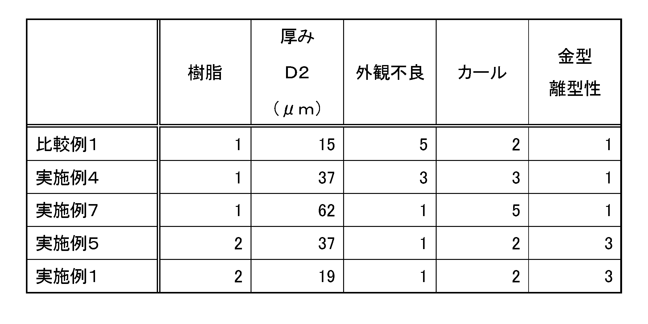
ここで金型離形性は、賦型用金型からの剥離性を評価したものであり、剥離に要する力を5段階により評価した。「1」~「4」は、充分に剥離性を備えており、使用上、何ら問題とならない場合であり、剥離に要する力の大きさにより「1」、「2」、「3」、「4」に分類した。「5」は、剥離に要する力が大きく、剥離に注意を要し、量産に適していない場合である。
この表2によれば、実施例1、5では、硬化収縮が小さい分、厚みD2が小さくても、実施例7と同程度の外観不良の評価結果を得ることができ、またカールが少ないことが判る。また、実施例5は、樹脂1を用いた同じ厚みD2を有する実施例4と比べて、外観不良が向上し、カールも少ないことが判る。しかしながらこのように硬化収縮が小さい場合であっても、充分な金型離形性を確保できることが確認された。
表3は、底部13における硬化物の厚みD2と第1及び第2の壁面K1、K2の算術平均粗さRa等を示す図表である。
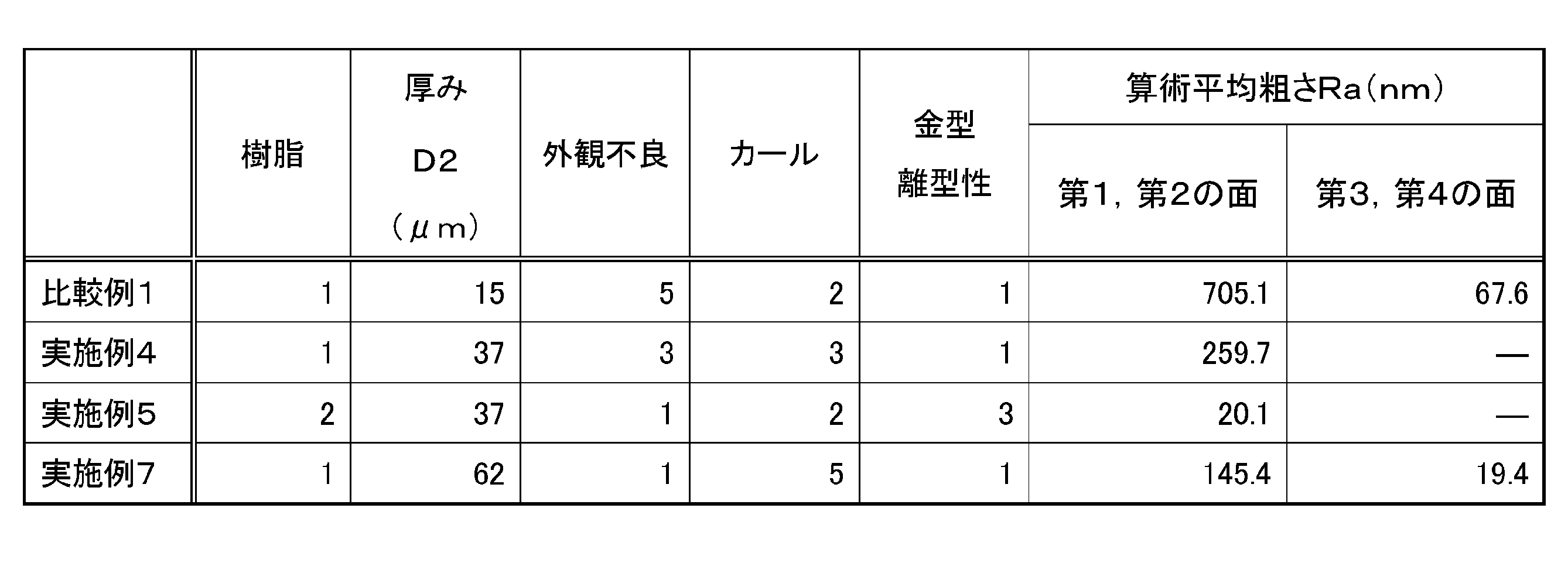
表3に示すように、底部13における硬化物の厚さD2が好ましい範囲を満たしていない比較例1では、第1及び第2の壁面K1、K2の算術平均粗さRaは、その好ましい範囲を大きく超えた値となっていた。これに対して、底部13における硬化物の厚さD2が好ましい範囲を満たす実施例4、5、7では、第1及び第2の壁面K1、K2の算術平均粗さRaは、その好ましい範囲を満たしていた。
これにより、底部13における硬化物の厚さD2が好ましい範囲を満たすことにより、反射面となる第1及び第2の壁面K1、K2の粗面化が緩和されていることが確認できた。第1及び第2の壁面K1、K2の粗面化が緩和されることで、光学素子3の透明性が向上し、外観も良好となる。また、光学素子3により表示される画像を高画質化することができる。
また各例において、凹部9が先細り形状であり、第3及び第4の壁面K3、K4は、基材7の表面に対する鉛直面より深さ方向で凹部9の中心方向に傾いた形状であるため、垂直形状である第1及び第2の壁面K1、K2よりも離型性が良い。そのため、第3及び第4の壁面K3、K4の算術平均粗さRaは、第1及び第2の壁面K1、K2の算術平均粗さRaに比べて抑制される。さらに、実施例7に示すように、底部13における硬化物の厚さD2が好ましい範囲を満たす場合には、第3及び第4の壁面K3、K4の算術平均粗さRaは、より抑制される。これにより、光学素子3の外観や光学性能等をさらに向上させることができる。
これにより、底部13における硬化物の厚さD2が好ましい範囲を満たすことにより、反射面となる第1及び第2の壁面K1、K2の粗面化が緩和されていることが確認できた。第1及び第2の壁面K1、K2の粗面化が緩和されることで、光学素子3の透明性が向上し、外観も良好となる。また、光学素子3により表示される画像を高画質化することができる。
また各例において、凹部9が先細り形状であり、第3及び第4の壁面K3、K4は、基材7の表面に対する鉛直面より深さ方向で凹部9の中心方向に傾いた形状であるため、垂直形状である第1及び第2の壁面K1、K2よりも離型性が良い。そのため、第3及び第4の壁面K3、K4の算術平均粗さRaは、第1及び第2の壁面K1、K2の算術平均粗さRaに比べて抑制される。さらに、実施例7に示すように、底部13における硬化物の厚さD2が好ましい範囲を満たす場合には、第3及び第4の壁面K3、K4の算術平均粗さRaは、より抑制される。これにより、光学素子3の外観や光学性能等をさらに向上させることができる。
またこれら実施例1~実施例8においては、反射面に係る壁面の成す角度等にあっても、上述した範囲を充分に満足することを確認することができた。
この実施形態によれば、凹部の底部に一定の厚みにより硬化性樹脂の硬化物を設けることにより、賦型処理による生産において、硬化収縮による凹部壁面形状の変化を充分に低減することができ、簡易かつ高い精度で量産することができる。
また第1及び第2の壁面に対応する第3及び第4の壁面を備えた四角柱形状により凹部を構成することにより、四角柱形状による凸部をマトリックス状に配置してなる賦型用金型を使用して作製することができ、これにより簡易な構成による賦型用金型を使用して生産性を向上することができる。
また第1及び第2の壁面を算術平均粗さRaを2nm以上260nm以下により作製することができ、表示に供する画像を高画質化することができる。また、第3及び第4の壁面についても、算術平均粗さRaを抑制することができ、表示に供する画像をさらに高画質化することができる。
また繰り返しピッチPを、40μm以上400μm以下、幅W1を20μm以上200μm以下、深さD1を20μm以上600μm以下により凹部を作製することにより、充分に高画質により空間に画像表示する場合にあっても、繰り返しの凹部の底部に、19μm以上150μm以下の厚みにより硬化性樹脂の硬化物を備えることにより、充分に光学素子を簡易に量産することができる。
また凹部の深さD1を、隣接する前記凹部の間隔W2により割り算した比率(D1/W2)が0.05以上30以下である場合に適用して、凹部の底部に19μm以上150μm以下の厚みにより硬化性樹脂の硬化物を備えることにより、アスペクト比が高いことにより硬化収縮による凹部壁面形状の精度劣化が激しい場合に、効果的に、精度を向上することができる。
〔第2実施形態〕
図10は、図2との対比により、第2実施形態に係る光学素子を示す図である。この実施形態では、凹部9に代えて凸部39をマトリックス状に配置してなる凹凸面層38により光学素子33が形成される。
図10は、図2との対比により、第2実施形態に係る光学素子を示す図である。この実施形態では、凹部9に代えて凸部39をマトリックス状に配置してなる凹凸面層38により光学素子33が形成される。
ここでこの凸部39は、第1実施形態に係る光学素子3の表面形状の反転形状による表面形状が形成された賦型用金型により形成される。これにより交差角度90度により交差して反射面を構成する第1及び第2の壁面K1、K2と、この壁面K1、K2にそれぞれ対向するように保持されて、基材7表面の鉛方向に対して斜めに傾いた壁面K3、K4により凸部39が作製される。
光学素子33については、賦型用金型20を使用した第1の賦型処理により、光学素子33の表面形状の反転形状を備えた凹凸面層が形成され、この凹凸面層を使用して生産用の賦型用金型が作製される。またこの生産用の賦型用金型を使用した賦型処理により光学素子33が生産される。
この実施形態では、この反転形状による表面形状に関する構成が異なる点を除いて、第1実施形態と同一に構成される。これにより生産用の賦型用金型を使用した賦型処理においては、凸部39の間に、19μm以上150μm以下の厚みにより硬化性樹脂の硬化物が設けられる。
なお当然に、第1の賦型処理においては、凹部の底部に、19μm以上150μm以下厚みにより硬化性樹脂の硬化物を作製するように実行され、これにより生産用の賦型用金型の作製に供する原版(マザー版)を高い精度で生産できるようにする。
この実施形態では、第1実施形態の反転形状の表面形状により光学素子、周期構造体を作製する場合にあっても、第1の実施形態と同様の効果を得ることができる。
〔第3実施形態〕
この実施形態では、第1実施形態、第2実施形態と同様にして周期構造体を作製し、この周期構造体を空間への画像表示に供する光学素子以外に適用する。具体的には、蛍光等の光学的な反応を検出して微量の試料の分析等を行うバイオチップ等、凸部、凹部をマトリックス状に配置して形成される周期構造体に広く適用することができる。
この実施形態では、第1実施形態、第2実施形態と同様にして周期構造体を作製し、この周期構造体を空間への画像表示に供する光学素子以外に適用する。具体的には、蛍光等の光学的な反応を検出して微量の試料の分析等を行うバイオチップ等、凸部、凹部をマトリックス状に配置して形成される周期構造体に広く適用することができる。
〔他の実施形態〕
以上、本発明の実施に好適な具体的な構成を詳述したが、本発明は、本発明の趣旨を逸脱しない範囲で、上述の実施形態の構成を種々に変更することができる。
以上、本発明の実施に好適な具体的な構成を詳述したが、本発明は、本発明の趣旨を逸脱しない範囲で、上述の実施形態の構成を種々に変更することができる。
1 画像表示装置
2 画像表示パネル
3、33 光学素子
6 リフレクター
8、38 凹凸面層
9 凹部
10 周期構造体
12 壁部
13 底部
20 賦型用金型
20A 賦型処理面
21、39 凸部
22 母材
23 頂部
24 バイト
25 微細溝
K1~K4、L1~L4 壁面
O 物点
Q 像点
RA、RB 反射面
2 画像表示パネル
3、33 光学素子
6 リフレクター
8、38 凹凸面層
9 凹部
10 周期構造体
12 壁部
13 底部
20 賦型用金型
20A 賦型処理面
21、39 凸部
22 母材
23 頂部
24 バイト
25 微細溝
K1~K4、L1~L4 壁面
O 物点
Q 像点
RA、RB 反射面
Claims (14)
- 基材と、
前記基材上に形成された硬化性樹脂の硬化物による凹凸面層とを備え、
前記凹凸面層には、直交する第1及び第2の壁面を備えた凹部が、マトリックス状に配置され、
前記凹部の底部に、19μm以上150μm以下の厚みにより前記硬化性樹脂の硬化物を備えた
光学素子。 - 前記凹部は、
前記第1及び第2の壁面にそれぞれ対向する第3及び第4の壁面を備え、
前記第3及び第4の壁面が、前記基材の表面に対する鉛直面より深さ方向で前記凹部の中心方向に傾いた先細りの形状である
請求項1に記載の光学素子。 - 前記第1及び第2の壁面は、
算術平均粗さRaが2nm以上260nm以下である
請求項1又は請求項2に記載の光学素子。 - 前記凹部の深さは、
前記底部に設けられた前記硬化性樹脂の硬化物の厚みよりも大きい
請求項1から請求項3までの何れかに記載の光学素子。 - 前記底部は、
前記基材の表面に平行であって平坦な平面状である
請求項1から請求項4までの何れかに記載の光学素子。 - 前記凹部は、
繰り返しピッチPが、40μm以上400μm以下であり、
幅W1が20μm以上200μm以下であり、
深さD1が20μm以上600μm以下である
請求項1から請求項5までの何れかに記載の光学素子。 - 前記凹部の深さD1を、隣接する前記凹部の間隔W2により割り算した比率(D1/W2)が0.05以上30以下である
請求項1から請求項6までの何れかに記載の光学素子。 - 基材と、
前記基材上に形成された硬化性樹脂の硬化物による凹凸面層とを備え、
前記凹凸面層には、直交する第1及び第2の壁面を備えた凸部が、マトリックス状に配置され、
隣接する前記凸部の間には、19μm以上150μm以下の厚みにより前記硬化性樹脂の硬化物を備えた
光学素子。 - 基材と、
前記基材上に形成された硬化性樹脂の硬化物による凹凸面層とを備え、
前記凹凸面層には、隣接する第1及び第2の壁面を備えた凹部がマトリックス状に配置され、
前記凹部の底部に、19μm以上150μm以下の厚みにより前記硬化性樹脂の硬化物を備えた
周期構造体。 - 基材と、
前記基材上に形成された硬化性樹脂の硬化物による凹凸面層とを備え、
前記凹凸面層には、隣接する第1及び第2の壁面を備えた凸部がマトリックス状に配置され、
隣接する前記凸部の間には、19μm以上150μm以下の厚みにより前記硬化性樹脂の硬化物を備えた
周期構造体。 - 基材上に、直交する第1及び第2の壁面を備えた凹部が、マトリックス状に配置されてなる凹凸面層が形成された光学素子の製造方法であって、
前記基材に、硬化性樹脂の塗工液を塗工する塗工工程と、
前記凹凸面層の表面形状に対応する表面形状を備えた賦型用金型に、前記硬化性樹脂の塗工液を塗工した基材を押圧して前記硬化性樹脂を硬化させ、前記光学素子の表面形状に対応する表面形状を備えた凹凸面層を作製する硬化工程と、
前記凹凸面層を前記基材と一体に剥離する剥離工程とを備え、
前記塗工工程では、
前記凹部の底部に、19μm以上150μm以下の厚みにより前記硬化性樹脂の硬化物を作製する厚みにより前記硬化性樹脂の塗工液を塗工する
光学素子の製造方法。 - 基材上に、直交する第1及び第2の壁面を備えた凸部が、マトリックス状に配置されてなる凹凸面層が形成された光学素子の製造方法において、
前記基材に、硬化性樹脂の塗工液を塗工する塗工工程と、
前記凹凸面層の表面形状に対応する表面形状を備えた賦型用金型に、前記硬化性樹脂の塗工液を塗工した基材を押圧して前記硬化性樹脂を硬化させ、前記光学素子の表面形状に対応する表面形状を備えた凹凸面層を作製する硬化工程と、
前記凹凸面層を前記基材と一体に剥離する剥離工程とを備え、
前記塗工工程では、
隣接する前記凸部の間に、19μm以上150μm以下の厚みにより前記硬化性樹脂の硬化物を作製する厚みにより前記硬化性樹脂の塗工液を塗工する
光学素子の製造方法。 - 基材上に、隣接する第1及び第2の壁面を備えた凹部がマトリックス状に配置されてなる凹凸面層が形成された周期構造体の製造方法であって、
前記基材に、硬化性樹脂の塗工液を塗工する塗工工程と、
前記凹凸面層の表面形状に対応する表面形状を備えた賦型用金型に、前記硬化性樹脂の塗工液を塗工した基材を押圧して前記硬化性樹脂を硬化させ、前記賦型用金型の表面形状に対応する表面形状を備えた凹凸面層を作製する硬化工程と、
前記凹凸面層を前記基材と一体に剥離する剥離工程とを備え、
前記塗工工程では、
前記凹部の底部に、19μm以上150μm以下の厚みにより前記硬化性樹脂の硬化物を作製する厚みにより前記硬化性樹脂の塗工液を塗工する
周期構造体の製造方法。 - 基材上に、隣接する第1及び第2の壁面を備えた凸部がマトリックス状に配置されてなる凹凸面層が形成された周期構造体の製造方法において、
前記基材に、硬化性樹脂の塗工液を塗工する塗工工程と、
前記凹凸面層の表面形状に対応する表面形状を備えた賦型用金型に、前記硬化性樹脂の塗工液を塗工した基材を押圧して前記硬化性樹脂を硬化させ、前記賦型用金型の表面形状に対応する表面形状を備えた凹凸面層を作製する硬化工程と、
前記凹凸面層を前記基材と一体に剥離する剥離工程とを備え、
前記塗工工程では、
隣接する前記凸部の間に、19μm以上150μm以下の厚みにより前記硬化性樹脂の硬化物を作製する厚みにより前記硬化性樹脂の塗工液を塗工する
周期構造体の製造方法。
Applications Claiming Priority (4)
| Application Number | Priority Date | Filing Date | Title |
|---|---|---|---|
| JP2016-070149 | 2016-03-31 | ||
| JP2016070149 | 2016-03-31 | ||
| JP2017-062321 | 2017-03-28 | ||
| JP2017062321A JP6780560B2 (ja) | 2016-03-31 | 2017-03-28 | 光学素子、周期構造体 |
Publications (1)
| Publication Number | Publication Date |
|---|---|
| WO2017170744A1 true WO2017170744A1 (ja) | 2017-10-05 |
Family
ID=59964624
Family Applications (1)
| Application Number | Title | Priority Date | Filing Date |
|---|---|---|---|
| PCT/JP2017/013021 Ceased WO2017170744A1 (ja) | 2016-03-31 | 2017-03-29 | 光学素子、周期構造体、光学素子の製造方法及び周期構造体の製造方法 |
Country Status (1)
| Country | Link |
|---|---|
| WO (1) | WO2017170744A1 (ja) |
Cited By (1)
| Publication number | Priority date | Publication date | Assignee | Title |
|---|---|---|---|---|
| JP2019139023A (ja) * | 2018-02-08 | 2019-08-22 | 株式会社パリティ・イノベーションズ | 光学素子及びそれを用いた映像表示装置 |
Citations (6)
| Publication number | Priority date | Publication date | Assignee | Title |
|---|---|---|---|---|
| WO2007116639A1 (ja) * | 2006-03-23 | 2007-10-18 | National Institute Of Information And Communications Technology | 結像素子、ディスプレイ装置 |
| JP2008158114A (ja) * | 2006-12-21 | 2008-07-10 | National Institute Of Information & Communication Technology | 光学システム |
| WO2009041646A1 (ja) * | 2007-09-28 | 2009-04-02 | Asahi Glass Company, Limited | 光硬化性組成物、微細パターン形成体の製造方法および光学素子 |
| WO2011108469A1 (ja) * | 2010-03-01 | 2011-09-09 | シャープ株式会社 | 反射型結像素子および光学システム |
| JP2014016576A (ja) * | 2012-07-11 | 2014-01-30 | Nitto Denko Corp | マイクロミラーアレイおよびその製法 |
| JP2014228674A (ja) * | 2013-05-22 | 2014-12-08 | セイコーエプソン株式会社 | 回折光学素子、回折光学素子の製造方法、及び電子機器 |
-
2017
- 2017-03-29 WO PCT/JP2017/013021 patent/WO2017170744A1/ja not_active Ceased
Patent Citations (6)
| Publication number | Priority date | Publication date | Assignee | Title |
|---|---|---|---|---|
| WO2007116639A1 (ja) * | 2006-03-23 | 2007-10-18 | National Institute Of Information And Communications Technology | 結像素子、ディスプレイ装置 |
| JP2008158114A (ja) * | 2006-12-21 | 2008-07-10 | National Institute Of Information & Communication Technology | 光学システム |
| WO2009041646A1 (ja) * | 2007-09-28 | 2009-04-02 | Asahi Glass Company, Limited | 光硬化性組成物、微細パターン形成体の製造方法および光学素子 |
| WO2011108469A1 (ja) * | 2010-03-01 | 2011-09-09 | シャープ株式会社 | 反射型結像素子および光学システム |
| JP2014016576A (ja) * | 2012-07-11 | 2014-01-30 | Nitto Denko Corp | マイクロミラーアレイおよびその製法 |
| JP2014228674A (ja) * | 2013-05-22 | 2014-12-08 | セイコーエプソン株式会社 | 回折光学素子、回折光学素子の製造方法、及び電子機器 |
Cited By (1)
| Publication number | Priority date | Publication date | Assignee | Title |
|---|---|---|---|---|
| JP2019139023A (ja) * | 2018-02-08 | 2019-08-22 | 株式会社パリティ・イノベーションズ | 光学素子及びそれを用いた映像表示装置 |
Similar Documents
| Publication | Publication Date | Title |
|---|---|---|
| RU2010108321A (ru) | Оптическая пленка и способ ее изготовления, противобликовый поляризатор и устройство отображения | |
| US8638511B2 (en) | Reflector array optical device and display device using the same | |
| CN104937448B (zh) | 具备平行配置的光反射部的光控制面板的制造方法 | |
| CN1894605A (zh) | 改变光线方向的光学结构及其成形工艺 | |
| WO2013113295A1 (zh) | 增光膜 | |
| JP6885877B2 (ja) | グレーデッド拡散体 | |
| WO2013058230A1 (ja) | リフレクタアレイ光学装置及びその作製方法 | |
| CN116594090A (zh) | 一种可视角度控制膜及其制备方法 | |
| TWI611218B (zh) | 一種光學擴散膜片製作方法 | |
| JP6780560B2 (ja) | 光学素子、周期構造体 | |
| WO2017170744A1 (ja) | 光学素子、周期構造体、光学素子の製造方法及び周期構造体の製造方法 | |
| WO2019021497A1 (ja) | 立体像結像装置及びその製造方法 | |
| JP5724527B2 (ja) | 導光板積層体およびその製造方法 | |
| JP6274102B2 (ja) | 光拡散性シート | |
| JP2018014307A (ja) | 表示装置用照明ユニットおよび表示装置 | |
| CN115079504A (zh) | 微结构投影幕布及其制备方法 | |
| WO2020118962A1 (zh) | 一种背板组件用反光贴条及其制备方法 | |
| JP6265018B2 (ja) | 照明用光学シートおよびそれを用いた照明装置 | |
| CN102879855A (zh) | 导光板及其制造方法 | |
| CN101685167A (zh) | 镀膜治具 | |
| US12411356B2 (en) | Aerial image forming element comprising a transparent base member having first and second reflecting surfaces and aerial image forming device | |
| KR20200008545A (ko) | 반사 방지 부재 | |
| CN109471327A (zh) | 一种s形抗光幕布及其制备方法 | |
| CN107907927B (zh) | 一种三棱镜结构及其制备方法、及一种三棱镜阵列 | |
| JP6293990B2 (ja) | 光学フィルム、光学フィルム用転写体、画像表示装置及び光学フィルムの製造用金型 |
Legal Events
| Date | Code | Title | Description |
|---|---|---|---|
| NENP | Non-entry into the national phase |
Ref country code: DE |
|
| 121 | Ep: the epo has been informed by wipo that ep was designated in this application |
Ref document number: 17775278 Country of ref document: EP Kind code of ref document: A1 |
|
| 122 | Ep: pct application non-entry in european phase |
Ref document number: 17775278 Country of ref document: EP Kind code of ref document: A1 |