WO2017170457A1 - 圧力センサ - Google Patents
圧力センサ Download PDFInfo
- Publication number
- WO2017170457A1 WO2017170457A1 PCT/JP2017/012493 JP2017012493W WO2017170457A1 WO 2017170457 A1 WO2017170457 A1 WO 2017170457A1 JP 2017012493 W JP2017012493 W JP 2017012493W WO 2017170457 A1 WO2017170457 A1 WO 2017170457A1
- Authority
- WO
- WIPO (PCT)
- Prior art keywords
- diaphragm
- die
- circuit
- pressure sensor
- microphone
- Prior art date
- Legal status (The legal status is an assumption and is not a legal conclusion. Google has not performed a legal analysis and makes no representation as to the accuracy of the status listed.)
- Ceased
Links
Images


Classifications
-
- H—ELECTRICITY
- H04—ELECTRIC COMMUNICATION TECHNIQUE
- H04R—LOUDSPEAKERS, MICROPHONES, GRAMOPHONE PICK-UPS OR LIKE ACOUSTIC ELECTROMECHANICAL TRANSDUCERS; ELECTRIC HEARING AIDS; PUBLIC ADDRESS SYSTEMS
- H04R19/00—Electrostatic transducers
- H04R19/04—Microphones
-
- H—ELECTRICITY
- H10—SEMICONDUCTOR DEVICES; ELECTRIC SOLID-STATE DEVICES NOT OTHERWISE PROVIDED FOR
- H10D—INORGANIC ELECTRIC SEMICONDUCTOR DEVICES
- H10D48/00—Individual devices not covered by groups H10D1/00 - H10D44/00
- H10D48/50—Devices controlled by mechanical forces, e.g. pressure
Definitions
- the present invention relates to a high-performance pressure sensor.
- the pressure sensor is used as, for example, a microphone that measures diaphragm vibration due to a change in air pressure.
- ECM Electret Condenser Microphone
- MEMS Micro Electro Mechanical Systems
- MEMS microphones are widely used in mobile phones, smartphones, tablet computers and the like because of their small size and low cost, and excellent shock resistance and acoustic phase characteristics. In many cases, a plurality of MEMS microphones are mounted for noise canceling.
- electrostatic type includes a back chamber, a back plate (counter electrode), and a sensing diaphragm. The capacitance changes according to a change in the distance between the back plate and the diaphragm. Or it is converted into a change in frequency.
- the back plate is provided with a number of holes (perforation holes) through which air passes.
- Microphone performance indicators include sensitivity, signal / noise ratio (SNR), maximum sound pressure level, dynamic range, directivity, frequency characteristics, power consumption, etc.
- SNR is an indicator that shows how small the sound can be picked up. is there.
- the SNR of a MEMS microphone is about 65 dB.
- a MEMS microphone having a higher SNR is required.
- Non-Patent Document 1 Non-Patent Document 1
- Non-Patent Document 2 Non-Patent Document 2
- Non-Patent Document 2 Non-Patent Document 2
- ASIC diaphragm displacement readout circuit
- Non-Patent Document 6 An organic / inorganic hybrid structure that cannot be used and can be formed at a low temperature is used. In view of the mechanical properties of the diaphragm, this material is undesirable compared to polysilicon.
- Non-patent Document 7 another method is to form a circuit so that it can withstand the polysilicon deposition temperature (Non-patent Document 7), and such a method of manufacturing an integrated MEMS has been widely applied to inertial sensors.
- a special circuit has to be used, which is deceived from the viewpoint of performance and cost.
- Noise includes electrical noise and mechanical noise.
- the former is lowered by integrating the MEMS structure and the readout circuit.
- the majority of the latter is fluid noise generated when the air flow is restricted by a hole (perforation hole) formed in the back plate. Therefore, a structure that does not require a back plate is desirable to reduce mechanical noise.
- Non-Patent Document 9 a method of reading out capacitance using a comb electrode provided around the diaphragm (Patent Documents 3 and 4), a piezoelectric type (Patent Documents 5 and 6, Non-Patent Document 8), and a piezoresistor A method of making a mold (Non-Patent Document 9) is known.
- Non-Patent Documents 1, 3 and 4 the diaphragm and the displacement reading circuit (ASIC) of the diaphragm are formed on separate dies and connected by wiring by wire bonding or the like. Therefore, the displacement of the diaphragm is detected by the reading circuit. Can be read. However, if the displacement of the diaphragm is minute, the signal in the readout circuit becomes minute, so that the SNR deteriorates. On the other hand, in order to improve the SNR, it is better that the capacitance between the diaphragm and the back plate is as close as possible to the readout circuit, so that the diaphragm and all necessary circuits including the readout circuit are formed on the same die. There is an integrated MEMS microphone.
- the following two methods are conceivable for manufacturing the diaphragm and the circuit on the same die.
- a method of forming a diaphragm on a wafer on which a circuit is formed by a current standard semiconductor process As described above, after forming a circuit, it is necessary to form a diaphragm by using a material and a process that do not damage the circuit. This is possible by using a resin film or a metal thin film, but the area corresponding to the diaphragm portion is reduced. It must be left on the wafer during circuit formation. In the current standard semiconductor process, since the added value per unit area on the wafer is high, such a method is disadvantageous in cost.
- the diaphragm is formed of proven polysilicon, and a special circuit that can withstand the formation of polysilicon requiring high temperature is formed on the wafer.
- a semiconductor process for a special circuit that is, a special production line must be prepared, and this method is economically difficult in view of the maintenance and maintenance costs of the semiconductor line.
- the above-mentioned special circuit cannot be miniaturized, and is extremely disadvantageous in terms of performance and miniaturization.
- the conventional microphone configuration has disadvantages such as an increase in size, an increase in cost, and a compromise in performance. Without it, it is difficult to realize.
- a problem with a microphone also applies to a pressure sensor such as an atmospheric pressure sensor or an ultrasonic sensor.
- an object of the present invention is to provide a small pressure sensor having high performance characteristics at low cost.
- the present invention has the following concept.
- one or more diaphragms A counter electrode provided to face the diaphragm;
- An input circuit that receives the vibration signal of the diaphragm and converts the capacitance of the diaphragm and the counter electrode into a signal of voltage, current, or frequency;
- a signal processing circuit that performs analog processing, digital processing, or both of the signal from the input circuit; and
- the diaphragm and the input circuit are provided in a first die;
- the signal processing circuit is provided in a second die;
- the pressure sensor wherein the first die and the second die are connected by wiring.
- the first die includes an input circuit that receives the diaphragm and the diaphragm vibration signal, and converts the capacitance of the diaphragm and the counter electrode into a signal of voltage, current, or frequency
- the two dies are provided with a signal processing circuit that performs either or both of analog processing and digital processing on a signal from the input circuit, and the first die and the second die are connected by wiring. Therefore, the vibration signal of the diaphragm is input to the input circuit on the same die, and the electric signal converted by the input circuit is input to the signal processing circuit on the second die via the wiring such as the bond wire.
- the configuration of the present invention in which the diaphragm and the first stage input circuit are formed on the same die can increase the SNR. Furthermore, a high SNR can be realized at a low cost for the reasons described below.
- the input circuit integrated on the first die does not necessarily have to be manufactured by an advanced semiconductor process.
- an old generation semiconductor line that is not suitable for manufacturing a fine integrated circuit may be used. This is because the input circuit of the first stage does not deteriorate in performance or the circuit portion becomes too large even if an old generation semiconductor process (for example, design rule 0.35 ⁇ m) is used.
- an old generation semiconductor process for example, design rule 0.35 ⁇ m
- the diaphragm and the circuit are formed on the same wafer, the material and process of the diaphragm must not damage the circuit, and the metallic glass thin film is one of the promising materials.
- the first-stage input circuit can be designed to withstand the diaphragm formation process, and for example, the circuit or a part thereof can be prepared before forming the polysilicon diaphragm. It is.
- the circuit formed on the second die in particular the digital circuit, is more advantageous in terms of performance, miniaturization, and power saving when manufactured by a semiconductor process with a more advanced generation. Since the second die can be outsourced to a so-called CMOS founder as standard, it is economically advantageous.
- a compact pressure sensor having high performance characteristics can be provided at low cost.
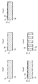
- FIG. 1 shows the structure of the pressure sensor which concerns on embodiment of this invention. It is a block diagram of the pressure sensor which concerns on embodiment of this invention different from FIG. It is a figure which shows the structure of the diaphragm part of the microphone as a pressure sensor which concerns on embodiment of this invention. It is a figure which shows the diaphragm which comprises the microphone as a pressure sensor which concerns on embodiment of this invention, and shows a top view in an upper stage, and shows sectional drawing in a lower stage. Step 1 relating to the method of manufacturing a microphone according to the embodiment of the present invention is shown, and a plan view is shown in the upper part and a sectional view is shown in the lower part.
- Step 2 relating to the microphone manufacturing method according to the embodiment of the present invention is shown, and a plan view is shown in the upper part and a sectional view is shown in the lower part.
- Step 3 relating to the microphone manufacturing method according to the embodiment of the present invention is shown, and a plan view is shown in the upper part and a sectional view is shown in the lower part.
- Step 4 regarding the method for manufacturing a microphone according to the embodiment of the present invention is shown, and a plan view is shown in the upper part and a sectional view is shown in the lower part.
- Step 5 relating to the method of manufacturing a microphone according to the embodiment of the present invention is shown, and a plan view is shown in the upper part and a sectional view is shown in the lower part.
- Step 6 relating to the method of manufacturing a microphone according to the embodiment of the present invention is shown, and a plan view is shown in the upper part and a sectional view is shown in the lower part.
- Step 7 relating to the microphone manufacturing method according to the embodiment of the present invention is shown, and a plan view is shown in the upper part and a sectional view is shown in the lower part.
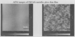
- It is an AFM image of PdCuSi metallic glass regarding an Example.
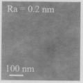
- It is an AFM image of ZrCuAlNi metallic glass regarding an Example.
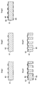
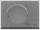
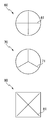
- FIG. 9 is a diagram showing a method of manufacturing a metallic glass diaphragm different from FIG. It is a SEM image of the diaphragm produced in the Example. It is a figure which shows the variation of the shape of a diaphragm.
- the pressure sensor is a microphone.
- the illustrated embodiment is one of the best modes for carrying out the present invention, and includes modifications appropriately made within the scope of the present invention.
- the present invention can be applied not only to the case where the pressure sensor is a microphone but also to the case of an atmospheric pressure sensor or an ultrasonic sensor.
- FIG. 1 is a diagram showing a configuration of a pressure sensor according to an embodiment of the present invention.
- the pressure sensor 100 of the present invention is configured by mounting a first die 102 and a second die 103 on a base 101 of a package.
- the first die 102 includes a diaphragm 104 made of metal glass having a MEMS structure, a counter electrode 105, and a readout circuit 106, and the diaphragm 104, the counter electrode 105, and the readout circuit 106 are connected by wiring (not shown) on the die.
- the counter electrode 105 has a plurality of perforation holes.
- the readout circuit 106 includes an input circuit 106a.
- the input circuit 106a receives a diaphragm vibration signal and converts the electrostatic capacitance of the diaphragm 104 and the counter electrode 105 into a signal of voltage, current, or frequency.
- the input circuit 106a may further include an amplifier. Amplification, modulation, impedance conversion, or the like may be performed after conversion to a voltage, current, or frequency signal.
- Examples of the input circuit 106a include a first stage amplifier such as a transimpedance amplifier and a capacitance-frequency conversion circuit such as a Schmitt trigger.
- the second die 103 includes a signal processing circuit (integrated circuit) 107 that performs analog processing, digital processing, or both.
- the first die 102 and the second die 103 are arranged side by side on the same surface.
- the input circuit 106a on the first die 102 and the signal processing circuit 107 on the second die 103 are connected to the base 101 by wiring 108 such as wire bonding.
- the signal processing circuit 107 receives the signal converted by the input circuit 106a. For example, a signal that has been voltage-converted and amplified by the first-stage amplifier of the input circuit 106a on the first die 102 or a frequency signal that has been frequency-converted by the capacitance-frequency conversion circuit is sent to the first die by the wire bonding wiring 108. It can be easily removed out of 102 and then processed by circuitry 107 on the second die 103.
- any one of various circuits such as a first stage amplifier and a capacitance-frequency conversion circuit is integrated with the diaphragm 104 as the input circuit 106a, the effects of noise reduction and dynamic range expansion can be obtained without integrating all the circuits. It is done.
- the signal processing circuit 107 on the second die 103 includes a digital signal processing circuit
- a circuit including the first-stage analog portion is formed on the first die 102 having the diaphragm 104, and the subsequent circuits are formed on the second die 103, which is another die, with another semiconductor process rule (minimum semiconductor wiring width). Then, they are connected by the wiring 108.
- the process rule of the circuit on the first die 102 of the integrated microphone is different from the process rule of the circuit formed on the second die 103, more specifically, the latter process rule. Is made smaller than the former process rule.
- the first die 102 of the microphone is formed with rules of 0.35 ⁇ m and 0.18 ⁇ m, for example, and the second die 103 to be a chip of a digital circuit is formed with rules of 0.14 ⁇ m and 90 nm of 0.18 ⁇ m or less, for example. It is formed. Also, the size of the wafer on which the microphone and the digital circuit are respectively manufactured is different.
- the microphone is manufactured on an 8-inch wafer, and the chip of the digital circuit is manufactured on a 12-inch wafer.
- the process rule of the circuit provided in the second die 103 is smaller than the process rule of the circuit provided in the first die 102.
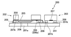
- FIG. 2 is a diagram showing a configuration of a pressure sensor according to an embodiment of the present invention different from FIG.
- the pressure sensor 200 is configured by mounting a first die 202 and a second die 203 on a base 201 of a package.
- the first die 202 includes a metallic glass diaphragm 204 having a MEMS structure, a counter electrode 205, and a readout circuit 206, and the diaphragm 204, the counter electrode 205, and the readout circuit 206 are connected by wiring (not shown) on the die. Yes.
- the counter electrode 205 has a plurality of perforation holes.
- the read circuit 206 includes an input circuit 206a.
- the input circuit 206a receives the vibration signal of the diaphragm 204, and converts the electrostatic capacitance between the diaphragm 204 and the counter electrode 205 into a voltage, current, or frequency signal.
- the input circuit 206a may further include an amplifier. Amplification, modulation, impedance conversion, or the like may be performed after conversion to a voltage, current, or frequency signal.
- Examples of the input circuit 206a include a first stage amplifier such as a transimpedance amplifier and a capacitance-frequency conversion circuit such as a Schmitt trigger.
- the second die 203 includes a signal processing circuit (integrated circuit) 207 that performs one or both of analog processing and digital processing.
- the base 201 includes a sound hole 201a, and the wiring 201b is formed on the base 201 so as to have a pattern, and the bump 208 is mounted on the wiring 201b.
- the bumps 208 are connected to the diaphragm 204, the readout circuit 206, and the signal processing circuit 207.
- a voltage signal that has been voltage-converted and amplified by the first-stage amplifier of the input circuit 206a on the first die 202 or a frequency signal that has been frequency-converted by the capacitance-frequency converter circuit. Can be easily taken out of the first die 202 by the bump 208 and the wiring 201b, and then processed by the signal processing circuit 207 on the second die 203. If necessary, the gap between the base 201 of the package and the first die 202 is sealed with a sealing material 209 such as a resin so that the sound pressure does not leak.
- the vibration signal of the diaphragm 204 is input to the input circuit 206a in the readout circuit 206, and is converted into a voltage-converted and amplified signal or a frequency-converted frequency signal by the input circuit 206a.
- the signal is input from the input circuit 206a to the signal processing circuit 207 of the second die 203 via the bump 208, the wiring 201b, and the bump 208.
- the diaphragms 104 and 204 are not limited as long as they are made of materials and processes that do not damage the readout circuits 106 and 206.
- the diaphragm is a metal glass
- the diaphragm made of metal glass is soft and easily deformed, it is easily deformed by pressure and can maintain mechanical strength.
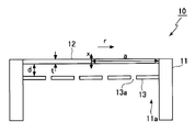
- FIG. 3 is a diagram showing a configuration of a diaphragm portion of a microphone as a pressure sensor according to an embodiment of the present invention.
- the microphone 10 according to the embodiment of the present invention includes a cylindrical support frame 11 and a diaphragm 12 made of metal glass and a counter electrode 13.
- the support frame 11 includes a cavity 11a
- the counter electrode 13 includes a plurality of perforation holes 13a.
- the diaphragm 12 and the counter electrode 13 are opposed to each other, and the displacement due to the sound pressure of the diaphragm 12 is measured as a capacitance and converted into a voltage by a reading circuit (not shown).
- the diaphragm 12 is made of a metallic glass film.
- the sensitivity is improved by forming the diaphragm with metal glass.
- Equation 1 The capacitance C of the gap d formed by the diaphragm 12 having the area A and the counter electrode 13 is described by Equation 1 where ⁇ o is the dielectric constant of air.
- V DC DC voltage
- the interval d is reduced by x DC due to the electrostatic force
- the capacitance C 0 at that time is described by Equation 2.
- the charge Q DC accumulated at that time is described by Equation 3.
- the displacement x of the diaphragm 12 is described in Equation 4,
- the resulting voltage VAC is described by Equation 5.
- the output current of the microphone 10 when the impedance Z I represented by the current I AC of formula 6.
- the deformation when the pressure P is applied to the diaphragm 12 can be estimated by an equation of material mechanics, and the displacement x (r) at the position r from the center is expressed by a and t, respectively, the radius and thickness of the diaphragm 12.
- D is the bending rigidity of the diaphragm 12 and is described by Equation 8.
- E is the Young's modulus of the material of the diaphragm 12, and ⁇ is the Poisson's ratio of the material of the diaphragm 12.
- the average displacement x is obtained by Equation 9.
- Equation 10 the relationship shown in Equation 10 is obtained from Equation 6 and Equation 9. From this equation, it can be seen that if the dimensions are the same, the output current is approximately inversely proportional to the Young's modulus E of the material of the diaphragm 12. That is, the sensitivity is approximately inversely proportional to the Young's modulus E of the material of the diaphragm 12.
- Table 1 compares the relative sensitivity of the microphones when the material of the diaphragm 12 is polysilicon and PdSiCu and ZrCuAlNi are used as the metallic glass.
- Polysilicon data (*) is cited from Non-Patent Document 9.
- Data on metallic glass (**) is cited from Non-Patent Document 10.
- Metallic glass has a tensile strength equal to or higher than that of polysilicon. More importantly, metallic glass is a ductile material and is less likely to break due to impact or stress concentration than polysilicon, which is a brittle material. Therefore, by changing the material of the diaphragm 12 from polysilicon to metal glass, the diaphragm 12 can be made thin while maintaining reliability. Or if it is the same diaphragm thickness, reliability can be made high.
- Equation 13 The ratio of the resonance frequency of the polysilicon diaphragm to the metallic glass diaphragm is expressed by Equation 13.
- Table 3 shows the density, relative sensitivity ((1- ⁇ 2 ) / E), and resonance frequency ratio for PdSiCu and ZrCuAlNi as polysilicon and metallic glass.
- the data (**) of metallic glass are cited from Non-Patent Document 10.
- the diameter 0 If the magnification is 39 times, approximately the same resonance frequency and breakdown voltage can be obtained. At this time, the relative sensitivity is substantially the same (1.03 times) compared with that made of polysilicon. On the other hand, the area of the diaphragm is approximately 0.15 times, and the die can be significantly reduced in size while maintaining sensitivity.
- the diaphragm is significantly reduced, so that it is possible to mount a plurality of diaphragms on the same die, but it is also possible to arrange M rows ⁇ N columns of diaphragms on the same die in a matrix.
- M rows ⁇ N columns of diaphragms on the same die in a matrix.
- the area of the die increases only by about 20%, but the sensitivity is improved by 8 times or more.
- a phased array can be configured using a plurality of diaphragms, and the distance and direction of an object by ultrasonic waves can be measured.
- the thickness of the diaphragm is changed in the diaphragm, for example, a thick portion is arranged in a honeycomb shape, a lattice shape, a radial shape, a concentric shape, or a combination thereof, and the resonance frequency and the mechanical strength. Sensitivity can be improved while maintaining high.
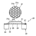
- FIG. 4 is a diagram showing a diaphragm 21 constituting the microphone 20 according to the embodiment of the present invention, in which a plan view is shown in the upper part and a sectional view is shown in the lower part.
- the microphone 20 includes a MEMS die 22, a substrate 24 having a cavity 23, a counter electrode 26 having a plurality of perforation holes 25 on the substrate 24, and a diaphragm 21, and at least the diaphragm 21 and the counter electrode 26 are insulated.
- a reading circuit 27 is mounted on the substrate 24.
- the diaphragm 21 has a thick portion 21a arranged in a honeycomb shape, and defines a thin portion 21b.
- the perforation hole 25 and the thick portion 21 a may be opposed to each other, or the thick portion may be formed on the opposite side of the diaphragm 21. Thereby, even if the diaphragm 21 is formed of metal glass, the strength can be surely provided.
- the rigidity of the diaphragm and the resonance frequency related to it change depending on the stress of the diaphragm. Therefore, stress is one of the parameters that control the characteristics of the diaphragm.
- One of the methods for solving the above-mentioned problem of lowering the resonance frequency is a method of pulling the stress of the diaphragm so that the resonance frequency in the diaphragm made of metallic glass is comparable to the resonance frequency in the diaphragm made of Si. is there.
- the resonance frequency is increased by pulling the diaphragm, a tensile stress of 0 to 500 MPa is preferable.
- the diaphragm is easily broken by setting the tensile stress, the tensile stress in this range can be solved by the excellent mechanical properties of the metal glass.
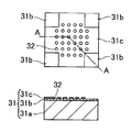
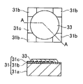
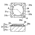
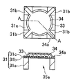
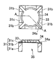
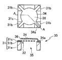
- 5A to 5G are views showing a method for manufacturing the microphone 30 according to the embodiment of the present invention.
- 5A to 5G a plan view is shown in the upper stage, and a cross-sectional view along the line AA is shown in the lower stage. Note that the reading circuit is not shown.
- a substrate 31 having a layer (referred to as “counter electrode layer”) 31 c to be a counter electrode is prepared.
- a reading circuit (not shown) is prepared in advance on the substrate 31.
- an SOI substrate 31 having a SiO2 layer 31b on a Si substrate 31a and a Si semiconductor layer 31c on the SiO2 layer 31b is prepared.
- a plurality of holes (perforation holes) 32 are provided in the counter electrode layer 31c.
- a plurality of holes (perforation holes) 32 are provided in the Si semiconductor layer 31c on the surface of the SOI substrate 31 by etching. Further, each corner portion of the Si semiconductor layer 31c is etched into a rectangular shape to expose the SiO2 layer 31b. At this time, a reading circuit (not shown) is protected by a photoresist.
- the hole 32 is filled and a sacrificial layer 33 is provided on the counter electrode layer 31c. Specifically, as shown in FIG.
- the hole 32 is filled and a sacrificial layer 33 of resin (photoresist) is provided on the Si semiconductor layer 31c. If necessary, the surface of the resin is flattened by reflow.
- metal glass is provided in a layered manner on part of the counter electrode layer 31c and the sacrificial layer 33. Specifically, as shown in FIG. 5D, a metallic glass layer 34 is provided on a part of the Si semiconductor layer 31 c and the sacrificial layer 33.
- the metallic glass is formed by sputtering and patterned by etching using a photoresist as a mask. Metal glass on the reading circuit (not shown) is also removed.
- a part of the metallic glass layer 34 is provided on the SiO2 layer 31b and becomes a support portion 34a.
- a photoresist is patterned on the existing metallic glass, and the metallic glass is formed thereon by sputtering and lifted off.
- the diaphragm, the counter electrode, and the reading circuit are connected by a thin film wiring (not shown), and the counter electrode, the sacrificial layer 33, and the metal glass layer 24 are released from the substrate 31 by etching the back surface of the substrate 31.
- Step 5 as shown in FIG.
- a part of the Si substrate 31a on the back side of the SOI substrate 31 is removed by etching to constitute a part 35a of the cavity.
- Step 6 as shown in FIG. 5F, the substrate 31 is removed up to the back surface side of the Si semiconductor layer 31c, and the cavity 35 is formed.
- Step 7 as shown in FIG. 5G, the sacrificial layer 33 is removed by oxygen ashing, etching with an organic solvent, or atomic hydrogen etching, and the diaphragm 36 is released.
- the sacrificial layer 33 is removed by oxygen ashing, etching with an organic solvent, or atomic hydrogen etching, and the diaphragm 36 is released.
- the circuit can be easily integrated on the microphone. It is easy to form wiring between the reading circuit and the diaphragm 36 prepared in advance and wiring with the second die.
- Zr-based metal glass As the metal glass, the case of PdSiCu and ZrCuAlNi has been described as an example, but Zr-based metal glass, Pd-based metal glass, Pt-based metal glass, Au-based metal glass, Fe-based metal glass, Ni-based metal glass, Any of Mg-based metallic glass, Co-based metallic glass, and Cu-based metallic glass may be used.
- Zr-based metallic glass there are Zr 53 Ti 5 Cu 20 Ni 12 Al 10 , Zr 55 Cu 30 Al 10 Ni 5 , Zr 75 Cu 19 Al 6, etc.
- Examples of Pd-based metallic glass include Pd 40 Ni 10 Cu 30 P 20 , Pd 78 Cu 6 Si 16 , Examples of Pt-based metallic glass include Pt 58 Cu 15 Ni 5 P 23 , Au-based metallic glass includes Au 49 Ag 6 Pd 2 Cu 27 Si 16 Examples of Fe-based metallic glass include Fe 76 Si 9 B 10 P 5 . Examples of Ni-based metallic glass include Ni 60 Nb 15 Ti 20 Zr 5 and the like. Examples of the Mg-based metallic glass include Mg 57 Cu 34 Nd 9 and Mg 64 Ni 21 Nd 15 . Examples of the Co-based metallic glass include Co 56 Ta 9 B 35 . Examples of the Cu-based metallic glass include Cu 50 Zr 50 and Cu 50 Zr 45 A 15 . These metallic glasses can be formed into a film by a sputtering method.
- the metal glass may have Zr as a main element. This is because the tensile strength is high, the density is small, and the mechanical properties are not only excellent, but also the raw material can be obtained at a lower cost than the metal glass mainly composed of Pd, Au, and Pt, and the manufacturing cost is reduced. In addition, since there is no magnetism, it is not affected by magnetic noise. Co-based metallic glass and Cu-based metallic glass have a large strength (specific strength) with respect to density, and the former is particularly large.
- PdCuSi and ZrCuAlNi were selected as new materials for the MEMS microphone.
- a metallic glass film can be deposited by a sputtering method, it is not common as a MEMS material, and film stress control is not easy, and the film stress is precisely controlled from zero stress to an appropriate tensile stress.
- the present inventors conducted basic studies and found that metallic glass formed by a sputtering method can be applied to a MEMS microphone.
- PdCuSi metallic glass was deposited by sputtering under the following conditions.
- the high frequency power was 100 W
- the Ar gas flow rate was 10 sccm
- the deposition pressure was 1.34 Pa
- the deposition time was 50 minutes
- one cycle was 300 seconds
- the cool-down time was 300 seconds.
- the rotation speed of the substrate was 20 rpm.
- the deposition rate of PdCuSi metallic glass was 16.6 nm / min. Thereafter, annealing was performed at 350 ° C. to 410 ° C., and the film stress was adjusted to the above range.
- FIG. 6 is an AFM image of PdCuSi metallic glass. From this image, it was found that the surface roughness Ra was about 0.1 nm, and a sufficiently smooth metallic glass thin film was formed.
- ZrCuAlNi metallic glass was deposited by sputtering under the following conditions.
- the high frequency power was 100 W
- the Ar gas flow rate was 15 sccm
- the deposition pressure was 0.4 Pa
- the deposition time was 60 minutes
- one cycle was 300 seconds
- the cool-down time was 300 seconds.
- the substrate was not rotated.
- the deposition rate of ZrCuAlNi metallic glass was 11.83 nm / min. Thereafter, annealing was performed at 400 ° C. to 480 ° C., and the film stress was adjusted to the above range.
- FIG. 7 is an AFM image of ZrCuAlNi metallic glass. From this image, it was found that the surface roughness Ra was about 0.2 nm, and a sufficiently smooth metallic glass thin film was formed.
- FIG. 8 is a diagram showing a method for producing a metallic glass diaphragm as an example.
- Step 1 a photoresist 62 was deposited as a sacrificial layer on the Si substrate 61 and patterned. As Step 2, the photoresist 62 was reflowed by heating. As Step 3, a metallic glass film 63 was deposited, and a mask 64 was patterned on the back surface of the substrate. When changing the thickness of the diaphragm depending on the location, a patterned metal glass film is formed thereon by a lift-off method using a photoresist. As Step 4, Si of the substrate 61 was etched to form the cavity 65. As Step 5, the photoresist 62 and the mask 64 as a sacrificial layer were removed by oxygen ashing or acetone.
- FIG. 9 is a diagram illustrating another prototype method for a metallic glass diaphragm as an example.
- SiO 2 layer 72 by oxidizing the surfaces of the Si substrate 71 was patterned SiO 2 layer 72 on one surface.
- patterning was performed so that a photoresist 74 was provided in the hole on the side where the SiO 2 layer 72 was provided, and reflow was performed.
- a metallic glass film 75 was deposited by a sputtering method.
- the back side SiO 2 layer 73 was patterned.
- Step 5 a part of the Si substrate 71 was etched with KOH to form a cavity 76, and the photoresist 74 was removed.
- FIG. 10 is an SEM image of the diaphragm produced in the example. It was found that the diaphragm was manufactured as designed. Moreover, even if a pressure flow was applied with an air nozzle, it was not damaged, and it was confirmed that the diaphragm had high mechanical strength.
- the pressure sensor and the microphone have been described as examples of the embodiment and the example of the present invention.
- the signal processing circuit is configured by an integrated circuit, processing in the signal processing circuit will be described.
- the signal processing circuit is an analog output
- the signal input from the input circuit is subjected to filtering, zero point correction, sensitivity correction, temperature compensation, and the like by the integrated circuit, and a voltage is output through the output buffer circuit.
- the signal processing circuit is a digital output
- the signal input from the input circuit is subjected to AD conversion, filtering, zero point correction, sensitivity correction, temperature compensation, and the like by an integrated circuit, and finally, it conforms to standards such as I2C and SPI. Therefore, it is output as a coded digital signal.
- the digital circuit may have a function of accepting various settings such as sensitivity and operation mode, and a self-diagnosis function.
- the embodiment of the present invention can be applied not only to a microphone but also to a pressure sensor such as a pneumatic sensor or an ultrasonic sensor.
- a pressure sensor such as a pneumatic sensor or an ultrasonic sensor.
- the embodiment of the present invention is not limited to the above-described matters, and may be as follows, for example.
- the illustrated diaphragm is disposed behind the back plate (counter electrode), but the upper and lower positional relationship between the diaphragm and the counter electrode may be reversed.
- the diaphragm may be fixed to the frame body at one place or a plurality of places, and the peripheral edge of the diaphragm may be fixed in a circumferential shape.
- the diaphragm provided in the first die is not only made of metal glass but may be made of other materials such as polysilicon.
- the diaphragm may have a uniform thickness or a partially thick portion as shown in FIG.
- the diaphragms 60, 70, 80 may be provided with slits 61, 71, 81, and the diaphragm may be divided into two, three, four, or more. In that case, the diaphragm is cantilevered.
- the diaphragm may have various shapes such as a circle and a rectangle in plan view.
- Microphone 11 Support frame 12: Diaphragm 13: Counter electrode 13a: Perforation hole 20: Microphone 21: Diaphragm 22: MEMS die 23: Cavity 24: Substrate 25: Perforation hole 26: Counter electrode 21a: Thick part 21b: Thin part 30: Microphone 31: Substrate (SOI substrate) 31a: Substrate 31b: SiO 2 layer 31c: Counter electrode layer (semiconductor layer) 32: Hall (Perforation Hall) 33: Sacrificial layer 34: Metallic glass layer 34a: Support part 35: cavity 35a: part of cavity 36: diaphragm 60, 70, 80: diaphragm 61, 71, 81: slit 100, 200: pressure sensor 101, 201: base 102, 202: first die 103, 203: first Second die 104, 204: Diaphragm 105, 205: Counter electrode 106, 206: Read circuit 106a, 206a: Input circuit 107, 207: Signal processing circuit
Landscapes
- Physics & Mathematics (AREA)
- Engineering & Computer Science (AREA)
- Acoustics & Sound (AREA)
- Signal Processing (AREA)
- Electrostatic, Electromagnetic, Magneto- Strictive, And Variable-Resistance Transducers (AREA)
- Pressure Sensors (AREA)
Abstract
高性能な特性を有する圧力センサを提供する。圧力センサ100が、一つ以上のダイヤフラム104と、ダイヤフラム104と対向するように設けられた対向電極105と、ダイヤフラム104の振動信号を受け、ダイヤフラム104と対向電極105との静電容量を電圧、電流、周波数の何れかの信号に変換する入力回路106aと、入力回路106aからの信号に対しアナログ処理、デジタル処理の何れか又は双方をする信号処理回路107と、を備え、ダイヤフラム104と入力回路106aとが第1のダイ102に設けられ、信号処理回路107が第2のダイ103に設けられ、第1のダイ102と第2のダイ103とが配線で接続されている。
Description
本発明は、高性能な圧力センサに関する。
圧力センサは、例えば空気の圧力変化によるダイヤフラムの振動を測定するマイクロフォンとして利用されている。マイクロフォンの小型用途では、伝統的に、Electret Condenser Microphone(ECM)が用いられており、ヘッドセットからモバイルデバイスまでの広い範囲において使用されていた。しかし、ECMは、エレクトレットの耐熱性の問題から半田実装のために温度を上げられないことが問題であり、また、小型化・低背化に限界がある。そこで、特に小型化・低コスト化が求められる用途では、ECMは急速にMicro Electro Mechanical Systems(MEMS)技術によるマイクロフォンに置き換えられた。
現在、MEMSマイクロフォンは、小型、かつ低コストであり、耐衝撃性、音響位相特性などに優れることから、モバイルフォン、スマートフォン、タブレットコンピュータなどに広く搭載されている。多くの場合、ノイズキャンセリングのために、複数のMEMSマイクロフォンが搭載される。MEMSマイクロフォンには、静電型、圧電型及びピエゾ抵抗型があるが、現在、市場を占めているものは静電型である。静電型は、バックチャンバーとバックプレート(対向電極)とセンシング用ダイヤフラムとを備え、バックプレートとダイヤフラムとの距離変化に応じて静電容量が変化し、その容量変化が読み出し回路によって電流、電圧又は周波数の変化に変換される。バックプレートには、空気が通過するための多数の穴(パーフォレーションホール)が設けられている。
マイクロフォンの性能指標としては、感度、信号/ノイズ比(SNR)、最大音圧レベル、ダイナミックレンジ、指向性、周波数特性、消費電力などがあるが、どこまで小さな音を拾えるかを示す指標がSNRである。現在、MEMSマイクロフォンのSNRは65dB程度であるが、今後、音声認識等の応用が広がると、より高いSNRを有するMEMSマイクロフォンが必要になる。
静電型MEMSマイクロフォンには、構造・構成についていくつかの種類がある。最も代表的には、ダイヤフラムとバックプレートはポリシリコン製である。ダイヤフラムの支え方には、一か所で支えるもの(特許文献1、非特許文献1)、四方で支えるもの(非特許文献2)、その他、全周で支えるものなどがある。これらのMEMSマイクロフォンでは、ダイヤフラム変位の読み出し回路(ASIC)は別のダイに形成され、ダイヤフラムを有するMEMSダイとワイヤボンディングで配線接続される(非特許文献1、3、4)。つまり、マイクロフォンのパッケージ内には、MEMSダイとASICダイの二つのダイが搭載される。一方、SNRを向上させるためには、ダイヤフラム-バックプレート間の静電容量と読み出し回路とはできる限り近い方がよく、そのため、ダイヤフラムと読み出し回路を含む必要な全ての回路とが同一ダイに形成された集積化MEMSマイクロフォンもある(特許文献2、非特許文献5)。このようなマイクロフォンでは、パッケージ内にはダイが一つだけ搭載される。ただし、読み出し回路を形成後、それを損傷させないような低温でダイヤフラムなどのMEMS構造を形成しなくてはならないため、独Akustica社の集積化MEMSマイクロフォンでは、ダイヤフラムに高温成膜されるポリシリコンが利用できず、低温形成できる有機・無機ハイブリッド構造が利用されている(非特許文献6)。ダイヤフラムの機械特性の点からは、この材料はポリシリコンと比べて望ましくない。あるいは、ポリシリコンの成膜温度に耐えられるように、回路を形成するのがもう一つの方法であり(非特許文献7)、このような集積化MEMSの製造法は、かつて慣性センサに広く適用されていたが、特殊な回路を用いなくてはならず、性能とコストの面から淘汰されている。
MEMSマイクロフォンのSNRを向上させるには、感度を上げるか、あるいはデバイスが発生する雑音を下げるか、どちらかが必要である。雑音には電気的雑音と機械的雑音がある。前述の集積化MEMSマイクロフォンでは、MEMS構造と読み出し回路の一体化によって前者を下げている。後者のうち多くを占めるのが、バックプレートにあけられた穴(パーフォレーションホール)で空気流が絞られることによって発生する流体雑音である。したがって、機械的雑音を減らすためにはバックプレートが不要である構造が望ましい。バックプレートをなくす方法としては、静電容量の読み出しをダイヤフラム周囲に設けた櫛歯電極によって行う方法(特許文献3、4)、圧電型(特許文献5、6、非特許文献8)やピエゾ抵抗型(非特許文献9)とする方法が知られている。
Peter V. Loeppertand Sung B. Lee, "SiSonicTM-THE FIRST COMMERCIALIZEDMEMS MICROPHONE", Solid-State Sensors, Actuators, and Microsystems Workshop,Hilton Head Island, South Carolina, June 4-8, 2006, pp.27-30
村上歩, 井上匡志,笠井隆, "ベンチレーション構造によるMEMSマイクロホンの機械強度向上", 第32回「センサ・マイクロマシンと応用システム」シンポジウム, (2015) 28pm1-B-3
Gregor Feiertag, Matthias Winter, Anton Leidl, "Flip chip packaging for MEMS microphones",Microsystem Technologies, 16 (2010) pp.817-823
Alfons Dehe, "Silicon microphone development andapplication", Sensors and Actuators A, 133 (2007) pp.283-287
John J. Neumann Jr., Kaigham J. Gabriel, "CMOS-MEMS membrane for audio-frequencyacoustic actuation", Sensors and Actuators A, 95 (2002) pp.175-182
M. Brauer,A.Dehe, T. Bever, S. Barzen, S. Schmitt, M. Fuldnerand R. Aigner, "Silicon microphone based on surfaceand bulk micromachining", Journal of Micromechanics andMicroengineering, 11 (2001) pp.319-322
Stephan Horowitz, ToshikazuNishida, Louis Cattafesta and Mark Sheplak, "Development of a micromachinedpiezoelectric microphone for aeroacoustics applications", Journal of theAcoustical Society of America, 122 (2007)pp.3428-3436
R. Schellinand G. Hess, "A silicon subminiature microphone based on piezoresistivepolysilicon strain gauges", Sensors and Actuators A, 32 (1992) pp.555-559
Sharpe Jr.N., Turner, K.T., Edwards, R.L., "Tensile testing of polysilicon", Experimental Mechanics,39 (1999) pp.162-170
Wei Hua Wang, "The elasticproperties, elastic models and elastic perspectives of metallic glasses",Progress in Materials Science, 57 (2012) pp.487-656
非特許文献1、3及び4においては、ダイヤフラムとそのダイヤフラムの変位の読み出し回路(ASIC)とは別々のダイに形成され、ワイヤボンディング等で配線接続されているため、ダイヤフラムの変位を読み出し回路で読み出すことができる。しかしながら、ダイヤフラムの変位が微小であると、読み出し回路での信号が微小になるため、SNRが悪くなる。一方、SNRを向上させるためには、ダイヤフラム-バックプレート間の静電容量と読み出し回路とはできる限り近い方がよく、そのため、ダイヤフラムと読み出し回路を含む必要な全ての回路とが同一ダイに形成された集積化MEMSマイクロフォンがある。
実際、ダイヤフラムと回路とを同一ダイ上に製造するには、次の二つの方法が考えられる。第一に、現行の標準的な半導体プロセスで回路を形成したウェハに、ダイヤフラムを形成する方法である。既に述べたように、回路を形成後、それに損傷を与えない材料とプロセスでダイヤフラムを形成する必要があり,これは樹脂膜や金属薄膜の利用で可能であるが、ダイヤフラム部に相当する面積を回路形成時にウェハに残しておく必要がある。現行の標準的な半導体プロセスでは、ウェハ上の単位面積あたりの付加価値が高いので、このような方法はコスト上不利である。
第二に、ダイヤフラムを実績のあるポリシリコンで形成し、高温を必要とするポリシリコンの成膜に耐えられる特殊な回路をウェハに形成しておく方法である。この方法では、特殊な回路のための半導体プロセス、つまり特別な製造ラインを用意しなくてはならず、半導体ラインの整備・維持コストを考えると、この方法は経済的に難しい。さらに、上述の特殊な回路は、微細化を進められず、性能と小型化の点で著しく不利である。
以上に述べたように、音声認識の高度化と普及に向けてMEMSマイクロフォンのSNR向上が求められているものの、従来のマイクロフォンの構成では、大型化、コスト増、あるいは性能上の妥協といった不利益なしに、それを実現することは難しい。このようなマイクロフォンでの課題は、気圧センサ、超音波センサなど、圧力センサの場合においても当てはまる。
そこで、本発明では、高性能な特性を有する小型の圧力センサを低コストに提供することを目的とする。
本発明は、次のコンセプトを有する。
[1] 一つ以上のダイヤフラムと、
前記ダイヤフラムと対向するように設けられた対向電極と、
前記ダイヤフラムの振動信号を受け、前記ダイヤフラムと前記対向電極との静電容量を電圧、電流、周波数の何れかの信号に変換する入力回路と、
前記入力回路からの信号に対しアナログ処理、デジタル処理の何れか又は双方をする信号処理回路と、
を備え、
前記ダイヤフラムと前記入力回路とが第1のダイに設けられ、
前記信号処理回路が第2のダイに設けられ、
前記第1のダイと前記第2のダイとが配線で接続されている、圧力センサ。
[2] 前記第2のダイに設けられた回路のプロセスルールが、前記第1のダイに設けられた回路のプロセスルールと比較して、小さい、前記[1]に記載の圧力センサ。
[3] 前記信号処理回路は、前記入力回路により変換された信号の入力を受ける、前記[1]又は[2]に記載の圧力センサ。
[4] 前記入力回路がアンプを含む、前記[1]乃至[3]の何れか1項に記載の圧力センサ。
[5] 前記ダイヤフラムの数が2個以上16個以下である、前記[1]乃至[4]の何れかに記載の圧力センサ。
[6] 前記第1のダイと前記第2のダイが同一面に並べて配置されている、前記[1]乃至[5]の何れか1項に記載の圧力センサ。
本発明によれば、第1のダイがダイヤフラムとダイヤフラムの振動信号を受け、ダイヤフラムと対向電極との静電容量を電圧、電流、周波数の何れかの信号に変換する入力回路とを備え、第2のダイが入力回路からの信号に対しアナログ処理、デジタル処理の何れか又は双方をする信号処理回路を備え、第1のダイと第2のダイとが配線で接続されている。よって、ダイヤフラムの振動信号が同一ダイ上の入力回路に入力され、入力回路によって変換された電気信号がボンドワイヤ等の配線を経由して第2のダイ上の信号処理回路に入力される。電気的なSNRは、初段の入力回路までの信号経路に最も影響を受けるため、ダイヤフラムと初段の入力回路とが同一ダイ上に形成される本発明の構成は、SNRを高くできる。さらに、以下に述べる理由によって、高いSNRを低コストに実現できる。
第1のダイに集積化する入力回路は、世代の進んだ半導体プロセスで製造する必要は必ずしもない。例えば、微細な集積回路の製造には向かない旧世代の半導体ラインを活用してもよい。これは、初段の入力回路は、旧世代の半導体プロセス(たとえば、デザインルール0.35μm)を利用しても、性能が悪くなったり回路部が大きくなり過ぎたりすることはないからである。ただし、ダイヤフラムと回路を同一ウェハ上に形成するため、ダイヤフラムの材料とプロセスは、その回路に損傷を与えないものでなくてはならず、金属ガラス薄膜は有望材料の一つである。さらには、初段の入力回路のみであれば、ダイヤフラムの形成プロセスに耐えられるようにそれを設計し、例えばポリシリコン製ダイヤフラムの形成前に当該回路あるいはその一部を作製しておくということも可能である。一方、第2のダイに形成する回路、特にデジタル回路は、より世代の進んだ半導体プロセスで製造した方が、性能、小型化および省消費電力化の点から有利である。第2のダイは、いわゆるCMOSファウンダリに標準的に製造委託できるため、経済的にも有利である。
以上のように、本発明によれば、高性能な特性を有する小型の圧力センサを低コストに提供することができる。
本発明を実施するための形態として、圧力センサがマイクロフォンである場合を想定して図面を参照しながら説明する。図示した形態は本発明を実施するための最良の形態の一つであって、本発明の範囲において適宜変更したものも含まれる。圧力センサがマイクロフォンである場合のみならず、気圧センサ、超音波センサの場合でも適用することができる。
図1は本発明の実施形態に係る圧力センサの構成を示す図である。本発明の圧力センサ100は、パッケージのベース101の上に第1のダイ102と第2のダイ103とを搭載して構成されている。第1のダイ102は、MEMS構造を有する金属ガラス製のダイヤフラム104と対向電極105と読み出し回路106を備え、ダイヤフラム104、対向電極105及び読み出し回路106はダイ上の図示しない配線により接続されている。対向電極105は複数のパーフォレーションホールを有する。読み出し回路106は入力回路106aを備え、入力回路106aは、ダイヤフラムの振動信号を受け、ダイヤフラム104と対向電極105の静電容量を電圧、電流、周波数の何れかの信号に変換する。入力回路106aは、さらにアンプを含んで備えられていてもよい。電圧、電流、周波数の何れかの信号に変換した後に増幅、変調、インピーダンス変換等をしてもよい。入力回路106aには、例えばトランスインピーダンスアンプなどの初段アンプ、シュミットトリガなどの静電容量-周波数変換回路が挙げられる。第2のダイ103はアナログ処理、デジタル処理の何れか又は双方を行う信号処理回路(集積化回路)107を備える。第1のダイ102と第2のダイ103が同一面に並べて配置されている。第1のダイ102上の入力回路106aと第2のダイ103上の信号処理回路107は、ワイヤボンディングなどの配線108によりベース101に接続される。
よって、信号処理回路107は、入力回路106aにより変換された信号の入力を受ける。例えば、第1のダイ102上の入力回路106aの初段アンプで電圧変換され増幅された信号又は静電容量-周波数変換回路で周波数変換された周波数信号は、ワイヤボンディングの配線108によって第1のダイ102の外に容易に取り出すことができ、その後、第2のダイ103上の回路107によって処理される。
入力回路106aとして初段アンプ、静電容量-周波数変換回路などの各種回路の何れかをダイヤフラム104と一体化すれば、全ての回路を一体化しなくても、ノイズ低減やダイナミックレンジ拡大の効果が得られる。
第2のダイ103上の信号処理回路107がデジタル信号処理回路を含む場合、デザインルールの小さい半導体プロセスによって製造した方が性能上も大きさ上も有利である。デジタル信号処理回路は、ダイヤフラム104のMEMS構造を形成するウェハとは別に、専門の半導体製造ライン(CMOSファウンダリ等)で製造する方が経済的に合理的である。ダイヤフラム104を有する第1のダイ102に初段アナログ部を含む回路を形成し、それ以降の回路を別のダイである第2のダイ103に別の半導体プロセスルール(半導体の最小配線幅)で形成し、それらを配線108で接続する。
プロセスルールについてさらに説明すると、集積化マイクロフォンの第1のダイ102の上の回路のプロセスルールと第2のダイ103に形成された回路のプロセスルールとが異なり、より具体的には後者のプロセスルールを前者のプロセスルールよりも小さくする。マイクロフォンの第1のダイ102は、例えば0.35μm、0.18μmのルールで形成され、デジタル回路のチップとなる第2のダイ103は、例えば0.18μm以下の0.14μm、90nmのルールで形成される。また、マイクロフォン、デジタル回路がそれぞれ作製されるウェハサイズも異なり、マイクロフォンは8インチのウェハに作製され、デジタル回路のチップは12インチのウェハに作製される。このように、第2のダイ103に設けられた回路のプロセスルールが、第1のダイ102に設けられた回路のプロセスルールと比較して、小さい。
図2は、図1とは異なる本発明の実施形態に係る圧力センサの構成を示す図である。圧力センサ200は、パッケージのベース201の上に第1のダイ202と第2のダイ203とを搭載して構成されている。第1のダイ202は、MEMS構造を有する金属ガラス製のダイヤフラム204と対向電極205と読み出し回路206を備え、ダイヤフラム204、対向電極205及び読み出し回路206とはダイ上の図示しない配線により接続されている。対向電極205は複数のパーフォレーションホールを有する。読み出し回路206は入力回路206aを備える。入力回路206aは、ダイヤフラム204の振動信号を受け、ダイヤフラム204と対向電極205との静電容量を電圧、電流、周波数の何れかの信号に変換する。入力回路206aは、さらにアンプを含んで備えられていてもよい。電圧、電流、周波数の何れかの信号に変換した後に増幅、変調、インピーダンス変換等をしてもよい。入力回路206aとしては、例えばトランスインピーダンスアンプなどの初段アンプ、シュミットトリガなどの静電容量-周波数変換回路が挙げられる。第2のダイ203はアナログ処理、デジタル処理の何れか又は双方を行う信号処理回路(集積化回路)207を備える。
図2に示す圧力センサ200では、図1とは異なり、ベース201はサウンドホール201aを備え、さらにベース201上に配線201bがパターンを有するように形成されており、バンプ208が配線201bに搭載され、各バンプ208はダイヤフラム204、読み出し回路206、信号処理回路207に接続されている。
図2に示す圧力センサ200の場合においても、例えば、第1のダイ202上の入力回路206aの初段アンプで電圧変換され増幅された信号又は静電容量-周波数変換回路で周波数変換された周波数信号は、バンプ208及び配線201bによって第1のダイ202の外に容易に取り出すことができ、その後、第2のダイ203上の信号処理回路207によって処理される。必要に応じて、パッケージのベース201と第1のダイ202との間の隙間を樹脂などの封止材209で封じ、音圧が漏れないようにする。
従って、図2に示す圧力センサ200では、ダイヤフラム204の振動信号は読み出し回路206内の入力回路206aに入力され、入力回路206aにより電圧変換され増幅された信号又は周波数変換された周波数信号に変換され、入力回路206aからバンプ208、配線201b及びバンプ208を経由して、第2のダイ203の信号処理回路207に入力される。
入力回路206aとして初段アンプ、静電容量-周波数変換回路などの各種回路をダイヤフラム204と一体化すれば、全ての回路を一体化しなくても、ノイズ低減やダイナミックレンジ拡大の効果が得られる。
図1及び図2に示す圧力センサ100,200において、ダイヤフラム104,204は、読み出し回路106,206に損傷を与えない材料及びプロセスで作製されれば限定されない。以下では、ダイヤフラムが金属ガラスである場合を例にとって説明する。金属ガラス製のダイヤフラムは、柔らかく変形し易いため、圧力による変形が容易であり、かつ機械強度を維持することができる。
図3は、本発明の実施形態に係る圧力センサとしてのマイクロフォンのダイヤフラム部分の構成を示す図である。本発明の実施形態に係るマイクロフォン10は、図3に示すように、円筒形の支持枠11に、金属ガラスからなるダイヤフラム12と対向電極13とを備える。支持枠11はキャビティ11aを備え、対向電極13は複数のパーフォレーションホール13aを備える。図3に示す形態では、ダイヤフラム12と対向電極13とが対向しており、ダイヤフラム12の音圧による変位を静電容量として計測し、図示しない読み取り回路により電圧に変換する。
本発明の実施形態では、ダイヤフラム12を金属ガラス膜で構成する。ここで、金属ガラスでダイヤフラムを構成することで、感度が良くなることを材料力学に基づいて説明する。
面積Aを有するダイヤフラム12と対向電極13とで構成される隙間dの静電容量Cは、εoを空気の誘電率として式1で記述される。ここで、ダイヤフラム12及び対向電極13との間にDC電圧VDCを印加すると、静電力によって間隔dがxDCだけ小さくなり、そのときの静電容量C0は式2で記述される。また、そのときに蓄積される電荷QDCは式3で記述される。



音圧がダイヤフラム12に到達し、それによってダイヤフラム12がxACの変位で振動すると、ダイヤフラム12の変位xは式4で記述され、
そのとき生じる電圧VACは式5で記述される。マイクロフォン10の出力電流はインピーダンスZIとすると、式6の電流IACで示される。



音圧がダイヤフラム12に到達し、それによってダイヤフラム12がxACの変位で振動すると、ダイヤフラム12の変位xは式4で記述され、
そのとき生じる電圧VACは式5で記述される。マイクロフォン10の出力電流はインピーダンスZIとすると、式6の電流IACで示される。
一方、ダイヤフラム12に圧力Pを印加したときの変形は材料力学の式によって見積もることができ、中心から距離rの位置での変位x(r)は、a、tをそれぞれダイヤフラム12の半径、厚さとして、式7で記述される。ここでDはダイヤフラム12の曲げ剛性であり、式8で記述される。Eはダイヤフラム12の材料のヤング率、νはダイヤフラム12の材料のポアソン比である。平均的な変位xは式9で求まる。



ただし、xpはダイヤフラム12の中心(r=0)での変位(最大変位)である。
ただし、xpはダイヤフラム12の中心(r=0)での変位(最大変位)である。
よって、式6と式9とから、式10に示す関係が得られる。

この式から、寸法が同じであれば、出力電流はダイヤフラム12の材料のヤング率Eにおおよそ反比例することがわかる。つまり、感度はダイヤフラム12の材料のヤング率Eにおおよそ反比例する。
この式から、寸法が同じであれば、出力電流はダイヤフラム12の材料のヤング率Eにおおよそ反比例することがわかる。つまり、感度はダイヤフラム12の材料のヤング率Eにおおよそ反比例する。
マイクロフォンの相対的な感度について、ダイヤフラム12の材料がポリシリコン、金属ガラスとしてPdSiCuとZrCuAlNiである場合を比較したのが表1である。なお、ポリシリコンのデータ(*)は非特許文献9から引用している。金属ガラスのデータ(**)は非特許文献10から引用している。

表1から、相対感度((1-ν2)/E)は、ポリシリコンを金属ガラスに置き換えることにより、大雑把に約2倍になることが分かる。
ダイヤフラム12は過大圧力や衝撃に耐える必要があるため、ダイヤフラム12の機械強度も重要である。表2に、ポリシリコン、金属ガラスとしてPdSiCuとZrCuAlNiの引張強度を示す。なお、ポリシリコンのデータ(*)は非特許文献9から引用している。金属ガラスのデータ(**)は非特許文献10から引用している。

金属ガラスは、ポリシリコンと同じか又はそれ以上の引張強度を有する。さらに重要なことに、金属ガラスは延性材料であり、脆性材料であるポリシリコンと比べて衝撃や応力集中で破壊しにくい。したがって、ダイヤフラム12の材料をポリシリコンから金属ガラスに変更することで、信頼性を保ちつつ、ダイヤフラム12を薄くできる。あるいは、同じダイヤフラム厚さであれば、信頼性を高くできる。
次に、ダイヤフラム12の周波数特性について検討する。ダイヤフラム12の一次曲げ共振角振動数ω0は式11で与えられ、k1はダイヤフラム12の等価ばね定数、mは等価質量、ρは密度である。

ただし、

これから、寸法が同じ場合、金属ガラス製ダイヤフラムに対するポリシリコン製ダイヤフラムの共振周波数の比は、式13で表される。

ただし、
これから、寸法が同じ場合、金属ガラス製ダイヤフラムに対するポリシリコン製ダイヤフラムの共振周波数の比は、式13で表される。
表3は、ポリシリコン、金属ガラスとしてPdSiCuとZrCuAlNiについての密度、相対感度((1-ν2)/E)、共振周波数比を示す。なお、金属ガラスのデータ(**)は非特許文献10から引用している。
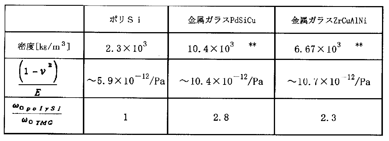
表3から、同じ寸法でダイヤフラムを作製すると、金属ガラス製はポリシリコン製と比べて、圧力センサとしての感度がおおよそ2倍になるものの、共振周波数が1/2から1/3に下がる。圧力センサをマイクロフォンとして用いる場合、設計によっては共振周波数が音声周波数内に入ってきて問題になる可能性がある。したがって、金属ガラスを用いてマイクロフォンのダイヤフラムを作製する際には、材料特性に応じて寸法を最適設計しなくてはならない。式7と式8と式11から分かるように、ダイヤフラムの共振周波数を保ったまま厚さをX倍にすると、それに応じてダイヤフラムの半径aが√X倍に変化し、相対的な感度は1/X倍になる。このことから、ダイヤフラムを薄くしそれに合わせてダイヤフラムを小さくすれば、感度を向上できることがわかる。ただし、ダイヤフラムが薄くなっても十分な耐圧が確保される必要がある。
ここで、Zr53Ti5Cu20Ni12Al10金属ガラス製ダイヤフラムを想定し、材料力学に基づいて具体的な設計を行うと、ポリシリコン製ダイヤフラムに比べて厚さを0.33倍、直径を0.39倍にすれば、おおよそ同じ共振周波数と耐圧が得られる。このとき、相対的な感度はポリシリコン製のそれと比べてほぼ同じ(1.03倍)になる。一方、ダイヤフラムの面積はおおよそ0.15倍になり、感度を保ったままダイの大幅な小型化が可能である。
上述の設計では、ダイヤフラムが大幅に小さくなるので、同一ダイの上に複数のダイヤフラムを搭載することが可能になるが、マトリックス状にM行×N列のダイヤフラムを同一のダイに配置することも可能になり、例えば2行×4列のダイヤフラムを同一ダイの上に配すると、ダイの面積はおおよそ20%しか増えないのに対して、感度は8倍以上に向上する。また、本発明による圧力センサを超音波センサとして用いる場合、複数のダイヤフラムを用いてフェーズドアレイを構成することが可能であり、超音波による物体の距離と方向が測定できる。
さらに、本発明によれば、ダイヤフラムの厚さをダイヤフラム内で変化させ、たとえば、蜂巣状、格子状、放射状、同心円状、あるいはそれらの組み合わせ形状に厚い部分を配置させ、共振周波数と機械的強度を高く保ちつつ感度を向上できる。
図4は、本発明の実施形態に係るマイクロフォン20を構成するダイヤフラム21を示す図であり、上段に平面図を、下段に断面図を示す。マイクロフォン20は、MEMSダイ22を備え、キャビティ23を有する基板24と、基板24上に複数のパーフォレーションホール25を有する対向電極26と、ダイヤフラム21とを備え、少なくともダイヤフラム21と対向電極26とが絶縁されている。基板24には読み出し回路27が搭載されている。ダイヤフラム21は、厚い部分21aが蜂巣状に配置されており、薄い部分21bを区画している。パーフォレーションホール25と厚い部分21aとが対向するようにしてもよいし、厚い部分がダイヤフラム21の反対側に形成されていてもよい。これにより、ダイヤフラム21を金属ガラスで形成しても、確実に強度を持たせることができる。
ダイヤフラムの剛性、またそれと関係する共振周波数はダイヤフラムの応力によっても変化する。したがって、ダイヤフラムの特性を制御するパラメータの一つに応力がある。上記の共振周波数低下の問題を解決する方法の一つに、金属ガラス製のダイヤフラムにおける共振周波数が、Si製のダイヤフラムにおける共振周波数と同程度になるように、ダイヤフラムの応力を引張にする方法がある。ダイヤフラムが引っ張られていることにより共振周波数が高くなるが、0~500MPaの引張応力が好ましい。引張応力とすることでダイヤフラムが破壊しやすくなるという問題があるが、この範囲の引張応力であれば、金属ガラスの優れた機械特性によって解決できる。
図5A乃至図5Gは、本発明の実施形態に係るマイクロフォン30の製造方法を示す図である。図5A乃至図5Gでは、それぞれ上段に平面図を、下段にA-A線に沿った断面図を示している。なお、読み取り回路については図示していない。
Step1として、対向電極となる層(「対向電極層」と呼ぶ。)31cを有する基板31を用意する。基板31には(図示しない)読み取り回路が予め作製されている。具体的には、図5Aに示すように、Si基板31a上にSiO2層31bを有しさらにSiO2層31b上にSi半導体層31cを有するSOI基板31を用意する。
Step2として、対向電極層31cに複数のホール(パーフォレーションホール)32を設ける。具体的には、図5Bに示すように、SOI基板31の表面のSi半導体層31cに複数のホール(パーフォレーションホール)32をエッチングによって設ける。また、Si半導体層31c各隅の部分を矩形状にエッチングし、SiO2層31bを露出させている。このとき、(図示しない)読み取り回路はフォトレジストによって保護する。
Step3として、ホール32を埋めると共に対向電極層31c上に犠牲層33を設ける。具体的には、図5Cに示すように、ホール32を埋めると共にSi半導体層31c上に樹脂(フォトレジスト)の犠牲層33を設ける。必要に応じて、リフローによって樹脂の表面を平坦化する。
Step4として、対向電極層31cの一部及び犠牲層33上に金属ガラスを層状に設ける。具体的には、図5Dに示すように、Si半導体層31cの一部及び犠牲層33上に金属ガラス層34を設ける。ここで、金属ガラスはスパッタ法で成膜し、フォトレジストをマスクにしたエッチングによりパターニングする。図示しない読み取り回路上の金属ガラスも除去する。金属ガラス層34の一部はSiO2層31b上に設けられて支持部34aとなる。ダイヤフラムの厚さを場所によって変える場合には、既設の金属ガラス上にフォトレジストをパターニングし、その上に金属ガラスをスパッタ法で成膜してリフトオフする。
次に、ダイヤフラムと対向電極と読み取り回路とを薄膜配線で接続し(図示せず)、対向電極、犠牲層33、金属ガラス層24を基板31の裏面エッチングによって基板31からリリースする。
具体的には、Step5として、図5Eに示すように、SOI基板31の裏側のSi基板31aの一部をエッチングによって取り除き、キャビティの一部35aを構成する。
Step6として、図5Fに示すように、Si半導体層31cの裏面側まで基板31を取り除き、キャビティ35を形成する。
Step7として、図5Gに示すように、犠牲層33を酸素アッシング、有機溶媒によるエッチング、あるいは原子状水素エッチングによって取り除き、ダイヤフラム36をリリースする。
Step7として、図5Gに示すように、犠牲層33を酸素アッシング、有機溶媒によるエッチング、あるいは原子状水素エッチングによって取り除き、ダイヤフラム36をリリースする。
この一連のプロセスは、高温プロセスを用いておらず低温成膜プロセスであるため、容易にマイクロフォン上に回路を集積化できる。予め作製した読み取り回路とダイヤフラム36との配線、第2のダイとの配線を形成することも容易である。
金属ガラスとしては、前述では、PdSiCuとZrCuAlNiの場合を例にあげたが、Zr系金属ガラス、Pd系金属ガラス、Pt系金属ガラス、Au系金属ガラス、Fe系金属ガラス、Ni系金属ガラス、Mg系金属ガラス、Co系金属ガラス、Cu系金属ガラスの何れかであってもよい。
Zr系金属ガラスとして、Zr53Ti5Cu20Ni12Al10、Zr55Cu30Al10Ni5、Zr75Cu19Al6などがあり、
Pd系金属ガラスとして、Pd40Ni10Cu30P20、Pd78Cu6Si16などがあり、
Pt系金属ガラスとして、Pt58Cu15Ni5P23などがあり、
Au系金属ガラスとして、Au49Ag6Pd2Cu27Si16などがあり、
Fe系金属ガラスとして、Fe76Si9B10P5などがあり、
Ni系金属ガラスとして、Ni60Nb15Ti20Zr5などがあり、
Mg系金属ガラスとして、Mg57Cu34Nd9、Mg64Ni21Nd15などがある。
Co系金属ガラスとして、Co56Ta9B35などがある。
Cu系金属ガラスとして、Cu50Zr50、Cu50Zr45Al5などがある。
これらの金属ガラスはスパッタリング法で膜状に作製することができる。
金属ガラスはZrを主元素とするとよい。これは、引張強度が高く密度が小さく機械特性に優れるだけではなく、Pd、Au、Ptを主成分とする金属ガラスと比べ原材料を安価に入手でき、製造コストを削減するからである。また、磁性がないため磁気ノイズの影響を受けない。Co系の金属ガラスとCu系金属ガラスは密度に対する強度(比強度)が大きく、前者は特に大きい。
以下、実施例によりさらに具体的に説明する。
以下、実施例によりさらに具体的に説明する。
先ず、MEMSマイクロフォン用の新しい材料として、PdCuSiとZrCuAlNiを選択した。金属ガラス膜がスパッタリング法によって堆積できることは従来から知られていたが、MEMS材料としては一般的ではない上、膜応力制御が容易ではなく、0応力から適切な引張応力に膜応力を精密制御しなくてはならないMEMSマイクロフォンに適用するという発想はなく、その可能性も示されていなかった。本発明者らは、基礎検討を行い、スパッタリング法によって成膜した金属ガラスがMEMSマイクロフォンに適用できることを見出した。
PdCuSi金属ガラスを次の条件でスパッタリング法により堆積した。スパッタリングにおいて、高周波電力を100Wとし、Arガス流量を10sccmとし、堆積圧力を1.34Paとし、堆積時間を50分とし、1サイクルを300秒とし、クールダウン時間を300秒とした。基板の回転速度を20rpmとした。PdCuSi金属ガラスの堆積速度は16.6nm/分であった。その後、350℃乃至410℃でアニーリングを行い、膜応力を上記の範囲に調整した。
図6はPdCuSi金属ガラスのAFM像である。この像から、表面粗さRaは0.1nm程度であり、十分平滑な金属ガラス薄膜が形成されていることが分かった。
ZrCuAlNi金属ガラスを次の条件でスパッタリング法により堆積した。スパッタリングにおいて、高周波電力を100Wとし、Arガス流量を15sccmとし、堆積圧力を0.4Paとし、堆積時間を60分とし、1サイクルを300秒とし、クールダウン時間を300秒とした。基板は回転させなかった。ZrCuAlNi金属ガラスの堆積速度は11.83nm/分であった。その後、400℃乃至480℃でアニーリングを行い、膜応力を上記の範囲に調整した。
図7はZrCuAlNi金属ガラスのAFM像である。この像から、表面粗さRaは0.2nm程度であり、十分平滑な金属ガラス薄膜が形成されていることが分かった。
次に、MEMSマイクロフォン構造の試験のために、金属ガラス製ダイヤフラムを次の要領で試作した。図8は、実施例としての金属ガラス製ダイヤフラムの作製方法を示す図である。
Step1として、Si基板61上に犠牲層としてフォトレジト62を堆積し、パターニングした。
Step2として、加熱してフォトレジスト62をリフローした。
Step3として、金属ガラス膜63を堆積し、基板裏面にマスク64をパターニングした。ダイヤフラムの厚さを場所によって変化させる場合、この上にパターニングされた金属ガラス膜をフォトレジストを用いたリフトオフ法によって形成する。
Step4として、基板61のSiをエッチングし、キャビティ65を構成した。
Step5として、酸素アッシング又はアセトンにより犠牲層としてのフォトレジスト62及びマスク64を除去した。
Step2として、加熱してフォトレジスト62をリフローした。
Step3として、金属ガラス膜63を堆積し、基板裏面にマスク64をパターニングした。ダイヤフラムの厚さを場所によって変化させる場合、この上にパターニングされた金属ガラス膜をフォトレジストを用いたリフトオフ法によって形成する。
Step4として、基板61のSiをエッチングし、キャビティ65を構成した。
Step5として、酸素アッシング又はアセトンにより犠牲層としてのフォトレジスト62及びマスク64を除去した。
図9は、実施例としての金属ガラス製ダイヤフラムの別の試作方法を示す図である。
Step1として、Si基板71の両面を酸化してSiO2層72,73とし、一方の面のSiO2層72をパターニングした。
Step2として、SiO2層72を設けた側のホールにフォトレジスト74を設けるようパターニングし、リフローした。
Step3として、スパッタリング法によって金属ガラス膜75を堆積した。
Step4として、バックサイド側のSiO2層73をパターニングした。
Step5として、Si基板71の一部を、KOHによりエッチングし、キャビティ76を形成し、フォトレジスト74を除去した。
Step1として、Si基板71の両面を酸化してSiO2層72,73とし、一方の面のSiO2層72をパターニングした。
Step2として、SiO2層72を設けた側のホールにフォトレジスト74を設けるようパターニングし、リフローした。
Step3として、スパッタリング法によって金属ガラス膜75を堆積した。
Step4として、バックサイド側のSiO2層73をパターニングした。
Step5として、Si基板71の一部を、KOHによりエッチングし、キャビティ76を形成し、フォトレジスト74を除去した。
図10は実施例で作製したダイヤフラムのSEM像である。ダイヤフラムが設計通り作製されていることが分かった。また、空気ノズルで圧力流を加えても破損せず、ダイヤフラムは高い機械的強度を有していることを確認した。
以上、本発明の実施形態及び実施例に関し、圧力センサ及びその例としてマイクロフォンを説明した。なお、信号処理回路を集積回路により構成する場合、信号処理回路での処理について説明する。信号処理回路がアナログ出力である場合、入力回路から入力された信号は、集積回路によってフィルタリング、ゼロ点補正、感度補正、温度補償などをされ、出力バッファ回路を通して電圧が出力される。信号処理回路がデジタル出力である場合、入力回路から入力された信号は、集積回路によってAD変換、フィルタリング、ゼロ点補正、感度補正、温度補償などをされ、最終的にはI2CやSPIといった規格にそってコード化されたデジタル信号として出力される。デジタル回路には、感度や動作モードなどの各種設定を受け付ける機能、さらに自己診断機能を備えていてもよい。
本発明の実施形態はマイクロフォンのみならず空圧センサや超音波センサなどの圧力センサにおいても適用することができる。特に微弱な圧力をダイヤフラムの変位で測定するには、ダイヤフラムが変形し易いことと機械強度を維持することが、ダイヤフラムを金属ガラスで構成したことにより達成される。本発明の実施形態は上述した事項に限定されることなく、例えば次のようにしてもよい。
図示したダイヤフラムは、バックプレート(対向電極)の後ろ側に配置されているが、ダイヤフラムと対向電極の上下の位置関係は逆でも良い。
ダイヤフラムの枠体への固定は一か所でも複数箇所でもよく、ダイヤフラムの周縁部を周状に固定してもよい。
図1、図2などに示すように第1のダイに設けられるダイヤフラムは金属ガラス製である場合のみならず、ポリシリコンなど他の材料で作製されていてもよい。
ダイヤフラムは、一様な厚みであっても、図2に示すように部分的に厚い部位を設けてもよい。さらには、図11に示すように、ダイヤフラム60,70,80にスリット61,71,81を設けて、ダイヤフラムを2分割、3分割、4分割又はそれ以上に分割してもよい。その場合、ダイヤフラムは片持ち式で保持される。また、ダイヤフラムは、平面視で、円形、矩形等の各種形状を有するようにしてもよい。
10:マイクロフォン
11:支持枠
12:ダイヤフラム
13:対向電極
13a:パーフォレーションホール
20:マイクロフォン
21:ダイヤフラム
22:MEMSダイ
23:キャビティ
24:基板
25:パーフォレーションホール
26:対向電極
21a:厚い部分
21b:薄い部分
30:マイクロフォン
31:基板(SOI基板)
31a:基板
31b:SiO2層
31c:対向電極層(半導体層)
32:ホール(パーフォレーションホール)
33:犠牲層
34:金属ガラス層
34a:支持部
35:キャビティ
35a:キャビティの一部
36:ダイヤフラム
60,70,80:ダイヤフラム
61,71,81:スリット
100,200:圧力センサ
101,201:ベース
102,202:第1のダイ
103,203:第2のダイ
104,204:ダイヤフラム
105,205:対向電極
106,206:読み出し回路
106a,206a:入力回路
107,207:信号処理回路(集積回路)
208:バンプ
209:封止材(樹脂)
Claims (6)
- 一つ以上のダイヤフラムと、
前記ダイヤフラムと対向するように設けられた対向電極と、
前記ダイヤフラムの振動信号を受け、前記ダイヤフラムと前記対向電極との静電容量を電圧、電流、周波数の何れかの信号に変換する入力回路と、
前記入力回路からの信号に対しアナログ処理、デジタル処理の何れか又は双方をする信号処理回路と、
を備え、
前記ダイヤフラムと前記入力回路とが第1のダイに設けられ、
前記信号処理回路が第2のダイに設けられ、
前記第1のダイと前記第2のダイとが配線で接続されている、圧力センサ。 - 前記第2のダイに設けられた回路のプロセスルールが、前記第1のダイに設けられた回路のプロセスルールと比較して、小さい、請求項1に記載の圧力センサ。
- 前記信号処理回路は、前記入力回路により変換された信号の入力を受ける、請求項1又は2に記載の圧力センサ。
- 前記入力回路がアンプを含む、請求項1乃至3の何れか1項に記載の圧力センサ。
- 前記ダイヤフラムの数が2個以上16個以下である、請求項1乃至4の何れか1項に記載の圧力センサ。
- 前記第1のダイと前記第2のダイが同一面に並べて配置されている、請求項1乃至5の何れか1項に記載の圧力センサ。
Priority Applications (1)
| Application Number | Priority Date | Filing Date | Title |
|---|---|---|---|
| JP2018508019A JP6650154B2 (ja) | 2016-03-28 | 2017-03-27 | 圧力センサ |
Applications Claiming Priority (2)
| Application Number | Priority Date | Filing Date | Title |
|---|---|---|---|
| JP2016-064779 | 2016-03-28 | ||
| JP2016064779 | 2016-03-28 |
Publications (1)
| Publication Number | Publication Date |
|---|---|
| WO2017170457A1 true WO2017170457A1 (ja) | 2017-10-05 |
Family
ID=59965650
Family Applications (1)
| Application Number | Title | Priority Date | Filing Date |
|---|---|---|---|
| PCT/JP2017/012493 Ceased WO2017170457A1 (ja) | 2016-03-28 | 2017-03-27 | 圧力センサ |
Country Status (2)
| Country | Link |
|---|---|
| JP (1) | JP6650154B2 (ja) |
| WO (1) | WO2017170457A1 (ja) |
Citations (3)
| Publication number | Priority date | Publication date | Assignee | Title |
|---|---|---|---|---|
| JP2003102097A (ja) * | 2001-09-25 | 2003-04-04 | Nippon Hoso Kyokai <Nhk> | 音処理装置 |
| JP2009098022A (ja) * | 2007-10-17 | 2009-05-07 | Rohm Co Ltd | 半導体装置 |
| JP2009124474A (ja) * | 2007-11-15 | 2009-06-04 | Yamaha Corp | 静電型スピーカ |
Family Cites Families (6)
| Publication number | Priority date | Publication date | Assignee | Title |
|---|---|---|---|---|
| JPH06300651A (ja) * | 1993-04-13 | 1994-10-28 | Yazaki Corp | 容量型圧力センサ |
| JP2004147152A (ja) * | 2002-10-25 | 2004-05-20 | Sanyo Electric Co Ltd | 音響センサー及び音響センサーの製造方法 |
| JP4642634B2 (ja) * | 2005-10-31 | 2011-03-02 | パナソニック株式会社 | 音響センサの製造方法 |
| JP2008155333A (ja) * | 2006-12-25 | 2008-07-10 | Japan Science & Technology Agency | 金属ガラスを用いたマイクロマシン及びそれを用いたセンサ並びにその製造方法 |
| TWI336770B (en) * | 2007-11-05 | 2011-02-01 | Ind Tech Res Inst | Sensor |
| US9351084B2 (en) * | 2014-07-14 | 2016-05-24 | Invensense, Inc. | Packaging concept to improve performance of a micro-electro mechanical (MEMS) microphone |
-
2017
- 2017-03-27 JP JP2018508019A patent/JP6650154B2/ja not_active Expired - Fee Related
- 2017-03-27 WO PCT/JP2017/012493 patent/WO2017170457A1/ja not_active Ceased
Patent Citations (3)
| Publication number | Priority date | Publication date | Assignee | Title |
|---|---|---|---|---|
| JP2003102097A (ja) * | 2001-09-25 | 2003-04-04 | Nippon Hoso Kyokai <Nhk> | 音処理装置 |
| JP2009098022A (ja) * | 2007-10-17 | 2009-05-07 | Rohm Co Ltd | 半導体装置 |
| JP2009124474A (ja) * | 2007-11-15 | 2009-06-04 | Yamaha Corp | 静電型スピーカ |
Also Published As
| Publication number | Publication date |
|---|---|
| JP6650154B2 (ja) | 2020-02-19 |
| JPWO2017170457A1 (ja) | 2019-05-30 |
Similar Documents
| Publication | Publication Date | Title |
|---|---|---|
| JP6132047B1 (ja) | 圧力センサとその製造方法 | |
| US9809444B2 (en) | System and method for a differential comb drive MEMS | |
| US10343898B1 (en) | MEMS microphone with tunable sensitivity | |
| EP1996507B1 (en) | Method for fabricating a mems microphone | |
| CN102740200B (zh) | 具有带锥形表面的薄膜支撑的微机械声换能器 | |
| US20210078856A1 (en) | A mems microphone, a manufacturing method thereof and an electronic apparatus | |
| WO2010079574A1 (ja) | Memsデバイス | |
| US20160330550A1 (en) | Integrated package forming wide sense gap micro electro-mechanical system microphone and methodologies for fabricating the same | |
| CN108924720A (zh) | Mems麦克风 | |
| US11524891B2 (en) | Membrane support for dual backplate transducers | |
| US9668064B2 (en) | Microelectromechanical system microphone | |
| Wang et al. | Micropatterned PDMS damping layer integration to enhance the fidelity of piezoelectric MEMS speakers without SPL penalty | |
| US20240137711A1 (en) | Capacitive microphone sensor design and fabrication method for achieving higher signal to noise ratio | |
| WO2014045042A1 (en) | Mems device and process | |
| TW200914364A (en) | MEMS device and process | |
| JP6650154B2 (ja) | 圧力センサ | |
| US7239712B1 (en) | Inductor-based MEMS microphone | |
| KR101787878B1 (ko) | 압저항형 가속도계 | |
| US20250159423A1 (en) | Foundry-compatible process for a mems audio device | |
| TWI498272B (zh) | Microelectromechanical system device and manufacturing method thereof | |
| Huang et al. | Design and implementation of a novel CMOS MEMS condenser microphone with corrugated diaphragm | |
| JP2007104466A (ja) | 音響センサおよびその製造方法 |
Legal Events
| Date | Code | Title | Description |
|---|---|---|---|
| NENP | Non-entry into the national phase |
Ref country code: DE |
|
| 121 | Ep: the epo has been informed by wipo that ep was designated in this application |
Ref document number: 17774994 Country of ref document: EP Kind code of ref document: A1 |
|
| ENP | Entry into the national phase |
Ref document number: 2018508019 Country of ref document: JP Kind code of ref document: A |
|
| 122 | Ep: pct application non-entry in european phase |
Ref document number: 17774994 Country of ref document: EP Kind code of ref document: A1 |