WO2017168649A1 - 熱硬化性樹脂組成物、光半導体素子搭載用基板及びその製造方法並びに光半導体装置 - Google Patents
熱硬化性樹脂組成物、光半導体素子搭載用基板及びその製造方法並びに光半導体装置 Download PDFInfo
- Publication number
- WO2017168649A1 WO2017168649A1 PCT/JP2016/060472 JP2016060472W WO2017168649A1 WO 2017168649 A1 WO2017168649 A1 WO 2017168649A1 JP 2016060472 W JP2016060472 W JP 2016060472W WO 2017168649 A1 WO2017168649 A1 WO 2017168649A1
- Authority
- WO
- WIPO (PCT)
- Prior art keywords
- resin composition
- optical semiconductor
- thermosetting resin
- semiconductor element
- silicone resin
- Prior art date
- Legal status (The legal status is an assumption and is not a legal conclusion. Google has not performed a legal analysis and makes no representation as to the accuracy of the status listed.)
- Ceased
Links
Images



Classifications
-
- C—CHEMISTRY; METALLURGY
- C08—ORGANIC MACROMOLECULAR COMPOUNDS; THEIR PREPARATION OR CHEMICAL WORKING-UP; COMPOSITIONS BASED THEREON
- C08L—COMPOSITIONS OF MACROMOLECULAR COMPOUNDS
- C08L83/00—Compositions of macromolecular compounds obtained by reactions forming in the main chain of the macromolecule a linkage containing silicon with or without sulfur, nitrogen, oxygen or carbon only; Compositions of derivatives of such polymers
- C08L83/04—Polysiloxanes
-
- C—CHEMISTRY; METALLURGY
- C08—ORGANIC MACROMOLECULAR COMPOUNDS; THEIR PREPARATION OR CHEMICAL WORKING-UP; COMPOSITIONS BASED THEREON
- C08K—Use of inorganic or non-macromolecular organic substances as compounding ingredients
- C08K3/00—Use of inorganic substances as compounding ingredients
- C08K3/18—Oxygen-containing compounds, e.g. metal carbonyls
- C08K3/20—Oxides; Hydroxides
- C08K3/22—Oxides; Hydroxides of metals
-
- C—CHEMISTRY; METALLURGY
- C08—ORGANIC MACROMOLECULAR COMPOUNDS; THEIR PREPARATION OR CHEMICAL WORKING-UP; COMPOSITIONS BASED THEREON
- C08K—Use of inorganic or non-macromolecular organic substances as compounding ingredients
- C08K3/00—Use of inorganic substances as compounding ingredients
- C08K3/18—Oxygen-containing compounds, e.g. metal carbonyls
- C08K3/20—Oxides; Hydroxides
- C08K3/22—Oxides; Hydroxides of metals
- C08K3/2279—Oxides; Hydroxides of metals of antimony
-
- C—CHEMISTRY; METALLURGY
- C08—ORGANIC MACROMOLECULAR COMPOUNDS; THEIR PREPARATION OR CHEMICAL WORKING-UP; COMPOSITIONS BASED THEREON
- C08K—Use of inorganic or non-macromolecular organic substances as compounding ingredients
- C08K7/00—Use of ingredients characterised by shape
- C08K7/22—Expanded, porous or hollow particles
-
- H—ELECTRICITY
- H10—SEMICONDUCTOR DEVICES; ELECTRIC SOLID-STATE DEVICES NOT OTHERWISE PROVIDED FOR
- H10H—INORGANIC LIGHT-EMITTING SEMICONDUCTOR DEVICES HAVING POTENTIAL BARRIERS
- H10H20/00—Individual inorganic light-emitting semiconductor devices having potential barriers, e.g. light-emitting diodes [LED]
- H10H20/80—Constructional details
- H10H20/85—Packages
-
- H—ELECTRICITY
- H10—SEMICONDUCTOR DEVICES; ELECTRIC SOLID-STATE DEVICES NOT OTHERWISE PROVIDED FOR
- H10W—GENERIC PACKAGES, INTERCONNECTIONS, CONNECTORS OR OTHER CONSTRUCTIONAL DETAILS OF DEVICES COVERED BY CLASS H10
- H10W72/00—Interconnections or connectors in packages
- H10W72/851—Dispositions of multiple connectors or interconnections
- H10W72/874—On different surfaces
- H10W72/884—Die-attach connectors and bond wires
-
- H—ELECTRICITY
- H10—SEMICONDUCTOR DEVICES; ELECTRIC SOLID-STATE DEVICES NOT OTHERWISE PROVIDED FOR
- H10W—GENERIC PACKAGES, INTERCONNECTIONS, CONNECTORS OR OTHER CONSTRUCTIONAL DETAILS OF DEVICES COVERED BY CLASS H10
- H10W74/00—Encapsulations, e.g. protective coatings
-
- H—ELECTRICITY
- H10—SEMICONDUCTOR DEVICES; ELECTRIC SOLID-STATE DEVICES NOT OTHERWISE PROVIDED FOR
- H10W—GENERIC PACKAGES, INTERCONNECTIONS, CONNECTORS OR OTHER CONSTRUCTIONAL DETAILS OF DEVICES COVERED BY CLASS H10
- H10W90/00—Package configurations
- H10W90/701—Package configurations characterised by the relative positions of pads or connectors relative to package parts
- H10W90/721—Package configurations characterised by the relative positions of pads or connectors relative to package parts of bump connectors
- H10W90/726—Package configurations characterised by the relative positions of pads or connectors relative to package parts of bump connectors between a chip and a stacked lead frame, conducting package substrate or heat sink
Definitions
- the present invention relates to a thermosetting resin composition, a substrate for mounting an optical semiconductor element using the thermosetting resin composition, a method for manufacturing the same, and an optical semiconductor device.
- Thermosetting resins are used in a wide range of applications because they exhibit various excellent properties derived from their unique cross-linked structure.
- an optical semiconductor device in which an optical semiconductor element such as an LED (Light Emitting Diode) and a phosphor is combined is used for an outdoor display or a portable device because of advantages such as high energy efficiency and long life. It is applied to various applications such as liquid crystal backlights and in-vehicle applications, and its demand is expanding.
- One type of optical semiconductor device is a surface-mounted optical semiconductor device.
- Some surface-mount optical semiconductor devices have an optical semiconductor element and a reflector (reflecting portion) provided so as to surround the optical semiconductor element.
- Patent Document 1 discloses a resin composition for a mounting package for housing an optical semiconductor element using a silicone resin having a structure in which any one of a vinyl group and an allyl group and a hydrogen atom is directly bonded to a silicon atom. Has been.
- Patent Literature 2 describes a resin sealing device for sealing and molding an electronic component mounted on a lead frame at the time of transfer molding with a resin material. A method for sealing is disclosed.
- the present invention has been made in view of the above circumstances, and is a thermosetting resin composition capable of forming a tough molded body in which cracks and cracks are unlikely to occur, and light using the thermosetting resin composition It is an object of the present invention to provide a semiconductor element mounting substrate, a method for manufacturing the same, and an optical semiconductor device.
- the present invention relates to a thermosetting resin composition containing a silicone resin and a pigment containing a hydrosilyl group-containing silicone resin and an alkenyl group-containing silicone resin having an alkenyl group equivalent of 50 to 1000 g / mol.
- the alkenyl group-containing silicone resin may have 75 mol% or more of alkenyl groups based on the total amount of organic groups bonded to silicon atoms.
- the alkenyl group-containing silicone resin may have a weight average molecular weight of 200 to 10,000.
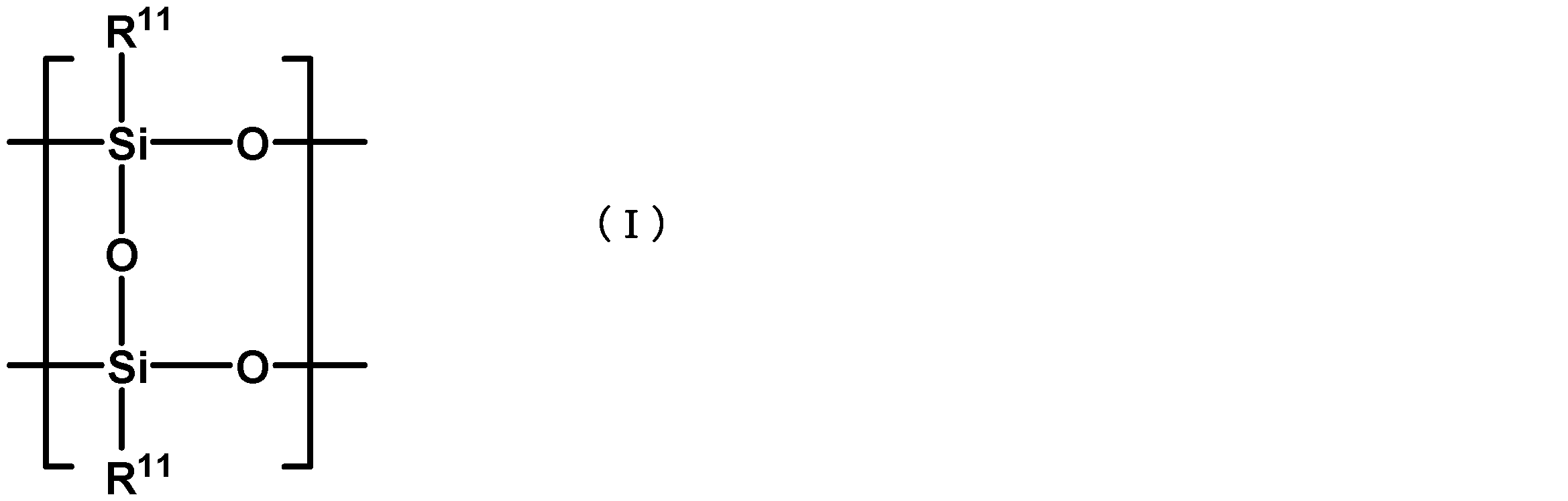
- alkenyl group-containing silicone resin may have a structure represented by the following formula (I). [Wherein, each R 11 independently represents an alkenyl group. ]
- thermosetting resin composition of the present invention may contain 0.0005 to 35% by mass of the alkenyl group-containing silicone resin based on the total amount of the thermosetting resin composition.
- the pigment is at least one selected from the group consisting of titanium oxide, zinc oxide, alumina, magnesium oxide, antimony oxide, and zirconium oxide.
- the white pigment may be included, and hollow particles may be included.
- the present invention also relates to a cured product formed from the thermosetting resin composition.
- the present invention relates to an optical semiconductor element mounting substrate having a molded body formed from the thermosetting resin composition described above.
- the optical semiconductor element mounting substrate has a recess composed of a bottom surface and a wall surface, the bottom surface of the recess is a mounting portion for the optical semiconductor element, and at least a part of the wall surface of the recess is the thermosetting resin composition described above. It is the molded object formed from the thing.
- the optical semiconductor element mounting substrate of the present invention includes a substrate, a first connection terminal and a second connection terminal provided on the substrate, and the first connection terminal and the second connection terminal are provided. In between, you may have the molded object formed from the above-mentioned thermosetting resin composition.
- the present invention relates to an optical semiconductor device comprising the optical semiconductor element mounting substrate and an optical semiconductor element mounted on the optical semiconductor element mounting substrate.
- the present invention also relates to a method for manufacturing a substrate for mounting an optical semiconductor element having a recess composed of a bottom surface and a wall surface.
- the manufacturing method according to the present invention includes a step of forming at least a part of the wall surface of the recess by transfer molding or compression molding using the thermosetting resin composition described above.
- thermosetting resin composition capable of forming a tough cured product that is less likely to crack and crack, a substrate for mounting an optical semiconductor element using the thermosetting resin composition, and a method for manufacturing the same.
- an optical semiconductor device can be provided.
- thermosetting resin composition contains a silicone resin and a pigment containing a hydrosilyl group-containing silicone resin and an alkenyl group-containing silicone resin having an alkenyl group equivalent of 50 to 1000 g / mol.
- a silicone resin and a pigment containing a hydrosilyl group-containing silicone resin and an alkenyl group-containing silicone resin having an alkenyl group equivalent of 50 to 1000 g / mol contains a silicone resin and a pigment containing a hydrosilyl group-containing silicone resin and an alkenyl group-containing silicone resin having an alkenyl group equivalent of 50 to 1000 g / mol.
- each component contained in the thermosetting resin composition of this embodiment is demonstrated.
- the hydrosilyl group-containing silicone resin is not particularly limited as long as it is a silicone resin having a hydrosilyl group that is a group (Si—H) in which a hydrogen atom is directly bonded to a silicon atom.
- the hydrosilyl group-containing silicone resin may have, for example, a unit represented by HSiO 3/2 , a unit represented by HSiO 2/2 , or a unit represented by HSiO 1/2 as a structural unit having a hydrosilyl group. it can.
- the structural unit having a hydrosilyl group is, for example, methylmethoxydisilane, dimethoxydisilane, methoxytrisilane, ethylmethoxydisilane, dimethylethoxysilane, propyldiethoxysilane, propylethoxydisilane, n-butyldimethoxysilane, phenyldimethoxysilane, phenylmethoxy Alkoxyhydroxysilanes such as disilane and triethoxysilane; methyldichlorosilane, n-propyldichlorosilane, isopropyldichlorosilane (1,1-dichloro-2-methyl-1-silapropane), n-butyldichlorosilane, n-pentyldi It can introduce
- the hydrosilyl group-containing silicone resin may have a structure in which a group other than a hydrogen atom is bonded to a silicon atom, that is, a structural unit other than a hydrosilyl group.
- the structural unit other than the hydrosilyl group include a structural unit in which an organic group having 1 to 12 carbon atoms is bonded to a silicon atom. From the viewpoint of ease of synthesis, an organic group having 1 to 8 carbon atoms is silicon. It may be a structural unit bonded to an atom.
- the organic group is preferably a hydrocarbon group from the viewpoint of ease of synthesis, and examples of the hydrocarbon group include an alkyl group, a cycloalkyl group, an aralkyl group, and an aryl group.
- Examples of the alkyl group include a methyl group, an ethyl group, and a propyl group.
- Examples of the cycloalkyl group include a cyclopentyl group and a cyclohexyl group.
- Examples of the aralkyl group include a benzyl group.
- Examples of the aryl group include a phenyl group, a tolyl group, and a xylyl group. These groups may be halogenated hydrocarbon groups in which hydrogen atoms are partially substituted with chlorine atoms, fluorine atoms, or the like. From the viewpoint of further improving the ease of synthesis and hardness of the silicone resin, the organic group is preferably an aryl group, and more preferably a phenyl group.
- the hydrosilyl group-containing silicone resin may have a unit represented by R 1 SiO 3/2 as a structural unit other than the hydrosilyl group, and a unit represented by R 1 SiO 3/2 and R 2 SiO It may have at least one unit selected from a unit represented by 2/2 , a unit represented by R 3 SiO 1/2 and a unit represented by SiO 4/2 .
- R 1 , R 2 and R 3 each independently represent a monovalent organic group, and are preferably a hydrocarbon group having 1 to 12 carbon atoms from the viewpoint of availability.
- a hydrocarbon group the same thing as the hydrocarbon group mentioned above is illustrated.
- R 1 , R 2 and R 3 are preferably each independently an alkyl group or an aryl group, and more preferably a methyl group or a phenyl group.
- the weight average molecular weight of the hydrosilyl group-containing silicone resin is not particularly limited, but from the viewpoint of improving the moldability of the thermosetting resin composition, it is preferably 200 or more, more preferably 1000 or more, and 2000 or more. Further preferred.
- the weight average molecular weight of the hydrosilyl group-containing silicone resin is preferably 15000 or less, more preferably 10,000 or less, and further preferably 7000 or less, from the viewpoint of further improving the hardness of the cured product. That is, the weight average molecular weight of the hydrosilyl group-containing silicone resin may be 200 to 15000, 1000 to 10,000, or 2000 to 7000.
- the weight average molecular weight Mw in the present specification can be obtained by measuring under the following conditions using a standard polystyrene calibration curve by gel permeation chromatography (GPC).
- GPC conditions Pump: L-6200 type (manufactured by Hitachi, Ltd., trade name) Column: TSKgel-G5000HXL and TSKgel-G2000HXL (trade name, manufactured by Tosoh Corporation) Detector: L-3300RI type (manufactured by Hitachi, Ltd., trade name)
- Eluent Tetrahydrofuran Measurement temperature: 30 ° C Flow rate: 1.0 mL / min
- the content of the hydrosilyl group-containing silicone resin in the thermosetting resin composition is not particularly limited, but from the viewpoint of improving the moldability of the thermosetting resin composition, 0.01 to 40 mass with respect to the entire resin composition. %, More preferably 0.1 to 35% by mass, and still more preferably 1.0 to 30% by mass.
- the thermosetting resin composition of the present embodiment contains an alkenyl group-containing silicone resin having an alkenyl group equivalent of 50 to 1000 g / mol.
- the alkenyl group equivalent represents the weight of the alkenyl group-containing silicone resin necessary to obtain 1 mol of alkenyl group.
- the alkenyl group can form a cured product of the thermosetting resin composition by an addition reaction with the hydrosilyl group contained in the above-described hydrosilyl group-containing silicone resin, preferably in the presence of a curing catalyst.
- the alkenyl group equivalent is within the above range, the resin structure after curing has a high crosslink density.
- a cause of cracks or cracks in the molded body is that the molded body has low hardness. That is, since it is difficult to control the transport of the molded body by a machine, the molded body cannot withstand the impact generated during transport.
- the molded body is a reflector of an optical semiconductor device, since it has a complicated shape, pressure tends to concentrate on a part thereof, and the possibility that a crack or a crack will occur increases.
- the above alkenyl group-containing silicone resin since the above alkenyl group-containing silicone resin is used, the number of portions capable of hydrosilylation reaction increases, and the formed cured product has a high crosslinking density. Therefore, it becomes possible to obtain a molded body having high hardness.
- a molded body having high hardness can reduce the occurrence of cracks or cracks and improve the productivity of the optical semiconductor device.
- the alkenyl group equivalent of the alkenyl group-containing silicone resin is preferably 50 to 500 g / mol, more preferably 50 to 300 g / mol, and more preferably 50 to More preferably, it is 250 g / mol.
- X represents an iodine value
- Y represents an alkenyl group equivalent
- M I2 represents a molecular weight of an iodine molecule.
- the iodine value can be calculated by adding iodine to an unsaturated bond and titrating excess iodine with a sodium thiosulfate solution according to the method described in JIS K 0070: 1992.
- the alkenyl group present in the silicone resin is not necessarily bonded directly to the silicon atom.
- Examples of the alkenyl group include vinyl group, allyl group, 1-butenyl group, 2-butenyl group and 2-pentenyl group.
- the alkenyl group is preferably a vinyl group from the viewpoint of heat resistance and light resistance.
- the alkenyl group can be introduced into the silicone resin using, for example, a silane compound having an alkenyl group.
- silane compound having an alkenyl group examples include vinyltrimethoxysilane, vinyltriethoxysilane, vinyltris (2-methoxyethoxy) silane, methylvinyldimethoxysilane, allyltrimethoxysilane, allyltriethoxysilane, and methylallyldimethoxysilane.
- alkenylalkoxysilane alkenylalkoxysilane.
- the alkenyl group-containing silicone resin preferably has a ladder structure as a siloxane skeleton.
- the ladder structure refers to a structure in which adjacent structural units are connected via two or more atoms.
- silicone resin having a ladder structure examples include compounds having a structural unit as shown in the following formula (I).
- each R 11 independently represents an alkenyl group.
- the following formula (I) has the above structural unit and two oxygen atoms that connect the structural unit, and the silicone resin having a ladder structure is represented by (R 11 SiO 3/2 ) 2. It may have a structure.
- the silicone resin having a ladder structure preferably has a structure represented by the formula (I) continuously.
- the silicone resin can have a structure represented by the following formula (I ′), for example.
- formula (I ′) three sets of structural units, two sets of two oxygen atoms connecting them, and two oxygen atoms connecting constituent units (not shown) adjacent to the right are 1 It is understood that you have a pair.
- the number of repeating units of the structure represented by the formula (I) is not particularly limited, but from the viewpoint of further improving the crosslinking density after curing, it is 3 to 5000. It is preferably 5 to 3000, more preferably 10 to 2000.
- the alkenyl group-containing silicone resin may have a group other than the alkenyl group.
- the structural unit having a group other than an alkenyl group include a structural unit represented by R 4 SiO 3/2 or R 5 SiO 2/2 . That is, the alkenyl group-containing silicone resin has a structure represented by the formula (I) ((R 11 SiO 3/2 ) 2 ) and a structure represented by R 4 SiO 3/2 or R 5 SiO 2/2. You may do it.
- R 4 and R 5 each independently represent a monovalent organic group, and are preferably a hydrocarbon group having 1 to 12 carbon atoms from the viewpoint of availability. As a hydrocarbon group, the same thing as above-mentioned R ⁇ 1 >, R ⁇ 2 > and R ⁇ 3 > is illustrated.
- the alkenyl group-containing silicone resin preferably has 75% by mole or more of alkenyl groups, more preferably 85% by mole or more, and more preferably 95% by mole or more based on the total amount of organic groups directly bonded to silicon. preferable.
- the crosslink density of the cured resin is further increased, the cured product of the thermosetting resin composition is hard and difficult to break, and is further improved by automatic transportability during continuous molding. It will be excellent.
- the upper limit of the amount of alkenyl groups present in the alkenyl group-containing silicone resin is preferably as large as possible, and may be 100 mol%.
- the amount of alkenyl group can be calculated by measuring 1 H-NMR of the silicone resin.
- the alkenyl group-containing silicone resin preferably has at least 22 mol%, more preferably at least 23 mol%, and even more preferably at least 24 mol%, based on the total amount of elements directly bonded to silicon. .
- the cured product of the thermosetting resin composition is hard and difficult to break, and is more excellent in automatic transportability during continuous molding.
- the upper limit of the amount of alkenyl groups present in the alkenyl group-containing silicone resin is not particularly limited, but may be 30 mol%.
- the amount of alkenyl group can be calculated by measuring 1 H-NMR of the silicone resin.
- the weight average molecular weight of the alkenyl group-containing silicone resin is not particularly limited, but is preferably 200 or more, more preferably 800 or more, and 1200 or more from the viewpoint of improving the moldability of the thermosetting resin composition. Further preferred. From the viewpoint of further improving the hardness of the cured product, the weight average molecular weight of the alkenyl group-containing silicone resin is preferably 10,000 or less, more preferably 8000 or less, and even more preferably 7000 or less. That is, the weight average molecular weight of the alkenyl group-containing silicone resin may be 200 to 10,000, 800 to 8000, or 1200 to 7000.
- the content of the alkenyl group-containing silicone resin according to this embodiment in the thermosetting resin composition is not particularly limited.
- the alkenyl group-containing silicone resin according to this embodiment is, for example, preferably 0.001 to 70 parts by mass, more preferably 0.01 to 65 parts by mass with respect to 100 parts by mass of the total amount of the silicone resin. More preferably, it is 0.1 to 60 parts by mass.
- the alkenyl group-containing silicone resin according to this embodiment is preferably 0.0005 to 35% by mass, more preferably 0.008 to 30% by mass, based on the total amount of the resin composition. More preferably, the content is 01 to 20% by mass. Within this range, the thermosetting resin composition is more excellent in moldability.
- the alkenyl group-containing silicone resin may be used after diluted in an organic solvent in order to further improve the handleability.
- organic solvent include, but are not limited to, alcohol solvents such as ethanol, propanol, butanol, methyl cellosolve, butyl cellosolve, and propylene glycol monomethyl ether; ketone solvents such as acetone, methyl ethyl ketone, methyl isobutyl ketone, and cyclohexanone; tetrahydrofuran Ether solvents such as toluene; aromatic solvents such as toluene, xylene and mesitylene.
- the organic solvent may be an alcohol solvent, a ketone solvent, or a nitrogen atom-containing solvent.
- the mixing ratio of the alkenyl group-containing silicone resin and the hydrosilyl group-containing silicone resin in the silicone resin is not particularly limited, but from the viewpoint of further enhancing the strength and heat resistance, the number of SiH groups (Y) in the hydrosilyl group-containing silicone resin
- the ratio (Y / X, molar ratio) to the number (X) of alkenyl groups in the alkenyl group-containing silicone resin component is preferably 0.3 ⁇ Y / X ⁇ 3, and 0.5 ⁇ Y / X More preferably, ⁇ 2, more preferably 0.7 ⁇ Y / X ⁇ 1.5.
- the silicone resin according to this embodiment can contain other silicone resins in addition to the above-described hydrosilyl group-containing silicone resin and alkenyl group-containing silicone resin as long as the effects of the present invention are not impaired.
- the resin composition of the present embodiment preferably contains a curing catalyst that promotes the hydrosilylation reaction of the silicone resin.
- the curing catalyst include a calsted catalyst; platinum alone; a carrier (alumina, silica, carbon black, etc.) supported with solid platinum; chloroplatinic acid; a complex of chloroplatinic acid and alcohol, aldehyde, ketone, etc. Platinum-olefin complexes; platinum-vinylsiloxane complexes; platinum-phosphine complexes; platinum-phosphite complexes and dicarbonyldichloroplatinum. These curing catalysts may be used alone or in combination of two or more.
- platinum-olefin complex examples include Pt (CH 2 ⁇ CH 2 ) 2 (PPh 3 ) 2 and Pt (CH 2 ⁇ CH 2 ) 2 Cl 2 .
- platinum-vinylsiloxane complex examples include platinum-2,4,6,8-tetramethyl-2,4,6,8-tetravinylcyclotetrasiloxane complex and platinum-1,3-divinyltetramethyldisiloxane complex. Is mentioned.
- platinum-phosphine complex examples include platinum- (PPh 3 ) 4 and platinum- (PBu 3 ) 4 .
- platinum-phosphite complex examples include platinum- [P (OPh) 3 ] 4 and platinum- [P (OBu) 3 ] 4 .
- Bu represents a butyl group
- Ph represents a phenyl group.
- chloroplatinic acid platinum-olefin complexes or platinum-vinylsiloxane complexes are preferable from the viewpoint of catalytic activity.
- the amount of the curing catalyst contained in the thermosetting resin composition is not particularly limited, but from the viewpoint of further improving the curability of the thermosetting resin composition, 0.005 with respect to 100 parts by mass of the total amount of the silicone resin. Is preferably 0.5 to 0.5 parts by mass, more preferably 0.01 to 0.3 parts by mass, and still more preferably 0.01 to 0.2 parts by mass.
- the amount of the curing catalyst relative to the entire resin composition is preferably 0.01 to 3 ppm, more preferably 0.05 to 2.5 ppm in terms of metal weight, from the viewpoint of further improving curability. More preferably, the content is 0.08 to 2.2 ppm.
- a pigment adds the color according to a use to the hardened
- the pigment which concerns on this embodiment can be selected according to the intended purpose of the hardened
- the pigment include a white pigment, a black pigment, a red pigment, a yellow pigment, an orange pigment, a purple (dark blue) pigment, a blue pigment, and a green pigment.
- the pigment may be an azo pigment, a lake pigment or a fluorescent pigment.
- Examples of the black pigment include carbon black.
- Examples of red pigments include red lead, iron oxide red, quinacridone, diketopyrrolopyrrole, anthraquinone, perylene, perinone, and indigoid.
- Examples of yellow pigments include chrome lead and zinc yellow.
- Examples of blue pigments include ultramarine blue, prussian blue (potassium ferrocyanide), phthalocyanine blue, anthraquinone, and indigoid.
- Examples of the orange pigment include diketopyrrolopyrrole, perylene, anthraquinone, perinone, quinacridone, and indigoid.
- purple (dark blue) color pigments examples include dioxazine, quinacridone, perylene, indigoid, anthraquinone, and xanthene.
- green pigment examples include phthalocyanine, azomethine, and perylene. These pigments may be used alone or in combination of two or more.
- thermosetting resin composition When a light reflection property is required for the thermosetting resin composition, it is preferable to use a white pigment as the pigment.
- the thermosetting resin composition contains a white pigment, the cured product of the thermosetting resin composition has an excellent reflectance, and when used as a light reflecting material provided in a substrate for mounting an optical semiconductor element In addition, a high-brightness optical semiconductor device can be obtained.
- white pigments include titanium oxide, zinc oxide, alumina, magnesium oxide, antimony oxide, zirconium oxide, and the like, and titanium oxide, alumina, and zinc oxide are preferable from the viewpoint of obtaining better light reflectivity. These may be used alone or in combination of two or more.
- hollow particles may be used.
- the hollow particle is a particle having a void inside, and the substance constituting the outer shell is not particularly limited. Hollow particles are useful as white pigments because they refract and reflect incident light at the surface and inner wall.
- the hollow particles include inorganic hollow particles and organic hollow particles.
- metal oxides such as inorganic glass and silica; metal salts such as calcium carbonate, barium carbonate, calcium silicate, and nickel carbonate can be preferably used.
- sodium silicate glass Aluminum silicate glass, borosilicate soda glass, shirasu particles and the like.
- the organic hollow particles polystyrene resins, poly (meth) acrylate resins, and cross-linked products thereof can be suitably used.
- the outer shell of the hollow particles is at least one selected from the group consisting of sodium silicate glass, aluminum silicate glass, borosilicate soda glass, shirasu, crosslinked styrene resin, and crosslinked acrylic resin. It is preferable that it is comprised from the material of these.
- the particle size of the white pigment is not particularly limited, but is preferably in the range of 0.05 to 50 ⁇ m, more preferably in the range of 0.08 to 30 ⁇ m, and 0.1 to 10 ⁇ m. More preferably, it is in the range.
- the center particle diameter of the white pigment is 0.1 ⁇ m or more, the dispersibility becomes better, and when it is 50 ⁇ m or less, the light reflection property of the cured product becomes better.
- the central particle diameter can be determined as a mass average value D 50 (or median diameter) in particle size distribution measurement by a laser light diffraction method.
- the pigment content in the thermosetting resin composition is preferably in the range of 1 to 90% by mass, more preferably in the range of 5 to 90% by mass, based on the total amount of the resin composition. More preferably, it is mass%.
- the white pigment is used, if the content is 1% by mass or more, the light reflection property of the cured product is further improved, and if it is 90% by mass or less, the moldability of the thermosetting resin composition is further improved.
- the pigment content is preferably 50 to 2000 parts by mass, more preferably 80 to 1700 parts by mass, and more preferably 100 to 1500 parts by mass with respect to 100 parts by mass of the total amount of the silicone resin. More preferably, it is part.
- thermosetting resin composition includes inorganic fillers, coupling agents, curing retarders, thermosetting resins other than silicone resins, antioxidants, mold release agents, dispersants, ion scavengers, and the like. These various additives can be further contained.
- the thermosetting resin composition preferably contains an inorganic filler.
- the inorganic filler include silica, antimony oxide, aluminum hydroxide, magnesium hydroxide, barium sulfate, magnesium carbonate, and barium carbonate.
- thermosetting resin composition contains two or more kinds of substances having the effects of both the pigment and the inorganic filler, one of the substances belongs to the inorganic filler.
- substances other than titanium oxide, zinc oxide, alumina, magnesium oxide, antimony oxide and zirconium oxide are given priority as substances belonging to the inorganic filler.
- the center particle size of the inorganic filler is preferably in the range of 0.1 to 100 ⁇ m, more preferably in the range of 0.4 to 80 ⁇ m, from the viewpoint of improving the packing efficiency with the pigment. More preferably, it is 5 to 75 ⁇ m.
- the content of the inorganic filler in the thermosetting resin composition is in the range of 4 to 85% by mass on the basis of the total amount of components that become a solid content after the thermosetting resin composition is cured from the viewpoint of further improving moldability. It is preferably 10 to 80% by mass, more preferably 20 to 80% by mass.
- the total amount of the inorganic filler and the pigment contained in the thermosetting resin composition is preferably 6 to 98% by mass based on the total amount of the resin composition,
- the content is more preferably 15 to 95% by mass, and further preferably 30 to 90% by mass.
- a coupling agent may be added to the thermosetting resin composition as necessary.
- a coupling agent By including a coupling agent, the interfacial adhesion between the silicone resin and inorganic components such as pigments and inorganic fillers can be improved.
- the coupling agent include silane coupling agents and titanate coupling agents.
- silane coupling agent generally known compounds such as epoxy silane, amino silane, cationic silane, vinyl silane, acrylic silane, and mercapto silane can be used.
- the coupling agent may be a composite system of the silane coupling agent. From the viewpoint of improving curability, the amount of the coupling agent used is preferably 0.01 to 5% by mass based on the total amount of the thermosetting resin composition.
- a pigment or an inorganic filler may be previously treated with the above coupling agent.
- a curing retarder may be added to the thermosetting resin composition from the viewpoints of improving storage stability and adjusting reactivity.
- the curing retarder include a compound containing an aliphatic unsaturated bond, an organic phosphorus compound, an organic sulfur compound, a nitrogen-containing compound, a tin-based compound, and an organic peroxide.
- Examples of the compound containing an aliphatic unsaturated bond include propargyl alcohols, ene-yne compounds, maleate esters and the like.
- Examples of the organophosphorus compound include triorganophosphine, diorganophosphine, organophosphon, and triorganophosphite.
- Examples of the organic sulfur compound include organomercaptans, diorganosulfides, hydrogen sulfide, benzothiazole, benzothiazole disulfide and the like.
- Examples of nitrogen-containing compounds include ammonia, primary to tertiary alkylamines, arylamines, urea, hydrazine and the like.
- tin compounds include stannous halide dihydrate and stannous carboxylate.
- organic peroxide include di-t-butyl peroxide, dicumyl peroxide, benzoyl peroxide, and t-butyl perbenzoate.
- a hardening retarder may be used independently or may use 2 or more types together.
- the addition amount of the curing retarder is preferably in the range of 0.1 to 100 mol, more preferably in the range of 1 to 50 mol, with respect to 1 mol of the curing catalyst used.
- thermosetting resin composition it is possible to add a thermosetting resin other than the silicone resin within a range that does not adversely affect the characteristics for the purpose of modifying the characteristics.
- thermosetting resin include, but are not limited to, an epoxy resin, an acrylic resin, a cyanate resin, a phenol resin, a polyimide resin, a polyamideimide resin, and a urethane resin.
- an epoxy resin is preferable from the viewpoint of excellent adhesion to metal parts.
- thermosetting resin those which are colorless or relatively uncolored such as pale yellow are preferable.
- the epoxy resin is not particularly limited.
- hexafluorobisphenol A type diglycidyl ether hydrogenated bisphenol A type diglycidyl ether, bisphenol A diglycidyl ether, 2,2′-bis (4-glycidyloxycyclohexyl) propane.
- the curing agent is preferably an acid anhydride curing agent.
- the acid anhydride curing agent include hexahydrophthalic anhydride, methylhexahydrophthalic anhydride, tetrahydrophthalic anhydride, and methyl hydride.
- examples thereof include nadic acid anhydride, trimellitic acid anhydride, pyromellitic acid anhydride, and anhydrides of aliphatic acids (cyclohexanedicarboxylic acid, cyclohexanetricarboxylic acid, etc.).
- These epoxy resins or curing agents may be used alone or in combination of two or more.
- the light reflectance after curing is preferably 80% or more at any wavelength of 440 to 700 nm. If the light reflectance is 80% or more, the luminance of the optical semiconductor device can be further improved. Further, from the viewpoint of being suitable for an optical semiconductor device using a blue light emitting diode, the light reflectivity at a wavelength of 460 nm after curing is preferably 80% or more, and more preferably 90% or more.
- the light reflectance of the cured product is a wavelength of 440 to 700 nm after a heat resistance test in which the cured product is exposed to an environment of 150 ° C. for 1000 hours. In any of the cases, it is preferably 80% or more. Further, from the viewpoint of being suitable for an optical semiconductor device using a blue light emitting diode, the light reflectance at a wavelength of 460 nm is more preferably 85% or more and 90% or more at the time of measurement after the heat resistance test described above. More preferably.
- thermosetting resin composition can be realized by appropriately adjusting the blending amounts of various components constituting the resin composition, and more specifically, for example, colorless heat This can be achieved by highly filling the cured resin component and the white pigment having a high refractive index.
- the light reflectance is a value measured using an integrating sphere spectrophotometer after preparing a cured product having a thickness of 3 mm.
- the thermosetting resin composition of the present embodiment preferably has a cured type D durometer hardness of 40 or more, more preferably 50 or more, and even more preferably 55 or more. If hardness is 40 or more, the toughness of a molded object will become more favorable.
- the upper limit of hardness is not particularly limited, but can be about 100.
- the type D durometer hardness can be measured in accordance with the method described in JIS K 6253-3: 2012, and is molded with a thickness of 3 mm after transfer molding under the conditions of a temperature of 180 ° C., a pressure of 14 MPa, and a curing time of 300 seconds. It is a measure of the hardness of the body.
- the thermosetting resin composition of the present embodiment preferably has a breaking strength after curing of 15 or more, more preferably 20 or more, and preferably 25 or more. Further preferred.
- the breaking strength is the same as that of JIS K 7171: 2008 when a three-point bending rupture test is performed at room temperature on a test piece having a thickness of 4 mm after transfer molding under conditions of a temperature of 180 ° C., a pressure of 14 MPa, and a curing time of 300 seconds. Value.
- thermosetting resin composition (Method for producing thermosetting resin composition] Although the manufacturing method of the thermosetting resin composition which concerns on this embodiment is not specifically limited, For example, you may provide the following kneading
- thermosetting resin composition can be prepared by uniformly dispersing and mixing the various components exemplified above, and the mixing means, mixing conditions and the like are not particularly limited.
- preparation method include a method of kneading various components using an apparatus such as a mixing roll, an extruder, a kneader, a roll, an extruder, a raking machine, a stirring mixer that combines rotation and revolution, and the like.
- the kneading type is not particularly limited, but melt kneading is preferable from the viewpoint of easy work, and kneading is preferably performed at 15 to 30 ° C. from the viewpoint of simplification of the process.
- the temperature may be, for example, 30 to 100 ° C.
- the melt kneading temperature is 30 ° C. or higher, various components can be melted and kneaded more sufficiently, and the dispersibility tends to be further improved.
- the melt-kneading is performed at 100 ° C. or lower, the high molecular weight of the resin composition can be further suppressed, and the resin composition can be further suppressed from being cured before molding a molded product such as a substrate.
- the kneading time may be 5 to 40 minutes or 10 to 30 minutes.
- the resin When the melt-kneading time is 5 minutes or longer, the resin can be prevented from seeping out from the mold during molding of the substrate and the like, and when it is within 40 minutes, the polymer composition of the resin composition can be easily controlled and molded. It can suppress more that a resin composition hardens before.
- premixing may be performed in which the hydrosilyl group-containing silicone resin and the alkenyl group-containing silicone resin are preliminarily mixed, and then the above components may be mixed by adding other components.
- the thermosetting resin composition obtained by premixing has improved storage stability and is more excellent in moldability during molding.
- the hydrosilyl group-containing silicone resin and alkenyl group-containing silicone resin used in the premixing may be a part of the thermosetting resin composition, or may be the total amount.
- thermosetting resin composition subjected to the kneading step is in a state where dry grinding described later can be performed. Therefore, you may perform the process of cooling a thermosetting resin composition as needed.
- the thermosetting resin composition is dry pulverized.
- the dry pulverization can be performed using a pulverizer such as a high-speed stirring mill, a Henschel mixer, a power mill, a jet mill, or a roll granulator. These pulverizers can be properly used depending on the target powder particle size.
- the thermosetting resin composition according to this embodiment is preferably processed into a tablet shape.
- the tablet shape in the present specification means a solid shape that maintains a constant shape, for example, substantially does not change in shape over time when left for about 30 minutes.
- the handleability is further improved, and the efficiency of transfer molding, compression molding and the like using the thermosetting resin composition can be increased.
- the shape of the tablet according to the present embodiment is not particularly limited, and includes a columnar shape, a prismatic shape, a disk shape, a spherical shape, and the like, but a cylindrical shape is preferable from the viewpoint of handleability.
- the tablet molding conditions are not particularly limited.
- a tablet-like thermosetting resin composition can be obtained by pressure molding at room temperature under conditions of 0.5 to 60 MPa and 1 to 15 seconds.
- the pressure molding for tablet molding is a process that is clearly different from transfer molding or compression molding described later.
- the tablet-like thermosetting resin composition according to this embodiment preferably has a type A durometer hardness of 50 or more, more preferably 55 or more, and still more preferably 60 or more. If the hardness is 50 or more, the tablet is not easily deformed, and the handling property is improved. Since the hardness of the tablet-like thermosetting resin composition is as good as possible, the upper limit value of the type A durometer hardness is not particularly limited, but can be about 100.
- the type A durometer hardness is preferably a value measured after the tablet-like thermosetting resin composition is allowed to stand at 25 ° C. for 3 minutes.
- the type A durometer hardness can be measured according to the method described in JIS K 6253-3: 2012. In the present specification, a value obtained by pressing a type A durometer needle against the tablet-like thermosetting resin composition and reading a value after 1 minute is defined as type A durometer hardness.
- the surface of the tablet-like thermosetting resin composition may be coated with a filler.
- the inorganic filler used for the coating is not particularly limited, and examples thereof include the same inorganic filler that can be contained in the thermosetting resin composition.
- the method of coating the adherend with the filler is not particularly limited as long as it is a method capable of contacting the tablet-like thermosetting resin composition.
- a method in which a filler is put in a container or a bag, and a tablet-like thermosetting resin composition is coated by vibration using a machine and a method in which the filler is manually sprinkled may be mentioned.
- thermosetting resin composition of this embodiment is used in various applications such as electrical insulating materials, optical semiconductor sealing materials, adhesive materials, paint materials, and epoxy resin molding materials for transfer molding or compression molding that require high heat resistance. Useful.
- the thermosetting resin composition of the present embodiment is useful as a material for transfer molding.
- cured material of this embodiment can be formed by thermosetting the above-mentioned thermosetting resin composition.
- thermosetting resin composition There are no particular limitations on the conditions for thermal curing, but for example, curing can be performed by heating at a temperature of 170 to 200 ° C. for 60 to 300 seconds. You may perform thermosetting as a part of process included in the below-mentioned shaping
- the substrate for mounting an optical semiconductor element has a recess composed of a bottom surface and a wall surface.
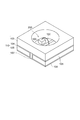
- FIG. 1 is a perspective view showing an embodiment of a substrate for mounting an optical semiconductor element.
- the optical semiconductor element mounting substrate 110 includes a metal wiring 105 (first connection terminal and second connection terminal) on which Ni / Ag plating 104 is formed, and a metal wiring 105 (first connection terminal and second connection terminal). Insulating resin molded body 103 ′ provided between the terminals) and the reflector 103, and formed of the metal wiring 105 formed with the Ni / Ag plating 104 and the insulating resin molded body 103 ′ and the reflector 103.
- An optical semiconductor element mounting region (concave portion) 200 is provided.
- the bottom surface of the recess 200 is composed of the metal wiring 105 on which the Ni / Ag plating 104 is formed and the insulating resin molded body 103 ′, and the wall surface of the recess 200 is composed of the reflector 103.
- the reflector 103 and the insulating resin molded body 103 ′ are molded bodies formed using the thermosetting resin composition of the present embodiment.
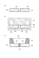
- FIG. 2 is a schematic view showing an embodiment of a process for manufacturing a substrate for mounting an optical semiconductor element.
- the substrate for mounting an optical semiconductor element is formed by, for example, punching from a metal foil, forming a metal wiring 105 by a known method such as etching, and applying Ni / Ag plating 104 by electroplating ((a) in FIG. 2), then The metal wiring 105 is placed in a mold 151 having a predetermined shape, a thermosetting resin composition is injected from the resin injection port 150 of the mold 151, and transfer molding or compression molding is performed under predetermined conditions (FIG. 2). (B)) and can be manufactured through a step of removing the mold 151 ((c) of FIG. 2).
- an optical semiconductor element mounting region (concave portion) 200 is formed on the optical semiconductor element mounting substrate.
- the optical semiconductor element mounting region (concave portion) 200 is surrounded by the reflector 103 made of a cured product of the thermosetting resin composition.
- the bottom surface of the recess 200 has an insulating property made of a cured product of a thermosetting resin composition provided between the metal wiring 105 serving as the first connection terminal and the metal wiring 105 serving as the second connection terminal.
- a resin molded body 103 ′ for example, when the reflector is formed by transfer molding, the molding conditions are a molding temperature of 120 to 200 ° C., a molding pressure of 0.5 to 25 MPa, a pressure of 1 to 3 at an after cure temperature of 120 ° C.
- the mold temperature is more preferably 150 to 190 ° C.
- the molding pressure is more preferably 12 to 20 MPa.
- the molding temperature is 120 to 200 ° C.
- the molding time is 30 to 600 seconds, particularly the molding temperature is 130 to 160 ° C. and the molding time is 120 to 300 seconds. It is preferable to carry out with.
- the color of the reflector 103 is not limited and can be appropriately determined depending on the type of pigment to be used. However, white is preferable from the viewpoint of further increasing the light reflectance.
- the optical semiconductor device includes the optical semiconductor element mounting substrate and an optical semiconductor element mounted on the optical semiconductor element mounting substrate.
- the optical semiconductor element mounting substrate, the optical semiconductor element provided in the recess of the optical semiconductor element mounting substrate, and a sealing resin portion that fills the recess and seals the optical semiconductor element And an optical semiconductor device.
- FIG. 3 is a perspective view showing an embodiment in which the optical semiconductor element 100 is mounted on the optical semiconductor element mounting substrate 110.
- the optical semiconductor element 100 is mounted at a predetermined position in the optical semiconductor element mounting region (concave portion) 200 of the optical semiconductor element mounting substrate 110 and is electrically connected by the metal wiring 105 and the bonding wire 102.
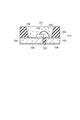
- the 4 and 5 are schematic cross-sectional views showing an embodiment of an optical semiconductor device.
- the optical semiconductor device includes an optical semiconductor element mounting substrate 110, an optical semiconductor element 100 provided at a predetermined position in the concave portion 200 of the optical semiconductor element mounting substrate 110, and the concave portion 200.
- a sealing resin portion made of a transparent sealing resin 101 including a phosphor 106 for sealing the optical semiconductor element, and a metal wiring 105 on which the optical semiconductor element 100 and the Ni / Ag plating 104 are formed. Are electrically connected by a bonding wire 102 or a solder bump 107.
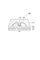
- FIG. 6 is also a schematic cross-sectional view showing an embodiment of an optical semiconductor device.
- the LED element 300 is disposed via a die bonding material 306 at a predetermined position on the lead 304 on which the reflector 303 is formed, and the LED element 300 and the lead 304 are electrically connected by the bonding wire 301.
- the LED element 300 is sealed with a transparent sealing resin 302 that is connected and includes a phosphor 305.
- FIG 5 and 6 show an embodiment of an optical semiconductor device in which one optical semiconductor element is provided, but two or more optical semiconductor elements may be provided in the recess.
- thermosetting resin composition according to this embodiment can be used as a light reflecting resin layer.
- a copper-clad laminate, an optical semiconductor element mounting substrate, and an optical semiconductor element will be described.
- the copper clad laminate according to the present embodiment includes a resin layer formed using the thermosetting resin composition described above, and a copper foil laminated on the resin layer.
- FIG. 7 is a schematic cross-sectional view showing a preferred embodiment of a copper clad laminate.
- the copper-clad laminate 400 includes a base material 401, a resin layer 402 laminated on the base material 401, and a copper foil 403 laminated on the resin layer 402. Yes.
- the resin layer 402 is formed using the thermosetting resin composition of this embodiment mentioned above.
- the base material used for a copper clad laminated board can be used without a restriction
- substrate for optical semiconductor element mounting are mentioned.
- the copper-clad laminate 400 is produced by, for example, forming the resin layer 402 by forming the thermosetting resin composition according to the present embodiment on the surface of the substrate 401, stacking the copper foil 403, and curing by heating and pressing. can do.
- the formation method on the surface of the base material 401 is not limited, and examples thereof include a method of direct application and a method of laminating a resin-coated copper foil containing the thermosetting resin composition according to this embodiment by pressing or laminating.
- the heating and pressing conditions are not particularly limited, but for example, conditions of 130 to 180 ° C., 0.5 to 4 MPa, and 30 to 600 minutes are preferable.
- the copper-clad laminate 400 shown in FIG. 7 is obtained by laminating a resin layer 402 and a copper foil 403 on one side of a base material 401, but the copper clad laminate is a resin layer 402 on both sides of the base material 401. And copper foil 403 may be laminated.
- FIG. 8 is a schematic cross-sectional view showing an example of an optical semiconductor device manufactured using a copper-clad laminate.
- the optical semiconductor device 500 is a surface mount optical semiconductor device including an optical semiconductor element 410 and a sealing resin 404 provided so as to seal the optical semiconductor element 410.
- the optical semiconductor element 410 is bonded to the copper foil 403 through the adhesive layer 408, and is electrically connected to the copper foil 403 by the bonding wire 409.
- an optical semiconductor provided with a resin layer formed between a plurality of conductor members (connection terminals) on a base material using the thermosetting resin composition described above.
- An element mounting substrate may be mentioned.
- the optical semiconductor element is mounted on the optical semiconductor element mounting substrate.
- FIG. 9 is a schematic cross-sectional view showing a preferred embodiment of the optical semiconductor device.
- the optical semiconductor device 600 includes a substrate 601, a plurality of conductor members 602 formed on the surface of the substrate 601, and a resin formed between the plurality of conductor members (connection terminals) 602.
- a surface-mount type optical semiconductor in which an optical semiconductor element 610 is mounted on a substrate for mounting an optical semiconductor element including a layer 603 and a transparent sealing resin 604 is provided so as to seal the optical semiconductor element 610 Device.
- the optical semiconductor element 610 is bonded to the conductor member 602 through the adhesive layer 608, and is electrically connected to the conductor member 602 through a bonding wire 609.
- the resin layer 603 is formed using the thermosetting resin composition described above.
- a base material used for a substrate for mounting an optical semiconductor element can be used without particular limitation, and examples thereof include a resin laminate such as an epoxy resin laminate.
- the conductor member 602 functions as a connection terminal, and can be formed by a known method such as a method of photoetching a copper foil.
- the substrate for mounting an optical semiconductor element is formed by transfer-molding a thermosetting resin composition between a plurality of conductor members 602 on a base material 601, and heat-curing to form a resin layer 603 made of the thermosetting resin composition. Can be produced. There are no particular restrictions on the heating conditions for heat-curing the transfer-molded layer comprising the thermosetting resin composition, but it is preferable to perform heating under conditions of 130 to 200 ° C. and 30 to 600 minutes, for example.
- the conductor member 602 may be subjected to a roughening treatment such as an oxidation-reduction treatment or a CZ treatment (manufactured by MEC Corporation).
- thermosetting resin composition for light reflection According to the blending ratio (parts by mass) shown in Table 1, the respective components were blended and sufficiently kneaded and dispersed at room temperature using a roughing machine to obtain a powdery thermosetting resin composition.
- thermosetting resin composition obtained in each Example was filled with a thermosetting resin composition in a mold having a metal mold having a circular through hole with a diameter of 13 mm as a mortar mold, and a saddle type It was possible to make a tablet shape at room temperature using a punch and a hand press.
- the blending ratio of each component shown in each table is a value excluding the solvent, and the portion indicated by “-” means that the corresponding raw material is not blended.
- the measuring method of each characteristic in the said synthesis example, an Example, and a comparative example is as follows.
- (1) Measurement of weight average molecular weight (Mw) Mw of silicone resin is used as a GPC measuring device with pump “L-6200 type” (trade name, manufactured by Hitachi, Ltd.), columns “TSKgel-G5000HXL” and “TSKgel-G2000HXL”. ”(Trade name, manufactured by Tosoh Corporation) and a detector“ L-3300RI type ”(trade name, manufactured by Hitachi, Ltd.).
- Measurement conditions were such that tetrahydrofuran was used as the eluent, the temperature was 30 ° C., and the flow rate was 1.0 mL / min.
- thermosetting resin compositions obtained in the examples and comparative examples were transfer molded under the conditions of a mold temperature of 180 ° C., a pressure of 14 MPa, and a curing time of 300 seconds, A plate-shaped test piece having a thickness of 3 mm was prepared. The obtained test piece was placed on a 180 ° C. hot plate, allowed to stand for 10 minutes and sufficiently warmed, and according to JIS K 6253-3: 2012, a Type D durometer needle was pressed against the test piece, The value immediately after was measured.
- thermosetting resin compositions obtained in the examples and comparative examples were transfer molded under the conditions of a mold temperature of 180 ° C., a pressure of 14 MPa, and a curing time of 300 seconds, and were 100 mm long ⁇ 20 mm wide.
- X A test piece having a thickness of 4 mm was prepared.
- JIS K 7171: 2008 a three-point bending break test of the obtained test piece was performed at room temperature, and the break strength was measured.
- thermosetting resin composition of an Example since the thermosetting resin composition of an Example has high type D durometer hardness after hardening, it is excellent in toughness, and since the white pigment is used as a pigment, after hardening Is suitable for the production of a substrate for mounting an optical semiconductor element.
- thermosetting resin composition capable of forming a tough cured product that is less likely to crack and crack, a substrate for mounting an optical semiconductor element using the thermosetting resin composition, and a method for manufacturing the same.
- an optical semiconductor device can be provided.
- DESCRIPTION OF SYMBOLS 100 Optical semiconductor element, 101 ... Transparent sealing resin, 102 ... Bonding wire, 103 ... Reflector, 103 '... Insulating resin molding, 104 ... Ni / Ag plating, 105 ... Metal wiring, 106 ... Phosphor, 107 ... Solder bump, 110 ... Optical semiconductor element mounting substrate, 150 ... Resin injection port, 151 ... Mold, 200 ... Optical semiconductor element mounting area, 300 ... LED element, 301 ... Bonding wire, 302 ... Transparent sealing resin, 303 ... Reflector, 304 ... lead, 305 ... phosphor, 306 ... die bond material, 400 ... copper-clad laminate, 401 ...
- substrate 402 ... resin layer, 403 ... copper foil, 404 ... sealing resin, 408 ... adhesive layer, 409 ... Bonding wire, 410 ... Optical semiconductor element, 500, 600 ... Optical semiconductor device, 601 ... Base material, 602 ... Conductive member, 603 ... Fat layer, 604 ... sealing resin, 608 ... adhesive layer, 609 ... bonding wire, 610 ... optical semiconductor element.
Landscapes
- Chemical & Material Sciences (AREA)
- Health & Medical Sciences (AREA)
- Chemical Kinetics & Catalysis (AREA)
- Medicinal Chemistry (AREA)
- Polymers & Plastics (AREA)
- Organic Chemistry (AREA)
- Compositions Of Macromolecular Compounds (AREA)
- Led Device Packages (AREA)
- Non-Metallic Protective Coatings For Printed Circuits (AREA)
- Engineering & Computer Science (AREA)
- Microelectronics & Electronic Packaging (AREA)
- Structures Or Materials For Encapsulating Or Coating Semiconductor Devices Or Solid State Devices (AREA)
Abstract
Description

本実施形態の熱硬化性樹脂組成物は、ヒドロシリル基含有シリコーン樹脂と、アルケニル基当量が50~1000g/molであるアルケニル基含有シリコーン樹脂とを含むシリコーン樹脂及び顔料を含有する。以下、本実施形態の熱硬化性樹脂組成物に含有される各成分について説明する。
ヒドロシリル基含有シリコーン樹脂は、水素原子が直接ケイ素原子に結合した基(Si-H)であるヒドロシリル基を有するシリコーン樹脂であれば特に限定されない。
(GPC条件)
ポンプ:L-6200型(株式会社日立製作所製、商品名)
カラム:TSKgel―G5000HXL及びTSKgel-G2000HXL(東ソー株式会社製、商品名)
検出器:L-3300RI型(株式会社日立製作所製、商品名)
溶離液:テトラヒドロフラン
測定温度:30℃
流量:1.0mL/分
本実施形態の熱硬化性樹脂組成物は、アルケニル基当量が50~1000g/molであるアルケニル基含有シリコーン樹脂を含有する。アルケニル基当量とは、アルケニル基1molを得るのに必要なアルケニル基含有シリコーン樹脂の重量を表す。該アルケニル基は、上述したヒドロシリル基含有シリコーン樹脂が有するヒドロシリル基と、好ましくは硬化触媒の存在下、付加反応することで熱硬化性樹脂組成物の硬化物を形成することができる。アルケニル基当量が上記範囲内であれば、硬化後の樹脂の構造は架橋密度の高いものとなる。
Y=MI2×100/X


反応性の観点から、本実施形態の樹脂組成物中にはシリコーン樹脂のヒドロシリル化反応を促進する硬化触媒を含有することが好ましい。硬化触媒としては、例えば、カルステッド触媒;白金の単体;担体(アルミナ、シリカ、カーボンブラック等)に固体白金を担持させたもの;塩化白金酸;塩化白金酸とアルコール、アルデヒド、ケトン等との錯体;白金-オレフィン錯体;白金-ビニルシロキサン錯体;白金-ホスフィン錯体;白金-ホスファイト錯体及びジカルボニルジクロロ白金が挙げられる。これらの硬化触媒は単独で使用してもよく、2種以上併用してもよい。
顔料は、本実施形態にかかる熱硬化性樹脂組成物の硬化物に用途に応じた色を付加する。本実施形態に係る顔料は、作製される熱硬化性樹脂組成物の硬化物の使用目的に応じて選択することができる。顔料としては、例えば、白色顔料、黒色顔料、赤色顔料、黄色顔料、橙色顔料、紫(菫)色顔料、青色顔料及び緑色顔料が挙げられる。顔料は、アゾ顔料、レーキ顔料又は蛍光顔料であってもよい。
熱硬化性樹脂組成物は、上述した成分以外に、無機充填剤、カップリング剤、硬化遅延剤、シリコーン樹脂以外の熱硬化性樹脂、酸化防止剤、離型剤、分散剤、イオン捕捉剤等の各種添加剤を更に含有することができる。
本実施形態の熱硬化性樹脂組成物を光反射材料として用いる場合、硬化後の光反射率が、波長440~700nmのいずれかにおいて80%以上となることが好ましい。光反射率が80%以上であれば、光半導体装置の輝度をより向上できる。また、青色発光ダイオードを用いた光半導体装置に好適とする観点から、硬化後の波長460nmにおける光反射率が、80%以上となることが好ましく、90%以上となることがより好ましい。
本実施形態に係る熱硬化性樹脂組成物の製造方法は特に限定されないが、例えば、以下のような混練工程及び粉砕工程を備えていてもよい。
熱硬化性樹脂組成物は、先に例示した各種成分を均一に分散混合することによって調製することができ、混合手段、混合条件等は特に制限されない。調製方法としては、例えば、ミキシングロール、押出機、ニーダー、ロール、エクストルーダー、らいかい機、自転と公転を組み合わせた攪拌混合機等の装置を用いて各種成分を混練する方法が挙げられる。混練形式についても特に限定されないが、作業が容易な観点から溶融混練とすることが好ましく、工程の簡略化の観点から、混練は15~30℃で実施されることが好ましい。加熱を要する際は、例えば、30~100℃の温度範囲であってもよい。溶融混練の温度が30℃以上であると、各種成分をより十分に溶融混練することが可能であり、分散性がより向上する傾向がある。一方、溶融混練を100℃以下で実施すると、樹脂組成物の高分子量化をより抑制でき、基板等の成形品を成形する前に樹脂組成物が硬化してしまうことをより抑制できる。混錬時間は5~40分間であってもよく、10~30分間であってもよい。溶融混練の時間が5分間以上であると、基板等の成形時に金型から樹脂が染み出すことをより抑制でき、40分間以内であると、樹脂組成物の高分子化を制御し易く、成形前に樹脂組成物が硬化することをより抑制できる。
粉砕工程では、例えば、熱硬化性樹脂組成物を乾式粉砕する。乾式粉砕は、例えば、高速攪拌ミル、ヘンシェルミキサ、パワーミル、ジェットミル、ロールグラニュレータ等の粉砕装置を用いて行うことができる。これらの粉砕装置は、目的の粉末粒径により使い分けることができる。
本実施形態の硬化物は、上述の熱硬化性樹脂組成物を熱硬化させることで形成することができる。熱硬化の条件は特に限定はないが、例えば、温度170~200℃で、60~300秒間加熱することにより硬化できる。熱硬化は後述の成形法に含まれる工程の一部として行ってもよい。
本実施形態に係る光半導体素子搭載用基板は、底面及び壁面から構成される凹部を有する。凹部の底面が光半導体素子搭載部(光半導体素子搭載領域)であり、凹部の壁面、すなわち凹部の内周側面の少なくとも一部が本実施形態の熱硬化性樹脂組成物から形成された成形体からなるものである。
本実施形態に係る光半導体装置は、上記光半導体素子搭載用基板と、当該光半導体素子搭載用基板に搭載された光半導体素子とを有する。より具体的な例として、上記光半導体素子搭載用基板と、光半導体素子搭載用基板の凹部内に設けられた光半導体素子と、凹部を充填して光半導体素子を封止する封止樹脂部とを備える光半導体装置が挙げられる。
フェニルトリクロロシラン100g、両末端ジメチルクロロシラン-ポリジメチルシロキサン53g、及びメチルジクロロシラン6.9gをトルエンに溶解した溶液を、発熱しないように水1000g中に滴下し加水分解した。次いで、還流条件で60分攪拌した後、有機層を水酸化カリウムで中和し、共沸脱水後、トルエン等の溶剤を留去し、無色透明のヒドロシリル基含有シリコーン樹脂を得た。得られたヒドロシリル基含有シリコーン樹脂のMwは3865であった。
ビニルトリメトキシシラン53.5g、メチルトリエトキシシラン1.2g、イソプロピルアルコール60g、トルエン120g、濃塩酸0.59g及び蒸留水15.9gを500mLフラスコに加えて、170℃で2時間にわたって還流しながら攪拌した。次にトルエンを減圧留去し、アルケニル基含有シリコーン樹脂を得た。得られたアルケニル基含有シリコーン樹脂のMwは2300であり、Siに直接結合した元素の全量を基準としたアルケニル基含有量は24モル%であり、Siに直接結合した有機基の全量を基準としたアルケニル基含有量は98モル%であり、アルケニル基当量は150g/molであった。アルケニル基含有シリコーン樹脂は50質量%のアセトン溶液として保存した。
ビニルトリメトキシシラン425g、イソプロピルアルコール120g、トルエン240g、濃塩酸1.18g及び蒸留水31.4gを1000mLフラスコに加えて、170℃で時間にわたって還流しながら攪拌した。次にトルエンを減圧留去し、アルケニル基含有シリコーン樹脂を得た。得られたアルケニル基含有シリコーン樹脂のMwは4000であり、Siに直接結合した元素の全量を基準としたアルケニル基含有量は25モル%であり、Siに直接結合した有機基の全量を基準としたアルケニル基含有量は100モル%であり、アルケニル基当量は85g/molであった。アルケニル基含有シリコーン樹脂は50質量%のアセトン溶液として保存した。
フェニルトリクロロシラン100g、両末端ジメチルクロロシラン-ポリジメチルシロキサン53g及びメチルビニルジクロロシラン8.5gをトルエン200gに溶解した溶液を、発熱しないように水1000g中に滴下し加水分解した。次いで、還流条件で60分攪拌した後、有機層を水酸化カリウムで中和し、共沸脱水後、トルエン等の溶剤を留去し、無色液状のアルケニル基含有シリコーン樹脂を得た。得られたアルケニル基含有シリコーン樹脂のMwは3685であり、アルケニル基当量は1585g/molであった。
メチルトリエトキシシラン89.2g、フェニルトリエトキシシラン99g、イソプロピルアルコール23.6g、トルエン23.6g、濃塩酸0.28g及び蒸留水36gを500mLフラスコに加えて、110℃で3時間にわたって還流しながら攪拌した。次に、トルエンを減圧留去することにより無色固形のシリコーン樹脂を得た。得られたシリコーン樹脂のMwは901であった。
メチルトリエトキシシラン142.6g、フェニルトリエトキシシラン39.7g、イソプロピルアルコール22.8g、トルエン22.8g、濃塩酸0.28g及び蒸留水36gを500mLフラスコに加えて、110℃で2.5時間にわたって還流しながら攪拌した。次に、トルエンを減圧留去することにより無色固形のシリコーン樹脂を得た。得られたシリコーン樹脂のMwは1300であった。
(実施例)
表1に示す配合割合(質量部)に従って、各成分を配合し、らいかい機によって室温で十分に混練分散することによって粉末状の熱硬化性樹脂組成物を得た。なお、各実施例にて得られた熱硬化性樹脂組成物は、直径13mmの円形貫通穴を有する金属金型を臼型とする成形型に、熱硬化性樹脂組成物を充填し、杵型のパンチとハンドプレスとを用いて、常温でタブレット形状とすることが可能であった。
表2に示す配合割合(質量部)に従って、各成分を配合し、らいかい機によって室温で十分に混練分散することによって粉末状の熱硬化性樹脂組成物を得た。


*1:ヒドロシリル基含有シリコーン樹脂(合成例1)
*2:アルケニル基含有シリコーン樹脂(合成例2)
*3:アルケニル基含有シリコーン樹脂(合成例3)
*4:アルケニル基含有シリコーン樹脂(合成例4)
*5:シリコーン樹脂(合成例5)
*6:シリコーン樹脂(合成例6)
*7:白金(0)-2,4,6,8-テトラメチル-2,4,6,8-テトラビニルシクロテトラシロキサン錯体(和光純薬工業株式会社製、白金1.7質量%)
*8:溶融シリカ(電気化学工業株式会社製、商品名「FB-950」、中心粒径26μm)
*9:溶融シリカ(株式会社アドマテックス製、商品名「SO-25R」、中心粒径1μm)
*10:中空粒子(ソーダ石灰硼珪酸ガラス、住友スリーエム株式会社製、商品名「S60-HS」、中心粒径27μm)
*11:酸化チタン(石原産業株式会社製、商品名「CR63」、中心粒径0.2μm)
(1)重量平均分子量(Mw)の測定
シリコーン樹脂のMwを、GPC測定装置としてポンプ「L-6200型」(株式会社日立製作所製、商品名)、カラム「TSKgel―G5000HXL」及び「TSKgel-G2000HXL」(東ソー株式会社製、商品名)及び検出器「L-3300RI型」(株式会社日立製作所製、商品名)を用いて測定した。測定条件は、溶離液としてテトラヒドロフランを使用し、温度30℃、流量1.0mL/分とした。
「FT-NMR AV400M」(ブルカー・バイオスピン株式会社製、商品名)を用いて、シリコーン樹脂の1H-NMR測定を行い、シリコーン樹脂中のアルケニル基及びアルキル基の含有量を測定した。測定条件は、シリコーン樹脂を0.5質量%含むように調整した重クロロホルム溶液を用い、積算回数(NS)を32とした。
JIS K 0070:1992に従い、ヨウ素価を測定した。測定されたヨウ素価及び(1)にて測定した重量平均分子量からアルケニル基当量を算出した。
実施例及び比較例でそれぞれ得られた熱硬化性樹脂組成物を、金型温度180℃、圧力14MPa、硬化時間300秒の条件でトランスファー成形し、厚み3mmのプレート状の試験片を作製した。得られた試験片を180℃のホットプレート上に乗せて10分間静置させて十分に温めた後、JIS K 6253-3:2012に準じて、タイプDデュロメータの針を試験片に押しあて、直後の値を測定した。
実施例及び比較例でそれぞれ得られた熱硬化性樹脂組成物を、金型温度180℃、圧力14MPa、硬化時間300秒の条件でトランスファー成形し、縦100mm×横20mm×厚み4mmの試験片を作製した。JIS K 7171:2008に準じて、得られた試験片の三点曲げ破断試験を室温で行ない、破断強度を測定した。
(4)で作製した試験片について、積分球型分光硬度計CM600d(コニタミノルタ株式会社製)を用いて、波長460nmにおける光反射率を測定した。
Claims (13)
- ヒドロシリル基含有シリコーン樹脂と、アルケニル基当量が50~1000g/molであるアルケニル基含有シリコーン樹脂とを含むシリコーン樹脂及び顔料を含有する、熱硬化性樹脂組成物。
- 前記アルケニル基含有シリコーン樹脂が、ケイ素原子に結合する有機基の全量を基準としてアルケニル基を75モル%以上有する、請求項1に記載の熱硬化性樹脂組成物。
- 前記アルケニル基含有シリコーン樹脂の重量平均分子量が200~10000である、請求項1又は2に記載の熱硬化性樹脂組成物。
- 前記アルケニル基含有シリコーン樹脂が、下記式(I)で表される構造を有する、請求項1~3のいずれか一項に記載の熱硬化性樹脂組成物。
- 当該熱硬化性樹脂組成物の全量を基準として、前記アルケニル基含有シリコーン樹脂を0.0005~35質量%含む、請求項1~4のいずれか一項に記載の熱硬化性樹脂組成物。
- 前記顔料が、酸化チタン、酸化亜鉛、アルミナ、酸化マグネシウム、酸化アンチモン及び酸化ジルコニウムからなる群より選ばれる少なくとも1種の白色顔料を含む、請求項1~5のいずれか一項に記載の熱硬化性樹脂組成物。
- 前記顔料が中空粒子を含有する、請求項1~6のいずれか一項に記載の熱硬化性樹脂組成物。
- タブレット状である、請求項1~7のいずれか一項に記載の熱硬化性樹脂組成物。
- 請求項1~8のいずれか一項に記載の熱硬化性樹脂組成物から形成される、硬化物。
- 底面及び壁面から構成される凹部を有し、当該凹部の前記底面が光半導体素子の搭載部であり、前記凹部の前記壁面の少なくとも一部に請求項1~8のいずれか一項に記載の熱硬化性樹脂組成物から形成された成形体を有する、光半導体素子搭載用基板。
- 基板と、当該基板上に設けられた第1の接続端子及び第2の接続端子とを備え、
前記第1の接続端子と前記第2の接続端子との間に、請求項1~8のいずれか一項に記載の熱硬化性樹脂組成物から形成された成形体を有する、光半導体素子搭載用基板。 - 請求項10又は11に記載の光半導体素子搭載用基板と、当該光半導体素子搭載用基板に搭載された光半導体素子と、を備える、光半導体装置。
- 底面及び壁面から構成される凹部を有する光半導体素子搭載用基板の製造方法であって、
前記凹部の前記壁面の少なくとも一部を、請求項1~8のいずれか一項に記載の熱硬化性樹脂組成物を用いてトランスファー成形又はコンプレッション成形して形成する工程を備える、光半導体素子搭載用基板の製造方法。
Priority Applications (4)
| Application Number | Priority Date | Filing Date | Title |
|---|---|---|---|
| PCT/JP2016/060472 WO2017168649A1 (ja) | 2016-03-30 | 2016-03-30 | 熱硬化性樹脂組成物、光半導体素子搭載用基板及びその製造方法並びに光半導体装置 |
| JP2018507952A JP6566121B2 (ja) | 2016-03-30 | 2016-03-30 | 熱硬化性樹脂組成物、光半導体素子搭載用基板及びその製造方法並びに光半導体装置 |
| CN201680084083.4A CN109075229B (zh) | 2016-03-30 | 2016-03-30 | 热固化性树脂组合物、光半导体元件搭载用基板及其制造方法、以及光半导体装置 |
| KR1020187028370A KR20180128921A (ko) | 2016-03-30 | 2016-03-30 | 열경화성 수지 조성물, 광 반도체 소자 탑재용 기판 및 그의 제조 방법 및 광 반도체 장치 |
Applications Claiming Priority (1)
| Application Number | Priority Date | Filing Date | Title |
|---|---|---|---|
| PCT/JP2016/060472 WO2017168649A1 (ja) | 2016-03-30 | 2016-03-30 | 熱硬化性樹脂組成物、光半導体素子搭載用基板及びその製造方法並びに光半導体装置 |
Publications (1)
| Publication Number | Publication Date |
|---|---|
| WO2017168649A1 true WO2017168649A1 (ja) | 2017-10-05 |
Family
ID=59963668
Family Applications (1)
| Application Number | Title | Priority Date | Filing Date |
|---|---|---|---|
| PCT/JP2016/060472 Ceased WO2017168649A1 (ja) | 2016-03-30 | 2016-03-30 | 熱硬化性樹脂組成物、光半導体素子搭載用基板及びその製造方法並びに光半導体装置 |
Country Status (4)
| Country | Link |
|---|---|
| JP (1) | JP6566121B2 (ja) |
| KR (1) | KR20180128921A (ja) |
| CN (1) | CN109075229B (ja) |
| WO (1) | WO2017168649A1 (ja) |
Citations (4)
| Publication number | Priority date | Publication date | Assignee | Title |
|---|---|---|---|---|
| JP2013035894A (ja) * | 2011-08-04 | 2013-02-21 | Nitto Denko Corp | シリコーン樹脂組成物、封止材料および発光ダイオード装置 |
| JP2013221077A (ja) * | 2012-04-16 | 2013-10-28 | Shin-Etsu Chemical Co Ltd | Ledのリフレクター用熱硬化性シリコーン樹脂組成物並びにこれを用いたled用リフレクター及び光半導体装置 |
| JP2014129549A (ja) * | 2010-03-23 | 2014-07-10 | Asahi Rubber Inc | シリコーン樹脂製反射基材、その製造方法、及びその反射基材に用いる原材料組成物 |
| JP2015109337A (ja) * | 2013-12-04 | 2015-06-11 | 日東電工株式会社 | 光半導体装置用熱硬化性樹脂組成物およびそれを用いて得られる光半導体装置用リードフレーム、ならびに光半導体装置 |
Family Cites Families (2)
| Publication number | Priority date | Publication date | Assignee | Title |
|---|---|---|---|---|
| EP2062601A4 (en) * | 2006-09-11 | 2012-07-25 | Kaneka Corp | FOAM AND PROCESS FOR PRODUCING THE SAME |
| JP5830201B2 (ja) * | 2013-08-06 | 2015-12-09 | 株式会社ダイセル | 硬化性樹脂組成物及びそれを用いた半導体装置 |
-
2016
- 2016-03-30 KR KR1020187028370A patent/KR20180128921A/ko not_active Withdrawn
- 2016-03-30 JP JP2018507952A patent/JP6566121B2/ja active Active
- 2016-03-30 CN CN201680084083.4A patent/CN109075229B/zh active Active
- 2016-03-30 WO PCT/JP2016/060472 patent/WO2017168649A1/ja not_active Ceased
Patent Citations (4)
| Publication number | Priority date | Publication date | Assignee | Title |
|---|---|---|---|---|
| JP2014129549A (ja) * | 2010-03-23 | 2014-07-10 | Asahi Rubber Inc | シリコーン樹脂製反射基材、その製造方法、及びその反射基材に用いる原材料組成物 |
| JP2013035894A (ja) * | 2011-08-04 | 2013-02-21 | Nitto Denko Corp | シリコーン樹脂組成物、封止材料および発光ダイオード装置 |
| JP2013221077A (ja) * | 2012-04-16 | 2013-10-28 | Shin-Etsu Chemical Co Ltd | Ledのリフレクター用熱硬化性シリコーン樹脂組成物並びにこれを用いたled用リフレクター及び光半導体装置 |
| JP2015109337A (ja) * | 2013-12-04 | 2015-06-11 | 日東電工株式会社 | 光半導体装置用熱硬化性樹脂組成物およびそれを用いて得られる光半導体装置用リードフレーム、ならびに光半導体装置 |
Also Published As
| Publication number | Publication date |
|---|---|
| JPWO2017168649A1 (ja) | 2019-02-07 |
| CN109075229A (zh) | 2018-12-21 |
| KR20180128921A (ko) | 2018-12-04 |
| JP6566121B2 (ja) | 2019-08-28 |
| CN109075229B (zh) | 2021-03-19 |
Similar Documents
| Publication | Publication Date | Title |
|---|---|---|
| TWI575053B (zh) | 光反射性異向性導電接著劑及發光裝置 | |
| KR101575209B1 (ko) | 열경화성 수지 조성물, 에폭시 수지 성형 재료 및 다가 카르복시산 축합체 | |
| JP4586925B2 (ja) | 熱硬化性樹脂組成物、エポキシ樹脂成形材料、光半導体素子搭載用基板及びその製造方法、並びに光半導体装置 | |
| JP5942445B2 (ja) | 光反射用熱硬化性樹脂組成物、これを用いた光半導体素子搭載用基板及びその製造方法、並びに光半導体装置 | |
| CN103154072B (zh) | 固化性环氧树脂组合物 | |
| JP6988107B2 (ja) | 熱硬化性樹脂組成物の製造方法、光半導体素子搭載用基板の製造方法、光半導体装置の製造方法及び熱硬化性樹脂組成物 | |
| JP6343552B2 (ja) | 光反射用熱硬化性樹脂組成物、これを用いた光半導体素子搭載用基板及びその製造方法、並びに光半導体装置 | |
| TW201418407A (zh) | 光反射性異向性導電接著劑及發光裝置 | |
| JP2010254919A (ja) | 光反射用熱硬化性樹脂組成物、これを用いた光半導体素子搭載用基板及びその製造方法、並びに光半導体装置 | |
| JP5936804B2 (ja) | 熱硬化性樹脂組成物、光半導体素子搭載用基板及びその製造方法、並びに光半導体装置 | |
| JP6805546B2 (ja) | 熱硬化性樹脂組成物、硬化物、光半導体素子搭載用基板及びその製造方法、光半導体装置、並びにプリント配線板 | |
| JP5401905B2 (ja) | 熱硬化性樹脂組成物 | |
| JP6566121B2 (ja) | 熱硬化性樹脂組成物、光半導体素子搭載用基板及びその製造方法並びに光半導体装置 | |
| JP6322929B2 (ja) | 光反射用熱硬化性樹脂組成物、光半導体素子搭載用基板及びその製造方法、並びに光半導体装置 | |
| JP6672631B2 (ja) | シリコーン樹脂タブレット、光半導体素子搭載用基板及びその製造方法、並びに、光半導体装置 | |
| JP2012162729A (ja) | 光反射用熱硬化性樹脂組成物、これを用いた光半導体素子搭載用基板及びその製造方法、並びに光半導体装置 | |
| JP2016028426A (ja) | 光反射用熱硬化性樹脂組成物、これを用いた光半導体素子搭載用基板及びその製造方法、並びに光半導体装置 | |
| JP2015017271A (ja) | 熱硬化性樹脂組成物、光半導体素子搭載用基板及びその製造方法、並びに光半導体装置 | |
| JP2017147454A (ja) | 光反射用熱硬化性樹脂組成物の製造方法及び光半導体素子搭載用基板の製造方法 | |
| JP2014195081A (ja) | 光反射用熱硬化性樹脂組成物、これを用いた光半導体素子搭載用基板及びその製造方法、並びに光半導体装置 |
Legal Events
| Date | Code | Title | Description |
|---|---|---|---|
| WWE | Wipo information: entry into national phase |
Ref document number: 2018507952 Country of ref document: JP |
|
| ENP | Entry into the national phase |
Ref document number: 20187028370 Country of ref document: KR Kind code of ref document: A |
|
| NENP | Non-entry into the national phase |
Ref country code: DE |
|
| 121 | Ep: the epo has been informed by wipo that ep was designated in this application |
Ref document number: 16896868 Country of ref document: EP Kind code of ref document: A1 |
|
| 122 | Ep: pct application non-entry in european phase |
Ref document number: 16896868 Country of ref document: EP Kind code of ref document: A1 |