WO2017164059A1 - アンテナ - Google Patents
アンテナ Download PDFInfo
- Publication number
- WO2017164059A1 WO2017164059A1 PCT/JP2017/010646 JP2017010646W WO2017164059A1 WO 2017164059 A1 WO2017164059 A1 WO 2017164059A1 JP 2017010646 W JP2017010646 W JP 2017010646W WO 2017164059 A1 WO2017164059 A1 WO 2017164059A1
- Authority
- WO
- WIPO (PCT)
- Prior art keywords
- antenna
- unit
- antenna unit
- substrate layer
- region
- Prior art date
- Legal status (The legal status is an assumption and is not a legal conclusion. Google has not performed a legal analysis and makes no representation as to the accuracy of the status listed.)
- Ceased
Links
Images





Classifications
-
- H—ELECTRICITY
- H01—ELECTRIC ELEMENTS
- H01Q—ANTENNAS, i.e. RADIO AERIALS
- H01Q5/00—Arrangements for simultaneous operation of antennas on two or more different wavebands, e.g. dual-band or multi-band arrangements
- H01Q5/30—Arrangements for providing operation on different wavebands
- H01Q5/378—Combination of fed elements with parasitic elements
-
- H—ELECTRICITY
- H01—ELECTRIC ELEMENTS
- H01Q—ANTENNAS, i.e. RADIO AERIALS
- H01Q13/00—Waveguide horns or mouths; Slot antennas; Leaky-waveguide antennas; Equivalent structures causing radiation along the transmission path of a guided wave
- H01Q13/10—Resonant slot antennas
-
- H—ELECTRICITY
- H01—ELECTRIC ELEMENTS
- H01Q—ANTENNAS, i.e. RADIO AERIALS
- H01Q5/00—Arrangements for simultaneous operation of antennas on two or more different wavebands, e.g. dual-band or multi-band arrangements
- H01Q5/30—Arrangements for providing operation on different wavebands
- H01Q5/307—Individual or coupled radiating elements, each element being fed in an unspecified way
- H01Q5/314—Individual or coupled radiating elements, each element being fed in an unspecified way using frequency dependent circuits or components, e.g. trap circuits or capacitors
- H01Q5/321—Individual or coupled radiating elements, each element being fed in an unspecified way using frequency dependent circuits or components, e.g. trap circuits or capacitors within a radiating element or between connected radiating elements
-
- H—ELECTRICITY
- H01—ELECTRIC ELEMENTS
- H01Q—ANTENNAS, i.e. RADIO AERIALS
- H01Q5/00—Arrangements for simultaneous operation of antennas on two or more different wavebands, e.g. dual-band or multi-band arrangements
- H01Q5/30—Arrangements for providing operation on different wavebands
- H01Q5/378—Combination of fed elements with parasitic elements
- H01Q5/385—Two or more parasitic elements
-
- H—ELECTRICITY
- H01—ELECTRIC ELEMENTS
- H01Q—ANTENNAS, i.e. RADIO AERIALS
- H01Q7/00—Loop antennas with a substantially uniform current distribution around the loop and having a directional radiation pattern in a plane perpendicular to the plane of the loop
-
- H—ELECTRICITY
- H01—ELECTRIC ELEMENTS
- H01Q—ANTENNAS, i.e. RADIO AERIALS
- H01Q1/00—Details of, or arrangements associated with, antennas
- H01Q1/36—Structural form of radiating elements, e.g. cone, spiral, umbrella; Particular materials used therewith
- H01Q1/38—Structural form of radiating elements, e.g. cone, spiral, umbrella; Particular materials used therewith formed by a conductive layer on an insulating support
-
- H—ELECTRICITY
- H01—ELECTRIC ELEMENTS
- H01Q—ANTENNAS, i.e. RADIO AERIALS
- H01Q1/00—Details of, or arrangements associated with, antennas
- H01Q1/48—Earthing means; Earth screens; Counterpoises
-
- H—ELECTRICITY
- H01—ELECTRIC ELEMENTS
- H01Q—ANTENNAS, i.e. RADIO AERIALS
- H01Q9/00—Electrically-short antennas having dimensions not more than twice the operating wavelength and consisting of conductive active radiating elements
- H01Q9/04—Resonant antennas
- H01Q9/30—Resonant antennas with feed to end of elongated active element, e.g. unipole
- H01Q9/42—Resonant antennas with feed to end of elongated active element, e.g. unipole with folded element, the folded parts being spaced apart a small fraction of the operating wavelength
Definitions
- the present invention relates to an antenna.
- the present invention particularly relates to a thin antenna having good characteristics that resonates in a plurality of frequency bands.
- the present invention is intended to solve the problems associated with the prior art as described above, and an object of the present invention is to provide a thinner multiband antenna.
- a linear first antenna unit a conduction unit that connects the first antenna unit and a feeding point, a region that short-circuits both ends of the first antenna unit and grounds
- An antenna is provided that includes a second antenna unit that is disposed in a region surrounded by the region and the first antenna unit, at least a part of which overlaps with the conductive unit across the conductive unit and the dielectric.
- a linear first antenna unit a conduction unit that connects the first antenna unit and a feeding point, a region that short-circuits both ends of the first antenna unit and grounds, (N-1) arranged in a region defined by the relationship between the first antenna unit, the conducting unit and the region so as to resonate with the first antenna unit at n frequencies (n is 2 or more).
- An antenna comprising a plurality of second antenna portions is provided.
- a thinner multiband antenna can be provided.
- FIG. 1 is a configuration diagram of an antenna according to an embodiment of the present invention.
- FIG. 2 is a diagram showing a substrate layer configuration of an antenna according to an embodiment of the present invention.
- the antenna 1 includes a first antenna unit 11, a conduction unit 12, a second antenna unit 13, a feeding point 14, a ground 15, and a derivative substrate 16.
- the antenna has three substrate layers, and includes a first substrate layer L1, a second substrate layer L2, and a third substrate layer L3.
- the first antenna unit 11 is a planar antenna created by printing on the dielectric substrate 16.
- the shape of the first antenna unit 11 is linear.
- the term “linear” refers to a shape having a width rather than being elongated and having no width.
- the width may be a constant width in all of the first antenna parts 61 as shown in FIG. 6, or may be a different width for each location as shown in FIG.
- the symbol 11L means the left end portion of the first antenna unit 11, and the symbol 11R means the right end portion of the first antenna unit 11.
- the left end and the right end are collectively referred to as both ends.
- the first antenna unit 11 is disposed on the first substrate layer L1.
- the 1st antenna part 11 has antenna return parts 11a and 11b.
- the linear part 11c of the 1st antenna part 11 is connected to the antenna folding
- a direction horizontal to the straight line portion 11c of the first antenna unit 11 is defined as an x direction
- a vertical direction is defined as a y direction.
- the antenna folded portions 11a and 11b are formed so as to be long in the y direction and short in the x direction. As a result, the first antenna unit 11 can be formed short in the x direction.
- the length from the left end 11L to the right end 11R of the first antenna unit 11 has a correlation with the resonance frequency. Therefore, the antenna can be further reduced in size when the antenna folding portion is provided than when the antenna folding portion is not provided.
- the conducting part 12 connects the first antenna part 11 and the feeding point 14.
- the conduction unit 12 is connected to the first antenna unit 11 at a midpoint between both ends of the first antenna unit 11.
- the position of the conducting part 12 is not limited to the position where it is connected to the first antenna part 11 at the midpoint between both ends of the first antenna part 11.
- the conduction portion 12 is formed in the same layer as the first antenna portion 11.
- the second antenna unit 13 is a parasitic element. However, in order to generate a new resonance point by the parasitic element, it is necessary to arrange the second antenna unit 13 at a position affected by the conduction unit 12.
- the conducting part 12 may be at a position where at least a part of the conducting part 12 overlaps with the second antenna part 13 with the dielectric interposed therebetween.
- the conduction part 12 is connected to the first antenna part 11 at a position shifted from the midpoint between both ends of the first antenna part 11, the radiation pattern does not exhibit non-directionality.
- the conduction unit 12 is connected to the first antenna unit 11 at a midpoint between both ends of the first antenna unit 11.
- the conducting portion 12 has a narrow end connected to the feeding point 14 in order to finely adjust the characteristic impedance of the antenna.
- the ground 15 is formed in a region where both ends of the first antenna unit 11 are short-circuited and grounded.
- the first antenna unit 11 is connected to the ground 15 and operates in a loop shape. Since both ends of the first antenna unit 11 are connected to the left and right sides of the ground 15, the current distribution does not spread over the entire ground 15, but is concentrated in a region near the first antenna unit 11.
- the second antenna unit 13 is arranged so that at least a part of the second antenna unit 13 overlaps the conduction unit 12 with the conduction unit 12 and a dielectric (not shown) arranged as the second substrate layer L2 interposed therebetween. Further, the second antenna unit 13 is disposed in a region formed by the ground 15 and the first antenna unit 11. That is, the second antenna unit 13 does not overlap the first antenna unit 11 and the ground 15 with a dielectric interposed therebetween.
- the second antenna unit 13 is defined by the relationship between the first antenna unit 11, the conduction unit 12, the ground 15, and the region formed by the first antenna unit 11 so as to resonate with the first antenna unit 11 at a plurality of frequencies. Placed in the area. In this example, the second antenna unit 13 is disposed on the third substrate layer L3.
- the second antenna unit 13 is not connected to a feeding point and is a parasitic antenna element.
- the second antenna unit 13 In order to transmit radio waves from the second antenna unit 13, it is necessary to receive a high frequency current through the second antenna unit 13 due to the influence of the conduction unit 12. Therefore, the second antenna unit 13 must be arranged at a certain distance from the conducting unit 12. On the other hand, if the second antenna unit 13 is too close to the conducting unit 12, the frequency characteristics of VSWR (Voltage Standing Wave Ratio) will deteriorate.
- VSWR Voltage Standing Wave Ratio
- the second antenna portion 13 is formed in the shape of the antenna shown in FIGS. 3A and 3B.
- the distance between the plane and the plane on which the conductive portion 12 is formed was moved. When this distance was moved, it was confirmed whether or not the characteristic impedance was adjusted near 2.5 GHz and 5 GHz as shown in FIG. 4, and the range where this adjustment was taken was obtained.
- the distance between the plane on which the second antenna portion 13 is formed and the plane on which the conductive portion 12 is formed is ⁇ / 250 or more and ⁇ / 25 or less with respect to the resonance frequency of the first antenna.
- the second antenna unit 13 has a T shape for impedance optimization.
- the shape of the second antenna unit 13 is not limited to this, and the shape of the second antenna unit 13 is a rectangle or the like as long as it can transmit and receive two desired frequencies together with the first antenna unit 11. Also good.
- the antenna has three substrate layers including a first substrate layer L1, a second substrate layer L2, and a third substrate layer L3.
- the first substrate layer L1 includes the first antenna unit 11 and the ground 15.
- the second substrate layer L2 includes a dielectric.
- the dielectric material of the second substrate layer L2 is not limited to the glass epoxy FR4, and may be a Teflon (registered trademark) substrate or the like.
- the dielectric of the second substrate layer L2 may be air. In the case of air, there is a space between the first substrate layer L1 and the die 3 substrate layer L3.
- the relative dielectric constant is large, the wavelength is shortened and the thickness of the second substrate layer L2 is also thinned.
- glass epoxy FR4 has a larger dielectric constant than air. Therefore, the glass epoxy FR4 has an effect that the thickness of the second substrate layer L2 becomes thinner than the case where the dielectric is air.
- the third substrate layer L3 includes the second antenna unit 13 and ground (not shown).
- the ground has the same shape and size as the ground 15 of the first substrate layer L1, as shown by the ground 17 in FIG. 3B.
- the ground 17 may not be provided.
- 3A and 3B are diagrams for explaining a simulation situation for confirming the VSWR frequency characteristic and the radiation pattern of the antenna according to the embodiment of the present invention.
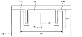
- FIG. 3A is a view as seen from the first substrate layer L1 side.
- the first antenna unit 11, the conduction unit 12, the feeding point 14, and the ground 15 are arranged.
- a dielectric is disposed on the second substrate layer L2.
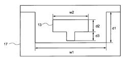
- FIG. 3B is a view from the third substrate layer L3 side.
- the second antenna unit 13 and the ground 17 are disposed on the third substrate layer L3.
- the length w1 between both ends of the first antenna unit 11 is 35 mm, and the vertical length d1 of the ground 15 is 14 mm.
- the thickness of the second substrate layer L2 of the antenna is 0.6 mm.
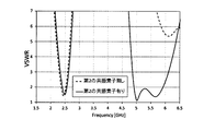
- FIG. 4 is a simulation result showing the VSWR frequency characteristics of the antenna according to the embodiment of the present invention.
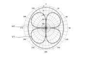
- FIG. 5 is a simulation result for confirming the radiation pattern of the antenna according to the embodiment of the present invention.
- FIG. 4 indicates the VSWR when the first antenna unit 11 is provided but the second antenna unit (second resonance element) 13 is not provided.
- the solid line in FIG. 4 indicates the first antenna unit (first resonance unit).
- the VSWR when there is a second antenna portion (second resonant element) 13 in addition to the element 11 is shown.
- the value of VSWR is close to 1 near 2.5 GHz, whereas 5 In the vicinity of ⁇ 6 GHz, the value of VSWR is away from 1.
- the value of VSWR is close to 1 near 2.5 GHz and 5 GHz. It can be seen that the efficiency of the antenna radiating electric energy is the best around 2.5 GHz and 5 GHz. That is, the characteristic impedance is adjusted around 2.5 GHz and 5 GHz.
- the simulation target antenna is a dual-band antenna that functions as an antenna in two frequency bands near 2.5 GHz and 5 GHz even if the thickness of the second substrate layer L2 of the antenna is 0.6 mm. You can say that.
- FIG. 5A is a diagram showing a radiation pattern (2.4 GHz band) by the first antenna unit 11.
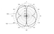
- FIG. 5B is a diagram illustrating a radiation pattern (5 GHz band) at a resonance point generated by adding the second antenna unit 13 to the first antenna unit 11.
- H1 (broken line) in FIG. 5A indicates the gain of horizontal polarization
- V1 (solid line) in FIG. 5A indicates the gain of vertical polarization
- H2 (broken line) in FIG. 5B indicates the gain of horizontal polarization
- V2 (solid line) in FIG. 5B indicates the gain of vertical polarization.
- the gain value is indicated by a value (dBi) based on the isotropic antenna.
- the radiation pattern is almost omnidirectional, and the maximum gain is about 2 dBi, which is a good characteristic.
- the prior art is composed of a radiation conductor arranged on the ground and an element short-circuited to a non-feeding ground arranged close to the radiation conductor, and there is a limit to reducing the thickness.
- the first antenna unit 11 can be formed in the same plane as the ground 15. Therefore, the thickness of the second substrate layer L2 of the antenna substrate layer can be reduced. Specifically, even if the thickness of the second substrate layer L2 of the antenna substrate layer is ⁇ / 200, the antenna functions as a multiband antenna (dual band antenna). Therefore, it is possible to provide a thinner multi-band antenna (dual-band antenna) than the conventional technology.
- the first antenna unit 11 is connected to the ground 15 and operates in a loop shape. For this reason, the ground dependency is low and an excellent radiation pattern can be obtained.
- the first antenna unit 11 has antenna folded portions on the left and right. In this case, the length of the width of the first antenna unit 11 can be shortened, and the space can be saved.
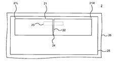
- FIG. 6 is a configuration diagram of an antenna according to another embodiment of the present invention.
- the antenna 2 has substantially the same configuration as the antenna 1 of the first embodiment. Therefore, the overlapping points are not described, and the differences from the first embodiment are described in detail.
- the antenna 2 includes a first antenna part 21, a conduction part 22, a second antenna part 23, a feeding point 24, a ground 25 and a dielectric substrate 26.
- the first antenna portion 21 does not have an antenna folded portion.
- the width of the first antenna portion 21 is longer than the width of the first antenna portion 11 of the first embodiment because there is no antenna turn-back portion.
- the second antenna portion 23 has a rectangular shape in this example.
- the width of the second antenna portion 23 is longer than the width w2 of the second antenna portion 13 of the first embodiment. Since the first antenna portion 21 does not have an antenna folded portion, the width of the second antenna portion 23 can be longer than the width w2 of the second antenna portion 13 of the first embodiment.
- the shape of the second antenna portion 23 is not limited to a rectangular shape, and may be T-shaped like the second antenna portion 13 of the first embodiment, and may have two desired frequencies. Any shape is possible as long as it can resonate.
- This embodiment also has the same effect as the first embodiment.
- the width of the second antenna portion 23 is longer than the width w2 of the second antenna portion 13 of the first embodiment. It is possible to take. Accordingly, there is an effect that the shape of the second antenna portion 23 can be determined more flexibly.
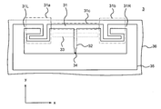
- FIG. 7 is a configuration diagram of an antenna according to another embodiment of the present invention.
- the antenna 3 has substantially the same configuration as the antenna 1 of the first embodiment. Therefore, the overlapping points are not described, and the differences from the first embodiment are described in detail.
- the antenna 3 includes a first antenna part 31, a conduction part 32, a second antenna part 33, a feeding point 34, a ground 35, and a dielectric substrate 36.
- the antenna folding method is different.
- the straight line part 31c of the 1st antenna part 31 is connected to the antenna folding
- a direction horizontal to the straight line portion 31c of the first antenna unit 31 is defined as an x direction, and a vertical direction is defined as a y direction.
- the first antenna portion 31 is folded so that the horizontal portion of the first antenna portion 31 and the horizontal portion 31c become longer.
- the antenna folded portions 31a and 31b are formed to be longer in the x direction and shorter in the y direction.
- the method of folding the antenna is not limited to these, and any folding method may be used as long as a desired frequency can be transmitted and received.
- This embodiment also has the same effect as the second embodiment.
- FIG. 8 is a configuration diagram of an antenna according to another embodiment of the present invention.
- the antenna 4 has substantially the same configuration as the antenna 1 of the first embodiment.
- the shape of the 1st antenna part 41 and the 2nd antenna part 43 differs from 1st Embodiment. Therefore, the overlapping points are not described, and the differences from the first embodiment are described in detail.
- the antenna 4 includes a first antenna part 41, a conduction part 42, a second antenna part 43, a feeding point 44, a ground 45 and a dielectric substrate 46.
- the shape of the first antenna unit 41 is a polygonal shape.
- the shape of the 2nd antenna part 43 is a rhombus.
- the shape of the second antenna unit 43 is not limited to this, and may be a polygonal shape such as a hexagon.
- FIG. 9 is a configuration diagram of an antenna according to another embodiment of the present invention.
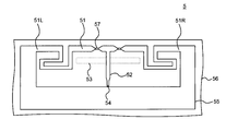
- the antenna 5 has substantially the same configuration as the antenna 3 of the third embodiment. Therefore, the overlapping points are not described, and the differences from the third embodiment are described in detail.
- the antenna 5 includes a first antenna part 51, a conduction part 52, a second antenna part 53, a feeding point 54, a ground 55, a dielectric substrate 56 and a chip capacitor 57.
- a chip capacitor 57 may be inserted into the first antenna unit 51. Thereby, it can replace with the electrostatic capacitance which the 1st antenna part 11 of a 1st embodiment has.
- This embodiment also has the same effects as those of the second to fourth embodiments.
- FIG. 10A is a configuration diagram of an antenna according to another embodiment of the present invention.
- FIG. 10B is a diagram for explaining a simulation state for confirming the VSWR frequency characteristic of the antenna according to another embodiment of the present invention.
- the antenna 6 has substantially the same configuration as the antenna 1 of the first embodiment. Unlike the first embodiment, the present embodiment is an antenna that resonates at three frequencies. Therefore, the overlapping points are not described, and the differences from the first embodiment are described in detail.
- the antenna 6 includes a first antenna portion 61, a conduction portion 62, a feeding point 64, a ground 65, and a derivative substrate 66.
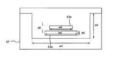
- the antenna 6 includes two second antenna portions 63a arranged in a region defined by a relationship between the first antenna portion 61, the conducting portion 62, and a region where both ends of the first antenna portion 61 are short-circuited and grounded. And 63b.
- the second antenna unit 63 a and the second antenna unit 63 b are arranged in a region formed by the ground 65 and the first antenna unit 61.
- the simulation conditions for confirming the VSWR frequency characteristics of the antenna 6 are as follows. That is, the antenna substrate layer is formed of three layers as in the first embodiment. In the present embodiment, unlike the first embodiment, the second antenna unit 63a and the second antenna unit 63b are arranged on the third substrate layer L3.
- d4 14 mm
- w1 51 mm
- d5 3 mm
- w5 36 mm
- d6 4 mm
- w6 24 mm.
- the distance between the plane on which the second antenna parts 63a and 63b are formed and the plane on which the conducting part 62 is formed is 1.6 mm.
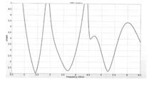
- FIG. 11 is a simulation result showing the VSWR frequency characteristics of an antenna according to an embodiment of the present invention.
- the value of VSWR is close to 1, and it can be seen that the efficiency with which the antenna radiates electric energy is the best around 2.4 GHz, 3.7 GHz, and 5.25 GHz. That is, the characteristic impedance is adjusted at three resonance frequencies near 2.4 GHz, 3.7 GHz, and 5.25 GHz.
- the number of second antenna units is not limited to two.
- (N ⁇ 1) second antenna units may be provided so as to resonate with the first antenna unit 61 at n frequencies.
- the (n ⁇ 1) second antenna units are arranged in a region determined in relation to the first antenna unit 61, the conduction unit 62, and a region where both ends of the first antenna unit 61 are short-circuited and grounded.
- This embodiment also has the same effect as the first embodiment.
- electrical_connection part demonstrated on the premise that the edge part connected with a feeding point was made thin.
- the antenna 7 shown in FIG. 12 is different from the antenna 1 according to the first embodiment in the conduction part. That is, unlike the conducting portion 12, the conducting portion 72 does not have a narrow end.
- the description has been made on the assumption that the antenna has three substrate layers.
- the antenna has three substrate layers. It is not limited to, and a plurality of layers other than three layers may be used.
- the first antenna unit 11 and the ground 15 are arranged on the first substrate layer L1 of the antenna substrate layer.
- the first antenna portion may be disposed on the first substrate layer, and the ground may be disposed on the second substrate layer. In this case, the same effects as those of the first embodiment can be obtained by providing through holes in the first substrate layer so that both ends of the first antenna unit and the ground are electrically connected.
- the substrate layer of the antenna is a plurality of layers of three or more layers, there is an effect that the degree of freedom in designing the wiring and the like is increased.
- the above antenna can be used in wireless LAN access points, etc., and can also be installed in multiband applications.
- the conductive portion may be connected to the first antenna portion at a midpoint between both ends of the first antenna portion.
- the first antenna part and the conduction part may be formed in the same layer.
- a capacitor may be inserted into the first antenna unit.
- the second antenna portion 13 is T-shaped.
- the T-shape is not limited to a combination of two rectangles, and may be a combination of two ellipses.
- the shape of each side of the rectangle forming the T-shape may be slightly warped.
- the number of the second antenna units is two.
- the number of the second antenna units is appropriately changed according to the frequency to be resonated. May be designed.
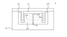
- three second antenna units 83a to 83c may be provided so as to resonate with the first antenna unit 81 at four frequencies.
- the width of the second antenna portion 83c is longer than the width of the second antenna portion 83b.
- the width of the second antenna part 83b is longer than the width of the second antenna part 83a.
- the second antenna parts 83a to 83c are arranged in a region defined in relation to a region where the first antenna unit 81, the conduction unit 82, and both ends of the first antenna unit 81 are short-circuited and grounded.
- the second antenna unit 83a, the second antenna unit 83b, and the second antenna unit 83c, which are short from the first antenna unit 81 side, are arranged in this order, but the arrangement order is limited to this. It is not a thing.
- the second antenna unit 83c having the longest width may be disposed on the first antenna unit 81 side, and the second antenna unit 83c may be disposed in the middle of the three second antenna units. .
- antennas 11, 21, 31, 41, 51, 61, 71 first antenna portion 11L, 21L, 31L, 41L, 51L, 61L, 71L: first antenna Left end portions 11R, 21R, 31R, 41R, 51R, 61R, 71R: right end portions 12, 22, 32, 42, 52, 62, 72 of the first antenna portion: conductive portions 13, 23, 33, 43, 53 63a, 63b, 73: second antenna portion 14, 24, 34, 44, 54, 64, 74: feeding points 15, 17, 25, 35, 45, 55, 65, 67: ground 16, 26, 36, 46, 56, 76: Dielectric substrate 47: Chip capacitor
Landscapes
- Details Of Aerials (AREA)
- Waveguide Aerials (AREA)
Abstract
より薄型のマルチバンドアンテナを提供する。本発明の一実施形態によれば、線状の第1アンテナ部と、前記第1アンテナ部と給電点とを接続する導通部と、前記第1アンテナ部の両端を短絡して接地する領域と、前記導通部と誘電体を挟んで少なくとも一部が導通部と重畳し、前記領域と前記第1アンテナ部とで囲まれた領域に配置される第2アンテナ部とを備えるアンテナが提供される。前記導通部は、前記第1アンテナ部の両端の間の中点で、前記第1アンテナ部と接続してもよい。
Description
本発明は、アンテナに関する。本発明は、特に、複数の周波帯域で共振する、良好な特性の薄型アンテナに関する。
従来、2つの周波数に対応した、いわゆるデュアルバンドアンテナを提供するために、グラウンド(GND)上に配置された放射導体と当該放射導体に近接して配置される無給電のグラウンドに短絡された素子とを備える技術が開示されている(例えば、特許文献1)。
しかしながら、グラウンド上に配置された放射導体と当該放射導体に近接して配置される無給電のグラウンドに短絡された素子で構成されており、特性インピーダンスを調整するため、相応の距離が必要となり、低背化(薄型化)には限界がある。
本発明は、上記のような従来技術に伴う課題を解決しようとするものであって、その目的とするところは、より薄型のマルチバンドアンテナを提供するところにある。
本発明の一実施形態によると、線状の第1アンテナ部と、前記第1アンテナ部と給電点とを接続する導通部と、前記第1アンテナ部の両端を短絡して接地する領域と、前記導通部と誘電体を挟んで少なくとも一部が導通部と重畳し、前記領域と前記第1アンテナ部とで囲まれた領域に配置される第2アンテナ部とを備えるアンテナが提供される。
本発明の一実施形態によると、線状の第1アンテナ部と、前記第1アンテナ部と給電点とを接続する導通部と、前記第1アンテナ部の両端を短絡して接地する領域と、前記第1アンテナ部とn個(nは2以上)の周波数で共振するように前記第1アンテナ部、前記導通部及び前記領域との関係で定められた領域に配置される(n-1)個の第2アンテナ部と、を備えるアンテナが提供される。
本発明によれば、より薄型のマルチバンドアンテナを提供することができる。
以下、本発明の一実施形態について、図面を参照しながら詳細に説明する。以下に示す実施形態は本発明の実施形態の一例であって、本発明はこれらの実施形態に限定されるものではない。なお、本実施形態で参照する図面において、同一部分または同様な機能を有する部分には同一の符号または類似の符号(数字の後にA、Bなどを付しただけの符号)を付し、その繰り返しの説明は省略する場合がある。また、図面の寸法比率は説明の都合上実際の比率とは異なったり、構成の一部が図面から省略されたりする場合がある。
<第1実施形態>
図1及び図2を用いて、本発明の一実施形態に係るアンテナについて説明する。図1は、本発明の一実施形態に係るアンテナの構成図である。図2は、本発明の一実施形態に係るアンテナの基板層構成を示す図である。アンテナ1は、第1アンテナ部11、導通部12、第2アンテナ部13、給電点14、グラウンド15、誘導体基板16を含む。この例では、アンテナの基板層は、3層であり、第1基板層L1、第2基板層L2及び第3基板層L3を含む。
図1及び図2を用いて、本発明の一実施形態に係るアンテナについて説明する。図1は、本発明の一実施形態に係るアンテナの構成図である。図2は、本発明の一実施形態に係るアンテナの基板層構成を示す図である。アンテナ1は、第1アンテナ部11、導通部12、第2アンテナ部13、給電点14、グラウンド15、誘導体基板16を含む。この例では、アンテナの基板層は、3層であり、第1基板層L1、第2基板層L2及び第3基板層L3を含む。
第1アンテナ部11は、この例では、誘電体基板16上にプリントすることによって作成された平面アンテナである。
第1アンテナ部11の形状は、線状である。ここで、線状とは、線のように細長く幅がないものではなく、幅を有するものである。幅は、図6に示すように第1アンテナ部61のすべてにおいて一定の幅であってもよいし、図8に示すように場所ごとに異なる幅であってもよい。記号11Lは、第1アンテナ部11の左端部を意味し、記号11Rは、第1アンテナ部11の右端部を意味する。左端部と右端部を合わせて、両端部と呼ぶ。この例では、第1基板層L1に第1アンテナ部11が配置される。また、この例では、第1アンテナ部11は、アンテナ折り返し部11a及び11bを有する。また、第1アンテナ部11の直線部11cは、アンテナ折り返し部11a及び11bに接続する。ここで、第1アンテナ部11の直線部11cと水平な方向をx方向とし、垂直な方向をy方向とする。アンテナ折り返し部11a及び11bは、y方向に長く、x方向に短くなるように形成される。その結果、第1アンテナ部11をx方向に短く形成することができる。
また、第1アンテナ部11の左端部11Lから右端部11Rまでの長さが共振周波数と相関関係を有する。そのため、アンテナ折り返し部を有する場合には、アンテナ折り返し部を有しない場合よりも、アンテナをより小型化することができる。
導通部12は、第1アンテナ部11と給電点14とを接続する。この例では、導通部12は、第1アンテナ部11の両端の間の中点で、第1アンテナ部11と接続する。導通部12の位置は、第1アンテナ部11の両端の間の中点で、第1アンテナ部11と接続する位置に限定されるものではない。また、この例では、導通部12は、第1アンテナ部11と同一の層に形成される。ここで、第2アンテナ部13は、無給電素子であるが、無給電素子による新たな共振点を発生させるためには、導通部12の影響を受ける位置に配置する必要がある。そこで、導通部12は、誘電体を挟んで少なくとも一部が第2アンテナ部13と重畳する位置であってもよい。ただし、導通部12を第1アンテナ部11の両端の間の中点からずらした位置で第1アンテナ部11と接続させると、放射パターンが無指向性を示さないものとなる。本実施形態では、導通部12は、第1アンテナ部11の両端の間の中点で、第1アンテナ部11と接続している。また、この例では、導通部12は、アンテナの特性インピーダンスを微調整するため、給電点14と接続する端部を細くしている。
グラウンド15は、第1アンテナ部11の両端を短絡して接地する領域に形成される。第1アンテナ部11がグラウンド15に接続しており、ループ状に動作する。なお、第1アンテナ部11の両端部がグラウンド15の左右に接続されているため、電流分布は、グラウンド15全体へ広がるのではなく、第1アンテナ部11に近い領域に集中する分布となる。
第2アンテナ部13は、導通部12と第2基板層L2として配置される誘電体(図示せず)を挟んで少なくとも一部が導通部12と重畳するように配置される。また、第2アンテナ部13は、グラウンド15と第1アンテナ部11とで形成する領域に配置される。すなわち、第2アンテナ部13は、誘電体を挟んで、第1アンテナ部11及びグラウンド15とは重畳しない。第2アンテナ部13は、第1アンテナ部11と複数の周波数で共振するように第1アンテナ部11、導通部12及びグラウンド15と第1アンテナ部11とで形成する領域との関係で定められた領域に配置される。また、この例では、第3基板層L3に、第2アンテナ部13が配置される。
第2アンテナ部13は、第1アンテナ部11と異なり、給電点に接続されておらず、無給電のアンテナ素子である。第2アンテナ部13から電波を送信するためには、導通部12から影響を受けて、第2アンテナ部13に高周波電流が流れる必要がある。そのため、第2アンテナ部13は、導通部12からある程度の距離の位置に配置されなければならない。他方、第2アンテナ部13を導通部12に近づけすぎると、VSWR(Voltage Standing Wave Ratio:電圧定在波比)の周波数特性が悪化する。
第2アンテナ部13が形成される平面と導通部12が形成される平面との距離の範囲を求めるために、図3A及び図3Bに示すアンテナの形状で、第2アンテナ部13が形成される平面と導通部12が形成される平面との距離を動かした。この距離を動かしたときに、図4に示すように2.5GHz付近及び5GHz付近で、特性インピーダンスの調整が取れているかどうかを確認し、この調整が取れている範囲を求めた。
図3A及び図3Bに示すアンテナの形状で、w1=35mm、d1=14mm、w2=16mm、d2=6.5mm、d3=3mmの条件で、第2アンテナ部13が形成される平面と導通部12が形成される平面との距離が第1アンテナの共振周波数に対してλ/250のときに、アンテナのVSWR周波数特性を確認するためのシミュレーションを行った。その結果、図4に示すようなシミュレーション結果を得て、2.5GHz付近及び5GHz付近で、特性インピーダンスの調整が取れていることを確認した。
他方、図3A及び図3Bに示すアンテナの形状で、w1=35mm、d1=14mm、w2=14mm、d2=6.5mm、d3=4mmの条件で、第2アンテナ部13が形成される平面と導通部12が形成される平面との距離が第1アンテナの共振周波数に対してλ/25のときに、アンテナのVSWR周波数特性を確認するためのシミュレーションを行った。その結果、図4に示すようなシミュレーション結果を得て、2.5GHz付近及び5GHz付近で、特性インピーダンスの調整が取れていることを確認した。
そこで、好ましくは、第2アンテナ部13が形成される平面と導通部12が形成される平面との距離は、第1アンテナの共振周波数に対して、λ/250以上λ/25以下である。
第2アンテナ部13は、この例では、インピーダンスの最適化のため、T字形状である。もっとも、第2アンテナ部13の形状は、これに限定されるものではなく、第1アンテナ部11と合わせて、2つの所望の周波数を送受信することが可能であれば長方形等の形状であってもよい。
図2に示すように、アンテナの基板層は、3層であり、第1基板層L1、第2基板層L2及び第3基板層L3を含む。第1基板層L1は、第1アンテナ部11及びグラウンド15を含む。第2基板層L2は、誘電体を含む。この例では、第2基板層L2の誘電体の材料は、ガラスエポキシFR4で、比誘電率εr=4.7で、厚さは、0.6mmである。もっとも、第2基板層L2の誘電体の材料は、ガラスエポキシFR4に限定されるものではなく、テフロン(登録商標)基板等であってもよい。また、第2基板層L2の誘電体は、空気であってもよい。空気の場合には、第1基板層L1とダイ3基板層L3との間は、空間となる。なお、比誘電率が大きいと、波長は短縮され、第2基板層L2の厚さも薄くなる。そして、空気よりもガラスエポキシFR4の方が比誘電率は大きい。そのため、誘電体が空気の場合よりもガラスエポキシFR4の方が、第2基板層L2の厚さが薄くなるという効果を奏する。
第3基板層L3は、第2アンテナ部13及びグラウンド(図示せず)を含む。この例では、グラウンドは、図3Bのグラウンド17に示すように、第1基板層L1のグラウンド15と同じ形状・大きさである。もっとも、グラウンド17はなくてもよい。
<シミュレーション条件>
図3A及び図3Bは、本発明の一実施形態に係るアンテナのVSWR周波数特性及び放射パターンを確認するためのシミュレーション状況を説明するための図である。
図3A及び図3Bは、本発明の一実施形態に係るアンテナのVSWR周波数特性及び放射パターンを確認するためのシミュレーション状況を説明するための図である。
このシミュレーションでは、アンテナの基板層は、3層で形成される。図3Aは、第1基板層L1側から見た図である。第1基板層L1には、第1アンテナ部11、導通部12、給電点14、グラウンド15が配置される。第2基板層L2には、誘電体が配置される。図3Bは、第3基板層L3側から見た図である。第3基板層L3には、第2アンテナ部13及びグラウンド17が配置される。
図3A及び図3Bに示すように、第1アンテナ部11の両端部間の長さw1=35mmであり、グラウンド15の縦の長さd1=14mmである。また、第2アンテナ部13は、T字形状をしており、w2=17.5mm、d2=5mm、d3=4mmである。そして、アンテナの第2基板層L2の厚さは、0.6mmである。
第2基板層L2の誘電体は、ガラスエポキシFR4で、比誘電率εr=4.7で、厚さは、0.6mmである。
<シミュレーション結果>
図4は、本発明の一実施形態に係るアンテナのVSWR周波数特性を示すシミュレーション結果である。図5は、本発明の一実施形態に係るアンテナの放射パターンを確認するためのシミュレーション結果である。
図4は、本発明の一実施形態に係るアンテナのVSWR周波数特性を示すシミュレーション結果である。図5は、本発明の一実施形態に係るアンテナの放射パターンを確認するためのシミュレーション結果である。
図4の破線は、第1アンテナ部11はあるが、第2アンテナ部(第2の共振素子)13がない場合のVSWRを示し、図4の実線は、第1アンテナ部(第1の共振素子)11に加えて、第2アンテナ部(第2の共振素子)13がある場合のVSWRを示す。
図4の破線が示すように、第1アンテナ部11はあるが、第2アンテナ部13がない場合には、2.5GHz付近では、VSWRの値が1に近くなっているのに対し、5~6GHz付近では、VSWRの値が1から離れた値となっている。
他方、図4の実線が示すように、第1アンテナ部11に加えて、第2アンテナ部13がある場合には、2.5GHz付近及び5GHz付近で、VSWRの値が1に近くなっており、2.5GHz付近及び5GHz付近で、アンテナが電気エネルギーを放射する効率が最も良くなっていることがわかる。すなわち、2.5GHz付近及び5GHz付近で、特性インピーダンスの調整が取れていることになる。
図4の実線及び破線から、第2アンテナ部13の追加によって、5~6GHz帯で新たな共振点が発生していることがわかる。また、シミュレーションの対象となったアンテナは、アンテナの第2基板層L2の厚さが0.6mmであっても、2.5GHz付近と5GHz付近の2つの周波数帯域でアンテナとして機能するデュアルバンドアンテナであるといえる。
図5Aは、第1アンテナ部11による放射パターン(2.4GHz帯)を示す図である。図5Bは、第1アンテナ部11に第2アンテナ部13を加えたことで発生した共振点での放射パターン(5GHz帯)を示す図である。
図5AのH1(破線)が水平偏波の利得を示し、図5AのV1(実線)が垂直偏波の利得を示す。また、図5BのH2(破線)が水平偏波の利得を示し、図5BのV2(実線)が垂直偏波の利得を示す。なお、利得の値は、アイソトロピックアンテナを基準とする値(dBi)で示している。
図5AのH1及び図5BのH2が示すように、概ね無指向性の放射パターンとなり、最大利得は2dBi程度と良好な特性であることがわかる。
従来技術では、グラウンド上に配置された放射導体と当該放射導体に近接して配置される無給電のグラウンドに短絡された素子で構成されており、薄型化には限界がある。他方、本実施形態では、第1アンテナ部11は、グラウンド15と同一平面状に形成することができる。そのため、アンテナの基板層の第2基板層L2の厚さを薄くすることができる。具体的には、アンテナの基板層の第2基板層L2の厚さが、λ/200であっても、マルチバンドアンテナ(デュアルバンドアンテナ)として機能する。したがって、従来技術よりも、より薄型のマルチバンドアンテナ(デュアルバンドアンテナ)を提供することができるという効果を奏する。
また、従来技術では、放射導体と当該放射導体と同一水平面状に無給電のグラウンドに短絡された素子が配置されるため、放射パターンに偏りが生じるという問題がある。他方、本実施形態では、図5AのH1及び図5BのH2が示すように、放射パターンに偏りが生じないという効果を奏する。
さらに、従来技術では、グラウンドに短絡された素子を用いるため、グラウンド依存性が高く、設置するグラウンドの形状によって、特性が大きく変わるという問題がある。他方、本実施形態では、第1アンテナ部11がグラウンド15に接続しており、ループ状に動作する。そのため、グラウンド依存性が低く、良好な放射パターンが得られるという効果を奏する。
また、本実施形態では、第1アンテナ部11は、左右にアンテナ折り返し部を有する。この場合には、第1アンテナ部11の幅の長さを短くすることができ、省スペース化できるという効果を奏する。
<第2実施形態>
図6を用いて、本発明の他の実施形態に係るアンテナについて説明する。図6は、本発明の他の実施形態に係るアンテナの構成図である。アンテナ2は、第1実施形態のアンテナ1と概ね同じ構成である。そこで、重複する点についての説明はせず、第1実施形態と異なる点について、詳細な説明をする。
図6を用いて、本発明の他の実施形態に係るアンテナについて説明する。図6は、本発明の他の実施形態に係るアンテナの構成図である。アンテナ2は、第1実施形態のアンテナ1と概ね同じ構成である。そこで、重複する点についての説明はせず、第1実施形態と異なる点について、詳細な説明をする。
アンテナ2は、第1アンテナ部21、導通部22、第2アンテナ部23、給電点24、グランド25及び誘導体基板26を含む。本実施形態では、第1アンテナ部21には、アンテナ折り返し部はない。第1アンテナ部21の幅の長さは、アンテナ折り返し部がないため、第1実施形態の第1アンテナ部11の幅の長さより長い。
第2アンテナ部23は、この例では、長方形の形状である。第2アンテナ部23の幅の長さは、第1実施形態の第2アンテナ部13の幅の長さw2よりも長い。第1アンテナ部21にアンテナ折り返し部がないため、第2アンテナ部23の幅の長さが第1実施形態の第2アンテナ部13の幅の長さw2よりも長い構成をとることが可能となる。もっとも、第2アンテナ部23の形状は、長方形の形状に限定されるものではなく、第1実施形態の第2アンテナ部13のようにT字形状であってもよいし、所望の2つの周波数で共振することが可能であればいかなる形状でもよい。
本実施形態でも、第1実施形態と同様の効果を奏する。
本実施形態では、第1アンテナ部21にアンテナ折り返し部がないため、第2アンテナ部23の幅の長さが第1実施形態の第2アンテナ部13の幅の長さw2よりも長い構成をとることが可能となる。それに伴い、第2アンテナ部23の形状をより柔軟に決めることができるという効果を奏する。
<第3実施形態>
図7を用いて、本発明の他の実施形態に係るアンテナについて説明する。図7は、本発明の他の実施形態に係るアンテナの構成図である。アンテナ3は、第1実施形態のアンテナ1と概ね同じ構成である。そこで、重複する点についての説明はせず、第1実施形態と異なる点について、詳細な説明をする。
図7を用いて、本発明の他の実施形態に係るアンテナについて説明する。図7は、本発明の他の実施形態に係るアンテナの構成図である。アンテナ3は、第1実施形態のアンテナ1と概ね同じ構成である。そこで、重複する点についての説明はせず、第1実施形態と異なる点について、詳細な説明をする。
アンテナ3は、第1アンテナ部31、導通部32、第2アンテナ部33、給電点34、グランド35及び誘導体基板36を含む。本実施形態でも、第1アンテナ部31と同様に、アンテナ折り返し部31a及び31bがあるが、アンテナの折り返し方が異なる。また、第1アンテナ部31の直線部31cは、アンテナ折り返し部31a及び31bに接続する。ここで、第1アンテナ部31の直線部31cと水平な方向をx方向とし、垂直な方向をy方向とする。第1実施形態と比較すると、本実施形態では、第1アンテナ部31は、第1アンテナ部31の直線部31cと水平な部分が長くなるように折り返される。すなわち、第1実施形態と比較すると、アンテナ折り返し部31a及び31bは、x方向により長く、y方向により短くなるように形成される。もっとも、アンテナの折り返し方は、これらに限定されるものではなく、所望の周波数を送受信することが可能であればいかなる折り返し方であってもよい。
本実施形態でも、第2実施形態と同様の効果を奏する。
<第4実施形態>
図8を用いて、本発明の他の実施形態に係るアンテナについて説明する。図8は、本発明の他の実施形態に係るアンテナの構成図である。アンテナ4は、第1実施形態のアンテナ1と概ね同じ構成である。本実施形態では、第1実施形態とは、第1アンテナ部41及び第2アンテナ部43の形状が異なる。そこで、重複する点についての説明はせず、第1実施形態と異なる点について、詳細な説明をする。
図8を用いて、本発明の他の実施形態に係るアンテナについて説明する。図8は、本発明の他の実施形態に係るアンテナの構成図である。アンテナ4は、第1実施形態のアンテナ1と概ね同じ構成である。本実施形態では、第1実施形態とは、第1アンテナ部41及び第2アンテナ部43の形状が異なる。そこで、重複する点についての説明はせず、第1実施形態と異なる点について、詳細な説明をする。
アンテナ4は、第1アンテナ部41、導通部42、第2アンテナ部43、給電点44、グランド45及び誘導体基板46を含む。第1アンテナ部41の形状は、多角形状である。また、第2アンテナ部43の形状は、ひし形である。第2アンテナ部43の形状は、これに限定されるものではなく、六角形等の多角形状であってもよい。
本実施形態でも、第2実施形態及び第3実施形態と同様の効果を奏する。
<第5実施形態>
図9を用いて、本発明の他の実施形態に係るアンテナについて説明する。図9は、本発明の他の実施形態に係るアンテナの構成図である。アンテナ5は、第3実施形態のアンテナ3と概ね同じ構成である。そこで、重複する点についての説明はせず、第3実施形態と異なる点について、詳細な説明をする。
図9を用いて、本発明の他の実施形態に係るアンテナについて説明する。図9は、本発明の他の実施形態に係るアンテナの構成図である。アンテナ5は、第3実施形態のアンテナ3と概ね同じ構成である。そこで、重複する点についての説明はせず、第3実施形態と異なる点について、詳細な説明をする。
アンテナ5は、第1アンテナ部51、導通部52、第2アンテナ部53、給電点54、グランド55、誘導体基板56及びチップコンデンサ57を含む。
本実施形態では、第1アンテナ部51にチップコンデンサ57を挿入してもよい。これによって、第1実施形態の第1アンテナ部11が有する静電容量の代わりとすることができる。
本実施形態でも、第2実施形態乃至第4実施形態と同様の効果を奏する。
<第6実施形態>
第1実施形態乃至第5実施形態では、デュアルバンドアンテナを前提に説明した。図10A及び図10Bを用いて、本発明の他の実施形態に係るアンテナについて説明する。図10Aは、本発明の他の実施形態に係るアンテナの構成図である。図10Bは、本発明の他の実施形態に係るアンテナのVSWR周波数特性を確認するためのシミュレーション状況を説明するための図である。アンテナ6は、第1実施形態のアンテナ1と概ね同じ構成である。本実施形態では、第1実施形態と異なり、3つの周波数で共振するアンテナである。そこで、重複する点についての説明はせず、第1実施形態と異なる点について、詳細な説明をする。
第1実施形態乃至第5実施形態では、デュアルバンドアンテナを前提に説明した。図10A及び図10Bを用いて、本発明の他の実施形態に係るアンテナについて説明する。図10Aは、本発明の他の実施形態に係るアンテナの構成図である。図10Bは、本発明の他の実施形態に係るアンテナのVSWR周波数特性を確認するためのシミュレーション状況を説明するための図である。アンテナ6は、第1実施形態のアンテナ1と概ね同じ構成である。本実施形態では、第1実施形態と異なり、3つの周波数で共振するアンテナである。そこで、重複する点についての説明はせず、第1実施形態と異なる点について、詳細な説明をする。
アンテナ6は、第1アンテナ部61、導通部62、給電点64、グラウンド65、誘導体基板66を含む。また、アンテナ6は、第1アンテナ部61、導通部62及び第1アンテナ部61の両端を短絡して接地する領域との関係で定められた領域に配置される2個の第2アンテナ部63a及び63bを有する。言い換えると、第2アンテナ部63a及び第2アンテナ部63bは、グラウンド65と第1アンテナ部61とで形成する領域に配置される。
アンテナ6のVSWR周波数特性を確認するためのシミュレーションの条件は以下のとおりである。すなわち、アンテナの基板層は、第1実施形態と同様に3層で形成される。本実施形態では、第1実施形態と異なり、第3基板層L3に、第2アンテナ部63a、第2アンテナ部63bが配置される。
また、図10A及び図10Bにおいて、d4=14mm、w1=51mm、d5=3mm、w5=36mm、d6=4mm、w6=24mmである。第2アンテナ部63a及び63bが形成される平面と導通部62が形成される平面との距離は、1.6mmである。
上記のシミュレーションの条件でシミュレーションしたところ、図11に示す結果を得た。図11は、本発明の一実施形態に係るアンテナのVSWR周波数特性を示すシミュレーション結果である。
図11の実線が示すように、第1アンテナ部61に加えて、第2アンテナ部63a及び第2アンテナ部63bがある場合には、2.4GHz付近、3.7GHz及び5.25GHz付近で、VSWRの値が1に近くなっており、2.4GHz付近、3.7GHz及び5.25GHz付近で、アンテナが電気エネルギーを放射する効率が最も良くなっていることがわかる。すなわち、2.4GHz付近、3.7GHz及び5.25GHz付近の3つの共振周波数で、特性インピーダンスの調整が取れていることになる。
もっとも、第2アンテナ部の個数は、2個に限定されるものではない。第1アンテナ部61とn個の周波数で共振するように、(n-1)個の第2アンテナ部を設けてもよい。なお、(n-1)個の第2アンテナ部は、第1アンテナ部61、導通部62及び第1アンテナ部61の両端を短絡して接地する領域との関係で定められた領域に配置される。
本実施形態でも、第1実施形態と同様の効果を奏する。
<変形例1>
第1実施形態乃至第6実施形態では、導通部は、給電点と接続する端部を細くしていることを前提として説明した。もっとも、第1実施形態乃至第6実施形態のいずれの実施形態においても、導通部の端部を細くしなくてもよい。例えば、図12に示すアンテナ7は、第1実施形態に係るアンテナ1と導通部が異なる。すなわち、導通部72は、導通部12と異なり、端部が細くなっていない。
第1実施形態乃至第6実施形態では、導通部は、給電点と接続する端部を細くしていることを前提として説明した。もっとも、第1実施形態乃至第6実施形態のいずれの実施形態においても、導通部の端部を細くしなくてもよい。例えば、図12に示すアンテナ7は、第1実施形態に係るアンテナ1と導通部が異なる。すなわち、導通部72は、導通部12と異なり、端部が細くなっていない。
本変形例においても、第1実施形態と同様の効果を奏する。
<変形例2>
第1実施形態乃至第6実施形態、変形例1では、アンテナの基板層が3層であることを前提に説明したが、いずれの実施形態、変形例1においても、アンテナの基板層は3層に限定されるものではなく、3層以外の複数の層であってもよい。例えば、第1実施形態では、アンテナの基板層の第1基板層L1に、第1アンテナ部11及びグラウンド15を配置されているが、アンテナの基板層が3層以上の層である場合には、第1基板層に、第1アンテナ部を配置し、第2基板層にグラウンドを配置してもよい。この場合には、第1基板層にスルーホールを設け、第1アンテナ部の両端とグラウンドが電気的に接続されるようにすれば、第1実施形態と同様の効果を得ることができる。
第1実施形態乃至第6実施形態、変形例1では、アンテナの基板層が3層であることを前提に説明したが、いずれの実施形態、変形例1においても、アンテナの基板層は3層に限定されるものではなく、3層以外の複数の層であってもよい。例えば、第1実施形態では、アンテナの基板層の第1基板層L1に、第1アンテナ部11及びグラウンド15を配置されているが、アンテナの基板層が3層以上の層である場合には、第1基板層に、第1アンテナ部を配置し、第2基板層にグラウンドを配置してもよい。この場合には、第1基板層にスルーホールを設け、第1アンテナ部の両端とグラウンドが電気的に接続されるようにすれば、第1実施形態と同様の効果を得ることができる。
第1実施形態乃至第6実施形態、変形例1に係るアンテナについて、アンテナの基板層を3層以上の複数の層にした場合には、配線等の設計の自由度が増すという効果を奏する。
上記のアンテナは、無線LANのアクセスポイントなどで応用されるほか、マルチバンドを用いる応用製品に搭載可能である。
前記導通部は、前記第1アンテナ部の両端の間の中点で、前記第1アンテナ部と接続してもよい。
前記第1アンテナ部と前記導通部とは、同一の層に形成されてもよい。
前記第1アンテナ部にコンデンサが挿入されてもよい。
前述のとおり、第2アンテナ部13は、T字形状である。T字形状は、長方形を2つ組み合わせた形状に限らず、楕円形を2つ組み合わせた形状であってもよい。T字を形成する長方形の各辺が多少反った形状であってもよい。
また、前述の第6実施形態において、第2アンテナ部の個数が複数の場合について説明した。すなわち、図10A、図10B及び図11に示す例では、第2アンテナ部の個数が2個であるが、前述のとおり、第2アンテナ部の個数は、共振させる周波数に応じて、適宜変更して設計してもよい。例えば、図13に示すように、第1アンテナ部81と4個の周波数で共振するように、3個の第2アンテナ部83aから83cを設けてもよい。第2アンテナ部83cの幅は、第2アンテナ部83bの幅よりも長い。同様に、第2アンテナ部83bの幅は、第2アンテナ部83aの幅よりも長い。第2アンテナ部83aから83cは、第1アンテナ部81、導通部82及び第1アンテナ部81の両端を短絡して接地する領域との関係で定められた領域に配置される。この例では、第1アンテナ部81側から幅が短い第2アンテナ部83a、第2アンテナ部83b、第2アンテナ部83cの順で配置されているが、配置の順は、これに限定されるものではない。例えば、第1アンテナ部81側に幅が一番長い第2アンテナ部83cが配置されてもよいし、第2アンテナ部83cは、3個の第2アンテナ部のうち真ん中に配置されてもよい。
なお、本発明は上記の実施形態に限られたものではなく、趣旨を逸脱しない範囲で適宜変更することが可能である。
1、2、3、4、5、6、7:アンテナ
11、21、31、41、51、61、71:第1アンテナ部
11L、21L、31L、41L、51L、61L、71L:第1アンテナ部の左端部
11R、21R、31R、41R、51R、61R、71R:第1アンテナ部の右端部
12、22、32、42、52、62、72:導通部
13、23、33、43、53、63a、63b、73:第2アンテナ部
14、24、34、44、54、64、74:給電点
15、17、25、35、45、55、65、67:グラウンド
16、26、36、46、56、76:誘電体基板
47:チップコンデンサ
11、21、31、41、51、61、71:第1アンテナ部
11L、21L、31L、41L、51L、61L、71L:第1アンテナ部の左端部
11R、21R、31R、41R、51R、61R、71R:第1アンテナ部の右端部
12、22、32、42、52、62、72:導通部
13、23、33、43、53、63a、63b、73:第2アンテナ部
14、24、34、44、54、64、74:給電点
15、17、25、35、45、55、65、67:グラウンド
16、26、36、46、56、76:誘電体基板
47:チップコンデンサ
Claims (7)
- 線状の第1アンテナ部と、
前記第1アンテナ部と給電点とを接続する導通部と、
前記第1アンテナ部の両端を短絡して接地する領域と、
前記導通部と誘電体を挟んで少なくとも一部が前記導通部と重畳し、前記領域と前記第1アンテナ部とで囲まれた領域に配置される第2アンテナ部と
を備えるアンテナ。 - 線状の第1アンテナ部と、
前記第1アンテナ部と給電点とを接続する導通部と、
前記第1アンテナ部の両端を短絡して接地する領域と、
前記第1アンテナ部とn個(nは2以上)の周波数で共振するように前記第1アンテナ部、前記導通部及び前記領域との関係で定められた領域に配置される(n-1)個の第2アンテナ部と、
を備えるアンテナ。 - 前記導通部は、前記第1アンテナ部の両端の間の中点で、前記第1アンテナ部と接続することを特徴とする請求項1又は請求項2に記載のアンテナ。
- 前記第1アンテナ部と前記導通部とは、同一の層に形成されることを特徴とする請求項1又は請求項2に記載のアンテナ。
- 前記第1アンテナ部にコンデンサが挿入されることを特徴とする請求項1乃至請求項4の何れか一に記載のアンテナ。
- 前記第2アンテナ部は、T字形状であることを特徴とする請求項1又は請求項2に記載のアンテナ。
- 前記導通部が形成される面と前記第2アンテナ部が形成される面との距離は、前記第1アンテナ部の共振周波数に対してλ/250以上λ/25以下であることを特徴とする請求項1又は請求項2に記載のアンテナ。
Priority Applications (2)
| Application Number | Priority Date | Filing Date | Title |
|---|---|---|---|
| CN201780017452.2A CN109155462B (zh) | 2016-03-22 | 2017-03-16 | 天线 |
| US16/135,518 US10916848B2 (en) | 2016-03-22 | 2018-09-19 | Antenna |
Applications Claiming Priority (2)
| Application Number | Priority Date | Filing Date | Title |
|---|---|---|---|
| JP2016-057137 | 2016-03-22 | ||
| JP2016057137A JP6607107B2 (ja) | 2016-03-22 | 2016-03-22 | アンテナ |
Related Child Applications (1)
| Application Number | Title | Priority Date | Filing Date |
|---|---|---|---|
| US16/135,518 Continuation US10916848B2 (en) | 2016-03-22 | 2018-09-19 | Antenna |
Publications (1)
| Publication Number | Publication Date |
|---|---|
| WO2017164059A1 true WO2017164059A1 (ja) | 2017-09-28 |
Family
ID=59900315
Family Applications (1)
| Application Number | Title | Priority Date | Filing Date |
|---|---|---|---|
| PCT/JP2017/010646 Ceased WO2017164059A1 (ja) | 2016-03-22 | 2017-03-16 | アンテナ |
Country Status (4)
| Country | Link |
|---|---|
| US (1) | US10916848B2 (ja) |
| JP (1) | JP6607107B2 (ja) |
| CN (1) | CN109155462B (ja) |
| WO (1) | WO2017164059A1 (ja) |
Families Citing this family (3)
| Publication number | Priority date | Publication date | Assignee | Title |
|---|---|---|---|---|
| KR102239022B1 (ko) * | 2019-09-16 | 2021-04-14 | 주식회사 갤트로닉스 코리아 | 폴더블 디바이스의 안테나 |
| JP7388743B2 (ja) * | 2021-06-18 | 2023-11-29 | Necプラットフォームズ株式会社 | アンテナ装置及び無線機器 |
| JP2023130159A (ja) * | 2022-03-07 | 2023-09-20 | Necプラットフォームズ株式会社 | 指向性アンテナ装置 |
Citations (4)
| Publication number | Priority date | Publication date | Assignee | Title |
|---|---|---|---|---|
| JP2005203878A (ja) * | 2004-01-13 | 2005-07-28 | Toshiba Corp | アンテナ装置及び携帯無線通信装置 |
| WO2013077302A1 (ja) * | 2011-11-25 | 2013-05-30 | 株式会社村田製作所 | アンテナ装置および電子機器 |
| JP2014017806A (ja) * | 2012-06-14 | 2014-01-30 | Yamaha Corp | アンテナ |
| JP2014042142A (ja) * | 2012-08-22 | 2014-03-06 | Yamaha Corp | アンテナユニット |
Family Cites Families (12)
| Publication number | Priority date | Publication date | Assignee | Title |
|---|---|---|---|---|
| JP2004201278A (ja) * | 2002-12-06 | 2004-07-15 | Sharp Corp | パターンアンテナ |
| US6977616B2 (en) | 2003-09-01 | 2005-12-20 | Alps Electric Co., Ltd. | Dual-band antenna having small size and low-height |
| JP4063741B2 (ja) | 2003-09-01 | 2008-03-19 | アルプス電気株式会社 | デュアルバンドアンテナ |
| US7079079B2 (en) * | 2004-06-30 | 2006-07-18 | Skycross, Inc. | Low profile compact multi-band meanderline loaded antenna |
| CN101154767B (zh) * | 2006-09-28 | 2011-08-31 | 香港城市大学 | 宽带天线 |
| ES2589144T3 (es) * | 2007-10-08 | 2016-11-10 | Tyco Fire & Security Gmbh | Antena de parche de RFID con tierra de referencia coplanar y tierras flotantes |
| JP5414996B2 (ja) * | 2008-01-21 | 2014-02-12 | 株式会社フジクラ | アンテナ及び無線通信装置 |
| CN201508908U (zh) * | 2009-07-22 | 2010-06-16 | 比亚迪股份有限公司 | 多频天线 |
| EP2461422A4 (en) * | 2009-07-27 | 2015-10-28 | Sharp Kk | ANTENNA DEVICE AND WIRELESS COMMUNICATION TERMINAL |
| CN102780071B (zh) * | 2011-05-10 | 2014-12-10 | 鸿富锦精密工业(深圳)有限公司 | 立体天线 |
| CN102394352B (zh) * | 2011-07-14 | 2014-01-08 | 东南大学 | 双频宽带可重构微带天线 |
| KR101360561B1 (ko) * | 2012-06-28 | 2014-02-11 | 엘지이노텍 주식회사 | 안테나 장치 |
-
2016
- 2016-03-22 JP JP2016057137A patent/JP6607107B2/ja active Active
-
2017
- 2017-03-16 CN CN201780017452.2A patent/CN109155462B/zh active Active
- 2017-03-16 WO PCT/JP2017/010646 patent/WO2017164059A1/ja not_active Ceased
-
2018
- 2018-09-19 US US16/135,518 patent/US10916848B2/en active Active
Patent Citations (4)
| Publication number | Priority date | Publication date | Assignee | Title |
|---|---|---|---|---|
| JP2005203878A (ja) * | 2004-01-13 | 2005-07-28 | Toshiba Corp | アンテナ装置及び携帯無線通信装置 |
| WO2013077302A1 (ja) * | 2011-11-25 | 2013-05-30 | 株式会社村田製作所 | アンテナ装置および電子機器 |
| JP2014017806A (ja) * | 2012-06-14 | 2014-01-30 | Yamaha Corp | アンテナ |
| JP2014042142A (ja) * | 2012-08-22 | 2014-03-06 | Yamaha Corp | アンテナユニット |
Also Published As
| Publication number | Publication date |
|---|---|
| CN109155462B (zh) | 2021-05-11 |
| US20190044233A1 (en) | 2019-02-07 |
| CN109155462A (zh) | 2019-01-04 |
| JP6607107B2 (ja) | 2019-11-20 |
| US10916848B2 (en) | 2021-02-09 |
| JP2017175275A (ja) | 2017-09-28 |
Similar Documents
| Publication | Publication Date | Title |
|---|---|---|
| US10008783B2 (en) | Patch antenna | |
| US20150303576A1 (en) | Miniaturized Patch Antenna | |
| EP3168927B1 (en) | Ultra compact ultra broad band dual polarized base station antenna | |
| US9252490B2 (en) | Multi-band antenna and electronic device provided with the same | |
| JP6500859B2 (ja) | 無線モジュール | |
| US7834809B2 (en) | Multi-antenna integration module | |
| US9431711B2 (en) | Broadband multi-strip patch antenna | |
| US10886620B2 (en) | Antenna | |
| JP6528496B2 (ja) | アンテナ装置 | |
| JP2007221774A (ja) | 平面型アンテナ | |
| JP2009135797A (ja) | アンテナ装置 | |
| US8441399B2 (en) | Three-dimensional slot antenna | |
| JP5542902B2 (ja) | アンテナ | |
| EP1085595B1 (en) | Surface-mounted antenna and communication apparatus using same | |
| WO2017178037A1 (en) | Antenna and radiating element for antenna | |
| KR101862060B1 (ko) | 다중대역에서 동작하는 소형 유사 등방성 안테나 | |
| US9306277B2 (en) | Multi-antenna device and communication device | |
| KR102463269B1 (ko) | 안테나 장치 및 단말기 | |
| JP6607107B2 (ja) | アンテナ | |
| US20130187726A1 (en) | Tunable variable impedance transmission line | |
| JP6393048B2 (ja) | マルチバンドアンテナ | |
| US8421681B2 (en) | Multi-band antenna | |
| JP2009124582A (ja) | アンテナ | |
| CN106159420B (zh) | 一种天线结构及无线装置 | |
| JP6201651B2 (ja) | アンテナ装置およびアレイアンテナ装置 |
Legal Events
| Date | Code | Title | Description |
|---|---|---|---|
| NENP | Non-entry into the national phase |
Ref country code: DE |
|
| 121 | Ep: the epo has been informed by wipo that ep was designated in this application |
Ref document number: 17770102 Country of ref document: EP Kind code of ref document: A1 |
|
| 122 | Ep: pct application non-entry in european phase |
Ref document number: 17770102 Country of ref document: EP Kind code of ref document: A1 |