WO2017163830A1 - Method for manufacturing electrically conductive laminate, and solid structure with layer to be plated precursor layer, solid structure with patterned layer to be plated, electrically conductive laminate, touch sensor, heat-generating member, and solid structure - Google Patents
Method for manufacturing electrically conductive laminate, and solid structure with layer to be plated precursor layer, solid structure with patterned layer to be plated, electrically conductive laminate, touch sensor, heat-generating member, and solid structure Download PDFInfo
- Publication number
- WO2017163830A1 WO2017163830A1 PCT/JP2017/008648 JP2017008648W WO2017163830A1 WO 2017163830 A1 WO2017163830 A1 WO 2017163830A1 JP 2017008648 W JP2017008648 W JP 2017008648W WO 2017163830 A1 WO2017163830 A1 WO 2017163830A1
- Authority
- WO
- WIPO (PCT)
- Prior art keywords
- layer
- plated
- pattern
- precursor
- group
- Prior art date
Links
Images


Classifications
-
- H—ELECTRICITY
- H05—ELECTRIC TECHNIQUES NOT OTHERWISE PROVIDED FOR
- H05K—PRINTED CIRCUITS; CASINGS OR CONSTRUCTIONAL DETAILS OF ELECTRIC APPARATUS; MANUFACTURE OF ASSEMBLAGES OF ELECTRICAL COMPONENTS
- H05K3/00—Apparatus or processes for manufacturing printed circuits
- H05K3/10—Apparatus or processes for manufacturing printed circuits in which conductive material is applied to the insulating support in such a manner as to form the desired conductive pattern
- H05K3/18—Apparatus or processes for manufacturing printed circuits in which conductive material is applied to the insulating support in such a manner as to form the desired conductive pattern using precipitation techniques to apply the conductive material
-
- B—PERFORMING OPERATIONS; TRANSPORTING
- B32—LAYERED PRODUCTS
- B32B—LAYERED PRODUCTS, i.e. PRODUCTS BUILT-UP OF STRATA OF FLAT OR NON-FLAT, e.g. CELLULAR OR HONEYCOMB, FORM
- B32B9/00—Layered products comprising a layer of a particular substance not covered by groups B32B11/00 - B32B29/00
- B32B9/04—Layered products comprising a layer of a particular substance not covered by groups B32B11/00 - B32B29/00 comprising such particular substance as the main or only constituent of a layer, which is next to another layer of the same or of a different material
- B32B9/045—Layered products comprising a layer of a particular substance not covered by groups B32B11/00 - B32B29/00 comprising such particular substance as the main or only constituent of a layer, which is next to another layer of the same or of a different material of synthetic resin
-
- B—PERFORMING OPERATIONS; TRANSPORTING
- B32—LAYERED PRODUCTS
- B32B—LAYERED PRODUCTS, i.e. PRODUCTS BUILT-UP OF STRATA OF FLAT OR NON-FLAT, e.g. CELLULAR OR HONEYCOMB, FORM
- B32B1/00—Layered products having a general shape other than plane
-
- B—PERFORMING OPERATIONS; TRANSPORTING
- B32—LAYERED PRODUCTS
- B32B—LAYERED PRODUCTS, i.e. PRODUCTS BUILT-UP OF STRATA OF FLAT OR NON-FLAT, e.g. CELLULAR OR HONEYCOMB, FORM
- B32B15/00—Layered products comprising a layer of metal
- B32B15/04—Layered products comprising a layer of metal comprising metal as the main or only constituent of a layer, which is next to another layer of the same or of a different material
-
- B—PERFORMING OPERATIONS; TRANSPORTING
- B32—LAYERED PRODUCTS
- B32B—LAYERED PRODUCTS, i.e. PRODUCTS BUILT-UP OF STRATA OF FLAT OR NON-FLAT, e.g. CELLULAR OR HONEYCOMB, FORM
- B32B23/00—Layered products comprising a layer of cellulosic plastic substances, i.e. substances obtained by chemical modification of cellulose, e.g. cellulose ethers, cellulose esters, viscose
- B32B23/04—Layered products comprising a layer of cellulosic plastic substances, i.e. substances obtained by chemical modification of cellulose, e.g. cellulose ethers, cellulose esters, viscose comprising such cellulosic plastic substance as the main or only constituent of a layer, which is next to another layer of the same or of a different material
- B32B23/08—Layered products comprising a layer of cellulosic plastic substances, i.e. substances obtained by chemical modification of cellulose, e.g. cellulose ethers, cellulose esters, viscose comprising such cellulosic plastic substance as the main or only constituent of a layer, which is next to another layer of the same or of a different material of synthetic resin
-
- B—PERFORMING OPERATIONS; TRANSPORTING
- B32—LAYERED PRODUCTS
- B32B—LAYERED PRODUCTS, i.e. PRODUCTS BUILT-UP OF STRATA OF FLAT OR NON-FLAT, e.g. CELLULAR OR HONEYCOMB, FORM
- B32B27/00—Layered products comprising a layer of synthetic resin
- B32B27/06—Layered products comprising a layer of synthetic resin as the main or only constituent of a layer, which is next to another layer of the same or of a different material
- B32B27/08—Layered products comprising a layer of synthetic resin as the main or only constituent of a layer, which is next to another layer of the same or of a different material of synthetic resin
-
- B—PERFORMING OPERATIONS; TRANSPORTING
- B32—LAYERED PRODUCTS
- B32B—LAYERED PRODUCTS, i.e. PRODUCTS BUILT-UP OF STRATA OF FLAT OR NON-FLAT, e.g. CELLULAR OR HONEYCOMB, FORM
- B32B27/00—Layered products comprising a layer of synthetic resin
- B32B27/18—Layered products comprising a layer of synthetic resin characterised by the use of special additives
-
- B—PERFORMING OPERATIONS; TRANSPORTING
- B32—LAYERED PRODUCTS
- B32B—LAYERED PRODUCTS, i.e. PRODUCTS BUILT-UP OF STRATA OF FLAT OR NON-FLAT, e.g. CELLULAR OR HONEYCOMB, FORM
- B32B27/00—Layered products comprising a layer of synthetic resin
- B32B27/28—Layered products comprising a layer of synthetic resin comprising synthetic resins not wholly covered by any one of the sub-groups B32B27/30 - B32B27/42
- B32B27/285—Layered products comprising a layer of synthetic resin comprising synthetic resins not wholly covered by any one of the sub-groups B32B27/30 - B32B27/42 comprising polyethers
-
- B—PERFORMING OPERATIONS; TRANSPORTING
- B32—LAYERED PRODUCTS
- B32B—LAYERED PRODUCTS, i.e. PRODUCTS BUILT-UP OF STRATA OF FLAT OR NON-FLAT, e.g. CELLULAR OR HONEYCOMB, FORM
- B32B27/00—Layered products comprising a layer of synthetic resin
- B32B27/28—Layered products comprising a layer of synthetic resin comprising synthetic resins not wholly covered by any one of the sub-groups B32B27/30 - B32B27/42
- B32B27/286—Layered products comprising a layer of synthetic resin comprising synthetic resins not wholly covered by any one of the sub-groups B32B27/30 - B32B27/42 comprising polysulphones; polysulfides
-
- B—PERFORMING OPERATIONS; TRANSPORTING
- B32—LAYERED PRODUCTS
- B32B—LAYERED PRODUCTS, i.e. PRODUCTS BUILT-UP OF STRATA OF FLAT OR NON-FLAT, e.g. CELLULAR OR HONEYCOMB, FORM
- B32B27/00—Layered products comprising a layer of synthetic resin
- B32B27/30—Layered products comprising a layer of synthetic resin comprising vinyl (co)polymers; comprising acrylic (co)polymers
- B32B27/304—Layered products comprising a layer of synthetic resin comprising vinyl (co)polymers; comprising acrylic (co)polymers comprising vinyl halide (co)polymers, e.g. PVC, PVDC, PVF, PVDF
-
- B—PERFORMING OPERATIONS; TRANSPORTING
- B32—LAYERED PRODUCTS
- B32B—LAYERED PRODUCTS, i.e. PRODUCTS BUILT-UP OF STRATA OF FLAT OR NON-FLAT, e.g. CELLULAR OR HONEYCOMB, FORM
- B32B27/00—Layered products comprising a layer of synthetic resin
- B32B27/30—Layered products comprising a layer of synthetic resin comprising vinyl (co)polymers; comprising acrylic (co)polymers
- B32B27/308—Layered products comprising a layer of synthetic resin comprising vinyl (co)polymers; comprising acrylic (co)polymers comprising acrylic (co)polymers
-
- B—PERFORMING OPERATIONS; TRANSPORTING
- B32—LAYERED PRODUCTS
- B32B—LAYERED PRODUCTS, i.e. PRODUCTS BUILT-UP OF STRATA OF FLAT OR NON-FLAT, e.g. CELLULAR OR HONEYCOMB, FORM
- B32B27/00—Layered products comprising a layer of synthetic resin
- B32B27/32—Layered products comprising a layer of synthetic resin comprising polyolefins
- B32B27/325—Layered products comprising a layer of synthetic resin comprising polyolefins comprising polycycloolefins
-
- B—PERFORMING OPERATIONS; TRANSPORTING
- B32—LAYERED PRODUCTS
- B32B—LAYERED PRODUCTS, i.e. PRODUCTS BUILT-UP OF STRATA OF FLAT OR NON-FLAT, e.g. CELLULAR OR HONEYCOMB, FORM
- B32B27/00—Layered products comprising a layer of synthetic resin
- B32B27/34—Layered products comprising a layer of synthetic resin comprising polyamides
-
- B—PERFORMING OPERATIONS; TRANSPORTING
- B32—LAYERED PRODUCTS
- B32B—LAYERED PRODUCTS, i.e. PRODUCTS BUILT-UP OF STRATA OF FLAT OR NON-FLAT, e.g. CELLULAR OR HONEYCOMB, FORM
- B32B27/00—Layered products comprising a layer of synthetic resin
- B32B27/36—Layered products comprising a layer of synthetic resin comprising polyesters
- B32B27/365—Layered products comprising a layer of synthetic resin comprising polyesters comprising polycarbonates
-
- B—PERFORMING OPERATIONS; TRANSPORTING
- B32—LAYERED PRODUCTS
- B32B—LAYERED PRODUCTS, i.e. PRODUCTS BUILT-UP OF STRATA OF FLAT OR NON-FLAT, e.g. CELLULAR OR HONEYCOMB, FORM
- B32B27/00—Layered products comprising a layer of synthetic resin
- B32B27/40—Layered products comprising a layer of synthetic resin comprising polyurethanes
-
- B—PERFORMING OPERATIONS; TRANSPORTING
- B32—LAYERED PRODUCTS
- B32B—LAYERED PRODUCTS, i.e. PRODUCTS BUILT-UP OF STRATA OF FLAT OR NON-FLAT, e.g. CELLULAR OR HONEYCOMB, FORM
- B32B3/00—Layered products comprising a layer with external or internal discontinuities or unevennesses, or a layer of non-planar form; Layered products having particular features of form
- B32B3/26—Layered products comprising a layer with external or internal discontinuities or unevennesses, or a layer of non-planar form; Layered products having particular features of form characterised by a particular shape of the outline of the cross-section of a continuous layer; characterised by a layer with cavities or internal voids ; characterised by an apertured layer
- B32B3/28—Layered products comprising a layer with external or internal discontinuities or unevennesses, or a layer of non-planar form; Layered products having particular features of form characterised by a particular shape of the outline of the cross-section of a continuous layer; characterised by a layer with cavities or internal voids ; characterised by an apertured layer characterised by a layer comprising a deformed thin sheet, i.e. the layer having its entire thickness deformed out of the plane, e.g. corrugated, crumpled
-
- B—PERFORMING OPERATIONS; TRANSPORTING
- B32—LAYERED PRODUCTS
- B32B—LAYERED PRODUCTS, i.e. PRODUCTS BUILT-UP OF STRATA OF FLAT OR NON-FLAT, e.g. CELLULAR OR HONEYCOMB, FORM
- B32B7/00—Layered products characterised by the relation between layers; Layered products characterised by the relative orientation of features between layers, or by the relative values of a measurable parameter between layers, i.e. products comprising layers having different physical, chemical or physicochemical properties; Layered products characterised by the interconnection of layers
- B32B7/04—Interconnection of layers
- B32B7/12—Interconnection of layers using interposed adhesives or interposed materials with bonding properties
-
- B—PERFORMING OPERATIONS; TRANSPORTING
- B32—LAYERED PRODUCTS
- B32B—LAYERED PRODUCTS, i.e. PRODUCTS BUILT-UP OF STRATA OF FLAT OR NON-FLAT, e.g. CELLULAR OR HONEYCOMB, FORM
- B32B9/00—Layered products comprising a layer of a particular substance not covered by groups B32B11/00 - B32B29/00
- B32B9/005—Layered products comprising a layer of a particular substance not covered by groups B32B11/00 - B32B29/00 comprising one layer of ceramic material, e.g. porcelain, ceramic tile
-
- C—CHEMISTRY; METALLURGY
- C23—COATING METALLIC MATERIAL; COATING MATERIAL WITH METALLIC MATERIAL; CHEMICAL SURFACE TREATMENT; DIFFUSION TREATMENT OF METALLIC MATERIAL; COATING BY VACUUM EVAPORATION, BY SPUTTERING, BY ION IMPLANTATION OR BY CHEMICAL VAPOUR DEPOSITION, IN GENERAL; INHIBITING CORROSION OF METALLIC MATERIAL OR INCRUSTATION IN GENERAL
- C23C—COATING METALLIC MATERIAL; COATING MATERIAL WITH METALLIC MATERIAL; SURFACE TREATMENT OF METALLIC MATERIAL BY DIFFUSION INTO THE SURFACE, BY CHEMICAL CONVERSION OR SUBSTITUTION; COATING BY VACUUM EVAPORATION, BY SPUTTERING, BY ION IMPLANTATION OR BY CHEMICAL VAPOUR DEPOSITION, IN GENERAL
- C23C18/00—Chemical coating by decomposition of either liquid compounds or solutions of the coating forming compounds, without leaving reaction products of surface material in the coating; Contact plating
- C23C18/16—Chemical coating by decomposition of either liquid compounds or solutions of the coating forming compounds, without leaving reaction products of surface material in the coating; Contact plating by reduction or substitution, e.g. electroless plating
- C23C18/1601—Process or apparatus
- C23C18/1603—Process or apparatus coating on selected surface areas
- C23C18/1607—Process or apparatus coating on selected surface areas by direct patterning
- C23C18/1608—Process or apparatus coating on selected surface areas by direct patterning from pretreatment step, i.e. selective pre-treatment
-
- C—CHEMISTRY; METALLURGY
- C23—COATING METALLIC MATERIAL; COATING MATERIAL WITH METALLIC MATERIAL; CHEMICAL SURFACE TREATMENT; DIFFUSION TREATMENT OF METALLIC MATERIAL; COATING BY VACUUM EVAPORATION, BY SPUTTERING, BY ION IMPLANTATION OR BY CHEMICAL VAPOUR DEPOSITION, IN GENERAL; INHIBITING CORROSION OF METALLIC MATERIAL OR INCRUSTATION IN GENERAL
- C23C—COATING METALLIC MATERIAL; COATING MATERIAL WITH METALLIC MATERIAL; SURFACE TREATMENT OF METALLIC MATERIAL BY DIFFUSION INTO THE SURFACE, BY CHEMICAL CONVERSION OR SUBSTITUTION; COATING BY VACUUM EVAPORATION, BY SPUTTERING, BY ION IMPLANTATION OR BY CHEMICAL VAPOUR DEPOSITION, IN GENERAL
- C23C18/00—Chemical coating by decomposition of either liquid compounds or solutions of the coating forming compounds, without leaving reaction products of surface material in the coating; Contact plating
- C23C18/16—Chemical coating by decomposition of either liquid compounds or solutions of the coating forming compounds, without leaving reaction products of surface material in the coating; Contact plating by reduction or substitution, e.g. electroless plating
- C23C18/1601—Process or apparatus
- C23C18/1603—Process or apparatus coating on selected surface areas
- C23C18/1607—Process or apparatus coating on selected surface areas by direct patterning
- C23C18/1612—Process or apparatus coating on selected surface areas by direct patterning through irradiation means
-
- C—CHEMISTRY; METALLURGY
- C23—COATING METALLIC MATERIAL; COATING MATERIAL WITH METALLIC MATERIAL; CHEMICAL SURFACE TREATMENT; DIFFUSION TREATMENT OF METALLIC MATERIAL; COATING BY VACUUM EVAPORATION, BY SPUTTERING, BY ION IMPLANTATION OR BY CHEMICAL VAPOUR DEPOSITION, IN GENERAL; INHIBITING CORROSION OF METALLIC MATERIAL OR INCRUSTATION IN GENERAL
- C23C—COATING METALLIC MATERIAL; COATING MATERIAL WITH METALLIC MATERIAL; SURFACE TREATMENT OF METALLIC MATERIAL BY DIFFUSION INTO THE SURFACE, BY CHEMICAL CONVERSION OR SUBSTITUTION; COATING BY VACUUM EVAPORATION, BY SPUTTERING, BY ION IMPLANTATION OR BY CHEMICAL VAPOUR DEPOSITION, IN GENERAL
- C23C18/00—Chemical coating by decomposition of either liquid compounds or solutions of the coating forming compounds, without leaving reaction products of surface material in the coating; Contact plating
- C23C18/16—Chemical coating by decomposition of either liquid compounds or solutions of the coating forming compounds, without leaving reaction products of surface material in the coating; Contact plating by reduction or substitution, e.g. electroless plating
- C23C18/1601—Process or apparatus
- C23C18/1633—Process of electroless plating
- C23C18/1646—Characteristics of the product obtained
- C23C18/165—Multilayered product
-
- C—CHEMISTRY; METALLURGY
- C23—COATING METALLIC MATERIAL; COATING MATERIAL WITH METALLIC MATERIAL; CHEMICAL SURFACE TREATMENT; DIFFUSION TREATMENT OF METALLIC MATERIAL; COATING BY VACUUM EVAPORATION, BY SPUTTERING, BY ION IMPLANTATION OR BY CHEMICAL VAPOUR DEPOSITION, IN GENERAL; INHIBITING CORROSION OF METALLIC MATERIAL OR INCRUSTATION IN GENERAL
- C23C—COATING METALLIC MATERIAL; COATING MATERIAL WITH METALLIC MATERIAL; SURFACE TREATMENT OF METALLIC MATERIAL BY DIFFUSION INTO THE SURFACE, BY CHEMICAL CONVERSION OR SUBSTITUTION; COATING BY VACUUM EVAPORATION, BY SPUTTERING, BY ION IMPLANTATION OR BY CHEMICAL VAPOUR DEPOSITION, IN GENERAL
- C23C18/00—Chemical coating by decomposition of either liquid compounds or solutions of the coating forming compounds, without leaving reaction products of surface material in the coating; Contact plating
- C23C18/16—Chemical coating by decomposition of either liquid compounds or solutions of the coating forming compounds, without leaving reaction products of surface material in the coating; Contact plating by reduction or substitution, e.g. electroless plating
- C23C18/18—Pretreatment of the material to be coated
- C23C18/1851—Pretreatment of the material to be coated of surfaces of non-metallic or semiconducting in organic material
- C23C18/1872—Pretreatment of the material to be coated of surfaces of non-metallic or semiconducting in organic material by chemical pretreatment
- C23C18/1875—Pretreatment of the material to be coated of surfaces of non-metallic or semiconducting in organic material by chemical pretreatment only one step pretreatment
- C23C18/1882—Use of organic or inorganic compounds other than metals, e.g. activation, sensitisation with polymers
-
- C—CHEMISTRY; METALLURGY
- C23—COATING METALLIC MATERIAL; COATING MATERIAL WITH METALLIC MATERIAL; CHEMICAL SURFACE TREATMENT; DIFFUSION TREATMENT OF METALLIC MATERIAL; COATING BY VACUUM EVAPORATION, BY SPUTTERING, BY ION IMPLANTATION OR BY CHEMICAL VAPOUR DEPOSITION, IN GENERAL; INHIBITING CORROSION OF METALLIC MATERIAL OR INCRUSTATION IN GENERAL
- C23C—COATING METALLIC MATERIAL; COATING MATERIAL WITH METALLIC MATERIAL; SURFACE TREATMENT OF METALLIC MATERIAL BY DIFFUSION INTO THE SURFACE, BY CHEMICAL CONVERSION OR SUBSTITUTION; COATING BY VACUUM EVAPORATION, BY SPUTTERING, BY ION IMPLANTATION OR BY CHEMICAL VAPOUR DEPOSITION, IN GENERAL
- C23C18/00—Chemical coating by decomposition of either liquid compounds or solutions of the coating forming compounds, without leaving reaction products of surface material in the coating; Contact plating
- C23C18/16—Chemical coating by decomposition of either liquid compounds or solutions of the coating forming compounds, without leaving reaction products of surface material in the coating; Contact plating by reduction or substitution, e.g. electroless plating
- C23C18/18—Pretreatment of the material to be coated
- C23C18/1851—Pretreatment of the material to be coated of surfaces of non-metallic or semiconducting in organic material
- C23C18/1872—Pretreatment of the material to be coated of surfaces of non-metallic or semiconducting in organic material by chemical pretreatment
- C23C18/1886—Multistep pretreatment
- C23C18/1893—Multistep pretreatment with use of organic or inorganic compounds other than metals, first
-
- C—CHEMISTRY; METALLURGY
- C23—COATING METALLIC MATERIAL; COATING MATERIAL WITH METALLIC MATERIAL; CHEMICAL SURFACE TREATMENT; DIFFUSION TREATMENT OF METALLIC MATERIAL; COATING BY VACUUM EVAPORATION, BY SPUTTERING, BY ION IMPLANTATION OR BY CHEMICAL VAPOUR DEPOSITION, IN GENERAL; INHIBITING CORROSION OF METALLIC MATERIAL OR INCRUSTATION IN GENERAL
- C23C—COATING METALLIC MATERIAL; COATING MATERIAL WITH METALLIC MATERIAL; SURFACE TREATMENT OF METALLIC MATERIAL BY DIFFUSION INTO THE SURFACE, BY CHEMICAL CONVERSION OR SUBSTITUTION; COATING BY VACUUM EVAPORATION, BY SPUTTERING, BY ION IMPLANTATION OR BY CHEMICAL VAPOUR DEPOSITION, IN GENERAL
- C23C18/00—Chemical coating by decomposition of either liquid compounds or solutions of the coating forming compounds, without leaving reaction products of surface material in the coating; Contact plating
- C23C18/16—Chemical coating by decomposition of either liquid compounds or solutions of the coating forming compounds, without leaving reaction products of surface material in the coating; Contact plating by reduction or substitution, e.g. electroless plating
- C23C18/18—Pretreatment of the material to be coated
- C23C18/20—Pretreatment of the material to be coated of organic surfaces, e.g. resins
- C23C18/2006—Pretreatment of the material to be coated of organic surfaces, e.g. resins by other methods than those of C23C18/22 - C23C18/30
- C23C18/2046—Pretreatment of the material to be coated of organic surfaces, e.g. resins by other methods than those of C23C18/22 - C23C18/30 by chemical pretreatment
- C23C18/2073—Multistep pretreatment
- C23C18/2086—Multistep pretreatment with use of organic or inorganic compounds other than metals, first
-
- C—CHEMISTRY; METALLURGY
- C23—COATING METALLIC MATERIAL; COATING MATERIAL WITH METALLIC MATERIAL; CHEMICAL SURFACE TREATMENT; DIFFUSION TREATMENT OF METALLIC MATERIAL; COATING BY VACUUM EVAPORATION, BY SPUTTERING, BY ION IMPLANTATION OR BY CHEMICAL VAPOUR DEPOSITION, IN GENERAL; INHIBITING CORROSION OF METALLIC MATERIAL OR INCRUSTATION IN GENERAL
- C23C—COATING METALLIC MATERIAL; COATING MATERIAL WITH METALLIC MATERIAL; SURFACE TREATMENT OF METALLIC MATERIAL BY DIFFUSION INTO THE SURFACE, BY CHEMICAL CONVERSION OR SUBSTITUTION; COATING BY VACUUM EVAPORATION, BY SPUTTERING, BY ION IMPLANTATION OR BY CHEMICAL VAPOUR DEPOSITION, IN GENERAL
- C23C18/00—Chemical coating by decomposition of either liquid compounds or solutions of the coating forming compounds, without leaving reaction products of surface material in the coating; Contact plating
- C23C18/16—Chemical coating by decomposition of either liquid compounds or solutions of the coating forming compounds, without leaving reaction products of surface material in the coating; Contact plating by reduction or substitution, e.g. electroless plating
- C23C18/31—Coating with metals
- C23C18/38—Coating with copper
-
- C—CHEMISTRY; METALLURGY
- C25—ELECTROLYTIC OR ELECTROPHORETIC PROCESSES; APPARATUS THEREFOR
- C25D—PROCESSES FOR THE ELECTROLYTIC OR ELECTROPHORETIC PRODUCTION OF COATINGS; ELECTROFORMING; APPARATUS THEREFOR
- C25D5/00—Electroplating characterised by the process; Pretreatment or after-treatment of workpieces
- C25D5/54—Electroplating of non-metallic surfaces
- C25D5/56—Electroplating of non-metallic surfaces of plastics
-
- G—PHYSICS
- G06—COMPUTING; CALCULATING OR COUNTING
- G06F—ELECTRIC DIGITAL DATA PROCESSING
- G06F3/00—Input arrangements for transferring data to be processed into a form capable of being handled by the computer; Output arrangements for transferring data from processing unit to output unit, e.g. interface arrangements
- G06F3/01—Input arrangements or combined input and output arrangements for interaction between user and computer
- G06F3/03—Arrangements for converting the position or the displacement of a member into a coded form
- G06F3/041—Digitisers, e.g. for touch screens or touch pads, characterised by the transducing means
- G06F3/044—Digitisers, e.g. for touch screens or touch pads, characterised by the transducing means by capacitive means
-
- H—ELECTRICITY
- H05—ELECTRIC TECHNIQUES NOT OTHERWISE PROVIDED FOR
- H05K—PRINTED CIRCUITS; CASINGS OR CONSTRUCTIONAL DETAILS OF ELECTRIC APPARATUS; MANUFACTURE OF ASSEMBLAGES OF ELECTRICAL COMPONENTS
- H05K1/00—Printed circuits
- H05K1/02—Details
- H05K1/11—Printed elements for providing electric connections to or between printed circuits
- H05K1/119—Details of rigid insulating substrates therefor, e.g. three-dimensional details
-
- H—ELECTRICITY
- H05—ELECTRIC TECHNIQUES NOT OTHERWISE PROVIDED FOR
- H05K—PRINTED CIRCUITS; CASINGS OR CONSTRUCTIONAL DETAILS OF ELECTRIC APPARATUS; MANUFACTURE OF ASSEMBLAGES OF ELECTRICAL COMPONENTS
- H05K3/00—Apparatus or processes for manufacturing printed circuits
- H05K3/02—Apparatus or processes for manufacturing printed circuits in which the conductive material is applied to the surface of the insulating support and is thereafter removed from such areas of the surface which are not intended for current conducting or shielding
- H05K3/06—Apparatus or processes for manufacturing printed circuits in which the conductive material is applied to the surface of the insulating support and is thereafter removed from such areas of the surface which are not intended for current conducting or shielding the conductive material being removed chemically or electrolytically, e.g. by photo-etch process
-
- H—ELECTRICITY
- H05—ELECTRIC TECHNIQUES NOT OTHERWISE PROVIDED FOR
- H05K—PRINTED CIRCUITS; CASINGS OR CONSTRUCTIONAL DETAILS OF ELECTRIC APPARATUS; MANUFACTURE OF ASSEMBLAGES OF ELECTRICAL COMPONENTS
- H05K3/00—Apparatus or processes for manufacturing printed circuits
- H05K3/10—Apparatus or processes for manufacturing printed circuits in which conductive material is applied to the insulating support in such a manner as to form the desired conductive pattern
- H05K3/105—Apparatus or processes for manufacturing printed circuits in which conductive material is applied to the insulating support in such a manner as to form the desired conductive pattern by conversion of non-conductive material on or in the support into conductive material, e.g. by using an energy beam
- H05K3/106—Apparatus or processes for manufacturing printed circuits in which conductive material is applied to the insulating support in such a manner as to form the desired conductive pattern by conversion of non-conductive material on or in the support into conductive material, e.g. by using an energy beam by photographic methods
-
- H—ELECTRICITY
- H05—ELECTRIC TECHNIQUES NOT OTHERWISE PROVIDED FOR
- H05K—PRINTED CIRCUITS; CASINGS OR CONSTRUCTIONAL DETAILS OF ELECTRIC APPARATUS; MANUFACTURE OF ASSEMBLAGES OF ELECTRICAL COMPONENTS
- H05K3/00—Apparatus or processes for manufacturing printed circuits
- H05K3/10—Apparatus or processes for manufacturing printed circuits in which conductive material is applied to the insulating support in such a manner as to form the desired conductive pattern
- H05K3/18—Apparatus or processes for manufacturing printed circuits in which conductive material is applied to the insulating support in such a manner as to form the desired conductive pattern using precipitation techniques to apply the conductive material
- H05K3/181—Apparatus or processes for manufacturing printed circuits in which conductive material is applied to the insulating support in such a manner as to form the desired conductive pattern using precipitation techniques to apply the conductive material by electroless plating
- H05K3/182—Apparatus or processes for manufacturing printed circuits in which conductive material is applied to the insulating support in such a manner as to form the desired conductive pattern using precipitation techniques to apply the conductive material by electroless plating characterised by the patterning method
-
- H—ELECTRICITY
- H05—ELECTRIC TECHNIQUES NOT OTHERWISE PROVIDED FOR
- H05K—PRINTED CIRCUITS; CASINGS OR CONSTRUCTIONAL DETAILS OF ELECTRIC APPARATUS; MANUFACTURE OF ASSEMBLAGES OF ELECTRICAL COMPONENTS
- H05K3/00—Apparatus or processes for manufacturing printed circuits
- H05K3/46—Manufacturing multilayer circuits
- H05K3/4644—Manufacturing multilayer circuits by building the multilayer layer by layer, i.e. build-up multilayer circuits
-
- B—PERFORMING OPERATIONS; TRANSPORTING
- B32—LAYERED PRODUCTS
- B32B—LAYERED PRODUCTS, i.e. PRODUCTS BUILT-UP OF STRATA OF FLAT OR NON-FLAT, e.g. CELLULAR OR HONEYCOMB, FORM
- B32B2255/00—Coating on the layer surface
- B32B2255/10—Coating on the layer surface on synthetic resin layer or on natural or synthetic rubber layer
-
- B—PERFORMING OPERATIONS; TRANSPORTING
- B32—LAYERED PRODUCTS
- B32B—LAYERED PRODUCTS, i.e. PRODUCTS BUILT-UP OF STRATA OF FLAT OR NON-FLAT, e.g. CELLULAR OR HONEYCOMB, FORM
- B32B2255/00—Coating on the layer surface
- B32B2255/20—Inorganic coating
- B32B2255/205—Metallic coating
-
- B—PERFORMING OPERATIONS; TRANSPORTING
- B32—LAYERED PRODUCTS
- B32B—LAYERED PRODUCTS, i.e. PRODUCTS BUILT-UP OF STRATA OF FLAT OR NON-FLAT, e.g. CELLULAR OR HONEYCOMB, FORM
- B32B2255/00—Coating on the layer surface
- B32B2255/26—Polymeric coating
-
- B—PERFORMING OPERATIONS; TRANSPORTING
- B32—LAYERED PRODUCTS
- B32B—LAYERED PRODUCTS, i.e. PRODUCTS BUILT-UP OF STRATA OF FLAT OR NON-FLAT, e.g. CELLULAR OR HONEYCOMB, FORM
- B32B2255/00—Coating on the layer surface
- B32B2255/28—Multiple coating on one surface
-
- B—PERFORMING OPERATIONS; TRANSPORTING
- B32—LAYERED PRODUCTS
- B32B—LAYERED PRODUCTS, i.e. PRODUCTS BUILT-UP OF STRATA OF FLAT OR NON-FLAT, e.g. CELLULAR OR HONEYCOMB, FORM
- B32B2307/00—Properties of the layers or laminate
- B32B2307/20—Properties of the layers or laminate having particular electrical or magnetic properties, e.g. piezoelectric
- B32B2307/202—Conductive
-
- B—PERFORMING OPERATIONS; TRANSPORTING
- B32—LAYERED PRODUCTS
- B32B—LAYERED PRODUCTS, i.e. PRODUCTS BUILT-UP OF STRATA OF FLAT OR NON-FLAT, e.g. CELLULAR OR HONEYCOMB, FORM
- B32B2307/00—Properties of the layers or laminate
- B32B2307/40—Properties of the layers or laminate having particular optical properties
- B32B2307/412—Transparent
-
- B—PERFORMING OPERATIONS; TRANSPORTING
- B32—LAYERED PRODUCTS
- B32B—LAYERED PRODUCTS, i.e. PRODUCTS BUILT-UP OF STRATA OF FLAT OR NON-FLAT, e.g. CELLULAR OR HONEYCOMB, FORM
- B32B2307/00—Properties of the layers or laminate
- B32B2307/50—Properties of the layers or laminate having particular mechanical properties
- B32B2307/56—Damping, energy absorption
-
- B—PERFORMING OPERATIONS; TRANSPORTING
- B32—LAYERED PRODUCTS
- B32B—LAYERED PRODUCTS, i.e. PRODUCTS BUILT-UP OF STRATA OF FLAT OR NON-FLAT, e.g. CELLULAR OR HONEYCOMB, FORM
- B32B2307/00—Properties of the layers or laminate
- B32B2307/70—Other properties
- B32B2307/732—Dimensional properties
-
- B—PERFORMING OPERATIONS; TRANSPORTING
- B32—LAYERED PRODUCTS
- B32B—LAYERED PRODUCTS, i.e. PRODUCTS BUILT-UP OF STRATA OF FLAT OR NON-FLAT, e.g. CELLULAR OR HONEYCOMB, FORM
- B32B2307/00—Properties of the layers or laminate
- B32B2307/70—Other properties
- B32B2307/738—Thermoformability
-
- B—PERFORMING OPERATIONS; TRANSPORTING
- B32—LAYERED PRODUCTS
- B32B—LAYERED PRODUCTS, i.e. PRODUCTS BUILT-UP OF STRATA OF FLAT OR NON-FLAT, e.g. CELLULAR OR HONEYCOMB, FORM
- B32B2457/00—Electrical equipment
- B32B2457/08—PCBs, i.e. printed circuit boards
-
- B—PERFORMING OPERATIONS; TRANSPORTING
- B32—LAYERED PRODUCTS
- B32B—LAYERED PRODUCTS, i.e. PRODUCTS BUILT-UP OF STRATA OF FLAT OR NON-FLAT, e.g. CELLULAR OR HONEYCOMB, FORM
- B32B2457/00—Electrical equipment
- B32B2457/14—Semiconductor wafers
-
- B—PERFORMING OPERATIONS; TRANSPORTING
- B32—LAYERED PRODUCTS
- B32B—LAYERED PRODUCTS, i.e. PRODUCTS BUILT-UP OF STRATA OF FLAT OR NON-FLAT, e.g. CELLULAR OR HONEYCOMB, FORM
- B32B2457/00—Electrical equipment
- B32B2457/20—Displays, e.g. liquid crystal displays, plasma displays
- B32B2457/202—LCD, i.e. liquid crystal displays
-
- B—PERFORMING OPERATIONS; TRANSPORTING
- B32—LAYERED PRODUCTS
- B32B—LAYERED PRODUCTS, i.e. PRODUCTS BUILT-UP OF STRATA OF FLAT OR NON-FLAT, e.g. CELLULAR OR HONEYCOMB, FORM
- B32B2457/00—Electrical equipment
- B32B2457/20—Displays, e.g. liquid crystal displays, plasma displays
- B32B2457/206—Organic displays, e.g. OLED
-
- B—PERFORMING OPERATIONS; TRANSPORTING
- B32—LAYERED PRODUCTS
- B32B—LAYERED PRODUCTS, i.e. PRODUCTS BUILT-UP OF STRATA OF FLAT OR NON-FLAT, e.g. CELLULAR OR HONEYCOMB, FORM
- B32B2457/00—Electrical equipment
- B32B2457/20—Displays, e.g. liquid crystal displays, plasma displays
- B32B2457/208—Touch screens
-
- B—PERFORMING OPERATIONS; TRANSPORTING
- B32—LAYERED PRODUCTS
- B32B—LAYERED PRODUCTS, i.e. PRODUCTS BUILT-UP OF STRATA OF FLAT OR NON-FLAT, e.g. CELLULAR OR HONEYCOMB, FORM
- B32B2605/00—Vehicles
-
- B—PERFORMING OPERATIONS; TRANSPORTING
- B32—LAYERED PRODUCTS
- B32B—LAYERED PRODUCTS, i.e. PRODUCTS BUILT-UP OF STRATA OF FLAT OR NON-FLAT, e.g. CELLULAR OR HONEYCOMB, FORM
- B32B2605/00—Vehicles
- B32B2605/006—Transparent parts other than made from inorganic glass, e.g. polycarbonate glazings
-
- C—CHEMISTRY; METALLURGY
- C23—COATING METALLIC MATERIAL; COATING MATERIAL WITH METALLIC MATERIAL; CHEMICAL SURFACE TREATMENT; DIFFUSION TREATMENT OF METALLIC MATERIAL; COATING BY VACUUM EVAPORATION, BY SPUTTERING, BY ION IMPLANTATION OR BY CHEMICAL VAPOUR DEPOSITION, IN GENERAL; INHIBITING CORROSION OF METALLIC MATERIAL OR INCRUSTATION IN GENERAL
- C23C—COATING METALLIC MATERIAL; COATING MATERIAL WITH METALLIC MATERIAL; SURFACE TREATMENT OF METALLIC MATERIAL BY DIFFUSION INTO THE SURFACE, BY CHEMICAL CONVERSION OR SUBSTITUTION; COATING BY VACUUM EVAPORATION, BY SPUTTERING, BY ION IMPLANTATION OR BY CHEMICAL VAPOUR DEPOSITION, IN GENERAL
- C23C18/00—Chemical coating by decomposition of either liquid compounds or solutions of the coating forming compounds, without leaving reaction products of surface material in the coating; Contact plating
- C23C18/16—Chemical coating by decomposition of either liquid compounds or solutions of the coating forming compounds, without leaving reaction products of surface material in the coating; Contact plating by reduction or substitution, e.g. electroless plating
- C23C18/18—Pretreatment of the material to be coated
- C23C18/20—Pretreatment of the material to be coated of organic surfaces, e.g. resins
- C23C18/28—Sensitising or activating
- C23C18/30—Activating or accelerating or sensitising with palladium or other noble metal
-
- G—PHYSICS
- G06—COMPUTING; CALCULATING OR COUNTING
- G06F—ELECTRIC DIGITAL DATA PROCESSING
- G06F2203/00—Indexing scheme relating to G06F3/00 - G06F3/048
- G06F2203/041—Indexing scheme relating to G06F3/041 - G06F3/045
- G06F2203/04103—Manufacturing, i.e. details related to manufacturing processes specially suited for touch sensitive devices
-
- H—ELECTRICITY
- H05—ELECTRIC TECHNIQUES NOT OTHERWISE PROVIDED FOR
- H05K—PRINTED CIRCUITS; CASINGS OR CONSTRUCTIONAL DETAILS OF ELECTRIC APPARATUS; MANUFACTURE OF ASSEMBLAGES OF ELECTRICAL COMPONENTS
- H05K1/00—Printed circuits
- H05K1/02—Details
- H05K1/0284—Details of three-dimensional rigid printed circuit boards
-
- H—ELECTRICITY
- H05—ELECTRIC TECHNIQUES NOT OTHERWISE PROVIDED FOR
- H05K—PRINTED CIRCUITS; CASINGS OR CONSTRUCTIONAL DETAILS OF ELECTRIC APPARATUS; MANUFACTURE OF ASSEMBLAGES OF ELECTRICAL COMPONENTS
- H05K1/00—Printed circuits
- H05K1/02—Details
- H05K1/0286—Programmable, customizable or modifiable circuits
- H05K1/0287—Programmable, customizable or modifiable circuits having an universal lay-out, e.g. pad or land grid patterns or mesh patterns
-
- H—ELECTRICITY
- H05—ELECTRIC TECHNIQUES NOT OTHERWISE PROVIDED FOR
- H05K—PRINTED CIRCUITS; CASINGS OR CONSTRUCTIONAL DETAILS OF ELECTRIC APPARATUS; MANUFACTURE OF ASSEMBLAGES OF ELECTRICAL COMPONENTS
- H05K2203/00—Indexing scheme relating to apparatus or processes for manufacturing printed circuits covered by H05K3/00
- H05K2203/07—Treatments involving liquids, e.g. plating, rinsing
- H05K2203/0703—Plating
- H05K2203/0716—Metallic plating catalysts, e.g. for direct electroplating of through holes; Sensitising or activating metallic plating catalysts
-
- Y—GENERAL TAGGING OF NEW TECHNOLOGICAL DEVELOPMENTS; GENERAL TAGGING OF CROSS-SECTIONAL TECHNOLOGIES SPANNING OVER SEVERAL SECTIONS OF THE IPC; TECHNICAL SUBJECTS COVERED BY FORMER USPC CROSS-REFERENCE ART COLLECTIONS [XRACs] AND DIGESTS
- Y10—TECHNICAL SUBJECTS COVERED BY FORMER USPC
- Y10T—TECHNICAL SUBJECTS COVERED BY FORMER US CLASSIFICATION
- Y10T428/00—Stock material or miscellaneous articles
- Y10T428/24—Structurally defined web or sheet [e.g., overall dimension, etc.]
- Y10T428/24802—Discontinuous or differential coating, impregnation or bond [e.g., artwork, printing, retouched photograph, etc.]
- Y10T428/24917—Discontinuous or differential coating, impregnation or bond [e.g., artwork, printing, retouched photograph, etc.] including metal layer
Definitions
- the present invention relates to a method for producing a conductive laminate, and a three-dimensional structure with a precursor layer to be plated, a three-dimensional structure with a pattern-like layer to be plated, a conductive laminate, a touch sensor, a heat generating member, and a three-dimensional structure. .
- a conductive laminate in which a conductive film (conductive fine wire) is formed on a substrate is used for various applications, and in particular, in recent years, the loading rate of the touch panel or touch pad on a mobile phone, a portable game device, etc. With the rise, the demand for conductive laminates for capacitive touch sensors capable of multipoint detection is rapidly expanding.
- Patent Document 1 A transparent substrate sheet and a conductive ink having a dry coating film elongation of 10% or less and a visible light transmittance of 90% or more on one surface of the substrate sheet are used. And a main electrode layer having a plurality of main electrode regions formed, wherein the laminate is a molded product including a three-dimensional curved surface by drawing after heat softening.
- a capacitive touch panel having a curved touch surface is disclosed.
- a plurality of conductive inks including an organic conductive material are formed on the surface of a transparent base sheet.
- an auxiliary electrode layer having an auxiliary electrode region is provided at a position on the main electrode layer which is to be a peripheral portion in the three-dimensional curved surface by drawing.
- the three-layered laminate is heat-softened to be formed into a three-dimensional curved surface by drawing, and then cooled or allowed to cool to obtain a curved surface shape molding.
- a conductive ink layer formed of a conductive ink containing an organic conductive material such as carbon nanotubes or PEDOT (poly (3,4-ethylenedioxythiophene)) used in the production method of Patent Document 1
- the resistance value of the organic material itself is relatively high at 50 ⁇ / ⁇ or more at first, and the conductive layer is stretched at the time of deformation, the resistance value tends to be further increased, and there is a problem from the industrial aspect .
- the metal layer made of metal has a resistance value lower than that of the organic conductive material even in the mesh shape having an aperture ratio of 90% or more and 1 ⁇ / ⁇ or less, and is excellent in the conductive characteristic.
- a conductive film having a metal layer formed by metal plating or metal deposition on a resin substrate for example, a three-dimensional shape (three-dimensional shape) is drawn by drawing like the method of Patent Document 1
- the metal layer often breaks without being able to follow the elongation of the resin substrate.
- the present invention has a three-dimensional shape and a conductive laminate including a metal layer (for example, a three-dimensional shape including a curved surface, and the metal layer is disposed on the curved surface) (1) aims to provide a method of easily producing the conductive laminate).
- Another object of the present invention is to provide a three-dimensional structure with a layer precursor layer to be plated, a three-dimensional structure with a pattern-like layer to be plated, a conductive laminate, a touch sensor, a heat generating member and a three-dimensional structure.
- the present inventor forms a pattern-like layer to be plated on a three-dimensional structure (for example, a three-dimensional substrate having a three-dimensional shape including a curved surface), and then performs plating. It has been found that the above problem can be solved. That is, the present inventor has found that the above problem can be solved by the following configuration.
- Plated layer precursor including a three-dimensional structure, a functional group interacting with the plating catalyst or the precursor thereof disposed on the three-dimensional structure, and a to-be-plated layer precursor layer having a polymerizable group Obtaining a three-dimensional structure with a body layer; Applying energy to the to-be-plated layer precursor layer to form a pattern-like to-be-plated layer; And D. performing a plating process on the pattern-like to-be-plated layer to form a pattern-like metal layer on the to-be-plated layer.
- the step of forming the pattern-like to-be-plated layer has a three-dimensional shape corresponding to the surface shape of the to-be-plated layer precursor layer disposed on the three-dimensional structure, and has an opening
- An exposure step of performing patternwise exposure on the to-be-plated layer precursor layer through a photomask (D) developing the said to-be-plated layer precursor layer after exposure, The manufacturing method of the electroconductive laminated body as described in (1).
- the transmittance of the three-dimensional structure at a wavelength of 400 nm is 80% or more
- the to-be-plated layer precursor layer further contains a polymerization initiator, and the absorption edge on the long wavelength side of the UV-visible absorption spectrum of the polymerization initiator is from the absorption edge on the long wavelength side of the UV-visible absorption spectrum of the three-dimensional structure Also located on the short wavelength side,
- a step of irradiating the light in the form of a pattern with light of a wavelength on the short wavelength side of the absorption edge on the long wavelength side of the ultraviolet visible absorption spectrum of the three-dimensional structure and the exposure step The manufacturing method of the electroconductive laminated body as described in (2) which is.
- the step of obtaining the to-be-plated layer precursor layer-attached three-dimensional structure comprises applying a composition containing a polymerization initiator and the following compound X or composition Y onto the above-mentioned three-dimensional structure by dip coating
- a method for producing a conductive laminate according to any one of (1) to (3) comprising the steps of: Compound X: functional group interacting with plating catalyst or precursor thereof, and compound having polymerizable group
- Composition Y compound having functional group interacting with plating catalyst or precursor thereof, polymerizable group
- the process of obtaining the three-dimensional structure with said to-be-plated layer precursor layer is a composition which contains a polymerization initiator and the following compound X or the composition Y on the said three-dimensional structure.
- a method of producing a conductive laminate according to any one of (1) to (3) which comprises the step of applying a coating by a spray coating method.
- Compound X functional group interacting with plating catalyst or precursor thereof, and compound having polymerizable group
- Composition Y compound having functional group interacting with plating catalyst or precursor thereof, polymerizable group A composition containing the compound (6), a steric structure, and A three-dimensional structure with a to-be-plated layer precursor layer having a functional group that interacts with the plating catalyst or the precursor thereof, and a to-be-plated layer precursor layer having a polymerizable group, disposed on the above three-dimensional structure object.
- Compound X functional group interacting with plating catalyst or precursor thereof, and compound having polymerizable group
- Composition Y compound having functional group interacting with plating catalyst or precursor thereof, polymerizable group
- the composition containing the compound which it has (11) The pattern as described in (9) or (10) whose area
- a conductive laminate comprising the three-dimensional structure having a pattern-like to-be-plated layer according to any one of (9) to (13) and a metal layer disposed on the pattern-like to-be-plated layer.
- a touch sensor comprising the conductive laminate according to (14), wherein the metal layer functions as an electrode or a wiring.
- a heat generating member comprising the conductive laminate according to (14), wherein the metal layer functions as a heating wire.
- a conductive laminate having a three-dimensional shape and including a metal layer for example, a conductive laminate having a three-dimensional shape including a curved surface, the metal layer being disposed on the curved surface
- a method of easily producing it is possible to provide a three-dimensional structure with a layer to be plated precursor layer, a three-dimensional structure with a pattern-like layer to be plated, a conductive laminate, a touch sensor, a heat generating member and a three-dimensional structure.
- FIG. 1 It is a schematic diagram for demonstrating 1st Embodiment of the manufacturing method of a conductive laminated body, and is a fragmentary sectional view explaining the process of obtaining a pattern-form to-be-plated layer. It is a schematic diagram for demonstrating 1st Embodiment of the manufacturing method of a conductive laminated body, and is a fragmentary sectional view explaining the process of forming a metal layer. It is a schematic diagram which shows an example of a pattern shape. It is a schematic diagram which shows another example of a pattern shape. It is a schematic diagram for demonstrating the 1st modification of 1st Embodiment of the manufacturing method of the electroconductive laminated body of this invention, and is a perspective view of the electroconductive laminated body 40.
- FIG. 1st Embodiment of the manufacturing method of a conductive laminated body It is a schematic diagram for demonstrating 1st Embodiment of the manufacturing method of a conductive laminated body, and is a fragmentary sectional view explaining
- FIG. It is a schematic diagram for demonstrating the 1st modification of 1st Embodiment of the manufacturing method of the electroconductive laminated body of this invention, and is a fragmentary sectional view of the electroconductive laminated body 40.
- FIG. It is a schematic diagram for demonstrating 2nd Embodiment of the manufacturing method of the electroconductive laminated body of this invention, and is a perspective view of the electroconductive laminated body 50.
- FIG. It is a schematic diagram for demonstrating 2nd Embodiment of the manufacturing method of the electroconductive laminated body of this invention, and is a fragmentary sectional view of the electroconductive laminated body 50.
- FIG. It is a perspective view of three-dimensional substrate S1-2 with a pattern-like to-be-plated layer produced by an Example and a comparative example.
- a numerical range represented using “to” means a range including numerical values described before and after “to” as the lower limit value and the upper limit value.
- the drawings in the present invention are schematic diagrams for facilitating the understanding of the invention, and the relationship or positional relationship between the thickness of each layer and the like do not necessarily coincide with the actual one.
- Step 1 A plated layer having a three-dimensional structure, a functional group which is disposed on the three-dimensional structure, which interacts with the plating catalyst or its precursor, and a to-be-plated layer precursor layer having a polymerizable group Obtaining a three-dimensional structure with a precursor layer;
- Process 2 A process of applying energy to the to-be-plated layer precursor layer to form a pattern-like to-be-plated layer
- Step 3 The step of plating the pattern-like to-be-plated layer to form a pattern-like metal layer on the to-be-plated layer.
- One of the features of the method for producing a conductive laminate of the present invention is a functional group that interacts with a plating catalyst or a precursor thereof on a three-dimensional structure (for example, a three-dimensional substrate having a three-dimensional shape including a curved surface) And the point which gives energy to the to-be-plated layer precursor layer which has a polymeric group, provides a to-be-plated layer of pattern shape, performs a plating process, and forms the metal layer of pattern shape is mentioned.
- the metal layer formed by metal plating treatment or metal vapor deposition etc. is excellent in the conductive characteristic, its breaking elongation is smaller than that of the organic conductive material.
- the metal layer often breaks without being able to follow the elongation of the substrate. Even if breakage of the metal layer does not occur, the film thickness becomes thin as the metal layer extends following the substrate during deformation, and the resistance value tends to increase.
- the thickness of the metal layer becomes uneven due to uneven elongation at the time of deformation, and the resistance value tends to vary (for example, in the case of forming a hemispherical molded product, curvature)
- the resistance value tends to vary (for example, in the case of forming a hemispherical molded product, curvature)
- the closer to the center the larger the amount of elongation of the metal layer, and thus the thickness variation tends to occur, resulting in the problem that the resistance value varies between the metal layers.
- the manufacturing method of the conductive laminated body of this invention forms a to-be-plated layer of pattern shape on the three-dimensional structure which already has three-dimensional shape as mentioned above.
- a metal layer is formed on the pattern-like to-be-plated layer which is a receptive layer (adhesion body) of a plating catalyst or its precursor by plating process, and a desired metal wiring pattern can be formed. That is, the shape of the pattern formed by the pattern-like to-be-plated layer is substantially the same as the shape of the desired metal layer pattern.
- the present invention since there is no step of deforming the metal layer, it is possible to manufacture a three-dimensional conductive laminate having a low resistance value and suppressed variation in the resistance value. It becomes.
- the manufacturing method of the conductive laminated body of this invention has the process of forming a pattern-like to-be-plated layer on the three-dimensional structure which already has three-dimensional shape.
- the pattern-like to-be-plated layer is exposed through a photomask to the to-be-plated layer precursor layer formed on the three-dimensional structure (for example, UV (ultraviolet) exposure device (wavelength: 365 nm as a light irradiation source)) Then, the unexposed area (uncured area) is removed by development.
- a photomask it is preferable to use a photomask having a three-dimensional shape corresponding to the surface shape of the to-be-plated layer precursor layer disposed on the three-dimensional structure and having an opening.
- the shape of the to-be-plated layer precursor layer disposed on the three-dimensional structure is substantially the same as the shape of the three-dimensional structure to be the lower layer. Therefore, the photomask has substantially the same shape as the three-dimensional structure, and has an opening at a predetermined position.
- the present inventor forms the to-be-plated layer precursor layer 2 on the hemispherical three-dimensional structure 1 as shown in FIG. 1 and exposes the to-be-plated layer precursor layer 2 via the photomask 25. In particular, in the area
- the inventor of the present invention has, as described above, the light absorption characteristics of the polymerization initiator (hereinafter referred to as "polymerization initiator A") and the three-dimensional structure contained in the plating layer precursor layer and the light to be irradiated.
- polymerization initiator A the light absorption characteristics of the polymerization initiator
- the three-dimensional structure contained in the plating layer precursor layer and the light to be irradiated We have found a way to solve the above problems by controlling the wavelength.
- preferred embodiments of the present invention which solved the above problems will be described in detail.
- the absorption edge on the long wavelength side of the ultraviolet-visible absorption spectrum of the polymerization initiator A is located on the shorter wavelength side than the absorption edge on the long wavelength side of the ultraviolet-visible absorption spectrum of the three-dimensional structure It can be mentioned.
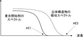
- the relationship between the UV-visible absorption spectra of the polymerization initiator A and the steric structure is shown in FIG.
- the absorption edge AE1 on the long wavelength side of the ultraviolet-visible absorption spectrum of the polymerization initiator A is located on the shorter wavelength side than the absorption edge AE2 on the long wavelength side of the ultraviolet-visible absorption spectrum of the three-dimensional structure. . That is, the absorption wavelength range of the polymerization initiator A overlaps with the absorption wavelength range of the three-dimensional structure. Therefore, in such an embodiment, as shown in FIG.
- light to which the polymerization initiator A is exposed to the plating layer precursor layer disposed on the three-dimensional structure Is also a wavelength on the short wavelength side and is a light of a wavelength to which the polymerization initiator A is sensitive, in other words, when it is irradiated with a light having a wavelength on the short wavelength side of the absorption edge AE1 of the polymerization initiator A). It is possible to suppress the reflected light generated in the three-dimensional structure, and it is possible to suppress the exposure in the non-exposure part caused by this.
- the first embodiment of the method for producing a conductive laminate is Step of obtaining a three-dimensional substrate to be plated layer precursor layer having a three-dimensional substrate having a three-dimensional shape (three-dimensional shape) including a curved surface, and a to-be-plated layer precursor layer disposed on the three-dimensional substrate A step of obtaining a three-dimensional substrate with a plating layer precursor layer), The pattern exposure is performed by irradiating a light to a wavelength shorter than the absorption edge on the long wavelength side of the UV-visible absorption spectrum of the three-dimensional substrate with respect to the precursor layer to be plated and to which the polymerization initiator is sensitive.
- Step 2 Forming the patterned layer to be plated by curing the exposed portion (Step 2: obtaining a three-dimensional substrate with the patterned layer to be plated); And performing a plating process on the patterned layer to form a patterned metal layer on the patterned layer (step 3: metal layer forming step (conductive laminate forming step)).
- step 3 metal layer forming step (conductive laminate forming step)
- the absorption edge on the long wavelength side of the UV-visible absorption spectrum of the polymerization initiator contained in the plating layer precursor layer is on the long wavelength side of the ultraviolet-visible absorption spectrum of the three-dimensional substrate. The wavelength is shorter than the absorption edge. This relationship corresponds to the relationship described in FIG. FIG.
- FIG. 3 is a perspective view schematically showing a conductive laminate 30 formed by the first embodiment of the method for producing a conductive laminate of the present invention
- FIG. 4 is a partial cross-sectional view thereof.
- the conductive laminate 30 has a three-dimensional substrate 11 having a three-dimensional shape including a curved surface, a pattern-like to-be-plated layer 13 disposed on the surface 11 a of a region having a three-dimensional shape including a curved surface of the three-dimensional substrate 11 And a patterned metal layer 14 disposed on the layer 13 to be plated.
- the metal layer 14 is a layer which extends in a first direction (Y direction) and is arranged at a predetermined interval in a second direction (X direction) orthogonal to the first direction.
- the conductive laminated body 30 shown in FIG. 3 arrange
- substrate 11 of course, arrange
- metal layers 14 may be disposed on both sides of the three-dimensional substrate 11.
- the three-dimensional structure in the present invention is of course limited to this structure It will not be done.
- the three-dimensional structure in the present invention may be, for example, a substrate having a three-dimensional shape as shown in FIGS. 3 and 4 or a prismatic or ball (spherical) structure.
- a three-dimensional substrate having a three-dimensional shape is preferable, and a three-dimensional substrate having a three-dimensional shape including a curved surface is more preferable.
- the transmittance (%) of the three-dimensional structure and the position of the absorption edge on the long wavelength side of the UV-visible absorption spectrum are synonymous with the range of each parameter of the three-dimensional substrate described in the first embodiment.
- the material of the three-dimensional structure is also the same as the various materials described in the first embodiment.
- the polymerization initiator contained in the precursor layer to be plated and the light absorption characteristics of the three-dimensional substrate and the wavelength of the light to be irradiated in the exposure step of the step 2, as an example of the exposure conditions, the polymerization initiator contained in the precursor layer to be plated and the light absorption characteristics of the three-dimensional substrate and the wavelength of the light to be irradiated
- the form which controls is described, of course, it is not limited to this. That is, the method for producing a conductive laminate of the present invention also includes an embodiment which does not control the light absorption characteristics of the polymerization initiator and the three-dimensional substrate contained in the layer to be plated precursor layer and the wavelength of the light to be irradiated.
- Step 1 Step of obtaining a three-dimensional substrate with a to-be-plated layer precursor layer
- Step 1 is a three-dimensional to-be-plated layer precursor layer-containing layer having a three-dimensional substrate having a three-dimensional shape including a curved surface (hereinafter also referred to as “three-dimensional substrate”) and a to-be-plated layer precursor layer disposed on the three-dimensional substrate. It is a process of obtaining a substrate. That is, it is a process of forming the three-dimensional substrate 10 with a to-be-plated layer precursor layer as shown in FIG.
- Step 1 the plating layer precursor layer (unexposed coating film) 12 is disposed on the surface 11 a of the region having a three-dimensional shape including the curved surface of the three-dimensional substrate 11 by, for example, a coating method.
- a coating method for example, various materials and procedures used in step 1 will be described in detail.
- the three-dimensional substrate is not particularly limited as long as it is a substrate having a three-dimensional shape (note that “substrate” means one having two main surfaces).
- Specific examples of the substrate having a three-dimensional shape include a three-dimensional substrate having a three-dimensional shape including a curved surface as shown in FIGS. 3 and 4.
- an insulating material is mentioned, for example.
- the three-dimensional substrate can be formed by molding the resin substrate into a desired three-dimensional shape by a method such as heat molding.
- the adhesive sheet mentioned later is also contained.
- polyester resins polyethylene terephthalate and polyethylene naphthalate etc.
- polyether sulfone resins examples include polyester resins (polyethylene terephthalate and polyethylene naphthalate etc.), polyether sulfone resins, poly (meth) acrylic resins, polyurethane resins, polycarbonate resins, polysulfone resins, polyamide resins Resin, polyarylate resin, polyolefin resin, cellulose resin, polyvinyl chloride resin, cycloolefin resin, etc. may be mentioned.
- polyester resins for example, polyethylene terephthalate and polyethylene naphthalate etc.
- polyolefin resins are preferable.
- the poly (meth) acrylic resin means a polyacrylic resin or a polymethacrylic resin.
- an adhesive substrate that is, an adhesive sheet may be used as the resin substrate.
- Well-known materials an acrylic adhesive, a silicone adhesive, etc.
- the thickness (mm) of the three-dimensional substrate is not particularly limited, but is preferably 0.01 to 2 mm, more preferably 0.02 to 1 mm, and more preferably 0.03 to 0. 1 mm is more preferred. In the case of a glass substrate, the thickness is preferably 0.01 to 2 mm, more preferably 0.3 to 0.8 mm, and still more preferably 0.4 to 0.7 mm.
- the three-dimensional substrate is preferably excellent in transparency, and its transmittance (%) is preferably 80% or more, preferably 85% or more, and 90% or more at a wavelength of 400 nm. More preferably, it is particularly preferably 95% or more.
- the transmittance can be measured using an ultraviolet visible near infrared spectrophotometer V-7200F (manufactured by JASCO Corporation).
- V-7200F ultraviolet visible near infrared spectrophotometer
- the position of the absorption edge on the long wavelength side of the UV-visible absorption spectrum of the three-dimensional substrate is longer than the absorption edge on the long wavelength side of the UV-visible absorption spectrum of the polymerization initiator contained in the plating layer precursor layer It is desirable to be in
- the position of the absorption end on the long wavelength side of the UV-visible absorption spectrum of the three-dimensional substrate is not particularly limited, but is preferably 400 nm or less, and is 380 nm or less in terms of excellent transparency and visibility of the conductive laminate to be formed. Is more preferably, and 320 nm or less.
- the lower limit is not particularly limited, but is often 250 nm or more in terms of material properties.
- the absorption edge on the long wavelength side of the UV-visible absorption spectrum of the three-dimensional substrate means the one whose absorbance is 1.0 or less when the UV-visible absorption spectrum of the three-dimensional substrate is measured by UV-3000 (Shimadzu Corporation) Intended for the longer wavelength side.
- the three-dimensional substrate may contain an ultraviolet absorber.
- the ultraviolet absorber By including the ultraviolet absorber, the absorption edge of the ultraviolet and visible absorption spectrum of the three-dimensional substrate moves to the longer wavelength side, and the absorption of the ultraviolet and visible absorption spectrum of the polymerization initiator contained in the plating layer precursor layer described later It is easy to be located on the longer wavelength side than the end.
- the ultraviolet absorber which has an absorption edge in the long wavelength side rather than the absorption edge in the long wavelength side of the ultraviolet visible absorption spectrum of the polymerization initiator contained in the to-be-plated layer precursor layer mentioned later is selected. It is preferable to do.
- the absorption edge on the long wavelength side of the UV-visible absorption spectrum of the ultraviolet absorber used is longer than the absorption edge on the long wavelength side of the UV-visible absorption spectrum of the polymerization initiator contained in the plating layer precursor layer It is preferable to be on the wavelength side.
- substrate at the time of using an ultraviolet absorber also has the same procedure as the above.
- UV absorber to be used is not particularly limited, and known UV absorbers can be used.
- salicylic acid UV absorber for example, salicylic acid UV absorber, benzophenone UV absorber, benzotriazole UV absorber, cyanoacrylate UV absorber And benzoate based ultraviolet light absorbers, malonic acid ester based ultraviolet light absorbers, oxalic acid anilide based ultraviolet light absorbers and the like.
- salicylic acid ultraviolet absorber include phenyl salicylate, p-tert-butylphenyl salicylate, and p-octylphenyl salicylate.
- benzophenone-based UV absorbers examples include 2,4-dihydroxybenzophenone, 2-hydroxy-4-methoxybenzophenone, 2-hydroxy-4-octoxybenzophenone, 2-hydroxy-4-dodecyloxybenzophenone, and 2,2'-.
- the three-dimensional substrate may have a single-layer structure or a multi-layer structure.
- examples of the substrate structure include a laminate having a support and an ultraviolet absorbing layer containing an ultraviolet absorber disposed on the support.
- the support may or may not contain the ultraviolet light absorber.
- the ultraviolet absorbing layer contains at least an ultraviolet absorber.
- binders such as resin, may be contained in the ultraviolet absorber.
- the to-be-plated layer precursor layer is a layer having a functional group that interacts with the plating catalyst or its precursor and a polymerizable group, and is cured in a pattern by exposure described later to be a pattern-like layer to be plated . It is preferable that the to-be-plated layer precursor layer contains at least a polymerization initiator and the following compound X or composition Y. More specifically, the to-be-plated layer precursor layer may be a layer containing a polymerization initiator and the compound X, or may be a layer containing a polymerization initiator and the composition Y.
- Compound X functional group that interacts with a plating catalyst or its precursor (hereinafter, also simply referred to as “interactive group”), and a compound having a polymerizable group
- Composition Y interaction with a plating catalyst or its precursor
- Polymerization initiator There is no restriction
- the polymerization initiator it is preferable to use an initiator whose absorption end on the long wavelength side of the ultraviolet-visible absorption spectrum is located on a shorter wavelength side than the absorption end on the long wavelength side of the ultraviolet-visible absorption spectrum of the three-dimensional substrate described above. .
- polymerization initiators examples include benzophenones, acetophenones, ⁇ -aminoalkylphenones, benzoins, ketones, thioxanthones, benzyls, benzil ketals, oxsim esters, ansolones, tetramethylthiuram monosulfide And bisacyl phosphinxides, acyl phosphine oxides, anthraquinones, azo compounds and the like, and derivatives thereof.
- the absorption end of the UV-visible absorption spectrum of the polymerization initiator means a solution having a concentration of 0.01% by mass of the polymerization initiator (as a solvent, a solvent in which the polymerization initiator is dissolved, for example, acetonitrile is used)
- a solvent a solvent in which the polymerization initiator is dissolved, for example, acetonitrile is used
- the wavelength on the longest wavelength side where the absorbance is 1.0 or less is intended.
- the absorption edge on the long wavelength side of the UV-visible absorption spectrum of the polymerization initiator is located on the shorter wavelength side than the absorption edge on the long wavelength side of the ultraviolet-visible absorption spectrum of the three-dimensional substrate
- the upper limit is not particularly limited, but is often about 150 nm.
- the content of the polymerization initiator in the layer to be plated is not particularly limited, but in terms of the curability of the layer to be plated, it is 0.01 to 5% by mass with respect to the total mass of the layer to be plated And preferably 0.1 to 3% by mass.
- the compound X is a compound having an interactive group and a polymerizable group.
- the interactive group intends a functional group capable of interacting with the plating catalyst or its precursor applied to the pattern-like plating layer, and for example, a functional group capable of forming an electrostatic interaction with the plating catalyst or its precursor
- a nitrogen-containing functional group, a sulfur-containing functional group, an oxygen-containing functional group or the like capable of forming a coordination with a group or a plating catalyst or a precursor thereof can be used.
- ionic polar groups such as carboxylic acid groups, sulfonic acid groups, phosphoric acid groups, and boronic acid groups, ether groups, or the like because they have high polarity and high adsorption ability to a plating catalyst or a precursor thereof, etc.
- a cyano group is preferred, and a carboxylic acid group (carboxyl group) or a cyano group is more preferred.
- the compound X may contain two or more interactive groups.
- the polymerizable group is a functional group capable of forming a chemical bond by energy application, and examples thereof include a radically polymerizable group and a cationically polymerizable group. Among them, a radically polymerizable group is preferable from the viewpoint of more excellent reactivity.
- a radically polymerizable group for example, acrylic acid ester group (acryloyloxy group), methacrylic acid ester group (methacryloyloxy group), itaconic acid ester group, crotonic acid ester group, isocrotonic acid ester group, and maleic acid ester group
- acrylic acid ester group acryloyloxy group
- methacrylic acid ester group methacryloyloxy group
- itaconic acid ester group crotonic acid ester group
- isocrotonic acid ester group isocrotonic acid ester group
- maleic acid ester group for example, acrylic acid ester group (acryloyloxy group), methacrylic acid ester group (methacryloyloxy group), itaconic acid ester group, crotonic acid ester group, isocrotonic acid ester group, and maleic acid ester group
- unsaturated carboxylic acid ester groups such as, styryl group, vinyl group, acrylamide group
- the compound X may contain two or more types of polymerizable groups.
- the number of polymerizable groups contained in the compound X is not particularly limited, and may be one or two or more.
- the compound X may be a low molecular weight compound or a high molecular weight compound.
- the low molecular weight compound intends a compound having a molecular weight of less than 1000
- the high molecular weight compound intends a compound having a molecular weight of 1000 or more.
- the low molecular weight compound which has the said polymeric group corresponds to what is called a monomer (monomer).
- the polymer compound may be a polymer having a predetermined repeating unit.
- only 1 type may be used and 2 or more types may be used together.
- the weight-average molecular weight of the polymer is not particularly limited, but is preferably 1000 or more and 700,000 or less, more preferably 2000 or more and 200,000 or less, in terms of more excellent handleability such as solubility. In particular, from the viewpoint of polymerization sensitivity, 20000 or more is more preferable.
- the synthesis method of the polymer having such a polymerizable group and interactive group is not particularly limited, and known synthesis methods (see paragraphs [0097] to [0125] of Patent Publication 2009-280905) are used.
- the weight average molecular weight of the polymer can be measured by the GPC method (gel permeation chromatography).
- GPC method uses HLC-8020GPC (made by Tosoh Corp.), TSKgel SuperHZM-H, TSKgel SuperHZ4000, TSKgel SuperHZ 2000 (made by Tosoh Corp., 4.6 mm ID ⁇ 15 cm) as columns, THF (tetrahydrofuran as the eluent) Based on the method using
- a repeating unit having a polymerizable group represented by the following formula (a) (hereinafter, appropriately referred to as a polymerizable group unit) and an interaction represented by the following formula (b)
- Examples include copolymers containing repeating units having a nature group (hereinafter also referred to as interaction group units as appropriate).
- R 1 to R 5 each independently represent a hydrogen atom or a substituted or unsubstituted alkyl group (eg, methyl group, ethyl group, propyl group, and butyl group) Group etc.).
- the type of substituent is not particularly limited, and examples thereof include a methoxy group, a chlorine atom, a bromine atom, and a fluorine atom.
- R 1 a hydrogen atom, a methyl group or a methyl group substituted with a bromine atom is preferable.
- R 2 a hydrogen atom, a methyl group or a methyl group substituted with a bromine atom is preferable.
- R 3 a hydrogen atom is preferable.
- R 4 a hydrogen atom is preferable.
- R 5 a hydrogen atom, a methyl group or a methyl group substituted with a bromine atom is preferable.
- X, Y and Z each independently represent a single bond or a substituted or unsubstituted divalent organic group.
- divalent organic group a substituted or unsubstituted divalent aliphatic hydrocarbon group (preferably having a carbon number of 1 to 8; for example, an alkylene group such as a methylene group, an ethylene group, and a propylene group), a substituted or non-substituted Substituted divalent aromatic hydrocarbon group (preferably having a carbon number of 6 to 12.
- phenylene group For example, phenylene group), -O-, -S-, -SO 2- , -N (R)-(R: alkyl group) And -CO-, -NH-, -COO-, -CONH-, and groups combining these (eg, alkyleneoxy group, alkyleneoxy carbonyl group, alkylene carbonyloxy group, etc.) and the like.
- O- or a substituted or unsubstituted divalent aromatic hydrocarbon group is preferable, and a single bond, an ester group (-COO-) or an amido group (-CONH-) is more preferable.
- L 1 and L 2 each independently represent a single bond or a substituted or unsubstituted divalent organic group.
- a bivalent organic group it is synonymous with the bivalent organic group described by X, Y, and Z mentioned above.
- L 1 an aliphatic hydrocarbon group or a divalent organic group having a urethane bond or a urea bond (for example, an aliphatic hydrocarbon) in that the synthesis of the polymer is easy and the adhesion of the metal layer is more excellent Group is preferable, and those having 1 to 9 carbon atoms in total are more preferable.
- the total number of carbon atoms of L 1 means the total number of carbon atoms contained in the divalent organic group or a substituted or unsubstituted represented by L 1.
- L 2 is a single bond, a divalent aliphatic hydrocarbon group, a divalent aromatic hydrocarbon group, or a combination of these in that the adhesion of the metal layer is more excellent. Is preferred. Among them, L 2 is more preferably a single bond or a total of 1 to 15 carbon atoms. In addition, it is preferable that a divalent organic group is unsubstituted. Incidentally, the total number of carbon atoms of L 2, means the total number of carbon atoms contained in the divalent organic group or a substituted or unsubstituted represented by L 2.
- W represents an interactive group.
- the definition of the interactive group is as described above.
- the content of the polymerizable group unit is preferably 5 to 50 mol% with respect to all the repeating units in the polymer, from the viewpoint of reactivity (curability or polymerization) and suppression of gelation in synthesis. 5 to 40 mol% is more preferable. Further, the content of the above-mentioned interactive group unit is preferably 5 to 95 mol%, more preferably 10 to 95 mol%, with respect to all repeating units in the polymer from the viewpoint of adsorption to the plating catalyst or its precursor. More preferable.
- the repeating unit represented by Formula (A) is the same as the repeating unit represented by said Formula (a), and description of each group is also the same.
- R 5, X and L 2 in the repeating unit represented by formula (B) is the same as R 5, X and L 2 in the repeating unit represented by formula (b), a description of each group Is also the same.
- Wa in the formula (B) represents a group which interacts with the plating catalyst or the precursor thereof, excluding the hydrophilic group represented by V described later or the precursor group thereof. Among these, a cyano group or an ether group is preferable.
- each R 6 independently represents a hydrogen atom or a substituted or unsubstituted alkyl group.
- U represents a single bond or a substituted or unsubstituted divalent organic group.
- the definition of the divalent organic group is the same as the divalent organic group represented by X, Y and Z described above.
- U the synthesis of the polymer is easy and the adhesion of the metal layer is more excellent, and a single bond, an ester group (-COO-), an amide group (-CONH-), an ether group (-O-), or Preferred is a substituted or unsubstituted divalent aromatic hydrocarbon group.
- L 3 represents a single bond or a substituted or unsubstituted divalent organic group.
- the definition of the divalent organic group is the same as the divalent organic group represented by L 1 and L 2 described above.
- L 3 a single bond or a divalent aliphatic hydrocarbon group, a divalent aromatic hydrocarbon group, or a combination thereof is used in that the polymer synthesis is easy and the adhesion of the metal layer is more excellent. Is preferred.
- V represents a hydrophilic group or a precursor group thereof.
- the hydrophilic group is not particularly limited as long as it is a group exhibiting hydrophilicity, and examples thereof include a hydroxyl group and a carboxylic acid group.
- a precursor group of a hydrophilic group means a group which generates a hydrophilic group by a predetermined treatment (for example, treatment with an acid or an alkali), for example, a carboxyl protected with THP (2-tetrahydropyranyl group) And the like.
- the hydrophilic group is preferably an ionic polar group in terms of interaction with the plating catalyst or the precursor thereof.
- the ionic polar group examples include a carboxylic acid group, a sulfonic acid group, a phosphoric acid group, and a boronic acid group.
- a carboxylic acid group is preferable from the viewpoint of appropriate acidity (does not decompose other functional groups).
- the preferred content of each unit in the second preferred embodiment of the above-mentioned polymer is as follows.
- the content of the repeating unit represented by the formula (A) is 5 to 50 with respect to all repeating units in the polymer from the viewpoint of reactivity (curing or polymerization) and suppression of gelation in synthesis.
- the mole% is preferred, and 5 to 30 mole% is more preferred.
- the content of the repeating unit represented by the formula (B) is preferably 5 to 75 mol%, more preferably 10 to 70 mol, based on all the repeating units in the polymer, from the viewpoint of adsorption to the plating catalyst or its precursor. % Is more preferable.
- the content of the repeating unit represented by the formula (C) is preferably 10 to 70% by mole, and more preferably 20 to 60% by mole, based on all repeating units in the polymer, from the viewpoint of developability with aqueous solution and moisture adhesion. Is more preferable, and 30 to 50 mol% is more preferable.
- This polymer can be produced by known methods, such as those in the literature listed above.
- R 11 to R 13 each independently represent a hydrogen atom or a substituted or unsubstituted alkyl group.
- the unsubstituted alkyl group include a methyl group, an ethyl group, a propyl group and a butyl group.
- a substituted alkyl group a methyl group, an ethyl group, a propyl group, and a butyl group substituted by the methoxy group, a chlorine atom, a bromine atom, or a fluorine atom etc. are mentioned.
- R 11 a hydrogen atom or a methyl group is preferable.
- R 12 a hydrogen atom is preferable.
- R 13 a hydrogen atom is preferable.
- L 10 represents a single bond or a divalent organic group.
- a divalent organic group a substituted or unsubstituted aliphatic hydrocarbon group (preferably having a carbon number of 1 to 8), a substituted or unsubstituted aromatic hydrocarbon group (preferably having a carbon number of 6 to 12), -O -, -S-, -SO 2- , -N (R)-(R: alkyl group), -CO-, -NH-, -COO-, -CONH-, or a combination thereof (eg, alkylene An oxy group, an alkylene oxycarbonyl group, an alkylene carbonyloxy group etc. etc. are mentioned.
- a substituted or unsubstituted aliphatic hydrocarbon group a methylene group, an ethylene group, a propylene group, or a butylene group, or these groups are substituted by a methoxy group, a chlorine atom, a bromine atom, or a fluorine atom etc. Is preferred.
- the substituted or unsubstituted aromatic hydrocarbon group an unsubstituted phenylene group or a phenylene group substituted with a methoxy group, a chlorine atom, a bromine atom, a fluorine atom or the like is preferable.
- one of the preferred embodiments of L 10 includes —NH—aliphatic hydrocarbon group— or —CO—aliphatic hydrocarbon group—.
- W is the same as the definition of W in Formula (b), and represents an interactive group.
- the definition of the interactive group is as described above.
- Formula (X) as a preferable aspect of W, an ionic polar group is mentioned, and a carboxylic acid group is preferable.
- Q represents an n-valent linking group
- Ra represents a hydrogen atom or a methyl group
- n represents an integer of 2 or more.
- R a represents a hydrogen atom or a methyl group, preferably a hydrogen atom.
- the valence n of Q is 2 or more, preferably 2 or more and 6 or less, more preferably 2 or more and 5 or less, from the viewpoint of further improving the adhesion between the three-dimensional substrate and the metal layer. More preferably, it is 4 or less.
- the n-valent linking group represented by Q for example, a group represented by the formula (1A), a group represented by the formula (1B),
- -NH-, -NR (R: represents an alkyl group)-, -O-, -S-, a carbonyl group, an alkylene group, an alkenylene group, an alkynylene group, a cycloalkylene group, an aromatic group, and a heterocyclic group, And the group which combined these 2 or more types is mentioned.
- JP2013-43946A The compounds represented by the formula (X) are described in paragraphs [0019] to [0034] of JP2013-43946A and paragraphs [0070] to [0080] etc. of JP2013-43945A. Can be referred to as appropriate.
- Composition Y is a composition containing a compound having an interactive group and a compound having a polymerizable group. That is, the to-be-plated layer precursor layer contains two types of the compound which has an interactive group, and the compound which has a polymeric group. The definition of the interactive group and the polymerizable group is as described above. The definition of the interactive group contained in the compound having an interactive group is as described above. Such a compound may be a low molecular weight compound or a high molecular weight compound. As a preferred embodiment of the compound having an interactive group, a polymer having a repeating unit represented by the above-mentioned formula (b) (for example, polyacrylic acid) can be mentioned.
- b polymer having a repeating unit represented by the above-mentioned formula (b) (for example, polyacrylic acid)
- the compound having an interactive group preferably does not contain a polymerizable group.
- the compound having a polymerizable group is a so-called monomer, and is preferably a polyfunctional monomer having two or more polymerizable groups in that the hardness of the formed pattern-like layer to be plated is more excellent.
- the polyfunctional monomer it is preferable to use a monomer having 2 to 6 polymerizable groups.
- the molecular weight of the polyfunctional monomer to be used is preferably 150 to 1000, more preferably 200 to 700, from the viewpoint of molecular mobility during the crosslinking reaction that affects the reactivity.
- the distance (distance) between the plurality of polymerizable groups is preferably 1 to 15 in terms of the number of atoms, and more preferably 6 or more and 10 or less.
- a polyfunctional monomer the compound represented by Formula (1) mentioned above is mentioned.
- the compound having a polymerizable group may contain an interactive group.
- the mass ratio of the compound having an interactive group to the compound having a polymerizable group is not particularly limited, but the pattern to be formed is In view of the balance between the strength of the plating layer and the plating suitability, 0.1 to 10 is preferable, and 0.5 to 5 is more preferable.
- the content of the compound X (or the composition Y) in the layer-to-be-plated precursor layer is not particularly limited, but preferably 50% by mass or more, and 80% by mass or more based on the total mass of the layer-to-be-plated precursor layer. More preferable.
- the upper limit is not particularly limited, but is preferably 99.5% by mass or less.
- the to-be-plated layer precursor layer may contain components other than the polymerization initiator and the compound X or the composition Y.
- the to-be-plated layer precursor layer may contain a monomer (except the compound represented by the above formula (1)). By including the monomer, it is possible to appropriately control the crosslinking density and the like in the pattern-like layer to be plated.
- the monomer to be used is not particularly limited, and examples of the compound having addition polymerization include compounds having an ethylenically unsaturated bond, and compounds having ring opening polymerization include a compound having an epoxy group and the like.
- the polyfunctional monomer means a monomer having two or more polymerizable groups. Specifically, it is preferable to use a monomer having 2 to 6 polymerizable groups.
- additives eg, sensitizer, curing agent, polymerization inhibitor, antioxidant, antistatic agent, filler, particles, flame retardant, surfactant, lubricant, and plastic
- An agent etc. may be added as needed.
- the method of arranging the layer to be plated precursor layer on the three-dimensional substrate is not particularly limited, and a composition containing the above-mentioned various components is coated on the three-dimensional substrate to form a layer to be plated precursor layer.
- the method to form (coating method) or the method (transfer method) of forming a to-be-plated layer precursor layer on a temporary substrate, and transferring on both surfaces of a three-dimensional substrate, etc. are mentioned.
- the coating method is preferable in that the thickness can be easily controlled.
- the aspect of the coating method is explained in full detail.
- the composition used in the coating method contains at least the above-mentioned polymerization initiator and the compound X or the composition Y.
- the other components described above may be included as needed.
- the composition preferably contains a solvent.
- the solvent which can be used is not particularly limited, and, for example, water; alcohol solvents such as methanol, ethanol, propanol, ethylene glycol, 1-methoxy-2-propanol, glycerin, and propylene glycol monomethyl ether; acids such as acetic acid; Ketone solvents such as methyl ethyl ketone and cyclohexanone; amide solvents such as formamide, dimethylacetamide and N-methyl pyrrolidone; nitrile solvents such as acetonitrile and propionitrile; ester solvents such as methyl acetate and ethyl acetate; Other solvents include carbonate solvents such as dimethyl carbonate and diethyl carbonate; ether solvents, glyco
- alcohol solvents amide solvents, ketone solvents, nitrile solvents or carbonate solvents are preferable.
- the content of the solvent in the composition is not particularly limited, but is preferably 50 to 98% by mass, and more preferably 70 to 95% by mass, with respect to the total amount of the composition. If it is in the said range, it is excellent in the handleability of a composition, and control of a layer thickness etc. is easy to be performed.
- a composition may be apply
- the conditions for the drying treatment are not particularly limited, but it is preferable to carry out the treatment at room temperature to 220 ° C. (preferably 50 to 120 ° C.) for 1 to 30 minutes (preferably 1 to 10 minutes) in terms of more excellent productivity. .
- the thickness of the precursor layer to be plated is not particularly limited, but is preferably 0.01 to 20 ⁇ m, more preferably 0.1 to 10 ⁇ m, and still more preferably 0.1 to 5 ⁇ m.
- substrate and a to-be-plated layer precursor layer may be contained in the said three-dimensional board
- a primer layer may be disposed between the three-dimensional substrate and the to-be-plated layer precursor layer.
- a low molecular weight layer or a polymer layer close to the surface energy of the patterned plating layer can be used.
- a low molecular weight layer or a high molecular weight layer having a polymerization active site can be used.
- a rubber resin or the like having a low elastic modulus can be used.
- the thickness of the primer layer is not particularly limited, but generally 0.01 to 100 ⁇ m is preferable, 0.05 to 20 ⁇ m is more preferable, and 0.05 to 10 ⁇ m is still more preferable.
- the material in particular of a primer layer is not restrict
- a thermosetting resin, a thermoplastic resin, or a mixture thereof may be used.
- the thermosetting resin include epoxy resins, phenol resins, polyimide resins, polyester resins, bismaleimide resins, polyolefin resins, and isocyanate resins.
- thermoplastic resin for example, phenoxy resin, polyether sulfone resin, polysulfone resin, polyphenylene sulfone resin, polyphenylene sulfide resin, polyphenyl ether resin, polyetherimide resin, and ABS resin (acrylonitrile (acrylonitrile) -Butadiene-styrene copolymer) and the like.
- the thermoplastic resin and the thermosetting resin may be used alone or in combination of two or more.
- a resin containing a cyano group may be used.
- an ABS resin or a unit having a cyano group in a side chain described in JP-A-2010-84196 [0039] to [0063] may be used.
- Polymer containing may be used.
- rubber components such as NBR rubber (acrylonitrile butadiene rubber) and SBR rubber (styrene butadiene rubber) can also be used.
- the conjugated diene compound unit means a repeating unit derived from a conjugated diene compound.
- the conjugated diene compound is not particularly limited as long as it is a compound having a molecular structure having two carbon-carbon double bonds separated by one single bond.
- One of the preferable embodiments of the repeating unit derived from the conjugated diene compound is a repeating unit generated by the polymerization reaction of a compound having a butadiene skeleton.
- the conjugated diene compound unit may be hydrogenated, and when it contains a hydrogenated conjugated diene compound unit, the adhesion of the patterned metal layer is further improved, which is preferable. That is, the double bond in the repeating unit derived from the conjugated diene compound may be hydrogenated.
- the polymer having the conjugated diene compound unit which may be hydrogenated may contain the above-mentioned interactive group.
- Preferred embodiments of this polymer include acrylonitrile-butadiene rubber (NBR), carboxyl group-containing nitrile rubber (XNBR), acrylonitrile-butadiene-isoprene rubber (NBIR), ABS resin, and hydrogenated products thereof (for example, hydrogen) Added acrylonitrile-butadiene rubber) and the like.
- NBR acrylonitrile-butadiene rubber
- XNBR carboxyl group-containing nitrile rubber
- NBIR acrylonitrile-butadiene-isoprene rubber
- ABS resin and hydrogenated products thereof (for example, hydrogen) Added acrylonitrile-butadiene rubber) and the like.
- the primer layer contains other additives (eg, sensitizers, antioxidants, antistatic agents, UV absorbers, fillers, particles, flame retardants, surfactants, lubricants, plasticizers, etc.) May be included.
- additives eg, sensitizers, antioxidants, antistatic agents, UV absorbers, fillers, particles, flame retardants, surfactants, lubricants, plasticizers, etc.
- the method for forming the primer layer is not particularly limited, and a method of laminating a resin to be used on a three-dimensional substrate, or a solution obtained by dissolving necessary components in a soluble solvent is applied to a three-dimensional substrate surface
- coating on top and drying is mentioned.
- the heating temperature and time in the coating method may be selected as long as the coating solvent can be sufficiently dried, but from the viewpoint of production suitability, the heating temperature is preferably 200 ° C. or less and the heating time is preferably 60 minutes or less. It is more preferable that the reaction be performed at a temperature of 100 ° C. for 20 minutes or less.
- an optimum solvent for example, cyclohexanone and methyl ethyl ketone etc. is appropriately selected according to the resin to be used.
- Step 2 Three-dimensional Substrate Forming Process with Patterned Plated Layer
- This process 2 is a process which exposes in a pattern shape with respect to a to-be-plated layer precursor layer, and hardens an exposure part.
- the irradiation light in the above exposure corresponds to light of a wavelength shorter than the absorption edge on the long wavelength side of the UV-visible absorption spectrum of the substrate and to which the polymerization initiator is sensitive.
- the non-irradiated area of the layer to be plated formation is further removed to form a pattern-like layer to be plated.
- light of a wavelength to which the polymerization initiator is exposed is irradiated to a predetermined irradiation area (opening area of the photomask 25) of the layer precursor layer 12 to be plated.
- the light irradiated to the to-be-plated layer precursor layer 12 is absorbed by the three-dimensional substrate 11, so that reflection is less likely to occur on the substrate surface even in a region with particularly large curvature.
- the pattern-like to-be-plated layer 13 (see FIG. 7) of the three-dimensional substrate 20 with a pattern-like to-be-plated layer formed by the above steps is a plating catalyst or a precursor thereof in Step 3 described later.
- Adsorb (adhere). That is, the pattern-like to-be-plated layer 13 functions as a good receptive layer of a plating catalyst or its precursor.
- the polymeric group which the to-be-plated layer precursor layer 12 had was utilized for the coupling
- the method in particular to pattern-wise expose the to-be-plated layer precursor layer on a three-dimensional substrate is not restrict
- the method of irradiating an actinic ray or radiation is mentioned.
- actinic light UV (ultraviolet) lamp, light irradiation with visible light and the like, and the like are used.
- the light source include a mercury lamp, a metal halide lamp, a xenon lamp, a chemical lamp, and a carbon arc lamp.
- an electron beam, an X-ray, an ion beam, far infrared rays, etc. are mentioned.
- pattern exposure on a coating film on a three-dimensional substrate include scanning exposure with an infrared laser, high-intensity flash exposure such as a xenon discharge lamp using a mask, or infrared lamp exposure using a mask Preferably it is mentioned.
- the polymerizable group contained in the compound in the layer-to-be-plated layer precursor layer is activated, crosslinking between the compounds occurs, and curing of the layer proceeds.
- the exposure energy long 10 ⁇ 8000mJ / cm 2 approximately, and preferably from 50 ⁇ 3000mJ / cm 2.
- the method in particular which implements the said exposure process to pattern shape is not restrict
- a photomask it is preferable to use a photomask having a three-dimensional shape corresponding to the surface shape of the layer-to-be-plated precursor layer disposed on the three-dimensional substrate and having an opening.
- the photomask is obtained, for example, by molding and processing a flat thermoplastic resin film into a three-dimensional shape corresponding to the surface shape of the layer-to-be-plated precursor layer disposed on the three-dimensional substrate.
- the forming method is not particularly limited, and examples thereof include a vacuum forming method and a press forming method. From the viewpoint of maintaining the accuracy of the pattern formed on the mask, a method using a jig is preferable.
- the thermoplastic resin film to be molded is softened by heating, and then the above-mentioned softened film is placed on the jig and vacuum drawing is performed,
- tool is mentioned.
- the molding temperature is preferably 100 ° C. or more, more preferably 150 ° C. or more, and 300 ° C. or less from the viewpoint of durability of the film from the viewpoint of accurately molding the shape as a jig. It is preferable that it is 250 degrees C or less.
- the unexposed part in the to-be-plated layer precursor layer 12 is removed, and the pattern-like to-be-plated layer 13 is formed.
- the removal method is not particularly limited, and an optimum method is appropriately selected depending on the compound to be used.
- a method of using an alkaline solution (preferably pH: 13.0-13.8) as a developer can be mentioned.
- the method (immersion method) of making the three-dimensional substrate which has the to-be-plated layer precursor layer which was exposed in a solution (immersion method), and the to-be-plated layer precursor layer exposed is mentioned, the immersion method is preferable.
- the immersion time is preferably about 1 to 30 minutes from the viewpoint of productivity and workability.
- a method in which a solvent in which a compound to be used is dissolved is used as a developer and is immersed therein.
- a pattern-like to-be-plated layer is a layer containing the interactive group mentioned above. As described later, the pattern-like plated layer is plated.
- the thickness of the pattern-like to-be-plated layer formed by the above treatment is not particularly limited, it is preferably 0.01 to 10 ⁇ m, more preferably 0.2 to 5 ⁇ m, and 0.3 to 1.0 ⁇ m from the viewpoint of productivity. More preferable.
- FIG. 8 is a partially enlarged top view of the pattern-like to-be-plated layer, and the pattern-like to-be-plated layer is composed of a plurality of thin lines 31 and is a mesh pattern including a plurality of grids 32 of intersecting thin lines 31.
- the length W of one side of the lattice (opening) in the mesh pattern is preferably 800 ⁇ m or less, more preferably 600 ⁇ m or less, preferably 50 ⁇ m or more, and more preferably 400 ⁇ m or more.
- the lattice 32 has a substantially rhombus shape. However, in addition to this, it may have a polygonal shape (for example, a triangle, a quadrangle, a hexagon or a random polygon).
- the shape of one side may be a curved shape other than a linear shape, or may be an arc shape.
- the two opposing sides may have an outwardly convex arc shape, and the other two opposing sides may have an inward convex arc shape.
- the shape of each side may be a wavy line shape in which an outward convex arc and an inward convex arc are continuous.
- the shape of each side may be a sine curve.
- FIG. 8 although a pattern-form to-be-plated layer has a mesh-like pattern, it is not limited to this form, As shown in FIG. 9, a stripe pattern may be sufficient.
- the line width of the pattern-like layer to be plated is not particularly limited, it is preferably 30 ⁇ m or less, more preferably 20 ⁇ m or less, and further preferably 15 ⁇ m or less from the viewpoint of the visibility of the metal layer disposed on the pattern-like layer to be plated.
- the thickness is preferably 10 ⁇ m or less, more preferably 9 ⁇ m or less, and most preferably 7 ⁇ m or less.
- 0.5 micrometer or more is preferable and, as for the lower limit, 1.0 micrometer or more is more preferable.
- the area where the pattern-like plated layer is formed is preferably 50 area% or less, more preferably 40 area% or less, and 30 area% or less with respect to the total surface area of the three-dimensional substrate. More preferable.
- Process 3 applies a plating catalyst or its precursor to the pattern-like to-be-plated layer formed in the said process 2, and performs a plating process with respect to the pattern-like to-be-plated layer to which the plating catalyst or its precursor was given. It is a process of forming a metal layer on a pattern-like plating layer. By performing this step, as shown in FIG. 3 and FIG. 4, the metal layer 14 is disposed on the pattern-like layer to be plated 13, and the conductive laminate 30 is obtained.
- step 3-1 the step of applying a plating catalyst or a precursor thereof to the pattern-like layer to be plated
- Step 3-2 the step of plating the pattern-like layer to which the plating catalyst or precursor thereof is applied
- Step 3-1 Catalyst application step
- a plating catalyst or a precursor thereof is applied to the patterned plating layer.
- the interaction group contained in the pattern-like to-be-plated layer mentioned above adheres (adsorbs) the added plating catalyst or its precursor according to the function.
- a plating catalyst or a precursor thereof is applied in the patterned plating layer and on the surface of the patterned plating layer.
- the plating catalyst or a precursor thereof functions as a catalyst or an electrode of the plating process. Therefore, the type of plating catalyst or precursor thereof to be used is appropriately determined depending on the type of plating process.
- the plating catalyst or precursor thereof to be used is preferably an electroless plating catalyst or a precursor thereof.
- Any plating catalyst can be used in this step as long as it becomes an active nucleus at the time of plating.
- Specific examples thereof include metals having a catalytic ability for autocatalytic reduction (known as metals capable of electroless plating having a lower ionization tendency than Ni) and the like.
- Specific examples thereof include Pd, Ag, Cu, Ni, Pt, Au, and Co.
- Ag, Pd, Pt or Cu is preferable from the viewpoint of high catalytic ability.
- a metal colloid may be used as the plating catalyst.
- the plating catalyst precursor used in this step can be used without particular limitation as long as it can be a plating catalyst by a chemical reaction. Mainly, metal ions of the metals listed above as the plating catalyst are used.
- the metal ion which is a plating catalyst precursor becomes a zero-valent metal which is a plating catalyst by a reduction reaction.
- the metal ion which is a plating catalyst precursor may be separately converted to a zero-valent metal by reduction reaction before immersion in a plating bath to be a plating catalyst.
- the plating catalyst precursor may be immersed in the plating bath as it is, and may be changed to a metal (plating catalyst) by a reducing agent in the plating bath.
- the metal ions are preferably applied to the patterned plating layer using a metal salt.
- the metal salt used is not particularly limited as long as it is dissolved in an appropriate solvent and dissociated into metal ions and bases (anions), and M (NO 3 ) n , MCl n , M 2 / n (SO 4 ), and M 3 / n (PO 4 ) (M represents an n-valent metal atom) and the like.
- metal ion what the said metal salt dissociated can be used suitably.
- Specific examples thereof include, for example, Ag ion, Cu ion, Al ion, Ni ion, Co ion, Fe ion, and Pd ion, and among them, those capable of multidentate coordination are preferable and capable of coordination Ag ion or Pd ion is more preferable in terms of the number of functional groups and the catalytic ability.
- a metal salt is dissolved in a suitable solvent, a solution containing dissociated metal ions is prepared, and the solution is applied on the pattern-like to-be-plated layer
- the three-dimensional substrate on which the pattern-like to-be-plated layer is formed may be immersed in the solution.
- Water or an organic solvent is suitably used as the above-mentioned solvent.
- the organic solvent a solvent capable of penetrating the pattern-like plated layer is preferable.
- acetone methyl acetoacetate, ethyl acetoacetate, ethylene glycol diacetate, cyclohexanone, acetylacetone, acetophenone, 2- (1-cyclohexenyl) cyclohexanone
- Propylene glycol diacetate, triacetin, diethylene glycol diacetate, dioxane, N-methyl pyrrolidone, dimethyl carbonate, and dimethyl cellosolve can be used.
- the concentration of the plating catalyst or its precursor in the solution is not particularly limited, but is preferably 0.001 to 50% by mass, and more preferably 0.005 to 30% by mass.
- the contact time is preferably about 30 seconds to 24 hours, and more preferably about 1 minute to 1 hour.
- the amount of adsorption of the plating catalyst of the pattern-like layer to be plated or its precursor varies depending on the type of plating bath used, catalyst metal species, interactive species of pattern-like layer to be plated, and the method of use, etc. From the viewpoint of the precipitation property of the above, 5 to 1000 mg / m 2 is preferable, 10 to 800 mg / m 2 is more preferable, and 20 to 600 mg / m 2 is still more preferable.
- Step 3-2 plating process
- the method of plating treatment is not particularly limited, and examples thereof include electroless plating treatment and electrolytic plating treatment (electroplating treatment).
- the electroless plating treatment may be performed alone, or after the electroless plating treatment is performed, the electrolytic plating treatment may be further performed.
- so-called silver mirror reaction is included as a type of the above-mentioned electroless plating process.
- the metal ions deposited may be reduced by a silver mirror reaction or the like to form a metal layer in a desired pattern, and then an electrolytic plating process may be performed thereafter.
- an electrolytic plating process may be performed thereafter.
- the electroless plating process refers to an operation of depositing a metal by a chemical reaction using a solution in which metal ions to be deposited as plating are dissolved.
- the electroless plating process in this step is performed, for example, by washing the substrate provided with the pattern-like to-be-plated layer to which metal ions have been applied, to remove excess metal ions, and then immersing the substrate in an electroless plating bath.
- a known electroless plating bath can be used. In the electroless plating bath, reduction of metal ions and subsequent electroless plating are performed.
- the reduction of the metal ion in the pattern-like to-be-plated layer prepares a catalyst activation solution (reduction solution) separately from the above-mentioned embodiment using an electroless plating solution, and performs it as another process before the electroless plating process It is also possible.
- the catalyst activation solution is a solution in which a reducing agent capable of reducing metal ions to zero-valent metal is dissolved, and the concentration of the reducing agent relative to the whole solution is preferably 0.1 to 50% by mass, and more preferably 1 to 30% by mass.
- the reducing agent it is possible to use a boron-based reducing agent such as sodium borohydride and dimethylamine borane, formaldehyde, hypophosphorous acid and the like. At the time of immersion, it is preferable to immerse while applying stirring or shaking.
- composition of a general electroless plating bath in addition to a solvent (for example, water), Metal ions for plating; Reductant, 3.
- Additives (stabilizers) which improve the stability of metal ions are mainly included.
- the plating bath may contain known additives such as a stabilizer for the plating bath.
- the organic solvent used in the electroless plating bath needs to be a solvent that can be used in water, and from that point, ketones such as acetone or alcohols such as methanol, ethanol and isopropanol are preferable.
- the immersion time in the electroless plating bath is preferably about 1 minute to 6 hours, and more preferably about 1 minute to 3 hours.
- the electrolytic plating process refers to an operation of depositing a metal by an electric current using a solution in which metal ions to be deposited as plating are dissolved.
- electrolytic plating can be performed after the above-described electroless plating, if necessary.
- the thickness of the pattern-like metal layer to be formed can be appropriately adjusted.
- a conventionally known method can be used as a method of electrolytic plating.
- copper, chromium, lead, nickel, gold, silver, tin, zinc, etc. are mentioned, From a conductive viewpoint, copper, gold, or silver is preferable, and copper Is more preferred.
- the film thickness of the metal layer obtained by the electrolytic plating can be controlled by adjusting the concentration of the metal contained in the plating bath, the current density or the like.
- the conductive laminate 30 obtained according to the first embodiment has a three-dimensional substrate 11 having a hemispherical shape and a pattern-like plated layer 13 on one surface of the three-dimensional substrate 11. And the patterned metal layer 14 disposed on the patterned plating layer 13.
- the conductive laminate 30 can be applied to various applications as described later, but can be applied to, for example, a touch sensor.
- the patterned metal layer 14 can be made to function as a so-called sensor electrode, and if necessary, a lead wire (not shown) is provided at the end of the patterned metal layer 14 It may be electrically connected.
- the thickness of the metal layer formed by the above-mentioned procedure is not particularly limited, and an optimum thickness is appropriately selected according to the purpose of use, but from the viewpoint of the conductive property, it is preferably 0.1 ⁇ m or more Is more preferably 1 to 30 ⁇ m.
- the type of metal constituting the metal layer is not particularly limited, and examples thereof include copper, chromium, lead, nickel, gold, silver, tin and zinc, etc. From the viewpoint of conductivity, copper, gold, Alternatively, silver is preferred, and copper or silver is more preferred.
- the pattern shape of the metal layer is not particularly limited. However, since the metal layer is disposed on the pattern-like layer to be plated, the metal layer is adjusted according to the pattern shape of the pattern-like layer to be plated.
- the metal layer of a mesh pattern can be suitably applied as a sensor electrode in a touch panel.
- the pattern shape is a mesh pattern
- the range of the length W of one side of the lattice (opening) in the mesh pattern, the preferable aspect of the shape of the lattice, and the line width of the metal layer It is the same as the aspect of the plating layer.
- the exposure process has been described as a method for forming the pattern-like plated layer, but the present invention is not limited to this aspect, and another energy application method such as heat treatment is employed. You may
- the metal layer is disposed only on one side of the three-dimensional substrate.
- the present invention is not limited to this embodiment, and the metal layer may be disposed on both sides of the three-dimensional substrate. That is, in the first modification of the first embodiment of the method of manufacturing the conductive laminate, the to-be-plated layer precursor layer is formed on both main surfaces of the three-dimensional substrate to form a to-be-plated layer precursor layer-attached substrate.
- FIG. 10 shows a perspective view of a conductive laminate 40 having metal layers on both main surfaces of a three-dimensional substrate of a three-dimensional substrate, and FIG.
- the metal layer 24A is a layer extending in a first direction (Y direction) and arranged at a predetermined interval in a second direction (X direction) orthogonal to the first direction
- the metal layer 24B is a layer It is a layer which extends in the second direction (X direction) and is arranged at a predetermined interval in the first direction (Y direction) orthogonal to the second direction. That is, in the step of forming the pattern-like to-be-plated layers on both main surfaces of the three-dimensional substrate, the above-mentioned metal layers 24A and 24B are exposed and developed by coating the coating layer precursor layer formed on the three-dimensional substrate.
- the metal layer 24A and the metal layer 24B may extend in a first direction of the touch sensor and a second sensor electrode extending in a second direction. It functions as a sensor electrode.
- Second embodiment the second embodiment of the method for producing a conductive laminate of the present invention will be described in detail.
- the embodiment using the hemispherical three-dimensional substrate has been described, but the present invention is not limited to this embodiment.
- FIG. 12 and FIG. 13 for example, using a three-dimensional substrate 51 having a flat portion 51 a and a curved portion 51 b including curved surfaces disposed on both ends in series with the flat portion 51 a A laminate 50 may be obtained. That is, the conductive laminate 50 of the second embodiment is different from the conductive laminate 30 of the first embodiment only in the shape of the three-dimensional substrate.
- the conductive laminate 50 extends in a first direction (X direction) in the figure on one surface of the three-dimensional substrate 51, and is arranged at a predetermined interval in a second direction (Y direction) orthogonal to the first direction.
- the patterned layer 53 has a pattern-like layer to be plated 53 and a metal layer 54 disposed on the pattern-like layer to be plated 53.
- the conductive laminate of the present invention can be applied to various applications, and a touch panel (or touch panel sensor), touch pad (or touch pad sensor), semiconductor chip, various electric wiring boards, flexible printed circuits (FPC), COF
- the present invention can be applied to various applications such as (Chip on Film), TAB (Tape Automated Bonding), antenna, multilayer wiring board, and motherboard.
- the patterned metal layer in the conductive laminate functions as a detection electrode or a lead wire in the touch sensor.
- a touch panel is intended to be a combination of various display devices (for example, a liquid crystal display device and an organic EL (electroluminescence) display device), and a touch pad is a mouse pad not including a display device.
- the conductive laminate of the present invention can be used as a heat generating member. That is, by passing a current through the patterned metal layer, the temperature of the patterned metal layer rises, and the patterned metal layer functions as a heating wire. As a result, the conductive laminate itself functions as a heating element. As a more specific application, it can be applied to applications such as in-vehicle headlights and rear glass. In that case, the patterned metal layer in the conductive laminate functions as a heating wire in the headlight and the rear glass.
- the steric structure of the present invention is patterned by exposing the precursor layer of a layer to be plated having a polymerization initiator and a functional group that interacts with a plating catalyst or its precursor and a polymerizable group in a pattern.
- a to-be-plated layer it is a three-dimensional structure used as a support body of the said to-be-plated layer precursor layer, and it is preferable to contain a ultraviolet absorber.
- the three-dimensional structure is used to form a pattern-like to-be-plated layer, and preferably contains a UV absorber.
- the absorption edge of the ultraviolet-visible absorption spectrum moves to a longer wavelength side, and the ultraviolet-visible absorption spectrum of the polymerization initiator contained in the plating layer precursor layer body Almost located on the longer wavelength side than the absorption edge of.
- the polymerization initiator and the three-dimensional structure contained in the to-be-plated layer precursor layer from the viewpoint of improving the accuracy of the line width of the pattern formed by exposure. It is preferable to control the light absorption characteristics of the above and the wavelength of the light to be irradiated.
- the three-dimensional structure of the present invention is used as a support of the layer-to-be-plated layer precursor layer, and exposure is performed with light to which the polymerization initiator contained in the layer-to-be-plated layer precursor is exposed Reflected light generated in the three-dimensional structure during the exposure of the layer can be suppressed, and a pattern of a predetermined line width can be formed.
- the definition of the steric structure is the same as that described in the first embodiment, and the preferred embodiments are also the same.
- the material constituting the three-dimensional structure of the present invention and the ultraviolet absorber also include the material of the three-dimensional substrate and the ultraviolet absorber described in the first embodiment, and preferred embodiments thereof are also the same.
- composition 1 for Forming Primer Layer The components shown below were mixed to prepare a composition 1 for forming a primer layer.
- composition 1 for Forming Plated Layer The component shown below was mixed and the composition 1 for to-be-plated layer forming was prepared.
- the absorption edge on the long wavelength side of the ultraviolet and visible absorption spectrum of the polymerization initiator “IRGACURE OXE 02 (manufactured by BASF)” contained in the composition 1 for forming a layer to be plated is 381 nm.
- the method of determining this absorption end is as described above.
- Example 1 (Preparation of Three-Dimensional Substrate S1-0) A polycarbonate film (trade name: "Panlite PC-2151” manufactured by Teijin Ltd.) is melted and then injection molded, and has a shape shown in FIG. A three-dimensional substrate S1-0 was produced. The thickness of the substrate was 1 mm. The transmittance of the three-dimensional substrate at a wavelength of 400 nm was 80% or more.
- the primer layer-forming composition 1 prepared above was spray-coated on the inner surface of the spherical surface of the resulting three-dimensional substrate S1-0 so that the average dry film thickness was 1 ⁇ m, to form a primer layer. Subsequently, after spray-coating the composition 1 for to-be-plated layer forming prepared above on a primer layer so that an average dry film thickness may be set to 0.5 micrometer, to-be-plated by drying the obtained coating film. A three-dimensional substrate S1-1 with a layer precursor layer was formed.
- a PET film (trade name: “A4300”, manufactured by Toyobo Co., Ltd.) on which a black resist (“CFPR BK”, manufactured by Tokyo Ohka Co., Ltd.) was patterned was heated to 200 ° C.
- the heated resin film (T in the figure) is placed on a jig 61 having a shape substantially the same as that of the three-dimensional substrate S1-0 and having a plurality of through holes 60 to carry out evacuation. did.
- the plating layer precursor having the substantially same shape as the three-dimensional substrate S1-0, in other words, the plating layer precursor disposed on the three-dimensional substrate S1-0
- the film mask 1 having a three-dimensional shape corresponding to the surface shape of the body layer was produced.
- the film mask 1 has a pattern-like opening that can be applied to the to-be-plated layer precursor layer by exposure to the pattern shape shown in FIG. 14 described later (the opening corresponds to the area where the above black resist is not formed). ).
- the film before heat deformation has a pattern-like opening so that an opening may be located at a predetermined position after heat processing.
- the film mask 1 is applied using the above jig from the inside of the hemisphere of the three-dimensional substrate S1-1 with a layer to be plated, and UV (ultraviolet) irradiation (energy amount: 200 mJ / cm 2 , wavelength: 365 nm) through the film mask 1 )did.
- UV (ultraviolet) irradiation energy amount: 200 mJ / cm 2 , wavelength: 365 nm
- the three-dimensional substrate to be plated with the precursor layer after exposure was immersed in 1% by mass of sodium hydrogen carbonate for 5 minutes for development processing to prepare a three-dimensional substrate S1-2 with a pattern-like layer to be plated (see FIG. 14). ).
- region in which the pattern-like to-be-plated layer was formed was 50 area% or less with respect to the total surface area of a three-dimensional board
- FIG. 14 shows a perspective view of the three-dimensional substrate S1-2 with a pattern-like layer to be plated
- FIG. 15 shows its pattern shape.
- the other areas Xa and Xc are configured as mesh patterns.
- the line width of each pattern was 5 mm, and the interval between each pattern was 5 mm.
- the lengths of Xa and Xc in each pattern are 20 mm, and the length of Xb is 35 mm, 45 mm, 50 mm, 45 mm, and 35 mm from the left side of FIG.
- the three-dimensional substrate with the pattern-like layer to be plated was immersed in electroless plating solution Sulcup PEA (manufactured by Kamimura Kogyo) at room temperature for 60 minutes, and then washed with pure water. According to the above steps, a patterned metal layer was formed to obtain a conductive laminate S1-3 having a hemispherical curved surface.
- Example 2 (Production of Three-Dimensional Substrate S2-0) Polycarbonate film (trade name: "PC-2151", manufactured by Teijin Ltd.) is melted and the following ultraviolet absorber (1) (trade name: "UVSORB101, manufactured by Fujifilm Fine Chemical Co., Ltd.) It added so that it might become mass%. Then, the obtained composition was injection-molded to prepare a 1000 mm square three-dimensional substrate S2-0 having a hemispherical curved surface with a diameter of 500 mm as shown in FIG. The thickness of the substrate was 1 mm. The transmittance of the three-dimensional substrate at a wavelength of 400 nm was 80% or more.
- the position of the absorption edge on the long wavelength side of the ultraviolet-visible absorption spectrum of the three-dimensional substrate S2-0 is 386 nm.
- the method of determining this absorption end is as described above.
- Example 3 (Production of Conductive Laminate S3-3) A conductive laminate S3-3 was produced in the same manner as in Example 2 except that the coating method was changed from the spray coating method to the dip coating method.
- Comparative Example 1 The primer layer 1 was formed on a polycarbonate plate of 1 mm in thickness, and copper was vapor deposited to form a copper foil of 2 ⁇ m in thickness. Next, a negative resist was applied to a thickness of about 6 ⁇ m on a copper foil surface and dried at 90 ° C. for 30 minutes. The negative resist was irradiated with 100 mJ / cm 2 of ultraviolet light (UV light) through a photomask.
- UV light ultraviolet light
- the photomask is an embodiment of the present invention so that a pattern substantially the same as the pattern shape possessed by the pattern-like plated layer produced in the first embodiment is formed on the substrate after the thermal heating step (pipe suction step) described later.
- An opening having a size slightly larger than the pattern shape of the pattern-like layer to be plated manufactured in 1 is provided at a predetermined position.
- the negative resist was developed with a 3% aqueous solution of sodium carbonate. Thereby, a resist pattern was formed in the portion corresponding to the pattern wiring, and the resist in the other portion was removed.
- the exposed part of the copper foil was etched away using a ferric chloride solution with a specific gravity of 1.45, and the remaining resist was peeled off. Thereafter, it was cut into a circular shape of 100 mm ⁇ and fixed to a frame with an outer diameter of 100 mm ⁇ and an inner diameter of 90 mm ⁇ . Immediately after taking out in a 200 ° C.
- Example 4 Using the composition 1 for forming a layer to be plated, a conductive laminate was produced according to the procedure of the production method of the present invention. Specifically, after arranging the pattern-like to-be-plated layer on one side on the three-dimensional substrate in Example 1, as shown in FIGS. 10 and 11, the pattern-like layer is orthogonal to the opposite side of the three-dimensional substrate. A double-sided wiring board (conductive laminate) S1-4 having a curved surface was produced in the same manner as in Example 1 except that the layer to be plated was disposed.
- Example 5 Using the composition 1 for forming a layer to be plated, a conductive laminate was produced according to the procedure of the production method of the present invention. Specifically, after arranging a pattern-like to-be-plated layer precursor layer on one side on a three-dimensional substrate in Example 2, as shown in FIG. 10 and FIG. A double-sided wiring board (conductive laminate) S2-4 having a curved surface was produced in the same manner as in Example 2 except that the pattern-like layer to be plated was disposed.
- Example 6 Using the composition 1 for forming a layer to be plated, a conductive laminate was produced according to the procedure of the production method of the present invention. Specifically, after arranging a pattern-like to-be-plated layer precursor layer on one side on a three-dimensional substrate in Example 3, as shown in FIG. 10 and FIG. A double-sided wiring board (conductive laminate) S3-4 having a curved surface was produced in the same manner as in Example 3 except that a pattern-like layer to be plated was disposed.
- Three-dimensional substrate with a layer to be plated precursor layer 10 Three-dimensional substrate with a layer to be plated precursor layer 20 Three-dimensional substrate with a pattern-like layer to be plated 1, 11, 51 Three-dimensional substrate 11a 24A, 24B, 54 Metal layer 25 Photo mask 2, 12 Plated layer precursor layer 30, 40, 50 Conductive laminate 31 Thin line 32 Lattice W Lattice length of one side 51a Flat portion 51b Curved portion T resin film 60 through hole 61 jig Xb linear pattern Xa, Xc mesh pattern
Abstract
Description
例えば、特許文献1には、「透明な基材シートと、基材シートの一方の面に乾燥塗膜の伸び率が10%以下、可視光透過率が90%以上となる導電性インキを用いて形成された複数の主電極領域を有する主電極層と、を少なくとも備えた積層体であって、積層体が加熱軟化後の絞り加工により3次元曲面を含む成形物となっている、3次元曲面形状のタッチ面を有する静電容量方式のタッチパネル」が開示されている。
より具体的には、特許文献1で開示される3次元曲面タッチパネルの製造方法においては、まず、透明な基材シートの表面に、有機導電性材料を含む導電性インキを用いて形成された複数の主電極領域を有する主電極層を設ける。次いで、主電極層上の絞り加工によって3次元曲面内の周縁部となる箇所に、補助電極領域を有する補助電極層を設ける。その後、これら三層からなる積層体を加熱軟化させた状態での絞り加工によって3次元曲面に成形し、冷却又は放冷して曲面形状成形物を得るものである。 On the other hand, with the spread of touch panels and touch pads in recent years, the types of devices equipped with these are diversified, and in order to further enhance the operability of the devices, touch panels and touch pads with curved touch surfaces have been proposed. There is.
For example, in
More specifically, in the method of manufacturing a three-dimensional curved touch panel disclosed in
それに対して、金属より構成される金属層は、開口率90%以上のメッシュ形状でも1Ω/□以下と有機導電性材料よりも抵抗値が低く、導電特性に優れる。
一方で、樹脂基板上に金属めっき処理又は金属蒸着等により形成された金属層を有する導電性フィルムを用いて、例えば、特許文献1の方法のような絞り加工により立体形状(3次元形状)を付与しようとすると、金属層が樹脂基板の伸びに追随できずに破断する場合が多い。 However, a conductive ink layer (conductive layer) formed of a conductive ink containing an organic conductive material such as carbon nanotubes or PEDOT (poly (3,4-ethylenedioxythiophene)) used in the production method of
On the other hand, the metal layer made of metal has a resistance value lower than that of the organic conductive material even in the mesh shape having an aperture ratio of 90% or more and 1 Ω / □ or less, and is excellent in the conductive characteristic.
On the other hand, using a conductive film having a metal layer formed by metal plating or metal deposition on a resin substrate, for example, a three-dimensional shape (three-dimensional shape) is drawn by drawing like the method of
また、本発明は、被めっき層前駆体層付き立体構造物、パターン状被めっき層付き立体構造物、導電性積層体、タッチセンサー、発熱部材及び立体構造物を提供することも目的とする。 Therefore, in view of the above situation, the present invention has a three-dimensional shape and a conductive laminate including a metal layer (for example, a three-dimensional shape including a curved surface, and the metal layer is disposed on the curved surface) (1) aims to provide a method of easily producing the conductive laminate).
Another object of the present invention is to provide a three-dimensional structure with a layer precursor layer to be plated, a three-dimensional structure with a pattern-like layer to be plated, a conductive laminate, a touch sensor, a heat generating member and a three-dimensional structure.
すなわち、本発明者は、以下の構成により上記課題が解決できることを見出した。 As a result of intensive studies on the above problems, the present inventor forms a pattern-like layer to be plated on a three-dimensional structure (for example, a three-dimensional substrate having a three-dimensional shape including a curved surface), and then performs plating. It has been found that the above problem can be solved.
That is, the present inventor has found that the above problem can be solved by the following configuration.
上記被めっき層前駆体層にエネルギーを付与して、パターン状の被めっき層を形成する工程と、
上記パターン状の被めっき層にめっき処理を施して、上記被めっき層上にパターン状の金属層を形成する工程と、を有する、導電性積層体の製造方法。
(2) 上記パターン状の被めっき層を形成する工程が、上記立体構造物上に配置された上記被めっき層前駆体層の面形状に対応した立体形状を有し、かつ、開口部を有するフォトマスクを介して、上記被めっき層前駆体層に対してパターン状に露光を行う露光工程と、
露光後の上記被めっき層前駆体層を現像する現像工程と、を有する(1)に記載の導電性積層体の製造方法。
(3) 上記立体構造物の波長400nmにおける透過率が80%以上であり、且つ、
上記被めっき層前駆体層が更に重合開始剤を含み、上記重合開始剤の紫外可視吸収スペクトルの長波長側の吸収端が、上記立体構造物の紫外可視吸収スペクトルの長波長側の吸収端よりも短波長側に位置し、
上記露光工程が、上記立体構造物の紫外可視吸収スペクトルの長波長側の吸収端よりも短波長側の波長であり、且つ、上記重合開始剤が感光する波長の光をパターン状に照射する工程である、(2)に記載の導電性積層体の製造方法。
(4) 上記被めっき層前駆体層付き立体構造物を得る工程が、上記立体構造物上に、重合開始剤、及び、以下の化合物X又は組成物Yを含む組成物をディップコート法により塗布する工程を有する、(1)~(3)のいずれかに記載の導電性積層体の製造方法。
化合物X:めっき触媒又はその前駆体と相互作用する官能基、及び、重合性基を有する化合物
組成物Y:めっき触媒又はその前駆体と相互作用する官能基を有する化合物、及び、重合性基を有する化合物を含む組成物
(5) 上記被めっき層前駆体層付き立体構造物を得る工程が、上記立体構造物上に、重合開始剤、及び、以下の化合物X又は組成物Yを含む組成物をスプレーコート法により塗布する工程を有する、(1)~(3)のいずれかに記載の導電性積層体の製造方法。
化合物X:めっき触媒又はその前駆体と相互作用する官能基、及び、重合性基を有する化合物
組成物Y:めっき触媒又はその前駆体と相互作用する官能基を有する化合物、及び、重合性基を有する化合物を含む組成物
(6) 立体構造物と、
上記立体構造物上に配置された、めっき触媒又はその前駆体と相互作用する官能基、及び、重合性基を有する被めっき層前駆体層と、を有する、被めっき層前駆体層付き立体構造物。
(7) 上記被めっき層前駆体層が、重合開始剤、及び、以下の化合物X又は組成物Yを含む、(6)に記載の被めっき層前駆体層付き立体構造物。
化合物X:めっき触媒又はその前駆体と相互作用する官能基、及び、重合性基を有する化合物
組成物Y:めっき触媒又はその前駆体と相互作用する官能基を有する化合物、及び、重合性基を有する化合物を含む組成物
(8) 上記立体構造物の波長400nmにおける透過率が80%以上であり、且つ、上記被めっき層前駆体層中に含まれる上記重合開始剤の紫外可視吸収スペクトルの長波長側の吸収端が、上記立体構造物の紫外可視吸収スペクトルの長波長側の吸収端よりも短波長側に位置する、(7)に記載の被めっき層前駆体層付き立体構造物。
(9) 立体構造物と、
上記立体構造物上に配置されたパターン状の被めっき層と、を有するパターン状被めっき層付き立体構造物。
(10) 上記パターン状の被めっき層が、重合開始剤、及び、以下の化合物X又は組成物Yを含む組成物を硬化した層である、(9)に記載のパターン状被めっき層付き立体構造物。
化合物X:めっき触媒又はその前駆体と相互作用する官能基、及び、重合性基を有する化合物
組成物Y:めっき触媒又はその前駆体と相互作用する官能基を有する化合物、及び、重合性基を有する化合物を含む組成物
(11) 上記パターン状の被めっき層が形成された領域が、立体構造物の全表面積に対して50面積%以下である、(9)又は(10)に記載のパターン状被めっき層付き立体構造物。
(12) 上記パターン状の被めっき層が、更に、めっき触媒又はその前駆体を含む、(9)~(11)のいずれかに記載のパターン状被めっき層付き立体構造物。
(13) 上記パターン状の被めっき層が、パターンの線幅が20μm以下の領域を有する、(9)~(12)のいずれかに記載のパターン状被めっき層付き立体構造物。
(14) (9)~(13)のいずれかのパターン状被めっき層付き立体構造物と、上記パターン状の被めっき層上に配置された金属層と、を有する導電性積層体。
(15) (14)に記載の導電性積層体を含み、上記金属層を電極又は配線として機能させた、タッチセンサー。
(16) (14)に記載の導電性積層体を備え、上記金属層を電熱線として機能させた、発熱部材。
(17) パターン状の被めっき層を形成するために用いられ、紫外線吸収剤を含有する、立体構造物。 (1) Plated layer precursor including a three-dimensional structure, a functional group interacting with the plating catalyst or the precursor thereof disposed on the three-dimensional structure, and a to-be-plated layer precursor layer having a polymerizable group Obtaining a three-dimensional structure with a body layer;
Applying energy to the to-be-plated layer precursor layer to form a pattern-like to-be-plated layer;
And D. performing a plating process on the pattern-like to-be-plated layer to form a pattern-like metal layer on the to-be-plated layer.
(2) The step of forming the pattern-like to-be-plated layer has a three-dimensional shape corresponding to the surface shape of the to-be-plated layer precursor layer disposed on the three-dimensional structure, and has an opening An exposure step of performing patternwise exposure on the to-be-plated layer precursor layer through a photomask;
(D) developing the said to-be-plated layer precursor layer after exposure, The manufacturing method of the electroconductive laminated body as described in (1).
(3) The transmittance of the three-dimensional structure at a wavelength of 400 nm is 80% or more, and
The to-be-plated layer precursor layer further contains a polymerization initiator, and the absorption edge on the long wavelength side of the UV-visible absorption spectrum of the polymerization initiator is from the absorption edge on the long wavelength side of the UV-visible absorption spectrum of the three-dimensional structure Also located on the short wavelength side,
A step of irradiating the light in the form of a pattern with light of a wavelength on the short wavelength side of the absorption edge on the long wavelength side of the ultraviolet visible absorption spectrum of the three-dimensional structure and the exposure step The manufacturing method of the electroconductive laminated body as described in (2) which is.
(4) The step of obtaining the to-be-plated layer precursor layer-attached three-dimensional structure comprises applying a composition containing a polymerization initiator and the following compound X or composition Y onto the above-mentioned three-dimensional structure by dip coating A method for producing a conductive laminate according to any one of (1) to (3), comprising the steps of:
Compound X: functional group interacting with plating catalyst or precursor thereof, and compound having polymerizable group Composition Y: compound having functional group interacting with plating catalyst or precursor thereof, polymerizable group The composition containing the compound which it has (5) The process of obtaining the three-dimensional structure with said to-be-plated layer precursor layer is a composition which contains a polymerization initiator and the following compound X or the composition Y on the said three-dimensional structure. A method of producing a conductive laminate according to any one of (1) to (3), which comprises the step of applying a coating by a spray coating method.
Compound X: functional group interacting with plating catalyst or precursor thereof, and compound having polymerizable group Composition Y: compound having functional group interacting with plating catalyst or precursor thereof, polymerizable group A composition containing the compound (6), a steric structure, and
A three-dimensional structure with a to-be-plated layer precursor layer having a functional group that interacts with the plating catalyst or the precursor thereof, and a to-be-plated layer precursor layer having a polymerizable group, disposed on the above three-dimensional structure object.
(7) The three-dimensional structure with a to-be-plated layer precursor layer according to (6), wherein the to-be-plated layer precursor layer contains a polymerization initiator and the following compound X or composition Y:
Compound X: functional group interacting with plating catalyst or precursor thereof, and compound having polymerizable group Composition Y: compound having functional group interacting with plating catalyst or precursor thereof, polymerizable group A composition containing the compound (8) The transmittance of the steric structure at a wavelength of 400 nm is 80% or more, and the length of the UV-visible absorption spectrum of the polymerization initiator contained in the plating layer precursor layer The to-be-plated layer precursor layer-attached three-dimensional structure according to (7), wherein the absorption end on the wavelength side is located on the shorter wavelength side than the absorption end on the long wavelength side of the ultraviolet visible absorption spectrum of the three-dimensional structure.
(9) Three-dimensional structure,
And a pattern-like plated layer disposed on the three-dimensional structure.
(10) The solid with a pattern-like layer to be plated according to (9), wherein the pattern-like layer to be plated is a layer obtained by curing a composition containing a polymerization initiator and the following compound X or composition Y Structure.
Compound X: functional group interacting with plating catalyst or precursor thereof, and compound having polymerizable group Composition Y: compound having functional group interacting with plating catalyst or precursor thereof, polymerizable group The composition containing the compound which it has (11) The pattern as described in (9) or (10) whose area | region in which the said pattern-like to-be-plated layer was formed is 50 area% or less with respect to the total surface area of a three-dimensional structure. -Shaped three-dimensional structure with plating layer.
(12) The three-dimensional structure with a pattern-like to-be-plated layer according to any one of (9) to (11), wherein the pattern-like to-be-plated layer further contains a plating catalyst or a precursor thereof.
(13) The three-dimensional structure with a pattern-like to-be-plated layer according to any one of (9) to (12), wherein the pattern-like to-be-plated layer has a region where the line width of the pattern is 20 μm or less.
(14) A conductive laminate comprising the three-dimensional structure having a pattern-like to-be-plated layer according to any one of (9) to (13) and a metal layer disposed on the pattern-like to-be-plated layer.
(15) A touch sensor comprising the conductive laminate according to (14), wherein the metal layer functions as an electrode or a wiring.
(16) A heat generating member comprising the conductive laminate according to (14), wherein the metal layer functions as a heating wire.
(17) A three-dimensional structure used to form a pattern-like to-be-plated layer and containing an ultraviolet absorber.
また、本発明によれば、被めっき層前駆体層付き立体構造物、パターン状被めっき層付き立体構造物、導電性積層体、タッチセンサー、発熱部材及び立体構造物を提供することができる。 According to the present invention, a conductive laminate having a three-dimensional shape and including a metal layer (for example, a conductive laminate having a three-dimensional shape including a curved surface, the metal layer being disposed on the curved surface) It is possible to provide a method of easily producing
Further, according to the present invention, it is possible to provide a three-dimensional structure with a layer to be plated precursor layer, a three-dimensional structure with a pattern-like layer to be plated, a conductive laminate, a touch sensor, a heat generating member and a three-dimensional structure.
なお、本明細書において「~」を用いて表される数値範囲は、「~」の前後に記載される数値を下限値及び上限値として含む範囲を意味する。また、本発明における図は発明の理解を容易にするための模式図であり、各層の厚みの関係又は位置関係等は必ずしも実際のものとは一致しない。 Below, the manufacturing method of the conductive laminated body of this invention is explained in full detail.
In the present specification, a numerical range represented using “to” means a range including numerical values described before and after “to” as the lower limit value and the upper limit value. Further, the drawings in the present invention are schematic diagrams for facilitating the understanding of the invention, and the relationship or positional relationship between the thickness of each layer and the like do not necessarily coincide with the actual one.
本発明の導電性積層体の製造方法は、
工程1:立体構造物と、上記立体構造物上に配置された、めっき触媒又はその前駆体と相互作用する官能基、及び、重合性基を有する被めっき層前駆体層とを有する被めっき層前駆体層付き立体構造物を得る工程と、
工程2:上記被めっき層前駆体層にエネルギーを付与して、パターン状の被めっき層を形成する工程と、
工程3:上記パターン状の被めっき層にめっき処理を施して、上記被めっき層上にパターン状の金属層を形成する工程と、を有する。
以下、本発明の構成について詳述する。 [Method of producing conductive laminate]
The method for producing a conductive laminate of the present invention is
Step 1: A plated layer having a three-dimensional structure, a functional group which is disposed on the three-dimensional structure, which interacts with the plating catalyst or its precursor, and a to-be-plated layer precursor layer having a polymerizable group Obtaining a three-dimensional structure with a precursor layer;
Process 2: A process of applying energy to the to-be-plated layer precursor layer to form a pattern-like to-be-plated layer
Step 3: The step of plating the pattern-like to-be-plated layer to form a pattern-like metal layer on the to-be-plated layer.
Hereinafter, the configuration of the present invention will be described in detail.
一般的に、金属めっき処理又は金属蒸着等により形成される金属層は導電特性に優れるものの、有機導電性材料と比較して破断伸度が小さい。そのため、基板上に金属層を設けた後に立体形状を付与しようとして基板の変形を行うと、基板の伸びに金属層が追従できずに破断する場合が多い。仮に、金属層の破断には至らなくとも、変形の際に金属層が基板に追従して伸びることで膜厚が薄くなり、抵抗値が高くなる傾向にある。
更に、成形物の形状によっては、変形の際の不均一な伸びにより金属層の厚みが不均一となり、抵抗値にばらつきが生じ易い(例えば、半球形状の成形物を形成しようとする場合、曲率中心に近づくほど金属層の伸び量が大きくなるため厚みばらつきが生じやすく、金属層間で抵抗値にばらつきが生じる)という問題がある。
本発明の導電性積層体の製造方法は、上述のとおり、立体形状をすでに有している立体構造物上にパターン状の被めっき層を形成するものである。めっき処理により、めっき触媒またはその前駆体の受容層(付着体)たるパターン状の被めっき層上に金属層が形成され、所望の金属配線パターンを形成することができる。つまり、パターン状の被めっき層が構成するパターンの形状は、所望の金属層のパターンの形状と略同一となる。 One of the features of the method for producing a conductive laminate of the present invention is a functional group that interacts with a plating catalyst or a precursor thereof on a three-dimensional structure (for example, a three-dimensional substrate having a three-dimensional shape including a curved surface) And the point which gives energy to the to-be-plated layer precursor layer which has a polymeric group, provides a to-be-plated layer of pattern shape, performs a plating process, and forms the metal layer of pattern shape is mentioned.
Generally, although the metal layer formed by metal plating treatment or metal vapor deposition etc. is excellent in the conductive characteristic, its breaking elongation is smaller than that of the organic conductive material. Therefore, if the substrate is deformed to provide a three-dimensional shape after providing the metal layer on the substrate, the metal layer often breaks without being able to follow the elongation of the substrate. Even if breakage of the metal layer does not occur, the film thickness becomes thin as the metal layer extends following the substrate during deformation, and the resistance value tends to increase.
Furthermore, depending on the shape of the molded product, the thickness of the metal layer becomes uneven due to uneven elongation at the time of deformation, and the resistance value tends to vary (for example, in the case of forming a hemispherical molded product, curvature) The closer to the center, the larger the amount of elongation of the metal layer, and thus the thickness variation tends to occur, resulting in the problem that the resistance value varies between the metal layers.
The manufacturing method of the conductive laminated body of this invention forms a to-be-plated layer of pattern shape on the three-dimensional structure which already has three-dimensional shape as mentioned above. A metal layer is formed on the pattern-like to-be-plated layer which is a receptive layer (adhesion body) of a plating catalyst or its precursor by plating process, and a desired metal wiring pattern can be formed. That is, the shape of the pattern formed by the pattern-like to-be-plated layer is substantially the same as the shape of the desired metal layer pattern.
本発明の導電性積層体の製造方法は、立体形状をすでに有している立体構造物上にパターン状の被めっき層を形成する工程を有する。パターン状の被めっき層は、立体構造物上に形成された被めっき層前駆体層に対してフォトマスクを介して露光(例えば、光照射源としてUV(紫外線)露光機(波長:365nm))した後、未露光部(未硬化部)を現像により除去することで形成される。フォトマスクとしては、立体構造物上に配置された被めっき層前駆体層の面形状に対応した立体形状を有し、かつ、開口部を有するものを用いることが好ましい。被めっき層前駆体層は薄膜であるため、立体構造物上に配置された被めっき層前駆体層の形状は、下層となる立体構造物の形状と略同一となる。したがって、上記フォトマスクは、実質的に立体構造物と略同一の形状を有し、且つ、所定の位置に開口部を有している。
本発明者は、例えば、図1のような半球形状の立体構造物1上に被めっき層前駆体層2を形成し、この被めっき層前駆体層2をフォトマスク25を介して露光した場合、特に曲率が大きい領域では得られる被めっき層のパターン幅が所定値よりも大きくなることを知見した。この理由として、露光の際に特に曲率が大きい領域では立体構造物面で光が反射しやすく、反射光の一部が被めっき層前駆体層の感光させたくない領域(以下「非露光部」ともいう。)までも露光してしまうことが考えられた(図1参照)。 Further, in the method for producing a conductive laminate of the present invention, in the step of forming the pattern-like layer to be plated, the light absorption characteristics of the polymerization initiator and the three-dimensional structure contained in the layer to be plated precursor layer, and irradiation It is preferable to control the wavelength of the emitted light.
The manufacturing method of the conductive laminated body of this invention has the process of forming a pattern-like to-be-plated layer on the three-dimensional structure which already has three-dimensional shape. The pattern-like to-be-plated layer is exposed through a photomask to the to-be-plated layer precursor layer formed on the three-dimensional structure (for example, UV (ultraviolet) exposure device (wavelength: 365 nm as a light irradiation source)) Then, the unexposed area (uncured area) is removed by development. As the photomask, it is preferable to use a photomask having a three-dimensional shape corresponding to the surface shape of the to-be-plated layer precursor layer disposed on the three-dimensional structure and having an opening. Since the to-be-plated layer precursor layer is a thin film, the shape of the to-be-plated layer precursor layer disposed on the three-dimensional structure is substantially the same as the shape of the three-dimensional structure to be the lower layer. Therefore, the photomask has substantially the same shape as the three-dimensional structure, and has an opening at a predetermined position.
The present inventor, for example, forms the to-be-plated
上記好適態様の特徴として、重合開始剤Aの紫外可視吸収スペクトルの長波長側の吸収端が、立体構造物の紫外可視吸収スペクトルの長波長側の吸収端よりも短波長側に位置する点が挙げられる。重合開始剤A及び立体構造物の紫外可視吸収スペクトルの関係を図2に示す。図2に示すように、重合開始剤Aの紫外可視吸収スペクトルの長波長側の吸収端AE1が、立体構造物の紫外可視吸収スペクトルの長波長側の吸収端AE2よりも短波長側に位置する。つまり、重合開始剤Aの吸収波長領域が、立体構造物の吸収波長領域と重複している。したがって、このような態様において、図2に示すように、立体構造物上に配置された被めっき層前駆体層に、重合開始剤Aが感光する光(つまり、立体構造物の吸収端AE2よりも短波長側の波長であり、かつ、重合開始剤Aが感光する波長の光であり、言い換えれば、重合開始剤Aの吸収端AE1よりも短波長側の波長の光。)を照射すると、立体構造物で生じる反射光を抑制することができ、これを起因とした非露光部での露光を抑制することができる。 On the other hand, as described above, the inventor of the present invention has, as described above, the light absorption characteristics of the polymerization initiator (hereinafter referred to as "polymerization initiator A") and the three-dimensional structure contained in the plating layer precursor layer and the light to be irradiated. We have found a way to solve the above problems by controlling the wavelength. Hereinafter, preferred embodiments of the present invention which solved the above problems will be described in detail.
As a feature of the preferred embodiment, the absorption edge on the long wavelength side of the ultraviolet-visible absorption spectrum of the polymerization initiator A is located on the shorter wavelength side than the absorption edge on the long wavelength side of the ultraviolet-visible absorption spectrum of the three-dimensional structure It can be mentioned. The relationship between the UV-visible absorption spectra of the polymerization initiator A and the steric structure is shown in FIG. As shown in FIG. 2, the absorption edge AE1 on the long wavelength side of the ultraviolet-visible absorption spectrum of the polymerization initiator A is located on the shorter wavelength side than the absorption edge AE2 on the long wavelength side of the ultraviolet-visible absorption spectrum of the three-dimensional structure. . That is, the absorption wavelength range of the polymerization initiator A overlaps with the absorption wavelength range of the three-dimensional structure. Therefore, in such an embodiment, as shown in FIG. 2, light to which the polymerization initiator A is exposed to the plating layer precursor layer disposed on the three-dimensional structure (that is, from the absorption edge AE2 of the three-dimensional structure) Is also a wavelength on the short wavelength side and is a light of a wavelength to which the polymerization initiator A is sensitive, in other words, when it is irradiated with a light having a wavelength on the short wavelength side of the absorption edge AE1 of the polymerization initiator A). It is possible to suppress the reflected light generated in the three-dimensional structure, and it is possible to suppress the exposure in the non-exposure part caused by this.
なお、以下に記載する構成要件の説明は、本発明の代表的な実施態様に基づいてなされることがあるが、本発明はそのような実施態様に限定されるものではない。 Hereinafter, the manufacturing method of the conductive laminated body of this invention is demonstrated in detail. In addition to the explanation of the method for producing a conductive laminate of the present invention, a three-dimensional structure with a layer to be plated precursor layer, a three-dimensional structure with a pattern-like layer to be plated, and a conductive laminate are also described in detail. .
Although the description of the configuration requirements described below may be made based on the representative embodiments of the present invention, the present invention is not limited to such embodiments.
導電性積層体の製造方法の第1の実施態様は、
曲面を含む立体形状(3次元形状)を有する立体基板と、上記立体基板上に配置された被めっき層前駆体層とを有する被めっき層前駆体層付き立体基板を得る工程(工程1:被めっき層前駆体層付き立体基板を得る工程)と、
被めっき層前駆体層に対し、立体基板の紫外可視吸収スペクトルの長波長側の吸収端よりも短波長側の波長であり、且つ、重合開始剤が感光する波長の光を照射してパターン露光を施し露光部を硬化することでパターン状被めっき層を形成する工程(工程2:パターン状被めっき層付き立体基板を得る工程)と、
パターン状の被めっき層にめっき処理を施して、パターン状被めっき層上にパターン状の金属層を形成する工程(工程3:金属層形成工程(導電積層体形成工程))と、を有する。
また、上記第1の実施態様においては、被めっき層前駆体層中に含まれる重合開始剤の紫外可視吸収スペクトルの長波長側の吸収端が、立体基板の紫外可視吸収スペクトルの長波長側の吸収端よりも短波長側にある。この関係は、上記図2で説明した関係に該当する。
図3は、本発明の導電性積層体の製造方法の第1の実施態様により形成される導電性積層体30を模式的に示した斜視図であり、図4はその部分断面図である。導電性積層体30は、曲面を含む立体形状を有する立体基板11と、立体基板11の曲面を含む立体形状を有する領域の表面11a上に配置されたパターン状の被めっき層13と、パターン状の被めっき層13上に配置されたパターン状の金属層14と、を有する。導電性積層体30において、金属層14は第1方向(Y方向)に延び、第1方向と直交する第2方向(X方向)に所定の間隔をあけて配列された層である。
なお、図3に示す導電性積層体30は、立体基板11の一方の面にのみに金属層14を配置しているが、勿論、立体基板11の他方の面に金属層14を配置してもよく、また、立体基板11の両面に金属層14を配置してもよい。 << First embodiment >>
The first embodiment of the method for producing a conductive laminate is
Step of obtaining a three-dimensional substrate to be plated layer precursor layer having a three-dimensional substrate having a three-dimensional shape (three-dimensional shape) including a curved surface, and a to-be-plated layer precursor layer disposed on the three-dimensional substrate A step of obtaining a three-dimensional substrate with a plating layer precursor layer),
The pattern exposure is performed by irradiating a light to a wavelength shorter than the absorption edge on the long wavelength side of the UV-visible absorption spectrum of the three-dimensional substrate with respect to the precursor layer to be plated and to which the polymerization initiator is sensitive. Forming the patterned layer to be plated by curing the exposed portion (Step 2: obtaining a three-dimensional substrate with the patterned layer to be plated);
And performing a plating process on the patterned layer to form a patterned metal layer on the patterned layer (step 3: metal layer forming step (conductive laminate forming step)).
In the first embodiment, the absorption edge on the long wavelength side of the UV-visible absorption spectrum of the polymerization initiator contained in the plating layer precursor layer is on the long wavelength side of the ultraviolet-visible absorption spectrum of the three-dimensional substrate. The wavelength is shorter than the absorption edge. This relationship corresponds to the relationship described in FIG.
FIG. 3 is a perspective view schematically showing a
In addition, although the conductive
なお、本発明における立体構造物の透過率(%)、及び紫外可視吸収スペクトルの長波長側の吸収端の位置は、第1実施態様で述べる立体基板の各パラメータの範囲と同義である。また、立体構造物の材料についても、第1実施形態で述べる各種材料と同義である。 Also, in the first embodiment, although a form using a three-dimensional substrate having a three-dimensional shape including a curved surface is described as an example as a three-dimensional structure, the three-dimensional structure in the present invention is of course limited to this structure It will not be done. The three-dimensional structure in the present invention may be, for example, a substrate having a three-dimensional shape as shown in FIGS. 3 and 4 or a prismatic or ball (spherical) structure. Among the three-dimensional structures in the present invention, a three-dimensional substrate having a three-dimensional shape is preferable, and a three-dimensional substrate having a three-dimensional shape including a curved surface is more preferable.
In the present invention, the transmittance (%) of the three-dimensional structure and the position of the absorption edge on the long wavelength side of the UV-visible absorption spectrum are synonymous with the range of each parameter of the three-dimensional substrate described in the first embodiment. Further, the material of the three-dimensional structure is also the same as the various materials described in the first embodiment.
以下に、図面を参照しながら、各工程で使用される材料及びその手順について詳述する。 In the first embodiment, in the exposure step of the
Hereinafter, the materials used in each step and the procedures thereof will be described in detail with reference to the drawings.
工程1は、曲面を含む立体形状を有する立体基板(以下「立体基板」ともいう。)と、上記立体基板上に配置された被めっき層前駆体層とを有する被めっき層前駆体層付き立体基板を得る工程である。つまり、図5に示すような被めっき層前駆体層付き立体基板10を形成する工程である。
工程1では、立体基板11の曲面を含む立体形状を有する領域の表面11aに、例えば塗布法等により被めっき層前駆体層(未露光の塗膜)12を配置する。以下、工程1で用いられる各種材料及び手順について詳述する。 [Step 1: Step of obtaining a three-dimensional substrate with a to-be-plated layer precursor layer]
In
立体基板は、樹脂基板を熱成型等の方法により、所望の立体形状に成形することにより形成することができる。なお、樹脂基板としては、後述する粘着シートも含まれる。
樹脂基板の材料としては、例えば、ポリエステル系樹脂(ポリエチレンテレフタレート及びポリエチレンナフタレート等)、ポリエーテルスルホン系樹脂、ポリ(メタ)アクリル系樹脂、ポリウレタン系樹脂、ポリカーボネート系樹脂、ポリスルホン系樹脂、ポリアミド系樹脂、ポリアリレート系樹脂、ポリオレフィン系樹脂、セルロース系樹脂、ポリ塩化ビニル系樹脂、及び、シクロオレフィン系樹脂等が挙げられる。なかでも、ポリエステル系樹脂(例えば、ポリエチレンテレフタレート、及びポリエチレンナフタレート等)、又は、ポリオレフィン系樹脂が好ましい。なお、ポリ(メタ)アクリル系樹脂とは、ポリアクリル系樹脂又はポリメタクリル樹脂を意味する。
また、樹脂基板としては、粘着性のある基板、つまり、粘着シートを使用してもよい。粘着シートを構成する材料としては公知の材料(アクリル系粘着剤、シリコーン系粘着剤等)が使用できる。 The three-dimensional substrate is not particularly limited as long as it is a substrate having a three-dimensional shape (note that “substrate” means one having two main surfaces). Specific examples of the substrate having a three-dimensional shape include a three-dimensional substrate having a three-dimensional shape including a curved surface as shown in FIGS. 3 and 4. Moreover, as the material, an insulating material is mentioned, for example. Specifically, it is preferable to use a resin, ceramic, glass or the like, and a resin is more preferable.
The three-dimensional substrate can be formed by molding the resin substrate into a desired three-dimensional shape by a method such as heat molding. In addition, as a resin substrate, the adhesive sheet mentioned later is also contained.
Examples of the material of the resin substrate include polyester resins (polyethylene terephthalate and polyethylene naphthalate etc.), polyether sulfone resins, poly (meth) acrylic resins, polyurethane resins, polycarbonate resins, polysulfone resins, polyamide resins Resin, polyarylate resin, polyolefin resin, cellulose resin, polyvinyl chloride resin, cycloolefin resin, etc. may be mentioned. Among them, polyester resins (for example, polyethylene terephthalate and polyethylene naphthalate etc.) or polyolefin resins are preferable. The poly (meth) acrylic resin means a polyacrylic resin or a polymethacrylic resin.
Further, as the resin substrate, an adhesive substrate, that is, an adhesive sheet may be used. Well-known materials (an acrylic adhesive, a silicone adhesive, etc.) can be used as a material which comprises an adhesive sheet.
なお、図3においては、立体基板として、半球形状の立体形状を有する立体基板の形態を示したが、立体基板はこの形態には限定されない。例えば、かまぼこ形状、波型形状、凸凹形状、円柱状、又は、角柱形状等の立体形状を有する立体基板が挙げられる。 The three-dimensional substrate is preferably excellent in transparency, and its transmittance (%) is preferably 80% or more, preferably 85% or more, and 90% or more at a wavelength of 400 nm. More preferably, it is particularly preferably 95% or more. The transmittance can be measured using an ultraviolet visible near infrared spectrophotometer V-7200F (manufactured by JASCO Corporation).
In addition, in FIG. 3, although the form of the three-dimensional board | substrate which has a hemispherical three-dimensional shape was shown as a three-dimensional board | substrate, a three-dimensional board | substrate is not limited to this form. For example, a three-dimensional substrate having a three-dimensional shape such as a semicylindrical shape, a corrugated shape, a convex-concave shape, a cylindrical shape, or a prismatic shape may be mentioned.
立体基板の紫外可視吸収スペクトルの長波長側の吸収端の位置は特に制限されないが、形成される導電性積層体の透明性及び視認性に優れる点で、400nm以下であることが好ましく、380nm以下であることがより好ましく、320nm以下であることが更に好ましい。下限は特に制限されないが、材料特性の点から、250nm以上の場合が多い。
なお、立体基板の紫外可視吸収スペクトルの長波長側の吸収端とは、立体基板の紫外可視吸収スペクトルをUV-3000(島津製作所)にて測定した際に、吸光度が1.0以下となる最も長波長側の波長を意図する。 Further, the position of the absorption edge on the long wavelength side of the UV-visible absorption spectrum of the three-dimensional substrate is longer than the absorption edge on the long wavelength side of the UV-visible absorption spectrum of the polymerization initiator contained in the plating layer precursor layer It is desirable to be in
The position of the absorption end on the long wavelength side of the UV-visible absorption spectrum of the three-dimensional substrate is not particularly limited, but is preferably 400 nm or less, and is 380 nm or less in terms of excellent transparency and visibility of the conductive laminate to be formed. Is more preferably, and 320 nm or less. The lower limit is not particularly limited, but is often 250 nm or more in terms of material properties.
The absorption edge on the long wavelength side of the UV-visible absorption spectrum of the three-dimensional substrate means the one whose absorbance is 1.0 or less when the UV-visible absorption spectrum of the three-dimensional substrate is measured by UV-3000 (Shimadzu Corporation) Intended for the longer wavelength side.
なお、紫外線吸収剤としては、後述する被めっき層前駆層体中に含まれる重合開始剤の紫外可視吸収スペクトルの長波長側の吸収端よりも長波長側に吸収端を有する紫外線吸収剤を選択することが好ましい。つまり、使用される紫外線吸収剤の紫外可視吸収スペクトルの長波長側の吸収端が、被めっき層前駆層体中に含まれる重合開始剤の紫外可視吸収スペクトルの長波長側の吸収端よりも長波長側にあることが好ましい。
なお、紫外線吸収剤を用いた場合の立体基板の紫外可視吸収スペクトルの吸収端の測定方法も、上記と同様の手順が挙げられる。 The three-dimensional substrate may contain an ultraviolet absorber. By including the ultraviolet absorber, the absorption edge of the ultraviolet and visible absorption spectrum of the three-dimensional substrate moves to the longer wavelength side, and the absorption of the ultraviolet and visible absorption spectrum of the polymerization initiator contained in the plating layer precursor layer described later It is easy to be located on the longer wavelength side than the end.
In addition, as an ultraviolet absorber, the ultraviolet absorber which has an absorption edge in the long wavelength side rather than the absorption edge in the long wavelength side of the ultraviolet visible absorption spectrum of the polymerization initiator contained in the to-be-plated layer precursor layer mentioned later is selected. It is preferable to do. That is, the absorption edge on the long wavelength side of the UV-visible absorption spectrum of the ultraviolet absorber used is longer than the absorption edge on the long wavelength side of the UV-visible absorption spectrum of the polymerization initiator contained in the plating layer precursor layer It is preferable to be on the wavelength side.
In addition, the measurement method of the absorption end of the ultraviolet visible absorption spectrum of a three-dimensional board | substrate at the time of using an ultraviolet absorber also has the same procedure as the above.
上記サリチル酸系紫外線吸収剤としては、フェニルサリシート、p-tert-ブチルフェニルサリシート、及びp-オクチルフェニルサリシートが挙げられる。
上記ベンゾフェノン系紫外線吸収剤としては、2,4-ジヒドロキシベンゾフェノン、2-ヒドロキシ-4-メトキシベンゾフェノン、2-ヒドロキシ-4-オクトキシベンゾフェノン、2-ヒドロキシ-4-ドデシルオキシベンゾフェノン、2,2′-ジヒドロキシ-4-メトキシベンゾフェノン、2,2′-ジヒドロキシ-4、4′-ジメトキシベンゾフェノン、2-ヒドロキシ-4-メトキシ-5-スルホベンゾフェノン、及びビス(2-メトキシ-4-ヒドロキシ-5-ベンゾイルフェニル)メタン等が挙げられる。
上記ベンゾトリアゾール系紫外線吸収剤としては、2-(2H-ベンゾトリアゾール-2-イル)-4-(1,1,3,3-テトラメチルブチル)フェノール、2-(2′-ヒドロキシ-5′-メチルフェニル)ベンゾトリアゾール、2-(2′-ヒドロキシ-5′-tert-ブチルフェニル)ベンゾトリアゾール、2-(2′-ヒドロキシ-3′,5′ジ-tert-ブチルフェニル)ベンゾトリアゾール、2-(2′-ヒドロキシ-3′-tert-ブチル-5′-メチルフェニル)-5-クロロベンゾトリアゾール、2-(2′-ヒドロキシ-3′,5′-ジ-tert-ブチル-フェニル)-5-クロロベンゾトリアゾール、2-(2′-ヒドロキシ-3′,5′-ジ-tert-ブチル-5′-アミルフェニル)ベンゾトリアゾール、及び2-(2′-ヒドロキシ-4′-オクトキシフェニル)ベンゾトリアゾール等が挙げられる。
上記シアノアクリレート系紫外線吸収剤としては、2-エチルヘキシル-2-シアノ-3,3′-ジフェニルアクリレート、及びエチル-2-シアノ-3,3′-ジフェニルアクリレート等が挙げられる。 The type of UV absorber to be used is not particularly limited, and known UV absorbers can be used. For example, salicylic acid UV absorber, benzophenone UV absorber, benzotriazole UV absorber, cyanoacrylate UV absorber And benzoate based ultraviolet light absorbers, malonic acid ester based ultraviolet light absorbers, oxalic acid anilide based ultraviolet light absorbers and the like.
Examples of the above-mentioned salicylic acid ultraviolet absorber include phenyl salicylate, p-tert-butylphenyl salicylate, and p-octylphenyl salicylate.
Examples of the benzophenone-based UV absorbers include 2,4-dihydroxybenzophenone, 2-hydroxy-4-methoxybenzophenone, 2-hydroxy-4-octoxybenzophenone, 2-hydroxy-4-dodecyloxybenzophenone, and 2,2'-. Dihydroxy-4-methoxybenzophenone, 2,2'-dihydroxy-4,4'-dimethoxybenzophenone, 2-hydroxy-4-methoxy-5-sulfobenzophenone, and bis (2-methoxy-4-hydroxy-5-benzoylphenyl) And the like.
2- (2H-benzotriazol-2-yl) -4- (1,1,3,3-tetramethylbutyl) phenol, 2- (2'-hydroxy-5 ') as the above-mentioned benzotriazole type ultraviolet absorber -Methylphenyl) benzotriazole, 2- (2'-hydroxy-5'-tert-butylphenyl) benzotriazole, 2- (2'-hydroxy-3 ', 5' di-tert-butylphenyl) benzotriazole, 2 -(2'-hydroxy-3'-tert-butyl-5'-methylphenyl) -5-chlorobenzotriazole, 2- (2'-hydroxy-3 ', 5'-di-tert-butyl-phenyl)- 5-chlorobenzotriazole, 2- (2'-hydroxy-3 ', 5'-di-tert-butyl-5'-amylphenyl) benzotriazole Le, and 2- (2'-hydroxy-4'-octoxyphenyl) benzotriazole.
Examples of the cyanoacrylate ultraviolet absorber include 2-ethylhexyl 2-cyano-3,3'-diphenyl acrylate and ethyl 2-cyano-3,3'-diphenyl acrylate.
立体基板が複層構造である場合、基板構造としては、例えば、支持体と、支持体上に配置された、紫外線吸収剤を含む紫外線吸収層とを有する積層体が挙げられる。
支持体には、紫外線吸収剤が含まれていなくても、含まれていてもよい。また、支持体の材料としては、上述した立体基板の材料として例示したものが挙げられる。
紫外線吸収層には、少なくとも紫外線吸収剤が含まれる。紫外線吸収剤としては、上述したものが挙げられる。なお、紫外線吸収剤には、樹脂等のバインダーが含まれていてもよい。 The three-dimensional substrate may have a single-layer structure or a multi-layer structure.
When the three-dimensional substrate has a multilayer structure, examples of the substrate structure include a laminate having a support and an ultraviolet absorbing layer containing an ultraviolet absorber disposed on the support.
The support may or may not contain the ultraviolet light absorber. Further, as the material of the support, those exemplified as the material of the above-mentioned three-dimensional substrate can be mentioned.
The ultraviolet absorbing layer contains at least an ultraviolet absorber. As the ultraviolet absorber, those mentioned above can be mentioned. In addition, binders, such as resin, may be contained in the ultraviolet absorber.
被めっき層前駆体層は、めっき触媒又はその前駆体と相互作用する官能基、及び、重合性基を有し、後述する露光によってパターン状に硬化されてパターン状被めっき層となる層である。
被めっき層前駆体層は、重合開始剤と、以下の化合物X又は組成物Yと、を少なくとも含むことが好ましい。より具体的には、被めっき層前駆体層は、重合開始剤と化合物Xとを含む層であっても、重合開始剤と組成物Yとを含む層であってもよい。
化合物X:めっき触媒又はその前駆体と相互作用する官能基(以後、単に「相互作用性基」とも称する)、及び、重合性基を有する化合物
組成物Y:めっき触媒又はその前駆体と相互作用する官能基を有する化合物、及び、重合性基を有する化合物を含む組成物
以下では、まず、被めっき層前駆体層に含まれる材料について詳述する。 <Plating layer precursor layer>
The to-be-plated layer precursor layer is a layer having a functional group that interacts with the plating catalyst or its precursor and a polymerizable group, and is cured in a pattern by exposure described later to be a pattern-like layer to be plated .
It is preferable that the to-be-plated layer precursor layer contains at least a polymerization initiator and the following compound X or composition Y. More specifically, the to-be-plated layer precursor layer may be a layer containing a polymerization initiator and the compound X, or may be a layer containing a polymerization initiator and the composition Y.
Compound X: functional group that interacts with a plating catalyst or its precursor (hereinafter, also simply referred to as “interactive group”), and a compound having a polymerizable group Composition Y: interaction with a plating catalyst or its precursor In the following, the material contained in the layer-to-be-plated layer precursor layer will be described in detail.
重合開始剤としては特に制限はなく、公知の重合開始剤(いわゆる光重合開始剤)等を用いることができる。重合開始剤としては、その紫外可視吸収スペクトルの長波長側の吸収端が、上述した立体基板の紫外可視吸収スペクトルの長波長側の吸収端よりも短波長側に位置するものを用いることが好ましい。
重合開始剤の例としては、ベンゾフェノン類、アセトフェノン類、α-アミノアルキルフェノン類、ベンゾイン類、ケトン類、チオキサントン類、ベンジル類、ベンジルケタール類、オキスムエステル類、アンソロン類、テトラメチルチウラムモノサルファイド類、ビスアシルフォスフィノキサイド類、アシルフォスフィンオキサイド類、アントラキノン類及びアゾ化合物等、並びに、その誘導体を挙げることができる。
なお、重合開始剤の紫外可視吸収スペクトルの吸収端とは、重合開始剤濃度が0.01質量%の溶液(溶媒としては、重合開始剤が溶解する溶媒、例えば、アセトニトリルを使用)を用意し、UV-3000にて測定した際に、吸光度が1.0以下となる最も長波長側の波長を意図する。 (Polymerization initiator)
There is no restriction | limiting in particular as a polymerization initiator, A well-known polymerization initiator (what is called a photoinitiator) etc. can be used. As the polymerization initiator, it is preferable to use an initiator whose absorption end on the long wavelength side of the ultraviolet-visible absorption spectrum is located on a shorter wavelength side than the absorption end on the long wavelength side of the ultraviolet-visible absorption spectrum of the three-dimensional substrate described above. .
Examples of polymerization initiators include benzophenones, acetophenones, α-aminoalkylphenones, benzoins, ketones, thioxanthones, benzyls, benzil ketals, oxsim esters, ansolones, tetramethylthiuram monosulfide And bisacyl phosphinxides, acyl phosphine oxides, anthraquinones, azo compounds and the like, and derivatives thereof.
The absorption end of the UV-visible absorption spectrum of the polymerization initiator means a solution having a concentration of 0.01% by mass of the polymerization initiator (as a solvent, a solvent in which the polymerization initiator is dissolved, for example, acetonitrile is used) In the measurement with UV-3000, the wavelength on the longest wavelength side where the absorbance is 1.0 or less is intended.
化合物Xは、相互作用性基と重合性基とを有する化合物である。
相互作用性基とは、パターン状被めっき層に付与されるめっき触媒又はその前駆体と相互作用できる官能基を意図し、例えば、めっき触媒若しくはその前駆体と静電相互作用を形成可能な官能基、又は、めっき触媒若しくはその前駆体と配位形成可能な含窒素官能基、含硫黄官能基、若しくは、含酸素官能基等を使用することができる。
相互作用性基としてより具体的には、アミノ基、アミド基、イミド基、ウレア基、3級のアミノ基、アンモニウム基、アミジノ基、トリアジン環、トリアゾール環、ベンゾトリアゾール基、イミダゾール基、ベンズイミダゾール基、キノリン基、ピリジン基、ピリミジン基、ピラジン基、ナゾリン基、キノキサリン基、プリン基、トリアジン基、ピペリジン基、ピペラジン基、ピロリジン基、ピラゾール基、アニリン基、アルキルアミン構造を含む基、イソシアヌル構造を含む基、ニトロ基、ニトロソ基、アゾ基、ジアゾ基、アジド基、シアノ基、及びシアネート基等の含窒素官能基;エーテル基、水酸基、フェノール性水酸基、カルボン酸基、カーボネート基、カルボニル基、エステル基、N-オキシド構造を含む基、S-オキシド構造を含む基、及びN-ヒドロキシ構造を含む基等の含酸素官能基;チオフェン基、チオール基、チオウレア基、チオシアヌール酸基、ベンズチアゾール基、メルカプトトリアジン基、チオエーテル基、チオキシ基、スルホキシド基、スルホン基、サルファイト基、スルホキシイミン構造を含む基、スルホキシニウム塩構造を含む基、スルホン酸基、、及びスルホン酸エステル構造を含む基等の含硫黄官能基;ホスフォート基、ホスフォロアミド基、ホスフィン基、及び、リン酸エステル構造を含む基等の含リン官能基;塩素原子及び及び臭素原子等のハロゲン原子を含む基等が挙げられ、塩構造をとりうる官能基においてはそれらの塩も使用することができる。
なかでも、極性が高く、めっき触媒又はその前駆体等への吸着能が高いことから、カルボン酸基、スルホン酸基、リン酸基、及びボロン酸基等のイオン性極性基、エーテル基、又はシアノ基が好ましく、カルボン酸基(カルボキシル基)又はシアノ基がより好ましい。
化合物Xには、相互作用性基が2種以上含まれていてもよい。 (Compound X)
The compound X is a compound having an interactive group and a polymerizable group.
The interactive group intends a functional group capable of interacting with the plating catalyst or its precursor applied to the pattern-like plating layer, and for example, a functional group capable of forming an electrostatic interaction with the plating catalyst or its precursor A nitrogen-containing functional group, a sulfur-containing functional group, an oxygen-containing functional group or the like capable of forming a coordination with a group or a plating catalyst or a precursor thereof can be used.
More specifically, as an interactive group, amino group, amide group, imide group, urea group, tertiary amino group, ammonium group, amidino group, triazine ring, triazole ring, benzotriazole group, imidazole group, benzimidazole Group, quinoline group, pyridine group, pyrimidine group, pyrazine group, nazoline group, quinoxaline group, purine group, triazine group, piperidine group, piperazine group, pyrrolidine group, pyrazole group, aniline group, group including alkylamine structure, isocyanuric structure Nitrogen-containing functional groups such as nitro groups, nitroso groups, azo groups, diazo groups, azide groups, cyano groups, cyanate groups, etc .; ether groups, hydroxyl groups, phenolic hydroxyl groups, carboxylic acid groups, carbonate groups, carbonyl groups , Ester group, group containing N-oxide structure, S-oxide structure And oxygen-containing functional groups such as groups containing an N-hydroxy structure; thiophene group, thiol group, thiourea group, thiocyanuric acid group, benzthiazole group, mercaptotriazine group, thioether group, thioether group, thioxy group, sulfoxide group, sulfone group And sulfur-containing functional groups such as a sulfite group, a group containing a sulfoximine structure, a group containing a sulfoxinium salt structure, a sulfonic acid group, and a group containing a sulfonic acid ester structure; a phosphate group, a phophoroamide group, a phosphine group And phosphorus-containing functional groups such as a group containing a phosphoric acid ester structure; groups containing a halogen atom such as a chlorine atom and a bromine atom etc., and salts thereof are also used in functional groups that can have a salt structure be able to.
Among them, ionic polar groups such as carboxylic acid groups, sulfonic acid groups, phosphoric acid groups, and boronic acid groups, ether groups, or the like because they have high polarity and high adsorption ability to a plating catalyst or a precursor thereof, etc. A cyano group is preferred, and a carboxylic acid group (carboxyl group) or a cyano group is more preferred.
The compound X may contain two or more interactive groups.
化合物X中には、重合性基が2種以上含まれていてもよい。また、化合物X中に含まれる重合性基の数は特に制限されず、1つでも、2つ以上でもよい。 The polymerizable group is a functional group capable of forming a chemical bond by energy application, and examples thereof include a radically polymerizable group and a cationically polymerizable group. Among them, a radically polymerizable group is preferable from the viewpoint of more excellent reactivity. As a radically polymerizable group, for example, acrylic acid ester group (acryloyloxy group), methacrylic acid ester group (methacryloyloxy group), itaconic acid ester group, crotonic acid ester group, isocrotonic acid ester group, and maleic acid ester group In addition to unsaturated carboxylic acid ester groups such as, styryl group, vinyl group, acrylamide group, and methacrylamide group, etc. may be mentioned. Among them, a methacryloyloxy group, an acryloyloxy group, a vinyl group, a styryl group, an acrylamide group, or a methacrylamide group is preferable, and a methacryloyloxy group, an acryloyloxy group, or a styryl group is more preferable.
The compound X may contain two or more types of polymerizable groups. In addition, the number of polymerizable groups contained in the compound X is not particularly limited, and may be one or two or more.
なお、上記重合性基を有する低分子化合物とは、いわゆるモノマー(単量体)に該当する。また、高分子化合物とは、所定の繰り返し単位を有するポリマーであってもよい。
また、化合物としては1種のみを使用してもよいし、2種以上を併用してもよい。 The compound X may be a low molecular weight compound or a high molecular weight compound. The low molecular weight compound intends a compound having a molecular weight of less than 1000, and the high molecular weight compound intends a compound having a molecular weight of 1000 or more.
In addition, the low molecular weight compound which has the said polymeric group corresponds to what is called a monomer (monomer). Moreover, the polymer compound may be a polymer having a predetermined repeating unit.
Moreover, as a compound, only 1 type may be used and 2 or more types may be used together.
このような重合性基及び相互作用性基を有するポリマーの合成方法は特に制限されず、公知の合成方法(特許公開2009-280905号の段落[0097]~[0125]参照)が使用される。
なお、ポリマーの重量平均分子量はGPC法(ゲル浸透クロマトグラフィー)により測定することができる。
GPC法は、HLC-8020GPC(東ソー(株)製)を用い、カラムとしてTSKgel SuperHZM-H、TSKgel SuperHZ4000、TSKgel SuperHZ2000(東ソー(株)製、4.6mmID×15cm)を、溶離液としてTHF(テトラヒドロフラン)を用いる方法に基づく。 When the compound X is a polymer, the weight-average molecular weight of the polymer is not particularly limited, but is preferably 1000 or more and 700,000 or less, more preferably 2000 or more and 200,000 or less, in terms of more excellent handleability such as solubility. In particular, from the viewpoint of polymerization sensitivity, 20000 or more is more preferable.
The synthesis method of the polymer having such a polymerizable group and interactive group is not particularly limited, and known synthesis methods (see paragraphs [0097] to [0125] of Patent Publication 2009-280905) are used.
The weight average molecular weight of the polymer can be measured by the GPC method (gel permeation chromatography).
GPC method uses HLC-8020GPC (made by Tosoh Corp.), TSKgel SuperHZM-H, TSKgel SuperHZ4000, TSKgel SuperHZ 2000 (made by Tosoh Corp., 4.6 mm ID × 15 cm) as columns, THF (tetrahydrofuran as the eluent) Based on the method using
ポリマーの第1の好ましい態様として、下記式(a)で表される重合性基を有する繰り返し単位(以下、適宜重合性基ユニットとも称する)、及び、下記式(b)で表される相互作用性基を有する繰り返し単位(以下、適宜相互作用性基ユニットとも称する)を含む共重合体が挙げられる。 <<
As a first preferred embodiment of the polymer, a repeating unit having a polymerizable group represented by the following formula (a) (hereinafter, appropriately referred to as a polymerizable group unit) and an interaction represented by the following formula (b) Examples include copolymers containing repeating units having a nature group (hereinafter also referred to as interaction group units as appropriate).

なお、R1としては、水素原子、メチル基、又は、臭素原子で置換されたメチル基が好ましい。R2としては、水素原子、メチル基、又は、臭素原子で置換されたメチル基が好ましい。R3としては、水素原子が好ましい。R4としては、水素原子が好ましい。R5としては、水素原子、メチル基、又は、臭素原子で置換されたメチル基が好ましい。 In the above formulas (a) and (b), R 1 to R 5 each independently represent a hydrogen atom or a substituted or unsubstituted alkyl group (eg, methyl group, ethyl group, propyl group, and butyl group) Group etc.). The type of substituent is not particularly limited, and examples thereof include a methoxy group, a chlorine atom, a bromine atom, and a fluorine atom.
In addition, as R 1 , a hydrogen atom, a methyl group or a methyl group substituted with a bromine atom is preferable. As R 2 , a hydrogen atom, a methyl group or a methyl group substituted with a bromine atom is preferable. As R 3 , a hydrogen atom is preferable. As R 4 , a hydrogen atom is preferable. As R 5 , a hydrogen atom, a methyl group or a methyl group substituted with a bromine atom is preferable.
L1としては、ポリマーの合成が容易で、金属層の密着性がより優れる点で、脂肪族炭化水素基、又は、ウレタン結合若しくはウレア結合を有する2価の有機基(例えば、脂肪族炭化水素基)が好ましく、なかでも、総炭素数1~9であるものがより好ましい。なお、ここで、L1の総炭素数とは、L1で表される置換又は無置換の2価の有機基に含まれる総炭素数を意味する。 In Formulas (a) and (b), L 1 and L 2 each independently represent a single bond or a substituted or unsubstituted divalent organic group. As a definition of a bivalent organic group, it is synonymous with the bivalent organic group described by X, Y, and Z mentioned above.
As L 1 , an aliphatic hydrocarbon group or a divalent organic group having a urethane bond or a urea bond (for example, an aliphatic hydrocarbon) in that the synthesis of the polymer is easy and the adhesion of the metal layer is more excellent Group is preferable, and those having 1 to 9 carbon atoms in total are more preferable. Incidentally, the total number of carbon atoms of L 1, means the total number of carbon atoms contained in the divalent organic group or a substituted or unsubstituted represented by L 1.
また、上記相互作用性基ユニットの含有量は、めっき触媒又はその前駆体に対する吸着性の観点から、ポリマー中の全繰り返し単位に対して、5~95モル%が好ましく、10~95モル%がより好ましい。 The content of the polymerizable group unit is preferably 5 to 50 mol% with respect to all the repeating units in the polymer, from the viewpoint of reactivity (curability or polymerization) and suppression of gelation in synthesis. 5 to 40 mol% is more preferable.
Further, the content of the above-mentioned interactive group unit is preferably 5 to 95 mol%, more preferably 10 to 95 mol%, with respect to all repeating units in the polymer from the viewpoint of adsorption to the plating catalyst or its precursor. More preferable.
ポリマーの第2の好ましい態様としては、下記式(A)、式(B)、及び式(C)で表される繰り返し単位を含む共重合体が挙げられる。 <<
As a second preferred embodiment of the polymer, a copolymer containing repeating units represented by the following formula (A), formula (B) and formula (C) can be mentioned.

式(B)で表される繰り返し単位中のR5、X及びL2は、上記式(b)で表される繰り返し単位中のR5、X及びL2と同じであり、各基の説明も同じである。
式(B)中のWaは、後述するVで表される親水性基又はその前駆体基を除く、めっき触媒又はその前駆体と相互作用する基を表す。なかでも、シアノ基又はエーテル基が好ましい。 The repeating unit represented by Formula (A) is the same as the repeating unit represented by said Formula (a), and description of each group is also the same.
R 5, X and L 2 in the repeating unit represented by formula (B) is the same as R 5, X and L 2 in the repeating unit represented by formula (b), a description of each group Is also the same.
Wa in the formula (B) represents a group which interacts with the plating catalyst or the precursor thereof, excluding the hydrophilic group represented by V described later or the precursor group thereof. Among these, a cyano group or an ether group is preferable.
式(C)中、Uは、単結合、又は、置換若しく無置換の2価の有機基を表す。2価の有機基の定義は、上述したX、Y及びZで表される2価の有機基と同義である。Uとしては、ポリマーの合成が容易で、金属層の密着性がより優れる点で、単結合、エステル基(-COO-)、アミド基(-CONH-)、エーテル基(-O-)、又は置換若しくは無置換の2価の芳香族炭化水素基が好ましい。
式(C)中、L3は、単結合、又は、置換若しく無置換の2価の有機基を表す。2価の有機基の定義は、上述したL1及びL2で表される2価の有機基と同義である。L3としては、ポリマーの合成が容易で、金属層の密着性がより優れる点で、単結合、又は、2価の脂肪族炭化水素基、2価の芳香族炭化水素基、若しくはこれらを組み合わせた基であることが好ましい。 In formula (C), each R 6 independently represents a hydrogen atom or a substituted or unsubstituted alkyl group.
In formula (C), U represents a single bond or a substituted or unsubstituted divalent organic group. The definition of the divalent organic group is the same as the divalent organic group represented by X, Y and Z described above. As U, the synthesis of the polymer is easy and the adhesion of the metal layer is more excellent, and a single bond, an ester group (-COO-), an amide group (-CONH-), an ether group (-O-), or Preferred is a substituted or unsubstituted divalent aromatic hydrocarbon group.
In Formula (C), L 3 represents a single bond or a substituted or unsubstituted divalent organic group. The definition of the divalent organic group is the same as the divalent organic group represented by L 1 and L 2 described above. As L 3 , a single bond or a divalent aliphatic hydrocarbon group, a divalent aromatic hydrocarbon group, or a combination thereof is used in that the polymer synthesis is easy and the adhesion of the metal layer is more excellent. Is preferred.
親水性基としては、めっき触媒又はその前駆体との相互作用の点で、イオン性極性基であることが好ましい。イオン性極性基としては、具体的には、カルボン酸基、スルホン酸基、リン酸基、及びボロン酸基が挙げられる。なかでも、適度な酸性(他の官能基を分解しない)という点から、カルボン酸基が好ましい。 In formula (C), V represents a hydrophilic group or a precursor group thereof. The hydrophilic group is not particularly limited as long as it is a group exhibiting hydrophilicity, and examples thereof include a hydroxyl group and a carboxylic acid group. Further, a precursor group of a hydrophilic group means a group which generates a hydrophilic group by a predetermined treatment (for example, treatment with an acid or an alkali), for example, a carboxyl protected with THP (2-tetrahydropyranyl group) And the like.
The hydrophilic group is preferably an ionic polar group in terms of interaction with the plating catalyst or the precursor thereof. Specific examples of the ionic polar group include a carboxylic acid group, a sulfonic acid group, a phosphoric acid group, and a boronic acid group. Among them, a carboxylic acid group is preferable from the viewpoint of appropriate acidity (does not decompose other functional groups).
式(A)で表される繰り返し単位の含有量は、反応性(硬化性又は重合性)及び合成の際のゲル化の抑制の点から、ポリマー中の全繰り返し単位に対して、5~50モル%が好ましく、5~30モル%がより好ましい。
式(B)で表される繰り返し単位の含有量は、めっき触媒又はその前駆体に対する吸着性の観点から、ポリマー中の全繰り返し単位に対して、5~75モル%が好ましく、10~70モル%がより好ましい。
式(C)で表される繰り返し単位の含有量は、水溶液による現像性と耐湿密着性の点から、ポリマー中の全繰り返し単位に対して、10~70モル%が好ましく、20~60モル%がより好ましく、30~50モル%が更に好ましい。 The preferred content of each unit in the second preferred embodiment of the above-mentioned polymer is as follows.
The content of the repeating unit represented by the formula (A) is 5 to 50 with respect to all repeating units in the polymer from the viewpoint of reactivity (curing or polymerization) and suppression of gelation in synthesis. The mole% is preferred, and 5 to 30 mole% is more preferred.
The content of the repeating unit represented by the formula (B) is preferably 5 to 75 mol%, more preferably 10 to 70 mol, based on all the repeating units in the polymer, from the viewpoint of adsorption to the plating catalyst or its precursor. % Is more preferable.
The content of the repeating unit represented by the formula (C) is preferably 10 to 70% by mole, and more preferably 20 to 60% by mole, based on all repeating units in the polymer, from the viewpoint of developability with aqueous solution and moisture adhesion. Is more preferable, and 30 to 50 mol% is more preferable.
このポリマーは、公知の方法(例えば、上記で列挙された文献中の方法)により製造することができる。 As specific examples of the above-mentioned polymer, for example, polymers described in paragraphs [0106] to [0112] of JP-A-2009-007540, and paragraphs [0065] to [0070] of JP-A-2006-135271. And polymers and the like described in paragraphs [0030] to [0108] of US2010-080964.
This polymer can be produced by known methods, such as those in the literature listed above.
上記化合物がいわゆるモノマーである場合、好適態様の一つとして式(X)で表される化合物が挙げられる。 << Preferred Embodiment of Monomer >>
When the above-mentioned compound is a so-called monomer, one preferred embodiment is a compound represented by the formula (X).

置換又は無置換の脂肪族炭化水素基としては、メチレン基、エチレン基、プロピレン基、若しくはブチレン基、又は、これらの基が、メトキシ基、塩素原子、臭素原子、若しくはフッ素原子等で置換されたものが好ましい。
置換又は無置換の芳香族炭化水素基としては、無置換のフェニレン基、又は、メトキシ基、塩素原子、臭素原子、若しくはフッ素原子等で置換されたフェニレン基が好ましい。
式(X)中、L10の好適態様の一つとしては、-NH-脂肪族炭化水素基-、又は、-CO-脂肪族炭化水素基-が挙げられる。 L 10 represents a single bond or a divalent organic group. As the divalent organic group, a substituted or unsubstituted aliphatic hydrocarbon group (preferably having a carbon number of 1 to 8), a substituted or unsubstituted aromatic hydrocarbon group (preferably having a carbon number of 6 to 12), -O -, -S-, -SO 2- , -N (R)-(R: alkyl group), -CO-, -NH-, -COO-, -CONH-, or a combination thereof (eg, alkylene An oxy group, an alkylene oxycarbonyl group, an alkylene carbonyloxy group etc. etc. are mentioned.
As a substituted or unsubstituted aliphatic hydrocarbon group, a methylene group, an ethylene group, a propylene group, or a butylene group, or these groups are substituted by a methoxy group, a chlorine atom, a bromine atom, or a fluorine atom etc. Is preferred.
As the substituted or unsubstituted aromatic hydrocarbon group, an unsubstituted phenylene group or a phenylene group substituted with a methoxy group, a chlorine atom, a bromine atom, a fluorine atom or the like is preferable.
In Formula (X), one of the preferred embodiments of L 10 includes —NH—aliphatic hydrocarbon group— or —CO—aliphatic hydrocarbon group—.
式(X)中、Wの好適態様としては、イオン性極性基が挙げられ、カルボン酸基が好ましい。 The definition of W is the same as the definition of W in Formula (b), and represents an interactive group. The definition of the interactive group is as described above.
In Formula (X), as a preferable aspect of W, an ionic polar group is mentioned, and a carboxylic acid group is preferable.

Qの価数nは、立体基板と金属層との密着性をより向上させる観点から、2以上であり、2以上6以下であることが好ましく、2以上5以下であることがより好ましく、2以上4以下であることが更に好ましい。
Qで表されるn価の連結基としては、例えば、式(1A)で表される基、式(1B)で表される基、 R a represents a hydrogen atom or a methyl group, preferably a hydrogen atom.
The valence n of Q is 2 or more, preferably 2 or more and 6 or less, more preferably 2 or more and 5 or less, from the viewpoint of further improving the adhesion between the three-dimensional substrate and the metal layer. More preferably, it is 4 or less.
As the n-valent linking group represented by Q, for example, a group represented by the formula (1A), a group represented by the formula (1B),

組成物Yは、相互作用性基を有する化合物、及び、重合性基を有する化合物を含む組成物である。つまり、被めっき層前駆体層が、相互作用性基を有する化合物、及び、重合性基を有する化合物の2種を含む。相互作用性基及び重合性基の定義は、上述の通りである。
相互作用性基を有する化合物に含まれる相互作用性基の定義は、上述の通りである。このような化合物としては、低分子化合物であっても、高分子化合物であってもよい。相互作用性基を有する化合物の好適態様としては、上述した式(b)で表される繰り返し単位を有する高分子(例えば、ポリアクリル酸)が挙げられる。なお、相互作用性基を有する化合物には、重合性基は含まれないことが好ましい。
重合性基を有する化合物とは、いわゆるモノマーであり、形成されるパターン状被めっき層の硬度がより優れる点で、2個以上の重合性基を有する多官能モノマーであることが好ましい。多官能モノマーとは、具体的には、2~6個の重合性基を有するモノマーを使用することが好ましい。反応性に影響を与える架橋反応中の分子の運動性の観点から、用いる多官能モノマーの分子量としては150~1000が好ましく、200~700がより好ましい。また、複数存在する重合性基同士の間隔(距離)としては原子数で1~15であることが好ましく、6以上10以下であることがより好ましい。多官能モノマーとしては、具体的には、上述した式(1)で表される化合物が挙げられる。
重合性基を有する化合物には、相互作用性基が含まれていてもよい。
なお、相互作用性基を有する化合物と重合性基を有する化合物との質量比(相互作用性基を有する化合物の質量/重合性基を有する化合物の質量)は特に制限されないが、形成されるパターン状被めっき層の強度及びめっき適性のバランスの点で、0.1~10が好ましく、0.5~5がより好ましい。 (Composition Y)
Composition Y is a composition containing a compound having an interactive group and a compound having a polymerizable group. That is, the to-be-plated layer precursor layer contains two types of the compound which has an interactive group, and the compound which has a polymeric group. The definition of the interactive group and the polymerizable group is as described above.
The definition of the interactive group contained in the compound having an interactive group is as described above. Such a compound may be a low molecular weight compound or a high molecular weight compound. As a preferred embodiment of the compound having an interactive group, a polymer having a repeating unit represented by the above-mentioned formula (b) (for example, polyacrylic acid) can be mentioned. The compound having an interactive group preferably does not contain a polymerizable group.
The compound having a polymerizable group is a so-called monomer, and is preferably a polyfunctional monomer having two or more polymerizable groups in that the hardness of the formed pattern-like layer to be plated is more excellent. Specifically, as the polyfunctional monomer, it is preferable to use a monomer having 2 to 6 polymerizable groups. The molecular weight of the polyfunctional monomer to be used is preferably 150 to 1000, more preferably 200 to 700, from the viewpoint of molecular mobility during the crosslinking reaction that affects the reactivity. The distance (distance) between the plurality of polymerizable groups is preferably 1 to 15 in terms of the number of atoms, and more preferably 6 or more and 10 or less. Specifically as a polyfunctional monomer, the compound represented by Formula (1) mentioned above is mentioned.
The compound having a polymerizable group may contain an interactive group.
The mass ratio of the compound having an interactive group to the compound having a polymerizable group (the mass of the compound having an interactive group / the mass of the compound having a polymerizable group) is not particularly limited, but the pattern to be formed is In view of the balance between the strength of the plating layer and the plating suitability, 0.1 to 10 is preferable, and 0.5 to 5 is more preferable.
例えば、被めっき層前駆体層には、モノマー(但し、上記式(1)で表される化合物を除く)が含まれていてもよい。モノマーが含まれることにより、パターン状被めっき層中の架橋密度等を適宜制御することができる。
使用されるモノマーは特に制限されず、例えば、付加重合性を有する化合物としてはエチレン性不飽和結合を有する化合物が挙げられるほか、開環重合性を有する化合物としてはエポキシ基を有する化合物等が挙げられる。なかでも、パターン状被めっき層中の架橋密度を向上する点から、多官能モノマーを使用することが好ましい。多官能モノマーとは、重合性基を2個以上有するモノマーを意味する。具体的には、2~6個の重合性基を有するモノマーを使用することが好ましい。 The to-be-plated layer precursor layer may contain components other than the polymerization initiator and the compound X or the composition Y.
For example, the to-be-plated layer precursor layer may contain a monomer (except the compound represented by the above formula (1)). By including the monomer, it is possible to appropriately control the crosslinking density and the like in the pattern-like layer to be plated.
The monomer to be used is not particularly limited, and examples of the compound having addition polymerization include compounds having an ethylenically unsaturated bond, and compounds having ring opening polymerization include a compound having an epoxy group and the like. Be Especially, it is preferable to use a polyfunctional monomer from the point which improves the crosslinking density in a pattern-like plating layer. The polyfunctional monomer means a monomer having two or more polymerizable groups. Specifically, it is preferable to use a monomer having 2 to 6 polymerizable groups.
上記立体基板上に被めっき層前駆体層を配置する方法は特に限定されず、立体基板上に上述した各種成分を含む組成物を塗布して被めっき層前駆体層を形成し、積層体を形成する方法(塗布法)、又は、仮基板上に被めっき層前駆体層を形成して、立体基板の両面上に転写する方法(転写法)等が挙げられる。なかでも、厚みの制御がしやすい点で、塗布法が好ましい。
以下、塗布法の態様について詳述する。 (Method of forming a layer to be plated)
The method of arranging the layer to be plated precursor layer on the three-dimensional substrate is not particularly limited, and a composition containing the above-mentioned various components is coated on the three-dimensional substrate to form a layer to be plated precursor layer. The method to form (coating method) or the method (transfer method) of forming a to-be-plated layer precursor layer on a temporary substrate, and transferring on both surfaces of a three-dimensional substrate, etc. are mentioned. Among these, the coating method is preferable in that the thickness can be easily controlled.
Hereafter, the aspect of the coating method is explained in full detail.
なお、組成物には、取扱い性の点から、溶剤が含まれることが好ましい。
使用できる溶剤は特に限定されず、例えば、水;メタノール、エタノール、プロパノール、エチレングリコール、1-メトキシ-2-プロパノール、グリセリン、及びプロピレングリコールモノメチルエーテル等のアルコール系溶剤;酢酸等の酸;アセトン、メチルエチルケトン、及びシクロヘキサノン等のケトン系溶剤;ホルムアミド、ジメチルアセトアミド、及びN-メチルピロリドン等のアミド系溶剤;アセトニトリル、及びプロピオニトリル等のニトリル系溶剤;酢酸メチル、及び酢酸エチル等のエステル系溶剤;ジメチルカーボネート、及びジエチルカーボネート等のカーボネート系溶剤;この他にも、エーテル系溶剤、グリコール系溶剤、アミン系溶剤、チオール系溶剤、及びハロゲン系溶剤等が挙げられる。
このなかでも、アルコール系溶剤、アミド系溶剤、ケトン系溶剤、ニトリル系溶剤、又は、カーボネート系溶剤が好ましい。
組成物中の溶剤の含有量は特に制限されないが、組成物全量に対して、50~98質量%が好ましく、70~95質量%がより好ましい。上記範囲内であれば、組成物の取扱い性に優れ、層厚の制御等がしやすい。 The composition used in the coating method contains at least the above-mentioned polymerization initiator and the compound X or the composition Y. The other components described above may be included as needed.
From the viewpoint of handleability, the composition preferably contains a solvent.
The solvent which can be used is not particularly limited, and, for example, water; alcohol solvents such as methanol, ethanol, propanol, ethylene glycol, 1-methoxy-2-propanol, glycerin, and propylene glycol monomethyl ether; acids such as acetic acid; Ketone solvents such as methyl ethyl ketone and cyclohexanone; amide solvents such as formamide, dimethylacetamide and N-methyl pyrrolidone; nitrile solvents such as acetonitrile and propionitrile; ester solvents such as methyl acetate and ethyl acetate; Other solvents include carbonate solvents such as dimethyl carbonate and diethyl carbonate; ether solvents, glycol solvents, amine solvents, thiol solvents, and halogen solvents.
Among these, alcohol solvents, amide solvents, ketone solvents, nitrile solvents or carbonate solvents are preferable.
The content of the solvent in the composition is not particularly limited, but is preferably 50 to 98% by mass, and more preferably 70 to 95% by mass, with respect to the total amount of the composition. If it is in the said range, it is excellent in the handleability of a composition, and control of a layer thickness etc. is easy to be performed.
なお、立体基板の両面に被めっき層前駆体層を配置する場合には、立体基板の片面ずつに組成物を塗布してもよいし、組成物中に基板を浸漬して基板の両面に一度に塗布してもよい。
取り扱い性又は製造効率の観点からは、組成物を立体基板上に塗布し、必要に応じて乾燥処理を行って残存する溶剤を除去して、被めっき層前駆体層を形成する態様が好ましい。
なお、乾燥処理の条件は特に制限されないが、生産性がより優れる点で、室温~220℃(好ましくは50~120℃)で、1~30分間(好ましく1~10分間)実施することが好ましい。 In the case of the coating method, for example, known methods such as spray coating and dip coating can be used.
In addition, when arrange | positioning a to-be-plated layer precursor layer on both surfaces of a three-dimensional substrate, a composition may be apply | coated to each single side | surface of a three-dimensional substrate It may be applied to
From the viewpoint of handleability or production efficiency, an embodiment is preferable in which the composition is applied onto a three-dimensional substrate and, if necessary, drying treatment is performed to remove the remaining solvent to form a layer-to-be-plated precursor layer.
The conditions for the drying treatment are not particularly limited, but it is preferable to carry out the treatment at room temperature to 220 ° C. (preferably 50 to 120 ° C.) for 1 to 30 minutes (preferably 1 to 10 minutes) in terms of more excellent productivity. .
例えば、立体基板と被めっき層前駆体層との間には、プライマー層が配置されていてもよい。プライマー層が配置されることにより、後述するパターン状被めっき層と立体基板との密着性が向上する。
プライマー層によってパターン状被めっき層の密着性を高める手段としては、表面エネルギーを制御する手段、パターン状被めっき層との化学結合を形成する手段、及び、応力緩和による粘着力を利用する手段等、種々の密着力向上の手段を採ることができる。表面エネルギーを制御する場合には、例えば、パターン状被めっき層の表面エネルギーに近い低分子層又は高分子層を用いることができる。化学結合を形成する場合には、重合活性部位を有する低分子層又は高分子層を用いることができる。応力緩和による粘着力を利用する場合は、弾性率の低いゴム性の樹脂等を用いることができる。 In addition, layers other than a three-dimensional board | substrate and a to-be-plated layer precursor layer may be contained in the said three-dimensional board | substrate with a to-be-plated layer precursor layer.
For example, a primer layer may be disposed between the three-dimensional substrate and the to-be-plated layer precursor layer. By arranging the primer layer, the adhesion between the patterned substrate to be described later and the three-dimensional substrate is improved.
As means for enhancing the adhesion of the pattern-like layer to be plated by the primer layer, means for controlling the surface energy, means for forming a chemical bond with the pattern-like layer, and means for utilizing the adhesion by stress relaxation Various means for improving adhesion can be taken. In the case of controlling the surface energy, for example, a low molecular weight layer or a polymer layer close to the surface energy of the patterned plating layer can be used. When forming a chemical bond, a low molecular weight layer or a high molecular weight layer having a polymerization active site can be used. In the case of using the adhesion by stress relaxation, a rubber resin or the like having a low elastic modulus can be used.
プライマー層の材料は特に制限されず、立体基板との密着性が良好な樹脂であることが好ましい。樹脂の具体例としては、例えば、熱硬化性樹脂でも熱可塑性樹脂でもまたそれらの混合物でもよい。熱硬化性樹脂としては、例えば、エポキシ系樹脂、フェノール系樹脂、ポリイミド系樹脂、ポリエステル系樹脂、ビスマレイミド系樹脂、ポリオレフィン系樹脂、及びイソシアネート系樹脂等が挙げられる。熱可塑性樹脂としては、例えば、フェノキシ系樹脂、ポリエーテルスルフォン系樹脂、ポリスルフォン系樹脂、ポリフェニレンスルフォン系樹脂、ポリフェニレンサルファイド系樹脂、ポリフェニルエーテル系樹脂、ポリエーテルイミド系樹脂、及びABS樹脂(アクリロニトリル-ブタジエン-スチレン共重合体)等が挙げられる。
熱可塑性樹脂と熱硬化性樹脂は、それぞれ単独で用いてもよいし、2種以上併用してもよい。また、シアノ基を含有する樹脂を使用してもよく、具体的には、ABS樹脂、又は、特開2010-84196号〔0039〕~〔0063〕記載の「側鎖にシアノ基を有するユニットを含むポリマー」を用いてもよい。
また、NBRゴム(アクリロニトリル・ブタジエンゴム)及びSBRゴム(スチレン・ブタジエンゴム)等のゴム成分を用いることもできる。 The thickness of the primer layer is not particularly limited, but generally 0.01 to 100 μm is preferable, 0.05 to 20 μm is more preferable, and 0.05 to 10 μm is still more preferable.
The material in particular of a primer layer is not restrict | limited, It is preferable that it is resin with favorable adhesiveness with a three-dimensional board | substrate. As a specific example of the resin, for example, a thermosetting resin, a thermoplastic resin, or a mixture thereof may be used. Examples of the thermosetting resin include epoxy resins, phenol resins, polyimide resins, polyester resins, bismaleimide resins, polyolefin resins, and isocyanate resins. As a thermoplastic resin, for example, phenoxy resin, polyether sulfone resin, polysulfone resin, polyphenylene sulfone resin, polyphenylene sulfide resin, polyphenyl ether resin, polyetherimide resin, and ABS resin (acrylonitrile (acrylonitrile) -Butadiene-styrene copolymer) and the like.
The thermoplastic resin and the thermosetting resin may be used alone or in combination of two or more. In addition, a resin containing a cyano group may be used. Specifically, an ABS resin or a unit having a cyano group in a side chain described in JP-A-2010-84196 [0039] to [0063] may be used. "Polymer containing" may be used.
Further, rubber components such as NBR rubber (acrylonitrile butadiene rubber) and SBR rubber (styrene butadiene rubber) can also be used.
共役ジエン化合物由来の繰り返し単位の好適態様の一つとしては、ブタジエン骨格を有する化合物が重合反応することで生成する繰り返し単位が挙げられる。
上記共役ジエン化合物単位は水素添加されていてもよく、水素添加された共役ジエン化合物単位を含む場合、パターン状金属層の密着性がより向上し好ましい。つまり、共役ジエン化合物由来の繰り返し単位中の二重結合が水素添加されていてもよい。
水素添加されていてもよい共役ジエン化合物単位を有するポリマーには、上述した相互作用性基が含まれていてもよい。
このポリマーの好適な態様としては、アクリロニトリル-ブタジエンゴム(NBR)、カルボキシル基含有ニトリルゴム(XNBR)、アクリロニトリル-ブタジエン-イソプレンゴム(NBIR)、ABS樹脂、及び、これらの水素添加物(例えば、水素添加アクリロニトリル-ブタジエンゴム)等が挙げられる。 One of the preferred embodiments of the material constituting the primer layer is a polymer having conjugated diene compound units which may be hydrogenated. The conjugated diene compound unit means a repeating unit derived from a conjugated diene compound. The conjugated diene compound is not particularly limited as long as it is a compound having a molecular structure having two carbon-carbon double bonds separated by one single bond.
One of the preferable embodiments of the repeating unit derived from the conjugated diene compound is a repeating unit generated by the polymerization reaction of a compound having a butadiene skeleton.
The conjugated diene compound unit may be hydrogenated, and when it contains a hydrogenated conjugated diene compound unit, the adhesion of the patterned metal layer is further improved, which is preferable. That is, the double bond in the repeating unit derived from the conjugated diene compound may be hydrogenated.
The polymer having the conjugated diene compound unit which may be hydrogenated may contain the above-mentioned interactive group.
Preferred embodiments of this polymer include acrylonitrile-butadiene rubber (NBR), carboxyl group-containing nitrile rubber (XNBR), acrylonitrile-butadiene-isoprene rubber (NBIR), ABS resin, and hydrogenated products thereof (for example, hydrogen) Added acrylonitrile-butadiene rubber) and the like.
塗布方法における加熱温度と時間は、塗布溶剤が充分乾燥し得る条件を選択すればよいが、製造適性の点からは、加熱温度200℃以下、時間60分以内であることが好ましく、加熱温度40~100℃、時間20分以内であることがより好ましい。なお、使用される溶剤は、使用する樹脂に応じて適宜最適な溶剤(例えば、シクロヘキサノン、及びメチルエチルケトン等)が選択される。 The method for forming the primer layer is not particularly limited, and a method of laminating a resin to be used on a three-dimensional substrate, or a solution obtained by dissolving necessary components in a soluble solvent is applied to a three-dimensional substrate surface The method of apply | coating on top and drying is mentioned.
The heating temperature and time in the coating method may be selected as long as the coating solvent can be sufficiently dried, but from the viewpoint of production suitability, the heating temperature is preferably 200 ° C. or less and the heating time is preferably 60 minutes or less. It is more preferable that the reaction be performed at a temperature of 100 ° C. for 20 minutes or less. As the solvent to be used, an optimum solvent (for example, cyclohexanone and methyl ethyl ketone etc.) is appropriately selected according to the resin to be used.
本工程2は、被めっき層前駆体層に対してパターン状に露光を施し、露光部を硬化する工程である。ここで、上記露光における照射光は、基板の紫外可視吸収スペクトルの長波長側の吸収端よりも短波長側の波長であり、かつ、重合開始剤が感光する波長の光に該当する。また、工程2では、更に、被めっき層形成用層の未照射領域を除去して、パターン状被めっき層を形成する。 [Step 2: Three-dimensional Substrate Forming Process with Patterned Plated Layer]
This
上記工程によって形成されるパターン状被めっき層付き立体基板20のパターン状被めっき層13(図7参照)は、相互作用性基の機能に応じて、後述する工程3でめっき触媒又はその前駆体を吸着(付着)する。つまり、パターン状被めっき層13は、めっき触媒又はその前駆体の良好な受容層として機能する。また、被めっき層前駆体層12が有していた重合性基は、露光による硬化処理によって化合物同士の結合に利用され、硬さに優れたパターン状被めっき層13を得ることができる。 More specifically, as shown in FIG. 6, light of a wavelength to which the polymerization initiator is exposed is irradiated to a predetermined irradiation area (opening area of the photomask 25) of the
The pattern-like to-be-plated layer 13 (see FIG. 7) of the three-
立体基板上の塗膜にパターン状に露光する具体的な態様としては、赤外線レーザによる走査露光、マスクを用いたキセノン放電灯等の高照度フラッシュ露光、又は、マスクを用いた赤外線ランプ露光等が好適に挙げられる。塗膜を露光することにより、被めっき層前駆体層中の化合物に含まれる重合性基が活性化され、化合物間の架橋が生じ、層の硬化が進行する。露光エネルギーとしては、10~8000mJ/cm2程度であればよく、好ましくは50~3000mJ/cm2の範囲である。 Although the method in particular to pattern-wise expose the to-be-plated layer precursor layer on a three-dimensional substrate is not restrict | limited, For example, the method of irradiating an actinic ray or radiation is mentioned. As irradiation with actinic light, UV (ultraviolet) lamp, light irradiation with visible light and the like, and the like are used. Examples of the light source include a mercury lamp, a metal halide lamp, a xenon lamp, a chemical lamp, and a carbon arc lamp. Moreover, as radiation, an electron beam, an X-ray, an ion beam, far infrared rays, etc. are mentioned.
Specific examples of pattern exposure on a coating film on a three-dimensional substrate include scanning exposure with an infrared laser, high-intensity flash exposure such as a xenon discharge lamp using a mask, or infrared lamp exposure using a mask Preferably it is mentioned. By exposing the coating film, the polymerizable group contained in the compound in the layer-to-be-plated layer precursor layer is activated, crosslinking between the compounds occurs, and curing of the layer proceeds. The exposure energy, long 10 ~ 8000mJ / cm 2 approximately, and preferably from 50 ~ 3000mJ / cm 2.
上記除去方法は特に制限されず、使用される化合物によって適宜最適な方法が選択される。例えば、アルカリ性溶液(好ましくはpH:13.0~13.8)を現像液として用いる方法が挙げられる。アルカリ性溶液を用いて未露光部を除去する場合は、露光された被めっき層前駆体層を有する立体基板を溶液中に浸漬させる方法(浸漬方法)、及び、露光された被めっき層前駆体層を有する立体基板上に現像液を塗布する方法(塗布方法)等が挙げられるが、浸漬方法が好ましい。浸漬方法の場合、浸漬時間としては生産性及び作業性等の観点から、1~30分程度が好ましい。
また、他の方法としては、使用される化合物が溶解する溶剤を現像液とし、それに浸漬する方法が挙げられる。
以下、工程2で用いられる各種材料及び手順について詳述する。 Next, the unexposed part in the to-be-plated
The removal method is not particularly limited, and an optimum method is appropriately selected depending on the compound to be used. For example, a method of using an alkaline solution (preferably pH: 13.0-13.8) as a developer can be mentioned. When removing an unexposed part using alkaline solution, the method (immersion method) of making the three-dimensional substrate which has the to-be-plated layer precursor layer which was exposed in a solution (immersion method), and the to-be-plated layer precursor layer exposed Although the method (coating method) of apply | coating a developing solution on the three-dimensional board | substrate which has these etc. is mentioned, the immersion method is preferable. In the case of the immersion method, the immersion time is preferably about 1 to 30 minutes from the viewpoint of productivity and workability.
In addition, as another method, a method in which a solvent in which a compound to be used is dissolved is used as a developer and is immersed therein.
Hereinafter, various materials and procedures used in
パターン状被めっき層とは、上述した相互作用性基を含む層である。後述するように、パターン状被めっき層にはめっき処理が施される。
上記処理により形成されるパターン状被めっき層の厚みは特に制限されないが、生産性の点から、0.01~10μmが好ましく、0.2~5μmがより好ましく、0.3~1.0μmが更に好ましい。 <Patterned plating layer>
A pattern-like to-be-plated layer is a layer containing the interactive group mentioned above. As described later, the pattern-like plated layer is plated.
Although the thickness of the pattern-like to-be-plated layer formed by the above treatment is not particularly limited, it is preferably 0.01 to 10 μm, more preferably 0.2 to 5 μm, and 0.3 to 1.0 μm from the viewpoint of productivity. More preferable.
なお、図8においては、パターン状被めっき層はメッシュ状のパターンを有するが、この形態には限定されず、図9に示すようにストライプパターンであってもよい。 FIG. 8 is a partially enlarged top view of the pattern-like to-be-plated layer, and the pattern-like to-be-plated layer is composed of a plurality of
In addition, in FIG. 8, although a pattern-form to-be-plated layer has a mesh-like pattern, it is not limited to this form, As shown in FIG. 9, a stripe pattern may be sufficient.
また、透過率の観点から、パターン状被めっき層が形成される領域は立体基板の全表面積に対して50面積%以下であることが好ましく、40面積%以下がより好ましく、30面積%以下が更に好ましい。 Although the line width of the pattern-like layer to be plated is not particularly limited, it is preferably 30 μm or less, more preferably 20 μm or less, and further preferably 15 μm or less from the viewpoint of the visibility of the metal layer disposed on the pattern-like layer to be plated. The thickness is preferably 10 μm or less, more preferably 9 μm or less, and most preferably 7 μm or less. On the other hand, 0.5 micrometer or more is preferable and, as for the lower limit, 1.0 micrometer or more is more preferable.
From the viewpoint of transmittance, the area where the pattern-like plated layer is formed is preferably 50 area% or less, more preferably 40 area% or less, and 30 area% or less with respect to the total surface area of the three-dimensional substrate. More preferable.
工程3は、上記工程2で形成されたパターン状被めっき層にめっき触媒又はその前駆体を付与して、めっき触媒又はその前駆体が付与されたパターン状被めっき層に対してめっき処理を行い、パターン状被めっき層上に金属層を形成する工程である。本工程を実施することにより、図3及び図4に示すように、パターン状被めっき層13上に金属層14が配置され、導電性積層体30が得られる。
以下では、パターン状被めっき層にめっき触媒又はその前駆体を付与する工程(工程3-1)と、めっき触媒又はその前駆体が付与されたパターン状被めっき層に対してめっき処理を行う工程(工程3-2)とに分けて説明する。 [Step 3: Metal Layer Forming Step]
In the following, the step of applying a plating catalyst or a precursor thereof to the pattern-like layer to be plated (step 3-1) and the step of plating the pattern-like layer to which the plating catalyst or precursor thereof is applied (Step 3-2) will be described separately.
本工程では、まず、パターン状被めっき層にめっき触媒又はその前駆体を付与する。上述した、パターン状被めっき層中に含まれる相互作用性基が、その機能に応じて、付与されためっき触媒又はその前駆体を付着(吸着)する。より具体的には、パターン状被めっき層中及びパターン状被めっき層表面上に、めっき触媒又はその前駆体が付与される。
めっき触媒又はその前駆体は、めっき処理の触媒又は電極として機能するものである。そのため、使用されるめっき触媒又はその前駆体の種類は、めっき処理の種類により適宜決定される。
なお、用いられるめっき触媒又はその前駆体は、無電解めっき触媒又はその前駆体であることが好ましい。 (Step 3-1: Catalyst application step)
In the present step, first, a plating catalyst or a precursor thereof is applied to the patterned plating layer. The interaction group contained in the pattern-like to-be-plated layer mentioned above adheres (adsorbs) the added plating catalyst or its precursor according to the function. More specifically, a plating catalyst or a precursor thereof is applied in the patterned plating layer and on the surface of the patterned plating layer.
The plating catalyst or a precursor thereof functions as a catalyst or an electrode of the plating process. Therefore, the type of plating catalyst or precursor thereof to be used is appropriately determined depending on the type of plating process.
The plating catalyst or precursor thereof to be used is preferably an electroless plating catalyst or a precursor thereof.
このめっき触媒としては、金属コロイドを用いてもよい。
本工程において用いられるめっき触媒前駆体とは、化学反応によりめっき触媒となりうるものであれば、特に制限なく使用することができる。主には、上記めっき触媒として挙げた金属の金属イオンが用いられる。めっき触媒前駆体である金属イオンは、還元反応によりめっき触媒である0価金属になる。めっき触媒前駆体である金属イオンはパターン状被めっき層へ付与された後、めっき浴への浸漬前に、別途還元反応により0価金属に変化させてめっき触媒としてもよい。また、めっき触媒前駆体のままめっき浴に浸漬し、めっき浴中の還元剤により金属(めっき触媒)に変化させてもよい。
金属イオンは、金属塩を用いてパターン状被めっき層に付与することが好ましい。使用される金属塩としては、適切な溶剤に溶解して金属イオンと塩基(陰イオン)とに解離されるものであれば特に制限はなく、M(NO3)n、MCln、M2/n(SO4)、及び、M3/n(PO4)(Mは、n価の金属原子を表す)等が挙げられる。金属イオンとしては、上記の金属塩が解離したものを好適に用いることができる。具体例としては、例えば、Agイオン、Cuイオン、Alイオン、Niイオン、Coイオン、Feイオン、及び、Pdイオンが挙げられ、なかでも、多座配位可能なものが好ましく、配位可能な官能基の種類数及び触媒能の点で、Agイオン又はPdイオンがより好ましい。 Any plating catalyst can be used in this step as long as it becomes an active nucleus at the time of plating. Specific examples thereof include metals having a catalytic ability for autocatalytic reduction (known as metals capable of electroless plating having a lower ionization tendency than Ni) and the like. Specific examples thereof include Pd, Ag, Cu, Ni, Pt, Au, and Co. Among them, Ag, Pd, Pt or Cu is preferable from the viewpoint of high catalytic ability.
A metal colloid may be used as the plating catalyst.
The plating catalyst precursor used in this step can be used without particular limitation as long as it can be a plating catalyst by a chemical reaction. Mainly, metal ions of the metals listed above as the plating catalyst are used. The metal ion which is a plating catalyst precursor becomes a zero-valent metal which is a plating catalyst by a reduction reaction. After being applied to the pattern-like to-be-plated layer, the metal ion which is a plating catalyst precursor may be separately converted to a zero-valent metal by reduction reaction before immersion in a plating bath to be a plating catalyst. Alternatively, the plating catalyst precursor may be immersed in the plating bath as it is, and may be changed to a metal (plating catalyst) by a reducing agent in the plating bath.
The metal ions are preferably applied to the patterned plating layer using a metal salt. The metal salt used is not particularly limited as long as it is dissolved in an appropriate solvent and dissociated into metal ions and bases (anions), and M (NO 3 ) n , MCl n , M 2 / n (SO 4 ), and M 3 / n (PO 4 ) (M represents an n-valent metal atom) and the like. As a metal ion, what the said metal salt dissociated can be used suitably. Specific examples thereof include, for example, Ag ion, Cu ion, Al ion, Ni ion, Co ion, Fe ion, and Pd ion, and among them, those capable of multidentate coordination are preferable and capable of coordination Ag ion or Pd ion is more preferable in terms of the number of functional groups and the catalytic ability.
上記溶剤としては、水又は有機溶剤が適宜使用される。有機溶剤としては、パターン状被めっき層に浸透しうる溶剤が好ましく、例えば、アセトン、アセト酢酸メチル、アセト酢酸エチル、エチレングリコールジアセテート、シクロヘキサノン、アセチルアセトン、アセトフェノン、2-(1-シクロヘキセニル)シクロヘキサノン、プロピレングリコールジアセテート、トリアセチン、ジエチレングリコールジアセテート、ジオキサン、N-メチルピロリドン、ジメチルカーボネート、及び、ジメチルセロソルブ等を用いることができる。 As a method of applying a metal ion to a pattern-like to-be-plated layer, for example, a metal salt is dissolved in a suitable solvent, a solution containing dissociated metal ions is prepared, and the solution is applied on the pattern-like to-be-plated layer Alternatively, the three-dimensional substrate on which the pattern-like to-be-plated layer is formed may be immersed in the solution.
Water or an organic solvent is suitably used as the above-mentioned solvent. As the organic solvent, a solvent capable of penetrating the pattern-like plated layer is preferable. For example, acetone, methyl acetoacetate, ethyl acetoacetate, ethylene glycol diacetate, cyclohexanone, acetylacetone, acetophenone, 2- (1-cyclohexenyl) cyclohexanone Propylene glycol diacetate, triacetin, diethylene glycol diacetate, dioxane, N-methyl pyrrolidone, dimethyl carbonate, and dimethyl cellosolve can be used.
また、接触時間としては、30秒~24時間程度であることが好ましく、1分~1時間程度であることがより好ましい。 The concentration of the plating catalyst or its precursor in the solution is not particularly limited, but is preferably 0.001 to 50% by mass, and more preferably 0.005 to 30% by mass.
The contact time is preferably about 30 seconds to 24 hours, and more preferably about 1 minute to 1 hour.
次に、めっき触媒又はその前駆体が付与されたパターン状被めっき層に対してめっき処理を行う。
めっき処理の方法は特に制限されず、例えば、無電解めっき処理、及び、電解めっき処理(電気めっき処理)が挙げられる。本工程では、無電解めっき処理を単独で実施してもよいし、無電解めっき処理を実施した後に更に電解めっき処理を実施してもよい。
なお、本明細書においては、いわゆる銀鏡反応は、上記無電解めっき処理の一種として含まれる。よって、例えば、銀鏡反応等によって、付着させた金属イオンを還元させて、所望のパターン状の金属層を形成してもよく、更にその後電解めっき処理を実施してもよい。
以下、無電解めっき処理、及び、電解めっき処理の手順について詳述する。 (Step 3-2: plating process)
Next, a plating process is performed with respect to the pattern-like to-be-plated layer to which the plating catalyst or its precursor was provided.
The method of plating treatment is not particularly limited, and examples thereof include electroless plating treatment and electrolytic plating treatment (electroplating treatment). In this step, the electroless plating treatment may be performed alone, or after the electroless plating treatment is performed, the electrolytic plating treatment may be further performed.
In the present specification, so-called silver mirror reaction is included as a type of the above-mentioned electroless plating process. Therefore, for example, the metal ions deposited may be reduced by a silver mirror reaction or the like to form a metal layer in a desired pattern, and then an electrolytic plating process may be performed thereafter.
Hereinafter, procedures of the electroless plating process and the electrolytic plating process will be described in detail.
本工程における無電解めっき処理は、例えば、金属イオンが付与されたパターン状被めっき層を備える基板を、水洗して余分な金属イオンを除去した後、無電解めっき浴に浸漬して行う。使用される無電解めっき浴としては、公知の無電解めっき浴を使用することができる。なお、無電解めっき浴中において、金属イオンの還元とこれに引き続き無電解めっきが行われる。
パターン状被めっき層中の金属イオンの還元は、上記のような無電解めっき液を用いる態様とは別に、触媒活性化液(還元液)を準備し、無電解めっき処理前の別工程として行うことも可能である。触媒活性化液は、金属イオンを0価金属に還元できる還元剤を溶解した液で、液全体に対する還元剤の濃度が0.1~50質量%が好ましく、1~30質量%がより好ましい。還元剤としては、水素化ホウ素ナトリウム及びジメチルアミンボランのようなホウ素系還元剤、ホルムアルデヒド、並びに次亜リン酸等を使用することが可能である。
浸漬の際には、攪拌又は揺動を加えながら浸漬することが好ましい。 The electroless plating process refers to an operation of depositing a metal by a chemical reaction using a solution in which metal ions to be deposited as plating are dissolved.
The electroless plating process in this step is performed, for example, by washing the substrate provided with the pattern-like to-be-plated layer to which metal ions have been applied, to remove excess metal ions, and then immersing the substrate in an electroless plating bath. As the electroless plating bath to be used, a known electroless plating bath can be used. In the electroless plating bath, reduction of metal ions and subsequent electroless plating are performed.
The reduction of the metal ion in the pattern-like to-be-plated layer prepares a catalyst activation solution (reduction solution) separately from the above-mentioned embodiment using an electroless plating solution, and performs it as another process before the electroless plating process It is also possible. The catalyst activation solution is a solution in which a reducing agent capable of reducing metal ions to zero-valent metal is dissolved, and the concentration of the reducing agent relative to the whole solution is preferably 0.1 to 50% by mass, and more preferably 1 to 30% by mass. As the reducing agent, it is possible to use a boron-based reducing agent such as sodium borohydride and dimethylamine borane, formaldehyde, hypophosphorous acid and the like.
At the time of immersion, it is preferable to immerse while applying stirring or shaking.
無電解めっき浴に用いられる有機溶剤としては、水に可能な溶剤である必要があり、その点から、アセトン等のケトン類、又は、メタノール、エタノール及びイソプロパノール等のアルコール類が好ましい。無電解めっき浴に用いられる金属の種類としては、銅、すず、鉛、ニッケル、金、銀、パラジウム、及び、ロジウムが知られており、なかでも、導電性の観点からは、銅、銀、又は、金が好ましく、銅がより好ましい。また、上記金属に合わせて最適な還元剤、添加剤が選択される。
無電解めっき浴への浸漬時間としては、1分~6時間程度であることが好ましく、1分~3時間程度であることがより好ましい。 As a composition of a general electroless plating bath, in addition to a solvent (for example, water), Metal ions for plating; Reductant, 3. Additives (stabilizers) which improve the stability of metal ions are mainly included. In addition to these, the plating bath may contain known additives such as a stabilizer for the plating bath.
The organic solvent used in the electroless plating bath needs to be a solvent that can be used in water, and from that point, ketones such as acetone or alcohols such as methanol, ethanol and isopropanol are preferable. As types of metals used for the electroless plating bath, copper, tin, lead, nickel, gold, silver, palladium and rhodium are known, and among them, from the viewpoint of conductivity, copper, silver, Or, gold is preferred, and copper is more preferred. Moreover, the optimal reducing agent and additive are selected according to the said metal.
The immersion time in the electroless plating bath is preferably about 1 minute to 6 hours, and more preferably about 1 minute to 3 hours.
なお、上述したように、本工程においては、上記無電解めっき処理の後に、必要に応じて、電解めっき処理を行うことができる。このような態様では、形成されるパターン状の金属層の厚みを適宜調整可能である。
電解めっきの方法としては、従来公知の方法を用いることができる。なお、電解めっきに用いられる金属としては、銅、クロム、鉛、ニッケル、金、銀、すず、及び、亜鉛等が挙げられ、導電性の観点から、銅、金、又は、銀が好ましく、銅がより好ましい。
また、電解めっきにより得られる金属層の膜厚は、めっき浴中に含まれる金属濃度、又は、電流密度等を調整することで制御することができる。 The electrolytic plating process refers to an operation of depositing a metal by an electric current using a solution in which metal ions to be deposited as plating are dissolved.
As described above, in the present step, electrolytic plating can be performed after the above-described electroless plating, if necessary. In such an embodiment, the thickness of the pattern-like metal layer to be formed can be appropriately adjusted.
A conventionally known method can be used as a method of electrolytic plating. In addition, as a metal used for electrolytic plating, copper, chromium, lead, nickel, gold, silver, tin, zinc, etc. are mentioned, From a conductive viewpoint, copper, gold, or silver is preferable, and copper Is more preferred.
Further, the film thickness of the metal layer obtained by the electrolytic plating can be controlled by adjusting the concentration of the metal contained in the plating bath, the current density or the like.
また、金属層を構成する金属の種類は特に制限されず、例えば、銅、クロム、鉛、ニッケル、金、銀、すず、及び、亜鉛等が挙げられ、導電性の観点から、銅、金、又は、銀が好ましく、銅又は銀がより好ましい。
金属層のパターン形状は特に制限されないが、金属層はパターン状被めっき層上に配置されるため、パターン状被めっき層のパターン形状によって調整され、例えば、メッシュパターン等が挙げられる。メッシュパターンの金属層は、タッチパネル中のセンサー電極として好適に適用することができる。金属層はパターン形状がメッシュパターンの場合、メッシュパターン内の格子(開口部)の一辺の長さWの範囲、格子の形状の好適態様、及び、金属層の線幅は、上述したパターン状被めっき層の態様と同じである。 The thickness of the metal layer formed by the above-mentioned procedure is not particularly limited, and an optimum thickness is appropriately selected according to the purpose of use, but from the viewpoint of the conductive property, it is preferably 0.1 μm or more Is more preferably 1 to 30 μm.
Further, the type of metal constituting the metal layer is not particularly limited, and examples thereof include copper, chromium, lead, nickel, gold, silver, tin and zinc, etc. From the viewpoint of conductivity, copper, gold, Alternatively, silver is preferred, and copper or silver is more preferred.
The pattern shape of the metal layer is not particularly limited. However, since the metal layer is disposed on the pattern-like layer to be plated, the metal layer is adjusted according to the pattern shape of the pattern-like layer to be plated. The metal layer of a mesh pattern can be suitably applied as a sensor electrode in a touch panel. When the pattern shape is a mesh pattern, the range of the length W of one side of the lattice (opening) in the mesh pattern, the preferable aspect of the shape of the lattice, and the line width of the metal layer It is the same as the aspect of the plating layer.
以下、本発明の導電性積層体の製造方法の第1の実施形態の第1変形例について詳述する。
上記第1の実施形態においては、金属層を立体基板の片面側だけに配置する形態について述べたが、この形態に限定されず、立体基板の両面に配置してもよい。
つまり、導電性積層体の製造方法の第1の実施形態の第1変形例は、立体基板の両主面上に被めっき層前駆体層を形成して、被めっき層前駆体層付き基板を得る工程と、被めっき層前駆体層にエネルギーを付与して、パターン状被めっき層を形成する工程と、めっき処理を実施して、パターン状被めっき層上にパターン状の金属層を形成する工程と、を有する。
以下に、第1の実施形態の第1変形例の各工程について詳述するが、第1の実施形態の第1変形例は、立体基板の両主面にパターン状被めっき層を形成する工程を有する以外は、各工程の手順及び用いる材料は第1の実施形態と同様である。
図10に、立体基板の立体基板の両主面に金属層を有する導電性積層体40の斜視図を示し、図11にその部分断面図を示す。
導電性40において、金属層24Aは第1方向(Y方向)に延び、第1方向と直交する第2方向(X方向)に所定の間隔をあけて配列された層であり、金属層24Bは第2方向(X方向)に延び、第2方向と直交する第1方向(Y方向)に所定の間隔をあけて配列された層である。
つまり、立体基板の両主面にパターン状被めっき層を形成する工程では、立体基板上に形成された被めっき層前駆体層の塗膜を露光現像することにより、上記の金属層24A及び24Bを配置可能な位置にパターン状被めっき層(各々23A及び23B)を形成する。
図9及び図10に示す導電性積層体40は、タッチセンサーに適用されると、金属層24A及び金属層24Bはタッチセンサーの第1方向に伸びる第1センサー電極及び第2方向に伸びる第2センサー電極として機能する。 << First Modification of First Embodiment >>
Hereinafter, the 1st modification of 1st Embodiment of the manufacturing method of the electroconductive laminated body of this invention is explained in full detail.
In the first embodiment, the metal layer is disposed only on one side of the three-dimensional substrate. However, the present invention is not limited to this embodiment, and the metal layer may be disposed on both sides of the three-dimensional substrate.
That is, in the first modification of the first embodiment of the method of manufacturing the conductive laminate, the to-be-plated layer precursor layer is formed on both main surfaces of the three-dimensional substrate to form a to-be-plated layer precursor layer-attached substrate. Forming a pattern-like to-be-plated layer by applying energy to the to-be-plated layer precursor layer and forming a pattern-like to-be-plated layer, and performing a plating process to form a pattern-like metal layer on the pattern-like to-be-plated layer And a process.
Hereinafter, each step of the first modification of the first embodiment will be described in detail. In the first modification of the first embodiment, a step of forming a pattern-like plated layer on both main surfaces of the three-dimensional substrate is described. The procedure of each process and the materials used are the same as in the first embodiment except that
FIG. 10 shows a perspective view of a
In the
That is, in the step of forming the pattern-like to-be-plated layers on both main surfaces of the three-dimensional substrate, the above-mentioned
When the
以下、本発明の導電性積層体の製造方法の第2の実施形態について詳述する。
上記第1の実施形態においては、半球形状の立体基板を用いる形態について述べたが、この形態に限定されない。
例えば、図12及び図13に示すように、例えば、平坦部51aと、平坦部51aと連なって、その両端側に配置された曲面を含む湾曲部51bとを有する立体基板51を用いて導電性積層体50を得てもよい。つまり、第2の実施形態の導電性積層体50は、第1の実施形態の導電性積層体30と立体基板の形状のみが異なる構成である。
導電性積層体50は、立体基板51の片面上に図中の第1方向(X方向)に延在し、第1方向と直交する第2方向(Y方向)に所定の間隔をあけて配列された層であり、パターン状被めっき層53と、パターン状被めっき層53上に配置された金属層54とを有する。 << Second embodiment >>
Hereinafter, the second embodiment of the method for producing a conductive laminate of the present invention will be described in detail.
In the first embodiment, the embodiment using the hemispherical three-dimensional substrate has been described, but the present invention is not limited to this embodiment.
For example, as shown in FIG. 12 and FIG. 13, for example, using a three-
The
本発明の導電性積層体は、種々の用途に適用でき、タッチパネル(又は、タッチパネルセンサー)、タッチパッド(又は、タッチパッドセンサー)、半導体チップ、各種電気配線板、FPC(Flexible printed circuits)、COF(Chip on Film)、TAB(Tape Automated Bonding)、アンテナ、多層配線基板、及びマザーボード等の種々の用途に適用することができる。なかでも、本発明の導電性積層体をタッチセンサー(タッチパネルセンサー又はタッチパッドセンサー等の静電容量式タッチセンサー)として用いることが好ましい。上記導電性積層体をタッチセンサーに適用する場合、導電性積層体中のパターン状金属層がタッチセンサー中の検出電極又は引き出し配線として機能する。
なお、本明細書においては、タッチパネルとは各種表示装置(例えば、液晶表示装置、及び有機EL(エレクトロルミネッセンス)表示装置)を組み合わせたものを意図し、タッチパッドとは表示装置を含まないマウスパッド等の機器を意図する。
また、本発明の導電性積層体は、発熱部材として用いることができる。つまり、パターン状金属層に電流を流すことにより、パターン状金属層の温度が上昇して、パターン状金属層が電熱線として機能する。結果として、導電性積層体自体が発熱体として機能する。より具体的な用途としては、車載用ヘッドライト及びリアガラス等の用途にも適用することができる。その場合、導電性積層体中のパターン状金属層がヘッドライト及びリアガラス中の電熱線として機能する。 [Use]
The conductive laminate of the present invention can be applied to various applications, and a touch panel (or touch panel sensor), touch pad (or touch pad sensor), semiconductor chip, various electric wiring boards, flexible printed circuits (FPC), COF The present invention can be applied to various applications such as (Chip on Film), TAB (Tape Automated Bonding), antenna, multilayer wiring board, and motherboard. Among them, it is preferable to use the conductive laminate of the present invention as a touch sensor (a touch panel sensor or a capacitive touch sensor such as a touch pad sensor). When the conductive laminate is applied to a touch sensor, the patterned metal layer in the conductive laminate functions as a detection electrode or a lead wire in the touch sensor.
In this specification, a touch panel is intended to be a combination of various display devices (for example, a liquid crystal display device and an organic EL (electroluminescence) display device), and a touch pad is a mouse pad not including a display device. Intended for equipment such as
In addition, the conductive laminate of the present invention can be used as a heat generating member. That is, by passing a current through the patterned metal layer, the temperature of the patterned metal layer rises, and the patterned metal layer functions as a heating wire. As a result, the conductive laminate itself functions as a heating element. As a more specific application, it can be applied to applications such as in-vehicle headlights and rear glass. In that case, the patterned metal layer in the conductive laminate functions as a heating wire in the headlight and the rear glass.
本発明の立体構造物は、重合開始剤、並びに、めっき触媒又はその前駆体と相互作用する官能基、及び、重合性基を有する被めっき層前駆体層をパターン状に露光してパターン状の被めっき層を形成する際に、上記被めっき層前駆体層の支持体として用いられる立体構造物であり、紫外線吸収剤を含有することが好ましい。言い換えれば、立体構造物は、パターン状の被めっき層を形成するために用いられ、紫外線吸収剤を含有することが好ましい。
本発明の立体構造物が紫外線吸収剤を含有する場合、その紫外可視吸収スペクトルの吸収端がより長波長側に移動し、被めっき層前駆層体中に含まれる重合開始剤の紫外可視吸収スペクトルの吸収端よりも長波長側に位置しやすい。上述のとおり、パターン状の被めっき層を形成する工程においては、露光により形成されるパターンの線幅の精度向上の観点から、被めっき層前駆体層中に含まれる重合開始剤及び立体構造物の光吸収特性と、照射する光の波長を制御することが好ましい。つまり、本発明の立体構造物を被めっき層前駆体層の支持体として使用し、被めっき層前駆体層中に含まれる重合開始剤が感光する光で露光を行えば、被めっき層前駆体層の露光の際に立体構造物で生じる反射光を抑制することができ、所定の線幅のパターンを形成することができる。
立体構造物の定義は、第1の実施形態で述べたもの同義であり、その好適態様も同様である。また、本発明の立体構造物を構成する材料及び紫外線吸収剤についても第1の実施形態で述べた立体基板の材料及び紫外線吸収剤が挙げられ、またその好適態様も同様である。 [3D structure]
The steric structure of the present invention is patterned by exposing the precursor layer of a layer to be plated having a polymerization initiator and a functional group that interacts with a plating catalyst or its precursor and a polymerizable group in a pattern. When forming a to-be-plated layer, it is a three-dimensional structure used as a support body of the said to-be-plated layer precursor layer, and it is preferable to contain a ultraviolet absorber. In other words, the three-dimensional structure is used to form a pattern-like to-be-plated layer, and preferably contains a UV absorber.
When the three-dimensional structure of the present invention contains an ultraviolet absorber, the absorption edge of the ultraviolet-visible absorption spectrum moves to a longer wavelength side, and the ultraviolet-visible absorption spectrum of the polymerization initiator contained in the plating layer precursor layer body Easily located on the longer wavelength side than the absorption edge of. As described above, in the step of forming the pattern-like to-be-plated layer, the polymerization initiator and the three-dimensional structure contained in the to-be-plated layer precursor layer from the viewpoint of improving the accuracy of the line width of the pattern formed by exposure. It is preferable to control the light absorption characteristics of the above and the wavelength of the light to be irradiated. That is, if the three-dimensional structure of the present invention is used as a support of the layer-to-be-plated layer precursor layer, and exposure is performed with light to which the polymerization initiator contained in the layer-to-be-plated layer precursor is exposed Reflected light generated in the three-dimensional structure during the exposure of the layer can be suppressed, and a pattern of a predetermined line width can be formed.
The definition of the steric structure is the same as that described in the first embodiment, and the preferred embodiments are also the same. Further, the material constituting the three-dimensional structure of the present invention and the ultraviolet absorber also include the material of the three-dimensional substrate and the ultraviolet absorber described in the first embodiment, and preferred embodiments thereof are also the same.
下記に示す成分を混合し、プライマー層形成用組成物1を調製した。
シクロペンタノン 98質量%
Zetpol0020(日本ゼオン株式会社製) 2質量% Preparation of
The components shown below were mixed to prepare a
Cyclopentanone 98% by mass
Zetpol0020 (made by Nippon Zeon Co., Ltd.) 2 mass%
下記に示す成分を混合し、被めっき層形成用組成物1を調製した。
2-プロパノール 84.7質量%
ポリアクリル酸 9質量%
アクリルアミド 6質量%
IRGACURE OXE02(BASF製) 0.3質量% <Preparation of
The component shown below was mixed and the
2-Propanol 84.7% by mass
Polyacrylic acid 9% by mass
Acrylamide 6 mass%
IRGACURE OXE02 (made by BASF) 0.3 mass%
(立体基板S1-0の作製)
ポリカーボネートフィルム(商品名;「パンライトPC―2151」、帝人社製)を融かした後、射出成型し、図14に示す形状を有し、直径500mmの半球形状の曲面を持った1000mm角の立体基板S1-0を作製した。なお、基板の厚みは1mmとなるようにした。なお、立体基板の波長400nmにおける透過率は80%以上であった。 Example 1
(Preparation of Three-Dimensional Substrate S1-0)
A polycarbonate film (trade name: "Panlite PC-2151" manufactured by Teijin Ltd.) is melted and then injection molded, and has a shape shown in FIG. A three-dimensional substrate S1-0 was produced. The thickness of the substrate was 1 mm. The transmittance of the three-dimensional substrate at a wavelength of 400 nm was 80% or more.
得られた立体基板S1-0の球面の内側の表面上に、上記で調製したプライマー層形成用組成物1を平均乾燥膜厚が1μmとなるようにスプレー塗布し、プライマー層を形成した。次いで、プライマー層上に、上記で調製した被めっき層形成用組成物1を平均乾燥膜厚が0.5μmとなるようにスプレー塗布した後、得られた塗膜を乾燥することで、被めっき層前駆体層付き立体基板S1-1を形成した。 (Production of Three-Dimensional Substrate S1-1 with Plated Layer Precursor Layer)
The primer layer-forming
PETフィルム(商品名:「A4300」、東洋紡社製)上にブラックレジスト(「CFPR BK」、東京応化社製)をパターン化したものを200℃に加熱した。次いで、図16に示すように、加熱した樹脂フィルム(図中のT)を立体基板S1-0と略同一の形状を有し、複数の貫通穴60を有する冶具61に乗せて真空引きを実施した。上記熱加工により樹脂フィルムを上記冶具の形状に沿わせて熱変形させることで、立体基板S1-0と略同一の形状を有する、言い換えると立体基板S1-0上に配置される被めっき層前駆体層の面形状に対応した立体形状を有するフィルムマスク1を作製した。
フィルムマスク1は、後述する図14に示すパターン形状を露光により被めっき層前駆体層に付与できるパターン状の開口部を有する(開口部は、上述のブラックレジストが形成されていない領域に相当する)。なお、熱変形前のフィルムは、熱加工後に所定の位置に開口部が位置するように、パターン状の開口部を有している。 (Production of photo mask)
A PET film (trade name: “A4300”, manufactured by Toyobo Co., Ltd.) on which a black resist (“CFPR BK”, manufactured by Tokyo Ohka Co., Ltd.) was patterned was heated to 200 ° C. Next, as shown in FIG. 16, the heated resin film (T in the figure) is placed on a
The
被めっき層前駆体層付き立体基板S1-1の半球の内側から上記冶具を用いてフィルムマスク1を当て、フィルムマスク1越しにUV(ultraviolet)照射(エネルギー量:200mJ/cm2、波長:365nm)した。次いで、露光後の被めっき層前駆体層付き立体基板を1質量%の炭酸水素ナトリウムに5分間浸漬して現像処理し、パターン状被めっき層付き立体基板S1-2を作製した(図14参照)。なお、パターン状の被めっき層が形成された領域は、立体基板の全表面積に対して50面積%以下とした。 (Production of Three-Dimensional Substrate S1-2 with Plated Layer)
The
パターン状被めっき層付き立体基板S1-2に配置された被めっき層のパターンは、図14及び図15に示すように、曲率が大きい領域をライン状パターンXb(L/S=5μm/145μm)とし、その他の領域Xa、Xcはメッシュ状パターンとして構成した。
また、各パターンの線幅は5mmであり、各パターンの間隔は5mmとした。
また、各パターン中のXa及びXcの長さは20mmであり、Xbの長さは図14の左側から35mm、45mm、50mm、45mm、35mmとした。 FIG. 14 shows a perspective view of the three-dimensional substrate S1-2 with a pattern-like layer to be plated, and FIG. 15 shows its pattern shape.
The pattern of the layer to be plated disposed on the three-dimensional substrate S1-2 with the pattern-like layer to be plated is, as shown in FIGS. 14 and 15, a linear pattern Xb (L / S = 5 μm / 145 μm) in the region of large curvature. The other areas Xa and Xc are configured as mesh patterns.
The line width of each pattern was 5 mm, and the interval between each pattern was 5 mm.
The lengths of Xa and Xc in each pattern are 20 mm, and the length of Xb is 35 mm, 45 mm, 50 mm, 45 mm, and 35 mm from the left side of FIG.
次いで、Pd触媒付与液MAT-2(上村工業製)のMAT-2Aのみを5倍に希釈したものにパターン状被めっき層付き立体基板を室温にて5分間浸漬させた。次に、上記の液から取り出したパターン状被めっき層付き立体基板を純水にて2回洗浄し、その後、このパターン状被めっき層付き立体基板を36℃の還元剤MAB(上村工業製)に5分間浸漬させた。次に、還元剤MABから取り出したパターン状被めっき層付き立体基板を再び純水にて2回洗浄した。その後、このパターン状被めっき層付き立体基板を無電解めっき液スルカップPEA(上村工業製)に室温にて60分浸漬させ、次いで、純水にて洗浄した。
上記工程により、パターン状の金属層を形成し、半球形状の曲面を有する導電性積層体S1-3を得た。 (Production of Conductive Laminate S1-3)
Then, the three-dimensional substrate with the pattern-like layer to be plated was immersed for 5 minutes at room temperature in a solution obtained by diluting only MAT-2A of Pd catalyst application liquid MAT-2 (manufactured by Kamimura Kogyo) five times. Next, the three-dimensional substrate with a pattern-like plated layer taken out of the above solution is washed twice with pure water, and then the three-dimensional substrate with a pattern-like plated layer is reduced at 36 ° C. Soaked for 5 minutes. Next, the three-dimensional substrate with a pattern-like to-be-plated layer taken out from the reducing agent MAB was again washed twice with pure water. Thereafter, the three-dimensional substrate with the pattern-like layer to be plated was immersed in electroless plating solution Sulcup PEA (manufactured by Kamimura Kogyo) at room temperature for 60 minutes, and then washed with pure water.
According to the above steps, a patterned metal layer was formed to obtain a conductive laminate S1-3 having a hemispherical curved surface.
(立体基板S2-0の作製)
ポリカーボネートフィルム(商品名;「PC―2151」、帝人社製)を融かし下記に示す紫外線吸収剤(1)(商品名:「UVSORB101」、富士フイルムファインケミカル社製)を樹脂成分に対して2質量%になるよう添加した。次いで、得られた組成物を射出成型し、図14に示すような、直径500mmの半球形状の曲面を持った1000mm角の立体基板S2-0を作製した。なお、基板の厚みは1mmとなるようにした。なお、立体基板の波長400nmにおける透過率は80%以上であった。 Example 2
(Production of Three-Dimensional Substrate S2-0)
Polycarbonate film (trade name: "PC-2151", manufactured by Teijin Ltd.) is melted and the following ultraviolet absorber (1) (trade name: "UVSORB101, manufactured by Fujifilm Fine Chemical Co., Ltd.) It added so that it might become mass%. Then, the obtained composition was injection-molded to prepare a 1000 mm square three-dimensional substrate S2-0 having a hemispherical curved surface with a diameter of 500 mm as shown in FIG. The thickness of the substrate was 1 mm. The transmittance of the three-dimensional substrate at a wavelength of 400 nm was 80% or more.

立体基板S2-0を用いた以外は全て実施例1と同様の作製方法により、導電性積層体S2-3を作製した。 (Preparation of Conductive Laminate S2-3)
A conductive laminate S2-3 was produced in the same manner as in Example 1 except that the three-dimensional substrate S2-0 was used.
(導電性積層体S3-3の作製)
塗布法をスプレーコート法からディップコート法に変更した以外は実施例2と同様の作製方法により、導電性積層体S3-3を作製した。 [Example 3]
(Production of Conductive Laminate S3-3)
A conductive laminate S3-3 was produced in the same manner as in Example 2 except that the coating method was changed from the spray coating method to the dip coating method.
1mm厚のポリカーボネート板上にプライマー層1を形成し、銅を蒸着し2μmの厚みの銅箔を形成した。次に、ネガレジストを、銅箔面に6μm程度の厚みで塗布し90℃で30分乾燥した。フォトマスクを介して紫外光(UV光)をネガレジストに100mJ/cm2照射した。なお、後述する熱加熱工程(パイプ吸引工程)後に基板上に上記実施例1で作製したパターン状被めっき層が有するパターン形状と略同一のパターンが形成されるように、フォトマスクは、実施例1で作製したパターン状被めっき層が有するパターン形状よりも若干大きめの開口部を所定の位置に有している。
次に、3%の炭酸ナトリウム水溶液にてネガレジストに現像処理を施した。これにより、パターン配線に対応する部分にレジストパターンが形成され、それ以外の部分のレジストが除去された。次に、比重1.45の塩化第二鉄液を用いて、銅箔の露出部をエッチング除去し、残ったレジストを剥離した。
その後、100mmφの円形状に切断し、外径100mmφ、内径90mmφの枠に固定した。200℃のオーブンに10分間入れ、取り出した直後に外径80mmφ、内径70mmφのパイプを用いて吸引し、配線形成したポリカーボネート板を半球形状に変形させ、半球形状を有する導電性積層体SR-3を得た。 Comparative Example 1
The
Next, the negative resist was developed with a 3% aqueous solution of sodium carbonate. Thereby, a resist pattern was formed in the portion corresponding to the pattern wiring, and the resist in the other portion was removed. Next, the exposed part of the copper foil was etched away using a ferric chloride solution with a specific gravity of 1.45, and the remaining resist was peeled off.
Thereafter, it was cut into a circular shape of 100 mmφ and fixed to a frame with an outer diameter of 100 mmφ and an inner diameter of 90 mmφ. Immediately after taking out in a 200 ° C. oven for 10 minutes, suction is performed using a pipe having an outer diameter of 80 mmφ and an inner diameter of 70 mmφ to deform a wired polycarbonate plate into a hemispherical shape and conductive hemispherical laminate SR-3 I got
導電性積層体S1-3、S2-3、S3-3及びSR-3の金属層の導通を確認したところ、導電性積層体S1-3、S2-3及びS3-3は導通したが、導電性積層体SR-3は導通しなかった。更に、導電性積層体S1-3、S2-3及びS3-3は電流を流すことで温度上昇し電熱線として使えることが確認された。 [Conduction evaluation of conductive laminate]
When the conduction of the metal layers of the conductive laminates S1-3, S2-3, S3-3 and SR-3 was confirmed, the conductive laminates S1-3, S2-3 and S3-3 became conductive, but the conductive Laminate SR-3 did not conduct. Furthermore, it was confirmed that the temperature of the conductive laminates S1-3, S2-3 and S3-3 can be raised by passing an electric current and they can be used as a heating wire.
S1-3、S2-3及びS3-3を比較したところ、めっき後の配線幅がS1-3は最大20μmであったのに対し、S2-3及びS3-3は最大8μmであり、紫外線吸収剤による微細化の効果が確認された。結果を表1にまとめて示す。
なお、表1中、「開始剤の吸収端」とは、被めっき層前駆体層中に含まれる重合開始剤の紫外可視吸収スペクトルの長波長側の吸収端の位置(nm)を表す。
また、表1中、「立体基板の吸収端」とは、立体基板の紫外可視吸収スペクトルの長波長側の吸収端の位置(nm)を表す。 [Effect of UV absorber]
When S1-3, S2-3 and S3-3 were compared, the wiring width after plating was a maximum of 20 μm for S1-3, while for S2-3 and S3-3 a maximum of 8 μm, UV absorption The effect of micronization by the agent was confirmed. The results are summarized in Table 1 below.
In addition, in Table 1, "the absorption edge of an initiator" represents the position (nm) of the absorption edge of the long wavelength side of the ultraviolet visible absorption spectrum of the polymerization initiator contained in a to-be-plated layer precursor layer.
Moreover, in Table 1, "the absorption edge of a three-dimensional board | substrate" represents the position (nm) of the absorption edge at the long wavelength side of the ultraviolet visible absorption spectrum of a three-dimensional board | substrate.

上記の被めっき層形成用組成物1を用い、本発明の製造方法の手順に準じて、導電性積層体を作製した。具体的には、実施例1にて立体基板上の片面にパターン状の被めっき層を配置した後、図10及び図11に示すように立体基板の反対面上に直交するようにパターン状の被めっき層を配置した以外は、実施例1と同様の方法により、曲面を持った両面配線基板(導電性積層体)S1-4を作製した。 Example 4
Using the
上記の被めっき層形成用組成物1を用い、本発明の製造方法の手順に準じて、導電性積層体を作製した。具体的には、実施例2にて立体基板上の片面にパターン状の被めっき層前駆体層を配置した後、図10及び図11に示すように立体基板の反対面上に直交するようにパターン状の被めっき層を配置した以外は、実施例2と同様の方法により、曲面を持った両面配線基板(導電性積層体)S2-4を作製した。 [Example 5]
Using the
上記の被めっき層形成用組成物1を用い、本発明の製造方法の手順に準じて、導電性積層体を作製した。具体的には、実施例3にて立体基板上の片面にパターン状の被めっき層前駆体層を配置した後、図10及び図11に示すように立体基板の反対面上に直交するようにパターン状の被めっき層を配置した以外は、実施例3と同様の方法により、曲面を持った両面配線基板(導電性積層体)S3-4を作製した。 [Example 6]
Using the
導電性積層体S1-4、S2-4及びS3-4を用い、各導電性積層体に更に引き出し配線を形成して、タッチセンサーとして反応するかどうかを確認したところ、いずれもタッチセンサーとして反応した。 [Touch sensor drive check]
Using conductive laminates S1-4, S2-4 and S3-4, lead wires were further formed on each conductive laminate, and it was confirmed whether they would react as touch sensors. did.
20 パターン状被めっき層付き立体基板
1、11、51 立体基板
11a 曲面を含む立体形状を有する領域の表面
13、23A、23B、53 パターン状被めっき層
14、24A、24B、54 金属層
25 フォトマスク
2、12 被めっき層前駆体層
30、40、50 導電性積層体
31 細線
32 格子
W 格子(開口部)の一辺の長さ
51a 平坦部
51b 湾曲部
T 樹脂フィルム
60 貫通穴
61 冶具
Xb ライン状パターン
Xa、Xc メッシュ状パターン 10 Three-dimensional substrate with a layer to be plated
Claims (17)
- 立体構造物と、前記立体構造物上に配置されためっき触媒又はその前駆体と相互作用する官能基、及び、重合性基を有する被めっき層前駆体層とを含む被めっき層前駆体層付き立体構造物を得る工程と、
前記被めっき層前駆体層にエネルギーを付与して、パターン状の被めっき層を形成する工程と、
前記パターン状の被めっき層にめっき処理を施して、前記被めっき層上にパターン状の金属層を形成する工程と、を有する、導電性積層体の製造方法。 To-be-plated layer precursor layer including a three-dimensional structure, a functional group interacting with a plating catalyst or a precursor thereof disposed on the three-dimensional structure, and a to-be-plated layer precursor layer having a polymerizable group Obtaining a three-dimensional structure;
Applying energy to the to-be-plated layer precursor layer to form a pattern-like to-be-plated layer;
And D. performing a plating process on the pattern-like to-be-plated layer to form a pattern-like metal layer on the to-be-plated layer. - 前記パターン状の被めっき層を形成する工程が、前記立体構造物上に配置された前記被めっき層前駆体層の面形状に対応した立体形状を有し、且つ、開口部を有するフォトマスクを介して、前記被めっき層前駆体層に対してパターン状に露光を行う露光工程と、
露光後の前記被めっき層前駆体層を現像する現像工程と、を有する請求項1に記載の導電性積層体の製造方法。 The step of forming the pattern-like to-be-plated layer has a three-dimensional shape corresponding to the surface shape of the to-be-plated layer precursor layer disposed on the three-dimensional structure, and a photomask having an opening An exposure step of exposing the to-be-plated layer precursor layer in the form of a pattern via
The manufacturing method of the conductive laminated body of Claim 1 which has the developing process of developing the said to-be-plated layer precursor layer after exposure. - 前記立体構造物の波長400nmにおける透過率が80%以上であり、且つ、
前記被めっき層前駆体層が更に重合開始剤を含み、前記重合開始剤の紫外可視吸収スペクトルの長波長側の吸収端が、前記立体構造物の紫外可視吸収スペクトルの長波長側の吸収端よりも短波長側に位置し、
前記露光工程が、前記立体構造物の紫外可視吸収スペクトルの長波長側の吸収端よりも短波長側の波長であり、且つ、前記重合開始剤が感光する波長の光をパターン状に照射する工程である、請求項2に記載の導電性積層体の製造方法。 The transmittance of the three-dimensional structure at a wavelength of 400 nm is 80% or more, and
The to-be-plated layer precursor layer further contains a polymerization initiator, and the absorption edge on the long wavelength side of the ultraviolet-visible absorption spectrum of the polymerization initiator is from the absorption edge on the long wavelength side of the ultraviolet-visible absorption spectrum of the three-dimensional structure Also located on the short wavelength side,
A step of irradiating the light in the form of a pattern with a light having a wavelength on the short wavelength side of the absorption edge on the long wavelength side of the ultraviolet visible absorption spectrum of the three-dimensional structure and the light exposure of the polymerization initiator; The manufacturing method of the electroconductive laminated body of Claim 2 which is. - 前記被めっき層前駆体層付き立体構造物を得る工程が、前記立体構造物上に、重合開始剤、及び、以下の化合物X又は組成物Yを含む組成物をディップコート法により塗布する工程を有する、請求項1~3のいずれか1項に記載の導電性積層体の製造方法。
化合物X:めっき触媒又はその前駆体と相互作用する官能基、及び、重合性基を有する化合物
組成物Y:めっき触媒又はその前駆体と相互作用する官能基を有する化合物、及び、重合性基を有する化合物を含む組成物 The step of obtaining the to-be-plated layer precursor layer-attached three-dimensional structure is a step of applying a composition containing a polymerization initiator and the following compound X or composition Y on the three-dimensional structure by dip coating The method for producing a conductive laminate according to any one of claims 1 to 3, which comprises.
Compound X: functional group interacting with plating catalyst or precursor thereof, and compound having polymerizable group Composition Y: compound having functional group interacting with plating catalyst or precursor thereof, polymerizable group Composition containing the compound - 前記被めっき層前駆体層付き立体構造物を得る工程が、前記立体構造物上に、重合開始剤、及び、以下の化合物X又は組成物Yを含む組成物をスプレーコート法により塗布する工程を有する、請求項1~3のいずれか1項に記載の導電性積層体の製造方法。
化合物X:めっき触媒又はその前駆体と相互作用する官能基、及び、重合性基を有する化合物
組成物Y:めっき触媒又はその前駆体と相互作用する官能基を有する化合物、及び、重合性基を有する化合物を含む組成物 The step of obtaining the three-dimensional structure with the layer-to-be-plated precursor layer is a step of applying a composition containing a polymerization initiator and the following compound X or composition Y by spray coating on the three-dimensional structure The method for producing a conductive laminate according to any one of claims 1 to 3, which comprises.
Compound X: functional group interacting with plating catalyst or precursor thereof, and compound having polymerizable group Composition Y: compound having functional group interacting with plating catalyst or precursor thereof, polymerizable group Composition containing the compound - 立体構造物と、
前記立体構造物上に配置された、めっき触媒又はその前駆体と相互作用する官能基、及び、重合性基を有する被めっき層前駆体層と、を有する、被めっき層前駆体層付き立体構造物。 Three-dimensional structure,
A three-dimensional structure with a layer-to-be-plated layer precursor layer, having a functional group that interacts with the plating catalyst or the precursor thereof, and a to-be-plated layer precursor layer having a polymerizable group object. - 前記被めっき層前駆体層が、重合開始剤、及び、以下の化合物X又は組成物Yを含む、請求項6に記載の被めっき層前駆体層付き立体構造物。
化合物X:めっき触媒又はその前駆体と相互作用する官能基、及び、重合性基を有する化合物
組成物Y:めっき触媒又はその前駆体と相互作用する官能基を有する化合物、及び、重合性基を有する化合物を含む組成物 The three-dimensional structure with a to-be-plated layer precursor layer according to claim 6, wherein the to-be-plated layer precursor layer contains a polymerization initiator and the following compound X or composition Y.
Compound X: functional group interacting with plating catalyst or precursor thereof, and compound having polymerizable group Composition Y: compound having functional group interacting with plating catalyst or precursor thereof, polymerizable group Composition containing the compound - 前記立体構造物の波長400nmにおける透過率が80%以上であり、且つ、前記被めっき層前駆体層中に含まれる前記重合開始剤の紫外可視吸収スペクトルの長波長側の吸収端が、前記立体構造物の紫外可視吸収スペクトルの長波長側の吸収端よりも短波長側に位置する、請求項7に記載の被めっき層前駆体層付き立体構造物。 The transmittance at a wavelength of 400 nm of the three-dimensional structure is 80% or more, and the absorption edge on the long wavelength side of the UV-visible absorption spectrum of the polymerization initiator contained in the to-be-plated layer precursor layer is the three-dimensional object. The three-dimensional structure with a to-be-plated layer precursor layer according to claim 7, which is located on the short wavelength side of the absorption edge on the long wavelength side of the ultraviolet visible absorption spectrum of the structure.
- 立体構造物と、
前記立体構造物上に配置されたパターン状の被めっき層と、を有するパターン状被めっき層付き立体構造物。 Three-dimensional structure,
And a pattern-like plated layer disposed on the three-dimensional structure. - 前記パターン状の被めっき層が、重合開始剤、及び、以下の化合物X又は組成物Yを含む組成物を硬化した層である、請求項9に記載のパターン状被めっき層付き立体構造物。
化合物X:めっき触媒又はその前駆体と相互作用する官能基、及び、重合性基を有する化合物
組成物Y:めっき触媒又はその前駆体と相互作用する官能基を有する化合物、及び、重合性基を有する化合物を含む組成物 The three-dimensional structure with a pattern-like to-be-plated layer according to claim 9, wherein the pattern-like to-be-plated layer is a layer obtained by curing a composition containing a polymerization initiator and the following compound X or composition Y.
Compound X: functional group interacting with plating catalyst or precursor thereof, and compound having polymerizable group Composition Y: compound having functional group interacting with plating catalyst or precursor thereof, polymerizable group Composition containing the compound - 前記パターン状の被めっき層が形成された領域が、立体構造物の全表面積に対して50面積%以下である、請求項9又は請求項10に記載のパターン状被めっき層付き立体構造物。 The three-dimensional structure with a pattern-like to-be-plated layer according to claim 9 or 10, wherein the area where the pattern-like to-be-plated layer is formed is 50 area% or less with respect to the total surface area of the three-dimensional structure.
- 前記パターン状の被めっき層が、更に、めっき触媒又はその前駆体を含む、請求項9~11のいずれか1項に記載のパターン状被めっき層付き立体構造物。 The three-dimensional structure with a pattern-like to-be-plated layer according to any one of claims 9 to 11, wherein the pattern-like to-be-plated layer further contains a plating catalyst or a precursor thereof.
- 前記パターン状の被めっき層が、パターンの線幅が20μm以下の領域を有する、請求項9~12のいずれか1項に記載のパターン状被めっき層付き立体構造物。 The three-dimensional structure with a pattern-like layer to be plated according to any one of claims 9 to 12, wherein the pattern-like layer to be plated has a region where the line width of the pattern is 20 μm or less.
- 請求項9~13のいずれか1項のパターン状被めっき層付き立体構造物と、前記パターン状の被めっき層上に配置された金属層と、を有する導電性積層体。 A conductive laminate comprising the three-dimensional structure having a pattern-like layer to be plated according to any one of claims 9 to 13, and a metal layer disposed on the pattern-like layer to be plated.
- 請求項14に記載の導電性積層体を含み、前記金属層を電極又は配線として機能させた、タッチセンサー。 A touch sensor, comprising the conductive laminate according to claim 14, wherein the metal layer functions as an electrode or a wiring.
- 請求項14に記載の導電性積層体を備え、前記金属層を電熱線として機能させた、発熱部材。 A heat generating member comprising the conductive laminate according to claim 14, wherein the metal layer functions as a heating wire.
- パターン状の被めっき層を形成するために用いられ、紫外線吸収剤を含有する、立体構造物。 A three-dimensional structure used to form a pattern-like plated layer and containing an ultraviolet light absorber.
Priority Applications (4)
| Application Number | Priority Date | Filing Date | Title |
|---|---|---|---|
| JP2018507180A JPWO2017163830A1 (en) | 2016-03-23 | 2017-03-06 | Manufacturing method of conductive laminate, three-dimensional structure with plated layer precursor layer, three-dimensional structure with patterned layer to be plated, conductive laminate, touch sensor, heating member, and three-dimensional structure |
| KR1020187026383A KR102112435B1 (en) | 2016-03-23 | 2017-03-06 | Method of manufacturing a conductive laminate, a three-dimensional structure having a precursor layer to be plated, a three-dimensional structure having a pattern-shaped plated layer, a conductive laminate, a touch sensor, a heating member, and a three-dimensional structure |
| CN201780016646.0A CN108834436B (en) | 2016-03-23 | 2017-03-06 | Conductive laminate, touch sensor, heat-generating component, and three-dimensional structure |
| US16/119,799 US10889897B2 (en) | 2016-03-23 | 2018-08-31 | Method for producing electroconductive laminate, three-dimensional structure with plated-layer precursor layer, three-dimensional structure with patterned plated layer, electroconductive laminate, touch sensor, heat generating member, and three-dimensional structure |
Applications Claiming Priority (2)
| Application Number | Priority Date | Filing Date | Title |
|---|---|---|---|
| JP2016-059125 | 2016-03-23 | ||
| JP2016059125 | 2016-03-23 |
Related Child Applications (1)
| Application Number | Title | Priority Date | Filing Date |
|---|---|---|---|
| US16/119,799 Continuation US10889897B2 (en) | 2016-03-23 | 2018-08-31 | Method for producing electroconductive laminate, three-dimensional structure with plated-layer precursor layer, three-dimensional structure with patterned plated layer, electroconductive laminate, touch sensor, heat generating member, and three-dimensional structure |
Publications (1)
| Publication Number | Publication Date |
|---|---|
| WO2017163830A1 true WO2017163830A1 (en) | 2017-09-28 |
Family
ID=59900093
Family Applications (1)
| Application Number | Title | Priority Date | Filing Date |
|---|---|---|---|
| PCT/JP2017/008648 WO2017163830A1 (en) | 2016-03-23 | 2017-03-06 | Method for manufacturing electrically conductive laminate, and solid structure with layer to be plated precursor layer, solid structure with patterned layer to be plated, electrically conductive laminate, touch sensor, heat-generating member, and solid structure |
Country Status (6)
| Country | Link |
|---|---|
| US (1) | US10889897B2 (en) |
| JP (1) | JPWO2017163830A1 (en) |
| KR (1) | KR102112435B1 (en) |
| CN (1) | CN108834436B (en) |
| TW (1) | TWI742055B (en) |
| WO (1) | WO2017163830A1 (en) |
Cited By (5)
| Publication number | Priority date | Publication date | Assignee | Title |
|---|---|---|---|---|
| WO2019187709A1 (en) * | 2018-03-26 | 2019-10-03 | 富士フイルム株式会社 | Precursor film, plating-target-layer-equipped substrate, conductive film, touch panel sensor, touch panel, method for producing conductive film, and plating-target-layer-forming composition |
| WO2021059812A1 (en) * | 2019-09-25 | 2021-04-01 | 富士フイルム株式会社 | Plating solution, plating set, conductive substrate manufacturing method |
| WO2022065092A1 (en) * | 2020-09-25 | 2022-03-31 | 富士フイルム株式会社 | Heat-generating member |
| JP2022145295A (en) * | 2021-03-19 | 2022-10-03 | 地方独立行政法人 岩手県工業技術センター | Method for manufacturing three-dimensional molded circuit component |
| WO2023048204A1 (en) * | 2021-09-27 | 2023-03-30 | 富士フイルム株式会社 | Laminate production method and laminate |
Families Citing this family (5)
| Publication number | Priority date | Publication date | Assignee | Title |
|---|---|---|---|---|
| JP6445694B2 (en) * | 2015-06-11 | 2018-12-26 | 富士フイルム株式会社 | Manufacturing method of conductor for touch panel, conductive film laminate, and conductor for touch panel |
| US10725594B2 (en) * | 2017-03-23 | 2020-07-28 | Futaba Corporation | Touch panel and manufacturing method thereof |
| CN111902885B (en) * | 2018-03-26 | 2022-04-19 | 富士胶片株式会社 | Conductive film, touch panel sensor, and touch panel |
| CN108762576B (en) * | 2018-06-11 | 2022-04-15 | 业成科技(成都)有限公司 | Touch module and manufacturing method thereof |
| KR102283020B1 (en) * | 2019-01-28 | 2021-07-28 | 동우 화인켐 주식회사 | Tocuh sensor stack structure and image display device |
Citations (7)
| Publication number | Priority date | Publication date | Assignee | Title |
|---|---|---|---|---|
| JP2008516039A (en) * | 2004-10-08 | 2008-05-15 | キネテイツク・リミテツド | Active filler particles in ink |
| JP2008308762A (en) * | 2007-05-17 | 2008-12-25 | Kimoto & Co Ltd | Material for forming electroless plating and method for manufacturing electrolessly plated non-electroconductive base material |
| JP2010530441A (en) * | 2007-05-15 | 2010-09-09 | エルジー・ケム・リミテッド | Catalyst precursor resin composition for electroless plating during production of electromagnetic wave shielding layer, metal pattern forming method using the same, and metal pattern produced thereby |
| JP2011096947A (en) * | 2009-10-30 | 2011-05-12 | Panasonic Electric Works Co Ltd | Circuit board and manufacturing method thereof |
| JP2013125820A (en) * | 2011-12-14 | 2013-06-24 | Chuan-Ling Hu | Method for manufacturing plastic metalization three-dimensional wiring |
| JP2015115393A (en) * | 2013-12-10 | 2015-06-22 | アルプス電気株式会社 | Method for manufacturing three-dimensional wiring board |
| JP2016029209A (en) * | 2014-07-24 | 2016-03-03 | 日立マクセル株式会社 | Plating part manufacturing method |
Family Cites Families (15)
| Publication number | Priority date | Publication date | Assignee | Title |
|---|---|---|---|---|
| CA980618A (en) | 1971-06-22 | 1975-12-30 | Photocircuits Division Of Kollmorgen Corporation | Photosensitive substrates for metallization and process |
| JPH03288491A (en) * | 1990-04-04 | 1991-12-18 | Mitsui Petrochem Ind Ltd | Formation of circuit |
| JP4684632B2 (en) | 2003-11-27 | 2011-05-18 | 富士フイルム株式会社 | Metal pattern forming method, metal pattern and printed wiring board |
| JP5164502B2 (en) | 2006-10-23 | 2013-03-21 | 富士フイルム株式会社 | Nitrile group-containing polymer, synthesis method thereof, composition using nitrile group-containing polymer, and laminate |
| JP2009245748A (en) * | 2008-03-31 | 2009-10-22 | Mitsubishi Paper Mills Ltd | Method of manufacturing conductive material |
| JP5448524B2 (en) | 2008-04-23 | 2014-03-19 | 富士フイルム株式会社 | Laminated film for plating, surface metal film material production method and surface metal film material |
| JP5425459B2 (en) * | 2008-05-19 | 2014-02-26 | 富士フイルム株式会社 | Conductive film and transparent heating element |
| US8293846B2 (en) | 2008-09-26 | 2012-10-23 | Fujifilm Corporation | Composition for forming layer to be plated, method of producing metal pattern material, metal pattern material |
| JP5258489B2 (en) | 2008-09-30 | 2013-08-07 | 富士フイルム株式会社 | Metal film forming method |
| JP2011094192A (en) * | 2009-10-29 | 2011-05-12 | Fujifilm Corp | Composition for forming layer to be plated, method for producing metal pattern material, and metal pattern material |
| KR20120117762A (en) * | 2009-11-27 | 2012-10-24 | 도판 인사츠 가부시키가이샤 | Transparent conductive laminate, method for producing same, and electrostatic capacitance type touch panel |
| JP5591771B2 (en) | 2011-08-24 | 2014-09-17 | 富士フイルム株式会社 | Ink set and image forming method |
| JP5501311B2 (en) | 2011-08-24 | 2014-05-21 | 富士フイルム株式会社 | Ink composition, ink set, and image forming method |
| JP5916516B2 (en) | 2012-05-29 | 2016-05-11 | 日本写真印刷株式会社 | Three-dimensional curved touch panel and electronic device casing using the same |
| KR102111875B1 (en) * | 2016-03-23 | 2020-05-15 | 후지필름 가부시키가이샤 | A laminate, a method of manufacturing a substrate with a patterned plated layer, a method of manufacturing a laminate containing a metal layer, a touch panel sensor, and a touch panel |
-
2017
- 2017-03-06 KR KR1020187026383A patent/KR102112435B1/en active IP Right Grant
- 2017-03-06 JP JP2018507180A patent/JPWO2017163830A1/en active Pending
- 2017-03-06 WO PCT/JP2017/008648 patent/WO2017163830A1/en active Application Filing
- 2017-03-06 CN CN201780016646.0A patent/CN108834436B/en not_active Expired - Fee Related
- 2017-03-15 TW TW106108429A patent/TWI742055B/en not_active IP Right Cessation
-
2018
- 2018-08-31 US US16/119,799 patent/US10889897B2/en active Active
Patent Citations (7)
| Publication number | Priority date | Publication date | Assignee | Title |
|---|---|---|---|---|
| JP2008516039A (en) * | 2004-10-08 | 2008-05-15 | キネテイツク・リミテツド | Active filler particles in ink |
| JP2010530441A (en) * | 2007-05-15 | 2010-09-09 | エルジー・ケム・リミテッド | Catalyst precursor resin composition for electroless plating during production of electromagnetic wave shielding layer, metal pattern forming method using the same, and metal pattern produced thereby |
| JP2008308762A (en) * | 2007-05-17 | 2008-12-25 | Kimoto & Co Ltd | Material for forming electroless plating and method for manufacturing electrolessly plated non-electroconductive base material |
| JP2011096947A (en) * | 2009-10-30 | 2011-05-12 | Panasonic Electric Works Co Ltd | Circuit board and manufacturing method thereof |
| JP2013125820A (en) * | 2011-12-14 | 2013-06-24 | Chuan-Ling Hu | Method for manufacturing plastic metalization three-dimensional wiring |
| JP2015115393A (en) * | 2013-12-10 | 2015-06-22 | アルプス電気株式会社 | Method for manufacturing three-dimensional wiring board |
| JP2016029209A (en) * | 2014-07-24 | 2016-03-03 | 日立マクセル株式会社 | Plating part manufacturing method |
Cited By (13)
| Publication number | Priority date | Publication date | Assignee | Title |
|---|---|---|---|---|
| US11123961B2 (en) | 2018-03-26 | 2021-09-21 | Fujifilm Corporation | Precursor film, substrate with plated layer, conductive film, touch panel sensor, touch panel, method for producing conductive film, and composition for forming plated layer |
| CN111902567A (en) * | 2018-03-26 | 2020-11-06 | 富士胶片株式会社 | Precursor film, substrate with plated layer, conductive film, touch panel sensor, touch panel, method for producing conductive film, and composition for forming plated layer |
| JPWO2019187709A1 (en) * | 2018-03-26 | 2021-03-18 | 富士フイルム株式会社 | A precursor film, a substrate with a layer to be plated, a conductive film, a touch panel sensor, a touch panel, a method for producing a conductive film, and a composition for forming a layer to be plated. |
| WO2019187709A1 (en) * | 2018-03-26 | 2019-10-03 | 富士フイルム株式会社 | Precursor film, plating-target-layer-equipped substrate, conductive film, touch panel sensor, touch panel, method for producing conductive film, and plating-target-layer-forming composition |
| JP7041741B2 (en) | 2018-03-26 | 2022-03-24 | 富士フイルム株式会社 | Precursor film, substrate with layer to be plated, conductive film, touch panel sensor, touch panel, method for manufacturing conductive film, and composition for forming layer to be plated. |
| WO2021059812A1 (en) * | 2019-09-25 | 2021-04-01 | 富士フイルム株式会社 | Plating solution, plating set, conductive substrate manufacturing method |
| JPWO2021059812A1 (en) * | 2019-09-25 | 2021-04-01 | ||
| JP7324299B2 (en) | 2019-09-25 | 2023-08-09 | 富士フイルム株式会社 | Plating solution, plating set, manufacturing method of conductive substrate |
| WO2022065092A1 (en) * | 2020-09-25 | 2022-03-31 | 富士フイルム株式会社 | Heat-generating member |
| JP7420959B2 (en) | 2020-09-25 | 2024-01-23 | 富士フイルム株式会社 | heat generating component |
| JP2022145295A (en) * | 2021-03-19 | 2022-10-03 | 地方独立行政法人 岩手県工業技術センター | Method for manufacturing three-dimensional molded circuit component |
| JP7437658B2 (en) | 2021-03-19 | 2024-02-26 | 地方独立行政法人 岩手県工業技術センター | Manufacturing method for three-dimensional molded circuit components |
| WO2023048204A1 (en) * | 2021-09-27 | 2023-03-30 | 富士フイルム株式会社 | Laminate production method and laminate |
Also Published As
| Publication number | Publication date |
|---|---|
| TW201734740A (en) | 2017-10-01 |
| KR102112435B1 (en) | 2020-05-18 |
| KR20180114134A (en) | 2018-10-17 |
| CN108834436B (en) | 2021-08-13 |
| JPWO2017163830A1 (en) | 2019-01-17 |
| TWI742055B (en) | 2021-10-11 |
| US10889897B2 (en) | 2021-01-12 |
| US20180371619A1 (en) | 2018-12-27 |
| CN108834436A (en) | 2018-11-16 |
Similar Documents
| Publication | Publication Date | Title |
|---|---|---|
| WO2017163830A1 (en) | Method for manufacturing electrically conductive laminate, and solid structure with layer to be plated precursor layer, solid structure with patterned layer to be plated, electrically conductive laminate, touch sensor, heat-generating member, and solid structure | |
| JP6340378B2 (en) | Method for manufacturing conductive laminate, conductive laminate, touch sensor | |
| JP6490194B2 (en) | Plating layer forming composition, plated layer precursor film, patterned film with plated layer, conductive film, touch panel | |
| TW201643653A (en) | Touch sensor and touch panel | |
| WO2016181824A1 (en) | Conductive laminate manufacturing method, conductive laminate, substrate with plate-layer precursor layer, substrate with plate layer, and touch sensor | |
| JP6145219B6 (en) | Conductive laminate for touch panel, touch panel, transparent conductive laminate | |
| JP6727309B2 (en) | Composition for forming plated layer, plated layer, substrate with plated layer, conductive film, touch panel sensor, touch panel | |
| JPWO2015190484A6 (en) | Conductive laminate for touch panel, touch panel, transparent conductive laminate | |
| US11123961B2 (en) | Precursor film, substrate with plated layer, conductive film, touch panel sensor, touch panel, method for producing conductive film, and composition for forming plated layer | |
| US10152185B2 (en) | Method for manufacturing laminate containing patterned layers to be plated, method for manufacturing metal layer-containing laminate, touch panel sensor, touch panel, laminate containing patterned layers to be plated, and metal layer-containing laminate | |
| JP6612970B2 (en) | LAMINATE, MANUFACTURING METHOD FOR SUBSTRATE WITH PATTERNED PATTERNED LAYER, METHOD FOR PRODUCING METAL LAYER-CONTAINING LAMINATE, TOUCH PANEL SENSOR | |
| WO2022065092A1 (en) | Heat-generating member | |
| JP2018147855A (en) | Production method for conductive laminate | |
| JP2023031084A (en) | transparent heating element |
Legal Events
| Date | Code | Title | Description |
|---|---|---|---|
| WWE | Wipo information: entry into national phase |
Ref document number: 1020187026383 Country of ref document: KR Ref document number: 2018507180 Country of ref document: JP |
|
| NENP | Non-entry into the national phase |
Ref country code: DE |
|
| 121 | Ep: the epo has been informed by wipo that ep was designated in this application |
Ref document number: 17769875 Country of ref document: EP Kind code of ref document: A1 |
|
| 122 | Ep: pct application non-entry in european phase |
Ref document number: 17769875 Country of ref document: EP Kind code of ref document: A1 |