WO2017159408A1 - 弾性波装置、帯域通過型フィルタ及び複合フィルタ装置 - Google Patents
弾性波装置、帯域通過型フィルタ及び複合フィルタ装置 Download PDFInfo
- Publication number
- WO2017159408A1 WO2017159408A1 PCT/JP2017/008531 JP2017008531W WO2017159408A1 WO 2017159408 A1 WO2017159408 A1 WO 2017159408A1 JP 2017008531 W JP2017008531 W JP 2017008531W WO 2017159408 A1 WO2017159408 A1 WO 2017159408A1
- Authority
- WO
- WIPO (PCT)
- Prior art keywords
- filter
- band
- elastic wave
- wave device
- pass filter
- Prior art date
- Legal status (The legal status is an assumption and is not a legal conclusion. Google has not performed a legal analysis and makes no representation as to the accuracy of the status listed.)
- Ceased
Links
Images







Classifications
-
- H—ELECTRICITY
- H03—ELECTRONIC CIRCUITRY
- H03H—IMPEDANCE NETWORKS, e.g. RESONANT CIRCUITS; RESONATORS
- H03H9/00—Networks comprising electromechanical or electro-acoustic elements; Electromechanical resonators
- H03H9/02—Details
- H03H9/125—Driving means, e.g. electrodes, coils
- H03H9/145—Driving means, e.g. electrodes, coils for networks using surface acoustic waves
-
- H—ELECTRICITY
- H03—ELECTRONIC CIRCUITRY
- H03H—IMPEDANCE NETWORKS, e.g. RESONANT CIRCUITS; RESONATORS
- H03H9/00—Networks comprising electromechanical or electro-acoustic elements; Electromechanical resonators
- H03H9/46—Filters
- H03H9/64—Filters using surface acoustic waves
-
- H—ELECTRICITY
- H03—ELECTRONIC CIRCUITRY
- H03H—IMPEDANCE NETWORKS, e.g. RESONANT CIRCUITS; RESONATORS
- H03H9/00—Networks comprising electromechanical or electro-acoustic elements; Electromechanical resonators
- H03H9/70—Multiple-port networks for connecting several sources or loads, working on different frequencies or frequency bands, to a common load or source
- H03H9/72—Networks using surface acoustic waves
Definitions
- the present invention relates to an elastic wave device, a band-pass filter, and a composite filter device using these.
- a band-pass filter using Rayleigh waves has a configuration in which an IDT electrode formed on a LiNbO 3 substrate is covered with a silicon oxide film. In order to suppress higher-order modes of Rayleigh waves, the thickness of the silicon oxide film is reduced.
- the IDT electrode contains Cu (copper) as a main component.
- the film thickness of Cu does not affect the higher-order mode, and oxidation is performed. Only the thickness of the silicon film affects the higher order modes.
- the thickness of the silicon oxide film is increased, the frequency temperature characteristic is improved, but a higher-order mode is generated. Further, if the thickness of the silicon oxide film is reduced, the frequency temperature characteristic is lowered, but the higher-order mode is suppressed.
- the present invention is based on the finding of the present inventors that the higher-order mode depends not only on the thickness of the silicon oxide film but also on the thickness of the Mo (molybdenum) film in the IDT electrode. .
- the Euler angles ( ⁇ , ⁇ , ⁇ ) are Euler angles ( ⁇ 5 ° ⁇ ⁇ ⁇ 5 °, 28 ° ⁇ ⁇ ⁇ 48 °, ⁇ 5 ° ⁇ ⁇ ⁇ 5 °).
- the thickness is a normalized film thickness (%)
- the normalized film thickness (%) of the first electrode layer is T 1
- the normalized film thickness (%) of the first dielectric film is T 2 T 2 ⁇ 31% and the following formula (1) Formula (1) T 1 ⁇ 0.8634 ⁇ T 2 -27.913 Meet.
- the LiNbO 3 substrate is hardly damaged.
- the first dielectric film contains silicon oxide as a main component.
- the frequency temperature characteristic can be further improved.
- the first dielectric film is made of SiO 2 .
- the frequency temperature characteristic can be further improved.
- a second dielectric film is laminated on the first dielectric film.
- the frequency can be adjusted.
- the second dielectric film is made of SiN.
- the frequency can be adjusted.
- a second electrode layer made of a metal having a lower electric resistance than Mo is stacked on the first electrode layer.
- the electrical resistance of the IDT electrode can be lowered.
- the second electrode layer is made of Al.
- the electrical resistance of the IDT electrode can be lowered.
- the first electrode layer containing Mo as a main component is an alloy containing Nb.
- a band-pass filter according to the present invention includes an antenna terminal connected to an antenna and an elastic wave device configured according to the present invention connected to the antenna terminal.
- the filter is a ladder filter having a series arm resonator and a parallel arm resonator, and at least one of the series arm resonator and the parallel arm resonator is the It consists of an elastic wave device.
- a plurality of the series arm resonators are provided, and at least one of the plurality of series arm resonators includes the elastic wave device. In this case, higher order modes can be effectively suppressed.
- a series arm resonator closest to the antenna terminal is formed by the elastic wave device. In this case, the higher order mode can be further suppressed.
- the filter further includes a longitudinally coupled resonator type acoustic wave filter connected to the ladder type filter.
- the longitudinally coupled resonator type acoustic wave filter is connected to the opposite side of the ladder type filter from the antenna terminal.
- a longitudinally coupled resonator type acoustic wave filter as the acoustic wave device is provided.
- a composite filter device is connected to a first bandpass filter composed of a bandpass filter configured according to the present invention and the antenna terminal, and passes through the first bandpass filter. And at least one second band-pass filter having a pass band on a higher frequency side than the band.
- the first bandpass filter is connected to the antenna terminal and the first bandpass filter composed of a bandpass filter configured according to the present invention.
- At least one second band-pass filter having a pass band higher than the pass band of the filter is formed on the same piezoelectric substrate.
- the composite filter device includes a duplexer including the first bandpass filter, and the duplexer is connected to the antenna terminal in common with the first bandpass filter.
- a longitudinally coupled resonator type acoustic wave filter is connected to the antenna terminal in common with the first bandpass filter.
- the elastic wave device and the band-pass filter according to the present invention even when using Rayleigh waves propagating through the LiNbO 3 substrate, the frequency-temperature characteristics can be effectively improved and higher-order modes are suppressed. can do.
- the composite filter device according to the present invention it is difficult to produce an influence due to the response of the higher order mode.
- FIG. 1 is a circuit diagram of a band-pass filter according to the first embodiment.
- FIG. 2 is a schematic front cross-sectional view of the series arm resonator disposed closest to the antenna terminal in the first embodiment of the present invention.
- FIG. 3 is a schematic enlarged view of FIG.
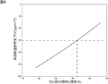
- FIG. 4 is a diagram showing the relationship between the normalized film thickness (%) of the SiO 2 film and the frequency temperature characteristics.
- FIG. 5 is a diagram showing the relationship between the normalized film thickness (%) of the SiO 2 film, the normalized film thickness (%) of the Mo layer in the IDT electrode, and the ratio band of the Sezawa wave.
- FIG. 1 is a circuit diagram of a band-pass filter according to the first embodiment.
- FIG. 2 is a schematic front cross-sectional view of the series arm resonator disposed closest to the antenna terminal in the first embodiment of the present invention.
- FIG. 3 is a schematic enlarged view of FIG.
- FIG. 4 is a diagram showing the relationship between the normal
- FIG. 6 is a diagram showing the relationship between the normalized film thickness (%) of the SiO 2 film and the normalized film thickness (%) of the Mo layer in the IDT electrode when the ratio band of the Sezawa wave is 0.1%. It is.
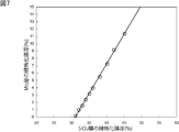
- FIG. 7 is a diagram showing the relationship between the normalized film thickness (%) of the SiO 2 film and the normalized film thickness (%) of the Mo layer in the IDT electrode when the ratio band of Sezawa waves is 0.05%. It is.
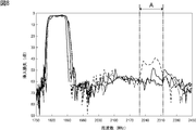
- FIG. 8 is a diagram showing attenuation frequency characteristics of the band-pass filter according to the present invention and the band-pass filter of the comparative example.
- FIG. 9 is a diagram showing the return loss at the antenna terminal of the band-pass filter according to the present invention and the band-pass filter of the comparative example.
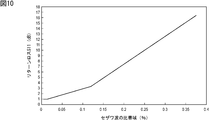
- FIG. 10 is a diagram showing the relationship between the ratio band of Sezawa waves and the return loss in region B in FIG.
- FIG. 11 is a schematic view of a composite filter device according to the second embodiment of the present invention.
- FIG. 12 is a schematic circuit diagram of a composite filter device according to the third embodiment of the present invention.
- FIG. 13 is a schematic circuit diagram of a band-pass filter according to the fourth embodiment of the present invention.
- FIG. 1 is a circuit diagram of a band-pass filter according to the first embodiment.
- the band-pass filter 1 is a ladder type filter having series arm resonators S1 to S6 and parallel arm resonators P1 to P3.
- Each of the plurality of series arm resonators S1 to S6 and the plurality of parallel arm resonators P1 to P3 includes an elastic wave resonator.
- the band-pass filter 1 has an input terminal 7 and an antenna terminal 6 connected to the antenna.
- the plurality of series arm resonators S1 to S6 are connected in series between the input terminal 7 and the antenna terminal 6.
- a parallel arm resonator P1 is connected between the connection point between the series arm resonator S1 and the series arm resonator S2 and the ground potential.
- a parallel arm resonator P2 is connected between a connection point between the series arm resonator S3 and the series arm resonator S4 and the ground potential.
- a parallel arm resonator P3 is connected between a connection point between the series arm resonator S5 and the series arm resonator S6 and the ground potential.
- the parallel arm resonators P2 and P3 are commonly connected to the ground potential.
- An impedance adjusting inductor L is connected between the antenna terminal 6 and the ground potential.
- the circuit configuration of the bandpass filter 1 is not particularly limited.
- the series arm resonators S1 to S6 and the parallel arm resonators P1 to P3 are elastic wave devices as an embodiment of the present invention having the following configuration. 2 and 3 below show the configuration of the series arm resonator S6.
- FIG. 2 is a schematic front cross-sectional view of the series arm resonator arranged closest to the antenna terminal in the first embodiment.
- FIG. 3 is a schematic enlarged view of FIG.
- the series arm resonator S ⁇ b> 6 has a LiNbO 3 substrate 2.
- the Euler angles ( ⁇ , ⁇ , ⁇ ) are Euler angles (0 °, 38 °, 0 °).
- the Euler angles ( ⁇ , ⁇ , ⁇ ) are Euler angles ( ⁇ 5 ° ⁇ ⁇ ⁇ 5 °, 28 ° ⁇ ⁇ ⁇ 48 °, ⁇ 5 ° ⁇ ⁇ ⁇ 5 °). Good.
- An IDT electrode 3 is provided on the LiNbO 3 substrate 2.
- the IDT electrode 3 has a plurality of electrode fingers 3a.
- Reflectors 8 are provided on both sides of the IDT electrode 3 in the elastic wave propagation direction.
- a series arm resonator S6 as an elastic wave resonator is formed. Note that the series arm resonators S1 to S5 and the parallel arm resonators P1 to P3 shown in FIG. 1 also have the same configuration as the series arm resonator S6.
- the band-pass filter 1 uses a Rayleigh wave that propagates through the LiNbO 3 substrate 2.
- the electrode finger 3 a of the IDT electrode 3 has a first electrode layer 3 a 1 laminated on the LiNbO 3 substrate 2.
- the first electrode layer 3a1 is a Mo layer containing Mo as a main component.
- Mo is the main component means that not only Mo but also an alloy containing 50% by weight or more of Mo is included.
- a second electrode layer 3a2 made of Al is laminated on the first electrode layer 3a1.
- the second electrode layer 3a2 may be made of a metal other than Al having a lower electrical resistance than Mo.
- the IDT electrode 3 may not have the second electrode layer 3a2. However, since the IDT electrode 3 includes the second electrode layer 3a2, the electric resistance of the IDT electrode 3 can be lowered.
- the first dielectric film 4 is provided on the LiNbO 3 substrate 2 so as to cover the IDT electrode 3.
- the first dielectric film 4 is a temperature characteristic compensation film.
- the band-pass filter 1 can improve the frequency temperature characteristic (TCV) by having the first dielectric film 4.
- the first dielectric film 4 is an SiO 2 film made of SiO 2.
- the first dielectric film 4 may be a dielectric film containing silicon oxide as a main component other than the SiO 2 film.
- the dielectric film containing silicon oxide as a main component means that it is not limited to SiO 2 but may be a film made of a dielectric material containing 50% by weight or more of SiO x (x is an integer).
- the second dielectric film 5 is provided on the first dielectric film 4.
- the second dielectric film 5 is a frequency adjustment film.
- the second dielectric film 5 is made of SiN.
- the band pass filter 1 can adjust the frequency by adjusting the thickness of the second dielectric film 5.
- the second dielectric film 5 may be made of an appropriate dielectric other than SiN. Further, the second dielectric film 5 may not be provided.
- the film thickness of the first dielectric film 4 refers to the surface of the first dielectric film 4 in contact with the LiNbO 3 substrate 2 and the upper surface of the first dielectric film 4, that is, the second dielectric film. The distance to the surface in contact with 5 shall be said.
- the film thickness normalized by the wavelength defined by the electrode finger pitch of the IDT electrode 3 is defined as a normalized film thickness (%).
- Normalized thickness of the first electrode layer 3a1 shown in Figure 3 (%) and T 1 the first dielectric film 4 of a normalized film thickness (%) of the T 2.
- the first electrode layer 3a1 is mainly composed of Mo, T 2 ⁇ 31%, and satisfies the following formula (1).
- FIG. 4 is a diagram showing the relationship between the normalized film thickness (%) of the SiO 2 film and the frequency temperature characteristics. Note that the normalized film thickness (%) of the SiO 2 film in FIG. 4 corresponds to the normalized film thickness (%) T 2 of the first dielectric film in the present embodiment.
- the value of the frequency temperature characteristic is ⁇ 30 ppm / ° C. or more. It becomes.
- the frequency temperature characteristic value is ⁇ 30 ppm / ° C. or less.
- the present inventors have found that the higher-order mode depends not only on the thickness of the first dielectric film but also on the thickness of the first electrode layer that is Mo in the IDT electrode.
- the normalized film thickness (%) T 2 of the first dielectric film is set to a size that can effectively improve the frequency temperature characteristics, and further, the higher-order mode can be suppressed by satisfying the above formula (1). I found out that I could do it. This will be described using the Sezawa wave, which is a higher-order mode of the Rayleigh wave, as an example.
- the frequency of the Sezawa wave is a frequency that maximizes the return loss on the input terminal side of the bandpass filter.
- FIG. 5 is a diagram showing the relationship between the normalized film thickness (%) of the SiO 2 film, the normalized film thickness (%) of the Mo layer in the IDT electrode, and the ratio band of the Sezawa wave. Note that the normalized film thickness (%) of the SiO 2 film in FIG. 5 and FIGS. 6 and 7 described later corresponds to the normalized film thickness (%) T 2 of the first dielectric film in the present embodiment. The normalized film thickness (%) of the Mo layer corresponds to the normalized film thickness (%) T 1 of the first electrode layer in the IDT electrode.
- FIG. 6 is a diagram showing the relationship between the normalized film thickness (%) of the SiO 2 film and the normalized film thickness (%) of the Mo layer in the IDT electrode when the ratio band of the Sezawa wave is 0.1%. It is.
- FIG. 7 is a diagram showing the relationship between the normalized film thickness (%) of the SiO 2 film and the normalized film thickness (%) of the Mo layer in the IDT electrode when the ratio band of Sezawa waves is 0.05%. It is.
- the specific bandwidth of the Sezawa wave can be reduced to 0.05% or less.
- the antenna terminal may be used as an antenna common terminal, and a plurality of other filters may be connected to the antenna common terminal. At this time, the influence of the bandpass filter of the present embodiment on the passband of the other filter can be reduced by setting the specific band of the Sezawa wave to 0.05% or less. This will be described below.
- band-pass filters having a specific band of Sezawa waves of 0.098%, 0.012%, and 0.005% were produced.
- a bandpass filter of the comparative example a bandpass filter having a Sezawa wave specific band of 0.3% was manufactured. The attenuation frequency characteristics and return loss of each of the bandpass filters were compared.
- FIG. 8 is a diagram showing attenuation frequency characteristics of the band-pass filter according to the present invention and the band-pass filter of the comparative example.
- FIG. 9 is a diagram illustrating the return loss at the antenna terminal of the band-pass filter according to the present invention and the band-pass filter of the comparative example. 8 and 9, the solid line indicates the result of the specific bandwidth of 0.098%. The alternate long and short dash line indicates the result with a specific band of 0.012%. The alternate long and two short dashes line indicates the result of a specific band of 0.005%. A broken line shows the result of a relative bandwidth of 0.3% as a comparative example.
- spurious due to the Sezawa wave is generated in the region A, but it can be seen that the spurious is remarkably suppressed in the filter having a Sezawa wave specific band of 0.098% or less.
- the return loss has a relative bandwidth of Sezawa waves of 0.012% or less, which indicates that the return loss is remarkably suppressed.
- FIG. 10 is a diagram showing the relationship between the ratio band of Sezawa waves and the return loss in the region B in FIG.
- the ratio band of the Sezawa wave is 0.1% or less
- the attenuation characteristic in the region B can be effectively reduced and the Sezawa wave can be suppressed.
- the Sezawa wave can be reduced to 0.1% or less.
- At least one of the series arm resonators S1 to S6 and the parallel arm resonators P1 to P3 may be composed of an elastic wave device having the above-described configuration shown in FIGS.
- at least one of the series arm resonators S1 to S6 is made of an elastic wave device having the above-described configuration.
- the series arm resonator S6 closest to the antenna terminal 6 is an elastic wave resonator having the above-described configuration. Thereby, Sezawa waves can be further suppressed.
- the film thickness of the first electrode layer 3a1 of the IDT electrode 3 shown in FIG. 3 is preferably 600 nm or less.
- the normalized film thickness (%) T 1 of the first electrode layer 3a1 is preferably T 1 ⁇ 15%.
- the first electrode layer 3a1 can be provided by, for example, a sputtering method. At this time, the stress applied to the LiNbO 3 substrate 2 increases as the thickness of the first electrode layer 3a1 increases. By setting the film thickness or normalized film thickness (%) T 1 of the first electrode layer 3a1 within the above range, the LiNbO 3 substrate 2 is hardly damaged.
- FIG. 11 is a schematic diagram of a composite filter device according to the second embodiment of the present invention.
- the composite filter device 10 is used in a carrier aggregation system.
- the composite filter device 10 has an antenna common terminal 16 connected to the antenna.
- the composite filter device 10 includes first to third band-pass filters 11 a to 11 c that are commonly connected to the antenna common terminal 16.
- the first to third band-pass filters 11a to 11c are provided to support a plurality of carriers, that is, communication methods.
- the first, second, and third band-pass filters 11a, 11b, and 11c are reception filters.
- the combination of the transmission filter and the reception filter is not limited to the above.
- the first band-pass filter 11a has the same configuration as that of the first embodiment.
- the first band-pass filter 11a is a band-pass filter having a return loss when the ratio band of the Sezawa wave in FIG. 9 is 0.098%.
- the pass band of the second band pass filter 11b is located within the region B in FIG. Note that the pass band of the second band pass filter 11b is not particularly limited as long as it is located higher than the pass band of the first band pass filter 11a.
- the higher-order mode can be suppressed as described above. Therefore, in the second band pass filter 11b, it is difficult to cause an influence due to the response of the higher order mode.
- the pass band of the first band-pass filter 11a is located on the lower band side of the pass band of the second band-pass filter 11b. Therefore, even if a higher-order mode is generated in the second band-pass filter 11b, the first band-pass filter 11a is hardly affected by the response of the higher-order mode.
- the pass band of the third band pass filter 11c is not particularly limited, but is preferably located on the higher frequency side than the pass band of the first band pass filter 11a. Thereby, similarly to the second band-pass filter 11b, it is difficult to produce an influence due to the response of the higher-order mode.
- composite filter device 10 does not have to include the third band-pass filter 11c.
- the first band-pass filter 11a and the second band-pass filter 11b may be formed on the same piezoelectric substrate.
- the present invention can also be suitably applied to a composite filter device having four or more band-pass filters and a duplexer.
- FIG. 12 is a schematic circuit diagram of a composite filter device according to the third embodiment of the present invention.
- the composite filter device 20 can also be used in a carrier aggregation system.
- This composite filter device 20 has an antenna common terminal 26 as a common terminal.
- a plurality of duplexers 21A to 21E are connected to the antenna common terminal.
- the duplexers 21A to 21E have transmission filters 21Aa to 21Ea and reception filters 21Ab to 21Eb, respectively.
- any one of the transmission filters 21Aa to 21Ea is a first bandpass filter according to the present invention, and at least one of the remaining transmission filters or reception filters is the second bandpass filter of the present invention.
- a band pass filter may be used. That is, one of the plurality of bandpass filters connected to the antenna common terminal 26 which is a common terminal is set as a first bandpass filter, and at least one of the other bandpass filters is set as the first bandpass filter. Two band-pass filters may be used. Thereby, the response due to the Sezawa wave in the first band pass filter can be suppressed, and the influence of the response due to the Sezawa wave also in the second band pass filter commonly connected to the first band pass filter. Can be effectively suppressed.
- a duplexer having a first bandpass filter may have a longitudinally coupled resonator type acoustic wave filter that is connected to the antenna common terminal 26 in common with the first bandpass filter.
- FIG. 13 is a schematic circuit diagram of a band-pass filter according to the fourth embodiment.
- the band-pass filter 30 has a longitudinally coupled resonator type elastic wave filter 31 a connected to the antenna common terminal 36.
- a ladder type filter 31b is connected between the longitudinally coupled resonator type elastic wave filter 31a and the antenna common terminal.
- the ladder filter 31b includes series arm resonators S31 and S32 and parallel arm resonators P31 and P32.
- the longitudinal band resonator type elastic wave filter 31a and the ladder type filter 31b constitute a pass band.
- An inductor L for adjusting impedance is connected between the antenna common terminal 36 and the ground potential.
- the circuit configuration of the band pass filter 30 is not particularly limited.
- the feature of this embodiment is that at least one of the series arm resonators S31 and S32, the parallel arm resonators P31 and P32, and the longitudinally coupled resonator type acoustic wave filter 31a has the above-described configuration shown in FIGS. It consists of the elastic wave resonator which has.
- at least one of the series arm resonators S32 to S31 is composed of an acoustic wave resonator having the above-described configuration. Thereby, Sezawa waves can be effectively suppressed.
- the series arm resonator S32 closest to the antenna common terminal 36 is an elastic wave resonator having the above-described configuration. Thereby, Sezawa waves can be further suppressed.
- the first electrode layer containing Mo as a main component is preferably an alloy containing Nb.
- TCF can be further improved.
- the specific form of the composite filter device is not particularly limited as long as the composite filter device of the present invention includes the first and second band-pass filters connected to the antenna common terminal. Therefore, according to the present invention, a duplexer, a multiplexer, a high-frequency front-end circuit of a communication device, a high-frequency front-end module, a communication device such as a mobile phone, and the like including the above composite filter device are provided.
Landscapes
- Physics & Mathematics (AREA)
- Acoustics & Sound (AREA)
- Surface Acoustic Wave Elements And Circuit Networks Thereof (AREA)
Abstract
LiNbO3基板を伝搬するレイリー波を利用する場合においても、周波数温度特性を効果的に改善することができ、かつ高次モードを抑制することができる、弾性波装置を提供する。 直列腕共振子S6(弾性波装置)は、オイラー角(φ,θ,ψ)がオイラー角(-5°≦φ≦5°,28°≦θ≦48°,-5°≦ψ≦5°)であるLiNbO3基板2と、LiNbO3基板2上に設けられており、Moを主成分とする第1の電極層3a1を有し、かつ複数本の電極指3aを有するIDT電極3と、LiNbO3基板2上に、IDT電極3を覆っている第1の誘電体膜4とを備える。IDT電極3の電極指ピッチにより規定される波長により規格化された膜厚を規格化膜厚(%)とし、第1の電極層3a1の規格化膜厚(%)をT1、第1の誘電体膜4の規格化膜厚(%)をT2としたときに、T2≧31%であり、かつ式(1)…T1≧0.8634×T2-27.913を満たす。
Description
本発明は、弾性波装置、帯域通過型フィルタ及びこれらを用いた複合フィルタ装置に関する。
下記の特許文献1においては、レイリー波を利用している帯域通過型フィルタが開示されている。この帯域通過型フィルタは、LiNbO3基板上に形成されたIDT電極が、酸化ケイ素膜に覆われた構成を有する。レイリー波の高次モードを抑制するために、酸化ケイ素膜の膜厚が薄くされている。そして、IDT電極はCu(銅)を主成分とする。
特許文献1の構成のように、LiNbO3基板を伝搬するレイリー波を利用し、かつ、Cuを主成分としたIDT電極を用いる場合、Cuの膜厚は高次モードには影響せず、酸化ケイ素膜の膜厚のみ高次モードに影響する。
そのため、酸化ケイ素膜の膜厚を厚くすれば、周波数温度特性は向上するが、高次モードが発生してしまう。また、酸化ケイ素膜の膜厚を薄くすれば、周波数温度特性は低下するが、高次モードは抑制される。
そのため、LiNbO3基板を伝搬するレイリー波を利用し、かつ、Cuを主成分としたIDT電極を用いる場合には、上記高次モードの抑制と周波数温度特性の改善とを両立することは困難であった。
本発明の目的は、LiNbO3基板を伝搬するレイリー波を利用する場合においても、周波数温度特性を効果的に改善することができ、かつ高次モードを抑制することができる、弾性波装置及び帯域通過型フィルタを提供することにある。また、本発明の他の目的は、高次モードの応答による影響が生じ難い、複合フィルタ装置を提供することにある。
本発明は、上記高次モードが酸化ケイ素膜の膜厚だけではなく、IDT電極におけるMo(モリブデン)膜の膜厚にも依存することを、本願発明者らが見出したことに基づくものである。
本発明に係る弾性波装置は、オイラー角(φ,θ,ψ)がオイラー角(-5°≦φ≦5°,28°≦θ≦48°,-5°≦ψ≦5°)であるLiNbO3基板と、前記LiNbO3基板上に設けられており、Moを主成分とする第1の電極層を有し、かつ複数本の電極指を有するIDT電極と、前記LiNbO3基板上に、前記IDT電極を覆っている第1の誘電体膜とを備え、前記LiNbO3基板を伝搬するレイリー波を利用しており、前記IDT電極の電極指ピッチにより規定される波長により規格化された膜厚を規格化膜厚(%)とし、前記第1の電極層の規格化膜厚(%)をT1、前記第1の誘電体膜の規格化膜厚(%)をT2としたときに、T2≧31%であり、かつ下記の式(1)
式(1)
T1≧0.8634×T2-27.913
を満たす。
式(1)
T1≧0.8634×T2-27.913
を満たす。
本発明に係る弾性波装置のある特定の局面では、下記の式(2)
式(2)
T1≧0.8106×T2-25.089
が満たされている。この場合には、高次モードをより一層抑制することができる。
式(2)
T1≧0.8106×T2-25.089
が満たされている。この場合には、高次モードをより一層抑制することができる。
本発明に係る弾性波装置の他の特定の局面では、T1≦15%である。この場合には、LiNbO3基板が破損し難い。
本発明に係る弾性波装置のさらに他の特定の局面では、前記第1の誘電体膜が酸化ケイ素を主成分とする。この場合には、周波数温度特性をより一層改善することができる。
本発明に係る弾性波装置の別の特定の局面では、前記第1の誘電体膜がSiO2からなる。この場合には、周波数温度特性をより一層改善することができる。
本発明に係る弾性波装置のさらに別の特定の局面では、前記第1の誘電体膜上に、第2の誘電体膜が積層されている。この場合には、周波数の調整などを行うことができる。
本発明に係る弾性波装置のさらに別の特定の局面では、前記第2の誘電体膜がSiNからなる。この場合には、周波数を調整することができる。
本発明に係る弾性波装置のさらに別の特定の局面では、前記IDT電極において、前記第1の電極層上に、Moよりも電気抵抗が低い金属からなる第2の電極層が積層されている。この場合には、IDT電極の電気抵抗を低くすることができる。
本発明に係る弾性波装置のさらに別の特定の局面では、前記第2の電極層が、Alからなる。この場合には、IDT電極の電気抵抗を低くすることができる。
本発明に係る弾性波装置のさらに他の特定の局面では、前記Moを主成分とする第1の電極層はNbを含む合金である。
本発明に係る帯域通過型フィルタは、アンテナに接続されるアンテナ端子と、前記アンテナ端子に接続されている、本発明に従って構成された弾性波装置とを備える。
本発明に係る帯域通過型フィルタのある特定の局面では、直列腕共振子及び並列腕共振子を有するラダー型フィルタであり、前記直列腕共振子及び前記並列腕共振子のうちの少なくとも1つが前記弾性波装置からなる。
本発明に係る帯域通過型フィルタの他の特定の局面では、前記直列腕共振子を複数有し、前記複数の直列腕共振子のうちの少なくとも1つが前記弾性波装置からなる。この場合には、高次モードを効果的に抑制することができる。
本発明に係る帯域通過型フィルタのさらに他の特定の局面では、前記複数の直列腕共振子のうち、前記アンテナ端子に最も近い直列腕共振子が前記弾性波装置からなる。この場合には、高次モードをより一層抑制することができる。
本発明に係る帯域通過型フィルタの他の特定の局面では、前記ラダー型フィルタに接続されている縦結合共振子型弾性波フィルタをさらに有する。
本発明に係る帯域通過型フィルタのさらに他の特定の局面では、前記縦結合共振子型弾性波フィルタが、前記ラダー型フィルタの前記アンテナ端子とは逆の側に接続されている。
本発明に係る帯域通過型フィルタの別の特定の局面では、前記弾性波装置としての縦結合共振子型弾性波フィルタを有する。
本発明に係る複合フィルタ装置は、本発明に従って構成された帯域通過型フィルタからなる、第1の帯域通過型フィルタと、前記アンテナ端子に接続されており、前記第1の帯域通過型フィルタの通過帯域よりも高域側に通過帯域を有する少なくとも1つの第2の帯域通過型フィルタとを備える。
前記複合フィルタ装置のさらに他の特定の局面では、本発明に従って構成された帯域通過型フィルタからなる、第1の帯域通過型フィルタと、前記アンテナ端子に接続されており、前記第1の帯域通過型フィルタの通過帯域よりも高域側に通過帯域を有する少なくとも1つの第2の帯域通過型フィルタとが、同一の圧電基板上に形成されている。
本発明に係る複合フィルタ装置のある特定の局面では、前記第1の帯域通過型フィルタを含むデュプレクサを有し、該デュプレクサが、前記アンテナ端子に前記第1の帯域通過型フィルタと共通接続されている、縦結合共振子型弾性波フィルタを有する。
本発明に係る弾性波装置及び帯域通過型フィルタによれば、LiNbO3基板を伝搬するレイリー波を利用する場合においても、周波数温度特性を効果的に改善することができ、かつ高次モードを抑制することができる。また、本発明に係る複合フィルタ装置によれば、高次モードの応答による影響が生じ難い。
以下、図面を参照しつつ、本発明の具体的な実施形態を説明することにより、本発明を明らかにする。
なお、本明細書に記載の各実施形態は、例示的なものであり、異なる実施形態間において、構成の部分的な置換または組み合わせが可能であることを指摘しておく。
図1は、第1の実施形態に係る帯域通過型フィルタの回路図である。
図1に示すように、帯域通過型フィルタ1は、直列腕共振子S1~S6及び並列腕共振子P1~P3を有するラダー型フィルタである。複数の直列腕共振子S1~S6及び複数の並列腕共振子P1~P3は、いずれも、弾性波共振子からなる。
帯域通過型フィルタ1は、入力端子7と、アンテナに接続されるアンテナ端子6とを有する。複数の直列腕共振子S1~S6は、入力端子7とアンテナ端子6との間に互いに直列に接続されている。
直列腕共振子S1と直列腕共振子S2との間の接続点とグラウンド電位との間には、並列腕共振子P1が接続されている。直列腕共振子S3と直列腕共振子S4との間の接続点とグラウンド電位との間には、並列腕共振子P2が接続されている。直列腕共振子S5と直列腕共振子S6との間の接続点とグラウンド電位との間には、並列腕共振子P3が接続されている。なお、並列腕共振子P2,P3は、グラウンド電位に共通接続されている。アンテナ端子6とグラウンド電位との間には、インピーダンス調整用のインダクタLが接続されている。なお、帯域通過型フィルタ1の回路構成は、特に限定されない。
直列腕共振子S1~S6及び並列腕共振子P1~P3は、以下に述べる構成を有する本発明の一実施形態としての弾性波装置である。なお、下記の図2及び図3は、直列腕共振子S6の構成を示す。
図2は、第1の実施形態における、最もアンテナ端子側に配置された直列腕共振子の模式的正面断面図である。図3は、図2の模式的拡大図である。
図2に示すように、直列腕共振子S6は、LiNbO3基板2を有する。本実施形態においては、LiNbO3基板2は、オイラー角(φ,θ,ψ)がオイラー角(0°,38°,0°)である。なお、LiNbO3基板2は、オイラー角(φ,θ,ψ)がオイラー角(-5°≦φ≦5°,28°≦θ≦48°,-5°≦ψ≦5°)であればよい。
LiNbO3基板2上には、IDT電極3が設けられている。IDT電極3は、複数本の電極指3aを有する。IDT電極3に交流電圧を印加することにより、弾性波が励振される。IDT電極3の弾性波伝搬方向両側には、反射器8が設けられている。それによって、弾性波共振子としての直列腕共振子S6が構成されている。なお、図1に示す直列腕共振子S1~S5及び並列腕共振子P1~P3も、直列腕共振子S6と同様の構成を有する。
本実施形態では、帯域通過型フィルタ1は、LiNbO3基板2を伝搬するレイリー波を利用している。
図3に示すように、IDT電極3の電極指3aは、LiNbO3基板2上に積層されている第1の電極層3a1を有する。第1の電極層3a1はMoを主成分とするMo層である。なお、Moを主成分とするとは、Moのみからなるものに限らず、Moを50重量%以上含む合金をも含むことを意味する。
第1の電極層3a1上には、Alからなる第2の電極層3a2が積層されている。なお、第2の電極層3a2は、Moよりも電気抵抗が低い、Al以外の金属からなっていてもよい。あるいは、IDT電極3は、第2の電極層3a2を有しなくともよい。もっとも、IDT電極3が第2の電極層3a2を有することにより、IDT電極3の電気抵抗を低くすることができる。
図2に戻り、LiNbO3基板2上には、IDT電極3を覆うように、第1の誘電体膜4が設けられている。第1の誘電体膜4は、温度特性補償膜である。帯域通過型フィルタ1は、第1の誘電体膜4を有することにより、周波数温度特性(TCV)を改善することができる。
本実施形態においては、第1の誘電体膜4は、SiO2からなるSiO2膜である。なお、第1の誘電体膜4には、SiO2膜以外の、酸化ケイ素を主成分とする誘電体膜を用いることもできる。酸化ケイ素を主成分とする誘電体膜とは、SiO2に限らず、SiOx(xは整数)を50重量%以上含む誘電体材料からなる膜であってもよいことを意味する。
第1の誘電体膜4上には、第2の誘電体膜5が設けられている。第2の誘電体膜5は周波数調整膜である。第2の誘電体膜5は、SiNからなる。帯域通過型フィルタ1は、第2の誘電体膜5の膜厚を調整することにより、周波数を調整することができる。なお、第2の誘電体膜5は、SiN以外の適宜の誘電体からなっていてもよい。また、第2の誘電体膜5は、設けられていなくともよい。
なお、第1の誘電体膜4の膜厚とは、第1の誘電体膜4のLiNbO3基板2と接している面と、第1の誘電体膜4の上面すなわち第2の誘電体膜5と接している面までの距離を言うものとする。
ここで、IDT電極3の電極指ピッチにより規定される波長により規格化された膜厚を規格化膜厚(%)とする。図3に示した第1の電極層3a1の規格化膜厚(%)をT1とし、第1の誘電体膜4の規格化膜厚(%)をT2とする。
本実施形態の特徴は、第1の電極層3a1がMoを主成分とし、T2≧31%であり、かつ下記の式(1)を満たすことにある。
式(1)
T1≧0.8634×T2-27.913
T1≧0.8634×T2-27.913
それによって、周波数温度特性を効果的に改善することができ、かつ高次モードを抑制することができる。これを以下において説明する。
図4は、SiO2膜の規格化膜厚(%)と周波数温度特性との関係を示す図である。なお、図4におけるSiO2膜の規格化膜厚(%)は、本実施形態における第1の誘電体膜の規格化膜厚(%)T2に相当する。
図4に示すように、SiO2膜の規格化膜厚(%)が大きいほど、周波数温度特性の値が大きくなっていることがわかる。本実施形態においては、図4中の破線で示すように、第1の誘電体膜の規格化膜厚(%)T2が31%以上になると、周波数温度特性の値が-30ppm/℃以上となる。そして、圧電基板にLiTaO3を用い、該圧電基板上にAlからなるIDT電極を形成した一般的な弾性表面波素子では、周波数温度特性の値が-30ppm/℃以下であるため、第1の誘電体膜の規格化膜厚(%)T2が31%以上になると、一般的な弾性表面波素子以上に、周波数温度特性を改善することができる。
ここで、本願発明者らは、高次モードは第1の誘電体膜の膜厚だけではなく、IDT電極における、Moである第1の電極層の膜厚にも依存することを見出した。第1の誘電体膜の規格化膜厚(%)T2を、周波数温度特性を効果的に改善し得る大きさとし、さらに、上記式(1)を満たすことにより、高次モードの抑制をも果たし得ることを見出した。これを、レイリー波の高次モードであるセザワ波を例として説明する。
なお、セザワ波が複数のレスポンスを有する場合、あるいは帯域を持って生じた場合には、セザワ波の周波数は、帯域通過型フィルタの入力端子側のリターンロスが最大になる周波数とする。
図5は、SiO2膜の規格化膜厚(%)及びIDT電極におけるMo層の規格化膜厚(%)と、セザワ波の比帯域との関係を示す図である。なお、図5並びに後述する図6及び図7におけるSiO2膜の規格化膜厚(%)は、本実施形態における第1の誘電体膜の規格化膜厚(%)T2に相当する。Mo層の規格化膜厚(%)は、IDT電極における第1の電極層の規格化膜厚(%)T1に相当する。
図5に示すように、SiO2膜の規格化膜厚(%)が大きいほど、セザワ波の比帯域が大きくなっていることがわかる。他方、Mo層の規格化膜厚(%)が大きいほど、セザワ波の比帯域が小さくなっていることがわかる。このように、SiO2膜の規格化膜厚(%)を大きくしても、Mo層の規格化膜厚(%)を大きくすることにより、セザワ波の比帯域を小さくすることができる。
ここで、セザワ波の比帯域が0.1%以下、及び0.05%以下となる条件をそれぞれ求めた。
図6は、セザワ波の比帯域が0.1%になるときの、SiO2膜の規格化膜厚(%)とIDT電極におけるMo層の規格化膜厚(%)との関係を示す図である。図7は、セザワ波の比帯域が0.05%になるときの、SiO2膜の規格化膜厚(%)とIDT電極におけるMo層の規格化膜厚(%)との関係を示す図である。
上記の式(1)は、図6に示す関係から導き出される。式(1)を満たすことにより、セザワ波の比帯域を0.1%以下とすることができ、セザワ波を抑制することができる。
図7に示すように、下記の式(2)を満たすことにより、セザワ波の比帯域を0.05%以下にすることができる。
式(2)
T1≧0.8106×T2-25.089
T1≧0.8106×T2-25.089
セザワ波の比帯域を小さくするほど、セザワ波をより一層抑制することができる。セザワ波の比帯域を0.1%以下とすることにより、帯域通過型フィルタの減衰特性を改善することができる。ここで、アンテナ端子をアンテナ共通端子として、該アンテナ共通端子に他の複数のフィルタを接続してもよい。このとき、セザワ波の比帯域を0.05%以下とすることで、本実施形態の帯域通過型フィルタによる、上記他のフィルタの通過帯域への影響を小さくすることができる。これを以下において説明する。
本発明の構成を有する帯域通過型フィルタとして、セザワ波の比帯域が0.098%、0.012%及び0.005%である帯域通過型フィルタをそれぞれ作製した。比較例の帯域通過型フィルタとして、セザワ波の比帯域が0.3%である帯域通過型フィルタを作製した。上記各帯域通過型フィルタの減衰量周波数特性及びリターンロスを比較した。
図8は、本発明に係る帯域通過型フィルタ及び比較例の帯域通過型フィルタの減衰量周波数特性を示す図である。図9は、本発明に係る帯域通過型フィルタ及び比較例の帯域通過型フィルタの、アンテナ端子におけるリターンロスを示す図である。図8及び図9において、実線は比帯域0.098%の結果を示す。一点鎖線は比帯域0.012%の結果を示す。二点鎖線は比帯域0.005%の結果を示す。破線は比較例である比帯域0.3%の結果を示す。
図8に示すように、領域Aにはセザワ波によるスプリアスが生じているが、セザワ波の比帯域が0.098%以下のフィルタにおいては、そのスプリアスが著しく抑制されていることがわかる。
また、図9に示すように、リターンロスはセザワ波の比帯域が0.012%以下となっており、著しく抑制されていることがわかる。
図10は、セザワ波の比帯域と、図9中の領域Bにおけるリターンロスとの関係を示す図である。
図10に示すように、セザワ波の比帯域が0.1%以下において、領域Bにおける減衰特性を効果的に小さくすることができ、セザワ波を抑制し得ることがわかる。上述したように、上記式(1)を満たすことにより、セザワ波を0.1%以下とすることができる。
より好ましくは、上記の式(2)を満たすことが望ましい。それによって、セザワ波をより一層抑制することができ、アンテナ共通端子において他の通過帯域などを有するフィルタと接続したときの、他のフィルタへの影響を小さくし得る。
なお、直列腕共振子S1~S6及び並列腕共振子P1~P3のうちの少なくとも1つが、図2及び図3に示した上記構成を有する弾性波装置からなっていればよい。好ましくは、直列腕共振子S1~S6のうちの少なくとも1つが、上記構成を有する弾性波装置からなることが望ましい。それによって、セザワ波を効果的に抑制することができる。
より好ましくは、アンテナ端子6に最も近い直列腕共振子S6が上記構成を有する弾性波共振子からなることが望ましい。それによって、セザワ波をより一層抑制することができる。
ところで、図3に示したIDT電極3の第1の電極層3a1の膜厚は、600nm以下とすることが好ましい。あるいは、第1の電極層3a1の規格化膜厚(%)T1は、T1≦15%であることが好ましい。第1の電極層3a1は、例えば、スパッタリング法により設けることができる。このとき、第1の電極層3a1の膜厚が厚くなるほど、LiNbO3基板2に加わる応力が大きくなる。第1の電極層3a1の膜厚または規格化膜厚(%)T1を上記の範囲内とすることにより、LiNbO3基板2が破損し難い。
図11は、本発明の第2の実施形態に係る複合フィルタ装置の模式図である。
複合フィルタ装置10は、キャリアアグリゲーションシステムに用いられるものである。複合フィルタ装置10は、アンテナに接続されるアンテナ共通端子16を有する。複合フィルタ装置10は、アンテナ共通端子16に共通接続されている第1~第3の帯域通過型フィルタ11a~11cを有する。第1~第3の帯域通過型フィルタ11a~11cは、複数のキャリア、すなわち通信方式に対応するために設けられている。
本実施形態では、第1、第2,第3の帯域通過型フィルタ11a、11b,11cは受信フィルタである。なお、複合フィルタ装置10において、送信フィルタ及び受信フィルタの組み合わせは、上記に限定されない。
第1の帯域通過型フィルタ11aは、第1の実施形態と同様の構成を有する。本実施形態においては、第1の帯域通過型フィルタ11aは、図9における、セザワ波の比帯域が0.098%の場合のリターンロスを有する帯域通過型フィルタである。
第2の帯域通過型フィルタ11bの通過帯域は、図9における領域Bの範囲内に位置する。なお、第2の帯域通過型フィルタ11bの通過帯域は、特に限定されず、第1の帯域通過型フィルタ11aの通過帯域よりも高域側に位置していればよい。
第1の帯域通過型フィルタ11aにおいては、上述したように、高次モードを抑制することができる。よって、第2の帯域通過型フィルタ11bにおいて、高次モードの応答による影響が生じ難い。
加えて、第1の帯域通過型フィルタ11aの通過帯域は第2の帯域通過型フィルタ11bの通過帯域の低域側に位置する。よって、第2の帯域通過型フィルタ11bにおいて高次モードが発生していたとしても、第1の帯域通過型フィルタ11aにおいて、高次モードの応答による影響が生じ難い。
第3の帯域通過型フィルタ11cの通過帯域は、特に限定されないが、第1の帯域通過型フィルタ11aの通過帯域よりも高域側に位置することが好ましい。それによって、第2の帯域通過型フィルタ11bと同様に、高次モードの応答による影響が生じ難い。
なお、複合フィルタ装置10は、第3の帯域通過型フィルタ11cを有していなくともよい。
なお、複合フィルタ装置10は、第1の帯域通過型フィルタ11aと第2の帯域通過型フィルタ11bとが同一の圧電基板上に形成されていても良い。
本発明は、4つ以上の帯域通過型フィルタや、デュプレクサなどを有する複合フィルタ装置においても、好適に適用することができる。
図12は、本発明の第3の実施形態に係る複合フィルタ装置の略図的回路図である。複合フィルタ装置20は、キャリアアグリゲーションシステムに用いることもできる。この複合フィルタ装置20は、共通端子としてのアンテナ共通端子26を有する。アンテナ共通端子26に、複数のデュプレクサ21A~21Eが接続されている。
各デュプレクサ21A~21Eは、それぞれ、送信フィルタ21Aa~21Eaと、受信フィルタ21Ab~21Ebとを有する。このような複合フィルタ装置20においても、いずれかの送信フィルタ21Aa~21Eaを本発明に従って、第1の帯域通過型フィルタとし、残りの送信フィルタまたは受信フィルタのうち少なくとも1つを本発明の第2の帯域通過型フィルタとしてもよい。すなわち、共通端子であるアンテナ共通端子26に接続されている複数の帯域通過型フィルタのいずれか1つを第1の帯域通過型フィルタとし、他の帯域通過型フィルタのうちの少なくとも1つを第2の帯域通過型フィルタとしてもよい。それによって第1の帯域通過型フィルタにおけるセザワ波による応答を抑制することができ、第1の帯域通過型フィルタと共通接続している第2の帯域通過型フィルタにおいても、セザワ波による応答の影響を効果的に抑制することができる。
例えば、第1の帯域通過型フィルタを有するデュプレクサは、アンテナ共通端子26に第1の帯域通過型フィルタと共通接続されている、縦結合共振子型弾性波フィルタを有していてもよい。
図13は、第4の実施形態に係る帯域通過型フィルタの略図的回路図である。本実施形態では、帯域通過型フィルタ30は、アンテナ共通端子36に縦結合共振子型弾性波フィルタ31aが接続されている。縦結合共振子型弾性波フィルタ31aとアンテナ共通端子36との間に、ラダー型フィルタ31bが接続されている。ラダー型フィルタ31bは、直列腕共振子S31,S32と並列腕共振子P31、P32とを有する。帯域通過型フィルタ30では、縦結合共振子型弾性波フィルタ31aと、ラダー型フィルタ31bとにより通過帯域が構成されている。アンテナ共通端子36とグラウンド電位との間には、インピーダンス調整用のインダクタLが接続されている。なお、帯域通過型フィルタ30の回路構成は、特に限定されない。
本実施形態の特徴は、直列腕共振子S31,S32及び並列腕共振子P31,P32及び縦結合共振子型弾性波フィルタ31aのうちの少なくとも1つが、図2及び図3に示した上記構成を有する弾性波共振子からなっていることを特徴とする。好ましくは、直列腕共振子S32~S31のうちの少なくとも1つが、上記構成を有する弾性波共振子からなることが望ましい。それによって、セザワ波を効果的に抑制することができる。
より好ましくは、アンテナ共通端子36に最も近い直列腕共振子S32が上記構成を有する弾性波共振子からなることが望ましい。それによって、セザワ波をより一層抑制することができる。
より好ましくは、前記Moを主成分とする第1の電極層は、Nbを含む合金であることが望ましい。それによって、TCFをより一層改善することができる。
なお、本発明の複合フィルタ装置は、アンテナ共通端子に接続される第1,第2の帯域通過型フィルタを備える限り、その複合フィルタ装置の具体的な形態は特に限定されない。従って、本発明によれば、上記複合フィルタ装置を含む、デュプレクサ、マルチプレクサ、通信装置の高周波フロントエンド回路や高周波フロントエンドモジュールや携帯電話機のような通信装置等が提供される。
1…帯域通過型フィルタ
2…LiNbO3基板
3…IDT電極
3a…電極指
3a1,3a2…第1,第2の電極層
4,5…第1,第2の誘電体膜
6…アンテナ端子
7…入力端子
8…反射器
10…複合フィルタ装置
11a~11c…第1~第3の帯域通過型フィルタ
16…アンテナ共通端子
20…複合フィルタ装置
21A~21E…デュプレクサ
21Aa~21Ea…送信フィルタ
21Ab~21Eb…受信フィルタ
26…アンテナ共通端子
30…帯域通過型フィルタ
31a…縦結合共振子型弾性波フィルタ
31b…ラダー型フィルタ
36…アンテナ共通端子
S1~S6、S31、S32…直列腕共振子
P1~P3、P31、P32…並列腕共振子
L…インダクタ
2…LiNbO3基板
3…IDT電極
3a…電極指
3a1,3a2…第1,第2の電極層
4,5…第1,第2の誘電体膜
6…アンテナ端子
7…入力端子
8…反射器
10…複合フィルタ装置
11a~11c…第1~第3の帯域通過型フィルタ
16…アンテナ共通端子
20…複合フィルタ装置
21A~21E…デュプレクサ
21Aa~21Ea…送信フィルタ
21Ab~21Eb…受信フィルタ
26…アンテナ共通端子
30…帯域通過型フィルタ
31a…縦結合共振子型弾性波フィルタ
31b…ラダー型フィルタ
36…アンテナ共通端子
S1~S6、S31、S32…直列腕共振子
P1~P3、P31、P32…並列腕共振子
L…インダクタ
Claims (20)
- オイラー角(φ,θ,ψ)がオイラー角(-5°≦φ≦5°,28°≦θ≦48°,-5°≦ψ≦5°)であるLiNbO3基板と、
前記LiNbO3基板上に設けられており、Moを主成分とする第1の電極層を有し、かつ複数本の電極指を有するIDT電極と、
前記LiNbO3基板上に、前記IDT電極を覆っている第1の誘電体膜と、
を備え、
前記LiNbO3基板を伝搬するレイリー波を利用しており、
前記IDT電極の電極指ピッチにより規定される波長により規格化された膜厚を規格化膜厚(%)とし、前記第1の電極層の規格化膜厚(%)をT1、前記第1の誘電体膜の規格化膜厚(%)をT2としたときに、T2≧31%であり、かつ下記の式(1)
式(1)
T1≧0.8634×T2-27.913
を満たす、弾性波装置。 - 下記の式(2)
式(2)
T1≧0.8106×T2-25.089
を満たす、請求項1に記載の弾性波装置。 - T1≦15%である、請求項1または2に記載の弾性波装置。
- 前記第1の誘電体膜が酸化ケイ素を主成分とする、請求項1~3のいずれか1項に記載の弾性波装置。
- 前記第1の誘電体膜がSiO2からなる、請求項4に記載の弾性波装置。
- 前記第1の誘電体膜上に、第2の誘電体膜が積層されている、請求項1~5のいずれか1項に記載の弾性波装置。
- 前記第2の誘電体膜がSiNからなる、請求項6に記載の弾性波装置。
- 前記IDT電極において、前記第1の電極層上に、Moよりも電気抵抗が低い金属からなる第2の電極層が積層されている、請求項1~7のいずれか1項に記載の弾性波装置。
- 前記第2の電極層が、Alからなる、請求項8に記載の弾性波装置。
- 前記Moを主成分とする第1の電極層はNbを含む合金である、請求項1~9のいずれか1項に記載の弾性波装置。
- アンテナに接続されるアンテナ端子と、
前記アンテナ端子に接続されている、請求項1~10のいずれか1項に記載の弾性波装置と、
を備える、帯域通過型フィルタ。 - 直列腕共振子及び並列腕共振子を有するラダー型フィルタであり、前記直列腕共振子及び前記並列腕共振子のうちの少なくとも1つが前記弾性波装置からなる、請求項11に記載の帯域通過型フィルタ。
- 前記直列腕共振子を複数有し、前記複数の直列腕共振子のうちの少なくとも1つが前記弾性波装置からなる、請求項12に記載の帯域通過型フィルタ。
- 前記複数の直列腕共振子のうち、前記アンテナ端子に最も近い直列腕共振子が前記弾性波装置からなる、請求項13に記載の帯域通過型フィルタ。
- 前記ラダー型フィルタに接続されている縦結合共振子型弾性波フィルタをさらに有する、請求項12~14のいずれか1項に記載の帯域通過型フィルタ。
- 前記縦結合共振子型弾性波フィルタが、前記ラダー型フィルタの前記アンテナ端子とは逆の側に接続されている、請求項15に記載の帯域通過型フィルタ。
- 前記弾性波装置としての縦結合共振子型弾性波フィルタを有する、請求項11に記載の帯域通過型フィルタ。
- 請求項11~17のいずれか1項に記載の帯域通過型フィルタからなる、第1の帯域通過型フィルタと、
前記アンテナ端子に接続されており、前記第1の帯域通過型フィルタの通過帯域よりも高域側に通過帯域を有する少なくとも1つの第2の帯域通過型フィルタと、
を備える、複合フィルタ装置。 - 前記第1の帯域通過型フィルタと前記第2の帯域通過型フィルタとが同一の圧電基板上に形成されている、請求項18に記載の複合フィルタ装置。
- 前記第1の帯域通過型フィルタを含むデュプレクサを有し、該デュプレクサが、前記アンテナ端子に前記第1の帯域通過型フィルタと共通接続されている、縦結合共振子型弾性波フィルタを有する、請求項18または19に記載の複合フィルタ装置。
Applications Claiming Priority (2)
| Application Number | Priority Date | Filing Date | Title |
|---|---|---|---|
| JP2016-052300 | 2016-03-16 | ||
| JP2016052300 | 2016-03-16 |
Publications (1)
| Publication Number | Publication Date |
|---|---|
| WO2017159408A1 true WO2017159408A1 (ja) | 2017-09-21 |
Family
ID=59851648
Family Applications (1)
| Application Number | Title | Priority Date | Filing Date |
|---|---|---|---|
| PCT/JP2017/008531 Ceased WO2017159408A1 (ja) | 2016-03-16 | 2017-03-03 | 弾性波装置、帯域通過型フィルタ及び複合フィルタ装置 |
Country Status (1)
| Country | Link |
|---|---|
| WO (1) | WO2017159408A1 (ja) |
Cited By (6)
| Publication number | Priority date | Publication date | Assignee | Title |
|---|---|---|---|---|
| CN111164888A (zh) * | 2017-09-29 | 2020-05-15 | 株式会社村田制作所 | 多工器、高频前端电路以及通信装置 |
| CN112655150A (zh) * | 2018-09-07 | 2021-04-13 | 株式会社村田制作所 | 弹性波装置、高频前端电路以及通信装置 |
| CN112673570A (zh) * | 2018-09-07 | 2021-04-16 | 株式会社村田制作所 | 弹性波装置、弹性波滤波器以及复合滤波器装置 |
| CN113678371A (zh) * | 2019-04-08 | 2021-11-19 | 株式会社村田制作所 | 弹性波装置 |
| CN114365417A (zh) * | 2019-07-30 | 2022-04-15 | 京瓷株式会社 | 弹性波装置及通信装置 |
| WO2023003005A1 (ja) * | 2021-07-21 | 2023-01-26 | 株式会社村田製作所 | 弾性波装置 |
Citations (3)
| Publication number | Priority date | Publication date | Assignee | Title |
|---|---|---|---|---|
| JP2013115826A (ja) * | 2011-11-29 | 2013-06-10 | Epcos Ag | 導波路層を備えるマイクロ音響デバイス |
| JP2014207540A (ja) * | 2013-04-12 | 2014-10-30 | パナソニック株式会社 | アンテナ共用器およびこれを用いた電子機器 |
| JP2016028505A (ja) * | 2008-10-17 | 2016-02-25 | エプコス アクチエンゲゼルシャフトEpcos Ag | Gps用周波数帯域において帯域外サプレッション効果をもつアンテナデュプレクサ |
-
2017
- 2017-03-03 WO PCT/JP2017/008531 patent/WO2017159408A1/ja not_active Ceased
Patent Citations (3)
| Publication number | Priority date | Publication date | Assignee | Title |
|---|---|---|---|---|
| JP2016028505A (ja) * | 2008-10-17 | 2016-02-25 | エプコス アクチエンゲゼルシャフトEpcos Ag | Gps用周波数帯域において帯域外サプレッション効果をもつアンテナデュプレクサ |
| JP2013115826A (ja) * | 2011-11-29 | 2013-06-10 | Epcos Ag | 導波路層を備えるマイクロ音響デバイス |
| JP2014207540A (ja) * | 2013-04-12 | 2014-10-30 | パナソニック株式会社 | アンテナ共用器およびこれを用いた電子機器 |
Cited By (10)
| Publication number | Priority date | Publication date | Assignee | Title |
|---|---|---|---|---|
| CN111164888A (zh) * | 2017-09-29 | 2020-05-15 | 株式会社村田制作所 | 多工器、高频前端电路以及通信装置 |
| CN111164888B (zh) * | 2017-09-29 | 2023-09-12 | 株式会社村田制作所 | 多工器、高频前端电路以及通信装置 |
| CN112655150A (zh) * | 2018-09-07 | 2021-04-13 | 株式会社村田制作所 | 弹性波装置、高频前端电路以及通信装置 |
| CN112673570A (zh) * | 2018-09-07 | 2021-04-16 | 株式会社村田制作所 | 弹性波装置、弹性波滤波器以及复合滤波器装置 |
| CN112673570B (zh) * | 2018-09-07 | 2023-10-10 | 株式会社村田制作所 | 弹性波装置、弹性波滤波器以及复合滤波器装置 |
| CN112655150B (zh) * | 2018-09-07 | 2024-02-09 | 株式会社村田制作所 | 弹性波装置、高频前端电路以及通信装置 |
| CN113678371A (zh) * | 2019-04-08 | 2021-11-19 | 株式会社村田制作所 | 弹性波装置 |
| CN113678371B (zh) * | 2019-04-08 | 2024-04-26 | 株式会社村田制作所 | 弹性波装置 |
| CN114365417A (zh) * | 2019-07-30 | 2022-04-15 | 京瓷株式会社 | 弹性波装置及通信装置 |
| WO2023003005A1 (ja) * | 2021-07-21 | 2023-01-26 | 株式会社村田製作所 | 弾性波装置 |
Similar Documents
| Publication | Publication Date | Title |
|---|---|---|
| JP6479086B2 (ja) | ラダー型弾性波フィルタと、これを用いたアンテナ共用器 | |
| KR102320453B1 (ko) | 멀티플렉서, 고주파 프론트 엔드 회로 및 통신 장치 | |
| WO2017159408A1 (ja) | 弾性波装置、帯域通過型フィルタ及び複合フィルタ装置 | |
| JPWO2009119007A1 (ja) | 弾性波フィルタ装置 | |
| WO2012176455A1 (ja) | ラダー型弾性波フィルタ及びこれを用いたアンテナ共用器 | |
| JP2012156741A (ja) | アンテナ共用器 | |
| JPWO2014196245A1 (ja) | 分波器および通信モジュール | |
| JPWO2012032832A1 (ja) | 弾性波分波器 | |
| US11394366B2 (en) | Acoustic wave filter and multiplexer | |
| US10608612B2 (en) | Saw filter comprising an additional pole | |
| JP2012147175A (ja) | 弾性波分波器 | |
| KR102215435B1 (ko) | 멀티플렉서, 고주파 프론트 엔드 회로 및 통신 장치 | |
| WO2019031202A1 (ja) | 弾性波装置、マルチプレクサ、高周波フロントエンド回路及び通信装置 | |
| KR102215432B1 (ko) | 탄성파 장치, 멀티플렉서, 고주파 프론트 엔드 회로 및 통신 장치 | |
| WO2015052888A1 (ja) | 弾性波素子と、これを用いたデュプレクサ、電子機器 | |
| JPWO2010061496A1 (ja) | 弾性波フィルタ装置 | |
| US10574211B2 (en) | Composite filter device | |
| WO2020050401A1 (ja) | 弾性波装置、高周波フロントエンド回路及び通信装置 | |
| JP2019041307A (ja) | 弾性波装置、マルチプレクサ、高周波フロントエンド回路及び通信装置 | |
| WO2018142812A1 (ja) | 弾性波装置、デュプレクサ及びフィルタ装置 | |
| WO2020050402A1 (ja) | 弾性波装置、弾性波フィルタ及び複合フィルタ装置 | |
| WO2017195446A1 (ja) | 弾性波装置、高周波フロントエンド回路及び通信装置 | |
| WO2022071185A1 (ja) | マルチプレクサ | |
| HK1232346B (zh) | 梯型弹性波滤波器和天线共用器 | |
| HK1200608B (en) | Ladder-type elastic wave filter and antenna duplexer using same |
Legal Events
| Date | Code | Title | Description |
|---|---|---|---|
| NENP | Non-entry into the national phase |
Ref country code: DE |
|
| 121 | Ep: the epo has been informed by wipo that ep was designated in this application |
Ref document number: 17766411 Country of ref document: EP Kind code of ref document: A1 |
|
| 122 | Ep: pct application non-entry in european phase |
Ref document number: 17766411 Country of ref document: EP Kind code of ref document: A1 |
|
| NENP | Non-entry into the national phase |
Ref country code: JP |