WO2017159379A1 - 非接触電力伝送デバイス - Google Patents
非接触電力伝送デバイス Download PDFInfo
- Publication number
- WO2017159379A1 WO2017159379A1 PCT/JP2017/008261 JP2017008261W WO2017159379A1 WO 2017159379 A1 WO2017159379 A1 WO 2017159379A1 JP 2017008261 W JP2017008261 W JP 2017008261W WO 2017159379 A1 WO2017159379 A1 WO 2017159379A1
- Authority
- WO
- WIPO (PCT)
- Prior art keywords
- coil
- insulating
- power transmission
- loop
- transmission device
- Prior art date
- Legal status (The legal status is an assumption and is not a legal conclusion. Google has not performed a legal analysis and makes no representation as to the accuracy of the status listed.)
- Ceased
Links
Images


Classifications
-
- H—ELECTRICITY
- H01—ELECTRIC ELEMENTS
- H01F—MAGNETS; INDUCTANCES; TRANSFORMERS; SELECTION OF MATERIALS FOR THEIR MAGNETIC PROPERTIES
- H01F38/00—Adaptations of transformers or inductances for specific applications or functions
- H01F38/14—Inductive couplings
-
- H—ELECTRICITY
- H01—ELECTRIC ELEMENTS
- H01Q—ANTENNAS, i.e. RADIO AERIALS
- H01Q1/00—Details of, or arrangements associated with, antennas
- H01Q1/36—Structural form of radiating elements, e.g. cone, spiral, umbrella; Particular materials used therewith
- H01Q1/38—Structural form of radiating elements, e.g. cone, spiral, umbrella; Particular materials used therewith formed by a conductive layer on an insulating support
-
- H—ELECTRICITY
- H01—ELECTRIC ELEMENTS
- H01Q—ANTENNAS, i.e. RADIO AERIALS
- H01Q7/00—Loop antennas with a substantially uniform current distribution around the loop and having a directional radiation pattern in a plane perpendicular to the plane of the loop
-
- H—ELECTRICITY
- H02—GENERATION; CONVERSION OR DISTRIBUTION OF ELECTRIC POWER
- H02J—ELECTRIC POWER NETWORKS; CIRCUIT ARRANGEMENTS OR SYSTEMS FOR SUPPLYING OR DISTRIBUTING ELECTRIC POWER; SYSTEMS FOR STORING ELECTRIC ENERGY
- H02J50/00—Circuit arrangements or systems for wireless supply or distribution of electric power
- H02J50/10—Circuit arrangements or systems for wireless supply or distribution of electric power using inductive coupling
- H02J50/12—Circuit arrangements or systems for wireless supply or distribution of electric power using inductive coupling of the resonant type
-
- H—ELECTRICITY
- H02—GENERATION; CONVERSION OR DISTRIBUTION OF ELECTRIC POWER
- H02J—ELECTRIC POWER NETWORKS; CIRCUIT ARRANGEMENTS OR SYSTEMS FOR SUPPLYING OR DISTRIBUTING ELECTRIC POWER; SYSTEMS FOR STORING ELECTRIC ENERGY
- H02J50/00—Circuit arrangements or systems for wireless supply or distribution of electric power
- H02J50/50—Circuit arrangements or systems for wireless supply or distribution of electric power using additional energy repeaters between transmitting devices and receiving devices
Definitions
- the present invention relates to a contactless power transmission device.
- Patent Document 1 proposes an invention in which a non-contact power feeding system is provided in a building such as a house or an office, and installation of a connector such as an outlet is unnecessary.
- a non-contact power transmission device including a coil and an insulating substrate on which the coil is disposed may be used.
- the insulating substrate may be required to have flame retardance in order to prevent the spread of fire when a fire occurs.
- the insulating substrate may be required to have a voltage resistance in addition to the above flame retardancy.
- the present invention has been made in view of such circumstances, and an object thereof is to provide a non-contact power transmission device including an insulating substrate having both flame retardancy and voltage resistance.
- a non-contact power transmission device includes a coil having a loop portion formed in a loop shape, a first end portion and a second end portion, An insulating substrate on which a coil is disposed, wherein the insulating substrate includes a first insulating portion on which the loop portion of the coil is disposed, and the first end portion and the second end portion of the coil.
- a second insulating portion provided, and the member constituting the first insulating portion has higher flame retardancy than the member constituting the second insulating portion, and constitutes the second insulating portion
- the member has a greater dielectric strength than the member constituting the first insulating portion.
- the member constituting the second insulating portion of the insulating substrate has a large dielectric strength, and the first end portion of the coil and the second end where the high potential difference is generated in the second insulating portion. Two ends are provided. With this configuration, it is possible to prevent dielectric breakdown from occurring in the insulating substrate. Furthermore, since the member which comprises the 1st insulation part of an insulated substrate has high flame retardance, and the loop part of a coil is arrange
- the first insulating portion may be formed of a synthetic resin material, and the loop portion and the first insulating portion may be in contact with each other.
- the first insulating portion of the insulating substrate is formed of a synthetic resin material, it is possible to improve the flame retardancy of the first insulating portion by adding a flame retardant to the synthetic resin material. Furthermore, since the loop portion of the coil and the first insulating portion are in contact with each other, when the first insulating portion is unexpectedly heated, heat is efficiently transferred from the first insulating portion to the coil, and this heat is transferred. Can be dispersed through the coil.
- first end and the second end of the coil may be connected to each other via a capacitor, and the capacitor may be disposed in the second insulating portion.
- the capacitor electrically connected to the first end portion and the second end portion of the coil is disposed in the second insulating portion having a high dielectric strength in the insulating substrate.
- the second insulating portion may be provided with a first terminal and a second terminal that are electrically connected to the first end and the second end of the coil, respectively.
- a pair of terminals electrically connected to the first end portion and the second end portion of the coil are disposed on the second insulating portion having a high dielectric strength in the insulating substrate.
- the first end and the second end of the coil extend in a first direction intersecting the loop shape of the loop portion, and face each other in a second direction intersecting the first direction
- the first terminal includes a first insertion hole into which the first end of the coil is inserted, and a first outer side protruding from the inner wall of the first insertion hole toward the second terminal in the second direction.
- a second insertion hole into which the second end of the coil is inserted, and the first terminal in the second direction from the inner wall of the second insertion hole.
- a second outer protruding portion that protrudes toward the side may be formed.
- an outer protrusion is formed in which the both ends of the coil protrude in the direction facing each other.
- the first end and the second end of the coil extend in a first direction intersecting the loop shape of the loop portion, and face each other in a second direction intersecting the first direction
- the second insulating portion has an opening toward the inner side of the loop portion and a first opening portion into which the first end of the coil is inserted, and an opening toward the inner side of the loop portion.
- a second opening into which the second end portion is inserted and a contact portion that contacts the loop portion from a central axis direction may be formed.
- the contact portion of the second insulating portion contacts the loop portion of the coil from the central axis direction.
- a non-contact power transmission device including an insulating substrate having both flame retardancy and voltage resistance.
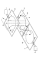
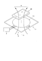
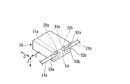
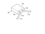
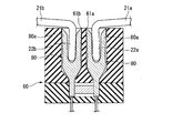
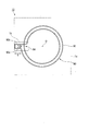
- non-contact electric power transmission device 10 of a 1st embodiment It is a perspective view which shows the usage example of the non-contact electric power transmission device 10 of FIG. It is a perspective view which shows the usage example of the non-contact electric power transmission device 11 of FIG. It is a perspective view which shows the 2nd insulation part 50 vicinity which concerns on 2nd Embodiment. It is a perspective view which shows the 2nd insulation part 60 vicinity which concerns on a comparative example. It is sectional drawing which shows the 2nd insulation part 50 vicinity which concerns on 2nd Embodiment. It is sectional drawing which shows the 2nd insulation part 60 vicinity which concerns on a comparative example. It is explanatory drawing of the shape of the coil 90 which concerns on 3rd Embodiment.
- a non-contact power transmission device 10 shown in FIG. 1 includes a coil 20 and an insulating substrate 1 on which the coil 20 is disposed.
- the coil 20 includes a loop portion 21 formed in a loop shape extending around the central axis O, a first end portion 22a, and a second end portion 22b.
- the non-contact power transmission device 10 generates an alternating magnetic field that penetrates the loop portion 21 when a high-frequency current is passed through the coil 20.
- the loop portion 21 is formed in a shape in which a part of a circular shape centered on the central axis O is interrupted, and both end portions 22a and 22b are located in the portion where the circular shape is interrupted. Both end portions 22 a and 22 b extend in a first direction C that intersects the loop shape of the loop portion 21, and face each other in a second direction F that intersects the first direction C.
- the direction along the central axis O is referred to as the central axis direction Z.
- the side facing the inner side of the loop portion 21 in a plan view viewed from the central axis direction Z is referred to as an inner side, and the opposite side is referred to as an outer side.
- the loop portion 21 and both end portions 22a and 22b of the coil 20 are integrally formed by deforming one metal wire.
- a metal wire for example, a copper wire, a copper-clad steel wire, a copper-clad aluminum wire, or the like can be used.
- a copper wire When a copper wire is used, the loss of energy when a high-frequency current flows through the coil 20 can be suppressed because the electrical resistance of the copper wire is low.
- copper-clad steel wire or copper-clad aluminum wire is used, the thickness of the copper coating is made thicker than the thickness corresponding to the skin depth when high-frequency current flows. Energy loss can be suppressed.
- the metal wire constituting the coil 20 may be a single wire or a stranded wire.
- Conductive connecting portions 23 are disposed on the outer ends of both end portions 22a and 22b, and are connected to both end portions 22a and 22b separately. The connecting portion 23 is electrically connected to both end portions 22a and 22b.
- a capacitor 4 is disposed at the center of the both end portions 22a and 22b in the first direction C, and both end portions of the capacitor 4 are electrically connected to the both end portions 22a and 22b, respectively.
- the capacitance of the capacitor 4 may be set so as to resonate approximately with the inductance of the coil 20 at the drive frequency of the non-contact power transmission device 10.
- the insulating substrate 1 is formed in a rectangular flat plate shape, and includes a first insulating portion 1a in which the loop portion 21 of the coil 20 is disposed, and both ends 22a and 22b of the coil 20, the connecting portion 23, and the capacitor 4 are arranged. And a second insulating portion 1b provided.
- the first insulating part 1a is formed of a synthetic resin material to which a flame retardant is added.
- a flame retardant a phosphorus flame retardant such as phosphate, an inorganic flame retardant such as chlorinated paraffin, aluminum hydroxide or magnesium hydroxide, or a non-halogen organic compound such as silicone compound can be used.
- a synthetic resin material to which a flame retardant is added a polyolefin resin such as a polypropylene resin or a polyethylene resin, or a styrene resin such as an ABS resin can be used.
- the synthetic resin material that constitutes the first insulating portion 1a may be, for example, one that exhibits flame retardancy of disaster prevention grade 3 or higher in the test method specified in JIS A 1322, and is grade 2 disaster prevention or grade 1 disaster prevention. Still good.
- a synthetic resin material to which a flame retardant is added has a low dielectric strength, and the withstand voltage of the synthetic resin material constituting the first insulating portion 1a is less than about 15 kV / mm.
- the second insulating portion 1b is formed of a material having a greater dielectric strength than the material of the first insulating portion 1a.
- the synthetic resin material constituting the second insulating portion 1b include polyethylene (withstand voltage of 18 kV / mm), FRP (19 kV / mm), polypropylene (20 kV / mm), and epoxy resin to which no flame retardant is added. (20 kV / mm), polyacetal (26 kV / mm), polycarbonate (31 kV / mm), and the like can be used.
- the synthetic resin material which comprises the 2nd insulation part 1b does not contain a flame retardant, it shows a flame retardance lower than the synthetic resin material which comprises the 1st insulation part 1a.
- the synthetic resin material constituting the second insulating portion 1b exhibits flame retardancy lower than the disaster prevention class 3 in the test method specified in JIS A 1322.
- the insulating substrate 1 does not have to be rectangular, and may be formed in a circular shape, for example.
- FIG. 2 is an example showing a usage state of the non-contact power transmission device 10, and in the illustrated example, the non-contact power transmission device 10 is used as a so-called repeater.
- the basic configuration of the contactless power transmission devices 11 and 12 illustrated in FIG. 2 is the same as that of the contactless power transmission device 10.
- both end portions 22 a and 22 b of the coil 20 are electrically connected by the coupling portion 23, whereas the non-contact power transmission devices 11 and 12 are provided with the coupling portion 23.
- the non-contact power transmission device 11 is electrically connected to a high frequency power source P
- the non-contact power transmission device 12 is electrically connected to a load L such as a home appliance.
- the non-contact power transmission device 11 operates as a so-called power transmitter, and the non-contact power transmission device 12 operates as a so-called power receiver.
- the non-contact power transmission device 11 when the high frequency power source P supplies the alternating currents I 1 to the coil 11b, an alternating magnetic field g 1 generated in the coil 11b, the coil 20 of the AC magnetic field g 1 is non-contact power transmission device 10 The loop portion 21 is penetrated. Then, an induced current I 2 is generated in the coil 20, and an alternating magnetic field g 2 is generated by the induced current I 2 .
- the non-contact power transmission devices 10 to 12 can transmit power from the high-frequency power source P to the load L in a non-contact manner.
- FIG. 3 is an example showing a use state when the non-contact power transmission device 11 is used alone.
- high-frequency power source P supplies the alternating currents I 1 to a coil 11b of the non-contact power transmission device 11
- an alternating magnetic field g 1 is generated through the coil 11b, not shown in which the alternating magnetic field g 1 is provided in the cellular phone 100 for example Through the receiving coil.
- a secondary battery (not shown) of the mobile phone 100 electrically connected to the power receiving coil is charged. In this way, the secondary battery of the mobile phone 100 can be charged without connecting the mobile phone 100 to the power cord or the like by the non-contact power transmission device 11.
- the contactless power transmission devices 10 to 12 shown in FIGS. 2 and 3 can be used, for example, by being embedded or attached to building materials such as walls and floors, or furniture such as desks.
- building materials such as walls and floors, or furniture such as desks.
- flame resistance is required to prevent the spread of fire in the event of a fire.
- the manufacturing process of the non-contact power transmission device 10 will be described.
- the insulating substrate 1 in which the first insulating portion 1a and the second insulating portion 1b are integrally formed in a flat plate shape is prepared.
- a groove for arranging the coil 20 is formed in the insulating substrate 1.
- the groove may be formed in the same shape as the coil 20 provided in the non-contact power transmission device 10.
- machining or the like can be employed. Or you may form a groove
- the wire constituting the coil 20 is fitted into the groove formed in the insulating substrate 1.
- the wire 20 constituting the coil 20 may be fitted while being deformed according to the shape of the groove.
- the wire may be deformed in advance to match the shape of the groove, and the deformed wire may be fitted into the groove.
- the shape of the wire is held along the groove.
- the loop shape of the coil 20 can be stably formed in a desired shape by fitting the wire into the groove formed in the insulating substrate 1 and maintaining the coil shape. Furthermore, by stabilizing the loop shape of the coil 20, the electrical characteristics of the coil 20 can be stabilized.
- the capacitor 4 and the connecting portion 23 are connected to both end portions 22a and 22b of the coil 20 using, for example, solder.
- condenser 4 and the connection part 23 are electrically connected to both ends 22a and 22b.
- the coil 20 is formed by deforming a copper wire, a restoring force is applied to both end portions 22a and 22b so as to be separated from each other in the second direction F.
- the capacitor 4 is pulled and broken in the second direction F by the restoring force, or the capacitor 4 and the coil 20 It is possible to prevent disconnection between the both end portions 22a and 22b.
- a liquid synthetic resin is poured into the groove in which the wire material of the coil 20 is fitted and cured.
- a liquid resin having the same flame retardance characteristics as that of the first insulating portion 1 a is poured into a groove in a region where the loop portion 21 is disposed, and is cured.
- the loop portion 21 is embedded and sealed in the first insulating portion 1a, and the loop portion 21 contacts the first insulating portion 1a.
- a liquid resin having the same dielectric strength as that of the second insulating portion 1b is poured into a portion where the both end portions 22a and 22b, the capacitor 4 and the connecting portion 23 are disposed in the groove.
- condenser 4, and the connection part 23 are embedded in the 2nd insulation part 1b, and are enclosed.
- substrate 1 before an assembly was formed only by the 1st insulation part 1a, and arrange
- a step of injecting may be employed.
- the non-contact power transmission device 10 can be manufactured by the above manufacturing method.
- the second insulating portion 1b of the insulating substrate 1 is formed of a material having a higher dielectric strength than the first insulating portion 1a. Both end portions 22a and 22b of the coil 20 are disposed on the insulating portion 1b. With this configuration, it is possible to prevent dielectric breakdown from occurring when a high potential difference is generated between both end portions 22a and 22b.
- the loop part 21 which occupies most area among the coils 20 is arrange
- the first insulating portion 1a of the insulating substrate 1 is formed of a synthetic resin material, it is possible to improve the flame retardance of the first insulating portion by adding a flame retardant to the synthetic resin material. Furthermore, since the loop portion 21 of the coil 20 and the first insulating portion 1a are in contact with each other, when the first insulating portion 1a is unexpectedly heated, heat is efficiently applied from the first insulating portion 1a to the coil 20. This heat can be dissipated through the coil 20. Thereby, the temperature rise of the insulating substrate 1 can be suppressed and, for example, the insulating substrate 1 can be prevented from melting.
- the capacitor 4 electrically connected to the both end portions 22a and 22b of the coil 20 is disposed in the second insulating portion 1b having a high dielectric strength in the insulating substrate 1, a high voltage is applied to the capacitor 4. Even when is applied, it is possible to prevent dielectric breakdown from occurring.
- the 1st insulating part 1a in 2nd Embodiment is formed by bonding together the sheet-like film which has a flame retardance.
- the 2nd insulating part 50 of 2nd Embodiment is formed in the substantially rectangular parallelepiped shape.
- the second insulating portion 1b of the first embodiment is formed integrally with the first insulating portion 1a, but the second insulating portion 50 of the second embodiment is formed separately from the first insulating portion 1a. ing.
- a first groove portion 53a and a second groove portion 53b are formed in the center portion in the central axis direction Z of the inner end face in the first direction C of the second insulating portion 50.
- the first groove portion 53a extends from the central wall 54 toward the opposite side of the second groove portion 53b.
- the second groove 53b extends from the central wall 54 toward the opposite side of the first groove 53a.
- the grooves 53 a and 53 b extend from the central portion in the second direction F of the second insulating portion 50 in the direction away from each other in the second direction F.
- a central wall 54 is formed at the central portion in the central axis direction Z and the central portion in the second direction F of the inner end face of the second insulating portion 50.
- the groove portions 53 a and 53 b are formed separately from each other at a distance in the second direction F by the central wall 54.
- a first contact portion 52a and a second contact portion 52b are formed on the inner end face of the second insulating portion 50 in the first direction C.
- the contact portions 52 a and 52 b are formed at both end portions in the central axis direction Z of the second insulating portion 50.
- the contact portions 52a and 52b are adjacent to the groove portions 53a and 53b in the central axis direction Z.
- the contact portions 52a and 52b are formed at a distance equivalent to the wire diameter of the coil 20 in the central axis direction Z.
- the contact portions 52a and 52b extend along the second direction F separately.
- the contact portions 52a and 52b are continuous with the central wall 54 at the central portion in the second direction F.
- a first opening 51a and a second opening 51b that open toward the inside in the first direction C are formed at the center in the second direction F of the bottoms of the grooves 53a and 53b.
- the openings 51 a and 51 b are formed adjacent to the central wall 54. Both ends 22a and 22b of the coil 20 are inserted into the openings 51a and 51b, respectively.
- connecting portions 21a and 21b which are portions respectively connected to both end portions 22a and 22b, are fitted into the groove portions 53a and 53b, respectively. Accordingly, the contact portions 52a and 52b are in contact with the connecting portions 21a and 21b of the loop portion 21 separately from the central axis direction Z.
- the contact portions 52a and 52b sandwich the connecting portions 21a and 21b of the loop portion 21 in the central axis direction Z.
- a first terminal 71 and a second terminal 72 are disposed inside the second insulating portion 50.
- the pair of terminals 71, 72 extend separately from each other along the first direction C from the openings 51 a, 51 b of the second insulating unit 50.
- Each terminal 71, 72 is formed with a first insertion hole 71a and a second insertion hole 72a, respectively.
- Each insertion hole 71a, 72a extends along the first direction C and opens inward.
- the first terminal 71 is formed with a first outer protrusion 71b and a first inner protrusion 71c.
- the first outer protrusion 71b protrudes from the inner wall of the first insertion hole 71a toward the second terminal 72 in the second direction F.
- the first inner protrusion 71c protrudes from the inner wall of the first insertion hole 71a toward the first outer protrusion 71b.
- the second terminal 72 is formed with a second outer protrusion 72b and a second inner protrusion 72c.
- the second outer protrusion 72b protrudes from the inner wall of the second insertion hole 72a toward the first terminal 71 in the second direction F.
- the second inner protrusion 72c protrudes from the inner wall of the second insertion hole 72a toward the second outer protrusion 72b.
- the capacitor 4 is disposed at the outer end of the pair of terminals 71 and 72 in the first direction C, and the capacitor 4 is electrically connected to the pair of terminals 71 and 72 separately.
- the manufacturing process of the non-contact power transmission device 10 in the second embodiment will be described.
- the wire which comprises the coil 20 is prepared, and it deform
- FIG. By deforming the wire into the shape of the coil 20, the loop portion 21 and both end portions 22a and 22b are formed.
- both end portions 22a and 22b of the coil 20 are inserted into the insertion holes 71a and 72a of the pair of terminals 71 and 72 through the openings 51a and 51b of the second insulating portion 50, respectively. To do. Thereby, both end portions 22a and 22b are electrically connected to the pair of terminals 71 and 72 and the capacitor 4 separately.
- the loop shape of the coil 20 is formed by deforming a copper wire, a restoring force in a direction in which both end portions 22a and 22b are separated from each other acts on the coil 20.
- both end portions 22a and 22b are inserted into the insertion holes 71a and 72a, both end portions 22a and 22b are not separated by the restoring force. Further, when both end portions 22a and 22b are inserted into the respective insertion holes 71a and 72a, the connecting portions 21a and 21b of the coil 20 are fitted into the groove portions 53a and 53b of the second insulating portion 50, respectively. At this time, the first contact portion 52a and the second contact portion 52b of the second insulating portion 50 are in contact with the connecting portions 21a and 21b separately from the central axis direction Z, and the shape of the loop portion 21 in the coil 20 is maintained. Is done.
- two films constituting the first insulating portion 1a are prepared.
- a sheet-like adhesive may be attached to these films, or a liquid adhesive may be applied.
- maintained are sandwiched between these two films.
- the two films are bonded to each other. Thereby, the coil 20 and the 2nd insulation part 50 are enclosed with the 1st insulation part 1a.
- the pair of terminals 71 and 72 electrically connected to the both ends 22a and 22b of the coil 20 are large in dielectric strength. Arranged in the second insulating portion 50. With this configuration, even when a high potential difference is generated between the pair of terminals 71 and 72, the occurrence of dielectric breakdown can be prevented. Furthermore, since both the end portions 22a and 22b are separated in the second direction F by the central wall 54 of the second insulating portion 50, the effect of preventing the occurrence of the dielectric breakdown can be achieved more reliably.
- FIG. 4B is a perspective view showing a second insulating portion 60 as a comparative example in which the contact portions 52a and 52b are not formed. Since no contact portion is formed on the second insulating portion 60, the connecting portions 21a and 21b may swing around the openings 61a and 61b, respectively, as shown in FIG. Is difficult to hold. In this state, if the coil 20 is sandwiched from the central axis by two films constituting the first insulating portion 1a, the coil 20 does not have a desired loop shape, and the electrical characteristics of the coil 20 become unstable. There is. On the other hand, according to this embodiment, as shown in FIG.
- the contact portions 52a and 52b sandwich the connecting portions 21a and 21b of the coil 20 in the central axis direction Z. For this reason, it is possible to restrict the connecting portions 21a and 21b from swinging in the central axis direction Z around the openings 51a and 51b. Thereby, it is easy to hold
- FIG. 5B is a cross-sectional view showing a terminal 80 as a comparative example in which the protruding portions 71b, 71c, 72b, 72c are not formed. Since no protruding portion is formed on the inner wall of the insertion hole 80a of the terminal 80, when an external force is applied in the direction of pulling out the both end portions 22a and 22b of the coil 20 from each insertion hole 80a, it is caught and becomes a resistance. Absent. For this reason, both ends 22a and 22b are easy to come off from each insertion hole 80a.
- the outer protrusions 71b and 72b are formed on the terminals 71 and 72, respectively.
- the both end portions 22a and 22b are hooked to the outer projecting portions 71b and 72b by the restoring force that the both end portions 22a and 22b try to separate in the second direction F, and the both end portions 22a and 22b are inserted into the respective insertion holes 71a and 72a. Can be prevented from coming off.
- the inner protrusions 71c and 72c are formed on the terminals 71 and 72, respectively, when the both end portions 22a and 22b are to be removed from the respective insertion holes 71a and 72a, the inner protrusion portions 71c and 72c are both end portions. Friction resistance is generated by contact with 22a and 22b, respectively. As a result, the effect of preventing the end portions 22a and 22b from coming off from the insertion holes 71a and 72a can be achieved more reliably.
- the loop portion 21 in the coil 20 of the first embodiment was formed in a one-loop shape.
- the loop portion 91 in the coil 90 of the third embodiment is formed in a two-turn loop shape.
- the intersecting portion 94 that intersects the end portion 92 b of the coil 90 in plan view and the end portion 92 b are separated from each other in the central axis direction Z.
- Both end portions 92a and 92b and the intersecting portion 94 are disposed in the second insulating portion 1b of the insulating substrate 1, and the second insulating portion 1b is disposed between the intersecting portion 94 and the end portion 92b in the central axis direction Z. Is present.
- the first insulating portion 1a of the insulating substrate 1 is formed of a synthetic resin material.
- the first insulating portion 1a is not limited thereto, and is formed of a material having flame retardance other than the synthetic resin.
- the first insulating portion 1a may be used.
- the shape of the loop portion 21 may not be circular, and may be, for example, a rectangular shape with the central axis O as the centroid in a plan view viewed from the central axis direction Z.
- the capacitor 4 electrically connected to the both end portions 22a and 22b of the coil 20 is disposed in the second insulating portion 1b of the insulating substrate 1.
- the configuration is not limited to this, and a configuration in which the capacitor 4 is not disposed in the second insulating portion 1b may be employed.
- the range of the 2nd insulation part 1b with respect to the 1st insulation part 1a was shown with the broken line in FIG. 1, it is not restricted to this, You may change the range of the 2nd insulation part 1b suitably.
- both end portions 22 a and 22 b extend from the loop portion 21 in the first direction C.
- both end portions 22a and 22b may not extend from a portion where the loop shape of the loop portion 21 is interrupted, and the interrupted portions may be disposed in the second insulating portion 1b.
- the capacitor 4 may be electrically connected to the disconnected portion.
- the coil 20 may be formed in a C shape.
- both ends 22a and 22b are extended in the center axis direction Z. Also good.
- contactless power transmission using the electromagnetic induction method has been described.
- the present invention is not limited to this, and contactless power transmission may be performed using an electromagnetic resonance method.
- the pair of terminals 71 and 72 are provided in the second insulating portion 50 of the insulating substrate 1.
- the present invention is not limited to this, and the pair of terminals 71 and 72 is provided. May not be disposed in the second insulating portion 50. Further, the outer protrusions 71b and 72b or the inner protrusions 71c and 72c may not be formed on the inner walls of the pair of terminals 71 and 72.
- the pair of contact portions 52 a and 52 b are formed in the second insulating portion 50.
- the present invention is not limited to this.
- only one of the contact portions 52 a and 52 b may be formed in the second insulating portion 50.
- contact part 52a, 52b may be formed in the shape of the protrusion which protrudes toward the inner side of the 1st direction C in the position which left
- the central wall 54 may not be formed in the second insulating portion 50, and the groove portions 53 a and 53 b may be continued in the second direction F. Or you may use the 2nd insulating part 50 in which the groove parts 53a and 53b and the contact parts 52a and 52b are not formed.
- the first insulating portion 1a of the insulating substrate 1 is formed by laminating two films.
- the present invention is not limited to this, and other manufacturing processes may be adopted.
- both end portions 22a and 22b of the coil 20 are inserted into the openings 51a and 51b of the second insulating portion 50, respectively, and then set in a mold or the like to be fluidized as the material of the first insulating portion 1a.
- the loop part 91 in the coil 90 was formed in the loop shape of 2 turns, it is not restricted to this, The loop part 91 is formed in the loop shape of 3 turns or more. It may be used.
Landscapes
- Engineering & Computer Science (AREA)
- Power Engineering (AREA)
- Computer Networks & Wireless Communication (AREA)
- Details Of Aerials (AREA)
- Current-Collector Devices For Electrically Propelled Vehicles (AREA)
Abstract
非接触電力伝送デバイスは、ループ状に形成されたループ部と、第1端部および第2端部と、を有するコイルと、前記コイルが配設された絶縁基板と、を備え、前記絶縁基板は、前記ループ部が配設された第1絶縁部と、前記コイルの前記第1端部および前記第2端部が配設された第2絶縁部と、を備え、前記第1絶縁部を構成する部材は、前記第2絶縁部を構成する部材よりも高い難燃性を有し、前記第2絶縁部を構成する部材は、前記第1絶縁部を構成する部材よりも大きな絶縁耐力を有する。
Description
本発明は、非接触電力伝送デバイスに関するものである。
本願は、2016年3月14日に、日本に出願された特願2016-049926号に基づき優先権を主張し、その内容をここに援用する。
本願は、2016年3月14日に、日本に出願された特願2016-049926号に基づき優先権を主張し、その内容をここに援用する。
従来から、電気機器への給電などを非接触電力伝送方式により行う技術が知られている。
例えば特許文献1では、住宅やオフィスなどの建築物に非接触給電システムを備え付け、コンセントなどの接続器の設置を不要にする発明が提案されている。
例えば特許文献1では、住宅やオフィスなどの建築物に非接触給電システムを備え付け、コンセントなどの接続器の設置を不要にする発明が提案されている。
ところで、この種の非接触給電システムでは、コイルと、コイルが配設された絶縁基板と、を備えた非接触電力伝送デバイスを用いる場合がある。この非接触電力伝送デバイスを壁などの建材に取り付けて用いる際に、火災発生時の延焼を防止するために絶縁基板が難燃性を有することが要求される場合がある。また、共振現象を利用する非接触電力伝送方式においては、共振器の両端に共振電圧が発生し、コイルの両端部に高い電圧が印加される。このため、絶縁基板が上記の難燃性に加えて耐電圧性を有することも要求される場合がある。
本発明はこのような事情を考慮してなされたもので、難燃性と耐電圧性とを併せ持つ絶縁基板を備える非接触電力伝送デバイスを提供することを目的とする。
上記課題を解決するために、本発明の第1態様に係る非接触電力伝送デバイスは、ループ状に形成されたループ部と、第1端部および第2端部と、を有するコイルと、前記コイルが配設された絶縁基板と、を備え、前記絶縁基板は、前記コイルのループ部が配設された第1絶縁部と、前記コイルの前記第1端部および前記第2端部が配設された第2絶縁部と、を備え、前記第1絶縁部を構成する部材は、前記第2絶縁部を構成する部材よりも高い難燃性を有し、前記第2絶縁部を構成する部材は、前記第1絶縁部を構成する部材よりも大きな絶縁耐力を有する。
上記態様の非接触電力伝送デバイスによれば、絶縁基板の第2絶縁部を構成する部材が大きな絶縁耐力を有し、この第2絶縁部に、高い電位差が生じるコイルの第1端部および第2端部が配設されている。この構成により、絶縁基板に絶縁破壊が発生するのを防止することができる。さらに、絶縁基板の第1絶縁部を構成する部材が高い難燃性を有し、この第1絶縁部に、コイルのループ部が配設されているから、絶縁基板に難燃性と耐電圧性とを併せ持たせることができる。
ここで、前記第1絶縁部は合成樹脂材料により形成され、前記ループ部と前記第1絶縁部とが互いに接触していてもよい。
この場合、絶縁基板の第1絶縁部は合成樹脂材料により形成されているため、この合成樹脂材料に難燃剤を添加して第1絶縁部の難燃性を向上させることが可能になる。さらに、コイルのループ部と第1絶縁部とが互いに接触しているため、第1絶縁部が不意に加熱された場合に、第1絶縁部からコイルに効率よく熱を伝えて、この熱を、コイルを介して分散させることができる。
また、前記コイルの前記第1端部および前記第2端部は、コンデンサを介して互いに接続されており、前記コンデンサは、前記第2絶縁部に配設されていてもよい。
この場合、コイルの第1端部および第2端部に電気的に接続されたコンデンサが、絶縁基板のうち絶縁耐力の大きい第2絶縁部に配設される。この構成により、コンデンサに高い電圧が印加された場合であっても、絶縁基板に絶縁破壊が発生するのを防止することができる。
また、前記第2絶縁部には、前記コイルの前記第1端部および前記第2端部に各別に電気的に接続された第1端子および第2端子が配設されていてもよい。
この場合、コイルの第1端部および第2端部に各別に電気的に接続された1対の端子が、絶縁基板のうち絶縁耐力の大きい第2絶縁部に配設される。この構成により、1対の端子に高い電圧が印加された場合であっても絶縁破壊の発生を防止することができる。
また、前記コイルの前記第1端部および前記第2端部は、前記ループ部のループ形状に交差する第1方向に延びるとともに、前記第1方向に交差する第2方向で互いに対向し、前記第1端子には、前記コイルの前記第1端部が挿入される第1挿入孔と、前記第1挿入孔の内壁から前記第2方向の前記第2端子側に向けて突出する第1外側突出部と、が形成され、前記第2端子には、前記コイルの前記第2端部が挿入される第2挿入孔と、前記第2挿入孔の内壁から前記第2方向の前記第1端子側に向けて突出する第2外側突出部と、が形成されていてもよい。
この場合、コイルの端部が挿入される端子の挿入孔における内壁には、コイルの両端部が互いに向かい合う方向に向けて突出する外側突出部が形成される。この構成により、ループ状に形成されたコイルに作用する復元力によりコイルの端部が外側突出部に引っ掛かるため、この端部が挿入孔から抜けるのを防止することができる。
また、前記コイルの前記第1端部および前記第2端部は、前記ループ部のループ形状に交差する第1方向に延びるとともに、前記第1方向に交差する第2方向で互いに対向し、前記第2絶縁部には、前記ループ部の内側に向けて開口して前記コイルの前記第1端部が挿入される第1開口部と、前記ループ部の内側に向けて開口して前記コイルの前記第2端部が挿入される第2開口部と、前記ループ部に対して中心軸方向から当接する当接部と、が形成されていてもよい。
この場合、第2絶縁部の当接部が、コイルのループ部に中心軸方向から当接する。この構成により、第2絶縁部の開口部にコイルの端部が挿入された際に、ループ部が開口部を中心として中心軸方向に揺動するのを、当接部が規制する。従って、非接触電力伝送デバイスの製造工程においてコイルのループ形状を保持しやすく、コイルの電気的特性を安定させることができる。
本発明の上記態様によれば、難燃性と耐電圧性とを併せ持つ絶縁基板を備える非接触電力伝送デバイスを提供することができる。
(第1実施形態)
以下、第1実施形態に係る非接触電力伝送デバイス10の構成を、図1を参照しながら説明する。
図1に示す非接触電力伝送デバイス10は、コイル20と、コイル20が配設された絶縁基板1と、を備える。コイル20は、中心軸O周りに延びるループ状に形成されたループ部21と、第1端部22aと、第2端部22bと、を有する。非接触電力伝送デバイス10は、コイル20に高周波電流が流されることにより、ループ部21を貫く交流磁界を発生させるものである。
ループ部21は中心軸Oを中心とする円形状の一部分が途切れた形状に形成されており、この円形状が途切れた部分に、両端部22a、22bが位置している。両端部22a、22bは、ループ部21のループ形状に交差する第1方向Cに延び、第1方向Cに交差する第2方向Fで互いに対向している。
以下、第1実施形態に係る非接触電力伝送デバイス10の構成を、図1を参照しながら説明する。
図1に示す非接触電力伝送デバイス10は、コイル20と、コイル20が配設された絶縁基板1と、を備える。コイル20は、中心軸O周りに延びるループ状に形成されたループ部21と、第1端部22aと、第2端部22bと、を有する。非接触電力伝送デバイス10は、コイル20に高周波電流が流されることにより、ループ部21を貫く交流磁界を発生させるものである。
ループ部21は中心軸Oを中心とする円形状の一部分が途切れた形状に形成されており、この円形状が途切れた部分に、両端部22a、22bが位置している。両端部22a、22bは、ループ部21のループ形状に交差する第1方向Cに延び、第1方向Cに交差する第2方向Fで互いに対向している。
以降の説明では、中心軸Oに沿う方向を中心軸方向Zという。また、前記第1方向Cのうち、中心軸方向Zから見た平面視においてループ部21の内側に向かう側を内側といい、その反対側を外側という。
コイル20のループ部21、両端部22a、22bは、1本の金属製の線材を変形させて一体に形成されている。金属製の線材としては、例えば銅線、銅覆鋼線、銅覆アルミニウム線などを用いることが可能である。銅線を用いた場合には、銅線の電気抵抗が低いために、コイル20に高周波電流が流れた際のエネルギーの損失を抑えることができる。銅覆鋼線や銅覆アルミニウム線を用いた場合には、その銅被覆の厚さを、高周波電流が流れた際の表皮深さに相当する厚さよりも厚くすることで、銅線と同様にエネルギーの損失を抑えることができる。特に、銅被覆の厚さを、高周波電流が流れた際の表皮深さの1.1~2.7倍とすることで、銅線よりもエネルギーの損失を抑えることができる。コイル20を構成する金属製の線材は、単線でもよく、撚線であっても良い。両端部22a、22bの外側の端部には導電性の連結部23が配設され、両端部22a、22bに各別に連なっている。連結部23は、両端部22a、22bに各別に電気的に接続されている。
両端部22a、22bの第1方向Cにおける中央部には、コンデンサ4が配設されており、コンデンサ4の両端部は、両端部22a、22bに各別に電気的に接続されている。コンデンサ4の容量は、非接触電力伝送デバイス10の駆動周波数において、コイル20のインダクタンスとおよそ共振するように設定されるとよい。
両端部22a、22bの第1方向Cにおける中央部には、コンデンサ4が配設されており、コンデンサ4の両端部は、両端部22a、22bに各別に電気的に接続されている。コンデンサ4の容量は、非接触電力伝送デバイス10の駆動周波数において、コイル20のインダクタンスとおよそ共振するように設定されるとよい。
絶縁基板1は矩形の平板状に形成され、コイル20のうちループ部21が配設された第1絶縁部1aと、コイル20のうち両端部22a、22b、連結部23、およびコンデンサ4が配設された第2絶縁部1bと、を備える。
第1絶縁部1aは難燃剤が添加された合成樹脂材料により形成されている。難燃剤としては、リン酸塩などのリン系難燃剤、塩素化パラフィンや水酸化アルミニウムや水酸化マグネシウムなどの無機系難燃剤、シリコーン系化合物などのノンハロゲン有機化合物を用いることができる。また、難燃剤を添加する合成樹脂材料としては、ポリプロピレン樹脂やポリエチレン樹脂等のポリオレフィン樹脂や、ABS樹脂などのスチレン系樹脂を用いることができる。第1絶縁部1aを構成する合成樹脂材料は、例えばJIS A 1322に規定された試験方法において防災3級以上の難燃性を示すものであると良く、防災2級や防災1級であるとなお良い。一般的に、難燃剤が添加された合成樹脂材料は絶縁耐力が低く、第1絶縁部1aを構成する合成樹脂材料の耐電圧は15kV/mm未満程度である。
第2絶縁部1bは第1絶縁部1aの材質よりも絶縁耐力の大きい材質により形成されている。第2絶縁部1bを構成する合成樹脂材料としては、例えば難燃剤が添加されていないポリエチレン(耐電圧が18kV/mm)、FRP(同19kV/mm)、ポリプロピレン(同20kV/mm)、エポキシ樹脂(同20kV/mm)、ポリアセタール(同26kV/mm)、ポリカーボネート(同31kV/mm)などを用いることができる。また、第2絶縁部1bを構成する合成樹脂材料は難燃剤を含まないため、第1絶縁部1aを構成する合成樹脂材料よりも低い難燃性を示す。具体的には、第2絶縁部1bを構成する合成樹脂材料は、JIS A 1322に規定された試験方法において、防災3級より低い難燃性を示す。
なお、絶縁基板1は矩形状である必要はなく、例えば円形状に形成されていてもよい。
第1絶縁部1aは難燃剤が添加された合成樹脂材料により形成されている。難燃剤としては、リン酸塩などのリン系難燃剤、塩素化パラフィンや水酸化アルミニウムや水酸化マグネシウムなどの無機系難燃剤、シリコーン系化合物などのノンハロゲン有機化合物を用いることができる。また、難燃剤を添加する合成樹脂材料としては、ポリプロピレン樹脂やポリエチレン樹脂等のポリオレフィン樹脂や、ABS樹脂などのスチレン系樹脂を用いることができる。第1絶縁部1aを構成する合成樹脂材料は、例えばJIS A 1322に規定された試験方法において防災3級以上の難燃性を示すものであると良く、防災2級や防災1級であるとなお良い。一般的に、難燃剤が添加された合成樹脂材料は絶縁耐力が低く、第1絶縁部1aを構成する合成樹脂材料の耐電圧は15kV/mm未満程度である。
第2絶縁部1bは第1絶縁部1aの材質よりも絶縁耐力の大きい材質により形成されている。第2絶縁部1bを構成する合成樹脂材料としては、例えば難燃剤が添加されていないポリエチレン(耐電圧が18kV/mm)、FRP(同19kV/mm)、ポリプロピレン(同20kV/mm)、エポキシ樹脂(同20kV/mm)、ポリアセタール(同26kV/mm)、ポリカーボネート(同31kV/mm)などを用いることができる。また、第2絶縁部1bを構成する合成樹脂材料は難燃剤を含まないため、第1絶縁部1aを構成する合成樹脂材料よりも低い難燃性を示す。具体的には、第2絶縁部1bを構成する合成樹脂材料は、JIS A 1322に規定された試験方法において、防災3級より低い難燃性を示す。
なお、絶縁基板1は矩形状である必要はなく、例えば円形状に形成されていてもよい。
図2は非接触電力伝送デバイス10の使用状態を示す一例であり、図示の例では非接触電力伝送デバイス10はいわゆる中継器として使用されている。図2に示す非接触電力伝送デバイス11、12の基本的な構成は非接触電力伝送デバイス10と同様である。ただし、非接触電力伝送デバイス10は連結部23によりコイル20の両端部22a、22bが電気的に接続されているのに対して、非接触電力伝送デバイス11、12には連結部23が設けられていない。また、非接触電力伝送デバイス11には高周波電源Pが電気的に接続され、非接触電力伝送デバイス12には例えば家電製品などの負荷Lが電気的に接続されている。
図2において、非接触電力伝送デバイス11はいわゆる送電器として動作し、非接触電力伝送デバイス12はいわゆる受電器として動作する。
以下、各非接触電力伝送デバイス10~12の動作について説明する。非接触電力伝送デバイス11において、高周波電源Pが交流電流I1をコイル11bに供給すると、コイル11bには交流磁界g1が発生し、その交流磁界g1が非接触電力伝送デバイス10のコイル20におけるループ部21を貫く。すると、コイル20には誘導電流I2が発生し、この誘導電流I2によって交流磁界g2が発生する。交流磁界g2は非接触電力伝送デバイス12のコイル12bを貫き、コイル12bには誘導電流I3が発生する。この誘導電流I3がコイル12bに電気的に接続された負荷Lに供給される。以上のようにして、非接触電力伝送デバイス10~12により、高周波電源Pから負荷Lへと非接触により電力を伝送することができる。
以下、各非接触電力伝送デバイス10~12の動作について説明する。非接触電力伝送デバイス11において、高周波電源Pが交流電流I1をコイル11bに供給すると、コイル11bには交流磁界g1が発生し、その交流磁界g1が非接触電力伝送デバイス10のコイル20におけるループ部21を貫く。すると、コイル20には誘導電流I2が発生し、この誘導電流I2によって交流磁界g2が発生する。交流磁界g2は非接触電力伝送デバイス12のコイル12bを貫き、コイル12bには誘導電流I3が発生する。この誘導電流I3がコイル12bに電気的に接続された負荷Lに供給される。以上のようにして、非接触電力伝送デバイス10~12により、高周波電源Pから負荷Lへと非接触により電力を伝送することができる。
図3は非接触電力伝送デバイス11を単独で用いた場合の使用状態を示す一例である。
高周波電源Pが交流電流I1を非接触電力伝送デバイス11のコイル11bに供給すると、コイル11bを貫く交流磁界g1が発生し、その交流磁界g1が例えば携帯電話100に備えられた不図示の受電コイルを貫く。すると、この受電コイルに電気的に接続された携帯電話100の不図示の二次電池などが充電される。このようにして、非接触電力伝送デバイス11により携帯電話100を電源コードなどに接続することなく、携帯電話100の二次電池を充電することができる。
高周波電源Pが交流電流I1を非接触電力伝送デバイス11のコイル11bに供給すると、コイル11bを貫く交流磁界g1が発生し、その交流磁界g1が例えば携帯電話100に備えられた不図示の受電コイルを貫く。すると、この受電コイルに電気的に接続された携帯電話100の不図示の二次電池などが充電される。このようにして、非接触電力伝送デバイス11により携帯電話100を電源コードなどに接続することなく、携帯電話100の二次電池を充電することができる。
図2、図3に示した非接触電力伝送デバイス10~12は、例えば壁や床などの建築材や、机などの家具に埋設あるいは貼り付けて使用することができる。例えば非接触電力伝送デバイス10~12が壁などに埋設される場合には、火災時に延焼を防止するために難燃性が要求される。
次に、非接触電力伝送デバイス10の製造工程について説明する。
先ず、第1絶縁部1aおよび第2絶縁部1bが一体として平板状に形成された絶縁基板1を用意する。そして、絶縁基板1に、コイル20を配設するための溝を形成する。溝の形状は、非接触電力伝送デバイス10に設けるコイル20の形状と同型の溝を形成すればよい。溝を形成する手法としては、例えばマシニング加工等を採用することができる。あるいは、射出成形によって、絶縁基板1の外形を形成するのと同時に溝を形成してもよい。
先ず、第1絶縁部1aおよび第2絶縁部1bが一体として平板状に形成された絶縁基板1を用意する。そして、絶縁基板1に、コイル20を配設するための溝を形成する。溝の形状は、非接触電力伝送デバイス10に設けるコイル20の形状と同型の溝を形成すればよい。溝を形成する手法としては、例えばマシニング加工等を採用することができる。あるいは、射出成形によって、絶縁基板1の外形を形成するのと同時に溝を形成してもよい。
次に、絶縁基板1に形成した溝に、コイル20を構成する線材を嵌め込む。このとき、溝の形状に合わせて、コイル20を構成する線材を変形させながら嵌め込んでもよい。あるいは、予め、線材を溝の形状に合うように変形させておき、変形させた線材を溝に嵌め込んでもよい。溝に線材を嵌め込むと、線材の形状が溝に沿って保持される。このように、絶縁基板1に形成した溝に線材を嵌め込んでコイル形状を保持することにより、コイル20のループ形状を所望の形状に安定して形成することができる。さらに、コイル20のループ形状を安定させることで、コイル20の電気的特性を安定させることができる。
次に、コンデンサ4および連結部23と、コイル20の両端部22a、22bとを例えば半田を用いて接続する。これにより、コンデンサ4および連結部23が両端部22a、22bに電気的に接続される。ここで、コイル20は銅線が変形させられて形成されたものであるため、両端部22a、22bには互いに第2方向Fに離れようとする復元力が作用する。しかしながら、絶縁基板1の溝にコイル20が嵌め込まれてコイル20の形状が保持されることで、コンデンサ4が上記復元力により第2方向Fに引っ張られて破壊されたり、コンデンサ4とコイル20の両端部22a、22bとの間で断線したりすることを防止できる。
次に、コイル20の線材が嵌め込まれた溝に、液状の合成樹脂を流し込んで硬化させる。コイル20のうち、ループ部21が配設された領域の溝には、第1絶縁部1aと同じ難燃特性の液状樹脂を流し込んで硬化させる。これにより、ループ部21が第1絶縁部1aの内部に埋め込まれて封入されるとともに、ループ部21が第1絶縁部1aに接触する。
さらに、前述の溝における両端部22a、22b、コンデンサ4、および連結部23が配設された部分に対して、硬化後には第2絶縁部1bと同じ絶縁耐力をもつ液状樹脂を流し込む。これにより、両端部22a、22b、コンデンサ4、および連結部23が第2絶縁部1bに埋め込まれ、封入される。
なお、組み立て前の絶縁基板1が第1絶縁部1aのみにより形成され、コイル20などを溝に配設した後に、第1絶縁部1aに対して流動化された第2絶縁部1bの合成樹脂を注入する工程を採用してもよい。
さらに、前述の溝における両端部22a、22b、コンデンサ4、および連結部23が配設された部分に対して、硬化後には第2絶縁部1bと同じ絶縁耐力をもつ液状樹脂を流し込む。これにより、両端部22a、22b、コンデンサ4、および連結部23が第2絶縁部1bに埋め込まれ、封入される。
なお、組み立て前の絶縁基板1が第1絶縁部1aのみにより形成され、コイル20などを溝に配設した後に、第1絶縁部1aに対して流動化された第2絶縁部1bの合成樹脂を注入する工程を採用してもよい。
最後に、絶縁基板1の表面を研磨する。研磨することで、液状樹脂によって形成された絶縁基板の表面の凹凸を取り除き、表面を平滑化することができる。
以上の製造方法により、非接触電力伝送デバイス10を製造することができる。
以上の製造方法により、非接触電力伝送デバイス10を製造することができる。
以上説明したように、本実施形態による非接触電力伝送デバイス10によれば、絶縁基板1の第2絶縁部1bが、第1絶縁部1aよりも絶縁耐力の大きい材質によって形成され、この第2絶縁部1bにコイル20の両端部22a、22bが配設されている。この構成により、両端部22a、22b間に高い電位差が生じた場合に、絶縁破壊が発生するのを防止することができる。また、第2絶縁部1bよりも難燃性の高い材質により形成された第1絶縁部1aに、コイル20のうち大部分の面積を占めるループ部21が配設されているから、例えば不意に絶縁基板1が炎に晒された場合であっても延焼を防止することができる。
このようにして、コイル20が配設される絶縁基板1に、難燃性と耐電圧性とを併せ持たせることができる。
このようにして、コイル20が配設される絶縁基板1に、難燃性と耐電圧性とを併せ持たせることができる。
また、絶縁基板1の第1絶縁部1aは合成樹脂材料により形成されているため、この合成樹脂材料に難燃剤を添加して第1絶縁部の難燃性を向上させることが可能になる。さらに、コイル20のループ部21と第1絶縁部1aとが互いに接触しているため、第1絶縁部1aが不意に加熱された場合に、第1絶縁部1aからコイル20に効率よく熱を伝えて、コイル20を介してこの熱を分散させることができる。これにより、絶縁基板1の温度の上昇を抑止して、例えば絶縁基板1が溶融するのを抑制することができる。
また、コイル20の両端部22a、22bに各別に電気的に接続されたコンデンサ4が、絶縁基板1のうち絶縁耐力の大きい第2絶縁部1bに配設されているため、コンデンサ4に高い電圧が印加された場合であっても、絶縁破壊が発生するのを防止することができる。
(第2実施形態)
次に、本発明に係る第2実施形態について説明するが、第1実施形態と基本的な構成は同様である。このため、同様の構成には同一の符号を付してその説明は省略し、異なる点についてのみ説明する。
第2実施形態では、非接触電力伝送デバイス10の製造工程と、第1絶縁部1aおよび第2絶縁部1bの形状と、が第1実施形態と異なる。
次に、本発明に係る第2実施形態について説明するが、第1実施形態と基本的な構成は同様である。このため、同様の構成には同一の符号を付してその説明は省略し、異なる点についてのみ説明する。
第2実施形態では、非接触電力伝送デバイス10の製造工程と、第1絶縁部1aおよび第2絶縁部1bの形状と、が第1実施形態と異なる。
第2実施形態における第1絶縁部1aは、難燃性を有するシート状のフィルムを2枚張り合わせて形成されている。
図4Aに示すように、第2実施形態の第2絶縁部50は略直方体状に形成されている。第1実施形態の第2絶縁部1bは、第1絶縁部1aと一体に形成されていたが、第2実施形態の第2絶縁部50は、第1絶縁部1aとは別体として形成されている。
第2絶縁部50の第1方向Cにおける内側の端面のうち中心軸方向Zにおける中央部には、第1溝部53a、第2溝部53bが形成されている。第1溝部53aは、中央壁54から、第2溝部53bの反対側に向けて延びている。第2溝部53bは、中央壁54から、第1溝部53aの反対側に向けて延びている。このように、溝部53a、53bは第2絶縁部50の第2方向Fにおける中央部から、第2方向Fに互いに離れる方向に延在している。第2絶縁部50の内側の端面のうち中心軸方向Zにおける中央部かつ第2方向Fにおける中央部には、中央壁54が形成されている。溝部53a、53bは中央壁54によって第2方向Fに距離をおいて各別に形成されている。
図4Aに示すように、第2実施形態の第2絶縁部50は略直方体状に形成されている。第1実施形態の第2絶縁部1bは、第1絶縁部1aと一体に形成されていたが、第2実施形態の第2絶縁部50は、第1絶縁部1aとは別体として形成されている。
第2絶縁部50の第1方向Cにおける内側の端面のうち中心軸方向Zにおける中央部には、第1溝部53a、第2溝部53bが形成されている。第1溝部53aは、中央壁54から、第2溝部53bの反対側に向けて延びている。第2溝部53bは、中央壁54から、第1溝部53aの反対側に向けて延びている。このように、溝部53a、53bは第2絶縁部50の第2方向Fにおける中央部から、第2方向Fに互いに離れる方向に延在している。第2絶縁部50の内側の端面のうち中心軸方向Zにおける中央部かつ第2方向Fにおける中央部には、中央壁54が形成されている。溝部53a、53bは中央壁54によって第2方向Fに距離をおいて各別に形成されている。
第2絶縁部50の第1方向Cにおける内側の端面には、第1当接部52aおよび第2当接部52bが形成されている。当接部52a、52bは、第2絶縁部50の中心軸方向Zにおける両端部に形成されている。当接部52a、52bは、溝部53a、53bに対して中心軸方向Zで隣接している。当接部52a、52bは中心軸方向Zにコイル20の線径と同等の距離をおいて形成されている。当接部52a、52bは第2方向Fに沿って各別に延在している。当接部52a、52bは、第2方向Fの中央部において中央壁54と連なっている。
溝部53a、53bの底部のうち第2方向Fにおける中央部には、第1方向Cの内側に向けて開口する第1開口部51aおよび第2開口部51bが形成されている。開口部51a、51bは中央壁54に隣接して形成されている。
コイル20の両端部22a、22bは開口部51a、51bに各別に挿入されている。コイル20のループ部21のうち、両端部22a、22bに各別に連なる部分である連接部21a、21bは溝部53a、53bに各別に嵌め込まれている。これにより、当接部52a、52bはループ部21の連接部21a、21bに対して中心軸方向Zから各別に当接している。当接部52a、52bは、ループ部21の連接部21a、21bを中心軸方向Zで挟んでいる。
溝部53a、53bの底部のうち第2方向Fにおける中央部には、第1方向Cの内側に向けて開口する第1開口部51aおよび第2開口部51bが形成されている。開口部51a、51bは中央壁54に隣接して形成されている。
コイル20の両端部22a、22bは開口部51a、51bに各別に挿入されている。コイル20のループ部21のうち、両端部22a、22bに各別に連なる部分である連接部21a、21bは溝部53a、53bに各別に嵌め込まれている。これにより、当接部52a、52bはループ部21の連接部21a、21bに対して中心軸方向Zから各別に当接している。当接部52a、52bは、ループ部21の連接部21a、21bを中心軸方向Zで挟んでいる。
図5Aに示すように、第2絶縁部50の内部には第1端子71および第2端子72が配設されている。一対の端子71、72は、第2絶縁部50の開口部51a、51bから第1方向Cに沿って各別に延在している。各端子71、72には、第1挿入孔71aおよび第2挿入孔72aがそれぞれ形成されている。各挿入孔71a、72aは第1方向Cに沿って延び、内側に向けて開口している。
第1端子71には、第1外側突出部71bおよび第1内側突出部71cが形成されている。第1外側突出部71bは、第1挿入孔71aの内壁から、第2方向Fの第2端子72側に向けて突出している。第1内側突出部71cは、第1挿入孔71aの内壁から、第1外側突出部71bに向けて突出している。
第2端子72には、第2外側突出部72bおよび第2内側突出部72cが形成されている。第2外側突出部72bは、第2挿入孔72aの内壁から、第2方向Fの第1端子71側に向けて突出している。第2内側突出部72cは、第2挿入孔72aの内壁から、第2外側突出部72bに向けて突出している。
一対の端子71、72の第1方向Cにおける外側の端部にはコンデンサ4が配設され、コンデンサ4は一対の端子71、72に各別に電気的に接続されている。
第1端子71には、第1外側突出部71bおよび第1内側突出部71cが形成されている。第1外側突出部71bは、第1挿入孔71aの内壁から、第2方向Fの第2端子72側に向けて突出している。第1内側突出部71cは、第1挿入孔71aの内壁から、第1外側突出部71bに向けて突出している。
第2端子72には、第2外側突出部72bおよび第2内側突出部72cが形成されている。第2外側突出部72bは、第2挿入孔72aの内壁から、第2方向Fの第1端子71側に向けて突出している。第2内側突出部72cは、第2挿入孔72aの内壁から、第2外側突出部72bに向けて突出している。
一対の端子71、72の第1方向Cにおける外側の端部にはコンデンサ4が配設され、コンデンサ4は一対の端子71、72に各別に電気的に接続されている。
次に、第2実施形態における非接触電力伝送デバイス10の製造工程について説明する。
まず、コイル20を構成する線材を用意し、所望のコイル20の形状となるよう変形させる。線材をコイル20の形状に変形させることで、ループ部21と両端部22a、22bとが形成される。
まず、コイル20を構成する線材を用意し、所望のコイル20の形状となるよう変形させる。線材をコイル20の形状に変形させることで、ループ部21と両端部22a、22bとが形成される。
次に、第2絶縁部50を用意し、コイル20の両端部22a、22bを第2絶縁部50の開口部51a、51bを通して1対の端子71、72の挿入孔71a、72aに各別に挿入する。これにより、両端部22a、22bが、一対の端子71、72およびコンデンサ4に各別に電気的に接続される。ここで、コイル20のループ形状は銅線が変形させられて形成されるため、コイル20には両端部22a、22bが互いに離れる方向の復元力が作用する。しかしながら、両端部22a、22bが挿入孔71a、72aに各別に挿入されているため、復元力により両端部22a、22bが離れることがない。また、両端部22a、22bが各挿入孔71a、72aにそれぞれ挿入されると、コイル20の連接部21a、21bが第2絶縁部50の溝部53a、53bにそれぞれ嵌め込まれる。このとき、第2絶縁部50の第1当接部52aおよび第2当接部52bは連接部21a、21bに中心軸方向Zから各別に当接して、コイル20におけるループ部21の形状が保持される。
次に、第1絶縁部1aを構成する2枚のフィルムを用意する。これらのフィルムには、シート状の接着剤が貼り付けられていてもよく、液状の接着剤が塗布されていてもよい。そして、これら2枚のフィルムの間に、形状が保持されたコイル20および第2絶縁部50を挟む。2枚のフィルムの間にコイル20や第2絶縁部50が介在していない領域では、2枚のフィルム同士が互いに接着される。これにより、コイル20および第2絶縁部50が第1絶縁部1aに封入される。
以上説明したように、本実施形態による非接触電力伝送デバイス10によれば、コイル20の両端部22a、22bに各別に電気的に接続された1対の端子71、72が、絶縁耐力の大きい第2絶縁部50に配設されている。この構成により、1対の端子71、72の間に高い電位差が生じた場合であっても絶縁破壊の発生を防止することができる。さらに、第2絶縁部50の中央壁54によって両端部22a、22bが第2方向Fに隔離されているため、上記絶縁破壊の発生を防止する効果をより確実に奏功させることができる。
また、図4Bは、当接部52a、52bが形成されていない比較例としての第2絶縁部60を示す斜視図である。第2絶縁部60には当接部が形成されていないため、図4Bに示すように連接部21a、21bが開口部61a、61bを中心にそれぞれ揺動する場合があり、ループ部21の形状が保持されづらい。この状態で、コイル20が第1絶縁部1aを構成する2枚のフィルムにより中心軸から挟まれると、コイル20が所望のループ形状とならず、コイル20の電気的特性が不安定になることがある。
一方、本実施形態によれば、図4Aに示すように、当接部52a、52bがコイル20の連接部21a、21bを中心軸方向Zで挟む。このため、連接部21a、21bが開口部51a、51bを中心としてそれぞれ中心軸方向Zに揺動するのを規制することができる。これにより、製造工程においてコイル20のループ形状を保持しやすく、コイル20の電気的特性を安定させることができる。
一方、本実施形態によれば、図4Aに示すように、当接部52a、52bがコイル20の連接部21a、21bを中心軸方向Zで挟む。このため、連接部21a、21bが開口部51a、51bを中心としてそれぞれ中心軸方向Zに揺動するのを規制することができる。これにより、製造工程においてコイル20のループ形状を保持しやすく、コイル20の電気的特性を安定させることができる。
また、図5Bは、突出部71b、71c、72b、72cが形成されていない比較例としての端子80を示す断面図である。端子80の挿入孔80aにおける内壁には突出部が形成されていないため、コイル20の両端部22a、22bを各挿入孔80aから引き抜く方向に外力が作用した場合に、引っかかって抵抗となるものがない。このため、両端部22a、22bが各挿入孔80aから抜けやすい。
一方、本実施形態によれば、図5Aに示すように、端子71、72に外側突出部71b、72bがそれぞれ形成されている。この構成により、両端部22a、22bが第2方向Fに離れようとする復元力によって、両端部22a、22bが外側突出部71b、72bに引っ掛かり、両端部22a、22bが各挿入孔71a、72aから抜けるのを防止することができる。また、端子71、72には内側突出部71c、72cがそれぞれ形成されているため、両端部22a、22bを各挿入孔71a、72aから抜こうとすると、各内側突出部71c、72cが両端部22a、22bとそれぞれ接触して摩擦抵抗を生じる。これにより、挿入孔71a、72aからの両端部22a、22bの抜け防止効果をより確実に奏功させることができる。
(第3実施形態)
次に、第3実施形態に係る非接触電力伝送デバイス13について説明するが、第1実施形態と基本的な構成は同様である。このため、同様の構成には同一の符号を付してその説明は省略し、異なる点についてのみ説明する。
次に、第3実施形態に係る非接触電力伝送デバイス13について説明するが、第1実施形態と基本的な構成は同様である。このため、同様の構成には同一の符号を付してその説明は省略し、異なる点についてのみ説明する。
第1実施形態のコイル20におけるループ部21は1巻のループ形状に形成されていた。これに対して、図6に示すように、第3実施形態のコイル90におけるループ部91は2巻のループ形状に形成されている。ループ部91のうち、コイル90の端部92bと平面視において交差する交差部94と、端部92bと、は中心軸方向Zに離間している。そして、両端部92a、92bおよび交差部94は絶縁基板1の第2絶縁部1bに配設されており、中心軸方向Zにおける交差部94と端部92bとの間には第2絶縁部1bが存在している。これにより、交差部94と端部92bとの間に高い電位差が生じた場合であっても、絶縁破壊が発生するのを防止することができる。
なお、本発明の技術的範囲は前記第1実施形態~第3実施形態に限定されるものではなく、本発明の趣旨を逸脱しない範囲において種々の変更を加えることが可能である。
例えば、前記第1実施形態では、絶縁基板1の第1絶縁部1aは合成樹脂材料により形成されると説明したが、これに限られず、合成樹脂以外の難燃性を有する材質により形成された第1絶縁部1aを用いてもよい。
また、ループ部21の形状は円形状でなくてもよく、例えば中心軸方向Zから視た平面視において中心軸Oを図心とする矩形状などであってもよい。
また、前記第1実施形態では、コイル20の両端部22a、22bに各別に電気的に接続されたコンデンサ4が絶縁基板1の第2絶縁部1bに配設されていると説明したが、これに限られず、コンデンサ4が第2絶縁部1bに配設されない構成を採用してもよい。
また、図1において第1絶縁部1aに対する第2絶縁部1bの範囲を破線で示したが、これに限られず、第2絶縁部1bの範囲を適宜変更してもよい。
また、ループ部21の形状は円形状でなくてもよく、例えば中心軸方向Zから視た平面視において中心軸Oを図心とする矩形状などであってもよい。
また、前記第1実施形態では、コイル20の両端部22a、22bに各別に電気的に接続されたコンデンサ4が絶縁基板1の第2絶縁部1bに配設されていると説明したが、これに限られず、コンデンサ4が第2絶縁部1bに配設されない構成を採用してもよい。
また、図1において第1絶縁部1aに対する第2絶縁部1bの範囲を破線で示したが、これに限られず、第2絶縁部1bの範囲を適宜変更してもよい。
また、前記第1実施形態では、両端部22a、22bがループ部21から第1方向Cに延びている。しかしながら、これに限られず、例えばループ部21のループ形状が途切れた部分から両端部22a、22bが延びておらず、その途切れた部分が第2絶縁部1bに配設されていてもよい。この場合、コンデンサ4はその途切れた部分に各別に電気的に接続されていてもよい。この場合、コイル20はC字状に形成されてもよい。
また、前記第1実施形態では、ループ部21と両端部22a、22bが略同一平面上に形成されていたが、これに限られず、例えば両端部22a、22bが中心軸方向Zに延びていてもよい。
また、前記第1実施形態では、電磁誘導方式による非接触電力伝送について説明したが、これに限られず、電磁界共鳴方式を用いて非接触電力伝送を行ってもよい。
また、前記第1実施形態では、電磁誘導方式による非接触電力伝送について説明したが、これに限られず、電磁界共鳴方式を用いて非接触電力伝送を行ってもよい。
また、前記第2実施形態では、絶縁基板1の第2絶縁部50には1対の端子71、72が配設されていると説明したが、これに限られず、1対の端子71、72が第2絶縁部50に配設されていなくてもよい。
また、一対の端子71、72の内壁には外側突出部71b、72b、または内側突出部71c、72cが形成されていなくてもよい。
また、一対の端子71、72の内壁には外側突出部71b、72b、または内側突出部71c、72cが形成されていなくてもよい。
また、前記第2実施形態では、第2絶縁部50に1対の当接部52a、52b形成されていた。しかしながら、これに限られず、例えば当接部52a、52bのいずれか1方のみが第2絶縁部50に形成されていてもよい。あるいは、当接部52a、52bが、開口部51a、51bから第2方向Fに離れた位置において、各別に第1方向Cの内側に向けて突出する突起状に形成されていてもよい。
また、第2絶縁部50に中央壁54が形成されておらず、溝部53a、53bが第2方向Fに連なっていてもよい。あるいは、溝部53a、53b、および当接部52a、52bが形成されていない第2絶縁部50を用いてもよい。
また、第2絶縁部50に中央壁54が形成されておらず、溝部53a、53bが第2方向Fに連なっていてもよい。あるいは、溝部53a、53b、および当接部52a、52bが形成されていない第2絶縁部50を用いてもよい。
また、前記第2実施形態の製造工程において、2枚のフィルムを張り合わせて絶縁基板1の第1絶縁部1aを形成すると説明したが、これに限られず、他の製造工程を採用してもよい。例えばコイル20の両端部22a、22bを第2絶縁部50の開口部51a、51bに各別に挿入した後、これを金型などにセットして第1絶縁部1aの材料である流動化された合成樹脂を注入する製造工程を採用してもよい。
また、前記第3実施形態では、コイル90におけるループ部91は2巻のループ形状に形成されていたが、これに限られず、ループ部91が3巻以上のループ形状に形成されたコイル90を用いてもよい。
その他、本発明の趣旨を逸脱しない範囲で、上記した実施の形態における構成要素を周知の構成要素に置き換えることは適宜可能であり、また、上記した実施形態や変形例を適宜組み合わせてもよい。
1…絶縁基板 1a…第1絶縁部 1b…第2絶縁部 2…コイル 4…コンデンサ 10~12…非接触電力伝送デバイス 21…ループ部 22a…第1端部 22b…第2端部 50…第2絶縁部 51a…第1開口部 51b…第2開口部 52a…第1当接部 52b…第2当接部 71…第1端子 72…第2端子 71a…第1挿入孔 72a…第2挿入孔 71b…第1外側突出部 72b…第2外側突出部 C…第1方向 F…第2方向 O…中心軸 Z…中心軸方向
Claims (6)
- ループ状に形成されたループ部と、第1端部および第2端部と、を有するコイルと、
前記コイルが配設された絶縁基板と、を備え、
前記絶縁基板は、前記ループ部が配設された第1絶縁部と、前記コイルの前記第1端部および前記第2端部が配設された第2絶縁部と、を備え、
前記第1絶縁部を構成する部材は、前記第2絶縁部を構成する部材よりも高い難燃性を有し、
前記第2絶縁部を構成する部材は、前記第1絶縁部を構成する部材よりも大きな絶縁耐力を有する非接触電力伝送デバイス。 - 前記第1絶縁部は合成樹脂材料により形成され、
前記ループ部と前記第1絶縁部とが互いに接触している、請求項1に記載の非接触電力伝送デバイス。 - 前記コイルの前記第1端部および前記第2端部は、コンデンサを介して互いに接続されており、
前記コンデンサは、前記第2絶縁部に配設されている、請求項1または2に記載の非接触電力伝送デバイス。 - 前記第2絶縁部には、前記コイルの前記第1端部および前記第2端部に各別に電気的に接続された第1端子および第2端子が配設されている、請求項1から3のいずれか1項に記載の非接触電力伝送デバイス。
- 前記コイルの前記第1端部および前記第2端部は、前記ループ部のループ形状に交差する第1方向に延びるとともに、前記第1方向に交差する第2方向で互いに対向し、
前記第1端子には、
前記コイルの前記第1端部が挿入される第1挿入孔と、
前記第1挿入孔の内壁から前記第2方向の前記第2端子側に向けて突出する第1外側突出部と、が形成され、
前記第2端子には、
前記コイルの前記第2端部が挿入される第2挿入孔と、
前記第2挿入孔の内壁から前記第2方向の前記第1端子側に向けて突出する第2外側突出部と、が形成されている、請求項4に記載の非接触電力伝送デバイス。 - 前記コイルの前記第1端部および前記第2端部は、前記ループ部のループ形状に交差する第1方向に延びるとともに、前記第1方向に交差する第2方向で互いに対向し、
前記第2絶縁部には、
前記ループ部の内側に向けて開口して前記コイルの前記第1端部が挿入される第1開口部と、
前記ループ部の内側に向けて開口して前記コイルの前記第2端部が挿入される第2開口部と、
前記ループ部に対して中心軸方向から当接する当接部と、が形成されている、請求項1から5のいずれか1項に記載の非接触電力伝送デバイス。
Applications Claiming Priority (2)
| Application Number | Priority Date | Filing Date | Title |
|---|---|---|---|
| JP2016-049926 | 2016-03-14 | ||
| JP2016049926A JP2017169275A (ja) | 2016-03-14 | 2016-03-14 | 非接触電力伝送デバイス |
Publications (1)
| Publication Number | Publication Date |
|---|---|
| WO2017159379A1 true WO2017159379A1 (ja) | 2017-09-21 |
Family
ID=59850820
Family Applications (1)
| Application Number | Title | Priority Date | Filing Date |
|---|---|---|---|
| PCT/JP2017/008261 Ceased WO2017159379A1 (ja) | 2016-03-14 | 2017-03-02 | 非接触電力伝送デバイス |
Country Status (2)
| Country | Link |
|---|---|
| JP (1) | JP2017169275A (ja) |
| WO (1) | WO2017159379A1 (ja) |
Citations (1)
| Publication number | Priority date | Publication date | Assignee | Title |
|---|---|---|---|---|
| JP2015065632A (ja) * | 2013-08-29 | 2015-04-09 | デクセリアルズ株式会社 | アンテナ装置、複合アンテナ装置、及びこれらを用いた電子機器 |
-
2016
- 2016-03-14 JP JP2016049926A patent/JP2017169275A/ja active Pending
-
2017
- 2017-03-02 WO PCT/JP2017/008261 patent/WO2017159379A1/ja not_active Ceased
Patent Citations (1)
| Publication number | Priority date | Publication date | Assignee | Title |
|---|---|---|---|---|
| JP2015065632A (ja) * | 2013-08-29 | 2015-04-09 | デクセリアルズ株式会社 | アンテナ装置、複合アンテナ装置、及びこれらを用いた電子機器 |
Also Published As
| Publication number | Publication date |
|---|---|
| JP2017169275A (ja) | 2017-09-21 |
Similar Documents
| Publication | Publication Date | Title |
|---|---|---|
| US8922318B1 (en) | Transformer structure | |
| US10596910B2 (en) | Power receiving unit and power supply system having the same | |
| US8736411B2 (en) | Transformer structure | |
| US20150116068A1 (en) | Coil component | |
| US20120154363A1 (en) | Line filter and flat panel display device using the same | |
| EP3038117B1 (en) | Common mode choke coil | |
| US20160315389A1 (en) | Antenna component | |
| US20140001976A1 (en) | Coil component and display device including the same | |
| US8299886B2 (en) | Transformer and electronic apparatus including the same | |
| WO2005117039A1 (ja) | トランス | |
| JP2017130444A (ja) | ケーブルコネクタ | |
| US20150302972A1 (en) | Planar type transformer and switching power supply circuit | |
| US20140160644A1 (en) | Coil component and display device including the same | |
| US7218199B1 (en) | Structure of transformer | |
| KR101039276B1 (ko) | 슬림형 고전압 트랜스포머 | |
| KR100978503B1 (ko) | 슬림형 고전압 트랜스포머 | |
| CN111181254A (zh) | 线圈单元 | |
| WO2017159379A1 (ja) | 非接触電力伝送デバイス | |
| KR101479947B1 (ko) | 변압장치 | |
| JP2016076645A (ja) | 平面コイル | |
| KR101781981B1 (ko) | 하이브리드 트랜스포머 | |
| KR101422930B1 (ko) | 코일 부품 및 이를 구비하는 디스플레이 장치 | |
| US20150116069A1 (en) | Coil component and method of manufacturing the same | |
| KR101779071B1 (ko) | Llc 회로용 트랜스포머 | |
| KR101622746B1 (ko) | 모터의 스테이터 리드선 연결구조 |
Legal Events
| Date | Code | Title | Description |
|---|---|---|---|
| NENP | Non-entry into the national phase |
Ref country code: DE |
|
| 121 | Ep: the epo has been informed by wipo that ep was designated in this application |
Ref document number: 17766382 Country of ref document: EP Kind code of ref document: A1 |
|
| 122 | Ep: pct application non-entry in european phase |
Ref document number: 17766382 Country of ref document: EP Kind code of ref document: A1 |