WO2017159218A1 - 管理装置および電源装置 - Google Patents
管理装置および電源装置 Download PDFInfo
- Publication number
- WO2017159218A1 WO2017159218A1 PCT/JP2017/006109 JP2017006109W WO2017159218A1 WO 2017159218 A1 WO2017159218 A1 WO 2017159218A1 JP 2017006109 W JP2017006109 W JP 2017006109W WO 2017159218 A1 WO2017159218 A1 WO 2017159218A1
- Authority
- WO
- WIPO (PCT)
- Prior art keywords
- voltage
- voltage detection
- circuit
- cells
- battery
- Prior art date
- Legal status (The legal status is an assumption and is not a legal conclusion. Google has not performed a legal analysis and makes no representation as to the accuracy of the status listed.)
- Ceased
Links
Images


Classifications
-
- G—PHYSICS
- G01—MEASURING; TESTING
- G01R—MEASURING ELECTRIC VARIABLES; MEASURING MAGNETIC VARIABLES
- G01R31/00—Arrangements for testing electric properties; Arrangements for locating electric faults; Arrangements for electrical testing characterised by what is being tested not provided for elsewhere
- G01R31/36—Arrangements for testing, measuring or monitoring the electrical condition of accumulators or electric batteries, e.g. capacity or state of charge [SoC]
- G01R31/396—Acquisition or processing of data for testing or for monitoring individual cells or groups of cells within a battery
-
- H—ELECTRICITY
- H02—GENERATION; CONVERSION OR DISTRIBUTION OF ELECTRIC POWER
- H02J—ELECTRIC POWER NETWORKS; CIRCUIT ARRANGEMENTS OR SYSTEMS FOR SUPPLYING OR DISTRIBUTING ELECTRIC POWER; SYSTEMS FOR STORING ELECTRIC ENERGY
- H02J7/00—Circuit arrangements for charging or discharging batteries or for supplying loads from batteries
- H02J7/60—Circuit arrangements for charging or discharging batteries or for supplying loads from batteries including safety or protection arrangements
-
- G—PHYSICS
- G01—MEASURING; TESTING
- G01R—MEASURING ELECTRIC VARIABLES; MEASURING MAGNETIC VARIABLES
- G01R31/00—Arrangements for testing electric properties; Arrangements for locating electric faults; Arrangements for electrical testing characterised by what is being tested not provided for elsewhere
- G01R31/36—Arrangements for testing, measuring or monitoring the electrical condition of accumulators or electric batteries, e.g. capacity or state of charge [SoC]
- G01R31/382—Arrangements for monitoring battery or accumulator variables, e.g. SoC
- G01R31/3835—Arrangements for monitoring battery or accumulator variables, e.g. SoC involving only voltage measurements
-
- H—ELECTRICITY
- H02—GENERATION; CONVERSION OR DISTRIBUTION OF ELECTRIC POWER
- H02J—ELECTRIC POWER NETWORKS; CIRCUIT ARRANGEMENTS OR SYSTEMS FOR SUPPLYING OR DISTRIBUTING ELECTRIC POWER; SYSTEMS FOR STORING ELECTRIC ENERGY
- H02J7/00—Circuit arrangements for charging or discharging batteries or for supplying loads from batteries
- H02J7/50—Circuit arrangements for charging or discharging batteries or for supplying loads from batteries acting upon multiple batteries simultaneously or sequentially
- H02J7/52—Circuit arrangements for charging or discharging batteries or for supplying loads from batteries acting upon multiple batteries simultaneously or sequentially for charge balancing, e.g. equalisation of charge between batteries
Definitions
- the present invention relates to a management device that manages the state of a power storage module such as a battery, and a power supply device that includes the management device.
- HV hybrid vehicles
- PSV plug-in hybrid vehicles
- EV electric vehicles
- a voltage detection circuit for detecting the voltage of each battery cell is provided (see, for example, Patent Document 1). Between a voltage detection line connecting each battery cell and the voltage detection circuit, at least one of a capacitive element for ESD (Electro-Static Discharge) countermeasure and a capacitive element for a filter is connected. The detected voltage of each battery cell is used for charge / discharge control, cell voltage equalization control, and the like.
- ESD Electro-Static Discharge
- Detecting the disconnection of the voltage detection line of the assembled battery is an indispensable item for system failure detection.
- the sum of the voltages of two adjacent battery cells connected to the voltage detection line is divided by two capacitive elements having the same capacitance value. For this reason, each voltage supplied to the voltage detection circuit is almost the same as in the case where no disconnection occurs. Therefore, when a capacitive element is connected between the voltage detection lines, it is difficult to detect disconnection only by detecting the voltage of each battery cell.
- the present invention has been made in view of such a situation, and an object thereof is to provide a technique capable of detecting disconnection more reliably.
- a management device is a voltage detection circuit that is connected to each node of a plurality of cells connected in series by a voltage detection line and detects each voltage of the plurality of cells. And a plurality of capacitor circuits respectively connected between the two voltage detection lines connected to each cell. Two capacitor circuits corresponding to two adjacent cells have different capacitance values.
- disconnection can be detected more reliably.
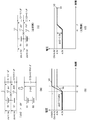
- FIG. 2A is a circuit diagram for explaining the operation when the voltage detection line L2 is disconnected and charged in the power supply device of FIG. 1
- FIG. 2B is a circuit diagram of FIG.
- FIG. 2C is a circuit diagram for explaining the operation when the voltage detection line L2 is disconnected and charged in the power supply device of the comparative example
- FIG. 2D is a circuit diagram of FIG.
- 3A is a circuit diagram for explaining an operation when the voltage detection line L2 is disconnected and discharged in the power supply device of FIG. 1
- FIG. 3B is a circuit diagram of FIG.
- FIG. 3C is a circuit diagram for explaining an operation when the voltage detection line L2 is disconnected and discharged in the power supply device of the comparative example
- FIG. 3D is a circuit diagram of FIG. It is a figure which shows the change of the voltage of.
- FIG. 1 is a circuit diagram showing a configuration of a power supply apparatus 100 according to an embodiment.
- the power supply apparatus 100 can be mounted on a vehicle as a power source such as a hybrid vehicle or an electric vehicle.
- the power supply device 100 includes an assembled battery (power storage module) 10 and a battery management device (management device) 30.
- the assembled battery 10 and the battery management device 30 are connected by a wire harness 20.
- the assembled battery 10 has a plurality of battery cells (cells) connected in series.
- battery cells S1 to S4 connected in series will be described, and illustration and description of other battery cells are omitted.
- a lithium ion battery is assumed as the type of battery.
- 200V or more is the mainstream, and battery cells are often used in 60 series or more.
- a load and a charging circuit are connected between both ends of the assembled battery 10. The assembled battery 10 is discharged to a load and charged by a charging circuit.
- the battery management device 30 includes a plurality of capacitor circuits CA1 to CA4, a voltage detection circuit 32, and a control circuit 34. Regarding the battery management device 30, the configuration corresponding to the battery cells S1 to S4 will be described, and illustrations and descriptions of configurations corresponding to the other battery cells are omitted.
- the battery management device 30 manages the assembled battery 10.
- the battery management device 30 is configured on a printed wiring board, for example.
- Each node of the plurality of battery cells S1 to S4 and the plurality of voltage input terminals VP1 to VP5 of the voltage detection circuit 32 are connected by voltage detection lines L1 to L5, respectively.
- the voltage detection lines L1 to L5 are configured by printed wiring inside the battery management device 30, and are configured by the wire harness 20 outside the battery management device 30.
- the plurality of capacitor circuits CA1 to CA4 are respectively connected between two voltage detection lines connected to the battery cells S1 to S4. That is, the capacitor circuit CA1 is connected between the two voltage detection lines L1, L2 connected to the battery cell S1. Capacitor circuits CA2 to CA4 are similarly connected.
- Each of the plurality of capacitor circuits CA1 to CA4 includes an electrostatic discharge protection circuit that absorbs a discharge pulse accompanying electrostatic discharge and a low-pass filter circuit having a predetermined frequency characteristic. That is, the capacitor circuit CA1 includes an electrostatic discharge protection circuit E1 and a low-pass filter circuit LP1.
- the capacitor circuits CA2 to CA4 have the same configuration.
- the electrostatic discharge protection circuits E1 to E4 include first capacitive elements C1 to C4, respectively.
- the plurality of first capacitor elements C1 to C4 are ESD protection elements. Therefore, the capacitance values of the first capacitance elements C1 to C4 are set to values that can ensure the necessary electrostatic withstand voltage.
- the plurality of first capacitive elements C1 to C4 are respectively connected between two voltage detection lines connected to the battery cells S1 to S4. In the example shown in FIG. 1, the first capacitive element C1 is connected between the voltage detection line L1 and the voltage detection line L2.
- the first capacitive element C2 is connected between the voltage detection line L2 and the voltage detection line L3, between the voltage detection line L3 and the voltage detection line L4, and between the voltage detection line L4 and the voltage detection line L5, respectively. That is, the plurality of first capacitor elements C1 to C4 are respectively connected between both ends of the corresponding battery cell.
- the first capacitive elements C1 to C4 are arranged on the battery cells S1 to S4 side with respect to the resistors R1 to R5.
- the capacitance values of the two first capacitor elements C1 and C2 corresponding to the two adjacent battery cells S1 and S2 are different from each other.
- the capacitance values of the two first capacitor elements C2 and C3 corresponding to the two adjacent battery cells S2 and S3 are different from each other.
- the capacitance values of the two first capacitor elements C3 and C4 corresponding to the two adjacent battery cells S3 and S4 are different from each other.
- two electrostatic protection circuits corresponding to two adjacent battery cells have first capacitance elements having different capacitance values.
- the capacitance values of the plurality of first capacitor elements C1 and C3 corresponding to every other plurality of battery cells S1 and S3 may be substantially equal to each other.
- the capacitance values of the plurality of first capacitive elements C2 and C4 corresponding to every other plurality of battery cells S2 and S4 may be substantially equal to each other.
- the capacitance value is not particularly limited.
- the capacitance values of the first capacitance elements C1 and C3 are about 0.1 ⁇ F
- the capacitance values of the first capacitance elements C2 and C4 are about 0.1 ⁇ F. It may be 01 ⁇ F.
- the plurality of voltage detection lines L1 to L5 are connected to the plurality of voltage input terminals VP1 to VP5 of the voltage detection circuit 32 through low-pass filter circuits LP1 to LP4, respectively.
- the low-pass filter circuits LP1 to LP4 suppress noise in the voltage detection lines L1 to L5.
- the low-pass filter is configured by an RC circuit.
- the low-pass filter circuits LP1 to LP4 each include a resistor and a second capacitance element. Resistors R1 to R5 are connected in series to the plurality of voltage detection lines L1 to L5, respectively.
- the plurality of second capacitive elements C11 to C14 are connected between the two voltage detection lines connected to the respective battery cells S1 to S4 on the voltage detection circuit 32 side of the resistors R1 to R5. That is, the second is between the voltage detection line L1 and the voltage detection line L2, between the voltage detection line L2 and the voltage detection line L3, between the voltage detection line L3 and the voltage detection line L4, and between the voltage detection line L4 and the voltage detection line L5.
- the capacitive element C11, the second capacitive element C12, the second capacitive element C13, and the second capacitive element C14 are connected.
- the resistance values of the resistors R1 to R5 are substantially equal to each other.
- the capacitance values of the second capacitive elements C11 to C14 are substantially equal to each other.
- the capacitance value of the capacitor circuit CA1 is the sum of the capacitance value of the first capacitance element C1 and the capacitance value of the second capacitance element C2.
- the plurality of capacitor circuits CA1 and CA3 corresponding to every other plurality of battery cells S1 and S3 may have substantially the same capacitance value.
- the plurality of capacitor circuits CA2 and CA4 corresponding to every other plurality of battery cells S2 and S4 may have substantially the same capacitance value.
- the voltage detection circuit 32 is connected to each node of the plurality of battery cells S1 to S4 connected in series, and detects the voltage of each of the plurality of battery cells S1 to S4. Specifically, the voltage detection circuit 32 detects each voltage of the plurality of voltage input terminals VP1 to VP5. The detected voltages of the battery cells S1 to S4 are transmitted to the control circuit 34.
- the voltage detection circuit 32 includes an ASIC (Application (Specific Integrated Circuit) that is a dedicated custom IC.
- the control circuit 34 performs battery control such as cell voltage equalization control with reference to the voltage acquired from the voltage detection circuit 32. Further, when detecting an abnormality in each voltage of the battery cells S1 to S4, the control circuit 34 notifies an upper level control device (not shown) of an abnormality detection signal indicating the abnormality of the voltage. When the upper control device is notified of the abnormality detection signal, it performs necessary measures such as stopping charging / discharging of the assembled battery 10. Specifically, the control circuit 34 outputs an abnormality detection signal when the voltage of any of the plurality of battery cells S1 to S4 is lower than the first detection voltage UV and higher than the second detection voltage OV. The second detection voltage OV is higher than the first detection voltage UV.
- the control circuit 34 is configured by a CPU, a logic circuit, or a combination thereof.
- FIG. 2A is a circuit diagram for explaining the operation when the voltage detection line L2 is disconnected and charged in the power supply apparatus 100 of FIG. 1, and FIG. 2B is a circuit diagram of FIG. It is a figure which shows the change of the voltage of a circuit.
- the upper circuit shows only the part related to the following description of the power supply apparatus 100, and the lower circuit is an equivalent circuit of the upper circuit.
- the capacitive element C12x is a combined capacitance of the first capacitive elements C1 and C2.
- each voltage Vs of the battery cells S1 and S2 before charging is 4V, and it is assumed that each voltage Vs has increased to 4.3V by charging from time t1 to t2. That is, each voltage change amount ⁇ V of the battery cells S1 and S2 due to charging is 0.3V.
- the voltage change amount ⁇ V2 due to the charging of the first capacitive element C2 having a relatively small capacitance value has a relatively large capacitance value.
- the voltage change amount ⁇ V1 due to the charging of the first capacitor element C1 is larger.
- ⁇ V1 is 0.0546V and ⁇ V2 is 0.546V when calculated in consideration of the capacitive element C12x.
- ⁇ V2 is larger than ⁇ V.
- the second detection voltage OV is 4.4V.
- the control circuit 34 can output an abnormality detection signal.
- FIG. 2C is a circuit diagram for explaining the operation when the voltage detection line L2 is disconnected and charged in the power supply device of the comparative example
- FIG. 2D is a circuit diagram of FIG. It is a figure which shows the change of the voltage of.
- the capacitance values of the plurality of first capacitive elements are substantially equal to each other, and other configurations are the same as those of the present embodiment.
- the voltage V2 across the first capacitive element C2 is equal to the voltage Vs of the battery cell S2 even after charging. equal. Therefore, no abnormality detection signal is output at this timing.
- the voltage V2 is different from the voltage Vs of the battery cell S2.
- the voltage V1 is also different from the voltage Vs of the battery cell S1. Therefore, the voltage Vs is not correctly controlled in the battery cells S1 and S2 in which the correct voltage Vs is not detected. Therefore, when time elapses, the voltage Vs of the battery cells S1 and S2 may become higher than the second detection voltage OV.
- an abnormality detection signal can be output before the voltage Vs of the battery cell S2 becomes higher than the second detection voltage OV. Therefore, necessary measures such as stopping charging / discharging of the assembled battery 10 are taken. This can be done faster than the comparative example.
- FIG. 3A is a circuit diagram for explaining an operation when the voltage detection line L2 is disconnected and discharged in the power supply apparatus 100 of FIG. 1, and FIG. 3B is a circuit diagram of FIG. It is a figure which shows the change of the voltage of a circuit.
- each voltage Vs of the battery cells S1 and S2 before discharge is 3V, and that each voltage Vs is reduced to 2.7V due to discharge from time t3 to t4. That is, the voltage change amount ⁇ V of each of the battery cells S1, S2 due to the discharge is 0.3V.
- the voltage change amount ⁇ V2 due to the discharge of the first capacitive element C2 having a small capacitance value is a first capacitive element C1 having a large capacitance value. It is larger than the voltage change amount ⁇ V1 due to the discharge.
- ⁇ V1 is 0.0546V and ⁇ V2 is 0.546V.
- ⁇ V2 is larger than ⁇ V.
- the first detection voltage UV is 2.5V.
- the control circuit 34 can output an abnormality detection signal.
- FIG. 3C is a circuit diagram for explaining an operation when the voltage detection line L2 is disconnected and discharged in the power supply device of the comparative example
- FIG. 3D is a circuit diagram of FIG. It is a figure which shows the change of the voltage of.
- the voltage V2 across the first capacitive element C2 is equal to the voltage Vs of the battery cell S2 even after discharge. equal. Therefore, no abnormality detection signal is output at this timing.
- the voltage Vs of the battery cells S1 and S2 may be lower than the first detection voltage UV.
- the abnormality detection signal can be output before the voltage Vs of the battery cell S2 becomes lower than the first detection voltage UV, so that the necessary correspondence can be performed earlier than the comparative example.
- the control circuit 34 can output an abnormality detection signal. Accordingly, when the first capacitive elements C1 to C4 are connected between the voltage detection lines, the disconnection can be detected more reliably.
- the battery management device 30 can be realized by setting the capacitance values of the plurality of first capacitance elements C1 to C4 as the ESD protection elements as described above, a new circuit element is added to the comparative example described above. There is no need. Moreover, there is no possibility that the current consumption of the battery management device 30 increases compared to the comparative example. Even if the capacitance values of the first capacitance elements C1 and C3 are different from the capacitance values of the first capacitance elements C2 and C4, the voltage detection characteristics of the voltage detection circuit 32 are hardly affected.
- the capacitance values of the first capacitance elements C1 to C4 are two types, an increase in cost can be suppressed as compared with the comparative example using the first capacitance element having one capacitance value, and the manufacturing process is reduced. The complexity can be suppressed.
- the battery management device 30 can also be applied to use for managing the power storage modules in the stationary power storage system.
- the plurality of battery cells S1 to S4 may be capacitors (capacitors) such as electric double layer capacitors.
- the relationship between the capacitance values of the plurality of first capacitor elements C1 to C4 is not particularly limited.
- the capacitance values of the plurality of first capacitance elements corresponding to every second battery cell may be substantially equal, or the capacitance values of all the first capacitance elements C1 to C4 may be different from each other. .
- the capacitance values of the two first capacitor elements corresponding to the two adjacent battery cells are different from each other with respect to the plurality of first capacitor elements C1 to C4 that are ESD protection elements.
- the capacitance values of the plurality of first capacitance elements C1 to C4 are substantially equal to each other, and the two second capacitance elements C11 to C14 constituting the low-pass filter correspond to the two second capacitance cells corresponding to two adjacent battery cells.
- the capacitance values of the two capacitors may be different from each other. In this case, since the cut-off frequencies of the plurality of low-pass filters are different from each other, the capacitance value may be set so as to satisfy the necessary noise removal characteristics.
- the capacitance values of the two first capacitor elements corresponding to the two adjacent battery cells are different from each other, and the capacitance values of the two second capacitor elements corresponding to the two adjacent battery cells are different from each other. Also good.
- the two combined capacity values corresponding to the two adjacent battery cells may be made different from each other.
- a voltage detection circuit (32) is connected to each node of the plurality of cells (S1 to S4) connected in series by voltage detection lines (L1 to L5) and detects the voltage of each of the plurality of cells (S1 to S4).
- a plurality of capacitor circuits (CA1 to CA4) connected between two voltage detection lines (L1 and L2, L2 and L3, L3 and L4, L4 and L5) connected to each cell (S1 to S4);
- Two capacitor circuits (CA1 and CA2, CA2 and CA3, CA3 and CA4) corresponding to two adjacent cells (S1 and S2, S2 and S3, S3 and S4) have different capacitance values.
- a management device (30) characterized by the above. According to this, it is possible to detect disconnection more reliably.
- a plurality of capacitor circuits (CA1 and CA3, CA2 and CA4) corresponding to every other cell (S1 and S3, S2 and S4) have substantially the same capacitance value, respectively.
- the management device (30) according to 1. According to this, since there are two types of capacitance values of the capacitor circuits (CA1 to CA4), it is possible to suppress an increase in cost and to suppress a complicated manufacturing process.
- Each of the plurality of capacitor circuits (CA1 to CA4) includes an electrostatic discharge protection circuit (E1 to E4) that absorbs a discharge pulse accompanying electrostatic discharge, and a low-pass filter circuit (LP1 to LP4) having a predetermined frequency characteristic.
- the management apparatus (30) according to item 1 or 2, characterized by having C1 and C2, C2 and C3, and C3 and C4). According to this, the frequency characteristics of the low-pass filter circuits (LP1 to LP4) are made substantially equal, and the two capacitor circuits (CA1 and CA2, CA2 and CA3, CA3 and CA4) have different capacitance values. Therefore, the voltage detection characteristic of the voltage detection circuit (32) can be hardly affected.
- the management device (30) according to any one of items 1 to 3, which manages the power storage module (10);
- a power supply device (100) comprising: According to this, the power supply device (100) which can detect a disconnection more reliably can be provided.
- S1 to S4 battery cells, L1 to L5 ... voltage detection lines, CA1 to CA4 ... capacitor circuits, E1 to E4 ... electrostatic discharge protection circuits, C1 to C4 ... first capacitance elements, LP1 to LP4 ... low pass filter circuits, C11 to C14: second capacitance element, R1 to R5: resistance, 10: assembled battery, 30: battery management device, 32: voltage detection circuit, 34: control circuit, 100: power supply device.
Landscapes
- Engineering & Computer Science (AREA)
- Power Engineering (AREA)
- Physics & Mathematics (AREA)
- General Physics & Mathematics (AREA)
- Charge And Discharge Circuits For Batteries Or The Like (AREA)
- Secondary Cells (AREA)
- Testing Of Short-Circuits, Discontinuities, Leakage, Or Incorrect Line Connections (AREA)
- Measurement Of Current Or Voltage (AREA)
- Tests Of Electric Status Of Batteries (AREA)
- Emergency Protection Circuit Devices (AREA)
Abstract
より確実に断線検出できる技術を提供するために、管理装置(30)は、電圧検出回路(32)と複数のキャパシタ回路(CA1~CA4)とを備える。電圧検出回路(32)は、直列接続された複数のセル(S1~S4)の各ノードに電圧検出線(L1~L5)で接続され、当該複数のセル(S1~S4)のそれぞれの電圧を検出する。複数のキャパシタ回路(CA1~CA4)は、各セル(S1~S4)に接続された2本の電圧検出線間にそれぞれ接続される。隣接する2つのセルに対応する2つのキャパシタ回路は、互いに異なる容量値を有している。
Description
本発明は、電池などの蓄電モジュールの状態を管理する管理装置、および、その管理装置を備える電源装置に関する。
近年、ハイブリッド車(HV)、プラグインハイブリッド車(PHV)、電気自動車(EV)が普及してきている。これらの車にはキーデバイスとして二次電池が搭載される。車載用二次電池としては主に、ニッケル水素電池およびリチウムイオン電池が普及している。今後、エネルギー密度が高いリチウムイオン電池の普及が加速すると予想される。
リチウムイオン電池は常用領域と使用禁止領域が近接しているため、他の種類の電池より厳格な電圧管理が必要である。複数のリチウムイオン電池セルが直列に接続された組電池を使用する場合、各電池セルの電圧を検出するための電圧検出回路が設けられる(例えば、特許文献1参照)。各電池セルと電圧検出回路を接続する電圧検出線間には、ESD(Electro-Static Discharge)対策用の容量素子とフィルタ用の容量素子の少なくとも何れかが接続される。検出される各電池セルの電圧は、充放電制御およびセル電圧の均等化制御などに使用される。
組電池の電圧検出線の断線検出は、システムの故障検出の必須項目である。しかし、ある電圧検出線が断線した場合、この電圧検出線に接続されている隣接する2つの電池セルの電圧の和は、容量値が等しい2つの容量素子によって分圧される。そのため、電圧検出回路に供給される各電圧は、断線していない場合とほぼ同じである。よって、電圧検出線間に容量素子が接続されている場合、各電池セルの電圧を検出するのみでは、断線検出は困難である。
本発明はこうした状況に鑑みなされたものであり、その目的は、より確実に断線検出できる技術を提供することにある。
上記課題を解決するために、本発明のある態様の管理装置は、直列接続された複数のセルの各ノードに電圧検出線で接続され、当該複数のセルのそれぞれの電圧を検出する電圧検出回路と、各セルに接続された2本の電圧検出線間にそれぞれ接続された複数のキャパシタ回路とを備える。隣接する2つのセルに対応する2つのキャパシタ回路は、互いに異なる容量値を有している。
本発明によれば、より確実に断線検出できる。
図1は、一実施形態に係る電源装置100の構成を示す回路図である。電源装置100は、例えば、ハイブリッド車、電気自動車などの動力源として車両に搭載することができる。電源装置100は、組電池(蓄電モジュール)10および電池管理装置(管理装置)30を備える。組電池10と電池管理装置30間はワイヤーハーネス20により接続される。
組電池10は直列接続された複数の電池セル(セル)を有する。本実施形態では、直列接続された4つの電池セルS1~S4について説明し、他の電池セルは図示および説明を省略する。また電池の種別としてリチウムイオン電池を想定する。ハイブリッド車や電気自動車に搭載される組電池10は200V以上が主流であり、電池セルは60直列以上で使用されることが多い。組電池10の両端間には、図示を省略した負荷および充電回路が接続される。組電池10は、負荷に放電し、また、充電回路によって充電される。
電池管理装置30は、複数のキャパシタ回路CA1~CA4と、電圧検出回路32と、制御回路34とを備える。電池管理装置30に関しても、電池セルS1~S4に対応する構成について説明し、他の電池セルに対応する構成は図示および説明を省略する。電池管理装置30は組電池10を管理する。電池管理装置30は、例えばプリント配線基板上に構成される。
複数の電池セルS1~S4の各ノードと、電圧検出回路32の複数の電圧入力端子VP1~VP5はそれぞれ電圧検出線L1~L5で接続される。電圧検出線L1~L5は、電池管理装置30の内部ではプリント配線で構成され、電池管理装置30の外部ではワイヤーハーネス20で構成される。
複数のキャパシタ回路CA1~CA4は、各電池セルS1~S4に接続された2本の電圧検出線間にそれぞれ接続される。即ちキャパシタ回路CA1は、電池セルS1に接続された2本の電圧検出線L1,L2間に接続される。キャパシタ回路CA2~CA4も同様に接続される。
複数のキャパシタ回路CA1~CA4のそれぞれは、静電気放電に伴う放電パルスを吸収する静電気放電保護回路と、所定の周波数特性を有するローパスフィルタ回路とを含む。即ちキャパシタ回路CA1は、静電気放電保護回路E1と、ローパスフィルタ回路LP1とを含む。キャパシタ回路CA2~CA4も同様の構成を有する。
静電気放電保護回路E1~E4は、それぞれ第1容量素子C1~C4を含む。複数の第1容量素子C1~C4は、ESD保護素子である。そのため第1容量素子C1~C4の容量値は、必要な静電耐圧を確保できる値に設定される。複数の第1容量素子C1~C4は、各電池セルS1~S4に接続された2本の電圧検出線間にそれぞれ接続される。図1に示す例では、電圧検出線L1と電圧検出線L2間に第1容量素子C1が接続される。電圧検出線L2と電圧検出線L3間、電圧検出線L3と電圧検出線L4間、電圧検出線L4と電圧検出線L5間にも同様に、それぞれ第1容量素子C2、第1容量素子C3、第1容量素子C4が接続される。即ち、複数の第1容量素子C1~C4は、対応する電池セルの両端間にそれぞれ接続される。第1容量素子C1~C4は、抵抗R1~R5より電池セルS1~S4側に配置される。
隣接する2つの電池セルS1,S2に対応する2つの第1容量素子C1,C2の容量値は、互いに異なっている。隣接する2つの電池セルS2,S3に対応する2つの第1容量素子C2,C3の容量値は、互いに異なっている。隣接する2つの電池セルS3,S4に対応する2つの第1容量素子C3,C4の容量値は、互いに異なっている。このように、隣接する2つの電池セルに対応する2つの静電気保護回路は、互いに異なる容量値の第1容量素子を有している。
なお、1つおきの複数の電池セルS1,S3に対応する複数の第1容量素子C1,C3の容量値は、それぞれ実質的に等しくてもよい。1つおきの複数の電池セルS2,S4に対応する複数の第1容量素子C2,C4の容量値は、それぞれ実質的に等しくてもよい。容量素子の容量値を実質的に等しくすることで、ハードウェアを共通化することができ、コスト低減などの効果が期待できる。
このような関係を満たす限り、容量値は特に限定されないが、例えば、第1容量素子C1,C3の容量値は約0.1μFであり、第1容量素子C2,C4の容量値は約0.01μFであってもよい。
複数の電圧検出線L1~L5は、ローパスフィルタ回路LP1~LP4を介して電圧検出回路32の複数の電圧入力端子VP1~VP5にそれぞれ接続される。ローパスフィルタ回路LP1~LP4は、電圧検出線L1~L5のノイズを抑制する。図1に示す例ではローパスフィルタをRC回路で構成している。具体的にはローパスフィルタ回路LP1~LP4は、それぞれ抵抗と第2容量素子とを含む。複数の電圧検出線L1~L5にそれぞれ抵抗R1~R5が直列に接続される。抵抗R1~R5より電圧検出回路32側において、複数の第2容量素子C11~C14は、各電池セルS1~S4に接続された2本の電圧検出線間にそれぞれ接続される。つまり、電圧検出線L1と電圧検出線L2間、電圧検出線L2と電圧検出線L3間、電圧検出線L3と電圧検出線L4間、電圧検出線L4と電圧検出線L5間に、それぞれ第2容量素子C11、第2容量素子C12、第2容量素子C13、第2容量素子C14が接続される。抵抗R1~R5の抵抗値は、それぞれ実質的に等しい。第2容量素子C11~C14の容量値は、それぞれ実質的に等しい。
このように、隣接する2つの電池セルに対応する2つのキャパシタ回路は、互いに異なる容量値を有している。キャパシタ回路CA1の容量値とは、第1容量素子C1の容量値と第2容量素子C2の容量値との和である。キャパシタ回路CA2~CA4の容量値も同様である。また、1つおきの複数の電池セルS1,S3に対応する複数のキャパシタ回路CA1,CA3は、それぞれ実質的に等しい容量値としてもよい。1つおきの複数の電池セルS2,S4に対応する複数のキャパシタ回路CA2,CA4は、それぞれ実質的に等しい容量値としてもよい。
電圧検出回路32は、直列接続された複数の電池セルS1~S4の各ノードに接続され、複数の電池セルS1~S4のそれぞれの電圧を検出する。具体的には電圧検出回路32は、複数の電圧入力端子VP1~VP5のそれぞれの電圧を検出する。検出された電池セルS1~S4の各電圧は制御回路34に伝達される。電圧検出回路32は、専用のカスタムICであるASIC(Application Specific Integrated Circuit)等により構成される。
制御回路34は、電圧検出回路32から取得した電圧を参照してセル電圧の均等化制御などの電池制御を行う。また制御回路34は、電池セルS1~S4の各電圧の異常を検出すると、電圧の異常を示す異常検知信号を図示しない上位の制御装置に通知する。上位の制御装置は、異常検知信号が通知されると、組電池10の充放電を停止させるなどの必要な対応を行う。具体的には制御回路34は、複数の電池セルS1~S4のいずれかの電圧が、第1検出電圧UVより低い場合、および、第2検出電圧OVより高い場合、異常検知信号を出力する。第2検出電圧OVは、第1検出電圧UVより高い。制御回路34は、CPUもしくはロジック回路、またはそれらの組み合わせで構成される。
このような電源装置100において、電池セルS1~S4と第1容量素子C1~C4との間において電圧検出線L1~L5の何れかが断線した場合の動作について説明する。ここでは、ワイヤーハーネス20の部分において電圧検出線L2が断線したと想定する。以下の電圧等の数値は説明のための一例であり、これらの数値に特に限定されない。
図2(a)は、図1の電源装置100において電圧検出線L2が断線し、充電した場合の動作を説明するための回路図であり、図2(b)は、図2(a)の回路の電圧の変化を示す図である。図2(a)において、上段の回路は電源装置100のうち以下の説明に関連する部分のみを示し、下段の回路は上段の回路の等価回路である。容量素子C12xは、第1容量素子C1とC2の合成容量である。
図2(b)に示すように、充電前の電池セルS1,S2の各電圧Vsは4Vであり、時刻t1からt2までの充電により各電圧Vsが4.3Vに増加したと想定する。即ち、充電による電池セルS1,S2のそれぞれの電圧変化量ΔVは0.3Vである。
断線した電圧検出線L2に接続されている2つの第1容量素子C1,C2のうち、相対的に小さい容量値の第1容量素子C2の充電による電圧変化量ΔV2は、相対的に大きい容量値の第1容量素子C1の充電による電圧変化量ΔV1よりも大きい。図示した数値例では、容量素子C12xを考慮して計算すると、ΔV1は0.0546Vであり、ΔV2は0.546Vである。また、ΔV2はΔVより大きい。
従って、図2(b)に示すように、充電後、即ち時刻t2の後、電圧検出回路32により検出される第1容量素子C2の両端間の電圧V2は、4.546Vとなり、実際の電池セルS2の電圧Vs(=4.3V)より高くなる。第2検出電圧OVは、4.4Vである。
また、図示は省略するが、時刻t2の後、電圧検出回路32により検出される第1容量素子C1の両端間の電圧V1は、4.0546Vとなり、実際の電池セルS1の電圧Vs(=4.3V)より低くなる。
このように、組電池10の充電後において、電池セルS1,S2の各電圧Vsが第2検出電圧OVより低くても、小さい容量値の第1容量素子C2の両端の電圧V2は、第2検出電圧OVより高くなる。そのため、制御回路34は異常検知信号を出力できる。
図2(c)は、比較例の電源装置において電圧検出線L2が断線し、充電した場合の動作を説明するための回路図であり、図2(d)は、図2(c)の回路の電圧の変化を示す図である。図2(c)に示すように、比較例では、複数の第1容量素子の容量値はそれぞれ実質的に等しく、その他の構成は本実施形態と同一である。
図2(d)に示すように、比較例では、第1容量素子C1,C2の容量値が互いに等しいため、充電後も第1容量素子C2の両端の電圧V2は電池セルS2の電圧Vsと等しい。従って、このタイミングでは異常検知信号は出力されない。充電または放電が繰り返されて電池セルS1,S2の電圧Vsが互いに異なるようになると、電圧V2は電池セルS2の電圧Vsとは異なってしまう。電圧V1も電池セルS1の電圧Vsとは異なってしまう。そのため、正しい電圧Vsが検出されない電池セルS1,S2は、正しく電圧Vsが制御されない。よって、時間が経過すると、電池セルS1,S2の電圧Vsは、第2検出電圧OVより高くなる可能性がある。
本実施形態では、断線の発生後、電池セルS2の電圧Vsが第2検出電圧OVより高くなる前に異常検知信号を出力できるので、組電池10の充放電を停止させるなどの必要な対応を比較例よりも早く行うことができる。
図3(a)は、図1の電源装置100において電圧検出線L2が断線し、放電した場合の動作を説明するための回路図であり、図3(b)は、図3(a)の回路の電圧の変化を示す図である。
放電前の電池セルS1,S2の各電圧Vsは3Vであり、時刻t3からt4までの放電により各電圧Vsが2.7Vに低下したと想定する。即ち、放電による電池セルS1,S2のそれぞれの電圧変化量ΔVは0.3Vである。
断線した電圧検出線L2に接続されている2つの第1容量素子C1,C2のうち、小さい容量値の第1容量素子C2の放電による電圧変化量ΔV2は、大きい容量値の第1容量素子C1の放電による電圧変化量ΔV1よりも大きい。図示した数値例では、ΔV1は0.0546Vであり、ΔV2は0.546Vである。また、ΔV2はΔVより大きい。
従って、図3(b)に示すように、放電後、即ち時刻t4の後、電圧検出回路32により検出される第1容量素子C2の両端間の電圧V2は、2.454Vとなり、実際の電池セルS2の電圧Vs(=2.7V)より低くなる。第1検出電圧UVは、2.5Vである。
このように、組電池10の放電後において、電池セルS1,S2の各電圧Vsが第1検出電圧UVより高くても、小さい容量値の第1容量素子C2の両端の電圧V2は、第1検出電圧UVより低くなる。そのため、制御回路34は異常検知信号を出力できる。
第1容量素子C1,C3の容量値と、第1容量素子C2,C4の容量値との差が大きいほど、断線が発生した場合の充電または放電による電圧の変化量が大きくなる。そのため、より確実に断線検出できる。
図3(c)は、比較例の電源装置において電圧検出線L2が断線し、放電した場合の動作を説明するための回路図であり、図3(d)は、図3(c)の回路の電圧の変化を示す図である。
図3(d)に示すように、比較例では、第1容量素子C1,C2の容量値が互いに等しいため、放電後も第1容量素子C2の両端の電圧V2は電池セルS2の電圧Vsと等しい。従って、このタイミングでは異常検知信号は出力されない。時間が経過すると、電池セルS1,S2の電圧Vsは、第1検出電圧UVより低くなる可能性がある。
本実施形態では、断線の発生後、電池セルS2の電圧Vsが第1検出電圧UVより低くなる前に異常検知信号を出力できるので、必要な対応を比較例よりも早く行うことができる。
以上で説明したように、本実施形態によれば、断線が発生した場合、複数の電池セルS1~S4の充電または放電により、断線した電圧検出線に接続された2つの第1容量素子のうち小さい容量値の第1容量素子の電圧変化量を、電池セルの電圧変化量ΔVより大きくできる。これにより、制御回路34は異常検知信号を出力できる。従って、電圧検出線間に第1容量素子C1~C4が接続されている場合において、より確実に断線検出できる。
また、ESD保護素子としての複数の第1容量素子C1~C4の容量値を前述のように設定すれば電池管理装置30を実現できるため、前述の比較例に対して新たな回路素子を追加する必要がない。また、比較例に対して電池管理装置30の消費電流が増加する恐れもない。また、第1容量素子C1,C3の容量値が第1容量素子C2,C4の容量値と異なっていても、電圧検出回路32の電圧検出特性には殆ど影響しない。
さらに、第1容量素子C1~C4の容量値は2種類であるため、1種類の容量値の第1容量素子を用いる比較例と比較して、コストの増加を抑制でき、且つ、製造工程が複雑になることを抑制できる。
以上、本発明を実施形態をもとに説明した。これら実施形態は例示であり、それらの各構成要素や各処理プロセスの組合せにいろいろな変形例が可能なこと、またそうした変形例も本発明の範囲にあることは当業者に理解されるところである。
上述の実施の形態では電池管理装置30を車載用二次電池を管理するために使用する例を説明した。この点、電池管理装置30は据置型の蓄電システム内の蓄電モジュールを管理する用途にも適用可能である。また、複数の電池セルS1~S4は、電気二重層コンデンサ等のコンデンサ(キャパシタ)であってもよい。
また、隣接する2つの電池セルに対応する2つの第1容量素子の容量値が互いに異なっている限り、複数の第1容量素子C1~C4の容量値の関係は特に限定されない。例えば、2つおきの電池セルに対応する複数の第1容量素子の容量値がそれぞれ実質的に等しくてもよいし、全ての第1容量素子C1~C4の容量値がそれぞれ異なっていてもよい。
また、ESD保護素子である複数の第1容量素子C1~C4に関して、隣接する2つの電池セルに対応する2つの第1容量素子の容量値が互いに異なっている一例について説明した。この点、複数の第1容量素子C1~C4の容量値はそれぞれ実質的に等しく、ローパスフィルタを構成する複数の第2容量素子C11~C14に関して、隣接する2つの電池セルに対応する2つの第2容量素子の容量値が互いに異なっていてもよい。この場合、複数のローパスフィルタのカットオフ周波数がそれぞれ異なるようになるため、必要なノイズ除去特性を満たすよう容量値を設定すればよい。
さらには、隣接する2つの電池セルに対応する2つの第1容量素子の容量値が互いに異なり、且つ、隣接する2つの電池セルに対応する2つの第2容量素子の容量値が互いに異なっていてもよい。この場合、同一の電池セルに対応する第1容量素子と第2容量素子の合成容量値を考慮し、隣接する2つの電池セルに対応する2つの合成容量値が互いに異なるようにすればよい。
なお、実施の形態は、以下の項目によって特定されてもよい。
[項目1]
直列接続された複数のセル(S1~S4)の各ノードに電圧検出線(L1~L5)で接続され、当該複数のセル(S1~S4)のそれぞれの電圧を検出する電圧検出回路(32)と、
各セル(S1~S4)に接続された2本の電圧検出線(L1とL2、L2とL3、L3とL4、L4とL5)間にそれぞれ接続された複数のキャパシタ回路(CA1~CA4)と、を備え、
隣接する2つのセル(S1とS2、S2とS3、S3とS4)に対応する2つのキャパシタ回路(CA1とCA2、CA2とCA3、CA3とCA4)は、互いに異なる容量値を有していることを特徴とする管理装置(30)。
これによれば、より確実に断線検出できる。
[項目2]
1つおきのセル(S1とS3、S2とS4)に対応する複数のキャパシタ回路(CA1とCA3、CA2とCA4)は、それぞれ実質的に等しい容量値を有していることを特徴とする項目1に記載の管理装置(30)。
これによれば、キャパシタ回路(CA1~CA4)の容量値は2種類になるため、コストの増加を抑制でき、且つ、製造工程が複雑になることを抑制できる。
[項目3]
前記複数のキャパシタ回路(CA1~CA4)のそれぞれは、静電気放電に伴う放電パルスを吸収する静電気放電保護回路(E1~E4)と、所定の周波数特性を有するローパスフィルタ回路(LP1~LP4)とを含んでおり、
隣接する2つのセル(S1とS2、S2とS3、S3とS4)に対応する2つの静電気保護回路(E1とE2、E2とE3、E3とE4)は、互いに異なる容量値のESD保護素子(C1とC2、C2とC3、C3とC4)を有していることを特徴とする項目1または2に記載の管理装置(30)。
これによれば、ローパスフィルタ回路(LP1~LP4)の周波数特性を実質的に等しくした上で2つのキャパシタ回路(CA1とCA2、CA2とCA3、CA3とCA4)が互いに異なる容量値を有するようにできるので、電圧検出回路(32)の電圧検出特性には殆ど影響しないようにできる。
[項目4]
複数のセル(S1~S4)が直列接続された蓄電モジュール(10)と、
前記蓄電モジュール(10)を管理する項目1から3のいずれか1項に記載の管理装置(30)と、
を備えることを特徴とする電源装置(100)。
これによれば、より確実に断線検出できる電源装置(100)を提供できる。
S1~S4…電池セル、L1~L5…電圧検出線、CA1~CA4…キャパシタ回路、E1~E4…静電気放電保護回路、C1~C4…第1容量素子、LP1~LP4…ローパスフィルタ回路、C11~C14…第2容量素子、R1~R5…抵抗、10…組電池、30…電池管理装置、32…電圧検出回路、34…制御回路、100…電源装置。
Claims (4)
- 直列接続された複数のセルの各ノードに電圧検出線で接続され、当該複数のセルのそれぞれの電圧を検出する電圧検出回路と、
各セルに接続された2本の電圧検出線間にそれぞれ接続された複数のキャパシタ回路と、を備え、
隣接する2つのセルに対応する2つのキャパシタ回路は、互いに異なる容量値を有していることを特徴とする管理装置。 - 1つおきのセルに対応する複数のキャパシタ回路は、それぞれ実質的に等しい容量値を有していることを特徴とする請求項1に記載の管理装置。
- 前記複数のキャパシタ回路のそれぞれは、静電気放電に伴う放電パルスを吸収する静電気放電保護回路と、所定の周波数特性を有するローパスフィルタ回路とを含んでおり、
隣接する2つのセルに対応する2つの静電気保護回路は、互いに異なる容量値のESD保護素子を有していることを特徴とする請求項1または2に記載の管理装置。 - 複数のセルが直列接続された蓄電モジュールと、
前記蓄電モジュールを管理する請求項1から3のいずれか1項に記載の管理装置と、
を備えることを特徴とする電源装置。
Priority Applications (3)
| Application Number | Priority Date | Filing Date | Title |
|---|---|---|---|
| US16/081,268 US20190067962A1 (en) | 2016-03-15 | 2017-02-20 | Management device and power supply device |
| JP2018505374A JPWO2017159218A1 (ja) | 2016-03-15 | 2017-02-20 | 管理装置および電源装置 |
| CN201780017537.0A CN108780121A (zh) | 2016-03-15 | 2017-02-20 | 管理装置和电源装置 |
Applications Claiming Priority (2)
| Application Number | Priority Date | Filing Date | Title |
|---|---|---|---|
| JP2016050531 | 2016-03-15 | ||
| JP2016-050531 | 2016-03-15 |
Publications (1)
| Publication Number | Publication Date |
|---|---|
| WO2017159218A1 true WO2017159218A1 (ja) | 2017-09-21 |
Family
ID=59852079
Family Applications (1)
| Application Number | Title | Priority Date | Filing Date |
|---|---|---|---|
| PCT/JP2017/006109 Ceased WO2017159218A1 (ja) | 2016-03-15 | 2017-02-20 | 管理装置および電源装置 |
Country Status (4)
| Country | Link |
|---|---|
| US (1) | US20190067962A1 (ja) |
| JP (1) | JPWO2017159218A1 (ja) |
| CN (1) | CN108780121A (ja) |
| WO (1) | WO2017159218A1 (ja) |
Cited By (1)
| Publication number | Priority date | Publication date | Assignee | Title |
|---|---|---|---|---|
| US12403771B2 (en) | 2019-03-06 | 2025-09-02 | Sanyo Electric Co., Ltd. | Abnormality diagnosing system, and power supply system for vehicle |
Families Citing this family (2)
| Publication number | Priority date | Publication date | Assignee | Title |
|---|---|---|---|---|
| JP7056113B2 (ja) * | 2017-12-08 | 2022-04-19 | 株式会社デンソー | 電池制御装置 |
| CN115792718B (zh) * | 2022-12-09 | 2026-04-14 | 镇江市辰一智能科技有限公司 | 一种智能锂电池电压均衡系统断线检测系统及检测方法 |
Citations (5)
| Publication number | Priority date | Publication date | Assignee | Title |
|---|---|---|---|---|
| JP2010025925A (ja) * | 2008-06-17 | 2010-02-04 | Sanyo Electric Co Ltd | 組電池の電圧検出装置及びこれを具えたバッテリシステム |
| JP2010256155A (ja) * | 2009-04-24 | 2010-11-11 | Yazaki Corp | 断線検出装置 |
| JP2012159406A (ja) * | 2011-02-01 | 2012-08-23 | Denso Corp | 電池電圧監視装置 |
| JP2013053884A (ja) * | 2011-09-02 | 2013-03-21 | Honda Motor Co Ltd | 電圧測定装置 |
| JP2015112007A (ja) * | 2011-05-31 | 2015-06-18 | 日立オートモティブシステムズ株式会社 | 電池システム監視装置 |
Family Cites Families (7)
| Publication number | Priority date | Publication date | Assignee | Title |
|---|---|---|---|---|
| US5822343A (en) * | 1994-08-26 | 1998-10-13 | Psc Inc. | Operating and control system for lasers useful in bar code scanners |
| CN1084956C (zh) * | 1997-09-26 | 2002-05-15 | 三洋电机株式会社 | 直流无刷电动机的驱动装置 |
| US7230352B2 (en) * | 2003-11-18 | 2007-06-12 | Victhom Human Bionics Inc. | Compact power supply |
| DE102005028507B3 (de) * | 2005-06-17 | 2006-11-30 | Texas Instruments Deutschland Gmbh | Verfahren zur Kapazitäts-Spannungs-Wandlung und Kapazitäts-Spannungs-Wandler |
| JP5486822B2 (ja) * | 2009-02-17 | 2014-05-07 | 株式会社日立製作所 | 電池システム |
| US9000614B2 (en) * | 2009-08-11 | 2015-04-07 | General Electric Company | System for multiple energy storage and management and method of making same |
| CN202840606U (zh) * | 2012-09-24 | 2013-03-27 | 三洋电机株式会社 | 包括安全机构的电源装置 |
-
2017
- 2017-02-20 US US16/081,268 patent/US20190067962A1/en not_active Abandoned
- 2017-02-20 WO PCT/JP2017/006109 patent/WO2017159218A1/ja not_active Ceased
- 2017-02-20 CN CN201780017537.0A patent/CN108780121A/zh active Pending
- 2017-02-20 JP JP2018505374A patent/JPWO2017159218A1/ja active Pending
Patent Citations (5)
| Publication number | Priority date | Publication date | Assignee | Title |
|---|---|---|---|---|
| JP2010025925A (ja) * | 2008-06-17 | 2010-02-04 | Sanyo Electric Co Ltd | 組電池の電圧検出装置及びこれを具えたバッテリシステム |
| JP2010256155A (ja) * | 2009-04-24 | 2010-11-11 | Yazaki Corp | 断線検出装置 |
| JP2012159406A (ja) * | 2011-02-01 | 2012-08-23 | Denso Corp | 電池電圧監視装置 |
| JP2015112007A (ja) * | 2011-05-31 | 2015-06-18 | 日立オートモティブシステムズ株式会社 | 電池システム監視装置 |
| JP2013053884A (ja) * | 2011-09-02 | 2013-03-21 | Honda Motor Co Ltd | 電圧測定装置 |
Cited By (1)
| Publication number | Priority date | Publication date | Assignee | Title |
|---|---|---|---|---|
| US12403771B2 (en) | 2019-03-06 | 2025-09-02 | Sanyo Electric Co., Ltd. | Abnormality diagnosing system, and power supply system for vehicle |
Also Published As
| Publication number | Publication date |
|---|---|
| CN108780121A (zh) | 2018-11-09 |
| JPWO2017159218A1 (ja) | 2019-01-24 |
| US20190067962A1 (en) | 2019-02-28 |
Similar Documents
| Publication | Publication Date | Title |
|---|---|---|
| US9203118B2 (en) | Capacitive communication layer for cell integrated battery management system | |
| JP6930741B2 (ja) | 管理装置および電源装置 | |
| CN109792092B (zh) | 管理装置和电源系统 | |
| US20130057294A1 (en) | Voltage monitoring device | |
| JP6869966B2 (ja) | 管理装置および電源システム | |
| US9128164B2 (en) | Battery monitoring apparatus | |
| JPWO2015087487A1 (ja) | 電池管理装置および電源装置 | |
| JP6877912B2 (ja) | 組電池監視システム | |
| US20180231613A1 (en) | Semiconductor device and battery monitoring system | |
| CN105164541A (zh) | 电池监视装置和使用该电池监视装置的电池系统 | |
| JP6201778B2 (ja) | 電圧検出装置 | |
| JPWO2017159218A1 (ja) | 管理装置および電源装置 | |
| KR102779777B1 (ko) | 스파크 방지 장치 | |
| JP2017216829A (ja) | 管理装置および電源システム | |
| JP6787705B2 (ja) | 異常検出装置、および組電池システム | |
| JP6081165B2 (ja) | 電池管理装置および電源装置 | |
| JP2022509144A (ja) | バッテリーパックの欠陥検出装置及び方法 | |
| EP3595076A1 (en) | Battery system | |
| WO2017056409A1 (ja) | 電圧検出回路および蓄電システム | |
| CN113767538B (zh) | 电池管理装置、系统、电池、可移动设备、方法 | |
| US20200152947A1 (en) | Battery System Monitoring Device and Battery Pack | |
| US10006966B2 (en) | Battery voltage detection device | |
| JP7768424B2 (ja) | 電池監視装置 | |
| CN109936206A (zh) | 超级电容平衡电路及车载电子设备 |
Legal Events
| Date | Code | Title | Description |
|---|---|---|---|
| WWE | Wipo information: entry into national phase |
Ref document number: 2018505374 Country of ref document: JP |
|
| NENP | Non-entry into the national phase |
Ref country code: DE |
|
| 121 | Ep: the epo has been informed by wipo that ep was designated in this application |
Ref document number: 17766225 Country of ref document: EP Kind code of ref document: A1 |
|
| 122 | Ep: pct application non-entry in european phase |
Ref document number: 17766225 Country of ref document: EP Kind code of ref document: A1 |