WO2017154570A1 - 複合基板及び複合基板の製造方法 - Google Patents
複合基板及び複合基板の製造方法 Download PDFInfo
- Publication number
- WO2017154570A1 WO2017154570A1 PCT/JP2017/006501 JP2017006501W WO2017154570A1 WO 2017154570 A1 WO2017154570 A1 WO 2017154570A1 JP 2017006501 W JP2017006501 W JP 2017006501W WO 2017154570 A1 WO2017154570 A1 WO 2017154570A1
- Authority
- WO
- WIPO (PCT)
- Prior art keywords
- resin
- insulating layer
- ceramic
- layer
- composite substrate
- Prior art date
- Legal status (The legal status is an assumption and is not a legal conclusion. Google has not performed a legal analysis and makes no representation as to the accuracy of the status listed.)
- Ceased
Links
Images


Classifications
-
- H—ELECTRICITY
- H05—ELECTRIC TECHNIQUES NOT OTHERWISE PROVIDED FOR
- H05K—PRINTED CIRCUITS; CASINGS OR CONSTRUCTIONAL DETAILS OF ELECTRIC APPARATUS; MANUFACTURE OF ASSEMBLAGES OF ELECTRICAL COMPONENTS
- H05K1/00—Printed circuits
- H05K1/02—Details
- H05K1/03—Use of materials for the substrate
-
- H—ELECTRICITY
- H05—ELECTRIC TECHNIQUES NOT OTHERWISE PROVIDED FOR
- H05K—PRINTED CIRCUITS; CASINGS OR CONSTRUCTIONAL DETAILS OF ELECTRIC APPARATUS; MANUFACTURE OF ASSEMBLAGES OF ELECTRICAL COMPONENTS
- H05K3/00—Apparatus or processes for manufacturing printed circuits
- H05K3/40—Forming printed elements for providing electric connections to or between printed circuits
-
- H—ELECTRICITY
- H05—ELECTRIC TECHNIQUES NOT OTHERWISE PROVIDED FOR
- H05K—PRINTED CIRCUITS; CASINGS OR CONSTRUCTIONAL DETAILS OF ELECTRIC APPARATUS; MANUFACTURE OF ASSEMBLAGES OF ELECTRICAL COMPONENTS
- H05K3/00—Apparatus or processes for manufacturing printed circuits
- H05K3/46—Manufacturing multilayer circuits
Definitions
- the present invention relates to a composite substrate and a method for manufacturing the composite substrate.
- Patent Document 1 discloses a multilayer wiring board in which a resin insulating layer such as a thin film buildup layer is provided on a core substrate made of a ceramic substrate, and a resin insulating layer in a portion where no electrode is provided is partially thickened. By doing so, the IC mounting surface is flattened.
- module boards used in mobile devices have risks such as drop impacts in addition to temperature fluctuations, and particularly reliability in terms of strength becomes a problem. If the substrate is made of only a ceramic substrate without using the resin insulation layer, surface flatness due to firing shrinkage in the thickness direction becomes a problem, and there is a problem that component mounting accuracy is lowered.
- the present invention has been made to solve the above-described problems, and an object of the present invention is to provide a composite substrate having high reliability against temperature change and drop impact even when a resin insulating layer is formed on the surface of a ceramic layer. To do.
- a composite substrate of the present invention is a composite substrate having a ceramic layer and a resin insulating layer disposed on the surface of the ceramic layer, and the thermal expansion coefficient of the ceramic layer is 30 ° C. It is 3 ppm / ° C. or more and 30 ppm / ° C. or less in the range of ⁇ 400 ° C., and the tensile elastic modulus of the resin insulating layer is 3 GPa or less.
- a ceramic layer having a thermal expansion coefficient of 3 ppm / ° C. or more and 30 ppm / ° C. or less, and a ceramic layer having a low thermal expansion coefficient can be used. It is not necessary to use a ceramic layer having a particularly high thermal expansion coefficient.
- the resin insulating layer is arrange
- the tensile elasticity modulus of the resin insulating layer is 3 GPa or less.
- the resin insulating layer is soft, and the resin insulating layer effectively functions as a stress relaxation layer against impact. Therefore, it can be set as the board
- the resin insulating layer is directly formed on the surface of the ceramic layer.
- the composite substrate of the present invention uses a soft resin material having a tensile elastic modulus of the resin insulating layer of 3 GPa or less, and such a soft resin material has a property that it can be directly bonded to the ceramic layer without using an adhesive. There is something. It is preferable that the resin insulating layer is directly formed on the surface of the ceramic layer without using an adhesive because a composite substrate having a simple configuration can be obtained and the manufacturing process can be simplified.
- the relative dielectric constant ⁇ r of the resin insulating layer is preferably 1.5 or more and 3 or less.
- the relative dielectric constant ⁇ r of the resin insulating layer is 1.5 or more and 3 or less, a substrate suitable for reducing transmission loss in a high frequency region can be obtained. Further, it is possible to incorporate a function such as a filter circuit.
- each of the ceramic layer and the resin insulating layer is provided with a metal conductor for interlayer connection
- the metal material constituting the metal conductor in the ceramic layer is Cu
- the metal material composing the metal conductor in is made of a material containing Cu and at least one metal selected from the group consisting of a simple substance of Sn, Mn and Ni and an alloy material of Cu and Sn, Mn or Ni. It is preferable.
- the metal material constituting the metal conductor in the resin insulating layer is a melting point variation type metal material, which is a material having a high melting point after being heated and melted and cooled and solidified.
- the metal conductor for interlayer connection in the resin insulating layer is a metal bulk made of Cu or an alloy containing Cu (for example, CuNi alloy), and at least one of the upper surface side and the lower surface side is solder. It is preferable that it is joined.
- the metal conductor provided in the resin insulating layer is a metal bulk and is soldered, the connection reliability against thermal shock is excellent.
- a space can be provided by forming the metal bulk first, and a resin insulating layer can be formed by flowing resin in the space. In the case of such a method for forming the resin insulation layer, the resin insulation layer can be formed after the electronic component is arranged in the space, and the degree of freedom of the arrangement position of the electronic component in the resin insulation layer is improved.
- the second elastic modulus is 3 GPa or less on the second surface located on the opposite side of the surface of the ceramic layer from the first surface on which the resin insulating layer is disposed. It is preferable that a resin insulating layer is disposed. If the resin insulation layer is placed on both surfaces of the ceramic layer, the warp (bending) of the ceramic layer caused by the difference in thermal expansion coefficient between the ceramic layer and the resin insulation layer in a process that requires a heat cycle load such as reflow Can be suppressed. For this reason, it is possible to improve handling in a later process such as component mounting on the composite substrate. In addition, product reliability such as via connection surfaces can be improved.
- the method for producing a composite substrate of the present invention has a tensile modulus of 3 GPa or less on the surface of a ceramic substrate composed of a ceramic layer having a thermal expansion coefficient of 3 ppm / ° C. or higher and 30 ppm / ° C. or lower in the range of 30 ° C. to 400 ° C.
- a step of directly attaching a resin film to be a certain resin insulating layer is performed.
- the resin insulating layer can be directly formed on the surface of the ceramic layer without using an adhesive. This is preferable because it is not necessary to apply an adhesive to the ceramic layer or the resin film, and the manufacturing process can be simplified.
- the step of directly attaching the resin film to the surface of the ceramic substrate it is preferable that after the step of directly attaching the resin film to the surface of the ceramic substrate, a hole is formed in the resin film and a metal conductor for interlayer connection to the hole is formed. .
- the step of directly attaching the resin film to the surface of the ceramic substrate after the formation of a hole in the resin film and the formation of a metal conductor for interlayer connection to the hole it is also preferable to do this.
- the metal conductor when providing a metal conductor for interlayer connection in the resin insulating layer, the metal conductor may be formed after the resin film is attached to the ceramic substrate, or the resin film on which the metal conductor has been previously formed is applied to the ceramic substrate. It may be pasted.
- FIG. 1 is a cross-sectional view schematically showing an example of the composite substrate of the present invention.
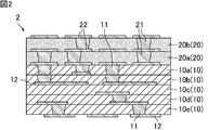
- FIG. 2 is a cross-sectional view schematically showing another example of the composite substrate of the present invention.
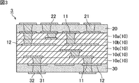
- FIG. 3 is a cross-sectional view schematically showing an example of a composite substrate on which a second resin insulating layer is arranged.
- FIG. 4 is a cross-sectional view schematically showing an example of a composite substrate in which a Cu post is used as a metal bulk.
- FIG. 1 is a cross-sectional view schematically showing an example of the composite substrate of the present invention.
- the composite substrate 1 of the present invention is a substrate comprising a ceramic layer 10 (10a, 10b, 10c, 10d, 10e) and a resin insulation layer 20 disposed on the surface of the ceramic layer 10.
- a ceramic material is present as an insulating material in the ceramic layer 10 and has a metal conductor 11 and a metal wiring 12 for interlayer connection.
- the resin insulating layer 20 has a resin material as an insulating material, and has a metal conductor 21 and a metal wiring 22 for interlayer connection.
- a part of the metal wiring 22 exposed on the surface of the resin insulating layer 20 may be an electrode for mounting an electronic component.
- the resin insulating layer 20 is formed directly on the surface of the ceramic layer 10, and no adhesive layer exists between the resin insulating layer 20 and the ceramic layer 10.
- the thermal expansion coefficient of the ceramic layer is 3 ppm / ° C. or higher and 30 ppm / ° C. or lower in the range of 30 ° C. to 400 ° C.
- the thermal expansion coefficient of the ceramic layer is preferably 5 ppm or more, and preferably 20 ppm or less.
- the thermal expansion coefficient of the ceramic layer is determined as the thermal expansion coefficient of the ceramic material constituting the ceramic layer.
- the thermal expansion coefficient of the ceramic material can be measured according to JIS R1618 (2002) “Measurement method of thermal expansion by thermomechanical analysis of fine ceramics”.
- the thermal expansion coefficient ⁇ (ppm / ° C) in the range of 30 ° C. to 400 ° C. is shown in parentheses
- alumina ⁇ 7.8 to 8 to 8) .1
- zirconia ⁇ 8.5 to 11.3
- silicon carbide ⁇ 4.4 to 4.6
- aluminum nitride ⁇ 4.4 to 5.4
- forsterite ⁇ 9.7
- ferrite ⁇ 9.5 to 14.5
- calcium titanate ⁇ 11.5)
- barium titanate ( ⁇ 9.6), and the like.
- the ceramic material is also preferably a low-temperature sintered ceramic material.
- Low-temperature sintered ceramic material is a material that can be sintered at a firing temperature of 1000 ° C. or less among ceramic materials and can be simultaneously fired with silver or copper, which is preferably used as a metal material constituting a metal conductor. Means.
- the low-temperature sintered ceramic material is a glass composite low-temperature sintered ceramic material obtained by mixing borosilicate glass with a ceramic material such as quartz, alumina, forsterite, or the like, ZnO—MgO—Al 2 O 3 — Crystallized glass-based low-temperature sintered ceramic materials using SiO 2 -based crystallized glass, BaO—Al 2 O 3 —SiO 2 ceramic materials and Al 2 O 3 —CaO—SiO 2 —MgO—B 2 O 3 systems
- a non-glass type low-temperature sintered ceramic material using a ceramic material or the like can be used. Among these, those having a thermal expansion coefficient in the range of 30 ° C. to 400 ° C.
- Al 2 O 3 —CaO—SiO 2 —MgO—B 2 O 3 ceramic material one having a thermal expansion coefficient of 5.5 ppm / ° C. or more and 7.2 ppm / ° C. or less can be preferably used.
- the resin insulating layer has a tensile elastic modulus of 3 GPa or less, preferably 1 GPa or less.
- the tensile elastic modulus of the resin insulating layer can be calculated using a test piece having a width of 25 mm and a length of 150 mm based on JIS K 7161.
- the tensile elastic modulus of the resin insulating layer is not the tensile elastic modulus of the resin material but the value of the tensile elastic modulus measured for the entire resin insulating layer.
- it is preferable that the tensile elasticity modulus of a resin insulating layer is 0.02 GPa or more.
- a fluorine resin As a resin material having a low tensile elastic modulus, a fluorine resin, a polyimide resin, a polyether ketone resin, a polyphenylene sulfide resin, a cycloolefin resin, or the like can be preferably used. More preferable specific examples include a fluorine-based resin having a tensile elastic modulus E (GPa) ⁇ 0.39 to 0.55, a cycloolefin resin having a tensile elastic modulus E (GPa) ⁇ 2.1 to 2.2, and the like. can do. Since these resin materials have low tensile elastic modulus, the resin insulating layer works effectively as a stress relaxation layer against impact.
- the board substrate with high reliability with respect to a drop impact and a thermal shock.
- materials such as rubber materials and thermoplastic elastomers (vinyl chloride, styrene, olefin, ester, urethane, amide, etc.) can also be used.
- the relative dielectric constant ⁇ r of the resin insulating layer is preferably 1.5 or more and 3 or less.
- a resin material for obtaining a preferable dielectric constant a fluorine-based resin, silicone rubber, or a hydrocarbon-based resin having a small polar group (for example, polyethylene, polypropylene, polystyrene, etc.) can be preferably used.
- Polypropylene having a dielectric constant of 2 and polystyrene having a dielectric constant ⁇ r ⁇ 2.45 can be used.
- the dielectric constant can be measured by measuring a sample having a size of 50 mm ⁇ 50 mm ⁇ 0.5 mmt at a frequency of 9 GHz using a perturbation method.
- the relative dielectric constant of the resin insulating layer is not the relative dielectric constant of the resin material but the value of the relative dielectric constant measured for the entire resin insulating layer.
- the thermal expansion coefficient of the resin insulating layer is not particularly limited. However, in the composite substrate of the present invention, it is not necessary to match the thermal expansion coefficient of the ceramic layer. It is not necessary to reduce the amount by adding, etc. Therefore, the thermal expansion coefficient of the resin insulating layer may be high, and is preferably 7 ppm / ° C. or higher in the range of 30 ° C. to 400 ° C. Moreover, it is also preferable that it is 20 ppm / degrees C or less.
- the thermal expansion coefficient of the resin insulating layer means the thermal expansion coefficient of the resin material constituting the resin insulating layer.
- the thermal expansion coefficient of the resin material is JIS K7197 (2012) “Linear expansion coefficient test by thermomechanical analysis of plastics. It can be measured according to “Method”.
- the ceramic layer and the resin insulating layer are provided with metal conductors and metal wirings for interlayer connection.
- Arbitrary conductor materials can be used as the metal conductor and the metal wiring.
- the material constituting the metal conductor in the ceramic layer is preferably Cu
- the metal material constituting the metal conductor in the resin insulating layer is a simple substance of Sn, Mn and Ni, and an alloy of Cu and Sn, Mn or Ni. It is preferably made of a material containing Cu and at least one metal selected from the group consisting of materials.
- the metal material constituting the metal conductor in the resin insulating layer is a material containing Sn alone and a Cu—Mn alloy and Cu, or a material containing Sn alone and a Cu—Ni alloy and Cu. It is more preferable that
- FIG. 2 is a cross-sectional view schematically showing another example of the composite substrate of the present invention.
- the composite substrate 2 shown in FIG. 2 has the same configuration as the composite substrate 1 shown in FIG. 1 except that the resin insulating layer 20 has a multilayer structure including a resin insulating layer 20a and a resin insulating layer 20b. Also in this case, the resin insulating layer 20 is formed directly on the surface of the ceramic layer 10, and no adhesive layer exists between the resin insulating layer 20 and the ceramic layer 10.
- the tensile elastic modulus of the resin insulating layer is determined for each layer. And even if one of the plurality of resin insulation layers has a resin insulation layer whose tensile elastic modulus is 3 GPa or less, it is included in the composite substrate of the present invention as the tensile elastic modulus of the resin insulation layer is 3 GPa or less. I will do it. This is because if there is only one resin insulating layer having a low tensile elastic modulus, the resin insulating layer can effectively function as a stress relaxation layer against impact.
- the resin insulating layer has a multilayer structure and each resin insulating layer has a different tensile elastic modulus
- a resin insulating layer having a lower tensile elastic modulus is formed on the surface of the ceramic layer.
- the tensile elasticity modulus of the resin insulating layer formed directly on the surface of the ceramic layer is 3 GPa or less.
- the simplest structure of the composite substrate of the present invention includes a composite substrate comprising one ceramic layer and one resin insulating layer disposed on the surface of the ceramic layer.
- 1 and 2 show an embodiment in which a resin insulating layer is arranged on one surface (upper surface) of the ceramic layer, but the other surface (lower surface) of the ceramic layer is shown.
- a resin insulating layer may be disposed.
- the resin insulating layer disposed on the other surface is preferably a second resin insulating layer having a tensile elastic modulus of 3 GPa or less.
- the second resin insulating layer is disposed with the upper surface of the ceramic layer as the first surface of the ceramic layer and the lower surface as the second surface of the ceramic layer. That is, in the composite substrate of the present invention, the second elastic modulus is 3 GPa or less on the second surface located on the opposite side to the first surface on which the resin insulating layer is disposed among the surfaces of the ceramic layer. It is preferable that the resin insulating layer is disposed.
- FIG. 3 is a cross-sectional view schematically showing an example of a composite substrate on which a second resin insulating layer is arranged.
- the second resin insulating layer 30 has a resin material as an insulating material, and has a metal conductor 31 and a metal wiring 32 for interlayer connection.
- the metal conductor 31 for interlayer connection is electrically connected to the metal wiring 12 of the ceramic layer 10.
- the second resin insulation layer 30 is also preferably formed directly on the second surface, which is the surface of the ceramic layer 10.
- the second resin insulation layer has a tensile modulus of 3 GPa or less.
- the resin material constituting the second resin insulation layer the same material as the resin material constituting the resin insulation layer described above can be preferably used, and the specific form of the second resin insulation layer is It can be the same as the resin insulating layer described above. Further, the resin material constituting the second resin insulation layer and the resin material constituting the resin insulation layer may be the same or different.
- the second resin insulation layer may have a single layer structure or a multilayer structure. When the second resin insulation layer has a multilayer structure, the form of the second resin insulation layer can be the same as the form of the resin insulation layer in the composite substrate 2 shown in FIG.
- the metal conductor in the resin insulating layer is a metal bulk made of Cu or an alloy containing Cu, and at least one of the upper surface side and the lower surface side is soldered.
- CuNi alloy etc. are mentioned as an alloy containing Cu.
- the metal bulk means a metal conductor made of a lump of metal, and examples include a metal post, a metal ball, and a metal block.
- the shape of the metal bulk can be a prismatic shape, a columnar shape, a spherical shape, or the like, and preferably has a height approximately the same as the resin insulating layer in which the metal bulk is disposed.
- the metal bulk is electrically connected to the metal wiring on the upper surface side and the lower surface side, but it is preferable that at least one of them is soldered to the metal wiring.
- FIG. 4 is a cross-sectional view schematically showing an example of a composite substrate in which a Cu post is used as a metal bulk.
- a plurality of Cu posts 40 are provided in the resin insulating layer 20a.
- the Cu post 40 is solder-joined with the metal wiring 12 on the lower surface side thereof and the solder 42, and is solder-joined with the metal wiring 22 on the upper surface side and the solder 43.
- FIG. 4 shows a view in which both the upper and lower surfaces of the Cu post are soldered, but only one surface of the upper and lower surfaces is soldered, and the other surface is a method other than soldering. It may be fixed with.
- the electronic components may be arranged side by side from the upper side and the lower side of the resin insulating layer.
- the electronic component 52 is disposed from the lower side of the resin insulating layer 20a, and the electronic component 53 is disposed from the upper side of the resin insulating layer 20a. With this arrangement, the space in the resin insulating layer can be used effectively.
- the electronic component 51 is a high electronic component, the thickness of the resin insulating layer 20a is determined so that the electronic component 51 can be inserted.
- the electronic components 51a are arranged on the resin insulating layer 20a.
- the space on the electronic component 52 and the space on the electronic component 53 are wasted if the electronic component 52 and the electronic component 53 are also arranged side by side below the resin insulating layer 20a. Become. Therefore, if the electronic component 52 and the electronic component 53 are arranged side by side from the upper side and the lower side of the resin insulating layer, the space in the resin insulating layer can be used effectively.
- a ceramic substrate comprising a ceramic layer having a thermal expansion coefficient in the range of 30 ° C. to 400 ° C. of 3 ppm / ° C. or more and 30 ppm / ° C. or less is prepared, and a tensile elastic modulus is provided on the surface of the ceramic substrate. It can manufacture by performing the process of directly sticking the resin film used as the resin insulation layer which is 3 GPa or less.
- the ceramic substrate can be produced by firing a ceramic green sheet. It is preferable to form a metal conductor for interlayer connection, a wiring pattern and an electrode before or after firing on the ceramic substrate.
- a low-temperature sintered ceramic material as the ceramic material, drill the ceramic green sheet, fill the hole with a metal conductor paste containing copper or silver, and fire the ceramic green sheet at a temperature at which the ceramic material sinters
- the ceramic material and the metal conductor paste can be sintered at a time to produce a ceramic substrate on which a metal conductor for interlayer connection is formed.
- a thermoplastic film is preferably used as the resin film, and the resin film can be directly attached to the surface of the ceramic substrate by stacking the resin film on the ceramic substrate and performing high-temperature pressure bonding.
- the conditions for high-temperature pressure bonding may be determined in accordance with the characteristics of the resin material constituting the resin film. It is preferable to perform the pressing under a condition of 12 MPa or less and a pressure bonding time of 1 minute or more and 120 minutes or less.
- the resin film is preferably a resin film that can be directly attached, and can be combined with a ceramic substrate by pressurization at a high temperature. When the adhesion strength is insufficient, an adhesive may be used to form a composite with the ceramic substrate.
- the resin film may be subjected to perforation and formation of a metal conductor for interlayer connection to the perforations before being attached. Further, a wiring pattern and electrodes may be formed on the surface of the resin film. In this case, since a plurality of resin films can be bonded together, the lead time can be shortened. Moreover, after affixing the resin film on the surface of the ceramic substrate, a hole may be formed in the resin film and a metal conductor for interlayer connection to the hole may be formed. In this case, the alignment accuracy can be increased. Further, a wiring pattern and electrodes may be formed on the surface of the resin film. These methods are not particularly limited, and metal conductor paste filling or plating can be used for forming the metal conductor. In addition, the wiring pattern can be formed by a technique such as a method of attaching and etching a copper foil or a screen printing using a metal conductor paste.
- a resin insulation layer can be further provided by a build-up method on the resin insulation layer of the composite substrate in which the resin insulation layer is provided on the surface of the ceramic layer.
- the second resin insulating layer In the case of manufacturing a composite substrate on which the second resin insulating layer as shown in FIG. 3 is manufactured, it is located on the opposite side of the surface of the ceramic layer from the first surface on which the resin insulating layer is arranged.
- the second resin insulating layer may be formed on the second surface in the same manner as the method for forming the resin insulating layer.
- a composite substrate having a resin insulating layer formed on the first surface is prepared, and a second resin insulating layer is formed by stacking a resin film on the second surface of the ceramic layer of the composite substrate and performing high-temperature pressure bonding. Can do.
- a resin insulating layer may be simultaneously formed on the first surface and the second surface of the ceramic substrate by stacking a resin film on each of the first surface and the second surface of the ceramic substrate and performing high-temperature pressure bonding. .
- the resin insulating layer formed on the second surface of the ceramic layer among the resin insulating layers formed simultaneously is regarded as the second resin insulating layer.
- a substrate in which a space of a predetermined height is formed using the metal bulk, and the resin serving as a material for the resin insulating layer is filled in the space.
- a resin insulating layer can be formed.
- the ceramic substrate formed up to the ceramic layer 10a and the Cu post 40 are formed to stand downward on the lower surface of the resin insulation layer 20b.
- the resin substrate and the ceramic substrate are combined with the Cu post 40 facing the ceramic layer 10a side.
- the Cu post 40 and the metal wiring 12 of the ceramic layer 10 a are joined by the solder 42.
- the arrangement of the electronic components when the Cu post 40 is soldered to the metal wiring 12 is shown in FIG.
- the arrangement is as shown below. Since a space is secured between the resin insulating layer 20b and the ceramic layer 10a by the Cu post 40, the resin insulating layer 20a is formed by filling this space with a liquid resin material such as silicone rubber. 4 can be manufactured.
- the Cu post may be provided on the ceramic layer side.
- a ceramic substrate with the Cu post 40 facing upward from the metal wiring 12 of the ceramic substrate on which the ceramic layer 10a is formed, and a resin insulating layer 20b with the metal wiring 22 formed on the surface are prepared. Then, the ceramic post and the resin substrate are combined with the Cu post 40 facing the resin insulating layer 20b. The Cu post 40 and the metal wiring 22 of the resin insulating layer 20 b are joined by the solder 43. If the electronic component 51 and the electronic component 52 are bonded to the ceramic substrate and the electronic component 53 is bonded to the resin substrate, the arrangement of the electronic components when the Cu post 40 is soldered to the metal wiring 22 is shown in FIG. The arrangement is as shown below. Since a space is secured between the resin insulating layer 20b and the ceramic layer 10a by the Cu post 40, the resin insulating layer 20a is formed by filling this space with a liquid resin material such as silicone rubber. 4 can be manufactured.
- a Ni plating film or an Au plating film may be formed on the electrode formed on the surface of the composite substrate. Furthermore, an electronic component or the like can be mounted on the electrode.
- Example 1 A Cu-based electrode was placed on the fired ceramic substrate produced by a normal green sheet process, and the resin film was bonded by high-temperature pressure bonding. Then, the resin film of the electrode part on a ceramic substrate was pierced, and after filling with a metal conductor paste, the Cu foil was hot-pressed at 300 ° C. Further, a wiring pattern was formed by Cu foil etching, and two resin insulation layers were formed by repeating this.
- a composite substrate was produced by the above method. As the ceramic substrate, a BaO—Al 2 O 3 —SiO 2 ceramic material was used, and the thermal expansion coefficient was 15 ppm / ° C. in the range of 30 ° C. to 400 ° C.
- the resin film As the resin film, a cycloolefin resin film having a tensile modulus of 1 GPa was used, and the thermal expansion coefficient was 150 ppm / ° C. in the range of 30 ° C. to 400 ° C.
- Example 2 A composite substrate was produced in the same manner as in Example 1 except that a fluororesin film having a tensile modulus of 0.1 GPa was used as the resin film.
- Example 3 A composite substrate was produced in the same manner as in Example 1 except that a polyimide resin film having a tensile modulus of 3 GPa was used as the resin film.
- Example 1 A composite substrate was produced in the same manner as in Example 1 except that a liquid crystal polymer film having a tensile modulus of 10 GPa was used as the resin film.
- Ceramic substrates having different thermal expansion coefficients were prepared, and the substrates of Comparative Examples 2 to 6 were used for the following evaluation without forming a resin insulating layer.
- Drop impact test A drop impact test was performed on the composite substrate and the ceramic substrate manufactured in each example and comparative example. The evaluation results are summarized in Table 1.
- the drop impact test was performed by a method based on JEDEC JESD22-B111. When 30 composite boards are solder-mounted on a test board so as to form a daisy chain circuit and dropped 300 times with an impact acceleration of 1500 G, 1.0 ms, and a sine half wave, and there is a failure such as disconnection or crack The case where there was no failure such as x, disconnection, crack, etc. was marked as ⁇ .
- Heat cycle test A heat cycle test was performed on the composite substrate and the ceramic substrate manufactured in each Example and Comparative Example. The evaluation results are summarized in Table 1. 30 composite boards are solder-mounted on a test board so as to form a daisy chain circuit, and a cycle of + 85 ° C. to ⁇ 40 ° C. and a holding time of 30 min is performed 400 times. The case where there was no failure such as a crack was rated as ⁇ .
- the substrate warpage amount was measured for the composite substrate and the ceramic substrate manufactured in each Example and Comparative Example.
- the evaluation results are summarized in Table 1.
- the height of 25 points in the substrate surface was measured with a laser, and the amount of warpage was calculated from the height difference.
- the tensile elastic modulus of the resin insulating layer is low, so that the surface unevenness is small, and the substrate is strong against temperature change and drop impact. It was.
- the resin insulating layer has a particularly low tensile elastic modulus, the amount of substrate warpage and surface unevenness were lower.
- the composite insulating substrate of Comparative Example 1 has a high tensile modulus of elasticity of the resin insulating layer, it is a substrate that is weak against temperature changes and drop impacts.
- the ceramic substrates of Comparative Examples 2 to 6 since the resin insulating layer was not disposed on the surface of the ceramic layer, the unevenness generated on the surface of the ceramic layer remained as it was, and the smoothness was poor.
- Example 4 On the surface (second surface of the ceramic substrate) on the side where the resin insulating layer is not disposed of the composite substrate of Example 2 prepared using a fluororesin film having a tensile modulus of 0.1 GPa as the resin film
- the fluororesin film used in Example 2 was joined by high-temperature pressure bonding in the same manner as described in the description of Example 1.
- the resin film of the electrode part on a ceramic substrate was pierced, and after filling with a metal conductor paste, the Cu foil was hot-pressed at 300 ° C.
- the wiring pattern was formed by Cu foil etching, and the 2nd resin insulation layer which consists of two layers was formed by repeating it.
- a composite substrate was produced by the above method.
- Example 5 A fluororesin film having a tensile elastic modulus of 0.1 GPa and a thermal expansion coefficient of 250 ppm / ° C. in the range of 30 ° C. to 400 ° C. was prepared as a resin film. Using this fluororesin film, a composite substrate having a resin insulating layer disposed on the surface of the ceramic substrate (the first surface of the ceramic substrate) was produced in the same manner as in Example 1. Further, the composite substrate is formed of two layers in the same manner as in Example 4 by using this fluororesin film on the surface on which the resin insulating layer is not disposed (second surface of the ceramic substrate). A second resin insulation layer was formed to produce a composite substrate.
Landscapes
- Engineering & Computer Science (AREA)
- Microelectronics & Electronic Packaging (AREA)
- Manufacturing & Machinery (AREA)
- Production Of Multi-Layered Print Wiring Board (AREA)
Abstract
本発明の複合基板は、セラミック層と、上記セラミック層の表面に配置された樹脂絶縁層とを有する複合基板であって、上記セラミック層の熱膨張係数は30℃~400℃の範囲で3ppm/℃以上、30ppm/℃以下であり、上記樹脂絶縁層の引っ張り弾性率が3GPa以下であることを特徴とする。
Description
本発明は、複合基板及び複合基板の製造方法に関する。
スマートフォンなどのモバイル向け通信モジュール用基板は小型化・低背化が要求される中で、より小型で狭ピッチバンプを有するIC実装などの技術が採用され、平坦性や電極位置精度において高い品質の多層配線基板が求められている。
特に高精度が求められる半導体パッケージ基板に対しては実装およびリフロー時の反りや変形などが生じにくく、形状安定性の高いコア基板上に薄膜ビルドアップ層を形成することにより高精度で微細な配線層を形成している。
特に高精度が求められる半導体パッケージ基板に対しては実装およびリフロー時の反りや変形などが生じにくく、形状安定性の高いコア基板上に薄膜ビルドアップ層を形成することにより高精度で微細な配線層を形成している。
特許文献1には、セラミック基板からなるコア基板の上に薄膜ビルドアップ層等の樹脂絶縁層が設けられた多層配線基板が開示されており、電極がない部分の樹脂絶縁層を部分的に厚くすることで、IC実装面を平坦化している。
特許文献1のようにコア基板と樹脂絶縁層が設けられた多層配線基板において、樹脂絶縁層に熱膨張係数の高いポリイミドやエポキシ系などの一般的な樹脂材料を適用する場合には、使用時などに大きな温度変動が生じると熱膨張係数差による応力によりビア部分で破断するリスクがある。
そのため、樹脂絶縁層に無機フィラーなどを多量に添加することで樹脂材料の熱膨張係数を低下させることが考えられる。しかし、無機フィラーを多量に添加すると孔開け加工性が低下したり、誘電率が高くなることで高周波特性が劣化するなどのデメリットがある。
そのため、樹脂材料を、その熱膨張係数を低下させることなく熱膨張係数の高いままで樹脂絶縁層として適用する技術が必要になっている。
さらに、モバイル機器で用いるようなモジュール基板においては、温度変動以外にも落下衝撃などのリスクもあり、特に強度面での信頼性が問題となる。
なお、樹脂絶縁層を用いずにセラミック基板だけの基板とすると、厚み方向の焼成収縮による表面平坦性が問題となり、部品実装精度が低下するという問題がある。
そのため、樹脂絶縁層に無機フィラーなどを多量に添加することで樹脂材料の熱膨張係数を低下させることが考えられる。しかし、無機フィラーを多量に添加すると孔開け加工性が低下したり、誘電率が高くなることで高周波特性が劣化するなどのデメリットがある。
そのため、樹脂材料を、その熱膨張係数を低下させることなく熱膨張係数の高いままで樹脂絶縁層として適用する技術が必要になっている。
さらに、モバイル機器で用いるようなモジュール基板においては、温度変動以外にも落下衝撃などのリスクもあり、特に強度面での信頼性が問題となる。
なお、樹脂絶縁層を用いずにセラミック基板だけの基板とすると、厚み方向の焼成収縮による表面平坦性が問題となり、部品実装精度が低下するという問題がある。
本発明は上記の課題を解決するためになされたものであり、セラミック層の表面に樹脂絶縁層を形成した場合でも、温度変化や落下衝撃に対する信頼性が高い複合基板を提供することを目的とする。
上記目的を達成するための、本発明の複合基板は、セラミック層と、上記セラミック層の表面に配置された樹脂絶縁層とを有する複合基板であって、上記セラミック層の熱膨張係数は30℃~400℃の範囲で3ppm/℃以上、30ppm/℃以下であり、上記樹脂絶縁層の引っ張り弾性率が3GPa以下であることを特徴とする。
本発明の複合基板では、セラミック層の熱膨張係数が3ppm/℃以上、30ppm/℃以下であり、セラミック層として熱膨張係数が低いものを使用することができる。セラミック層として熱膨張係数が特に高いものを使用する必要はない。
そして、樹脂絶縁層がセラミック層の表面に配置されているためにセラミック層の表面に生じる凹凸を緩和して表面の平滑性の高い複合基板とすることができる。
また、樹脂絶縁層の引っ張り弾性率が3GPa以下となっている。引っ張り弾性率が3GPa以下であると樹脂絶縁層が柔らかく、樹脂絶縁層が衝撃に対する応力緩和層として有効に働く。そのため、落下衝撃及び熱衝撃に対する信頼性が高い基板とすることができる。
そして、樹脂絶縁層がセラミック層の表面に配置されているためにセラミック層の表面に生じる凹凸を緩和して表面の平滑性の高い複合基板とすることができる。
また、樹脂絶縁層の引っ張り弾性率が3GPa以下となっている。引っ張り弾性率が3GPa以下であると樹脂絶縁層が柔らかく、樹脂絶縁層が衝撃に対する応力緩和層として有効に働く。そのため、落下衝撃及び熱衝撃に対する信頼性が高い基板とすることができる。
本発明の複合基板では、上記樹脂絶縁層が上記セラミック層の表面に直接形成されていることが好ましい。本発明の複合基板では樹脂絶縁層の引っ張り弾性率が3GPa以下となる柔らかい樹脂材料を使用しており、このような柔らかい樹脂材料には接着材を介することなくセラミック層と直接接着できる性質を有するものがある。接着材を介することなくセラミック層の表面に樹脂絶縁層が直接形成されていると簡便な構成の複合基板とすることができ、製造工程も簡便にすることができるので好ましい。
本発明の複合基板では、上記樹脂絶縁層の比誘電率εrが1.5以上3以下であることが好ましい。樹脂絶縁層の比誘電率εrが1.5以上3以下であると、高周波領域での伝送損失を低減することに適した基板とすることができる。また、フィルター回路などの機能を内蔵させることが可能である。
本発明の複合基板では、上記セラミック層及び上記樹脂絶縁層にはそれぞれ層間接続用の金属導体が設けられており、上記セラミック層における金属導体を構成する金属材料はCuであり、上記樹脂絶縁層における金属導体を構成する金属材料は、Sn、Mn及びNiの単体並びにCuとSn、Mn又はNiとの合金材料からなる群から選択された少なくとも1種の金属と、Cuとを含む材料からなることが好ましい。
樹脂絶縁層における金属導体を構成する金属材料は、融点変動型の金属材料であり、加熱して融解させ、冷却して固化させた後に融点が高くなる材料である。
このような材料を樹脂絶縁層の金属導体の材料として使用すると、セラミック層の金属導体に対して接合させるときは融点が低いため比較的低温での信頼性が高い接合を形成することができる。また、接合後に融点が高くなるので樹脂絶縁層を複数層ビルドアップにより積み上げていく際の加熱では再溶融が生じないので樹脂絶縁層を複数層形成することが容易になる。
樹脂絶縁層における金属導体を構成する金属材料は、融点変動型の金属材料であり、加熱して融解させ、冷却して固化させた後に融点が高くなる材料である。
このような材料を樹脂絶縁層の金属導体の材料として使用すると、セラミック層の金属導体に対して接合させるときは融点が低いため比較的低温での信頼性が高い接合を形成することができる。また、接合後に融点が高くなるので樹脂絶縁層を複数層ビルドアップにより積み上げていく際の加熱では再溶融が生じないので樹脂絶縁層を複数層形成することが容易になる。
本発明の複合基板では、上記樹脂絶縁層における層間接続用の金属導体は、Cu又はCuを含む合金(例えば、CuNi合金)からなる金属バルクであり、その上面側及び下面側の少なくとも一方がはんだ接合されていることが好ましい。
樹脂絶縁層に設ける金属導体が金属バルクであり、それがはんだ接合されていると、熱衝撃に対する接続信頼性に優れる。
また、金属バルクを先に形成することによって空間を設け、その空間に樹脂を流すことによって樹脂絶縁層を形成させることができる。このような樹脂絶縁層の形成方法の場合、空間に電子部品を配置してから樹脂絶縁層の形成を行うことができ、樹脂絶縁層内における電子部品の配置の位置の自由度が向上する。
樹脂絶縁層に設ける金属導体が金属バルクであり、それがはんだ接合されていると、熱衝撃に対する接続信頼性に優れる。
また、金属バルクを先に形成することによって空間を設け、その空間に樹脂を流すことによって樹脂絶縁層を形成させることができる。このような樹脂絶縁層の形成方法の場合、空間に電子部品を配置してから樹脂絶縁層の形成を行うことができ、樹脂絶縁層内における電子部品の配置の位置の自由度が向上する。
本発明の複合基板では、上記セラミック層の表面のうち上記樹脂絶縁層が配置された第1の表面とは反対側に位置する第2の表面に、引っ張り弾性率が3GPa以下である第2の樹脂絶縁層が配置されていることが好ましい。
セラミック層の両方の表面に樹脂絶縁層が配置されていると、リフローといった熱サイクル負荷がかかる工程などで、セラミック層と樹脂絶縁層の熱膨張係数の差により発生するセラミック層の反り(たわみ)を抑制することができる。そのため、複合基板への部品実装等の後工程におけるハンドリング性を向上させることができる。また、ビア接続面などの商品信頼性を向上させることができる。
セラミック層の両方の表面に樹脂絶縁層が配置されていると、リフローといった熱サイクル負荷がかかる工程などで、セラミック層と樹脂絶縁層の熱膨張係数の差により発生するセラミック層の反り(たわみ)を抑制することができる。そのため、複合基板への部品実装等の後工程におけるハンドリング性を向上させることができる。また、ビア接続面などの商品信頼性を向上させることができる。
本発明の複合基板の製造方法は、熱膨張係数が30℃~400℃の範囲で3ppm/℃以上、30ppm/℃以下であるセラミック層からなるセラミック基板の表面に、引っ張り弾性率が3GPa以下である樹脂絶縁層となる樹脂フィルムを直接貼り付ける工程を行うことを特徴とする。
上記工程では、接着材を介することなくセラミック層の表面に樹脂絶縁層を直接形成することができる。接着材をセラミック層又は樹脂フィルムに塗布する必要が無く、製造工程を簡略化することができるので好ましい。
上記工程では、接着材を介することなくセラミック層の表面に樹脂絶縁層を直接形成することができる。接着材をセラミック層又は樹脂フィルムに塗布する必要が無く、製造工程を簡略化することができるので好ましい。
本発明の複合基板の製造方法では、上記セラミック基板の表面に上記樹脂フィルムを直接貼り付ける工程の後に、上記樹脂フィルムへの孔開け及び孔に対する層間接続用の金属導体の形成を行うことが好ましい。
また、本発明の複合基板の製造方法では、上記樹脂フィルムへの孔開け及び孔に対する層間接続用の金属導体の形成を行った後に、上記セラミック基板の表面に上記樹脂フィルムを直接貼り付ける工程を行うことも好ましい。
すなわち、樹脂絶縁層に層間接続用の金属導体を設ける際に、樹脂フィルムをセラミック基板に貼り付けた後に金属導体の形成を行ってもよいし、予め金属導体を形成した樹脂フィルムをセラミック基板に貼り付けてもよい。
また、本発明の複合基板の製造方法では、上記樹脂フィルムへの孔開け及び孔に対する層間接続用の金属導体の形成を行った後に、上記セラミック基板の表面に上記樹脂フィルムを直接貼り付ける工程を行うことも好ましい。
すなわち、樹脂絶縁層に層間接続用の金属導体を設ける際に、樹脂フィルムをセラミック基板に貼り付けた後に金属導体の形成を行ってもよいし、予め金属導体を形成した樹脂フィルムをセラミック基板に貼り付けてもよい。
この発明によれば、セラミック層の表面に樹脂絶縁層を形成した場合でも、温度変化や落下衝撃に対する信頼性が高い複合基板を提供することができる。
以下、本発明の複合基板及びその製造方法について説明する。
しかしながら、本発明は、以下の構成に限定されるものではなく、本発明の要旨を変更しない範囲において適宜変更して適用することができる。
以下に示す各実施形態は例示であり、異なる実施形態で示した構成の部分的な置換又は組み合わせが可能であることは言うまでもない。
以下において記載する本発明の個々の好ましい構成を2つ以上組み合わせたものもまた本発明である。
しかしながら、本発明は、以下の構成に限定されるものではなく、本発明の要旨を変更しない範囲において適宜変更して適用することができる。
以下に示す各実施形態は例示であり、異なる実施形態で示した構成の部分的な置換又は組み合わせが可能であることは言うまでもない。
以下において記載する本発明の個々の好ましい構成を2つ以上組み合わせたものもまた本発明である。
<複合基板>
まず、複合基板の構成の一例について説明する。
図1は、本発明の複合基板の一例を模式的に示す断面図である。
本発明の複合基板1は、セラミック層10(10a、10b、10c、10d、10e)と、セラミック層10の表面に配置された樹脂絶縁層20とからなる基板である。
セラミック層10にはセラミック材料が絶縁材料として存在し、層間接続用の金属導体11及び金属配線12を有している。また、樹脂絶縁層20には樹脂材料が絶縁材料として存在し、層間接続用の金属導体21及び金属配線22を有している。樹脂絶縁層20の表面に露出している金属配線22の一部は電子部品を搭載するための電極であってもよい。
樹脂絶縁層20はセラミック層10の表面に直接形成されており、樹脂絶縁層20とセラミック層10の間に接着材層は存在していない。
まず、複合基板の構成の一例について説明する。
図1は、本発明の複合基板の一例を模式的に示す断面図である。
本発明の複合基板1は、セラミック層10(10a、10b、10c、10d、10e)と、セラミック層10の表面に配置された樹脂絶縁層20とからなる基板である。
セラミック層10にはセラミック材料が絶縁材料として存在し、層間接続用の金属導体11及び金属配線12を有している。また、樹脂絶縁層20には樹脂材料が絶縁材料として存在し、層間接続用の金属導体21及び金属配線22を有している。樹脂絶縁層20の表面に露出している金属配線22の一部は電子部品を搭載するための電極であってもよい。
樹脂絶縁層20はセラミック層10の表面に直接形成されており、樹脂絶縁層20とセラミック層10の間に接着材層は存在していない。
セラミック層の熱膨張係数は30℃~400℃の範囲で3ppm/℃以上、30ppm/℃以下である。セラミック層の熱膨張係数は5ppm以上であることが好ましく、20ppm以下であることが好ましい。
セラミック層の熱膨張係数は、セラミック層を構成するセラミック材料の熱膨張係数として定める。セラミック材料の熱膨張係数は、JIS R1618(2002)「ファインセラミックスの熱機械分析による熱膨張の測定方法」に準拠して測定することができる。
セラミック層の熱膨張係数は、セラミック層を構成するセラミック材料の熱膨張係数として定める。セラミック材料の熱膨張係数は、JIS R1618(2002)「ファインセラミックスの熱機械分析による熱膨張の測定方法」に準拠して測定することができる。
このような熱膨張係数の範囲内にあるセラミック材料(括弧内に30℃~400℃の範囲での熱膨張係数α(ppm/℃)を示す)としては、アルミナ(α≒7.8~8.1)、ジルコニア(α≒8.5~11.3)、炭化ケイ素(α≒4.4~4.6)、窒化アルミニウム(α≒4.4~5.4)、フォルステライト(α≒9.7)、フェライト(α≒9.5~14.5)、チタン酸カルシウム(α≒11.5)、チタン酸バリウム(α≒9.6)等が挙げられる。
また、セラミック材料は、低温焼結セラミック材料であることも好ましい。
低温焼結セラミック材料とは、セラミック材料のうち、1000℃以下の焼成温度で焼結可能であり、金属導体を構成する金属材料として好ましく使用される銀や銅との同時焼成が可能である材料を意味する。
低温焼結セラミック材料とは、セラミック材料のうち、1000℃以下の焼成温度で焼結可能であり、金属導体を構成する金属材料として好ましく使用される銀や銅との同時焼成が可能である材料を意味する。
低温焼結セラミック材料としては、具体的には、クオーツやアルミナ、フォルステライト等のセラミック材料にホウ珪酸ガラスを混合してなるガラス複合系低温焼結セラミック材料、ZnO-MgO-Al2O3-SiO2系の結晶化ガラスを用いた結晶化ガラス系低温焼結セラミック材料、BaO-Al2O3-SiO2系セラミック材料やAl2O3-CaO-SiO2-MgO-B2O3系セラミック材料等を用いた非ガラス系低温焼結セラミック材料等を用いることができる。これらのうち、熱膨張係数が30℃~400℃の範囲で3ppm/℃以上、30ppm/℃以下のものを使用することができる。
例えば、Al2O3-CaO-SiO2-MgO-B2O3系セラミック材料として、熱膨張係数が5.5ppm/℃以上、7.2ppm/℃以下のものを好ましく使用することができる。
例えば、Al2O3-CaO-SiO2-MgO-B2O3系セラミック材料として、熱膨張係数が5.5ppm/℃以上、7.2ppm/℃以下のものを好ましく使用することができる。
樹脂絶縁層は、引っ張り弾性率が3GPa以下であり、好ましくは1GPa以下である。
樹脂絶縁層の引っ張り弾性率は、JIS K 7161に基づき、幅25mm×長さ150mmの試験片を用いて算出することができる。
樹脂絶縁層の引っ張り弾性率は樹脂材料の引っ張り弾性率ではなく、樹脂絶縁層全体として測定した引っ張り弾性率の値である。
また、樹脂絶縁層の引っ張り弾性率が0.02GPa以上であることが好ましい。
樹脂絶縁層の引っ張り弾性率は、JIS K 7161に基づき、幅25mm×長さ150mmの試験片を用いて算出することができる。
樹脂絶縁層の引っ張り弾性率は樹脂材料の引っ張り弾性率ではなく、樹脂絶縁層全体として測定した引っ張り弾性率の値である。
また、樹脂絶縁層の引っ張り弾性率が0.02GPa以上であることが好ましい。
引っ張り弾性率の低い樹脂材料として、フッ素系樹脂、ポリイミド系樹脂、ポリエーテルケトン系樹脂、ポリフェニレンスルフィド系樹脂、シクロオレフィン系樹脂等を好ましく使用することができる。
より好ましい具体例としては、引っ張り弾性率E(GPa)≒0.39~0.55のフッ素系樹脂、引っ張り弾性率E(GPa)≒2.1~2.2のシクロオレフィン系樹脂等を使用することができる。
これらの樹脂材料は引っ張り弾性率が低いため、樹脂絶縁層が衝撃に対する応力緩和層として有効に働く。そのため、落下衝撃及び熱衝撃に対する信頼性が高い基板とすることができる。
また、ゴム系材料、熱可塑性エラストマー(塩ビ系、スチレン系、オレフィン系、エステル系、ウレタン系、アミド系等)等の材料を使用することもできる。
より好ましい具体例としては、引っ張り弾性率E(GPa)≒0.39~0.55のフッ素系樹脂、引っ張り弾性率E(GPa)≒2.1~2.2のシクロオレフィン系樹脂等を使用することができる。
これらの樹脂材料は引っ張り弾性率が低いため、樹脂絶縁層が衝撃に対する応力緩和層として有効に働く。そのため、落下衝撃及び熱衝撃に対する信頼性が高い基板とすることができる。
また、ゴム系材料、熱可塑性エラストマー(塩ビ系、スチレン系、オレフィン系、エステル系、ウレタン系、アミド系等)等の材料を使用することもできる。
また、樹脂絶縁層の比誘電率εrが1.5以上3以下であることが好ましい。
例えば、好ましい比誘電率を得るための樹脂材料として、フッ素系樹脂、シリコーンゴム、極性基の少ない炭化水素系樹脂(例えばポリエチレン、ポリプロピレン、ポリスチレン等)を好ましく使用することができる。より好ましい具体例としては、誘電率εr≒2.6のフッ素系樹脂、誘電率εr≒3.0のシリコーンゴム、誘電率εr≒2.25のポリエチレン、誘電率εr≒2.2のポリプロピレン、誘電率εr≒2.45のポリスチレン等を使用することができる。
誘電率の測定は、摂動法を用いて、50mm×50mm×0.5mmtの大きさのサンプルを周波数9GHzで測定することにより行うことができる。
樹脂絶縁層の比誘電率は樹脂材料の比誘電率ではなく、樹脂絶縁層全体として測定した比誘電率の値である。
例えば、好ましい比誘電率を得るための樹脂材料として、フッ素系樹脂、シリコーンゴム、極性基の少ない炭化水素系樹脂(例えばポリエチレン、ポリプロピレン、ポリスチレン等)を好ましく使用することができる。より好ましい具体例としては、誘電率εr≒2.6のフッ素系樹脂、誘電率εr≒3.0のシリコーンゴム、誘電率εr≒2.25のポリエチレン、誘電率εr≒2.2のポリプロピレン、誘電率εr≒2.45のポリスチレン等を使用することができる。
誘電率の測定は、摂動法を用いて、50mm×50mm×0.5mmtの大きさのサンプルを周波数9GHzで測定することにより行うことができる。
樹脂絶縁層の比誘電率は樹脂材料の比誘電率ではなく、樹脂絶縁層全体として測定した比誘電率の値である。
また、樹脂絶縁層の熱膨張係数は特に限定されるものではないが、本発明の複合基板ではセラミック層の熱膨張係数との整合を図る必要はなく、樹脂絶縁層の熱膨張係数を無機フィラーの添加等により低下させる必要はない。そのため、樹脂絶縁層の熱膨脹係数は高くてもよく、30℃~400℃の範囲で7ppm/℃以上であることが好ましい。また、20ppm/℃以下であることも好ましい。
樹脂絶縁層の熱膨張係数は樹脂絶縁層を構成する樹脂材料の熱膨張係数を意味しており、樹脂材料の熱膨張係数は、JIS K7197(2012)「プラスチックの熱機械分析による線膨脹率試験方法」に準拠して測定することができる。
樹脂絶縁層の熱膨張係数は樹脂絶縁層を構成する樹脂材料の熱膨張係数を意味しており、樹脂材料の熱膨張係数は、JIS K7197(2012)「プラスチックの熱機械分析による線膨脹率試験方法」に準拠して測定することができる。
セラミック層及び樹脂絶縁層には層間接続用の金属導体と金属配線がそれぞれ設けられている。金属導体及び金属配線としては任意の導体材料を使用することができる。
特に、セラミック層における金属導体を構成する材料はCuであることが好ましく、樹脂絶縁層における金属導体を構成する金属材料は、Sn、Mn及びNiの単体並びにCuとSn、Mn又はNiとの合金材料からなる群から選択された少なくとも1種の金属と、Cuとを含む材料からなることが好ましい。
より具体的には、樹脂絶縁層における金属導体を構成する金属材料は、Snの単体及びCu-Mn合金とCuとを含む材料、又は、Snの単体及びCu-Ni合金とCuとを含む材料であることがより好ましい。
特に、セラミック層における金属導体を構成する材料はCuであることが好ましく、樹脂絶縁層における金属導体を構成する金属材料は、Sn、Mn及びNiの単体並びにCuとSn、Mn又はNiとの合金材料からなる群から選択された少なくとも1種の金属と、Cuとを含む材料からなることが好ましい。
より具体的には、樹脂絶縁層における金属導体を構成する金属材料は、Snの単体及びCu-Mn合金とCuとを含む材料、又は、Snの単体及びCu-Ni合金とCuとを含む材料であることがより好ましい。
図2は、本発明の複合基板の他の一例を模式的に示す断面図である。
図2に示す複合基板2は、樹脂絶縁層20が樹脂絶縁層20a及び樹脂絶縁層20bからなる多層構造となっている他は図1に示す複合基板1と同様の構成を有している。この場合も、樹脂絶縁層20はセラミック層10の表面に直接形成されており、樹脂絶縁層20とセラミック層10の間に接着材層は存在していない。
図2に示す複合基板2は、樹脂絶縁層20が樹脂絶縁層20a及び樹脂絶縁層20bからなる多層構造となっている他は図1に示す複合基板1と同様の構成を有している。この場合も、樹脂絶縁層20はセラミック層10の表面に直接形成されており、樹脂絶縁層20とセラミック層10の間に接着材層は存在していない。
樹脂絶縁層が多層構造となっている場合、樹脂絶縁層の引っ張り弾性率は1層ごとに定める。そして、複数ある樹脂絶縁層のうち1層でもその引っ張り弾性率が3GPa以下となっている樹脂絶縁層があれば樹脂絶縁層の引っ張り弾性率が3GPa以下であるとして本発明の複合基板に含まれることとする。
引っ張り弾性率が低い樹脂絶縁層が1層でもあればその樹脂絶縁層が衝撃に対する応力緩和層として有効に働くことができるためである。
また、樹脂絶縁層が多層構造となっていて、各樹脂絶縁層の引っ張り弾性率が異なる場合、引っ張り弾性率がより低い樹脂絶縁層がセラミック層の表面に形成されていることが好ましい。そして、セラミック層の表面に形成されている直接形成されている樹脂絶縁層の引っ張り弾性率が3GPa以下であることが好ましい。
引っ張り弾性率が低い樹脂絶縁層が1層でもあればその樹脂絶縁層が衝撃に対する応力緩和層として有効に働くことができるためである。
また、樹脂絶縁層が多層構造となっていて、各樹脂絶縁層の引っ張り弾性率が異なる場合、引っ張り弾性率がより低い樹脂絶縁層がセラミック層の表面に形成されていることが好ましい。そして、セラミック層の表面に形成されている直接形成されている樹脂絶縁層の引っ張り弾性率が3GPa以下であることが好ましい。
図1及び図2には、セラミック層が多層となっている実施形態例を示したが、セラミック層は多層でなくてもよく1層であってもよい。本発明の複合基板として最も単純な構成としては1層のセラミック層とそのセラミック層の表面に配置された1層の樹脂絶縁層からなる複合基板が挙げられる。
また、図1及び図2にはセラミック層の一方の表面(上側の表面)に樹脂絶縁層が配置された実施形態例を示したが、セラミック層のもう一方の表面(下側の表面)にも樹脂絶縁層が配置されていてもよい。
上記もう一方の表面に配置される樹脂絶縁層は、引っ張り弾性率が3GPa以下である第2の樹脂絶縁層であることが好ましい。
以下、セラミック層の上側の表面をセラミック層の第1の表面、下側の表面をセラミック層の第2の表面として、第2の樹脂絶縁層が配置された形態について説明する。
すなわち、本発明の複合基板においては、セラミック層の表面のうち樹脂絶縁層が配置された第1の表面とは反対側に位置する第2の表面に、引っ張り弾性率が3GPa以下である第2の樹脂絶縁層が配置されていることが好ましい。
また、図1及び図2にはセラミック層の一方の表面(上側の表面)に樹脂絶縁層が配置された実施形態例を示したが、セラミック層のもう一方の表面(下側の表面)にも樹脂絶縁層が配置されていてもよい。
上記もう一方の表面に配置される樹脂絶縁層は、引っ張り弾性率が3GPa以下である第2の樹脂絶縁層であることが好ましい。
以下、セラミック層の上側の表面をセラミック層の第1の表面、下側の表面をセラミック層の第2の表面として、第2の樹脂絶縁層が配置された形態について説明する。
すなわち、本発明の複合基板においては、セラミック層の表面のうち樹脂絶縁層が配置された第1の表面とは反対側に位置する第2の表面に、引っ張り弾性率が3GPa以下である第2の樹脂絶縁層が配置されていることが好ましい。
図3は、第2の樹脂絶縁層が配置された複合基板の一例を模式的に示す断面図である。
図3に示す複合基板3では、図1に示す複合基板1のセラミック層10の表面のうち、樹脂絶縁層20が配置された第1の表面と反対側に位置する第2の表面に、第2の樹脂絶縁層30が配置されている。
第2の樹脂絶縁層30には樹脂材料が絶縁材料として存在し、層間接続用の金属導体31及び金属配線32を有している。
層間接続用の金属導体31はセラミック層10の金属配線12と電気的に接続されている。
第2の樹脂絶縁層30も、セラミック層10の表面である第2の表面に直接形成されていることが好ましい。
図3に示す複合基板3では、図1に示す複合基板1のセラミック層10の表面のうち、樹脂絶縁層20が配置された第1の表面と反対側に位置する第2の表面に、第2の樹脂絶縁層30が配置されている。
第2の樹脂絶縁層30には樹脂材料が絶縁材料として存在し、層間接続用の金属導体31及び金属配線32を有している。
層間接続用の金属導体31はセラミック層10の金属配線12と電気的に接続されている。
第2の樹脂絶縁層30も、セラミック層10の表面である第2の表面に直接形成されていることが好ましい。
第2の樹脂絶縁層は、引っ張り弾性率が3GPa以下である。
第2の樹脂絶縁層を構成する樹脂材料としては、先に説明した樹脂絶縁層を構成する樹脂材料と同様の材料を好ましく使用することができ、第2の樹脂絶縁層の具体的な形態は先に説明した樹脂絶縁層と同様にすることができる。
また、第2の樹脂絶縁層を構成する樹脂材料と樹脂絶縁層を構成する樹脂材料は、同じであってもよく異なっていてもよい。
第2の樹脂絶縁層は、単層構造でも多層構造であってもよい。第2の樹脂絶縁層が多層構造である場合の第2の樹脂絶縁層の形態は、図2に示す複合基板2における樹脂絶縁層の形態と同様にすることができる。
第2の樹脂絶縁層を構成する樹脂材料としては、先に説明した樹脂絶縁層を構成する樹脂材料と同様の材料を好ましく使用することができ、第2の樹脂絶縁層の具体的な形態は先に説明した樹脂絶縁層と同様にすることができる。
また、第2の樹脂絶縁層を構成する樹脂材料と樹脂絶縁層を構成する樹脂材料は、同じであってもよく異なっていてもよい。
第2の樹脂絶縁層は、単層構造でも多層構造であってもよい。第2の樹脂絶縁層が多層構造である場合の第2の樹脂絶縁層の形態は、図2に示す複合基板2における樹脂絶縁層の形態と同様にすることができる。
また、樹脂絶縁層における金属導体が、Cu又はCuを含む合金からなる金属バルクであり、その上面側及び下面側の少なくとも一方がはんだ接合されていることも好ましい。
Cuを含む合金としては、CuNi合金等が挙げられる。
金属バルクとは、金属の塊からなる金属導体を意味しており、金属ポスト、金属ボール、金属ブロック等が挙げられる。金属バルクの形状は角柱状、円柱状、球状等にすることができ、金属バルクが配置される樹脂絶縁層とほぼ同じ程度の高さを有することが好ましい。
金属バルクは、その上面側及び下面側で金属配線と電気的に接続されるが、少なくとも一方が金属配線とはんだ接合されていることが好ましい。
Cuを含む合金としては、CuNi合金等が挙げられる。
金属バルクとは、金属の塊からなる金属導体を意味しており、金属ポスト、金属ボール、金属ブロック等が挙げられる。金属バルクの形状は角柱状、円柱状、球状等にすることができ、金属バルクが配置される樹脂絶縁層とほぼ同じ程度の高さを有することが好ましい。
金属バルクは、その上面側及び下面側で金属配線と電気的に接続されるが、少なくとも一方が金属配線とはんだ接合されていることが好ましい。
樹脂絶縁層において金属バルクにより確保された空間には、電子部品を配置することができる。
図4は、金属バルクとしてCuポストが使用された複合基板の一例を模式的に示す断面図である。
複合基板4では、樹脂絶縁層20a内にCuポスト40が複数設けられている。Cuポスト40はその下面側の金属配線12とはんだ42ではんだ接合され、上面側の金属配線22とはんだ43ではんだ接合されている。図4にはCuポストの上面と下面が両方ともはんだ接合されている図を示しているが、上面と下面のうち一方の面だけがはんだ接合されていて、他方の面がはんだ接合以外の方法で固定されていてもよい。
Cuポスト40により樹脂絶縁層20aの高さが確保されるので、樹脂絶縁層20aの中には電子部品(電子部品51、52、53)を配置することができる。樹脂絶縁層に配置する電子部品の種類は特に限定されるものではなく、IC、コンデンサ、インダクタ、抵抗、フィルター等を配置することができる。
図4は、金属バルクとしてCuポストが使用された複合基板の一例を模式的に示す断面図である。
複合基板4では、樹脂絶縁層20a内にCuポスト40が複数設けられている。Cuポスト40はその下面側の金属配線12とはんだ42ではんだ接合され、上面側の金属配線22とはんだ43ではんだ接合されている。図4にはCuポストの上面と下面が両方ともはんだ接合されている図を示しているが、上面と下面のうち一方の面だけがはんだ接合されていて、他方の面がはんだ接合以外の方法で固定されていてもよい。
Cuポスト40により樹脂絶縁層20aの高さが確保されるので、樹脂絶縁層20aの中には電子部品(電子部品51、52、53)を配置することができる。樹脂絶縁層に配置する電子部品の種類は特に限定されるものではなく、IC、コンデンサ、インダクタ、抵抗、フィルター等を配置することができる。
電子部品は、樹脂絶縁層の上側及び下側から並べて配置してもよい。電子部品52は樹脂絶縁層20aの下側から、電子部品53は樹脂絶縁層20aの上側から配置されており、このように配置することによって樹脂絶縁層内の空間を有効に使うことができる。
図4に示す例では、電子部品51が高さの高い電子部品であるため樹脂絶縁層20aの厚さはこの電子部品51が入るように決まるが、その他に樹脂絶縁層20aに配置される電子部品52や電子部品53の厚さがそれほど厚くない場合、電子部品52及び電子部品53も樹脂絶縁層の20aの下側に並べて配置すると電子部品52上の空間及び電子部品53上の空間が無駄になってしまう。そこで、電子部品52及び電子部品53を樹脂絶縁層の上側及び下側から並べて配置すると樹脂絶縁層内の空間を有効に使うことができる。
図4に示す例では、電子部品51が高さの高い電子部品であるため樹脂絶縁層20aの厚さはこの電子部品51が入るように決まるが、その他に樹脂絶縁層20aに配置される電子部品52や電子部品53の厚さがそれほど厚くない場合、電子部品52及び電子部品53も樹脂絶縁層の20aの下側に並べて配置すると電子部品52上の空間及び電子部品53上の空間が無駄になってしまう。そこで、電子部品52及び電子部品53を樹脂絶縁層の上側及び下側から並べて配置すると樹脂絶縁層内の空間を有効に使うことができる。
<複合基板の製造方法>
次に、複合基板の製造方法の一例について説明する。
本発明の複合基板は、熱膨張係数が30℃~400℃の範囲で3ppm/℃以上、30ppm/℃以下であるセラミック層からなるセラミック基板を準備し、そのセラミック基板の表面に、引っ張り弾性率が3GPa以下である樹脂絶縁層となる樹脂フィルムを直接貼り付ける工程を行うことにより製造することができる。
次に、複合基板の製造方法の一例について説明する。
本発明の複合基板は、熱膨張係数が30℃~400℃の範囲で3ppm/℃以上、30ppm/℃以下であるセラミック層からなるセラミック基板を準備し、そのセラミック基板の表面に、引っ張り弾性率が3GPa以下である樹脂絶縁層となる樹脂フィルムを直接貼り付ける工程を行うことにより製造することができる。
セラミック基板は、セラミックグリーンシートを焼成することによって作製することができる。焼成前又は焼成後にセラミック基板に層間接続用の金属導体の形成、配線パターンの形成及び電極の形成を行うことが好ましい。
セラミック材料として低温焼結セラミック材料を用いる場合は、セラミックグリーンシートに孔開けし、孔に対し銅や銀を含む金属導体ペーストの充填を行い、セラミック材料が焼結する温度でセラミックグリーンシートを焼成することによってセラミック材料と金属導体ペーストを一度に焼結させて、層間接続用の金属導体が形成されたセラミック基板を製造することができる。
セラミック材料として低温焼結セラミック材料を用いる場合は、セラミックグリーンシートに孔開けし、孔に対し銅や銀を含む金属導体ペーストの充填を行い、セラミック材料が焼結する温度でセラミックグリーンシートを焼成することによってセラミック材料と金属導体ペーストを一度に焼結させて、層間接続用の金属導体が形成されたセラミック基板を製造することができる。
樹脂フィルムとしては熱可塑性のフィルムを用いることが好ましく、樹脂フィルムをセラミック基板と重ねて高温圧着することによりセラミック基板の表面に樹脂フィルムを直接貼り付けることができる。
高温圧着の条件は樹脂フィルムを構成する樹脂材料の特性に合わせて決定すればよいが、例えば、高温プレス機等を用いて、150℃以上、400℃以下で、加圧圧力0.5MPa以上、12MPa以下で圧着時間1分以上、120分以下の条件でプレスを行うことが好ましい。
また、樹脂フィルムはそれ単体で直接貼り付けが可能であるものが好ましく、高温下での加圧によりセラミック基板と複合化することができる。密着強度が不足する場合は接着剤を用いてセラミック基板と複合化してもよい。
高温圧着の条件は樹脂フィルムを構成する樹脂材料の特性に合わせて決定すればよいが、例えば、高温プレス機等を用いて、150℃以上、400℃以下で、加圧圧力0.5MPa以上、12MPa以下で圧着時間1分以上、120分以下の条件でプレスを行うことが好ましい。
また、樹脂フィルムはそれ単体で直接貼り付けが可能であるものが好ましく、高温下での加圧によりセラミック基板と複合化することができる。密着強度が不足する場合は接着剤を用いてセラミック基板と複合化してもよい。
樹脂フィルムには、貼り付け前に孔開け及び孔に対する層間接続用の金属導体の形成を行っておいてもよい。また、樹脂フィルムの表面に配線パターン及び電極の形成を行っておいてもよい。この場合、複数の樹脂フィルムを一度に貼り合わせることができるため、リードタイムを短縮できる。
また、セラミック基板の表面に樹脂フィルムを貼り付けた後に、樹脂フィルムへの孔開け及び孔に対する層間接続用の金属導体の形成を行ってもよい。この場合、位置合わせ精度を高めることができる。
さらに、樹脂フィルムの表面に配線パターン及び電極の形成を行ってもよい。
これらの方法は特に限定されるものではなく、金属導体の形成には金属導体ペーストの充填やめっき法を用いることができる。また、配線パターンの形成は銅箔の貼り付け及びエッチングの手法や金属導体ペーストを用いたスクリーン印刷といった手法により行うことができる。
また、セラミック基板の表面に樹脂フィルムを貼り付けた後に、樹脂フィルムへの孔開け及び孔に対する層間接続用の金属導体の形成を行ってもよい。この場合、位置合わせ精度を高めることができる。
さらに、樹脂フィルムの表面に配線パターン及び電極の形成を行ってもよい。
これらの方法は特に限定されるものではなく、金属導体の形成には金属導体ペーストの充填やめっき法を用いることができる。また、配線パターンの形成は銅箔の貼り付け及びエッチングの手法や金属導体ペーストを用いたスクリーン印刷といった手法により行うことができる。
また、樹脂絶縁層を複数層設ける場合には、セラミック層の表面に樹脂絶縁層が設けられた複合基板の樹脂絶縁層の上にビルドアップ法によりさらに樹脂絶縁層を設けることができる。
また、図3に示すような第2の樹脂絶縁層が配置された複合基板を製造する場合は、セラミック層の表面のうち樹脂絶縁層が配置された第1の表面とは反対側に位置するもう第2の表面に、樹脂絶縁層を形成する方法と同様にして第2の樹脂絶縁層を形成すればよい。
第1の表面に樹脂絶縁層が形成された複合基板を作製し、その複合基板のセラミック層の第2の表面に樹脂フィルムを重ねて高温圧着することにより第2の樹脂絶縁層を形成することができる。
また、セラミック基板の第1の表面及び第2の表面のそれぞれに樹脂フィルムを重ねて高温圧着することによってセラミック基板の第1の表面及び第2の表面に同時に樹脂絶縁層を形成してもよい。この場合は高温圧着の回数を1回にすることができるため工程を簡略化することができる。この場合、同時に形成された樹脂絶縁層のうちセラミック層の第2の表面に形成された樹脂絶縁層を第2の樹脂絶縁層とみなす。
第1の表面に樹脂絶縁層が形成された複合基板を作製し、その複合基板のセラミック層の第2の表面に樹脂フィルムを重ねて高温圧着することにより第2の樹脂絶縁層を形成することができる。
また、セラミック基板の第1の表面及び第2の表面のそれぞれに樹脂フィルムを重ねて高温圧着することによってセラミック基板の第1の表面及び第2の表面に同時に樹脂絶縁層を形成してもよい。この場合は高温圧着の回数を1回にすることができるため工程を簡略化することができる。この場合、同時に形成された樹脂絶縁層のうちセラミック層の第2の表面に形成された樹脂絶縁層を第2の樹脂絶縁層とみなす。
図4に示すような金属バルクを使用する複合基板を製造する場合、金属バルクを用いて所定の高さの空間を形成した基板を作製し、樹脂絶縁層の材料となる樹脂を当該空間に充填することによって樹脂絶縁層を形成することができる。
図4において樹脂絶縁層20aとして示されている部分を空間とするために、セラミック層10aまでを形成したセラミック基板と、樹脂絶縁層20bの下面にCuポスト40が下方に向けて立つように形成した樹脂基板を準備する。
そして、Cuポスト40をセラミック層10a側に向けて、樹脂基板とセラミック基板とを組み合わせる。Cuポスト40とセラミック層10aの金属配線12の接合をはんだ42により行う。
セラミック基板に電子部品51及び電子部品52を接合させておき、樹脂基板に電子部品53を接合させておけば、Cuポスト40を金属配線12とはんだ接合させたときに電子部品の配置が図4に示すような配置となる。
Cuポスト40により樹脂絶縁層20bとセラミック層10aの間に空間が確保された基板となるので、この空間にシリコーンゴム系等の液状樹脂材料を充填することによって樹脂絶縁層20aが形成され、図4に示す複合基板を製造することができる。
図4において樹脂絶縁層20aとして示されている部分を空間とするために、セラミック層10aまでを形成したセラミック基板と、樹脂絶縁層20bの下面にCuポスト40が下方に向けて立つように形成した樹脂基板を準備する。
そして、Cuポスト40をセラミック層10a側に向けて、樹脂基板とセラミック基板とを組み合わせる。Cuポスト40とセラミック層10aの金属配線12の接合をはんだ42により行う。
セラミック基板に電子部品51及び電子部品52を接合させておき、樹脂基板に電子部品53を接合させておけば、Cuポスト40を金属配線12とはんだ接合させたときに電子部品の配置が図4に示すような配置となる。
Cuポスト40により樹脂絶縁層20bとセラミック層10aの間に空間が確保された基板となるので、この空間にシリコーンゴム系等の液状樹脂材料を充填することによって樹脂絶縁層20aが形成され、図4に示す複合基板を製造することができる。
また、Cuポストはセラミック層側に設けておいてもよい。
セラミック層10aまでを形成したセラミック基板の金属配線12からCuポスト40を上方に向けて立てたセラミック基板と、表面に金属配線22を形成した樹脂絶縁層20bを準備する。そして、Cuポスト40を樹脂絶縁層20b側に向けて、セラミック基板と樹脂基板と組み合わせる。Cuポスト40と樹脂絶縁層20bの金属配線22の接合をはんだ43により行う。
セラミック基板に電子部品51及び電子部品52を接合させておき、樹脂基板に電子部品53を接合させておけば、Cuポスト40を金属配線22とはんだ接合させたときに電子部品の配置が図4に示すような配置となる。
Cuポスト40により樹脂絶縁層20bとセラミック層10aの間に空間が確保された基板となるので、この空間にシリコーンゴム系等の液状樹脂材料を充填することによって樹脂絶縁層20aが形成され、図4に示す複合基板を製造することができる。
セラミック層10aまでを形成したセラミック基板の金属配線12からCuポスト40を上方に向けて立てたセラミック基板と、表面に金属配線22を形成した樹脂絶縁層20bを準備する。そして、Cuポスト40を樹脂絶縁層20b側に向けて、セラミック基板と樹脂基板と組み合わせる。Cuポスト40と樹脂絶縁層20bの金属配線22の接合をはんだ43により行う。
セラミック基板に電子部品51及び電子部品52を接合させておき、樹脂基板に電子部品53を接合させておけば、Cuポスト40を金属配線22とはんだ接合させたときに電子部品の配置が図4に示すような配置となる。
Cuポスト40により樹脂絶縁層20bとセラミック層10aの間に空間が確保された基板となるので、この空間にシリコーンゴム系等の液状樹脂材料を充填することによって樹脂絶縁層20aが形成され、図4に示す複合基板を製造することができる。
さらに、必要に応じて、複合基板の表面に形成した電極にNiめっき膜の形成、Auめっき膜の形成を行ってもよい。さらに、電極に電子部品等を搭載することができる。
以下、本発明の複合基板及び複合基板の製造方法をより具体的に開示した実施例を示す。なお、本発明は、これらの実施例のみに限定されるものではない。
(実施例1)
通常のグリーンシートプロセスによって作製した焼成後のセラミック基板上にCu系電極を配置し、樹脂フィルムを高温圧着により接合した。その後、セラミック基板上の電極部分の樹脂フィルムに孔開け、金属導体ペーストを充填してからCu箔を300℃で高温圧着した。さらにCu箔エッチングにより配線パターンを形成し、それを繰り返すことで2層の樹脂絶縁層を形成した。上記方法により複合基板を作製した。
セラミック基板としては、BaO-Al2O3-SiO2系セラミック材料を使用しており、熱膨張係数は30℃~400℃の範囲で15ppm/℃であった。
樹脂フィルムとしては、引っ張り弾性率が1GPaであるシクロオレフィン樹脂系フィルムを使用しており、熱膨脹係数は30℃~400℃の範囲で150ppm/℃であった。
通常のグリーンシートプロセスによって作製した焼成後のセラミック基板上にCu系電極を配置し、樹脂フィルムを高温圧着により接合した。その後、セラミック基板上の電極部分の樹脂フィルムに孔開け、金属導体ペーストを充填してからCu箔を300℃で高温圧着した。さらにCu箔エッチングにより配線パターンを形成し、それを繰り返すことで2層の樹脂絶縁層を形成した。上記方法により複合基板を作製した。
セラミック基板としては、BaO-Al2O3-SiO2系セラミック材料を使用しており、熱膨張係数は30℃~400℃の範囲で15ppm/℃であった。
樹脂フィルムとしては、引っ張り弾性率が1GPaであるシクロオレフィン樹脂系フィルムを使用しており、熱膨脹係数は30℃~400℃の範囲で150ppm/℃であった。
(実施例2)
樹脂フィルムとして引っ張り弾性率が0.1GPaであるフッ素樹脂系フィルムを使用した他は実施例1と同様にして複合基板を作製した。
樹脂フィルムとして引っ張り弾性率が0.1GPaであるフッ素樹脂系フィルムを使用した他は実施例1と同様にして複合基板を作製した。
(実施例3)
樹脂フィルムとして引っ張り弾性率が3GPaであるポリイミド樹脂系フィルムを使用した他は実施例1と同様にして複合基板を作製した。
樹脂フィルムとして引っ張り弾性率が3GPaであるポリイミド樹脂系フィルムを使用した他は実施例1と同様にして複合基板を作製した。
(比較例1)
樹脂フィルムとして引っ張り弾性率が10GPaである液晶ポリマー系フィルムを使用した他は実施例1と同様にして複合基板を作製した。
樹脂フィルムとして引っ張り弾性率が10GPaである液晶ポリマー系フィルムを使用した他は実施例1と同様にして複合基板を作製した。
(比較例2~6)
熱膨脹係数の異なるセラミック基板を準備し、樹脂絶縁層を形成せずに下記評価に供する比較例2~6の基板とした。
熱膨脹係数の異なるセラミック基板を準備し、樹脂絶縁層を形成せずに下記評価に供する比較例2~6の基板とした。
(落下衝撃試験)
各実施例及び比較例で製造した複合基板及びセラミック基板につき、落下衝撃試験を行った。評価結果を表1にまとめて示した。
落下衝撃試験はJEDEC JESD22-B111に準拠した方法で実施した。複合基板30個を試験基板にデージーチェーン回路となるように半田実装し、衝撃加速度1500G、1.0ms、正弦半波の衝撃波形にて300回落下させて断線、クラックなどの故障がある場合を×、断線、クラックなどの故障がない場合を○とした。
各実施例及び比較例で製造した複合基板及びセラミック基板につき、落下衝撃試験を行った。評価結果を表1にまとめて示した。
落下衝撃試験はJEDEC JESD22-B111に準拠した方法で実施した。複合基板30個を試験基板にデージーチェーン回路となるように半田実装し、衝撃加速度1500G、1.0ms、正弦半波の衝撃波形にて300回落下させて断線、クラックなどの故障がある場合を×、断線、クラックなどの故障がない場合を○とした。
(ヒートサイクル試験)
各実施例及び比較例で製造した複合基板及びセラミック基板につき、ヒートサイクル試験を行った。評価結果を表1にまとめて示した。
複合基板30個を試験基板にデージーチェーン回路となるように半田実装し、+85℃~-40℃、保持時間30minのサイクルを400回実施し、断線、クラックなどの故障がある場合を×、断線、クラックなどの故障がない場合を○とした。
各実施例及び比較例で製造した複合基板及びセラミック基板につき、ヒートサイクル試験を行った。評価結果を表1にまとめて示した。
複合基板30個を試験基板にデージーチェーン回路となるように半田実装し、+85℃~-40℃、保持時間30minのサイクルを400回実施し、断線、クラックなどの故障がある場合を×、断線、クラックなどの故障がない場合を○とした。
(基板反り量の測定)
各実施例及び比較例で製造した複合基板及びセラミック基板につき、基板反り量の測定を行った。評価結果を表1にまとめて示した。
基板面内25点をレーザーで高さ測定して、その高低差から反り量を算出した。
各実施例及び比較例で製造した複合基板及びセラミック基板につき、基板反り量の測定を行った。評価結果を表1にまとめて示した。
基板面内25点をレーザーで高さ測定して、その高低差から反り量を算出した。
(表面凹凸の測定)
各実施例及び比較例で製造した複合基板及びセラミック基板につき、表面凹凸の測定を行った。評価結果を表1にまとめて示した。
基板面内のある10mm×10mmの範囲において、レーザーで5μmピッチでの高さ測定を行い、その高低差を表面凹凸値とした。
各実施例及び比較例で製造した複合基板及びセラミック基板につき、表面凹凸の測定を行った。評価結果を表1にまとめて示した。
基板面内のある10mm×10mmの範囲において、レーザーで5μmピッチでの高さ測定を行い、その高低差を表面凹凸値とした。
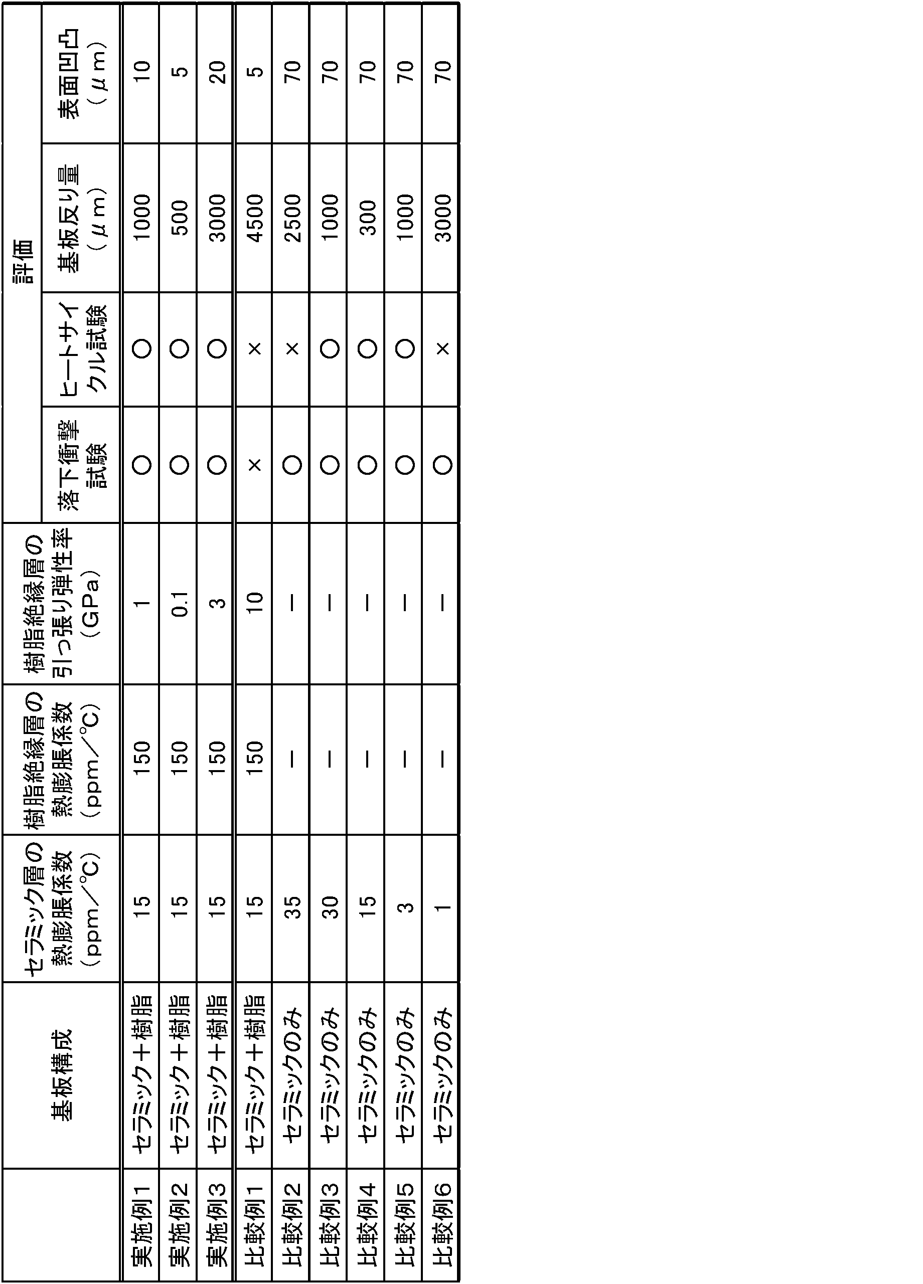
実施例1~3の複合基板では、セラミック層の表面に樹脂絶縁層が配置されており樹脂絶縁層の引っ張り弾性率が低いため表面凹凸が少なく、温度変化や落下衝撃に対して強い基板となっていた。
また、実施例1及び2の複合基板では特に引っ張り弾性率の低い樹脂絶縁層としているため、基板反り量及び表面凹凸がより低くなっていた。
比較例1の複合基板は樹脂絶縁層の引っ張り弾性率が高いため、温度変化や落下衝撃に対して弱い基板となっていた。
比較例2~6のセラミック基板はセラミック層の表面に樹脂絶縁層が配置されていないためセラミック層の表面に生じる凹凸がそのまま残っており、平滑性に劣っていた。
また、実施例1及び2の複合基板では特に引っ張り弾性率の低い樹脂絶縁層としているため、基板反り量及び表面凹凸がより低くなっていた。
比較例1の複合基板は樹脂絶縁層の引っ張り弾性率が高いため、温度変化や落下衝撃に対して弱い基板となっていた。
比較例2~6のセラミック基板はセラミック層の表面に樹脂絶縁層が配置されていないためセラミック層の表面に生じる凹凸がそのまま残っており、平滑性に劣っていた。
(実施例4)
樹脂フィルムとして引っ張り弾性率が0.1GPaであるフッ素樹脂系フィルムを使って作製した実施例2の複合基板の、樹脂絶縁層が配置されていない側の表面(セラミック基板の第2の表面)に対し、実施例1の記載で説明した方法と同様にして、実施例2で使用したフッ素樹脂系フィルムを高温圧着により接合した。その後、セラミック基板上の電極部分の樹脂フィルムに孔開け、金属導体ペーストを充填してからCu箔を300℃で高温圧着した。さらにCu箔エッチングにより配線パターンを形成し、それを繰り返すことで2層からなる第2の樹脂絶縁層を形成した。上記方法により複合基板を作製した。
樹脂フィルムとして引っ張り弾性率が0.1GPaであるフッ素樹脂系フィルムを使って作製した実施例2の複合基板の、樹脂絶縁層が配置されていない側の表面(セラミック基板の第2の表面)に対し、実施例1の記載で説明した方法と同様にして、実施例2で使用したフッ素樹脂系フィルムを高温圧着により接合した。その後、セラミック基板上の電極部分の樹脂フィルムに孔開け、金属導体ペーストを充填してからCu箔を300℃で高温圧着した。さらにCu箔エッチングにより配線パターンを形成し、それを繰り返すことで2層からなる第2の樹脂絶縁層を形成した。上記方法により複合基板を作製した。
(実施例5)
樹脂フィルムとして引っ張り弾性率が0.1GPaであり、熱膨張係数が30℃~400℃の範囲で250ppm/℃であるフッ素樹脂系フィルムを準備した。
このフッ素樹脂系フィルムを使用して実施例1と同様にしてセラミック基板の表面(セラミック基板の第1の表面)に樹脂絶縁層が配置された複合基板を作製した。さらに、この複合基板の、樹脂絶縁層が配置されていない側の表面(セラミック基板の第2の表面)に対し、このフッ素樹脂系フィルムを使用して実施例4と同様にして2層からなる第2の樹脂絶縁層を形成して複合基板を作製した。
樹脂フィルムとして引っ張り弾性率が0.1GPaであり、熱膨張係数が30℃~400℃の範囲で250ppm/℃であるフッ素樹脂系フィルムを準備した。
このフッ素樹脂系フィルムを使用して実施例1と同様にしてセラミック基板の表面(セラミック基板の第1の表面)に樹脂絶縁層が配置された複合基板を作製した。さらに、この複合基板の、樹脂絶縁層が配置されていない側の表面(セラミック基板の第2の表面)に対し、このフッ素樹脂系フィルムを使用して実施例4と同様にして2層からなる第2の樹脂絶縁層を形成して複合基板を作製した。
実施例4、5で作製した複合基板に対して、実施例1~3と同様にして、落下衝撃試験、ヒートサイクル試験、基板反り量の測定及び表面凹凸の測定を行った。それらの結果をまとめて表2に示した。

実施例4及び5に示す結果から、セラミック層の両面に樹脂絶縁層を配置することによって、基板の反り量をさらに低減させることができた。その他の特性評価項目も良好であった。
1、2、3、4 複合基板
10、10a、10b、10c、10d、10e セラミック層
11 層間接続用の金属導体
12 金属配線
20、20a、20b 樹脂絶縁層
21 層間接続用の金属導体
22 金属配線
30 第2の樹脂絶縁層
31 層間接続用の金属導体
32 金属配線
40 Cuポスト
42、43 はんだ
51、52、53 電子部品
10、10a、10b、10c、10d、10e セラミック層
11 層間接続用の金属導体
12 金属配線
20、20a、20b 樹脂絶縁層
21 層間接続用の金属導体
22 金属配線
30 第2の樹脂絶縁層
31 層間接続用の金属導体
32 金属配線
40 Cuポスト
42、43 はんだ
51、52、53 電子部品
Claims (9)
- セラミック層と、前記セラミック層の表面に配置された樹脂絶縁層とを有する複合基板であって、
前記セラミック層の熱膨張係数は30℃~400℃の範囲で3ppm/℃以上、30ppm/℃以下であり、前記樹脂絶縁層の引っ張り弾性率が3GPa以下であることを特徴とする複合基板。 - 前記樹脂絶縁層が前記セラミック層の表面に直接形成されている請求項1に記載の複合基板。
- 前記樹脂絶縁層の比誘電率εrが1.5以上3以下である請求項1又は2に記載の複合基板。
- 前記セラミック層及び前記樹脂絶縁層にはそれぞれ層間接続用の金属導体が設けられており、
前記セラミック層における金属導体を構成する金属材料はCuであり、
前記樹脂絶縁層における金属導体を構成する金属材料は、Sn、Mn及びNiの単体並びにCuとSn、Mn又はNiとの合金材料からなる群から選択された少なくとも1種の金属と、Cuとを含む材料からなる請求項1~3のいずれかに記載の複合基板。 - 前記樹脂絶縁層における層間接続用の金属導体は、Cu又はCuを含む合金からなる金属バルクであり、その上面側及び下面側の少なくとも一方がはんだ接合されている請求項1~4のいずれかに記載の複合基板。
- 前記セラミック層の表面のうち前記樹脂絶縁層が配置された第1の表面とは反対側に位置する第2の表面に、引っ張り弾性率が3GPa以下である第2の樹脂絶縁層が配置されている請求項1~5のいずれかに記載の複合基板。
- 熱膨張係数が30℃~400℃の範囲で3ppm/℃以上、30ppm/℃以下であるセラミック層からなるセラミック基板の表面に、引っ張り弾性率が3GPa以下である樹脂絶縁層となる樹脂フィルムを直接貼り付ける工程を行うことを特徴とする複合基板の製造方法。
- 前記セラミック基板の表面に前記樹脂フィルムを直接貼り付ける工程の後に、前記樹脂フィルムへの孔開け及び孔に対する層間接続用の金属導体の形成を行う請求項7に記載の複合基板の製造方法。
- 前記樹脂フィルムへの孔開け及び孔に対する層間接続用の金属導体の形成を行った後に、前記セラミック基板の表面に前記樹脂フィルムを直接貼り付ける工程を行う請求項7に記載の複合基板の製造方法。
Applications Claiming Priority (2)
| Application Number | Priority Date | Filing Date | Title |
|---|---|---|---|
| JP2016048806 | 2016-03-11 | ||
| JP2016-048806 | 2016-03-11 |
Publications (1)
| Publication Number | Publication Date |
|---|---|
| WO2017154570A1 true WO2017154570A1 (ja) | 2017-09-14 |
Family
ID=59789394
Family Applications (1)
| Application Number | Title | Priority Date | Filing Date |
|---|---|---|---|
| PCT/JP2017/006501 Ceased WO2017154570A1 (ja) | 2016-03-11 | 2017-02-22 | 複合基板及び複合基板の製造方法 |
Country Status (1)
| Country | Link |
|---|---|
| WO (1) | WO2017154570A1 (ja) |
Cited By (1)
| Publication number | Priority date | Publication date | Assignee | Title |
|---|---|---|---|---|
| US11284508B2 (en) | 2019-08-06 | 2022-03-22 | At&S Austria Technologie & Systemtechnik Aktiengesellschaft | Semi-flex component carrier with dielectric material having high elongation and low young modulus |
Citations (3)
| Publication number | Priority date | Publication date | Assignee | Title |
|---|---|---|---|---|
| JPH0621649A (ja) * | 1992-04-03 | 1994-01-28 | Internatl Business Mach Corp <Ibm> | 多層超小型電子回路モジュール及びその形成方法 |
| JP2004327803A (ja) * | 2003-04-25 | 2004-11-18 | Hitachi Chem Co Ltd | 多層回路基板、半導体チップ搭載基板及び半導体パッケージ、並びにそれらの製造方法 |
| JP2016032098A (ja) * | 2014-07-25 | 2016-03-07 | Jsr株式会社 | 回路基板用樹脂基板、回路基板用樹脂組成物および回路基板 |
-
2017
- 2017-02-22 WO PCT/JP2017/006501 patent/WO2017154570A1/ja not_active Ceased
Patent Citations (3)
| Publication number | Priority date | Publication date | Assignee | Title |
|---|---|---|---|---|
| JPH0621649A (ja) * | 1992-04-03 | 1994-01-28 | Internatl Business Mach Corp <Ibm> | 多層超小型電子回路モジュール及びその形成方法 |
| JP2004327803A (ja) * | 2003-04-25 | 2004-11-18 | Hitachi Chem Co Ltd | 多層回路基板、半導体チップ搭載基板及び半導体パッケージ、並びにそれらの製造方法 |
| JP2016032098A (ja) * | 2014-07-25 | 2016-03-07 | Jsr株式会社 | 回路基板用樹脂基板、回路基板用樹脂組成物および回路基板 |
Cited By (2)
| Publication number | Priority date | Publication date | Assignee | Title |
|---|---|---|---|---|
| US11284508B2 (en) | 2019-08-06 | 2022-03-22 | At&S Austria Technologie & Systemtechnik Aktiengesellschaft | Semi-flex component carrier with dielectric material having high elongation and low young modulus |
| US12058810B2 (en) | 2019-08-06 | 2024-08-06 | AT&SAustria Technologie &Systemtechnik AG | Semi-flex component carrier with dielectric material having high elongation and low young modulus |
Similar Documents
| Publication | Publication Date | Title |
|---|---|---|
| JP4401070B2 (ja) | 半導体装置内蔵多層配線基板及びその製造方法 | |
| US7580240B2 (en) | Via array capacitor, wiring board incorporating a via array capacitor, and method of manufacturing the same | |
| US20040173891A1 (en) | Intermediate board, intermediate board with a semiconductor device, substrate board with an intermediate board, structural member including a semiconductor device, an intermediate board and a substrate board, and method of producing an intermediate board | |
| US20070178279A1 (en) | Hybrid multilayer substrate and method for manufacturing the same | |
| US8421215B2 (en) | Laminated and sintered ceramic circuit board, and semiconductor package including the circuit board | |
| KR20180017117A (ko) | 배선 회로 기판, 반도체 장치, 배선 회로 기판의 제조 방법 및 반도체 장치의 제조 방법 | |
| US20200203266A1 (en) | Substrate, method of manufacturing substrate, and electronic device | |
| US6335076B1 (en) | Multi-layer wiring board and method for manufacturing the same | |
| US20140224532A1 (en) | Thin-film wiring substrate and substrate for probe card | |
| KR20070049133A (ko) | 적층 기판, 그 제조 방법 및 그 적층 기판을 갖는 전자기기 | |
| US7226654B2 (en) | Laminated wiring board and its mounting structure | |
| JP2004274035A (ja) | 電子部品内蔵モジュールとその製造方法 | |
| JPH01236698A (ja) | コンデンサ内蔵セラミック多層回路基板 | |
| WO2017154570A1 (ja) | 複合基板及び複合基板の製造方法 | |
| WO2020022109A1 (ja) | 複合基板及び複合基板の製造方法 | |
| TW202545719A (zh) | 多層基板 | |
| CN101783333B (zh) | 改善倒装芯片基板变形的结构 | |
| US9007777B2 (en) | Board module and fabrication method thereof | |
| JP2012167008A (ja) | ガラスセラミック組成物、ガラスセラミック焼結体並びにそれを用いた配線基板とその実装構造 | |
| JP2011151048A (ja) | 電子部品の製造方法および電子部品 | |
| JP2007173862A (ja) | 中継基板、半導体素子付き中継基板、中継基板付き基板、半導体素子と中継基板と基板とからなる構造体 | |
| KR20050114189A (ko) | 적층 기판, 그 제조 방법 및 그 적층 기판을 갖는 전자기기 | |
| JP2007221117A (ja) | 部品内蔵基板およびその製造方法 | |
| JP5383962B2 (ja) | ガラスセラミック組成物、ガラスセラミック焼結体並びにそれを用いた配線基板とその実装構造 | |
| JP2019140216A (ja) | 回路基板及び回路基板の製造方法 |
Legal Events
| Date | Code | Title | Description |
|---|---|---|---|
| NENP | Non-entry into the national phase |
Ref country code: DE |
|
| 121 | Ep: the epo has been informed by wipo that ep was designated in this application |
Ref document number: 17762912 Country of ref document: EP Kind code of ref document: A1 |
|
| 122 | Ep: pct application non-entry in european phase |
Ref document number: 17762912 Country of ref document: EP Kind code of ref document: A1 |
|
| NENP | Non-entry into the national phase |
Ref country code: JP |