WO2017149608A1 - 撮像装置及び撮像方法 - Google Patents
撮像装置及び撮像方法 Download PDFInfo
- Publication number
- WO2017149608A1 WO2017149608A1 PCT/JP2016/056095 JP2016056095W WO2017149608A1 WO 2017149608 A1 WO2017149608 A1 WO 2017149608A1 JP 2016056095 W JP2016056095 W JP 2016056095W WO 2017149608 A1 WO2017149608 A1 WO 2017149608A1
- Authority
- WO
- WIPO (PCT)
- Prior art keywords
- image
- pixel
- imaging
- light
- luminance
- Prior art date
- Legal status (The legal status is an assumption and is not a legal conclusion. Google has not performed a legal analysis and makes no representation as to the accuracy of the status listed.)
- Ceased
Links
Images








Classifications
-
- G—PHYSICS
- G01—MEASURING; TESTING
- G01J—MEASUREMENT OF INTENSITY, VELOCITY, SPECTRAL CONTENT, POLARISATION, PHASE OR PULSE CHARACTERISTICS OF INFRARED, VISIBLE OR ULTRAVIOLET LIGHT; COLORIMETRY; RADIATION PYROMETRY
- G01J4/00—Measuring polarisation of light
- G01J4/04—Polarimeters using electric detection means
-
- G—PHYSICS
- G06—COMPUTING OR CALCULATING; COUNTING
- G06T—IMAGE DATA PROCESSING OR GENERATION, IN GENERAL
- G06T1/00—General purpose image data processing
- G06T1/0007—Image acquisition
-
- G—PHYSICS
- G01—MEASURING; TESTING
- G01J—MEASUREMENT OF INTENSITY, VELOCITY, SPECTRAL CONTENT, POLARISATION, PHASE OR PULSE CHARACTERISTICS OF INFRARED, VISIBLE OR ULTRAVIOLET LIGHT; COLORIMETRY; RADIATION PYROMETRY
- G01J3/00—Spectrometry; Spectrophotometry; Monochromators; Measuring colours
- G01J3/02—Details
- G01J3/0205—Optical elements not provided otherwise, e.g. optical manifolds, diffusers, windows
- G01J3/0224—Optical elements not provided otherwise, e.g. optical manifolds, diffusers, windows using polarising or depolarising elements
-
- G—PHYSICS
- G01—MEASURING; TESTING
- G01J—MEASUREMENT OF INTENSITY, VELOCITY, SPECTRAL CONTENT, POLARISATION, PHASE OR PULSE CHARACTERISTICS OF INFRARED, VISIBLE OR ULTRAVIOLET LIGHT; COLORIMETRY; RADIATION PYROMETRY
- G01J3/00—Spectrometry; Spectrophotometry; Monochromators; Measuring colours
- G01J3/28—Investigating the spectrum
- G01J3/2803—Investigating the spectrum using photoelectric array detector
-
- G—PHYSICS
- G01—MEASURING; TESTING
- G01J—MEASUREMENT OF INTENSITY, VELOCITY, SPECTRAL CONTENT, POLARISATION, PHASE OR PULSE CHARACTERISTICS OF INFRARED, VISIBLE OR ULTRAVIOLET LIGHT; COLORIMETRY; RADIATION PYROMETRY
- G01J3/00—Spectrometry; Spectrophotometry; Monochromators; Measuring colours
- G01J3/28—Investigating the spectrum
- G01J3/2823—Imaging spectrometer
-
- G—PHYSICS
- G01—MEASURING; TESTING
- G01J—MEASUREMENT OF INTENSITY, VELOCITY, SPECTRAL CONTENT, POLARISATION, PHASE OR PULSE CHARACTERISTICS OF INFRARED, VISIBLE OR ULTRAVIOLET LIGHT; COLORIMETRY; RADIATION PYROMETRY
- G01J3/00—Spectrometry; Spectrophotometry; Monochromators; Measuring colours
- G01J3/46—Measurement of colour; Colour measuring devices, e.g. colorimeters
- G01J3/50—Measurement of colour; Colour measuring devices, e.g. colorimeters using electric radiation detectors
- G01J3/51—Measurement of colour; Colour measuring devices, e.g. colorimeters using electric radiation detectors using colour filters
- G01J3/513—Measurement of colour; Colour measuring devices, e.g. colorimeters using electric radiation detectors using colour filters having fixed filter-detector pairs
-
- G—PHYSICS
- G02—OPTICS
- G02B—OPTICAL ELEMENTS, SYSTEMS OR APPARATUS
- G02B5/00—Optical elements other than lenses
- G02B5/20—Filters
- G02B5/201—Filters in the form of arrays
-
- G—PHYSICS
- G02—OPTICS
- G02B—OPTICAL ELEMENTS, SYSTEMS OR APPARATUS
- G02B5/00—Optical elements other than lenses
- G02B5/30—Polarising elements
- G02B5/3025—Polarisers, i.e. arrangements capable of producing a definite output polarisation state from an unpolarised input state
-
- G—PHYSICS
- G02—OPTICS
- G02B—OPTICAL ELEMENTS, SYSTEMS OR APPARATUS
- G02B5/00—Optical elements other than lenses
- G02B5/30—Polarising elements
- G02B5/3025—Polarisers, i.e. arrangements capable of producing a definite output polarisation state from an unpolarised input state
- G02B5/3058—Polarisers, i.e. arrangements capable of producing a definite output polarisation state from an unpolarised input state comprising electrically conductive elements, e.g. wire grids, conductive particles
-
- G—PHYSICS
- G06—COMPUTING OR CALCULATING; COUNTING
- G06F—ELECTRIC DIGITAL DATA PROCESSING
- G06F21/00—Security arrangements for protecting computers, components thereof, programs or data against unauthorised activity
- G06F21/30—Authentication, i.e. establishing the identity or authorisation of security principals
- G06F21/31—User authentication
- G06F21/32—User authentication using biometric data, e.g. fingerprints, iris scans or voiceprints
-
- H—ELECTRICITY
- H04—ELECTRIC COMMUNICATION TECHNIQUE
- H04N—PICTORIAL COMMUNICATION, e.g. TELEVISION
- H04N23/00—Cameras or camera modules comprising electronic image sensors; Control thereof
- H04N23/10—Cameras or camera modules comprising electronic image sensors; Control thereof for generating image signals from different wavelengths
-
- H—ELECTRICITY
- H04—ELECTRIC COMMUNICATION TECHNIQUE
- H04N—PICTORIAL COMMUNICATION, e.g. TELEVISION
- H04N23/00—Cameras or camera modules comprising electronic image sensors; Control thereof
- H04N23/50—Constructional details
- H04N23/55—Optical parts specially adapted for electronic image sensors; Mounting thereof
-
- H—ELECTRICITY
- H04—ELECTRIC COMMUNICATION TECHNIQUE
- H04N—PICTORIAL COMMUNICATION, e.g. TELEVISION
- H04N23/00—Cameras or camera modules comprising electronic image sensors; Control thereof
- H04N23/56—Cameras or camera modules comprising electronic image sensors; Control thereof provided with illuminating means
-
- H—ELECTRICITY
- H04—ELECTRIC COMMUNICATION TECHNIQUE
- H04N—PICTORIAL COMMUNICATION, e.g. TELEVISION
- H04N23/00—Cameras or camera modules comprising electronic image sensors; Control thereof
- H04N23/60—Control of cameras or camera modules
-
- H—ELECTRICITY
- H04—ELECTRIC COMMUNICATION TECHNIQUE
- H04N—PICTORIAL COMMUNICATION, e.g. TELEVISION
- H04N23/00—Cameras or camera modules comprising electronic image sensors; Control thereof
- H04N23/70—Circuitry for compensating brightness variation in the scene
- H04N23/71—Circuitry for evaluating the brightness variation
-
- H—ELECTRICITY
- H04—ELECTRIC COMMUNICATION TECHNIQUE
- H04N—PICTORIAL COMMUNICATION, e.g. TELEVISION
- H04N23/00—Cameras or camera modules comprising electronic image sensors; Control thereof
- H04N23/70—Circuitry for compensating brightness variation in the scene
- H04N23/74—Circuitry for compensating brightness variation in the scene by influencing the scene brightness using illuminating means
-
- H—ELECTRICITY
- H04—ELECTRIC COMMUNICATION TECHNIQUE
- H04N—PICTORIAL COMMUNICATION, e.g. TELEVISION
- H04N23/00—Cameras or camera modules comprising electronic image sensors; Control thereof
- H04N23/70—Circuitry for compensating brightness variation in the scene
- H04N23/75—Circuitry for compensating brightness variation in the scene by influencing optical camera components
-
- H—ELECTRICITY
- H04—ELECTRIC COMMUNICATION TECHNIQUE
- H04N—PICTORIAL COMMUNICATION, e.g. TELEVISION
- H04N25/00—Circuitry of solid-state image sensors [SSIS]; Control thereof
- H04N25/70—SSIS architectures; Circuits associated therewith
-
- G—PHYSICS
- G01—MEASURING; TESTING
- G01J—MEASUREMENT OF INTENSITY, VELOCITY, SPECTRAL CONTENT, POLARISATION, PHASE OR PULSE CHARACTERISTICS OF INFRARED, VISIBLE OR ULTRAVIOLET LIGHT; COLORIMETRY; RADIATION PYROMETRY
- G01J3/00—Spectrometry; Spectrophotometry; Monochromators; Measuring colours
- G01J3/28—Investigating the spectrum
- G01J3/2823—Imaging spectrometer
- G01J2003/2826—Multispectral imaging, e.g. filter imaging
Definitions
- the present invention relates to an imaging apparatus and an imaging method.
- Biometric authentication is used for authentication of whether or not an operator of a computer or the like is a valid operator, for example, authentication of an operator of a deposit / withdrawal device in a store.
- the imaging device images, for example, a vein of a person's palm.
- An individual is authenticated when a vein pattern based on an image captured by the imaging device matches a vein pattern registered in advance.
- the deposit / withdrawal apparatus accepts an operation only by an operator who is biometrically authenticated.
- the imaging device for each application including biometric authentication irradiates infrared light to the palm held in the imaging direction of the imaging device.
- a part of the infrared light is reflected by the surface of the palm, but a part of the infrared light passes through the epidermis and is absorbed by the hemoglobin in the vein inside the hand.
- the vein pattern inside a palm can be acquired by imaging with an image sensor with infrared light sensitivity.
- such an imaging apparatus has a self-illuminating device that irradiates infrared light, irradiates the palm with uniform light through a ring-shaped light guide, and acquires a palm image with an imaging system including a lens and an image sensor.
- the acquired palm image also includes a background such as a ceiling or a wall, and depending on the conditions, there is a case where palm extraction or vein pattern signal extraction is adversely affected in the image processing stage.
- a method is used in which the self-illuminating device is imaged under two conditions of turning on and off, and the difference image is used as a palm image.
- the same background exists in each image when the self-illuminating device is turned on and off, and the background is canceled in the difference image, and an image of only the palm is obtained.
- ambient light such as sunlight and room light not only illuminates the background, but also illuminates the palm together with the self-illuminator.
- illumination of the palm by such ambient light and external light may also have an adverse effect on the signal extraction of the vein pattern, it is canceled by the differential image, and an image illuminated only on the self-illuminating device is obtained (for example, patent document) 1).
- the disclosed technique has been made in view of the above, and an object of the present invention is to provide an imaging apparatus and an imaging method capable of extracting a vein pattern with high accuracy, for example.
- the imaging apparatus includes an image sensor, a pixel selection unit, and an image output unit.
- the image sensor images the imaging target through a polarizing plate provided so that the polarization direction is different for each pixel of a pixel group including a plurality of pixels corresponding to each point of the imaging target.
- the pixel selection unit selects a pixel having the minimum luminance for each pixel group corresponding to each point.
- the image output unit outputs a captured image of the imaging target generated from the pixel selected by the pixel selection unit.
- a vein pattern can be extracted with high accuracy.
- FIG. 1 is a block diagram illustrating an example of an imaging apparatus according to the first embodiment.
- FIG. 2A is a perspective view illustrating an example of an imaging apparatus according to the first embodiment.
- FIG. 2B is a cross-sectional view taken along the line II illustrating an example of the imaging device according to the first embodiment.
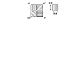
- FIG. 3A is a diagram illustrating an example of a configuration of a color image sensor.
- FIG. 3B is a diagram illustrating an example of the configuration of the multi-polarization image sensor in the imaging apparatus according to the first embodiment.
- FIG. 4 is a diagram illustrating an example of a pixel configuration method of the color image sensor.
- FIG. 1 is a block diagram illustrating an example of an imaging apparatus according to the first embodiment.
- FIG. 2A is a perspective view illustrating an example of an imaging apparatus according to the first embodiment.
- FIG. 2B is a cross-sectional view taken along the line II illustrating an example of the imaging device according to the first embodiment.
- FIG. 3A
- FIG. 5A is a diagram illustrating an example of a pixel configuration method of the multi-polarization image sensor of the imaging apparatus according to the first embodiment.
- FIG. 5B is a diagram illustrating an example of a pixel configuration method of the multi-polarization image sensor of the imaging apparatus according to the first embodiment.
- FIG. 6A is a diagram illustrating an example of the behavior of reflected light from the imaging target in the imaging apparatus according to the first embodiment.
- FIG. 6B is a diagram illustrating an example of the behavior of reflected light from the imaging target in the imaging apparatus according to the first embodiment.
- FIG. 7 is a perspective view showing specular reflection and change in polarization direction on the object surface.
- FIG. 8 is a diagram schematically showing the relationship between regular reflection and the polarization direction from the normal direction of the object surface.
- FIG. 9 is a diagram showing the palm when illuminated with strong external light.
- FIG. 10 is a diagram illustrating an example of a luminance distribution of an image including regular reflection among reflected light from an imaging target in the imaging apparatus according to the first embodiment.
- FIG. 11A is a diagram illustrating an example of a luminance distribution of an image when the self-illumination device is turned on under strong external light in the imaging apparatus according to the first embodiment.
- FIG. 11B is a diagram illustrating an example of an image luminance distribution when the self-illuminating device is off under strong external light in the imaging apparatus according to the first embodiment.
- FIG. 10 is a diagram illustrating an example of a luminance distribution of an image including regular reflection among reflected light from an imaging target in the imaging apparatus according to the first embodiment.
- FIG. 11A is a diagram illustrating an example of a luminance distribution of an image when the self-illumination device is turned on under strong external light in the imaging apparatus according to the first embodiment.
- FIG. 11B is a diagram
- FIG. 11C is a diagram illustrating an example of a luminance distribution of a difference image when the self-illuminating device is turned on and off under strong external light in the imaging apparatus according to the first embodiment.
- FIG. 12 is a flowchart illustrating an example of an imaging process in the imaging apparatus according to the first embodiment.
- FIG. 13 is a diagram illustrating another example of a configuration method of a color image sensor.
- an imaging apparatus applied to a vein authentication apparatus that authenticates a person from the characteristics of a person's vein will be described as an example, but the disclosed technique is not limited.
- the disclosed technique is applicable to, for example, an imaging apparatus in general that acquires target biological information from a difference image.
- the embodiments can be appropriately combined within a consistent range.
- symbol is provided to the same structure and process, and description of an existing structure and process is abbreviate
- FIG. 1 is a block diagram illustrating an example of an imaging apparatus according to the first embodiment.
- FIG. 2A is a perspective view illustrating an example of an imaging apparatus according to the first embodiment.
- FIG. 2B is a cross-sectional view taken along the line II illustrating an example of the imaging device according to the first embodiment.
- the imaging apparatus 100 includes a control unit 110, an image sensor 120, and a light emitting element 130 which are processing devices such as a microcomputer.
- the imaging unit 1 is accommodated in a casing 100a, and is covered with a cover 100b that is transparent to infrared light.
- the imaging device 100 captures an image of the palm held up from above the cover 100b.
- the imaging unit 1 of the imaging apparatus 100 has an image sensor 120, a light emitting element 130, a lens unit 3, and a light guide 4 on a substrate 2.
- the control unit 110 is provided on the control board 5.
- the light emitted from the light emitting element 130 passes through the light guide 4 and is emitted upward from the cover 100b as illumination light. This light illuminates the palm held from above the cover 100b, and is reflected or absorbed by the palm.
- the image sensor 120 passes through the lens of the lens unit 3 and captures an image of the palm held up from above the cover 100b.
- the image sensor 120 is a multi-polarization image sensor that constitutes one pixel for every four image sensors each provided with a polarizing plate having a different polarization direction, for example.
- a pixel configuration method in the image sensor 120 will be described.
- the multi-polarization image sensor is configured based on the same concept as the color image sensor, and the color filter of the color image sensor is replaced with a polarizing plate.
- FIG. 3A is a diagram showing an example of the configuration of a color image sensor.
- color image sensors corresponding to the three primary colors R (Red), G (Green), and B (Blue) are arranged in a Bayer array.
- the arrangement pattern shown in FIG. 3A is repeated in the sensor area of the color image sensor.
- FIG. 3B is a diagram illustrating an example of the configuration of the multi-polarization image sensor in the imaging apparatus according to the first embodiment.
- a multi-polarization image sensor is configured based on the configuration method of the color image sensor shown in FIG. 3A.
- the pixel B in FIG. 3A is replaced with a pixel provided with a polarizing plate whose lattice direction is 0 °.
- the G pixel on the upper right side shown in FIG. 3A is replaced with a pixel provided with a polarizing plate whose lattice direction is 45 °.
- the R pixel in FIG. 3A is replaced with a pixel provided with a polarizing plate whose lattice direction is 90 °.
- the G pixel on the lower left side shown in FIG. 3A is replaced with a pixel provided with a polarizing plate having a lattice direction of 135 °.
- a wire grid type polarizing plate is assumed, and the transmission direction and the reflection direction of polarized light of each polarizing plate are transmitted when the direction of polarized light is orthogonal to the direction of the grating as shown in FIG. 3B. If the direction of polarization and the direction of the grating coincide, the light is reflected. Since the direction of polarization to be transmitted or reflected is determined by the direction of the grating, the term “polarization direction of the polarizing plate” is used in this specification instead of the term “direction of the grating”. In principle, it is also possible to use an absorption-type polarizing plate, in which case the above-described reflection is replaced by absorption.
- polarizing plates having different polarization directions are provided for each of the four pixels, and a multi-polarization image sensor is configured by repeating this arrangement over the entire sensor area in the same manner as a color image sensor.
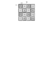
- FIG. 4 is a diagram illustrating an example of a pixel configuration method of the color image sensor.
- one pixel is represented by four pixels having different properties.
- the upper left broken line encircled portion 11 includes one R and one B and two Gs, but it is assumed that this constitutes one pixel.
- the output of G is the average value of the two G outputs.
- a broken line encircled portion 12 shifted to the right by one column is considered as one right pixel.
- the broken line encircled part 12 shares one G and B, but uses another G and R. In this way, the horizontal pixels in FIG. 4 are configured.
- the pixels in the vertical direction in FIG. 4 are configured.
- the multi-polarization image sensor also constitutes pixels in the same way as the color image sensor.
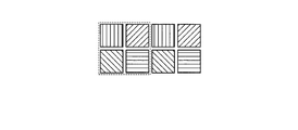
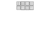
- 5A and 5B are diagrams illustrating an example of a pixel configuration method of the multi-polarization image sensor of the imaging apparatus according to the first embodiment. As indicated by the broken line in FIG. 5A, one pixel is composed of four polarization directions of 0 °, 45 °, 90 °, and 135 °. One pixel to the right is formed by a broken line box shifted to the right by one column as shown in FIG. 5B. By shifting the pixel configuration one by one in the horizontal direction and the vertical direction, an image having polarization characteristics in four directions can be acquired while maintaining the number of output pixels as in the color image sensor.
- 6A and 6B are diagrams illustrating an example of behavior of reflected light from an imaging target in the imaging apparatus according to the first embodiment.
- the dynamic range of the brightness is expanded by the local high-brightness area, and the signal level is lowered as a whole, or the minute signal disappears by hiding in the local high-brightness area.
- the generation of the local high-luminance region is mainly caused by the illumination light being specularly reflected on the palm surface and riding on the image.
- the external light illumination is randomly polarized, the component of the light that is regularly reflected on the object surface has a bias that the S-polarized component becomes stronger.
- the light incident on the object is not only reflected on the surface of the object, but also reflected in the form of penetrating the inside of the object, scattering and reflecting, and coming out of the surface.
- the light penetrating inside is repeatedly scattered and reflected in the human skin tissue and emitted from the surface, but has little directivity and isotropically diffuses.
- light is diffusely reflected in various directions even with minute irregularities on the surface of the object.
- diffuse reflection since the reflection is repeated, the polarization direction is disturbed, and even if the incident light is linearly polarized light, the diffusely reflected light becomes random.
- some light is specularly reflected (specularly reflected) on the surface of the object. Unlike diffuse reflection, regular reflection has a strong directivity in the direction of specular reflection.
- Specular reflection light is also characterized by polarization characteristics.
- the reflectance of light on the object surface differs depending on the polarization direction, and the P-polarized light whose electric field is oscillating in the incident surface is easy to transmit through the interface and has a low reflectance.
- the S-polarized light whose electric field vibration is perpendicular to the incident surface that is, parallel to the interface, has a high reflectance. Therefore, even if the incident light is randomly polarized light, the specularly reflected light is light having a strong S-polarized component.
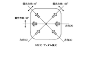
- FIG. 7 is a perspective view showing this phenomenon, that is, the regular reflection on the object surface and the change in the polarization direction.
- FIG. 8 is a diagram schematically showing the relationship between specular reflection and the polarization direction in a plan view viewed from the normal direction of the object surface.
- the polarization direction of light regularly reflected on the object surface is mainly S-polarized light, that is, the direction perpendicular to the incident surface. Therefore, when randomly polarized illumination light enters from the direction of FIG. 8A, the polarization direction of the light that is regularly reflected on the object surface is mainly 90 °.
- the regular reflection of illumination light incident from the direction (B) is mainly 45 °
- the regular reflection of illumination light incident from the direction (C) is mainly 135 °.
- Example 1 realizes a function of eliminating the specularly reflected light to a practically sufficient level by utilizing the fact that four adjacent pixels of a multi-polarized image sensor transmit polarized light in different directions. As a result, even when using external light illumination that is randomly polarized and cannot control the incident direction, it is possible to expect an effect that a good palm image without a local high-brightness region can be acquired.
- FIG. 9 shows a palm when illuminated with strong external light such as sunlight.
- the light imaged on the sensor surface of the image sensor 120 by the lens unit 3 is shown. That is, the palm image in FIG. 9 is an input signal to the image sensor 120, and this light undergoes intensity modulation by the polarizing plate of the multi-polarization image sensor and is converted into a pixel signal of the image sensor 120.
- the polarizing plate in the direction of 135 ° transmits a large amount of regular reflection light, and the luminance of the pixel increases.
- the directions of 0 ° and 90 ° are large, and the luminance of the pixel in the 45 ° direction with the least amount of transmitted light that reflects the specularly reflected light from the lower right most strongly is the smallest.
- the external light illumination that forms the local high-brightness region at the lower right is incident from the direction (A) in FIG.
- the 90 ° direction among the four different polarization directions of the multi-polarization image sensor The polarizing plate reflects the specularly reflected light most strongly and does not transmit it. That is, it is considered that the intensity of the light transmitted through the polarizing plate in the 90 ° direction is the smallest and is almost diffusely reflected light.
- the light emitting element 130 is a light source such as an LED (Light Emitting Diode) that irradiates the palm of the imaging target held over the imaging apparatus 100 with randomly polarized light.
- the light emitting element 130 may be referred to as self-illumination.
- ambient light such as sunlight or room light
- external light illumination ambient light
- the self-illumination light and the external light illumination light may be collectively referred to as illumination light.
- the control unit 110 includes a lighting control unit 110a, an image acquisition unit 110b, a pixel selection unit 110c, and an image output unit 110d.
- the lighting control unit 110 a controls lighting and extinguishing of the light emitting element 130.
- the image acquisition unit 110b instructs the lighting control unit 110a to turn off the light emitting element 130. Then, the image acquisition unit 110b captures an image including the palm and the background held by the imaging device 100 (hereinafter, may be referred to as an external light image) on the image sensor 130 with the light emitting element 130 turned off. To get it. Outside light is light other than self-illumination, such as outdoor natural light or indoor indoor illumination light.
- the image acquisition unit 110b instructs the lighting control unit 110a to turn on the light emitting element 130. Then, the image acquisition unit 110b captures an image including the palm and the background held over the imaging device 100 (hereinafter, may be referred to as a self-illuminated image) on the image sensor 130 in a state where the light emitting element 130 is turned on. To get it.
- the image acquisition unit 110b acquires a difference image between the external light image and the self-illuminated image.
- the image acquisition unit 110b is configured such that the luminance of a predetermined portion of the external light image (for example, the central portion of the image) is equal to or higher than the first threshold value, or the predetermined portion of the differential image between the external light image and the self-illuminated image It is determined whether or not the luminance is less than the second threshold value.
- the image acquisition unit 110b Is a pixel selection processing target image.
- the difference image is set as a pixel selection processing target image.
- the image acquisition unit 110b has a case where the luminance of the predetermined portion of the difference image between the external light image and the self-illuminated image is less than the second threshold even if the luminance of the predetermined portion of the external light image is less than the first threshold.
- the outside light image is set as a pixel selection processing target image.
- the pixel selection unit 110c selects a pixel having the minimum luminance for each pixel group in which four adjacent pixels are grouped, among the pixels of the processing target image. Adjacent four pixels refer to four pixels arranged in a grid.
- the image output unit 110d connects the pixels selected by the pixel selection unit 110c to generate one palm image.
- FIG. 10 is a diagram illustrating an example of a luminance distribution of an image including regular reflection among reflected light from an imaging target in the imaging apparatus according to the first embodiment.
- the lower right regular reflection region in the upper palm diagram of FIG. 10 has locally high luminance in the luminance distribution graph shown in the lower portion of FIG.
- the luminance distribution of the entire palm image is obtained by superimposing local high luminance due to specularly reflected light incident on the lens on a signal image created by diffusely reflected light. Therefore, if regular reflection is eliminated, a continuous image by diffuse reflected light can be acquired.
- the minimum value among the luminance outputs in the four polarization directions it is possible to greatly reduce the specularly reflected light due to the randomly polarized illumination, reducing the inconvenience of the uneven distribution of the luminance distribution in one image, Sufficient continuity of pixels in image data can be expected.
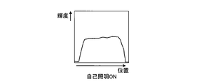
- FIG. 11A is a diagram illustrating an example of a luminance distribution of an image when the self-illumination device is turned on under strong external light in the imaging apparatus according to the first embodiment.
- FIG. 11B is a diagram illustrating an example of an image luminance distribution when the self-illuminating device is off under strong external light in the imaging apparatus according to the first embodiment.
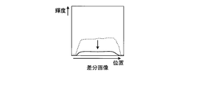
- FIG. 11C is a diagram illustrating an example of a luminance distribution of a difference image when the self-illuminating device is turned on and off under strong external light in the imaging apparatus according to the first embodiment.
- the difference image between the external light image and the self-illuminated image is also illustrated in FIG. As shown by the broken line in FIG. 4, the image has a sufficient difference in luminance.
- the difference image between the external light image and the self-illuminated image increases the brightness of the self-illuminated image as shown by the solid line in FIG. 11B, and the solid line illustrated in FIG. 11C.
- the image does not have a sufficient difference in luminance.
- both the self-illumination ON shown in FIG. 11A and the self-illumination OFF shown in FIG. 11B increase in luminance, so exposure is performed so that the luminance is not saturated. Time will be shortened. Therefore, the brightness difference of the difference image between the external light image and the self-illuminated image is reduced. As described above, when the luminance difference is reduced, the influence of light and circuit noise is increased, which adversely affects the image processing of palm vein pattern extraction.
- the method for acquiring the palm vein pattern based on the difference image is switched to the method for acquiring the palm vein pattern based only on the external light image based on the threshold determination.
- the palm vein pattern based only on the external light image is obtained from the palm vein pattern acquisition method based on the difference image.
- luminance of the difference image shown to FIG. 11C becomes less than 2nd threshold value, it switches from the acquisition method of the palm vein pattern by a difference image to the acquisition method of the palm vein pattern only by an external light image.
- the palm is imaged by self-illumination in indoors where the intensity of external light is less than a predetermined intensity.
- the external light intensity increases due to use at the window or outdoors, the appropriate exposure time for acquiring the difference image between the self-illumination ON and OFF is shortened. For this reason, in the first embodiment, on the basis of a certain condition, the method is switched from the palm vein pattern acquisition method using the difference image to the palm vein pattern acquisition method using only the external light image.
- FIG. 12 is a flowchart illustrating an example of an imaging process in the imaging apparatus according to the first embodiment.
- the imaging apparatus 100 determines whether or not to image the palm (step S11).
- the imaging apparatus 100 moves the process to step S12.
- the imaging device 100 repeats step S11 when not imaging the palm (step S11: No).
- step S12 the imaging apparatus 100 turns off the self-illumination.
- the imaging apparatus 100 acquires an external light image of the palm (step S13).
- the imaging apparatus 100 determines whether or not the brightness of the external light image (for example, a predetermined portion thereof) is equal to or higher than the first threshold (step S14).
- the imaging apparatus 100 moves the process to step S21.
- the imaging apparatus 100 moves the process to step S15.
- step S15 the imaging apparatus 100 turns on self-illumination.
- the imaging device 100 acquires a self-illuminated image (step S16).
- the imaging apparatus 100 turns off the self-illumination (step S17).
- the imaging apparatus 100 acquires a difference image between the external light image acquired in step S13 and the self-illuminated image acquired in step S16 (step S18).
- the imaging apparatus 100 determines whether or not the luminance of the difference image (for example, a predetermined portion thereof) is less than the second threshold (step S19).
- the imaging apparatus 100 moves the process to step S21.
- the imaging apparatus 100 moves the process to step S20.
- step S20 the imaging apparatus 100 sets the difference image as a processing target image.
- step S21 the imaging apparatus 100 sets the external light image as a processing target image.
- step S22 the imaging apparatus 100 selects a pixel having the minimum luminance for each pixel group from the processing target image. Then, the imaging apparatus 100 generates an output image from the pixels selected in step S22 (step S23). Next, the imaging apparatus 100 determines whether or not to end the imaging process (step S24). When ending the imaging process (step S24: Yse), the imaging apparatus 100 ends the imaging process, and when not ending the imaging process (step S24: No), the process moves to step S11.
- step S19 when the luminance of the difference image (for example, a predetermined portion thereof) is less than the second threshold (step S19: Yes), the imaging apparatus 100 does not perform the processing of steps S21 to S24, but performs step The process may be moved to S11. Alternatively, only the first threshold determination in S14 may be performed, and the process in S19 may be deleted.
- step S22 to step S23 is immediately performed on the acquired image for pixel selection and output image generation. Image acquisition may not be performed.
- each of the “first image” and the “second image” may be an “external light image” and a “self-illumination image”, or a “self-illumination image” and an “external light image”. Either is acceptable.
- Example 1 it is possible to obtain a good palm image excluding a local high-brightness region such as shine while using external light as illumination.
- control unit 110 of the imaging device 100 performs various processes shown in the flowchart of FIG. 12, but the present invention is not limited to this, and the imaging device 100 and an external control device (not shown) are connected.
- the external control device may control the imaging device 100 to perform various processes.
- Example 2 is based on another pixel configuration method in the pixel configuration method compared to Example 1 based on the pixel configuration method of the color image sensor shown in FIG.
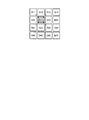
- FIG. 13 is a diagram illustrating another example of a configuration method of a color image sensor.
- the pixel corresponding to B22 shown in FIG. 13 has only B output, but the average value of the four pixels R11, R13, R31, and R33 is the average value of the four pixels R22, G12, G23, G32, and G21. Is calculated as G22, and is output as R, G, B of the pixel corresponding to B22. Further, the pixel corresponding to G23 shown in FIG.
- the average value of the two neighboring pixels R13 and R33 is calculated as the average value of two pixels R23, B22 and B24 as B23, Assume that R, G, and B of the pixel corresponding to G23 are output.
- Example 2 similarly to the pixel configuration method of the color image sensor, the pixels of the multi-polarization image sensor are configured. That is, the method of replacing each color filter of the R, G, B Bayer arrangement with each polarizing plate of 0 °, 45 °, 90 °, and 135 ° is the same as that of the first embodiment. Other points are the same as those in the first embodiment.
- each unit illustrated in the first and second embodiments can be changed or omitted without departing from the technical scope of the imaging apparatus according to the disclosed technology.
- Examples 1 and 2 are merely examples, and other modes in which various modifications and improvements are made based on the knowledge of those skilled in the art including the modes described in the disclosure section of the invention are also included in the disclosed technology. included.
Landscapes
- Physics & Mathematics (AREA)
- Engineering & Computer Science (AREA)
- General Physics & Mathematics (AREA)
- Multimedia (AREA)
- Signal Processing (AREA)
- Spectroscopy & Molecular Physics (AREA)
- Theoretical Computer Science (AREA)
- Optics & Photonics (AREA)
- Computer Security & Cryptography (AREA)
- Computer Hardware Design (AREA)
- Software Systems (AREA)
- General Engineering & Computer Science (AREA)
- Image Input (AREA)
- Studio Devices (AREA)
- Measurement Of The Respiration, Hearing Ability, Form, And Blood Characteristics Of Living Organisms (AREA)
Abstract
撮像装置(100)において、画像センサ(120)は、撮像対象の各点と対応する、複数の画素を含む画素グループの画素毎に偏光方向が異なるように設けられた偏光板を透して撮像対象を撮像する。画像取得部(110b)は、撮像対象へランダム偏光の照明光を照射する発光素子(130)をオフに制御した状態で画像センサ(120)により撮像対象を撮像した第1の画像を取得する。また、画像取得部(110b)は、第1の画像及び発光素子(130)をオンに制御した状態で画像センサ(120)により撮像対象を撮像した第2の画像の差分画像を取得する。画素選択部(110c)は、第1の画像又は差分画像の輝度に応じて、第1の画像又は差分画像のいずれかの一方の画像の各点と対応する画素グループ毎に最小輝度の画素を選択する。画像出力部(110d)は、画素選択部(110c)により選択された画素から生成した撮像対象の撮像画像を出力する。
Description
本発明は、撮像装置及び撮像方法に関する。
近年、生体認証が普及してきている。生体認証は、コンピュータ等の操作者が正当な操作者であるか否かの認証、例えば店舗における入出金装置の操作者の認証に用いられる。このような場合に、撮像装置は、例えば個人の手のひらの静脈を撮像する。撮像装置により撮像された画像に基づく静脈パターンが、予め登録された静脈パターンと一致する場合に、個人が認証される。入出金装置は、生体認証された操作者のみの操作を受け付ける。
生体認証を含む各用途の撮像装置は、撮像装置の撮像方向にかざされた手のひらに対して、赤外光を照射して撮像する。赤外光の一部は、手のひらの表面で反射するが、一部は表皮等を透過して手の内部の静脈のヘモグロビンで吸収される。このため、赤外光感度がある画像センサで撮像することにより、手のひらの表面情報に加えて、手のひらの内部の静脈パターンを取得することができる。
例えば、かかる撮像装置は、赤外光を照射する自己照明装置を有し、リング状導光体を通して手のひらに均一な光を照射し、レンズと画像センサからなる撮像系で手のひら画像を取得する。取得した手のひらの画像には、天井や壁等の背景も映り込んでおり、条件によっては画像処理段階で手のひらの切り出しや静脈パターンの信号抽出に悪影響を及ぼしたりする場合がある。
そのため、実際には、自己照明装置の点灯及び消灯の2条件下で撮像し、その差分画像を手のひら画像として使う方法が用いられる。自己照明装置のオン時及びオフ時の各画像には同一の背景が存在しており、その差分画像において、背景がキャンセルされ、手のひらのみの画像が得られる。
ここで、太陽光や室内灯等の環境光は、背景を照明するだけでなく、自己照明装置と共に手のひらも照明する。かかる環境光や外光による手のひらの照明も、静脈パターンの信号抽出に悪影響を及ぼす可能性があるが、差分画像によりキャンセルされ、自己照明装置にのみ照明された画像が得られる(例えば、特許文献1参照)。
しかしながら、上記技術では、屋外等のように外光が強い場合に、耐外光強度に限界があり、以下に説明するような問題がある。
精度よい差分画像を取得するためには、自己照明装置のオン時及びオフ時の各画像における手のひら部分の輝度が飽和していないことが条件となるが、例えば、外光が強くなってくると、手のひら画像の輝度のうち、自己照明装置による照明の寄与比率に対する外光による照明の寄与比率が大きくなる。そこで、画像が飽和しないように、自己照明装置のオン時及びオフ時の各画像の撮像の際の露出を同様に下げていくことになるが、それに伴って自己照明装置のオン時及びオフ時の各画像の差分が小さくなってしまい、精度よく静脈パターンを抽出することが困難になる。そのため、使用環境として外光強度に制限が設けられ、例えば屋外で使用する際には人為的な日陰となるような適切なカバーを用いる等の対策を行わなければならないという問題がある。
また、外光強度が高い場合には、外光のみを照明として用いることも考えられるが、外光の手のひらへの入射角度によっては局所的な高輝度領域(ハレーション等)が生じ、静脈パターンの信号抽出に悪影響を及ぼす可能性がある。よって、精度よく静脈パターンを抽出することが困難になるという問題がある。
開示の技術は、上記に鑑みてなされたものであって、例えば精度よく静脈パターンを抽出することができる撮像装置及び撮像方法を提供することを目的とする。
開示の技術の一例では、撮像装置は、画像センサ、画素選択部、画像出力部を有する。画像センサは、撮像対象の各点と対応する、複数の画素を含む画素グループの画素毎に偏光方向が異なるように設けられた偏光板を透して撮像対象を撮像する。画素選択部は、各点と対応する画素グループ毎に最小輝度の画素を選択する。画像出力部は、画素選択部により選択された画素から生成した撮像対象の撮像画像を出力する。
開示の技術の一例によれば、例えば精度よく静脈パターンを抽出することができる。
以下に添付図面を参照して本願に係る実施例について説明する。なお、以下の各実施例は、人の静脈の特徴から人を認証する静脈認証装置に適用される撮像装置を例に説明するが、開示の技術を限定するものではない。そして、開示の技術は、例えば差分画像から対象の生体情報を取得する撮像装置一般に適用可能である。そして、各実施例は、矛盾しない範囲で適宜組み合わせることが可能である。また、各実施例において、同一の構成及び処理には同一の符号を付与し、既出の構成及び処理の説明は省略する。
(実施例1に係る撮像装置)
以下、図1~図5Bを参照して、実施例1に係る撮像装置について説明する。図1は、実施例1に係る撮像装置の一例を示すブロック図である。図2Aは、実施例1に係る撮像装置の一例を示す斜視図である。図2Bは、実施例1に係る撮像装置の一例を示すI-I断面図である。
以下、図1~図5Bを参照して、実施例1に係る撮像装置について説明する。図1は、実施例1に係る撮像装置の一例を示すブロック図である。図2Aは、実施例1に係る撮像装置の一例を示す斜視図である。図2Bは、実施例1に係る撮像装置の一例を示すI-I断面図である。
図1に示すように、実施例1に係る撮像装置100は、マイクロコンピュータ等の処理装置である制御部110、画像センサ120、発光素子130を有する。図2Aに示すように、撮像装置100は、筐体100aに撮像ユニット1が収容され、赤外光に対して透光性を有するカバー100bにより覆蓋されている。撮像装置100は、カバー100bの上方からかざされた手のひらを撮像する。
図2Bに、図2AのI-I断面図を示すように、撮像装置100の撮像ユニット1は、基板2上に、画像センサ120、発光素子130、レンズユニット3、導光体4を有し、制御基板5上に制御部110を有する。発光素子130が出射する光は、導光体4を透して照明光としてカバー100bから上方へ出射される。この光は、カバー100bの上方からかざされた手のひらを照明し、手のひらにおいて反射又は吸収される。画像センサ120は、レンズユニット3のレンズを透して、カバー100bの上方からかざされた手のひらの画像を撮像する。
画像センサ120は、例えば偏光方向が異なる偏光板がそれぞれ設けられた4つのイメージセンサ毎で1つの画素を構成するマルチ偏光イメージセンサである。以下、画像センサ120における画素構成方法について説明する。マルチ偏光イメージセンサは、カラーイメージセンサと同様の考え方により構成され、カラーイメージセンサのカラーフィルタを偏光板に置き換えたものである。
図3Aは、カラーイメージセンサの構成の一例を示す図である。例えば図3Aに示すように、R(Red),G(Green),B(Blue)の各三原色に対応するカラーイメージセンサがベイヤー配列にて配置される。図3Aに示す配置パターンは、カラーイメージセンサのセンサ領域で繰り返される。
図3Bは、実施例1に係る撮像装置におけるマルチ偏光イメージセンサの構成の一例を示す図である。実施例1では、図3Aに示すカラーイメージセンサの構成方法をベースに、マルチ偏光イメージセンサを構成する。図3AのBの画素を格子の方向が0°の偏光板が設けられた画素に置き換える。同様に、図3Aに示す右上側のGの画素を格子の方向が45°の偏光板が設けられた画素に置き換える。同様に、図3AのRの画素を格子の方向が90°の偏光板が設けられた画素に置き換える。同様に、図3Aに示す左下側のGの画素を格子の方向が135°の偏光板が設けられた画素に置き換える。
なお、ここではワイヤーグリッド型の偏光板を想定しており、各偏光板の偏光光の透過方向及び反射方向は、図3Bに示すとおり、偏光の方向が格子の方向と直交する場合に透過し、偏光の方向と格子の方向が一致する場合には反射するものとする。格子の方向で透過または反射する偏光方向が決まるので、本明細書では格子の方向という用語の替りに偏光板の偏光方向という用語も使用することにする。また、原理的には吸収型の偏光板を用いることも可能であり、その場合は上述の反射は吸収に置き換わる。
このようにして、図3Bに示すように、4つの画素それぞれに偏光方向が異なる偏光板を設け、カラーイメージセンサと同様、この配列をセンサ領域全体で繰り返すことによりマルチ偏光イメージセンサを構成する。
図4は、カラーイメージセンサの画素構成方法の一例を示す図である。カラーイメージセンサでは、4つの異なる性質の画素で1つの画素を表す。図4に示すように、左上の破線囲み部分11の中にはRとBが1つずつ、Gが2つ含まれているが、これで1つの画素を構成すると考える。Gの出力は、2つのGの出力の平均値とする。次に、1列だけ右にずれた破線囲み部分12を1つ右の画素と考える。破線囲み部分12は、破線囲み部分11と比べると、Gの1つとBは共通であるが、もう一つのGとRは別のものを用いる。このようにして、図4における横方向の画素を構成する。同様に、図4における縦方向の画素が構成される。
マルチ偏光イメージセンサも、カラーイメージセンサと同様に画素を構成する。図5A及び図5Bは、実施例1に係る撮像装置のマルチ偏光イメージセンサの画素構成方法の一例を示す図である。図5Aの破線囲いで示すように偏光方向0°,45°,90°,135°の4つで1つの画素を構成する。1つ右の画素は、図5Bのように1列右にずらした破線囲いで構成する。横方向及び縦方向も1つずつ画素構成をずらすことによって、カラーイメージセンサと同様に出力画素数を維持したまま4方向の偏光特性を持った画像を取得することができる。
ここで実施例1の機能、効果を説明するために、まず撮像対象からの反射光の振る舞いについて説明する。図6A及び図6Bは、実施例1に係る撮像装置における撮像対象からの反射光の振る舞いの一例を示す図である。外光照明時の手のひら画像には、局所的高輝度領域により輝度のダイナミックレンジが拡大し、全体に信号レベルが下がったり、局所的高輝度領域に隠れて微小信号が消失したりして、手のひら認証に悪影響が生じる。局所的高輝度領域の発生は、照明光が手のひら表面で正反射して画像に乗ることが主因である。また、外光照明はランダム偏光であるが、物体表面で正反射する光の成分はS偏光成分が強くなるという偏りをもつ。
図6Aに示すように、対象物に入射した光は対象物の表面で反射するだけでなく、対象物の内部に浸透して散乱、反射を繰り返して表面から出てくるという形でも反射する。内部に浸透した光は、図6Aに示すように、人の皮膚組織内で散乱、反射を繰り返して表面から出射するが、指向性がほとんどなく、等方的に拡散する。
また、図6Bに示すように、物体表面の微細な凹凸でも光は様々な方向に反射する拡散反射となる。拡散反射は、反射を繰り返すので偏光方向も乱れ、仮に入射光が直線偏光であったとしても拡散反射される光はランダムになる。拡散反射の他、一部の光は物体の表面で正反射(鏡面反射)する。拡散反射と違い、正反射は鏡面反射の方向に強い指向性をもつ。
また、正反射光は、偏光特性にも特徴がある。物体表面での光の反射率は偏光方向で異なり、入射面内で電場が振動しているP偏光は界面を透過しやすく反射率が低い。また、電場の振動が入射面に垂直、すなわち界面に平行なS偏光は反射率が高い。そのため、入射光がランダム偏光であっても、正反射光はS偏光成分の強い光となる。この現象、すなわち物体表面における正反射と偏光方向の変化を図7に斜視図で示す。
図7に示すように、正反射の偏光方向は、物体表面の法線と入射光の方向で決まる入射面に対し、電場が垂直に振動するS偏光が強い。図8は、正反射と偏光方向の関係を物体表面の法線方向から見た平面図で模式的に表した図である。上述のように、物体表面で正反射する光の偏光方向は主にS偏光、すなわち入射面に垂直な方向である。したがって、ランダム偏光の照明光が図8の(A)の方向から入射する場合、物体表面で正反射する光の偏光方向は主に90°となる。同様に、方向(B)から入射した照明光の正反射は主に45°、方向(C)から入射した照明光の正反射は主に135°となる。
照明の入射方向が変わっても、常にその方向に対するS偏光を遮断する偏光板を用いることができれば、太陽光などのランダム偏光の照明光であっても、その正反射光を大幅に減らすことが可能になる。
実施例1は、マルチ偏光イメージセンサの隣接する4つの画素が異なる方向の偏光を透過することを利用し、この正反射光を実用上十分なレベルまで排除するという機能を実現している。これによって、ランダム偏光であって入射方向の制御ができない外光照明を利用する場合でも、局所的高輝度領域のない、良好な手のひら画像を取得することができるという効果を期待することができる。
図9は太陽光のような強い外光で照明した場合の手のひらを示し、ここでは、レンズユニット3によって画像センサ120のセンサ面上に結像した光を表している。すなわち、図9の手のひら像は、画像センサ120への入力信号であり、この光がマルチ偏光イメージセンサの偏光板で強度変調を受け、画像センサ120の画素信号に変換される。
例えば、外光照明光が、手のひらに対して図9の方向(B)から入射し、手のひら画像の右下部に局所的高輝度領域が生じている場合、図3Bに示すマルチ偏光イメージセンサ4つの異なる偏光方向のうち、135°の方向の偏光板が正反射光を多く透過させ、画素の輝度が大きくなる。次に0°,90°の方向が大きく、右下からの正反射光を最も強く反射して透過量が少ない45°方向の画素の輝度が最も小さい。また、右下部の局所的高輝度領域を形成する外光照明が、図16の方向(A)から入射している場合には、マルチ偏光イメージセンサの4つの異なる偏光方向のうち、90°方向の偏光板が正反射光を最も強く反射して透過させない。すなわち、90°方向の偏光板を透過した光の強度は最も小さく、ほぼ拡散反射光であると考えられる。
このように、4画素1組で、最も小さい輝度の画素を採用するというルールで全ての画素を選べば、正反射を排除した良好な手のひら画像が取得できる。
説明を図1,図2A,図2Bに戻す。発光素子130は、LED(Light Emitting Diode)等の、撮像装置100にかざされた撮像対象の手のひらへランダム偏光光を照射する光源である。以下、発光素子130を、自己照明と呼ぶ場合がある。これに対し、太陽光や室内灯等の環境光を、外光照明と呼ぶ場合がある。また、自己照明光及び外光照明光を、照明光と総称する場合がある。
制御部110は、点灯制御部110a、画像取得部110b、画素選択部110c、画像出力部110dを有する。点灯制御部110aは、発光素子130の点灯及び消灯を制御する。
画像取得部110bは、点灯制御部110aに対して発光素子130の消灯を指示する。そして、画像取得部110bは、発光素子130が消灯された状態で、画像センサ130に、撮像装置100にかざされた手のひら及び背景を含む画像(以下、外光画像と呼ぶ場合がある)を撮像させることで取得する。外光は、屋外における自然光や屋内における屋内照明光等、自己照明以外による光である。
また、画像取得部110bは、点灯制御部110aに対して発光素子130の点灯を指示する。そして、画像取得部110bは、発光素子130が点灯された状態で、画像センサ130に、撮像装置100にかざされた手のひら及び背景を含む画像(以下、自己照明画像と呼ぶ場合がある)を撮像させることで取得する。
そして、画像取得部110bは、外光画像と自己照明画像との差分画像を取得する。
画像取得部110bは、外光画像の所定部分(例えば画像の中心部分)の輝度が第1閾値以上、又は、外光画像と自己照明画像との差分画像の所定部分(例えば画像の中心部分)の輝度が第2閾値未満であるか否かを判定する。画像取得部110bは、外光画像の所定部分の輝度が第1閾値以上、又は、外光画像と自己照明画像との差分画像の所定部分の輝度が第2閾値未満である場合、外光画像を画素選択の処理対象画像とする。
一方、画像取得部110bは、外光画像の所定部分の輝度が第1閾値未満であって、外光画像と自己照明画像との差分画像の所定部分の輝度が第2閾値以上である場合、差分画像を画素選択の処理対象画像とする。なお、画像取得部110bは、外光画像の所定部分の輝度が第1閾値未満であっても、外光画像と自己照明画像との差分画像の所定部分の輝度が第2閾値未満である場合、外光画像を画素選択の処理対象画像とする。
画素選択部110cは、処理対象画像の画素のうち、隣接する4つの画素を1グループとした画素グループ毎に輝度が最小である画素を選択する。隣接する4つの画素とは、4つの画素を格子状に並べたものをいう。画像出力部110dは、画素選択部110cにより選択された画素をつなげて1つの手のひら画像を生成する。
(正反射を含む画像の輝度分布)
図10は、実施例1に係る撮像装置における撮像対象からの反射光のうち正反射を含む画像の輝度分布の一例を示す図である。図10の上方の手のひらを表す図における右下の正反射領域は、図10の下方に示す輝度分布のグラフにおいて局所的に輝度が高くなっている。
図10は、実施例1に係る撮像装置における撮像対象からの反射光のうち正反射を含む画像の輝度分布の一例を示す図である。図10の上方の手のひらを表す図における右下の正反射領域は、図10の下方に示す輝度分布のグラフにおいて局所的に輝度が高くなっている。
図10に示すように、手のひら画像全体の輝度分布は、拡散反射光によって作られた信号画像の上に、レンズに入射してきた正反射の光による局所的高輝度が重畳されたものである。したがって、正反射を排除すれば、拡散反射光による連続した画像が取得できることになる。4つの偏光方向の輝度出力のうち、最小の値を採用することにより、ランダム偏光照明による正反射光を大幅に削減することができ、1つの画像内における輝度分布の偏りの不都合を低減し、画像データにおける画素の連続性を十分に期待できる。
(実施例1に係る自己照明から外光照明への切り替え)
図11Aは、実施例1に係る撮像装置において強外光下での自己照明装置オンの場合の画像の輝度分布の一例を示す図である。図11Bは、実施例1に係る撮像装置において強外光下での自己照明装置オフの場合の画像の輝度分布の一例を示す図である。図11Cは、実施例1に係る撮像装置において強外光下での自己照明装置オン及びオフの場合の差分画像の輝度分布の一例を示す図である。図11A~図11Cを参照して、実施例1に係る自己照明から外光照明への切り替えについて説明する。
図11Aは、実施例1に係る撮像装置において強外光下での自己照明装置オンの場合の画像の輝度分布の一例を示す図である。図11Bは、実施例1に係る撮像装置において強外光下での自己照明装置オフの場合の画像の輝度分布の一例を示す図である。図11Cは、実施例1に係る撮像装置において強外光下での自己照明装置オン及びオフの場合の差分画像の輝度分布の一例を示す図である。図11A~図11Cを参照して、実施例1に係る自己照明から外光照明への切り替えについて説明する。
屋内等の、外光の強度が高くない場合は、図11Bに示す破線のように、自己照明OFFの画像の輝度は低く、よって、外光画像と自己照明画像との差分画像も、図11Cに示す破線のように、輝度に十分な差分が生じる画像となる。しかし、外光の強度の高い環境になると、外光画像と自己照明画像との差分画像は、図11Bに示す実線のように、自己照明OFFの画像の輝度が高くなり、図11Cに示す実線のように、輝度に十分な差分が出ない画像となる。
具体的には、外光の強度が上がると、図11Aに示す自己照明ONの場合も、図11Bに示す自己照明OFFの場合も、いずれも輝度が高くなるため、輝度が飽和しないように露光時間を短縮することになる。そのため、外光画像と自己照明画像との差分画像の輝度差が小さくなるわけである。このように、輝度差が小さくなると、光や回路ノイズの影響が大きくなり、手のひらの静脈パターンの抽出の画像処理に悪影響が現れる。
そこで、実施例1では、閾値判定により、差分画像による手のひら静脈パターンの取得方法から、外光画像のみによる手のひら静脈パターンの取得方法に切り替える。具体的には、実施例1では、図11Bに示す外光画像の例えば中心部分の輝度が第1閾値以上になると、差分画像による手のひら静脈パターンの取得方法から、外光画像のみによる手のひら静脈パターンの取得方法に切り替える。または、実施例1では、図11Cに示す差分画像の輝度が第2閾値未満となると、差分画像による手のひら静脈パターンの取得方法から、外光画像のみによる手のひら静脈パターンの取得方法に切り替える。
すなわち、実施例1では、外光の強度が所定強度未満の屋内等では自己照明で手のひらを撮像する。そして、窓際や屋外での使用などにより外光強度が強くなってくると、自己照明ON及びOFFの差分画像取得のための適正露出時間が短くなってくる。このため、実施例1では、ある条件を境にして、差分画像による手のひら静脈パターンの取得方法から、外光画像のみによる手のひら静脈パターンの取得方法に切り替える。
(実施例1に係る撮像装置における撮像処理)
図12は、実施例1に係る撮像装置における撮像処理の一例を示すフローチャートである。図12に示すように、先ず、撮像装置100は、手のひらを撮像するか否かを判定する(ステップS11)。撮像装置100は、手のひらを撮像する場合(ステップS11:Yes)、ステップS12へ処理を移す。一方、撮像装置100は、手のひらを撮像しない場合(ステップS11:No)、ステップS11を繰り返す。
図12は、実施例1に係る撮像装置における撮像処理の一例を示すフローチャートである。図12に示すように、先ず、撮像装置100は、手のひらを撮像するか否かを判定する(ステップS11)。撮像装置100は、手のひらを撮像する場合(ステップS11:Yes)、ステップS12へ処理を移す。一方、撮像装置100は、手のひらを撮像しない場合(ステップS11:No)、ステップS11を繰り返す。
ステップS12では、撮像装置100は、自己照明をOFFにする。次に、撮像装置100は、手のひらの外光画像を取得する(ステップS13)。次に、撮像装置100は、外光画像(の例えば所定部分)の輝度が第1閾値以上であるか否かを判定する(ステップS14)。撮像装置100は、外光画像の(所定部分の)輝度が第1閾値以上である場合(ステップS14:Yes)、ステップS21へ処理を移す。一方、撮像装置100は、外光画像の(所定部分の)輝度が第1閾値未満である場合(ステップS14:No)、ステップS15へ処理を移す。
ステップS15では、撮像装置100は、自己照明をONにする。次に、撮像装置100は、自己照明画像を取得する(ステップS16)。次に、撮像装置100は、自己照明をOFFにする(ステップS17)。次に、撮像装置100は、ステップS13で取得した外光画像と、ステップS16で取得した自己照明画像との差分画像を取得する(ステップS18)。
次に、撮像装置100は、差分画像(の例えば所定部分)の輝度が第2閾値未満であるか否かを判定する(ステップS19)。撮像装置100は、差分画像(の例えば所定部分)の輝度が第2閾値未満である場合(ステップS19:Yes)、ステップS21へ処理を移す。一方、撮像装置100は、差分画像(の例えば所定部分)の輝度が第2閾値以上である場合(ステップS19:No)、ステップS20へ処理を移す。
ステップS20では、撮像装置100は、差分画像を処理対象画像とする。一方、ステップS21では、撮像装置100は、外光画像を処理対象画像とする。ステップS20又はステップS21が終了すると、撮像装置100は、ステップS22へ処理を移す。
ステップS22では、撮像装置100は、処理対象画像から画素グループ毎に最小輝度の画素を選択する。そして、撮像装置100は、ステップS22で選択した画素から出力画像を生成する(ステップS23)。次に、撮像装置100は、撮像処理を終了するか否かを判定する(ステップS24)。撮像装置100は、撮像処理を終了する場合(ステップS24:Yse)、撮像処理を終了し、撮像処理を終了しない場合(ステップS24:No)、ステップS11へ処理を移す。
なお、ステップS19において、差分画像(の例えば所定部分)の輝度が第2閾値未満である場合(ステップS19:Yes)には、撮像装置100は、ステップS21~ステップS24の処理を行わず、ステップS11へ処理を移すとしてもよい。あるいは判定をS14の第一閾値判定のみにしてS19の処理を削除してもよい。
あるいは、「外光画像」又は「自己照明画像」のいずれかの画像を取得すると、取得した画像に対して直ちにステップS22~ステップS23の処理を画素選択及び出力画像生成の処理を行い、他方の画像取得は行わないとしてもよい。
あるいは、ステップS12の自己照明OFFとステップS15の自己照明ONとを入れ替え、かつ、ステップS13の外光画像取得とステップS16の自己照明画像取得とを入れ替えてもよい。すなわち、「第1の画像」及び「第2の画像」のそれぞれが、「外光画像」及び「自己照明画像」であっても、「自己照明画像」及び「外光画像」であってもいずれでもよい。
実施例1では、外光を照明として利用しながらも、テカリ等の局所的な高輝度領域を除外した良好な手のひら画像を取得することができる。
なお、実施例1では、撮像装置100の制御部110が、図12のフローチャートに示す各種処理を行うとするが、これに限らず、撮像装置100と外部制御装置(図示せず)を接続し、外部制御装置が撮像装置100を制御して各種処理を行うとしてもよい。
実施例2は、画素構成方法において、図4に示すカラーイメージセンサの画素構成方法を基本とする実施例1と比較して、他の画素構成方法を基本とする。図13は、カラーイメージセンサの構成方法の他の一例を示す図である。図13に示すB22と対応する画素はBの出力しかないが、周囲のR11,R13,R31,R33の4つの画素の平均値をR22,G12,G23,G32,G21の4つの画素の平均値をG22として算出し、B22と対応する画素のR,G,Bの出力とする。また、図13に示すG23と対応する画素はGの出力しかないが、周囲のR13,R33の2つの画素の平均値をR23、B22,B24の2つの画素の平均値をB23として算出し、G23と対応する画素のR,G,Bの出力とする。
実施例2では、かかるカラーイメージセンサの画素構成方法と同様に、マルチ偏光イメージセンサの画素を構成する。すなわち、R,G,Bのベイヤー配列の各カラーフィルタを、0°,45°,90°,135°の各偏光板に置き換える方法は、実施例1と同様である。また、その他の点についても、実施例1と同様である。
なお、実施例1及び2以外の様々な公知の画素構成方法を、求められる画像品質によって使い分けて画素構成してもよい。
実施例1~2で例示した各部の構成は、開示の技術に係る撮像装置の技術範囲を逸脱しない程度に変更又は省略可能である。また、実施例1~2は例示に過ぎず、発明の開示の欄に記載の態様を始めとして、当業者の知識に基づいて種々の変形、改良を施した他の態様も、開示の技術に含まれる。
100 撮像装置
110 制御部
110a 点灯制御部
110b 画像取得部
110c 画素選択部
110d 画像出力部
120 画像センサ
130 発光素子
110 制御部
110a 点灯制御部
110b 画像取得部
110c 画素選択部
110d 画像出力部
120 画像センサ
130 発光素子
Claims (5)
- 撮像対象の各点と対応する、複数の画素を含む画素グループの画素毎に偏光方向が異なるように設けられた偏光板を透して前記撮像対象を撮像する画像センサと、
前記各点と対応する前記画素グループ毎に最小輝度の画素を選択する画素選択部と、
前記画素選択部により選択された画素から生成した前記撮像対象の撮像画像を出力する画像出力部と
を備えたことを特徴とする撮像装置。 - 撮像対象へランダム偏光の照明光を照射する発光素子と、
前記発光素子のオン及びオフを制御する点灯制御部と、
前記発光素子をオフに制御した状態で前記画像センサにより前記撮像対象を撮像した第1の画像、及び、該第1の画像と前記発光素子をオンに制御した状態で前記画像センサにより前記撮像対象を撮像した第2の画像との差分画像を取得する画像取得部と、をさらに備え、
前記画素選択部は、前記第1の画像又は前記差分画像の輝度に応じて、前記第1の画像又は前記差分画像のいずれか一方の画像の各点と対応する前記画素グループ毎に最小輝度の画素を選択する
ことを特徴とする請求項1に記載の撮像装置。 - 前記画像取得部は、前記第1の画像の輝度が第1閾値以上である場合には、前記第2の画像及び前記差分画像の取得をキャンセルし、
前記画素選択部は、前記第1の画像の各点と対応する前記画素グループ毎に最小輝度の画素を選択する
ことを特徴とする請求項2に記載の撮像装置。 - 前記画像取得部は、前記第1の画像の輝度が第1閾値未満である場合に、前記第2の画像及び前記差分画像を取得し、
前記画素選択部は、前記差分画像の輝度が第2閾値以上である場合に前記差分画像の各点と対応する前記画素グループ毎に最小輝度の画素を選択し、前記差分画像の輝度が第2閾値未満である場合に前記第1の画像の各点と対応する前記画素グループ毎に最小輝度の画素を選択する
ことを特徴とする請求項2に記載の撮像装置。 - 撮像装置が実行する撮像方法であって、
撮像対象の各点と対応する、複数の画素を含む画素グループの画素毎に偏光方向が異なるように設けられた偏光板を透して前記撮像対象を撮像する撮像ステップと、
前記各点と対応する前記画素グループ毎に最小輝度の画素を選択する画素選択ステップと、
前記画素選択ステップにより選択された画素から生成した前記撮像対象の撮像画像を出力する画像出力ステップと
を含んだことを特徴とする撮像方法。
Priority Applications (3)
| Application Number | Priority Date | Filing Date | Title |
|---|---|---|---|
| JP2018502875A JP6568301B2 (ja) | 2016-02-29 | 2016-02-29 | 撮像装置及び撮像方法 |
| PCT/JP2016/056095 WO2017149608A1 (ja) | 2016-02-29 | 2016-02-29 | 撮像装置及び撮像方法 |
| US16/052,019 US10970802B2 (en) | 2016-02-29 | 2018-08-01 | Imaging device and imaging method selecting a pixel having a lowest brightness |
Applications Claiming Priority (1)
| Application Number | Priority Date | Filing Date | Title |
|---|---|---|---|
| PCT/JP2016/056095 WO2017149608A1 (ja) | 2016-02-29 | 2016-02-29 | 撮像装置及び撮像方法 |
Related Child Applications (1)
| Application Number | Title | Priority Date | Filing Date |
|---|---|---|---|
| US16/052,019 Continuation US10970802B2 (en) | 2016-02-29 | 2018-08-01 | Imaging device and imaging method selecting a pixel having a lowest brightness |
Publications (1)
| Publication Number | Publication Date |
|---|---|
| WO2017149608A1 true WO2017149608A1 (ja) | 2017-09-08 |
Family
ID=59742635
Family Applications (1)
| Application Number | Title | Priority Date | Filing Date |
|---|---|---|---|
| PCT/JP2016/056095 Ceased WO2017149608A1 (ja) | 2016-02-29 | 2016-02-29 | 撮像装置及び撮像方法 |
Country Status (3)
| Country | Link |
|---|---|
| US (1) | US10970802B2 (ja) |
| JP (1) | JP6568301B2 (ja) |
| WO (1) | WO2017149608A1 (ja) |
Cited By (5)
| Publication number | Priority date | Publication date | Assignee | Title |
|---|---|---|---|---|
| WO2019176237A1 (ja) * | 2018-03-14 | 2019-09-19 | ソニーセミコンダクタソリューションズ株式会社 | 静脈認証システムおよび電子機器 |
| JP2020166761A (ja) * | 2019-03-29 | 2020-10-08 | シャープ株式会社 | 撮像装置、およびその制御方法 |
| WO2023043045A1 (ko) * | 2021-09-17 | 2023-03-23 | 삼성전자주식회사 | 전기 변색 소자를 포함하는 전자 장치 및 그 제어 방법 |
| WO2023189599A1 (ja) * | 2022-03-28 | 2023-10-05 | 株式会社小糸製作所 | 距離画像センサ、および車両用灯具 |
| US12474615B2 (en) | 2021-09-17 | 2025-11-18 | Samsung Electronics Co., Ltd. | Electronic device including electrochromic device and method of controlling the electronic device |
Families Citing this family (4)
| Publication number | Priority date | Publication date | Assignee | Title |
|---|---|---|---|---|
| WO2020010353A1 (en) * | 2018-07-06 | 2020-01-09 | Polaris Sensor Technologies Inc | Reducing glare for objects viewed through transpatent surfaces |
| US10924645B2 (en) | 2018-11-29 | 2021-02-16 | Microsoft Technology Licensing, Llc | Polarization imaging to detect display screen |
| US11050944B2 (en) | 2018-11-29 | 2021-06-29 | Microsoft Technology Licensing, Llc | Switched polarization imaging to detect display screen |
| CN112069475B (zh) * | 2020-09-14 | 2023-10-24 | 杭州领信数科信息技术有限公司 | 一种身份安全管理系统 |
Citations (3)
| Publication number | Priority date | Publication date | Assignee | Title |
|---|---|---|---|---|
| JPH1141514A (ja) * | 1997-07-17 | 1999-02-12 | Nippon Hoso Kyokai <Nhk> | 映り込み防止形撮像装置 |
| WO2008099589A1 (ja) * | 2007-02-13 | 2008-08-21 | Panasonic Corporation | 画像処理システム、方法、装置、及び画像フォーマット |
| JP2012173916A (ja) * | 2011-02-21 | 2012-09-10 | Nippon Hoso Kyokai <Nhk> | 撮像装置および画像処理情報生成プログラム |
Family Cites Families (14)
| Publication number | Priority date | Publication date | Assignee | Title |
|---|---|---|---|---|
| JP3955616B2 (ja) * | 2005-09-01 | 2007-08-08 | 松下電器産業株式会社 | 画像処理方法、画像処理装置及び画像処理プログラム |
| JP5691669B2 (ja) * | 2011-03-08 | 2015-04-01 | 富士通株式会社 | 生体情報処理装置、生体情報処理方法、および生体情報処理プログラム |
| JP6017072B2 (ja) * | 2011-12-16 | 2016-10-26 | Jfeケミカル株式会社 | 非晶質炭素粒子の製造方法 |
| WO2013114888A1 (ja) * | 2012-02-02 | 2013-08-08 | パナソニック株式会社 | 撮像装置 |
| JP2014078857A (ja) * | 2012-10-10 | 2014-05-01 | Fujitsu Frontech Ltd | 撮像装置、撮像方法及び撮像プログラム |
| WO2015015717A1 (ja) * | 2013-07-30 | 2015-02-05 | パナソニックIpマネジメント株式会社 | 撮像装置、並びにそれを用いた撮像システム、電子ミラーシステムおよび測距装置 |
| US9645074B2 (en) * | 2014-02-06 | 2017-05-09 | Panasonic Intellectual Property Management Co., Ltd. | Image processing apparatus |
| JP6485078B2 (ja) * | 2014-02-18 | 2019-03-20 | パナソニックIpマネジメント株式会社 | 画像処理方法および画像処理装置 |
| US9307159B2 (en) * | 2014-03-04 | 2016-04-05 | Panasonic Intellectual Property Management Co., Ltd. | Polarization image processing apparatus |
| JP6713472B2 (ja) * | 2015-01-22 | 2020-06-24 | ザ スクリプス リサーチ インスティテュート | クロメノンモノカルボン酸トランスポータ阻害薬 |
| US9824295B2 (en) * | 2016-02-18 | 2017-11-21 | L-3 Communications Cincinnati Electronics Corporation | Imaging systems and methods including obscurant characterization |
| US10521660B2 (en) * | 2016-04-28 | 2019-12-31 | Sharp Kabushiki Kaisha | Image processing method and image processing device |
| DE112017004203T5 (de) * | 2016-08-24 | 2019-06-13 | Sony Corporation | Bildverarbeitungsvorrichtung, informationserzeugungsvorrichtung und informationserzeugungsverfahren |
| EP3544283B1 (en) * | 2016-11-15 | 2023-07-19 | Sony Group Corporation | Image processing device |
-
2016
- 2016-02-29 JP JP2018502875A patent/JP6568301B2/ja active Active
- 2016-02-29 WO PCT/JP2016/056095 patent/WO2017149608A1/ja not_active Ceased
-
2018
- 2018-08-01 US US16/052,019 patent/US10970802B2/en active Active
Patent Citations (3)
| Publication number | Priority date | Publication date | Assignee | Title |
|---|---|---|---|---|
| JPH1141514A (ja) * | 1997-07-17 | 1999-02-12 | Nippon Hoso Kyokai <Nhk> | 映り込み防止形撮像装置 |
| WO2008099589A1 (ja) * | 2007-02-13 | 2008-08-21 | Panasonic Corporation | 画像処理システム、方法、装置、及び画像フォーマット |
| JP2012173916A (ja) * | 2011-02-21 | 2012-09-10 | Nippon Hoso Kyokai <Nhk> | 撮像装置および画像処理情報生成プログラム |
Cited By (5)
| Publication number | Priority date | Publication date | Assignee | Title |
|---|---|---|---|---|
| WO2019176237A1 (ja) * | 2018-03-14 | 2019-09-19 | ソニーセミコンダクタソリューションズ株式会社 | 静脈認証システムおよび電子機器 |
| JP2020166761A (ja) * | 2019-03-29 | 2020-10-08 | シャープ株式会社 | 撮像装置、およびその制御方法 |
| WO2023043045A1 (ko) * | 2021-09-17 | 2023-03-23 | 삼성전자주식회사 | 전기 변색 소자를 포함하는 전자 장치 및 그 제어 방법 |
| US12474615B2 (en) | 2021-09-17 | 2025-11-18 | Samsung Electronics Co., Ltd. | Electronic device including electrochromic device and method of controlling the electronic device |
| WO2023189599A1 (ja) * | 2022-03-28 | 2023-10-05 | 株式会社小糸製作所 | 距離画像センサ、および車両用灯具 |
Also Published As
| Publication number | Publication date |
|---|---|
| US10970802B2 (en) | 2021-04-06 |
| US20180336655A1 (en) | 2018-11-22 |
| JPWO2017149608A1 (ja) | 2018-06-07 |
| JP6568301B2 (ja) | 2019-08-28 |
Similar Documents
| Publication | Publication Date | Title |
|---|---|---|
| JP6568301B2 (ja) | 撮像装置及び撮像方法 | |
| US20220345644A1 (en) | Optical module having symmetrical opaque layer | |
| US10492660B2 (en) | Image processing apparatus and endoscope | |
| KR20220005600A (ko) | 언더-디스플레이 이미지 센서 | |
| CN111095284B (zh) | 指纹检测装置、方法和电子设备 | |
| JP5799264B2 (ja) | 画像処理装置および内視鏡 | |
| US9787907B2 (en) | Substance detection device | |
| JP3802892B2 (ja) | 虹彩認証装置 | |
| US20110298909A1 (en) | Image processing apparatus, image processing method, program and electronic apparatus | |
| US11068733B2 (en) | Biometric imaging system and method of determining properties of a biometric object using the biometric imaging system | |
| CN106233089A (zh) | 针对立体匹配的环境依赖的主动照明 | |
| CN114270803B (zh) | 相位检测自动聚焦(pdaf)传感器 | |
| JP2002191058A (ja) | 3次元画像取得装置および3次元画像取得方法 | |
| US20130100266A1 (en) | Method and apparatus for determination of object topology | |
| JP4747065B2 (ja) | 画像生成装置、画像生成方法および画像生成プログラム | |
| WO2004072899A1 (ja) | 成り済まし検出装置、および成り済まし検出方法 | |
| JP6775421B2 (ja) | 照明パターン形成を用いた計測光学系及び方法 | |
| EP3265765A1 (en) | Sensing images and light sources | |
| JP2022545334A (ja) | カメラのための光源 | |
| CN110574368B (zh) | 固态摄像装置、摄像系统以及物体识别系统 | |
| JP2002330336A5 (ja) | ||
| CN104054400B (zh) | 用于探测及控制编码光源的方法 | |
| KR101407818B1 (ko) | 텍스쳐 영상과 깊이 영상을 추출하는 장치 및 방법 | |
| US10458849B2 (en) | Sensor assembly for capturing spatially resolved photometric data | |
| US11070722B2 (en) | Image capturing device and control method |
Legal Events
| Date | Code | Title | Description |
|---|---|---|---|
| ENP | Entry into the national phase |
Ref document number: 2018502875 Country of ref document: JP Kind code of ref document: A |
|
| NENP | Non-entry into the national phase |
Ref country code: DE |
|
| 121 | Ep: the epo has been informed by wipo that ep was designated in this application |
Ref document number: 16892453 Country of ref document: EP Kind code of ref document: A1 |
|
| 122 | Ep: pct application non-entry in european phase |
Ref document number: 16892453 Country of ref document: EP Kind code of ref document: A1 |