WO2017142058A1 - 表面被覆切削工具 - Google Patents
表面被覆切削工具 Download PDFInfo
- Publication number
- WO2017142058A1 WO2017142058A1 PCT/JP2017/005848 JP2017005848W WO2017142058A1 WO 2017142058 A1 WO2017142058 A1 WO 2017142058A1 JP 2017005848 W JP2017005848 W JP 2017005848W WO 2017142058 A1 WO2017142058 A1 WO 2017142058A1
- Authority
- WO
- WIPO (PCT)
- Prior art keywords
- layer
- ticn
- compound
- cutting
- carbonitride
- Prior art date
- Legal status (The legal status is an assumption and is not a legal conclusion. Google has not performed a legal analysis and makes no representation as to the accuracy of the status listed.)
- Ceased
Links
Images
Classifications
-
- B—PERFORMING OPERATIONS; TRANSPORTING
- B23—MACHINE TOOLS; METAL-WORKING NOT OTHERWISE PROVIDED FOR
- B23B—TURNING; BORING
- B23B27/00—Tools for turning or boring machines; Tools of a similar kind in general; Accessories therefor
- B23B27/14—Cutting tools of which the bits or tips or cutting inserts are of special material
-
- C—CHEMISTRY; METALLURGY
- C23—COATING METALLIC MATERIAL; COATING MATERIAL WITH METALLIC MATERIAL; CHEMICAL SURFACE TREATMENT; DIFFUSION TREATMENT OF METALLIC MATERIAL; COATING BY VACUUM EVAPORATION, BY SPUTTERING, BY ION IMPLANTATION OR BY CHEMICAL VAPOUR DEPOSITION, IN GENERAL; INHIBITING CORROSION OF METALLIC MATERIAL OR INCRUSTATION IN GENERAL
- C23C—COATING METALLIC MATERIAL; COATING MATERIAL WITH METALLIC MATERIAL; SURFACE TREATMENT OF METALLIC MATERIAL BY DIFFUSION INTO THE SURFACE, BY CHEMICAL CONVERSION OR SUBSTITUTION; COATING BY VACUUM EVAPORATION, BY SPUTTERING, BY ION IMPLANTATION OR BY CHEMICAL VAPOUR DEPOSITION, IN GENERAL
- C23C16/00—Chemical coating by decomposition of gaseous compounds, without leaving reaction products of surface material in the coating, i.e. chemical vapour deposition [CVD] processes
- C23C16/22—Chemical coating by decomposition of gaseous compounds, without leaving reaction products of surface material in the coating, i.e. chemical vapour deposition [CVD] processes characterised by the deposition of inorganic material, other than metallic material
- C23C16/30—Deposition of compounds, mixtures or solid solutions, e.g. borides, carbides, nitrides
-
- C—CHEMISTRY; METALLURGY
- C23—COATING METALLIC MATERIAL; COATING MATERIAL WITH METALLIC MATERIAL; CHEMICAL SURFACE TREATMENT; DIFFUSION TREATMENT OF METALLIC MATERIAL; COATING BY VACUUM EVAPORATION, BY SPUTTERING, BY ION IMPLANTATION OR BY CHEMICAL VAPOUR DEPOSITION, IN GENERAL; INHIBITING CORROSION OF METALLIC MATERIAL OR INCRUSTATION IN GENERAL
- C23C—COATING METALLIC MATERIAL; COATING MATERIAL WITH METALLIC MATERIAL; SURFACE TREATMENT OF METALLIC MATERIAL BY DIFFUSION INTO THE SURFACE, BY CHEMICAL CONVERSION OR SUBSTITUTION; COATING BY VACUUM EVAPORATION, BY SPUTTERING, BY ION IMPLANTATION OR BY CHEMICAL VAPOUR DEPOSITION, IN GENERAL
- C23C16/00—Chemical coating by decomposition of gaseous compounds, without leaving reaction products of surface material in the coating, i.e. chemical vapour deposition [CVD] processes
- C23C16/22—Chemical coating by decomposition of gaseous compounds, without leaving reaction products of surface material in the coating, i.e. chemical vapour deposition [CVD] processes characterised by the deposition of inorganic material, other than metallic material
- C23C16/30—Deposition of compounds, mixtures or solid solutions, e.g. borides, carbides, nitrides
- C23C16/32—Carbides
-
- C—CHEMISTRY; METALLURGY
- C23—COATING METALLIC MATERIAL; COATING MATERIAL WITH METALLIC MATERIAL; CHEMICAL SURFACE TREATMENT; DIFFUSION TREATMENT OF METALLIC MATERIAL; COATING BY VACUUM EVAPORATION, BY SPUTTERING, BY ION IMPLANTATION OR BY CHEMICAL VAPOUR DEPOSITION, IN GENERAL; INHIBITING CORROSION OF METALLIC MATERIAL OR INCRUSTATION IN GENERAL
- C23C—COATING METALLIC MATERIAL; COATING MATERIAL WITH METALLIC MATERIAL; SURFACE TREATMENT OF METALLIC MATERIAL BY DIFFUSION INTO THE SURFACE, BY CHEMICAL CONVERSION OR SUBSTITUTION; COATING BY VACUUM EVAPORATION, BY SPUTTERING, BY ION IMPLANTATION OR BY CHEMICAL VAPOUR DEPOSITION, IN GENERAL
- C23C16/00—Chemical coating by decomposition of gaseous compounds, without leaving reaction products of surface material in the coating, i.e. chemical vapour deposition [CVD] processes
- C23C16/22—Chemical coating by decomposition of gaseous compounds, without leaving reaction products of surface material in the coating, i.e. chemical vapour deposition [CVD] processes characterised by the deposition of inorganic material, other than metallic material
- C23C16/30—Deposition of compounds, mixtures or solid solutions, e.g. borides, carbides, nitrides
- C23C16/34—Nitrides
-
- C—CHEMISTRY; METALLURGY
- C23—COATING METALLIC MATERIAL; COATING MATERIAL WITH METALLIC MATERIAL; CHEMICAL SURFACE TREATMENT; DIFFUSION TREATMENT OF METALLIC MATERIAL; COATING BY VACUUM EVAPORATION, BY SPUTTERING, BY ION IMPLANTATION OR BY CHEMICAL VAPOUR DEPOSITION, IN GENERAL; INHIBITING CORROSION OF METALLIC MATERIAL OR INCRUSTATION IN GENERAL
- C23C—COATING METALLIC MATERIAL; COATING MATERIAL WITH METALLIC MATERIAL; SURFACE TREATMENT OF METALLIC MATERIAL BY DIFFUSION INTO THE SURFACE, BY CHEMICAL CONVERSION OR SUBSTITUTION; COATING BY VACUUM EVAPORATION, BY SPUTTERING, BY ION IMPLANTATION OR BY CHEMICAL VAPOUR DEPOSITION, IN GENERAL
- C23C16/00—Chemical coating by decomposition of gaseous compounds, without leaving reaction products of surface material in the coating, i.e. chemical vapour deposition [CVD] processes
- C23C16/22—Chemical coating by decomposition of gaseous compounds, without leaving reaction products of surface material in the coating, i.e. chemical vapour deposition [CVD] processes characterised by the deposition of inorganic material, other than metallic material
- C23C16/30—Deposition of compounds, mixtures or solid solutions, e.g. borides, carbides, nitrides
- C23C16/36—Carbonitrides
Definitions
- the invention of the present application has excellent plastic deformation resistance that the hard coating layer has excellent even when the hard coating layer is subjected to cutting under high load and low speed conditions in which the hard coating layer easily causes plastic deformation.
- the present invention relates to a surface-coated cutting tool (hereinafter referred to as a coated tool) that exhibits excellent wear resistance over the use of the above.
- a coated tool a surface-coated cutting tool
- a substrate (hereinafter collectively referred to as a tool substrate) composed of a tungsten carbide (hereinafter referred to as WC) -based cemented carbide or titanium carbonitride (hereinafter referred to as TiCN) -based cermet.
- the lower layer is a Ti carbide (hereinafter referred to as TiC) layer, a nitride (hereinafter also referred to as TiN) layer, a carbonitride (hereinafter referred to as TiCN) layer, a carbon oxide (hereinafter referred to as TiCO).
- TiCNO carbonitride oxide
- Al 2 O 3 layer aluminum oxide layer
- a composite hard layer composed of a titanium compound inner layer including at least one titanium carbonitride layer and an aluminum oxide outer layer is coated on the surface of a WC-based cemented carbide substrate.
- at least one titanium carbonitride layer constituting the titanium compound inner layer is a TiCN layer in which a maximum peak by X-ray diffraction appears on the (220) plane
- the aluminum oxide outer layer is a ⁇ type Occurrence of abnormal damage due to exfoliation, wear, etc. by using an aluminum oxide layer that is mainly composed of crystals and has a maximum peak on the surface defined as 2.79 angstroms of ⁇ -Al 2 O 3 in ASTM. It has been proposed to prevent tooling and improve tool life.
- the TiCN layer is oriented in the (220) plane, the adhesion with the substrate or the underlying layer is increased, and peeling from the interface is less likely to occur. be able to. Further, on the TiCN layer oriented in the (220) plane, an oxidation in which a maximum peak appears on a plane mainly composed of ⁇ -type crystals and defined as a plane having a plane spacing of 2.79 ⁇ in ⁇ -Al 2 O 3 in ASTM. When the aluminum layer is coated, the surface of the ⁇ -Al 2 O 3 having an orientation of 2.79 angstroms between the surfaces is smooth and the surface of the coating layer is smooth, so that abnormal damage due to friction between the chips and the tool is less likely to occur.
- the aluminum oxide layer is resistant to abnormal damage and exhibits stable wear resistance.
- the inner layer has a multilayer structure having a titanium carbonitride layer having a thickness of 10 ⁇ m or more and having a columnar structure
- the outer layer is at least The layer includes an ⁇ -type aluminum oxide layer, and the orientation index TC (422) and TC (311) of the (422) plane and the (311) plane are both 1.3 or more and 3 or less for the titanium carbonitride layer.
- the peel resistance and wear resistance of the coated tool It has been proposed to improve crater resistance and breaking strength.
- the orientation index TC (422) and TC (311) of the titanium carbonitride layer are both 1.3 or more, and the structure is a columnar structure, so that the fracture resistance of the film can be improved even with a film thickness of 10 ⁇ m or more. It is possible to greatly improve the wear resistance, and the progress of wear due to chipping during cutting can be suppressed, and the welding of the work material during cutting is less likely to occur. Since the increase in stress can be prevented, the peel resistance is also greatly improved.
- Patent Document 3 discloses that in a coated tool in which a hard coating layer including at least one titanium carbonitride layer is formed on a substrate surface, an orientation index out of the texture coefficient TC (hkl) of the titanium carbonitride layer.
- TC (220) is the maximum
- the indentation hardness of the hardness reference piece is Hs
- the indentation hardness of the titanium carbonitride layer is Ht, (average value of Ht) / Hs ⁇ 3 and the titanium carbonitride layer
- the maximum value of the indentation hardness is Htmax and the minimum value is Htmin, (Htmax ⁇ Htmin) / (average value of Ht) ⁇ 0.5
- the crystal orientation of the titanium carbonitride layer is controlled, and the carbon It has been proposed to improve the wear resistance and fracture resistance of the coated tool by eliminating variations in the hardness of the titanium nitride layer.
- Japanese Laid-Open Patent Publication No. 8-300203 A) Japanese Patent No. 11-140647 (A) Japanese Patent No. 5729777 (B)
- the inventors of the present invention have a high load acting on the cutting edge, and even when the hard coating layer is used under a high load / low speed cutting process condition in which plastic deformation easily occurs, As a result of diligent research on the structure of the hard coating layer that is unlikely to cause abnormal damage, a hard coating layer including at least a Ti compound layer is formed on the surface of the tool base, and at least one TiCN layer is formed as the Ti compound layer.
- a hard coating layer including at least a Ti compound layer is formed on the surface of the tool base, and at least one TiCN layer is formed as the Ti compound layer.
- the TiCN layer is formed as a columnar vertically long structure having an aspect ratio of 5 or more, in addition to excellent plastic deformation resistance, it exhibits excellent wear resistance provided by the columnar vertically long structure. I found it.
- This invention is made
- A The hard coating layer is composed of one layer or two or more layers selected from a Ti carbide layer, a nitride layer, a carbonitride layer, a carbonate layer, and a carbonitride layer, and at least one of them Comprises a Ti compound layer composed of Ti carbonitride layers and having a total average layer thickness of 2 to 15 ⁇ m
- the coated tool of the present invention a hard coating layer including a Ti compound layer is formed on the tool base surface, the Ti compound layer includes at least one TiCN layer, and at least one of the TiCN layers has a (200) orientation degree. It consists of a high TiCN layer.
- the hard coating layer of the coated tool of the present invention includes a Ti compound layer (for example, a TiC layer, a TiN layer, a TiCN layer, a TiCO layer, and a TiCNO layer), and the Ti compound layer itself has excellent high-temperature strength, and the tool The adhesion strength with the substrate surface is excellent, but when the total average layer thickness of the Ti compound layer is less than 2 ⁇ m, the above effect cannot be sufficiently exhibited. On the other hand, when the total average layer thickness of the Ti compound layer exceeds 15 ⁇ m, it becomes easy to cause plastic deformation due to a high load acting at the time of cutting.
- a Ti compound layer for example, a TiC layer, a TiN layer, a TiCN layer, a TiCO layer, and a TiCNO layer
- the total average layer thickness of the lower layer made of the Ti compound layer is set to 2 to 15 ⁇ m.
- the Ti compound layer of the hard coating layer of the coated tool of the present invention includes at least one TiCN layer, and the layer is configured as a TiCN layer having (200) orientation. That is, for the crystal grains constituting the at least one TiCN layer, when the diffraction peak intensity from each lattice plane is measured by X-ray diffraction, the maximum diffraction peak intensity appears on the (200) plane (200) orientation
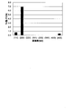
- FIG. 1 shows an example of a chart of diffraction peak intensity from each lattice plane measured by X-ray diffraction for the TiCN layer of the hard coating layer of the coated tool of the present invention. As is clear from FIG.
- the TiCN layer of the coated tool of the present invention shows the maximum peak intensity of the diffraction peak intensity for the (200) plane compared to the diffraction peak intensity from other lattice planes.
- X-ray diffraction was measured by the 2 ⁇ - ⁇ method using CuK ⁇ rays using a Spectris PANalytical Empire as an X-ray diffractometer, and measurement conditions (measurement range (2 ⁇ ): 30 to 130 degrees, X-ray output: The measurement was performed under the conditions of 45 kV, 40 mA, divergent slit: 0.5 degree, scan step: 0.013 degree, measurement time per step: 0.48 sec / step.
- the coated tool of the present invention has a value of Tc (200) of 2.0 or more, preferably 3.0 or more. It has the (200) orientation shown.
- the orientation index Tc (hkl) is defined by the following formula.
- I (hkl) represents the peak intensity (diffraction intensity) of the measured (hkl) plane
- I 0 (hkl) is a JCPDS card (Joint Committee on Powder Diffraction Standards (powder X-ray diffraction standard)).
- the average value of the powder diffraction intensity of TiC and TiN constituting the (hkl) plane represented is shown.
- (hkl) is the eight faces of (111), (200), (220), (311), (222), (331), (420), (422) Indicates the average value of 8 surfaces.
- At least one TiCN layer of the coated tool of the present invention shows the maximum peak intensity by X-ray diffraction on the (200) plane, and the orientation index Tc (200) ⁇ 2.0 (200). Due to the orientation, even when a large shearing force is applied to the TiCN layer during cutting, the TiCN layer has plastic deformation resistance. The occurrence of peeling or the occurrence of abnormal damage such as the progression of uneven wear can be suppressed, and the wear resistance can be improved thereby. However, when the X-ray diffraction peak intensity for the (200) plane cannot be said to be the maximum compared to the diffraction peak intensities from other lattice planes, or the orientation index Tc (200) is less than 4.0.
- the X-ray diffraction peak intensity of the (200) plane measured for at least one TiCN layer of the Ti compound layers is maximum as compared with the peak intensity of other crystal lattice planes.
- the orientation index Tc (200) was determined to be 2.0 or more, preferably 3.0 or more.
- At least one TiCN layer in the Ti compound layer has a columnar longitudinal structure.
- the area ratio occupied by columnar longitudinal TiCN crystal grains having an aspect ratio of 5 or more determined from the maximum grain width W of TiCN crystal grains and the maximum grain length L in the layer thickness direction is 70 areas of the longitudinal sectional area of the TiCN layer.
- the maximum grain width W and the maximum grain length L are the columnar vertically grown TiCN crystal grains, when one crystal grain in the longitudinal section of the TiCN layer is measured, the crystal grains in the direction perpendicular to the layer thickness direction.
- the largest value of the width (short side) is called the maximum particle width W, while the largest value of the crystal grain height (long side) in the layer thickness direction is called the maximum particle length L.
- the thickness of the TiCN layer is not particularly limited, but the thickness of all the TiCN layers constituting the Ti compound layer is preferably 4 to 13 ⁇ m. This indicates that when the thickness of the TiCN layer is 4 ⁇ m or more, the value of Tc (200) tends to increase, and the plastic deformation resistance in high-load cutting is improved, and the flank wear amount is also reduced, resulting in wear resistance. On the other hand, if the thickness of the TiCN layer exceeds 13 ⁇ m, plastic deformation is likely to occur, and abnormal damage due to the progress of uneven wear occurs.
- the lower Ti compound layer in this invention is formed as follows, for example. That is, various Ti compound layers comprising one or more of TiC layer, TiN layer, TiCN layer, TiCO layer, TiCNO layer and TiAlN layer are formed by vapor deposition using a normal chemical vapor deposition apparatus. Among them, a (200) highly oriented TiCN layer, or a TiCN layer in which columnar vertically elongated grains having an aspect ratio of 5 or more occupy 70 area% or more of the longitudinal section of the Ti compound layer, It can be formed by the following vapor deposition method.
- Reaction gas composition (volume%): TiCl 4 1-5%, CH 3 CN 0.5-1.5%, N 2 25-40%, balance H 2 , Reaction atmosphere temperature: 750 to 850 ° C.
- Reaction atmosphere pressure 5 to 10 kPa
- Reaction gas composition volume%: NH 3 0.5-2.0%, TiCl 4 0.1-0.3%, N 2 0-10%, balance H 2 , Reaction atmosphere temperature: 750 to 850 ° C.
- Reaction atmosphere pressure 5 to 8 kPa By creating under such conditions, it becomes easy to form crystal grains having a columnar longitudinal structure having an aspect ratio of 5 or more.
- the hard coating layer including the Ti compound layer formed on the surface of the tool base includes at least one TiCN layer as the Ti compound layer, and at least one of the TiCN layers.
- the two layers have a (200) orientation in which the maximum diffraction peak intensity due to X-ray diffraction appears on the (200) plane and the orientation index Tc (200) is 2.0 or more.
- Tc orientation index
- the area ratio of the crystal grains having a columnar longitudinal structure having an aspect ratio of 5 or more is 70 area% or more of the longitudinal section of the lower layer, whereby the wear resistance can be further improved. It is possible to extend the life of the cutting tool.
- Embodiments of the coated tool of the present invention will be specifically described based on examples.
- WC powder, TiC powder, ZrC powder, NbC powder, Cr 3 C 2 powder, TiN powder, and Co powder all having an average particle diameter of 1 to 3 ⁇ m were prepared. Then, after adding wax, ball mill mixing in acetone for 24 hours, drying under reduced pressure, press-molding into a green compact of a predetermined shape at a pressure of 98 MPa. In a vacuum, vacuum sintering is performed at a predetermined temperature within a range of 1370 to 1470 ° C. for 1 hour, and after sintering, a tool base a to WC-base cemented carbide having an ISO standard CNMG120408 insert shape is used. Each d was produced.
- ZrC powder ZrC powder
- TaC powder Mo 2 C powder
- WC powder Co powder all having an average particle diameter of 0.5 to 2 ⁇ m
- Ni powder these raw material powders are blended in the blending composition shown in Table 2, wet mixed by a ball mill for 24 hours, dried, and then pressed into a compact at a pressure of 98 MPa.
- the body was sintered in a nitrogen atmosphere of 1.3 kPa at a temperature of 1500 ° C. for 1 hour, and after sintering, a tool base e made of TiCN-based cermet having an insert shape of ISO standard CNMG120212 was produced.
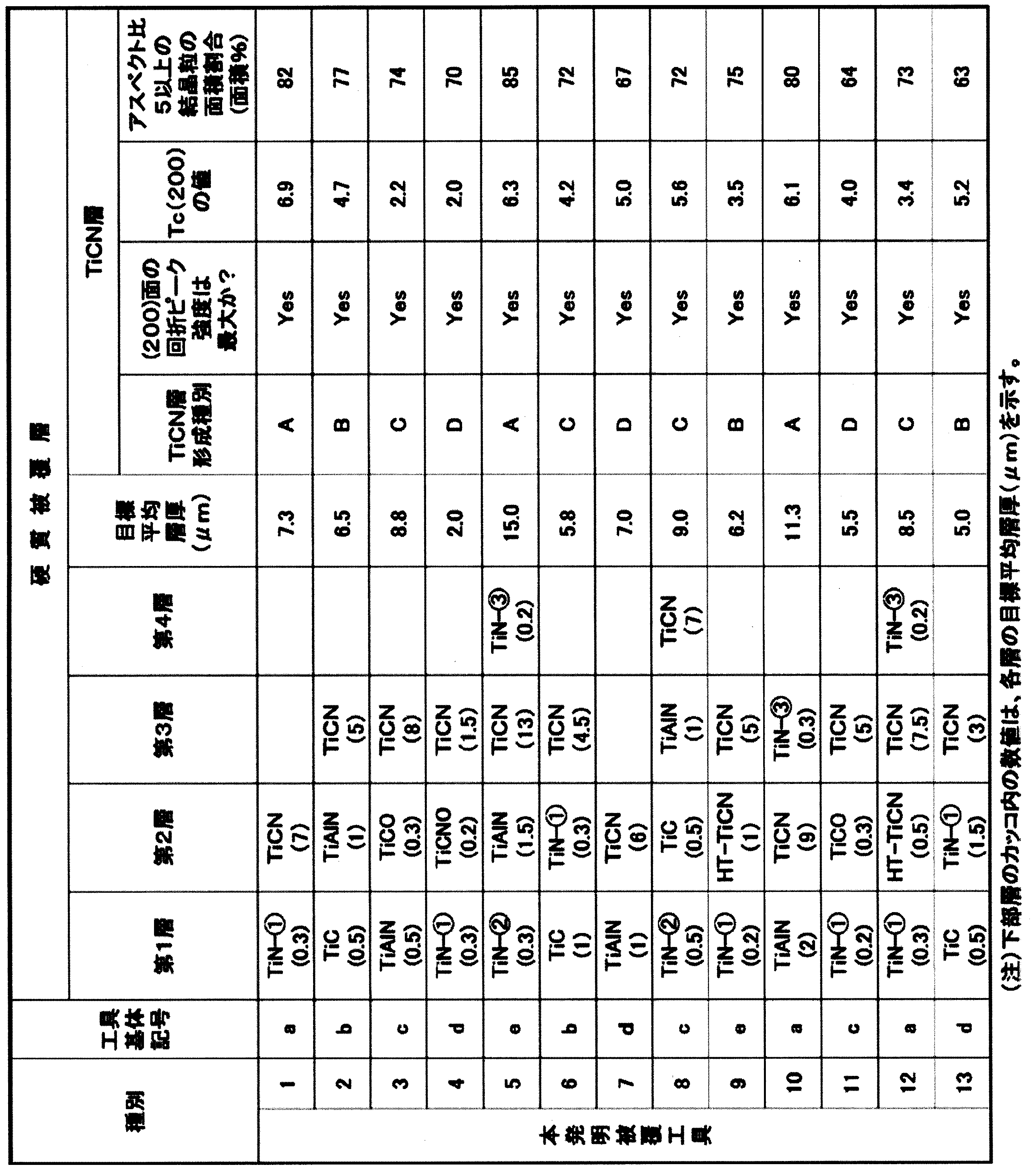
- each of the tool bases a to d and the tool base e is charged into a normal chemical vapor deposition apparatus, and a Ti compound layer having a target layer thickness shown in Table 6 under the conditions shown in Tables 3 and 4
- the coated tools 1 to 13 of the present invention shown in Table 6 were produced respectively by vapor deposition.
- the HT-TiCN layer shown in Table 3 is a TiCN layer manufactured at a higher reaction atmosphere temperature than the TiCN layer shown in paragraph 0016.
- the TiN layer-1 (first layer) and the TiAlN layer are the deposition conditions for the Ti compound layer in which columnar vertically oriented crystal grains having an aspect ratio of 5 or more are likely to be formed.
- each of the tool bases a to d and the tool base e is loaded into a normal chemical vapor deposition apparatus, and the target layer thicknesses shown in Table 7 are set under the conditions shown in Tables 3 and 5.
- Comparative example-coated tools 1 to 13 shown in Table 7 were produced by depositing a Ti compound layer.
- the diffraction peak intensity from each lattice plane was measured by X-ray diffraction.
- FIG. 1 the chart calculated
- X-ray diffraction was measured by the 2 ⁇ - ⁇ method using CuK ⁇ rays using Spectris PANalytical Empirean as an apparatus. Measurement conditions are measurement range (2 ⁇ ): 30 to 130 degrees, X-ray output: 45 kV, 40 mA, diverging slit: 0.5 degrees, scan step: 0.013 degrees, measurement time per step: 0.48 sec / step It is. From the chart obtained above, it was determined whether or not the diffraction peak intensity from the (200) plane was the maximum with respect to the diffraction peak intensities from other lattice planes. Tables 6 and 7 show the determination results.
- orientation index Tc (200) was determined based on the measurement result of the diffraction peak intensity.
- the orientation index Tc (200) was calculated by the following formula.
- I (hkl) represents the measured diffraction peak intensity of the (hkl) plane
- I 0 (hkl) is represented by a JCPDS card (Joint Committee on Powder Diffraction Standards (powder X-ray diffraction standard))
- hkl The average value of the powder diffraction intensities of TiC and TiN constituting the surface is shown.
- (hkl) is the eight surfaces (111), (200), (220), (311), (222), (331), (420), and (422).
- Tables 6 and 7 show the values of the orientation index Tc (200) calculated above.
- the longitudinal section of the TiCN layer of the lower layer of the coated tools 1 to 13 of the present invention and the comparative coated tools 1 to 13 is 10 ⁇ m in a direction parallel to the tool base using a scanning electron microscope (5000 times magnification).
- the maximum grain width W and the maximum grain length L are measured for each TiCN crystal grain existing in the region of the height of the TiCN layer in the direction perpendicular to the substrate, and the value of the aspect ratio L / W is set.
- the area ratio of crystal grains having an aspect ratio L / W of 5 or more in the longitudinal section of the TiCN layer was determined. Tables 6 and 7 show the area ratios obtained above.
- the thicknesses of the constituent layers of the hard coating layers of the inventive coated tools 1 to 13 and comparative example coated tools 1 to 13 were measured using a scanning electron microscope (longitudinal cross section measurement). The average layer thickness (average value of 5-point measurement) substantially the same as the thickness was shown.
- ⁇ Cutting condition B Work material: SUS304, Cutting speed: 200 m / min, Cutting depth: 2.0mm Feed: 0.3mm / rev, Cutting time: Dry interrupted cutting test of four stainless steel slit materials under conditions of 5 minutes. The flank wear width of the cutting edge in the above cutting test was measured, and the occurrence of abnormal damage such as chipping, chipping and peeling was observed with the naked eye. Tables 8 and 9 show the test results.
- the coated tools 1 to 13 of the present invention have a TiCN layer having excellent plastic deformation resistance as the Ti compound layer of the hard coating layer, the TiCN crystal grains fall off. Excellent wear resistance with no chipping, chipping or peeling caused by In contrast, the comparative example coated tools 1 to 13 have a relatively short service life due to abnormal damage such as dropping, chipping, chipping and peeling of TiCN crystal grains in high load / low speed cutting. It is clear that
- the coated tool of the present invention exhibits excellent cutting performance in high-load / low-speed cutting in which a high load (a large shearing force) acts on the cutting edge, but the normal conditions such as various steel and cast iron Of course, it can also be used for continuous cutting and intermittent cutting.
Landscapes
- Chemical & Material Sciences (AREA)
- Engineering & Computer Science (AREA)
- Mechanical Engineering (AREA)
- Inorganic Chemistry (AREA)
- General Chemical & Material Sciences (AREA)
- Chemical Kinetics & Catalysis (AREA)
- Materials Engineering (AREA)
- Metallurgy (AREA)
- Organic Chemistry (AREA)
- Cutting Tools, Boring Holders, And Turrets (AREA)
Abstract
工具基体表面に、硬質被覆層が形成されている表面被覆切削工具において、前記硬質被覆層は、TiC層、TiN層、TiCN層、TiCO層およびTiCNO層から選ばれる1層または2層以上からなり、その内の少なくとも1層はTiCN層で構成された2~15μmの合計平均層厚を有するTi化合物層を含み、該Ti化合物層中の少なくとも1層のTiCN層は、(200)面にX線回折による最大回折ピーク強度が現れ、かつ、配向性指数Tc(200)は2.0以上であり、好ましくは、Ti化合物層において、アスペクト比が5以上である柱状縦長組織を有する結晶粒が、Ti化合物層の縦断面に占める面積割合は、70面積%以上である表面被覆切削工具。
Description
本願発明は、各種の鋼や鋳鉄などの切削加工を、硬質被覆層が塑性変形を起こしやすい高負荷かつ低速条件で行った場合でも、硬質被覆層がすぐれた耐塑性変形性を有し、長期の使用に亘ってすぐれた耐摩耗性を発揮する表面被覆切削工具(以下、被覆工具という)に関する。
本願は、2016年2月17日に日本に出願された特願2016-027726号及び2017年2月16日に日本に出願された特願2017-026574号に基づき優先権を主張し、その内容をここに援用する。
本願は、2016年2月17日に日本に出願された特願2016-027726号及び2017年2月16日に日本に出願された特願2017-026574号に基づき優先権を主張し、その内容をここに援用する。
従来、一般に、炭化タングステン(以下、WCで示す)基超硬合金または炭窒化チタン(以下、TiCNで示す)基サーメットで構成された基体(以下、これらを総称して工具基体という)の表面に、
(a)下部層が、Tiの炭化物(以下、TiCで示す)層、窒化物(以下、同じくTiNで示す)層、炭窒化物(以下、TiCNで示す)層、炭酸化物(以下、TiCOで示す)層、および炭窒酸化物(以下、TiCNOで示す)層のうちの1層または2層以上からなるTi化合物層、
(b)上部層が、酸化アルミニウム層(以下、Al2O3層で示す)、
以上(a)および(b)で構成された硬質被覆層が蒸着形成された被覆工具が知られているが、被削材の種類、切削条件に応じて、耐チッピング性、耐欠損性、耐剥離性、耐摩耗性等の工具性能を高めるため、各種の提案がなされている。
(a)下部層が、Tiの炭化物(以下、TiCで示す)層、窒化物(以下、同じくTiNで示す)層、炭窒化物(以下、TiCNで示す)層、炭酸化物(以下、TiCOで示す)層、および炭窒酸化物(以下、TiCNOで示す)層のうちの1層または2層以上からなるTi化合物層、
(b)上部層が、酸化アルミニウム層(以下、Al2O3層で示す)、
以上(a)および(b)で構成された硬質被覆層が蒸着形成された被覆工具が知られているが、被削材の種類、切削条件に応じて、耐チッピング性、耐欠損性、耐剥離性、耐摩耗性等の工具性能を高めるため、各種の提案がなされている。
例えば、特許文献1には、WC基超硬合金基体の表面に、少なくとも1層のチタンの炭窒化物層を含むチタン化合物内層と、酸化アルミニウム外層とで構成された複合硬質層を被覆してなる切削工具において、前記チタン化合物内層を構成する少なくとも1層のチタンの炭窒化物層は、(220)面にX線回折による最大ピークが現れるTiCN層であり、前記酸化アルミニウム外層は、κ型結晶を主体とし、かつASTMにおいてκ-Al2O3の面間隔2.79オングストロームの面として定義される面に最大ピークが現れる酸化アルミニウム層とすることにより、剥離、摩耗等による異常損傷の発生を防止し、工具寿命の向上を図ることが提案されている。
即ち、TiCN層は(220)面に配向することで、基体または下の層との密着力を増し、界面からの剥離が起きにくくなるため、剥離に起因する異常損傷の発生や寿命低下を抑えることができる。また、(220)面に配向したTiCN層の上に、κ型結晶を主体としかつASTMにおいてκ-Al2O3の面間隔2.79オングストロームの面として定義される面に最大ピークが現れる酸化アルミニウム層を被覆すると、前記面間距離2.79オングストロームに配向性を示すκ-Al2O3は被覆層表面が平滑であるために、切り屑と工具間の摩擦による異常損傷が生じにくくなり、この酸化アルミニウム層が異常損傷を起しにくく安定した耐摩耗性を示すというものである。
即ち、TiCN層は(220)面に配向することで、基体または下の層との密着力を増し、界面からの剥離が起きにくくなるため、剥離に起因する異常損傷の発生や寿命低下を抑えることができる。また、(220)面に配向したTiCN層の上に、κ型結晶を主体としかつASTMにおいてκ-Al2O3の面間隔2.79オングストロームの面として定義される面に最大ピークが現れる酸化アルミニウム層を被覆すると、前記面間距離2.79オングストロームに配向性を示すκ-Al2O3は被覆層表面が平滑であるために、切り屑と工具間の摩擦による異常損傷が生じにくくなり、この酸化アルミニウム層が異常損傷を起しにくく安定した耐摩耗性を示すというものである。
また、特許文献2には、工具基体表面に内層および外層を被覆形成した被覆工具において、内層を10μm以上の厚みを有し柱状組織からなる炭窒化チタン層を有する多層構造とし、外層を、少なくともα型酸化アルミニウム層を含む層とし、前記炭窒化チタン層について、(422)面と(311)面との配向性指数TC(422)、TC(311)をともに1.3以上3以下とする配向性をもたせ、また、配向性指数TC(422)とTC(311)とを除く配向性指数TC(hkl)がすべて1.5以下とすることによって、被覆工具の耐剥離性、耐摩耗性、耐クレータ性、また、破壊強度を向上させることが提案されている。
ここで、炭窒化チタン層の配向性指数TC(422)、TC(311)をともに1.3以上とし、その組織を柱状組織とすることにより、10μm以上の膜厚でも膜の耐破壊性を大きく向上させ耐摩耗性を向上させることが可能となり、また、切削中のチッピングによる摩耗の進行が抑制し得るとともに、切削中の被削材の溶着が起こりにくくなり、その結果、膜にかかる切削応力の増大が防げることから耐剥離性も大幅に向上するとされている。
ここで、炭窒化チタン層の配向性指数TC(422)、TC(311)をともに1.3以上とし、その組織を柱状組織とすることにより、10μm以上の膜厚でも膜の耐破壊性を大きく向上させ耐摩耗性を向上させることが可能となり、また、切削中のチッピングによる摩耗の進行が抑制し得るとともに、切削中の被削材の溶着が起こりにくくなり、その結果、膜にかかる切削応力の増大が防げることから耐剥離性も大幅に向上するとされている。
また、特許文献3には、基体表面に、少なくとも1層の炭窒化チタン層を含む硬質被覆層を形成した被覆工具において、前記炭窒化チタン層の組織係数TC(hkl)のうちの配向性指数TC(220)を最大とし、また、硬度基準片の押し込み硬度をHsとし、炭窒化チタン層の押し込み硬度をHtとした場合、(Htの平均値)/Hs≧3、かつ、炭窒化チタン層の押し込み硬度の最大値をHtmax、最小値をHtminとした場合、(Htmax-Htmin)/(Htの平均値)<0.5とし、炭窒化チタン層の結晶配向性を制御するとともに、該炭窒化チタン層の硬度のばらつきをなくすことにより、被覆工具の耐摩耗性および耐欠損性の向上を図ることが提案されている。
近年の切削装置の高性能化はめざましく、一方で切削加工に対する省力化および省エネ化、さらに低コスト化の要求は強い。これに伴い、切削加工は一段と高能率化すると共に、高切り込みや高送りなどの重切削、断続切削等で切れ刃に高負荷が作用する傾向にある。前述した従来の被覆工具を鋼や鋳鉄などの通常の条件での連続切削、高速切削に用いた場合には問題はないが、従来の被覆工具を、高負荷が作用することにより、硬質被覆層が塑性変形を起こすような高負荷・低速切削加工条件に用いた場合には、硬質被覆層の塑性変形により、硬質被覆層を構成する結晶粒の脱落等が生じやすく、また、これに起因する異常摩耗が進行しやすく、これを原因として比較的短時間で工具寿命に至るという問題がある。
そこで、本願発明者らは、前述のような観点から、切れ刃に高負荷が作用し、硬質被覆層が塑性変形を起こしやすい高負荷・低速切削加工条件で使用した場合でも、硬質被覆層の異常損傷が発生しにくい硬質被覆層の構造について鋭意研究を行ったところ、工具基体表面に、少なくともTi化合物層を含む硬質被覆層を形成し、さらに、Ti化合物層として、少なくとも1層のTiCN層を含む層を形成し、該TiCN層の(200)配向性を高めた場合には、高負荷(特に、TiCN層表面への大きなせん断力)が作用したとしても、TiCN層がすぐれた耐塑性変形性を有するため、TiCN層を構成する結晶粒の脱落等による異常損傷の発生を抑制し得ること、また、これにより耐摩耗性の向上を図り得ることを見出したのである。
また、前記TiCN層を、アスペクト比が5以上である柱状縦長組織として形成した場合には、すぐれた耐塑性変形性に加え、柱状縦長組織によりもたらされる一段とすぐれた耐摩耗性を発揮することを見出したのである。
また、前記TiCN層を、アスペクト比が5以上である柱状縦長組織として形成した場合には、すぐれた耐塑性変形性に加え、柱状縦長組織によりもたらされる一段とすぐれた耐摩耗性を発揮することを見出したのである。
本願発明は、前記知見に基づいてなされたものであって、以下の態様を有する。
(1)炭化タングステン基超硬合金または炭窒化チタン基サーメットで構成された工具基体の表面に、硬質被覆層が形成されている表面被覆切削工具において、
(a)前記硬質被覆層は、Tiの炭化物層、窒化物層、炭窒化物層、炭酸化物層および炭窒酸化物層から選ばれる1層または2層以上からなり、その内の少なくとも1層はTiの炭窒化物層で構成された2~15μmの合計平均層厚を有するTi化合物層を含み、
(b)前記Ti化合物層中の少なくとも1層のTiの炭窒化物層は、(200)面にX線回折による最大回折ピーク強度が現れ、かつ、配向性指数Tc(200)は2.0以上であることを特徴とする表面被覆切削工具。
(2)前記Ti化合物層の縦断面において、アスペクト比が5以上である柱状縦長組織を有する結晶粒が占める面積割合は、70面積%以上であることを特徴とする(1)に記載の表面被覆切削工具。
(3)前記Ti化合物層において、すべてのTiの炭窒化物層の層厚が4~13μmであることを特徴とする(1)または(2)に記載の表面被覆切削工具。
(1)炭化タングステン基超硬合金または炭窒化チタン基サーメットで構成された工具基体の表面に、硬質被覆層が形成されている表面被覆切削工具において、
(a)前記硬質被覆層は、Tiの炭化物層、窒化物層、炭窒化物層、炭酸化物層および炭窒酸化物層から選ばれる1層または2層以上からなり、その内の少なくとも1層はTiの炭窒化物層で構成された2~15μmの合計平均層厚を有するTi化合物層を含み、
(b)前記Ti化合物層中の少なくとも1層のTiの炭窒化物層は、(200)面にX線回折による最大回折ピーク強度が現れ、かつ、配向性指数Tc(200)は2.0以上であることを特徴とする表面被覆切削工具。
(2)前記Ti化合物層の縦断面において、アスペクト比が5以上である柱状縦長組織を有する結晶粒が占める面積割合は、70面積%以上であることを特徴とする(1)に記載の表面被覆切削工具。
(3)前記Ti化合物層において、すべてのTiの炭窒化物層の層厚が4~13μmであることを特徴とする(1)または(2)に記載の表面被覆切削工具。
次に、本願発明の一態様の被覆工具(以下、「本願発明の被覆工具」と称する)について詳細に説明する。
本願発明の被覆工具は、工具基体表面にTi化合物層を含む硬質被覆層が形成され、Ti化合物層は少なくとも1層のTiCN層を含み、該TiCN層の少なくとも1層は、(200)配向度の高いTiCN層からなっている。
本願発明の被覆工具は、工具基体表面にTi化合物層を含む硬質被覆層が形成され、Ti化合物層は少なくとも1層のTiCN層を含み、該TiCN層の少なくとも1層は、(200)配向度の高いTiCN層からなっている。
硬質被覆層:
本願発明の被覆工具の硬質被覆層は、Ti化合物層(例えば、TiC層、TiN層、TiCN層、TiCO層およびTiCNO層)を含み、Ti化合物層それ自身がすぐれた高温強度を有するとともに、工具基体表面との密着強度に優れるが、Ti化合物層の合計平均層厚が2μm未満の場合、前記作用を十分に発揮させることができない。
一方、Ti化合物層の合計平均層厚が15μmを越えるような場合には、切削加工時に作用する高負荷によって塑性変形を起し易くなり、その結果、結晶粒の脱落の発生、これによるチッピング、欠損、剥離の発生、あるいは偏摩耗の進行等の異常損傷発生の原因となる。
したがって、本願発明の被覆工具では、Ti化合物層からなる下部層の合計平均層厚は2~15μmと定めた。
本願発明の被覆工具の硬質被覆層は、Ti化合物層(例えば、TiC層、TiN層、TiCN層、TiCO層およびTiCNO層)を含み、Ti化合物層それ自身がすぐれた高温強度を有するとともに、工具基体表面との密着強度に優れるが、Ti化合物層の合計平均層厚が2μm未満の場合、前記作用を十分に発揮させることができない。
一方、Ti化合物層の合計平均層厚が15μmを越えるような場合には、切削加工時に作用する高負荷によって塑性変形を起し易くなり、その結果、結晶粒の脱落の発生、これによるチッピング、欠損、剥離の発生、あるいは偏摩耗の進行等の異常損傷発生の原因となる。
したがって、本願発明の被覆工具では、Ti化合物層からなる下部層の合計平均層厚は2~15μmと定めた。
TiCN層:
本願発明の被覆工具の硬質被覆層のTi化合物層は、少なくとも1層のTiCN層を含み、該層は、(200)配向性を有するTiCN層として構成される。
すなわち、前記少なくとも1層のTiCN層を構成する結晶粒について、X線回折により各格子面からの回折ピーク強度を測定した場合、(200)面に最大の回折ピーク強度が現れる(200)配向性を有する。
図1に、本願発明の被覆工具の硬質被覆層のTiCN層について、X線回折により測定した各格子面からの回折ピーク強度のチャートの一例を示す。
図1からも明らかなように、本願発明の被覆工具のTiCN層は、(200)面についての回折ピーク強度が、他の格子面からの回折ピーク強度に比べると最大のピーク強度を示していることがわかる。
なお、X線回折は、X線回折装置としてスペクトリス社PANalytical Empyreanを用いて、CuKα線による2θ‐θ法で測定し、測定条件として、測定範囲(2θ):30~130度、X線出力:45kV、40mA、発散スリット:0.5度、スキャンステップ:0.013度、1ステップ辺り測定時間:0.48sec/stepという条件で測定した。
本願発明の被覆工具の硬質被覆層のTi化合物層は、少なくとも1層のTiCN層を含み、該層は、(200)配向性を有するTiCN層として構成される。
すなわち、前記少なくとも1層のTiCN層を構成する結晶粒について、X線回折により各格子面からの回折ピーク強度を測定した場合、(200)面に最大の回折ピーク強度が現れる(200)配向性を有する。
図1に、本願発明の被覆工具の硬質被覆層のTiCN層について、X線回折により測定した各格子面からの回折ピーク強度のチャートの一例を示す。
図1からも明らかなように、本願発明の被覆工具のTiCN層は、(200)面についての回折ピーク強度が、他の格子面からの回折ピーク強度に比べると最大のピーク強度を示していることがわかる。
なお、X線回折は、X線回折装置としてスペクトリス社PANalytical Empyreanを用いて、CuKα線による2θ‐θ法で測定し、測定条件として、測定範囲(2θ):30~130度、X線出力:45kV、40mA、発散スリット:0.5度、スキャンステップ:0.013度、1ステップ辺り測定時間:0.48sec/stepという条件で測定した。
さらに、前記少なくとも1層のTiCN層について、配向性指数Tc(hkl)を求めた場合、本願発明の被覆工具ではTc(200)の値が2.0以上、好ましくは、3.0以上、を示す(200)配向性を有する。
なお、配向性指数Tc(hkl)とは、以下の式で定義されるものである。
なお、配向性指数Tc(hkl)とは、以下の式で定義されるものである。

上記式中、I(hkl)は測定された(hkl)面のピーク強度(回折強度)を示し、I0(hkl)はJCPDSカード(Joint Committee on Powder Diffraction Standards(粉末X線回折標準))で表される(hkl)面を構成するTiCとTiNの粉末回折強度の平均値を示す。また、(hkl)は、(111)、(200)、(220)、(311)、(222)、(331)、(420)、(422)の8面であり、上記式の中括弧内は8面の平均値を示す。
本願発明の被覆工具の少なくとも1層のTiCN層は、前記したように(200)面にX線回折による最大ピーク強度を示し、かつ、配向性指数Tc(200)≧2.0という(200)配向性を有することによって、切削加工時にTiCN層に大きなせん断力が作用した場合でも、TiCN層は耐塑性変形性を有するため、該層を構成する結晶粒の脱落の発生、これによるチッピング、欠損、剥離の発生、あるいは、偏摩耗の進行等の異常損傷の発生を抑制することができ、また、これにより耐摩耗性を向上させることができる。
しかし、(200)面についてのX線回折ピーク強度が、他の格子面からの回折ピーク強度に比して最大であるといえない場合、あるいは、配向性指数Tc(200)が4.0未満であるような場合には、(200)面配向性が十分でないため、耐塑性変形性向上効果が十分でなく、その結果、高負荷(高せん断力)が作用した場合の粒子の脱落防止、チッピング・欠損の発生、偏摩耗の発生を抑制することができない。
したがって、本願発明では、Ti化合物層の内の少なくとも1層のTiCN層について測定した(200)面のX線回折ピーク強度が、他の結晶格子面のピーク強度に比して最大であることとし、また、配向性指数Tc(200)は2.0以上、好ましくは、3.0以上であると定めた。
しかし、(200)面についてのX線回折ピーク強度が、他の格子面からの回折ピーク強度に比して最大であるといえない場合、あるいは、配向性指数Tc(200)が4.0未満であるような場合には、(200)面配向性が十分でないため、耐塑性変形性向上効果が十分でなく、その結果、高負荷(高せん断力)が作用した場合の粒子の脱落防止、チッピング・欠損の発生、偏摩耗の発生を抑制することができない。
したがって、本願発明では、Ti化合物層の内の少なくとも1層のTiCN層について測定した(200)面のX線回折ピーク強度が、他の結晶格子面のピーク強度に比して最大であることとし、また、配向性指数Tc(200)は2.0以上、好ましくは、3.0以上であると定めた。
Ti化合物層中の少なくとも1層のTiCN層は、柱状縦長組織を有していることが好ましい。
特に、TiCN結晶粒の最大粒子幅Wと層厚方向の最大粒子長さLから求められるアスペクト比が5以上である柱状縦長TiCN結晶粒の占める面積割合が、TiCN層の縦断面面積の70面積%以上を占める場合には、柱状縦長組織の特徴である耐摩耗性向上効果を期待することができる。
なお、前記最大粒子幅W、最大粒子長さLとは、柱状縦長成長TiCN結晶粒について、TiCN層の縦断面における1つの結晶粒を計測したとき、層厚方向に垂直な方向の結晶粒の幅(短辺)で最も大きい値を最大粒子幅Wと呼び、一方、層厚方向の結晶粒の高さ(長辺)で最も大きい値を最大粒子長さLと呼ぶ。
また、TiCN層の層厚について特に限定するものではないが、Ti化合物層を構成するすべてのTiCN層の層厚が4~13μmであることが望ましい。
これは、TiCN層の層厚が4μm以上になると、Tc(200)の値が大きくなる傾向を示し、高負荷切削加工における耐塑性変形性が向上するとともに、逃げ面摩耗量も減少し耐摩耗性が向上するからであり、一方、TiCN層の層厚が13μmを超えると、塑性変形を起し易くなり、偏摩耗の進行による異常損傷が発生するという理由による。
特に、TiCN結晶粒の最大粒子幅Wと層厚方向の最大粒子長さLから求められるアスペクト比が5以上である柱状縦長TiCN結晶粒の占める面積割合が、TiCN層の縦断面面積の70面積%以上を占める場合には、柱状縦長組織の特徴である耐摩耗性向上効果を期待することができる。
なお、前記最大粒子幅W、最大粒子長さLとは、柱状縦長成長TiCN結晶粒について、TiCN層の縦断面における1つの結晶粒を計測したとき、層厚方向に垂直な方向の結晶粒の幅(短辺)で最も大きい値を最大粒子幅Wと呼び、一方、層厚方向の結晶粒の高さ(長辺)で最も大きい値を最大粒子長さLと呼ぶ。
また、TiCN層の層厚について特に限定するものではないが、Ti化合物層を構成するすべてのTiCN層の層厚が4~13μmであることが望ましい。
これは、TiCN層の層厚が4μm以上になると、Tc(200)の値が大きくなる傾向を示し、高負荷切削加工における耐塑性変形性が向上するとともに、逃げ面摩耗量も減少し耐摩耗性が向上するからであり、一方、TiCN層の層厚が13μmを超えると、塑性変形を起し易くなり、偏摩耗の進行による異常損傷が発生するという理由による。
Ti化合物層の成膜:
この発明における下部層のTi化合物層は、例えば、以下のようにして形成する。即ち、通常の化学蒸着装置を使用して、TiC層、TiN層、TiCN層、TiCO層、TiCNO層およびTiAlN層のうちの1層または2層以上からなる種々のTi化合物層を蒸着形成する。
その中で、(200)配向性の高いTiCN層、あるいは、アスペクト比が5以上である柱状縦長組織を有する結晶粒が、Ti化合物層の縦断面の70面積%以上を占めるTiCN層は、例えば、以下の蒸着方法によって形成することができる。
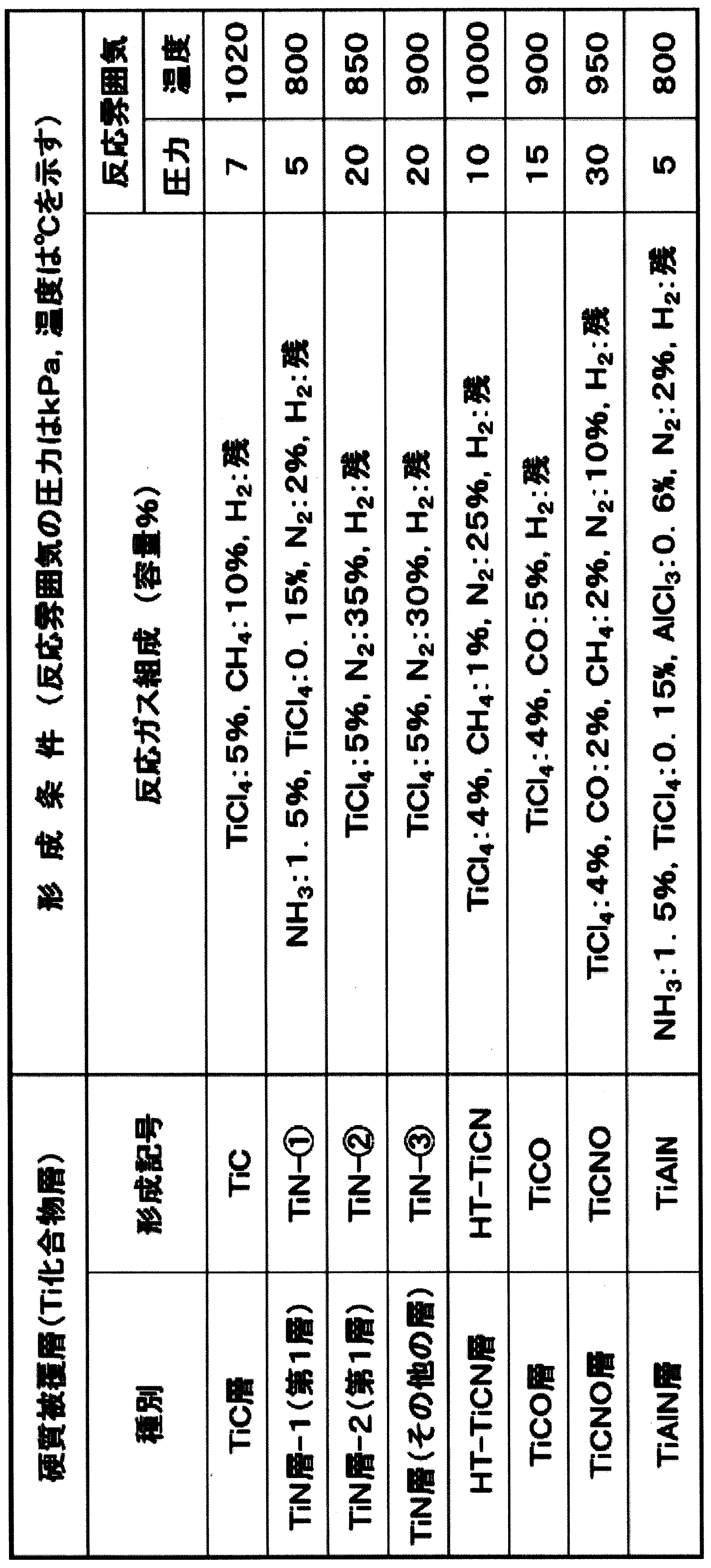
反応ガス組成(容量%):TiCl4 1~5%、CH3CN 0.5~1.5%、N2 25~40%、残部H2、
反応雰囲気温度:750~850℃、
反応雰囲気圧力:5~10kPa
反応雰囲気温度を低温にし、TiCN層の原料となるガス濃度比を低くすることで、(200)配向性の高い結晶組織が形成しやすくなり、またその組織は柱状縦長組織を有しやすくなる。
また、TiN層の形成時に、例えば、
反応ガス組成(容量%):NH3 0.5~2.0%,TiCl4 0.1~0.3%、N2 0~10%、残部H2、
反応雰囲気温度:750~850℃、
反応雰囲気圧力:5~8kPa
のような条件で作成することで、アスペクト比が5以上である柱状縦長組織を有する結晶粒を形成しやすくなる。
この発明における下部層のTi化合物層は、例えば、以下のようにして形成する。即ち、通常の化学蒸着装置を使用して、TiC層、TiN層、TiCN層、TiCO層、TiCNO層およびTiAlN層のうちの1層または2層以上からなる種々のTi化合物層を蒸着形成する。
その中で、(200)配向性の高いTiCN層、あるいは、アスペクト比が5以上である柱状縦長組織を有する結晶粒が、Ti化合物層の縦断面の70面積%以上を占めるTiCN層は、例えば、以下の蒸着方法によって形成することができる。
反応ガス組成(容量%):TiCl4 1~5%、CH3CN 0.5~1.5%、N2 25~40%、残部H2、
反応雰囲気温度:750~850℃、
反応雰囲気圧力:5~10kPa
反応雰囲気温度を低温にし、TiCN層の原料となるガス濃度比を低くすることで、(200)配向性の高い結晶組織が形成しやすくなり、またその組織は柱状縦長組織を有しやすくなる。
また、TiN層の形成時に、例えば、
反応ガス組成(容量%):NH3 0.5~2.0%,TiCl4 0.1~0.3%、N2 0~10%、残部H2、
反応雰囲気温度:750~850℃、
反応雰囲気圧力:5~8kPa
のような条件で作成することで、アスペクト比が5以上である柱状縦長組織を有する結晶粒を形成しやすくなる。
本願発明の被覆工具によれば、工具基体の表面に形成されたTi化合物層を含む硬質被覆層は、Ti化合物層として少なくとも1層のTiCN層を含み、かつ、該TiCN層の内の少なくとも1つの層は、(200)面にX線回折による最大回折ピーク強度が現れ、かつ、配向性指数Tc(200)は2.0以上である(200)配向性を有するため、すぐれた耐塑性変形性を備える。
その結果、TiCN層表面への大きなせん断力が作用する高負荷・低速切削加工条件で使用した場合でも、本願発明の被覆工具は、TiCN層の備えるすぐれた耐塑性変形性によって、結晶粒の脱落、チッピング・欠損・剥離等の異常損傷の発生を抑制することができ、長期の使用にわたってすぐれた耐摩耗性を発揮するのである。
さらに、Ti化合物層において、アスペクト比が5以上である柱状縦長組織を有する結晶粒の面積割合が、下部層の縦断面の70面積%以上であることによって、耐摩耗性をより向上させることができ、切削工具の長寿命化を図ることができる。
その結果、TiCN層表面への大きなせん断力が作用する高負荷・低速切削加工条件で使用した場合でも、本願発明の被覆工具は、TiCN層の備えるすぐれた耐塑性変形性によって、結晶粒の脱落、チッピング・欠損・剥離等の異常損傷の発生を抑制することができ、長期の使用にわたってすぐれた耐摩耗性を発揮するのである。
さらに、Ti化合物層において、アスペクト比が5以上である柱状縦長組織を有する結晶粒の面積割合が、下部層の縦断面の70面積%以上であることによって、耐摩耗性をより向上させることができ、切削工具の長寿命化を図ることができる。
本願発明の被覆工具の実施形態について、実施例に基づいて具体的に説明する。
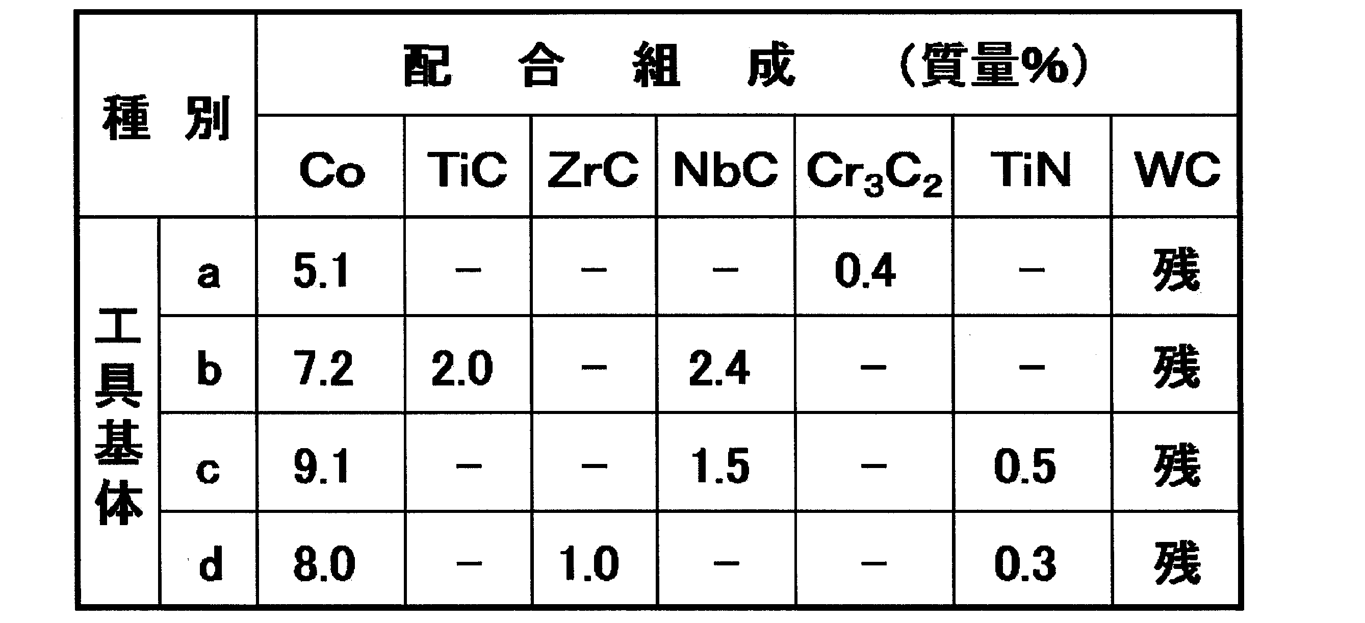
原料粉末として、いずれも1~3μmの平均粒径を有するWC粉末、TiC粉末、ZrC粉末、NbC粉末、Cr3C2粉末、TiN粉末、およびCo粉末を用意し、これら原料粉末を、表1に示される配合組成に配合し、さらにワックスを加えてアセトン中で24時間ボールミル混合し、減圧乾燥した後、98MPaの圧力で所定形状の圧粉体にプレス成形し、この圧粉体を5Paの真空中、1370~1470℃の範囲内の所定の温度に1時間保持の条件で真空焼結し、焼結後、ISO規格CNMG120408のインサート形状をもったWC基超硬合金製の工具基体a~dをそれぞれ製造した。
また、原料粉末として、いずれも0.5~2μmの平均粒径を有するTiCN(質量比でTiC/TiN=50/50)粉末、ZrC粉末、TaC粉末、Mo2C粉末、WC粉末、Co粉末およびNi粉末を用意し、これら原料粉末を、表2に示される配合組成に配合し、ボールミルで24時間湿式混合し、乾燥した後、98MPaの圧力で圧粉体にプレス成形し、この圧粉体を1.3kPaの窒素雰囲気中、温度:1500℃に1時間保持の条件で焼結し、焼結後、ISO規格CNMG120412のインサート形状をもったTiCN基サーメット製の工具基体eを作製した。
ついで、これらの工具基体a~dおよび工具基体eのそれぞれを、通常の化学蒸着装置に装入し、表3、表4に示される条件で、表6に示される目標層厚のTi化合物層を蒸着形成することにより、表6に示される本発明被覆工具1~13をそれぞれ製造した。
なお、表3で示すHT-TiCN層は、段落0016で示したTiCN層よりも反応雰囲気温度が高温で作製したTiCN層を示す。
また、表3において、アスペクト比が5以上である柱状縦長組織の結晶粒が形成されやすいTi化合物層の成膜条件は、TiN層-1(第1層)とTiAlN層である。
なお、表3で示すHT-TiCN層は、段落0016で示したTiCN層よりも反応雰囲気温度が高温で作製したTiCN層を示す。
また、表3において、アスペクト比が5以上である柱状縦長組織の結晶粒が形成されやすいTi化合物層の成膜条件は、TiN層-1(第1層)とTiAlN層である。
また、比較の目的で、工具基体a~dおよび工具基体eのそれぞれを、通常の化学蒸着装置に装入し、表3、表5に示される条件で、表7に示される目標層厚のTi化合物層を蒸着形成することにより、表7に示される比較例被覆工具1~13をそれぞれ製造した。
本発明被覆工具1~13および比較被覆工具1~13のTi化合物層のTiCN層について、X線回折により、各格子面からの回折ピーク強度を測定した。
図1に、本発明被覆工具1について求めたチャートを示す。
なお、X線回折は、装置としてスペクトリス社PANalytical Empyreanを用い、CuKα線による2θ‐θ法で測定した。
測定条件は、測定範囲(2θ):30~130度、X線出力:45kV、40mA、発散スリット:0.5度、スキャンステップ:0.013度、1ステップ辺り測定時間:0.48sec/stepである。
上記で求めたチャートから、(200)面からの回折ピーク強度が、他の格子面からの回折ピーク強度に対して最大であるか否かを判定した。
表6、表7に、その判定結果を示す。
図1に、本発明被覆工具1について求めたチャートを示す。
なお、X線回折は、装置としてスペクトリス社PANalytical Empyreanを用い、CuKα線による2θ‐θ法で測定した。
測定条件は、測定範囲(2θ):30~130度、X線出力:45kV、40mA、発散スリット:0.5度、スキャンステップ:0.013度、1ステップ辺り測定時間:0.48sec/stepである。
上記で求めたチャートから、(200)面からの回折ピーク強度が、他の格子面からの回折ピーク強度に対して最大であるか否かを判定した。
表6、表7に、その判定結果を示す。
また、上記回折ピーク強度の測定結果に基づき、配向性指数Tc(200)を求めた。
配向性指数Tc(200)は、下記式によって算出した。
配向性指数Tc(200)は、下記式によって算出した。
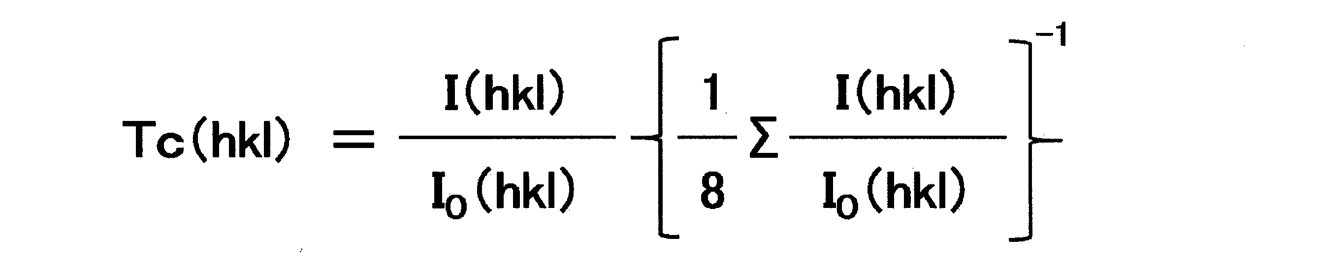
ここで、I(hkl)は測定された(hkl)面の回折ピーク強度を示し、I0(hkl)はJCPDSカード(Joint Committee on Powder Diffraction Standards(粉末X線回折標準))で表される(hkl)面を構成するTiCとTiNの粉末回折強度の平均値を示す。また、(hkl)は、(111)、(200)、(220)、(311)、(222)、(331)、(420)、(422)の8面である。
表6、表7に、上記で算出した配向性指数Tc(200)の値を示す。
表6、表7に、上記で算出した配向性指数Tc(200)の値を示す。
また、本発明被覆工具1~13および比較被覆工具1~13の下部層のTiCN層の縦断面について、走査型電子顕微鏡(倍率5000倍)を用いて、工具基体と平行な方向に10μm、工具基体と垂直な方向にTiCN層の層厚分の高さの領域内に存在するTiCN結晶粒のそれぞれについて最大粒子幅W、最大粒子長さLを測定するとともに、アスペクト比L/Wの値を求め、アスペクト比L/Wが5以上である結晶粒が、TiCN層の縦断面に占める面積割合を求めた。
表6、表7に、上記で求めた面積割合を示す。
表6、表7に、上記で求めた面積割合を示す。
また、本発明被覆工具1~13、比較例被覆工具1~13の硬質被覆層の各構成層の厚さを、走査型電子顕微鏡を用いて測定(縦断面測定)したところ、いずれも目標層厚と実質的に同じ平均層厚(5点測定の平均値)を示した。




つぎに、本発明被覆工具1~13、比較例被覆工具1~13の各種の被覆工具について、いずれも工具鋼製バイトの先端部に固定治具にてネジ止めした状態で、次の切削条件A、切削条件Bで切削試験を実施した。
≪切削条件A≫
被削材:SUS630,
切削速度:120m/min,
切り込み:3.0mm
送り:0.3mm/rev.
切削時間:5分間
の条件でのステンレス鋼丸棒の乾式連続高切り込み切削試験。
≪切削条件B≫
被削材:SUS304,
切削速度:200m/min,
切り込み:2.0mm
送り:0.3mm/rev,
切削時間:5分間
の条件でのステンレス鋼4本スリット材の乾式断続切削試験。
上記の切削試験における切れ刃の逃げ面摩耗幅を測定するとともに、チッピング、欠損、剥離等の異常損傷の発生状況を肉眼で観察した。
表8、表9に、この試験結果を示す。
≪切削条件A≫
被削材:SUS630,
切削速度:120m/min,
切り込み:3.0mm
送り:0.3mm/rev.
切削時間:5分間
の条件でのステンレス鋼丸棒の乾式連続高切り込み切削試験。
≪切削条件B≫
被削材:SUS304,
切削速度:200m/min,
切り込み:2.0mm
送り:0.3mm/rev,
切削時間:5分間
の条件でのステンレス鋼4本スリット材の乾式断続切削試験。
上記の切削試験における切れ刃の逃げ面摩耗幅を測定するとともに、チッピング、欠損、剥離等の異常損傷の発生状況を肉眼で観察した。
表8、表9に、この試験結果を示す。
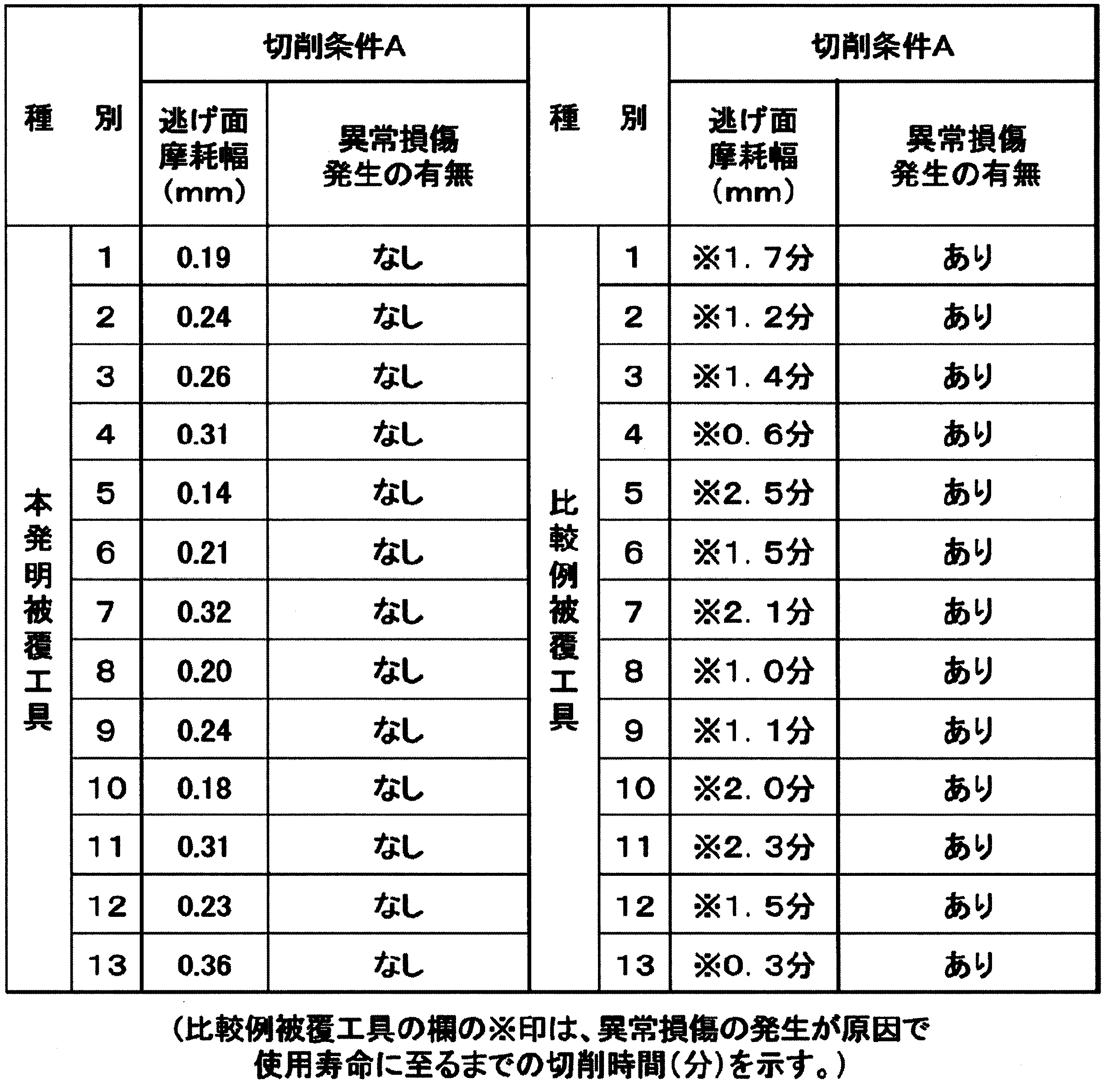
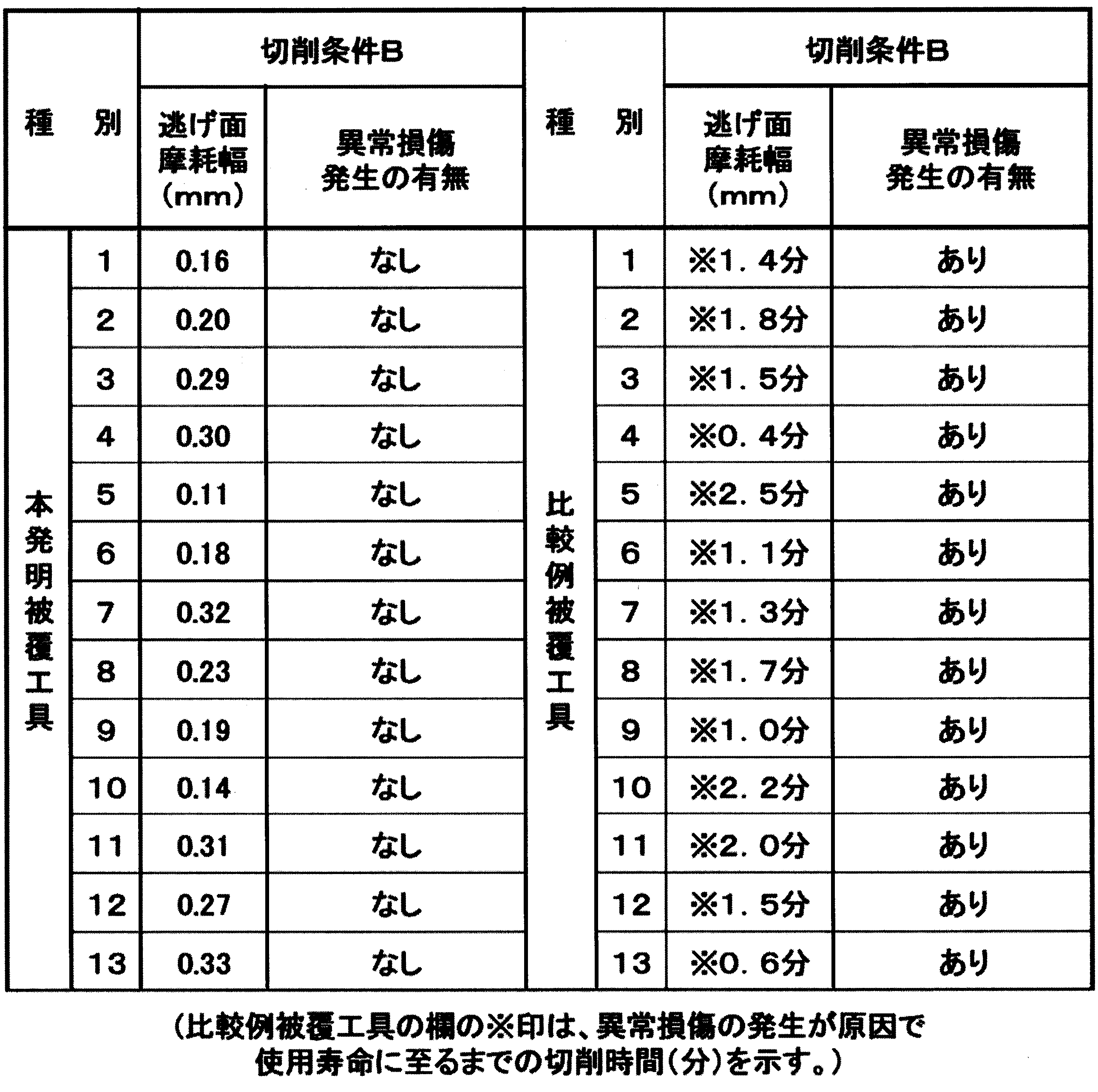
表8、表9に示される結果から、本発明被覆工具1~13は、硬質被覆層のTi化合物層として、耐塑性変形性にすぐれるTiCN層が存在するため、TiCN結晶粒の脱落、これを原因とするチッピング、欠損、剥離の発生もなく、すぐれた耐摩耗性を発揮する。
これに対して、比較例被覆工具1~13は、高負荷・低速切削加工においては、TiCN結晶粒の脱落、チッピング・欠損・剥離等の異常損傷の発生により、比較的短時間で使用寿命に至ることが明らかである。
これに対して、比較例被覆工具1~13は、高負荷・低速切削加工においては、TiCN結晶粒の脱落、チッピング・欠損・剥離等の異常損傷の発生により、比較的短時間で使用寿命に至ることが明らかである。
前述のように、本願発明の被覆工具は、切れ刃に高負荷(大きなせん断力)が作用する高負荷・低速切削において特にすぐれた切削性能を発揮するが、各種鋼や鋳鉄などの通常の条件での連続切削や断続切削にも勿論用いることができる。
Claims (3)
- 炭化タングステン基超硬合金または炭窒化チタン基サーメットで構成された工具基体の表面に、硬質被覆層が形成されている表面被覆切削工具において、
(a)前記硬質被覆層は、Tiの炭化物層、窒化物層、炭窒化物層、炭酸化物層および炭窒酸化物層から選ばれる1層または2層以上からなり、その内の少なくとも1層はTiの炭窒化物層で構成された2~15μmの合計平均層厚を有するTi化合物層を含み、
(b)前記Ti化合物層中の少なくとも1層のTiの炭窒化物層は、(200)面にX線回折による最大回折ピーク強度が現れ、かつ、配向性指数Tc(200)は2.0以上であることを特徴とする表面被覆切削工具。 - 前記Ti化合物層の縦断面において、アスペクト比が5以上である柱状縦長組織を有する結晶粒が占める面積割合は、70面積%以上であることを特徴とする請求項1に記載の表面被覆切削工具。
- 前記Ti化合物層において、すべてのTiの炭窒化物層の層厚が4~13μmであることを特徴とする請求項1または2に記載の表面被覆切削工具。
Applications Claiming Priority (4)
| Application Number | Priority Date | Filing Date | Title |
|---|---|---|---|
| JP2016027726 | 2016-02-17 | ||
| JP2016-027726 | 2016-02-17 | ||
| JP2017-026574 | 2017-02-16 | ||
| JP2017026574A JP6853449B2 (ja) | 2016-02-17 | 2017-02-16 | 表面被覆切削工具 |
Publications (1)
| Publication Number | Publication Date |
|---|---|
| WO2017142058A1 true WO2017142058A1 (ja) | 2017-08-24 |
Family
ID=59626003
Family Applications (1)
| Application Number | Title | Priority Date | Filing Date |
|---|---|---|---|
| PCT/JP2017/005848 Ceased WO2017142058A1 (ja) | 2016-02-17 | 2017-02-17 | 表面被覆切削工具 |
Country Status (1)
| Country | Link |
|---|---|
| WO (1) | WO2017142058A1 (ja) |
Citations (5)
| Publication number | Priority date | Publication date | Assignee | Title |
|---|---|---|---|---|
| JPH0847999A (ja) * | 1994-03-22 | 1996-02-20 | Sandvik Ab | 被覆超硬質焼結合金物品とその製造方法 |
| WO2012144088A1 (ja) * | 2011-04-21 | 2012-10-26 | 住友電工ハードメタル株式会社 | 表面被覆切削工具およびその製造方法 |
| WO2014142190A1 (ja) * | 2013-03-12 | 2014-09-18 | 日立ツール株式会社 | 硬質皮膜、硬質皮膜被覆部材、及びそれらの製造方法 |
| WO2014198881A1 (en) * | 2013-06-14 | 2014-12-18 | Sandvik Intellectual Property Ab | Coated cutting tool |
| JP2015500148A (ja) * | 2011-12-14 | 2015-01-05 | サンドビック インテレクチュアル プロパティー アクティエボラーグ | 被覆切削工具及びその製造方法 |
-
2017
- 2017-02-17 WO PCT/JP2017/005848 patent/WO2017142058A1/ja not_active Ceased
Patent Citations (5)
| Publication number | Priority date | Publication date | Assignee | Title |
|---|---|---|---|---|
| JPH0847999A (ja) * | 1994-03-22 | 1996-02-20 | Sandvik Ab | 被覆超硬質焼結合金物品とその製造方法 |
| WO2012144088A1 (ja) * | 2011-04-21 | 2012-10-26 | 住友電工ハードメタル株式会社 | 表面被覆切削工具およびその製造方法 |
| JP2015500148A (ja) * | 2011-12-14 | 2015-01-05 | サンドビック インテレクチュアル プロパティー アクティエボラーグ | 被覆切削工具及びその製造方法 |
| WO2014142190A1 (ja) * | 2013-03-12 | 2014-09-18 | 日立ツール株式会社 | 硬質皮膜、硬質皮膜被覆部材、及びそれらの製造方法 |
| WO2014198881A1 (en) * | 2013-06-14 | 2014-12-18 | Sandvik Intellectual Property Ab | Coated cutting tool |
Similar Documents
| Publication | Publication Date | Title |
|---|---|---|
| JP5907406B2 (ja) | 硬質被覆層が高速断続切削ですぐれた耐チッピング性を発揮する表面被覆切削工具 | |
| JPWO2012063515A1 (ja) | 表面被覆切削工具 | |
| JP2013188833A (ja) | 硬質被覆層が高速断続切削ですぐれた耐チッピング性を発揮する表面被覆切削工具 | |
| JP7121234B2 (ja) | 硬質被覆層が優れた耐チッピング性を発揮する表面切削工具 | |
| WO2018042740A1 (ja) | 硬質被覆層がすぐれた耐チッピング性、耐剥離性を発揮する表面被覆切削工具 | |
| JP6853450B2 (ja) | 表面被覆切削工具 | |
| JP5402516B2 (ja) | 硬質被覆層がすぐれた耐チッピング性を発揮する表面被覆切削工具 | |
| JP2010274330A (ja) | 表面被覆切削工具 | |
| JP2004122269A (ja) | 高速重切削ですぐれた耐チッピング性を発揮する表面被覆サーメット製切削工具 | |
| JP6853449B2 (ja) | 表面被覆切削工具 | |
| JP5170828B2 (ja) | 高速断続切削加工で硬質被覆層がすぐれた耐チッピング性を発揮する表面被覆切削工具 | |
| US10076789B2 (en) | Surface-coated titanium carbonitride-based cermet cutting tool having excellent chipping resistance | |
| JP2019177424A (ja) | 硬質被覆層が優れた耐酸化性、耐溶着性を発揮する表面被覆切削工具 | |
| JP7043869B2 (ja) | 硬質被覆層がすぐれた耐溶着性と耐異常損傷性を発揮する表面被覆切削工具 | |
| JP2014184522A (ja) | 硬質被覆層がすぐれた密着性を有する表面被覆wc基超硬合金製切削工具 | |
| WO2017142058A1 (ja) | 表面被覆切削工具 | |
| WO2017142061A1 (ja) | 表面被覆切削工具 | |
| JP5569739B2 (ja) | 耐チッピング性にすぐれた表面被覆切削工具 | |
| JP5187573B2 (ja) | 高速重切削加工で硬質被覆層がすぐれた耐チッピング性と耐摩耗性を発揮する表面被覆切削工具 | |
| JP2006198740A (ja) | 硬質被覆層が高速断続切削加工ですぐれた耐チッピング性を発揮する表面被覆サーメット製切削工具 | |
| JP5686294B2 (ja) | 硬質被覆層がすぐれた耐チッピング性を発揮する表面被覆切削工具 | |
| JP5305013B2 (ja) | 硬質被覆層がすぐれた耐チッピング性、耐摩耗性を発揮する表面被覆切削工具 | |
| JP2012096303A (ja) | 耐チッピング性にすぐれた表面被覆切削工具 | |
| JP7401850B2 (ja) | 表面被覆切削工具 | |
| WO2019065683A1 (ja) | 硬質被覆層がすぐれた耐溶着性と耐異常損傷性を発揮する表面被覆切削工具 |
Legal Events
| Date | Code | Title | Description |
|---|---|---|---|
| 121 | Ep: the epo has been informed by wipo that ep was designated in this application |
Ref document number: 17753313 Country of ref document: EP Kind code of ref document: A1 |
|
| NENP | Non-entry into the national phase |
Ref country code: DE |
|
| 122 | Ep: pct application non-entry in european phase |
Ref document number: 17753313 Country of ref document: EP Kind code of ref document: A1 |