WO2017135408A1 - 高周波モジュール - Google Patents
高周波モジュール Download PDFInfo
- Publication number
- WO2017135408A1 WO2017135408A1 PCT/JP2017/003984 JP2017003984W WO2017135408A1 WO 2017135408 A1 WO2017135408 A1 WO 2017135408A1 JP 2017003984 W JP2017003984 W JP 2017003984W WO 2017135408 A1 WO2017135408 A1 WO 2017135408A1
- Authority
- WO
- WIPO (PCT)
- Prior art keywords
- terminal
- frequency module
- common terminal
- matching circuit
- band
- Prior art date
- Legal status (The legal status is an assumption and is not a legal conclusion. Google has not performed a legal analysis and makes no representation as to the accuracy of the status listed.)
- Ceased
Links
Images




Classifications
-
- H—ELECTRICITY
- H01—ELECTRIC ELEMENTS
- H01Q—ANTENNAS, i.e. RADIO AERIALS
- H01Q23/00—Antennas with active circuits or circuit elements integrated within them or attached to them
-
- H—ELECTRICITY
- H04—ELECTRIC COMMUNICATION TECHNIQUE
- H04B—TRANSMISSION
- H04B1/00—Details of transmission systems, not covered by a single one of groups H04B3/00 - H04B13/00; Details of transmission systems not characterised by the medium used for transmission
- H04B1/02—Transmitters
- H04B1/04—Circuits
- H04B1/0458—Arrangements for matching and coupling between power amplifier and antenna or between amplifying stages
-
- H—ELECTRICITY
- H03—ELECTRONIC CIRCUITRY
- H03H—IMPEDANCE NETWORKS, e.g. RESONANT CIRCUITS; RESONATORS
- H03H7/00—Multiple-port networks comprising only passive electrical elements as network components
- H03H7/01—Frequency selective two-port networks
-
- H—ELECTRICITY
- H03—ELECTRONIC CIRCUITRY
- H03H—IMPEDANCE NETWORKS, e.g. RESONANT CIRCUITS; RESONATORS
- H03H7/00—Multiple-port networks comprising only passive electrical elements as network components
- H03H7/01—Frequency selective two-port networks
- H03H7/0115—Frequency selective two-port networks comprising only inductors and capacitors
-
- H—ELECTRICITY
- H04—ELECTRIC COMMUNICATION TECHNIQUE
- H04B—TRANSMISSION
- H04B1/00—Details of transmission systems, not covered by a single one of groups H04B3/00 - H04B13/00; Details of transmission systems not characterised by the medium used for transmission
- H04B1/06—Receivers
- H04B1/16—Circuits
- H04B1/18—Input circuits, e.g. for coupling to an antenna or a transmission line
-
- H—ELECTRICITY
- H04—ELECTRIC COMMUNICATION TECHNIQUE
- H04B—TRANSMISSION
- H04B1/00—Details of transmission systems, not covered by a single one of groups H04B3/00 - H04B13/00; Details of transmission systems not characterised by the medium used for transmission
- H04B1/38—Transceivers, i.e. devices in which transmitter and receiver form a structural unit and in which at least one part is used for functions of transmitting and receiving
- H04B1/40—Circuits
-
- H—ELECTRICITY
- H04—ELECTRIC COMMUNICATION TECHNIQUE
- H04B—TRANSMISSION
- H04B1/00—Details of transmission systems, not covered by a single one of groups H04B3/00 - H04B13/00; Details of transmission systems not characterised by the medium used for transmission
- H04B1/38—Transceivers, i.e. devices in which transmitter and receiver form a structural unit and in which at least one part is used for functions of transmitting and receiving
- H04B1/40—Circuits
- H04B1/50—Circuits using different frequencies for the two directions of communication
- H04B1/52—Hybrid arrangements, i.e. arrangements for transition from single-path two-direction transmission to single-direction transmission on each of two paths or vice versa
- H04B1/525—Hybrid arrangements, i.e. arrangements for transition from single-path two-direction transmission to single-direction transmission on each of two paths or vice versa with means for reducing leakage of transmitter signal into the receiver
-
- H—ELECTRICITY
- H10—SEMICONDUCTOR DEVICES; ELECTRIC SOLID-STATE DEVICES NOT OTHERWISE PROVIDED FOR
- H10W—GENERIC PACKAGES, INTERCONNECTIONS, CONNECTORS OR OTHER CONSTRUCTIONAL DETAILS OF DEVICES COVERED BY CLASS H10
- H10W44/00—Electrical arrangements for controlling or matching impedance
- H10W44/20—Electrical arrangements for controlling or matching impedance at high-frequency [HF] or radio frequency [RF]
-
- H—ELECTRICITY
- H01—ELECTRIC ELEMENTS
- H01Q—ANTENNAS, i.e. RADIO AERIALS
- H01Q5/00—Arrangements for simultaneous operation of antennas on two or more different wavebands, e.g. dual-band or multi-band arrangements
- H01Q5/50—Feeding or matching arrangements for broad-band or multi-band operation
-
- H—ELECTRICITY
- H03—ELECTRONIC CIRCUITRY
- H03H—IMPEDANCE NETWORKS, e.g. RESONANT CIRCUITS; RESONATORS
- H03H7/00—Multiple-port networks comprising only passive electrical elements as network components
- H03H7/38—Impedance-matching networks
-
- H—ELECTRICITY
- H04—ELECTRIC COMMUNICATION TECHNIQUE
- H04B—TRANSMISSION
- H04B1/00—Details of transmission systems, not covered by a single one of groups H04B3/00 - H04B13/00; Details of transmission systems not characterised by the medium used for transmission
-
- H—ELECTRICITY
- H10—SEMICONDUCTOR DEVICES; ELECTRIC SOLID-STATE DEVICES NOT OTHERWISE PROVIDED FOR
- H10W—GENERIC PACKAGES, INTERCONNECTIONS, CONNECTORS OR OTHER CONSTRUCTIONAL DETAILS OF DEVICES COVERED BY CLASS H10
- H10W44/00—Electrical arrangements for controlling or matching impedance
- H10W44/20—Electrical arrangements for controlling or matching impedance at high-frequency [HF] or radio frequency [RF]
- H10W44/241—Electrical arrangements for controlling or matching impedance at high-frequency [HF] or radio frequency [RF] for passive devices or passive elements
- H10W44/248—Electrical arrangements for controlling or matching impedance at high-frequency [HF] or radio frequency [RF] for passive devices or passive elements for antennas
Definitions
- the present invention relates to a high frequency module.
- a switch circuit including a common terminal connected to an antenna and a plurality of selection terminals connected to a transmission system circuit or a reception system circuit is provided (for example, see Patent Document 1).
- the phase of the transmission signal is adjusted by providing the phase circuit in the transmission path connected to the selected terminal (selection terminal) of the switch IC (switch circuit). Therefore, the isolation between the transmission path provided with the phase circuit and the transmission path connected to another selected terminal is enhanced.
- the number of selection terminals provided in one switch circuit tends to increase. For this reason, when the number of selection terminals is increased while suppressing an increase in the size of the switch circuit, there is a possibility that the isolation between the selection terminals may be deteriorated due to a decrease in the interval between the selection terminals.
- isolation indicates the degree of separation between any two points, and will be described below as the degree of separation between the selected terminals.
- an object of the present invention is to provide a high-frequency module capable of enhancing isolation while suppressing deterioration of pass characteristics.
- a high-frequency module includes a first common terminal, a second common terminal, and a plurality of selection terminals, the first common terminal and the second common terminal. Are selectively connected to different selection terminals among the plurality of selection terminals, and a matching circuit is connected to the second common terminal without being connected to the antenna.
- the matching circuit connected to the second common terminal of the first switch circuit, unnecessary signals leaking from the selection terminal connected to the first common terminal can be transmitted from the other selection terminals to the first. It becomes difficult to leak out of the switch circuit. Specifically, an unnecessary signal leaked (around) to a selection terminal connected to the second common terminal is more likely to leak from the second common terminal connected to the matching circuit than the selection terminal. As a result, an unnecessary signal leaking out of the first switch circuit from the selection terminal can be suppressed, so that isolation can be enhanced. Also, the matching circuit is not connected to any one or more antennas. In other words, the matching circuit is provided in a path different from the signal path to be transmitted by the high-frequency module, so that it is difficult for the pass characteristics to deteriorate. As described above, the high-frequency module according to this aspect can increase the isolation while suppressing the deterioration of the passage characteristics.
- the matching circuit may be connected in series with the second common terminal.
- the matching circuit may include a shunt connection type element provided between the second common terminal and a ground potential.
- the matching circuit has the shunt connection type element as described above, an unnecessary signal that has entered the selection terminal connected to the second common terminal can easily flow to the ground via the second common terminal and the matching circuit. . For this reason, since an unnecessary signal leaking out of the first switch circuit from the selection terminal can be suppressed, the isolation can be further enhanced.
- the matching circuit may be a filter type matching circuit including a frequency band corresponding to a selection terminal connected to the first common terminal among the plurality of selection terminals in a pass band.
- the matching circuit is a filter-type matching circuit, it is possible to suppress reflection of unnecessary signals leaking from the second common terminal to the matching circuit. Therefore, an unnecessary signal leaking out of the first switch circuit from the selection terminal connected to the second common terminal due to such reflection can be suppressed. Therefore, the isolation can be further increased.
- the matching circuit may be a low-pass filter type matching circuit.
- the matching circuit is a low-pass filter type matching circuit, a high-frequency module can be easily manufactured even when a wide pass band is required for the matching circuit.
- a first antenna connected to the first common terminal may be provided.
- the first antenna By providing the first antenna in this way, it is possible to realize a high-frequency module with a built-in antenna that can improve isolation while suppressing deterioration of pass characteristics.
- a high-frequency module includes a first common terminal, a second common terminal, and a plurality of selection terminals.
- a first switch circuit that selectively connects a second common terminal to different selection terminals of the plurality of selection terminals; a second switch circuit that includes an input terminal, a first output terminal, and a second output terminal;
- the second common terminal is connected to the input terminal, and the second switch circuit selectively connects the input terminal to the first output terminal and the second output terminal.
- the matching circuit is connected to the second output terminal.
- the second switch circuit that selectively connects the second common terminal to the second antenna and the matching circuit in this way, transmission and reception are performed using both the first antenna and the second antenna, for example, carrier aggregation (CA : Carrier Aggregation) method. Specifically, it is possible to increase isolation while suppressing deterioration of the pass characteristic during non-CA operation, and to enable a CA operation with good pass characteristics.
- CA Carrier Aggregation
- a second antenna connected to the first output terminal may be provided.
- a high-frequency module capable of enhancing isolation while suppressing deterioration of pass characteristics is provided.
- FIG. 1 is a circuit diagram of the high-frequency module according to the first embodiment.
- FIG. 2 is a graph showing the isolation characteristics of the high-frequency module according to the first embodiment.
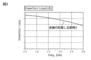
- FIG. 3 is a graph showing pass characteristics of the high-frequency module according to the first embodiment.
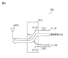
- FIG. 4 is a circuit diagram of the high-frequency module according to Comparative Example 1 and a diagram illustrating the problem.
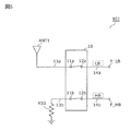
- FIG. 5 is a circuit diagram showing a configuration of a high-frequency module according to Comparative Example 2.
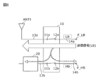
- FIG. 6 is a diagram schematically illustrating a state in which a signal of the high-frequency module according to Embodiment 1 is propagated.
- FIG. 7 is a circuit diagram of the high-frequency module according to the second embodiment.
- FIG. 1 is a circuit diagram of the high-frequency module according to the first embodiment.
- FIG. 2 is a graph showing the isolation characteristics of the high-frequency module according to the first embodiment.
- FIG. 3 is a graph showing pass characteristics of the high-frequency module according to
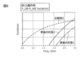
- FIG. 8 is a graph showing the isolation characteristics of the high-frequency module according to Embodiment 2 during non-CA operation.
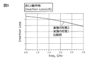
- FIG. 9 is a graph showing pass characteristics when the high-frequency module according to Embodiment 2 is in non-CA operation.
- FIG. 10 is a graph showing pass characteristics related to the first antenna and the second antenna during the CA operation of the high-frequency module according to the second embodiment.
- FIG. 11 is a circuit diagram of a high-frequency module according to a modification of the second embodiment.
- FIG. 1 is a circuit diagram of a high-frequency module 1 according to Embodiment 1 of the present invention.
- the high-frequency module 1 shown in the figure is a multi-band compatible high-frequency module, and is disposed, for example, at the front end of a communication device such as a mobile phone.
- the high frequency module 1 is connected to the first antenna ANT1, and incorporates the first antenna ANT1 in the present embodiment. Note that the high-frequency module 1 may not include the first antenna ANT1.
- the high frequency module 1 includes a first antenna ANT1 for a high frequency signal (transmission signal or reception signal) of a predetermined band among a plurality of bands, and a signal processing circuit (non-frequency integrated circuit) such as RFIC (Radio Frequency Integrated Circuit) that processes the high frequency signal. (Transmission)
- a signal processing circuit non-frequency integrated circuit
- RFIC Radio Frequency Integrated Circuit
- the high frequency module 1 includes an LB band terminal P_LB to which a low frequency (Low Band, LB band) high frequency signal is input or output, and a high frequency (High Band, HB band). And an HB band terminal P_HB to which a signal is input or output.
- the high frequency module 1 selectively transmits a high frequency signal between the first antenna ANT1 and the LB band terminal P_LB and between the first antenna ANT1 and the HB band terminal P_HB.
- the high frequency module 1 corresponds to LTE (Long Term Evolution) and transmits a high frequency signal of a Band (frequency band) defined by 3GPP (Third Generation Partnership Project).
- the high frequency module 1 transmits, for example, a Band 8 (transmission band: 880 to 915 MHz, reception band: 925 to 960 MHz) high frequency signal as an LB band high frequency signal, and a Band 1 (transmission band: 1920 to 1980 MHz) as an HB band high frequency signal.
- Reception band 2110-2170 MHz).
- the high-frequency module 1 includes a first switch circuit 10 and a matching circuit 20 as shown in FIG.
- the first switch circuit 10 includes a first common terminal 11a connected to the first antenna ANT1, a second common terminal 11b not connected to the first antenna ANT1, and a plurality of selection terminals (here, two selection terminals 12a and 12b). ).
- the first switch circuit 10 selectively connects the first common terminal 11a and the second common terminal 11b to different selection terminals of the plurality of selection terminals 12a and 12b, for example, based on an external control signal. To do. That is, the first common terminal 11a and the second common terminal 11b are exclusively connected to the plurality of selection terminals 12a and 12b.
- the first common terminal 11a is a common terminal that is connected to the first antenna ANT1 through the transmission path 13a and not connected to the matching circuit 20, and is connected to one of the selection terminals 12a and 12b based on, for example, a control signal.
- the first common terminal 11a may be connected to the first antenna ANT1 via a matching circuit or filter for the first antenna ANT1, which is different from the matching circuit 20.
- the second common terminal 11b is connected to the matching circuit 20 via the transmission path 13b and is not connected to the first antenna ANT1, and is connected to the other of the selection terminals 12a and 12b based on, for example, a control signal.
- the second common terminal 11b may be connected to an antenna different from the first antenna ANT1. That is, the high frequency module 1 may be connected to a plurality of antennas including the first antenna ANT1.
- the selection terminals 12a and 12b correspond to different bands
- the selection terminal 12a corresponds to the LB band (for example, Band8)
- the selection terminal 12b corresponds to the HB band (for example, Band1).
- the selection terminal 12a is connected to the LB band terminal P_LB via the transmission path 14a.
- the selection terminal 12b is connected to the HB band terminal P_HB via the transmission path 14b.
- the bands corresponding to each of the selection terminals 12a and 12b are not limited to this.
- the selection terminal 12a may correspond to the HB band and the selection terminal 12b may correspond to the LB band.
- the selection terminals 12a and 12b may correspond to the same band.
- the first switch circuit 10 is configured by a high-frequency switch IC (Integrated Circuit) of DPDT (Double Pole Double Throw), and is configured by, for example, one chip.
- the various terminals of the first switch circuit 10 are, for example, surface electrodes provided on an IC chip constituting the first switch circuit 10. (Pad) or a wiring pattern connected to the surface electrode.
- the matching circuit 20 is connected to the second common terminal 11b without being connected to any one or more antennas including the first antenna ANT1. That is, in the present embodiment, the matching circuit 20 is connected to the second common terminal 11b without being connected to the first antenna ANT1. That is, since the matching circuit 20 is not connected to any antenna, it is different from a so-called antenna matching circuit.
- the matching circuit 20 is a filter type matching circuit including a frequency band corresponding to a selection terminal connected to the first common terminal 11a among the plurality of selection terminals 12a and 12b in the pass band.
- the matching circuit 20 since the first common terminal 11a can be connected to any of the plurality of selection terminals 12a and 12b, the matching circuit 20 includes both the LB band and the HB band in the pass band.
- the matching circuit 20 is a low-pass filter type matching circuit.
- the matching circuit 20 includes a shunt connection type element (capacitor 212 in this case) provided between the second common terminal 11b and the ground potential.
- the matching circuit 20 includes an inductor 211 having one end connected to the second common terminal 11b and a capacitor 212 having one end connected to the other end of the inductor 211 and the other end connected to the ground potential.
- the matching circuit 20 includes the inductor 211 connected in series to the transmission path 13b and the capacitor 212 shunt-connected between the transmission path 13b and the ground potential.
- the constants of the inductor 211 and the capacitor 212 are not particularly limited, and are determined as appropriate so that the pass band of the low-pass filter constituted by these includes the frequency band corresponding to the selection terminal connected to the first common terminal 11a described above. Is done.
- the circuit configuration of the matching circuit 20 is not limited to this, and, for example, an inductor connected in series to the transmission path 13b and a capacitor connected in shunt may be connected in multiple stages.
- Such a matching circuit 20 is, for example, a piezoelectric chip constituted by a surface acoustic wave filter using a surface acoustic wave (SAW). Note that the matching circuit 20 is not limited to an elastic wave filter using SAW, and may be an elastic wave filter using a bulk wave (BAW: Bulk Acoustic Wave). Further, a filter configured by appropriately combining a chip inductor and a chip capacitor may be used.
- SAW surface acoustic wave
- the side opposite to the second common terminal 11b (the left side in the figure) of the matching circuit 20 is connected to the ground potential. That is, the matching circuit 20 is shown as being inserted into the transmission path 13b that connects the second common terminal 11b and the ground potential, but this is not a limitation.
- another element such as an attenuator may be provided on the opposite side of the matching circuit 20 from the second common terminal 11b.
- the high frequency module 1 operates as follows. Note that the operation of the high-frequency module 1 when transmitting a high-frequency signal in the HB band is only different in the connection relationship in the first switch circuit 10 compared to the case of transmitting a high-frequency signal in the LB band. Specifically, when transmitting a high-frequency signal in the HB band, the first common terminal 11a is connected to the selection terminal 12b, and the second common terminal 11b is connected to the selection terminal 12a. Therefore, in the following, the operation of the high frequency module 1 will be described with respect to the case of transmitting an LB band high frequency signal, and the description of the case of transmitting an HB band high frequency signal will be omitted.
- the first switch circuit 10 When the high frequency module 1 transmits an LB band high frequency signal, the first switch circuit 10 operates as follows based on a control signal input from, for example, a control circuit or the like.
- the first switch circuit 10 connects the first common terminal 11a to the selection terminal 12a corresponding to the LB band, and connects the second common terminal 11b to the selection terminal 12b corresponding to the HB band.
- the high frequency signal (transmission signal) input from the LB band terminal P_LB passes through the first switch circuit 10 and is transmitted from the first antenna ANT1.
- the high frequency signal (received signal) input from the first antenna ANT1 passes through the first switch circuit 10 and is output from the LB band terminal P_LB.
- the first switch circuit 10 connects the selection terminal 12a corresponding to the transmission target signal (here, the LB band high-frequency signal) to the first common terminal 11a connected to the first antenna ANT1.
- the selection terminal 12 b corresponding to a signal that is not a transmission target (here, a high-frequency signal in the HB band) is connected to the second common terminal 11 b connected to the matching circuit 20.
- FIG. 2 and 3 are graphs showing the characteristics of the high-frequency module 1 at this time. Specifically, FIG. 2 is a graph showing the isolation characteristics of the high-frequency module 1. FIG. 3 is a graph showing pass characteristics of the high-frequency module 1.
- the pass characteristic from the LB band terminal P_LB to the HB band terminal P_HB is shown. That is, the vertical axis indicates the intensity ratio (isolation) of the signal observed at the HB band terminal P_HB with respect to the intensity of the transmission signal input from the LB band terminal P_LB.
- the horizontal axis indicates the frequency, and the frequency in the frequency band including the frequency band used (the band of the transmission signal or the band of the reception signal) of the high-frequency module 1 is shown.
- the insertion loss between the LB band terminal P_LB and the first antenna ANT1 is shown as the pass characteristic. That is, the vertical axis indicates the intensity ratio (insertion loss) of the signal observed on the input side of the first antenna ANT with respect to the intensity of the transmission signal input from the LB band terminal P_LB. The horizontal axis indicates the frequency as in FIG.
- the pass characteristic of the high frequency module 1 when transmitting the HB band high frequency signal corresponds to the pass characteristic when the HB band high frequency signal is input to the LB band terminal P_LB.
- the isolation characteristic described below also serves as a passing characteristic from the HB band terminal P_HB to the LB band terminal P_LB when transmitting an HB band high-frequency signal.
- the pass characteristic described below also serves as the pass characteristic from the HB band terminal P_HB to the first antenna ANT1 when transmitting an HB band high-frequency signal.
- FIG. 4 is a circuit diagram of the high-frequency module 801 according to the comparative example 1 and a diagram showing the problem.
- the high-frequency module 801 according to Comparative Example 1 shown in the figure does not include the matching circuit 20 as compared with the high-frequency module 1 according to the embodiment, and includes the SPDT switch circuit 810 instead of the first switch circuit 10 of DPDT.
- the common terminal 811 is connected to the selection terminal 812a corresponding to the LB band, and the selection terminal 812b corresponding to the HB band is common. It is not connected to the terminal 811.
- the high frequency module 801 when a transmission signal (unnecessary signal) leaked from the selection terminal 812a in the switch circuit 810 wraps around the selection terminal 812b, the unnecessary signal is converted into the HB band terminal P_HB. May be output from. That is, it has the isolation characteristic of the grade shown in FIG.
- Suppressing such unnecessary signals is particularly important in communication in LTE or the like from the following viewpoint. That is, when the LB band terminal P_LB or the HB band terminal P_HB is connected to a reception system circuit via a duplexer or the like, the reception system circuit is designed in accordance with a minute reception signal. For this reason, when an unnecessary signal leaks into the circuit of the receiving system, problems such as deterioration may occur in the elements constituting the circuit.
- Comparative Example 2 a configuration of Comparative Example 2 is conceivable in which a DPDT switch circuit is provided in place of the SPDT switch circuit 810, thereby eliminating the selection terminal that is opened and suppressing unnecessary signals.
- FIG. 5 is a circuit diagram showing a configuration of a high-frequency module 901 according to Comparative Example 2.
- the high-frequency module 901 shown in the figure includes the first switch circuit 10 of the DPDT like the high-frequency module 1 according to the above-described embodiment, but the second common terminal 11b replaces the matching circuit 20 with a 50 ⁇ termination resistor R50. It is different in that it is connected to the ground potential via the terminal.
- the isolation can be increased as compared with the comparative example 1. That is, even if the transmission signal leaked from the selection terminal 12a in the first switch circuit 10 wraps around the selection terminal 12b, the transmission signal passes through the second common terminal 11b connected to the selection terminal 12b. By flowing into the ground potential, it is estimated that it is difficult to output from the HB band terminal P_HB.
- FIGS 2 and 3 are graphs showing the isolation characteristics of the high-frequency module 901 according to Comparative Example 2 at this time.
- the isolation is further enhanced as compared with the high-frequency module 901 according to the comparative example 2.
- the deterioration of the pass characteristic is suppressed, and in detail, the pass characteristic is Maintained.
- “deterioration of pass characteristics” means that the insertion loss increases (deteriorates). That is, “deterioration of pass characteristics is suppressed” means that insertion loss is maintained or reduced (improved).
- the high-frequency module 1 according to the present embodiment can increase the isolation while suppressing the deterioration of the passage characteristics as compared with the comparative example 1 and the comparative example 2.
- the reason why such an effect is achieved will be described with reference to FIG.
- FIG. 6 is a diagram schematically showing how a transmission signal propagates in the high-frequency module 1 according to the present embodiment.
- the LB band transmission signal may leak from the selection terminal 12a in the first switch circuit 10 and wrap around the selection terminal 12b.
- the first switch circuit 10 when the first switch circuit 10 is formed on a semiconductor substrate, such a signal wraparound becomes prominent because the signal is likely to circulate through the semiconductor substrate.
- the first switch circuit 10 when the first switch circuit 10 is formed of an IC chip, it becomes prominent even when the distance between the selection terminal 12a and the selection terminal 12b is narrow as the IC chip is downsized.
- a selection terminal (connected to the first common terminal 11a ( In FIG. 6, an unnecessary signal leaked from the selection terminal 12a) (an LB band transmission signal in FIG. 6) is difficult to leak out of the first switch circuit 10 from another selection terminal (selection terminal 12b in FIG. 6).
- an unnecessary signal leaking (around) to the selection terminal connected to the second common terminal 11b leaks from the second common terminal 11b connected to the matching circuit 20 rather than the selection terminal. It becomes easy.
- an unnecessary signal leaking out of the first switch circuit 10 from the selection terminal can be suppressed, so that isolation can be enhanced.
- the matching circuit 20 is not connected to any one or more antennas.
- the matching circuit 20 is provided in a path (transmission path 13b in FIG. 6) different from the signal path (transmission paths 14a and 13a in FIG. 6) of the transmission target of the high-frequency module 1, and therefore it is difficult to cause deterioration of the pass characteristics.
- the high-frequency module 1 according to the present embodiment can increase the isolation while suppressing the deterioration of the pass characteristic.
- the second common terminal 11b connected to the selection terminal is connected to the matching circuit 20.
- the matching circuit 20 includes the shunt connection type element (capacitor 212 in the present embodiment), so that the selection terminal connected to the second common terminal 11b can be used.
- the unnecessary signal that has wrapped around easily flows out to the ground via the second common terminal 11 b and the matching circuit 20. For this reason, since an unnecessary signal leaking out of the first switch circuit 10 from the selection terminal can be suppressed, the isolation can be further enhanced.
- the matching circuit 20 is a filter type matching circuit, reflection of unnecessary signals leaking from the second common terminal 11b to the matching circuit 20 is suppressed. be able to. Therefore, an unnecessary signal leaking out of the first switch circuit 10 from the selection terminal connected to the second common terminal 11b due to such reflection can be suppressed. Therefore, the isolation can be further increased.
- the matching circuit 20 is a low-pass filter type matching circuit, so that the high frequency module can be used even when a wide passband is required for the matching circuit 20. Can be easily manufactured.
- the high frequency module 1 by providing the first antenna ANT1, it is possible to realize a high frequency module with a built-in antenna that can improve isolation while suppressing deterioration of pass characteristics.
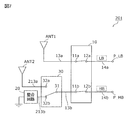
- FIG. 7 is a circuit diagram of the high-frequency module 201 according to Embodiment 2 of the present invention.
- the high-frequency module 201 shown in the figure is a high-frequency module connected to a plurality of antennas (in this embodiment, two antennas, that is, the first antenna ANT1 and the second antenna ANT2), and incorporates the plurality of antennas. Note that the high frequency module 201 may not include at least one of the plurality of antennas.
- the high frequency module 201 further includes a second switch that selectively connects the second common terminal 11b to the second antenna ANT2 and the matching circuit 20 as compared with the high frequency module 1 according to the first embodiment.
- a circuit 30 is provided.
- the second switch circuit 30 includes an input terminal 31 and two output terminals 32a and 32b.
- the input terminal 31 is selected as one of the two output terminals 32a and 32b based on a control signal from the outside. Circuit to be connected.
- Such a second switch circuit 30 is configured by, for example, a high-frequency switch IC (Integrated Circuit) of SPDT (Single Pole Double Throw), for example, in one chip.
- IC Integrated Circuit
- SPDT Single Pole Double Throw
- the input terminal 31 is connected to the matching circuit 20 via the transmission path 13b, and is connected to only one of the output terminals 32a and 32b based on, for example, a control signal.
- the output terminal 32a is a first output terminal connected to the second antenna ANT2 through the transmission path 213a.
- the output terminal 32b is a second output terminal connected to the matching circuit 20 via the transmission path 213b.
- the matching circuit 20 is connected to the second common terminal 11b without being connected to any one or more antennas (here, two antennas) to which the high-frequency module 201 is connected, as in the first embodiment.
- the matching circuit 20 is specifically connected to the output terminal 32b (second output terminal), and more specifically is connected in series with the output terminal 32b.
- the high-frequency module 201 configured as described above transmits and receives using both the first antenna ANT1 and the second antenna ANT2, compared to the high-frequency module 1 according to the first embodiment, for example, carrier aggregation A system (CA system) can be supported.
- CA system carrier aggregation A system
- the high frequency module 201 operates as follows.
- the high-frequency module 201 operates using only one frequency band among a plurality of frequency bands (during non-CA operation) will be described.
- the first switch circuit 10 When the high frequency module 201 transmits an LB band high frequency signal, the first switch circuit 10 operates in the same manner as in the first embodiment. That is, the first switch circuit 10 connects the first common terminal 11a to the selection terminal 12a corresponding to the LB band, and connects the second common terminal 11b to the selection terminal 12b corresponding to the HB band.
- the second switch circuit 30 connects the input terminal 31 to the output terminal 32b.
- FIGS. 8 and 9 are graphs showing the characteristics of the high-frequency module 201 at this time. Specifically, FIG. 8 is a graph showing the isolation characteristics of the high-frequency module 201 during non-CA operation. FIG. 9 is a graph showing pass characteristics when the high-frequency module 201 is in a non-CA operation. In these figures, for reference, the isolation characteristics and pass characteristics of the first embodiment and the comparative example 2 shown in FIGS. 2 and 3 are also shown.
- the isolation is ensured to the same extent as the high frequency module 1 according to the first embodiment. That is, according to the high frequency module 201 according to the present embodiment, the isolation is further enhanced as compared with the high frequency module 901 according to the comparative example 2.
- the pass characteristics are maintained to the same extent as the high frequency module 1 according to the first embodiment. That is, according to the high frequency module 201 according to the present embodiment, compared with the high frequency module 901 according to the comparative example 2, the deterioration of the pass characteristics is suppressed, and in detail, the pass characteristics are maintained.
- the high frequency module 201 when transmitting a LB band high frequency signal, connects the first antenna ANT1, the matching circuit 20, the LB band terminal P_LB, and the HB band terminal P_HB by the operation as described above.
- the relationship is the same as that of the high-frequency module 1 according to the first embodiment. For this reason, the high frequency module 201 at the time of non-CA operation
- the high frequency module 201 operates using two or more frequency bands among a plurality of frequency bands (during CA operation) will be described.
- the first switch circuit 10 When the high frequency module 201 transmits high frequency signals in both the LB band and the HB band, the first switch circuit 10 operates in the same manner as in the first embodiment. That is, the first switch circuit 10 connects the first common terminal 11a to the selection terminal 12a corresponding to the LB band, and connects the second common terminal 11b to the selection terminal 12b corresponding to the HB band.
- the connection relationship of the first switch circuit 10 is not limited to this.
- the first common terminal 11a is connected to the selection terminal 12b and the second common The terminal 11b may be connected to the selection terminal 12a.
- the second switch circuit 30 connects the input terminal 31 to the output terminal 32a.
- FIG. 10 is a graph showing the characteristics of the high-frequency module 201 at this time. Specifically, FIG. 10 is a graph showing pass characteristics regarding the first antenna ANT1 and the second antenna ANT2 during the CA operation of the high-frequency module 201.
- the pass characteristic between the LB band terminal P_LB and the first antenna ANT1 is shown as the pass characteristic. That is, the graph of ANT1 in the figure shows the insertion loss for the transmission path that does not pass through the second switch circuit 30.
- the pass characteristic between the HB band terminal P_HB and the second antenna ANT2 is shown as the pass characteristic. That is, the insertion loss for the transmission path via the second switch circuit 30 is shown in the graph of ANT2 in FIG.
- the transmission path that does not pass through the second switch circuit 30 even during CA operation is non-CA.
- the pass characteristics are maintained to the same extent as in operation.
- the second switch circuit 30 can be changed even in the transmission path via the second switch circuit 30. Passing characteristics are maintained to the same extent as transmission paths that do not pass through.
- the matching circuit 20 is connected to the second common terminal 11b during the non-CA operation as in the first embodiment. Therefore, the high-frequency module 201 according to the present embodiment can increase the isolation while suppressing the deterioration of the pass characteristics as in the first embodiment during the non-CA operation.
- the second switch circuit that selectively connects the second common terminal to the second antenna and the matching circuit, transmission / reception is performed using both the first antenna and the second antenna.
- it can be applied to the CA method. That is, at the time of non-CA operation, it is possible to improve isolation while suppressing the deterioration of pass characteristics, and at the time of CA operation.
- the high-frequency module 201 uses, as the second switch circuit 30, an IC or the like having good pass characteristics from the input terminal 31 to the output terminal 32a (low insertion loss), so that a plurality of frequency bands transmitted in CA operation Each of the high frequency signals can be transmitted with low loss.
- the first switch circuit 10 is a DPDT switch circuit. That is, the first common terminal 11a is connected to any one of the plurality of selection terminals 12a and 12b, and the second common terminal 11b is any one of the plurality of selection terminals 12a and 12b that is not connected to the first common terminal 11a. It was supposed to be connected with one.
- the first switch circuit 10 includes SPnT for LB band (Single Pole n Throw; where n is the number of LB band terminals P_LB) and SPnT for HB band (where n is the HB band).
- the number of terminals P_HB may be combined with the switch circuit.
- FIG. 11 is a circuit diagram of a high-frequency module 301 according to a modification of the second embodiment of the present invention.
- a branching circuit 302 constituting the front end module 3 of the communication apparatus is also shown.
- the front end module 3 shown in the figure conforms to a communication standard such as LTE, and transmits a plurality of high-frequency signals belonging to the LB band and a plurality of high-frequency signals belonging to the HB band.
- a transmission signal and a reception signal are separated (demultiplexed) by a demultiplexing circuit 302 configured by, for example, a duplexer.
- the first switch circuit 310 includes an SPnT switch circuit having a first common terminal 11a and a plurality of selection terminals 12a corresponding to the LB band, and a second common terminal 11b and a plurality of selection terminals 12b corresponding to the HB band.
- the SPnT switch circuit is combined. That is, the first common terminal 11a is not connected to any of the plurality of selection terminals 12b corresponding to the HB band, and the second common terminal 11b is not connected to any of the plurality of selection terminals 12a corresponding to the LB band.
- Such a high-frequency module 301 operates as follows, for example. Note that the operation of the second switch circuit 30 is the same as that of the second embodiment, and a description thereof will be omitted.
- the first switch circuit 310 connects the first common terminal 11a to the selection terminal 12a corresponding to the transmission target band among the plurality of selection terminals 12a corresponding to the LB band. At the same time, the first switch circuit 310 connects the second common terminal 11b to any one of the plurality of selection terminals 12b corresponding to the HB band. At this time, the selection terminal 12b connected to the second common terminal 11b is not particularly limited. For example, the selection terminal 12b corresponding to a band that is likely to cause a malfunction when a transmission signal of a transmission target band leaks is preferable.
- the first switch circuit 310 connects the first common terminal 11a to the selection terminal 12a corresponding to the transmission target band among the plurality of selection terminals 12a corresponding to the LB band. At the same time, the first switch circuit 310 connects the second common terminal 11b to the selection terminal 12b corresponding to the transmission target band among the plurality of selection terminals 12b corresponding to the HB band.
- the matching circuit 20 is connected to the second common terminal 11b during the non-CA operation as in the first embodiment. Therefore, during the non-CA operation, the isolation between the LB band terminal P_LB corresponding to the transmission target band and the HB band terminal P_HB connected to the second common terminal 11b while maintaining the pass characteristic of the transmission target band. Can be increased.
- the first switch circuit 10 is a DPDT switch circuit.
- the configuration of the first switch circuit 10 is not limited to this, and may be, for example, DPnT (Double Pole n Throw; n is the number of bands).
- the high frequency module 1 is connected to one antenna (first antenna ANT1 in the first embodiment).
- the high-frequency module 1 may be connected to two or more m antennas. Therefore, the first switch circuit 10 is an nPnT (n Pole n Throw; nP n is m + 1 or more) switch circuit or an nPDT (n Pole Double Throw; nP n is m + 1 or more) switch circuit. Also good.
- the first common terminal 11a is connected to any one of the plurality of selection terminals
- the second common terminal 11b is connected to any one of the plurality of selection terminals.
- the first common terminal 11a and the second common terminal 11b only need to be exclusively connected to the plurality of selection terminals, and at least one of them is simultaneously connected to two or more selection terminals among the plurality of selection terminals of three or more. It does not matter.
- the matching circuit 20 has shunt connection type elements.
- the matching circuit 20 may have a configuration without such elements.
- the matching circuit 20 is a low-pass filter type matching circuit.
- the configuration of the matching circuit is not limited to this, and may be, for example, a band-pass filter type or a high-pass filter type.
- the matching circuit 20 is not limited to a filter-type matching circuit, and may be configured to achieve matching by a variable transfer device that adjusts the phase.
- the above-described high-frequency module does not have to transmit both the transmission signal and the reception signal, and may transmit only one of the transmission signal and the reception signal.
- the high-frequency module may transmit only a transmission signal for a part of a plurality of bands and transmit at least a reception signal for other bands.
- the present invention can be widely used in communication devices such as mobile phones as multi-band compatible high-frequency modules.
Landscapes
- Engineering & Computer Science (AREA)
- Computer Networks & Wireless Communication (AREA)
- Signal Processing (AREA)
- Power Engineering (AREA)
- Transceivers (AREA)
- Electronic Switches (AREA)
Abstract
本発明に係る高周波モジュール(1)は、第一共通端子(11a)、第二共通端子(11b)、及び、複数の選択端子(12a及び12b)を有し、第一共通端子(11a)と第二共通端子(11b)とを複数の選択端子(12a及び12b)のうち互いに異なる選択端子に選択的に接続する第一スイッチ回路(10)と、アンテナに接続されることなく第二共通端子(11b)と接続される整合回路(20)とを備える。
Description
本発明は、高周波モジュールに関する。
近年、携帯電話に代表される通信装置の多バンド化(マルチバンド化)に伴い、複数の通信バンドの送受信を行う高周波モジュールが知られている。このような高周波モジュールでは、アンテナに接続される共通端子と送信系の回路または受信系の回路に接続される複数の選択端子とを備えるスイッチ回路が設けられる(例えば、特許文献1参照)。この構成によれば、スイッチIC(スイッチ回路)の被選択端子(選択端子)に接続される送信経路に位相回路を設けることにより、送信信号の位相を調整する。よって、位相回路が設けられた送信経路と他の被選択端子に接続される伝送経路との間のアイソレーションが高められている。
しかしながら、この構成では、伝送対象の高周波信号の経路(すなわち送信経路)に位相回路が設けられることにより、通過特性が劣化する場合がある。
また、通信装置のさらなる多バンド化に伴い、1つのスイッチ回路に設けられる選択端子の数は増加傾向にある。このため、スイッチ回路の大型化を抑制しつつ選択端子の数を増やした場合、選択端子同士の間隔が狭くなる等によって、選択端子間のアイソレーションが劣化する虞がある。
なお、アイソレーションとは任意の2点間の分離の度合いを示し、以下では、特に選択端子間の分離の度合いとして説明する。
そこで、本発明は、このような問題に鑑みてなされたものであり、通過特性の劣化を抑制しつつ、アイソレーションを高めることができる高周波モジュールを提供することを目的とする。
上記目的を達成するために、本発明の一態様に係る高周波モジュールは、第一共通端子、第二共通端子、及び、複数の選択端子を有し、前記第一共通端子と前記第二共通端子とを、前記複数の選択端子のうち互いに異なる選択端子に選択的に接続する第一スイッチ回路と、アンテナに接続されることなく前記第二共通端子と接続される整合回路とを備える。
このように、第一スイッチ回路の第二共通端子に接続される整合回路を設けることにより、第一共通端子と接続される選択端子から漏れ出した不要な信号が、他の選択端子から第一スイッチ回路の外に漏れ出しにくくなる。具体的には、第二共通端子と接続される選択端子に漏れ出した(回り込んだ)不要な信号は、当該選択端子よりも整合回路に接続された第二共通端子から漏れやすくなる。その結果、当該選択端子から第一スイッチ回路の外に漏れ出す不要な信号を抑制することができるので、アイソレーションを高めることができる。また、整合回路は1以上のアンテナのいずれにも接続されない。つまり、整合回路は、高周波モジュールの伝送対象の信号経路とは異なる経路に設けられるため、通過特性の劣化を招きにくい。このように、本態様に係る高周波モジュールは、通過特性の劣化を抑制しつつ、アイソレーションを高めることができる。
また、前記整合回路は、前記第二共通端子と直列に接続されていることにしてもよい。
また、前記整合回路は、前記第二共通端子とグランド電位との間に設けられたシャント接続型の素子を有することにしてもよい。
このように整合回路がシャント接続型の素子を有することにより、第二共通端子と接続される選択端子に回り込んだ不要な信号は、第二共通端子及び整合回路を介してグランドに流れ出やすくなる。このため、当該選択端子から第一スイッチ回路の外に漏れ出す不要な信号を抑制することができるので、アイソレーションをさらに高めることができる。
また、前記整合回路は、前記複数の選択端子のうち前記第一共通端子と接続される選択端子に対応する周波数帯域を通過帯域に含むフィルタ型の整合回路であることにしてもよい。
このように整合回路がフィルタ型の整合回路であることにより、第二共通端子から整合回路に漏れ出した不要な信号の反射を抑制することができる。よって、このような反射によって第二共通端子に接続された選択端子から第一スイッチ回路の外に漏れ出す不要な信号を抑制することができる。したがって、アイソレーションをさらに高めることができる。
また、前記整合回路は、ローパスフィルタ型の整合回路であることにしてもよい。
このように整合回路がローパスフィルタ型の整合回路であることにより、整合回路に対して広い通過帯域が求められる場合であっても、高周波モジュールを容易に作製することができる。
また、前記第一共通端子に接続される第一アンテナを備えることにしてもよい。
このように第一アンテナを備えることにより、通過特性の劣化を抑制しつつ、アイソレーションを高めることができる、アンテナ内蔵の高周波モジュールを実現できる。
また、上記目的を達成するために、本発明の他の一態様に係る高周波モジュールは、第一共通端子、第二共通端子、及び、複数の選択端子を有し、前記第一共通端子と前記第二共通端子とを、前記複数の選択端子のうち互いに異なる選択端子に選択的に接続する第一スイッチ回路と、入力端子、第一出力端子及び第二出力端子を備えた第二スイッチ回路と、整合回路とを備え、前記第二共通端子は前記入力端子に接続されており、前記第二スイッチ回路は、前記入力端子を前記第一出力端子及び前記第二出力端子に択一的に接続し、前記整合回路は、前記第二出力端子に接続されている。
このように第二共通端子を第二アンテナ及び整合回路に択一的に接続する第二スイッチ回路を備えることにより、第一アンテナ及び第二アンテナの両方を用いて送受信する、例えばキャリアアグリゲーション(CA:Carrier Aggregation)方式に適用することができる。具体的には、非CA動作時には通過特性の劣化を抑制しつつアイソレーションを高めることができるとともに、通過特性の良好なCA動作時を可能にする。
また、このような他の一態様に、上述した一態様を適宜組み合わせてよい。
また、前記第一出力端子に接続される第二アンテナを備えることにしてもよい。
本発明により、通過特性の劣化を抑制しつつ、アイソレーションを高めることができる高周波モジュールが提供される。
以下、本発明の実施の形態について、図面を用いて詳細に説明する。なお、以下で説明する実施の形態は、いずれも本発明の好ましい一具体例を示すものである。以下の実施の形態で示される数値、構成要素、構成要素の配置位置及び接続形態等は、一例であり、本発明を限定する主旨ではない。また、以下の実施の形態における構成要素のうち、本発明の最上位概念を示す独立請求項に記載されていない構成要素については、より好ましい形態を構成する任意の構成要素として説明される。
(実施の形態1)
図1は、本発明の実施の形態1に係る高周波モジュール1の回路図である。
図1は、本発明の実施の形態1に係る高周波モジュール1の回路図である。
同図に示す高周波モジュール1は、マルチバンド対応の高周波モジュールであり、例えば、携帯電話等の通信装置のフロントエンドに配置される。高周波モジュール1は、第一アンテナANT1に接続され、本実施の形態では第一アンテナANT1を内蔵する。なお、高周波モジュール1は第一アンテナANT1を内蔵しなくてもよい。
高周波モジュール1は、複数のバンドのうち所定のバンドの高周波信号(送信信号または受信信号)を第一アンテナANT1と、高周波信号を信号処理するRFIC(Radio Frequency Integrated Circuit)等の信号処理回路(不図示)との間で伝送する。
本実施の形態では、高周波モジュール1は、低域(Low Band、以下ではLB帯)の高周波信号が入力または出力されるLB帯端子P_LBと、高域(High Band、以下ではHB帯)の高周波信号が入力または出力されるHB帯端子P_HBとを備える。高周波モジュール1は、第一アンテナANT1とLB帯端子P_LBとの間、及び、第一アンテナANT1とHB帯端子P_HBとの間で、高周波信号を選択的に伝送する。
例えば、高周波モジュール1は、LTE(Long Term Evolution)に対応し、3GPP(Third Generation Partnership Project)にて規定されたBand(周波数帯域)の高周波信号を伝送する。高周波モジュール1は、LB帯の高周波信号として例えばBand8(送信帯域:880-915MHz、受信帯域:925-960MHz)の高周波信号を伝送し、HB帯の高周波信号として例えばBand1(送信帯域:1920-1980MHz、受信帯域:2110-2170MHz)の高周波信号を伝送する。
具体的には、高周波モジュール1は、図1に示すように、第一スイッチ回路10及び整合回路20を備える。
第一スイッチ回路10は、第一アンテナANT1に接続される第一共通端子11aと、第一アンテナANT1に接続されない第二共通端子11bと、複数の選択端子(ここでは2つの選択端子12a及び12b)とを有する。そして、第一スイッチ回路10は、例えば外部からの制御信号に基づいて、第一共通端子11aと第二共通端子11bとを、複数の選択端子12a及び12bの互いに異なる選択端子に選択的に接続する。つまり、第一共通端子11aと第二共通端子11bとは、複数の選択端子12a及び12bに対して排他的に接続される。
第一共通端子11aは、伝送経路13aを介して第一アンテナANT1に接続され、かつ、整合回路20に接続されない共通端子であり、例えば制御信号に基づいて選択端子12a及び12bの一方に接続される。なお、第一共通端子11aは、整合回路20とは異なる第一アンテナANT1用の整合回路またはフィルタ等を介して第一アンテナANT1に接続されてもかまわない。
第二共通端子11bは、伝送経路13bを介して整合回路20に接続され、かつ、第一アンテナANT1に接続されない共通端子であり、例えば制御信号に基づいて選択端子12a及び12bの他方に接続される。なお、第二共通端子11bは、第一アンテナANT1とは異なるアンテナに接続されてもかまわない。つまり、高周波モジュール1は、第一アンテナANT1を含む複数のアンテナに接続されてもかまわない。
選択端子12a及び12bは、本実施の形態では互いに異なるバンドに対応し、選択端子12aがLB帯(例えばBand8)に対応し、選択端子12bがHB帯(例えばBand1)に対応する。具体的には、選択端子12aは、伝送経路14aを介してLB帯端子P_LBに接続される。また、選択端子12bは、伝送経路14bを介してHB帯端子P_HBに接続される。なお、選択端子12a及び12bの各々が対応するバンドはこれに限らず、例えば、選択端子12aがHB帯に対応し、選択端子12bがLB帯に対応してもかまわない。なお、選択端子12a及び12bは、同一のバンドに対応していてもかまわない。
このような第一スイッチ回路10は、本実施の形態ではDPDT(Double Pole Double Throw)の高周波スイッチIC(Integrated Circuit)によって構成され、例えば1チップで構成されている。また、第一スイッチ回路10の各種端子(第一共通端子11a、第二共通端子11b、ならびに、選択端子12a及び12b)は、例えば、第一スイッチ回路10を構成するICチップに設けられる表面電極(パッド)あるいは当該表面電極に接続される配線パターンである。
整合回路20は、第一アンテナANT1を含む1以上のアンテナのいずれにも接続されることなく第二共通端子11bと接続される。つまり、本実施の形態では整合回路20は、第一アンテナANT1に接続されることなく第二共通端子11bと接続される。すなわち、整合回路20はいかなるアンテナにも接続されないため、いわゆるアンテナ用の整合回路とは異なる。
具体的には、整合回路20は、第二共通端子11bと直列に接続され、第二共通端子11bから伝送経路13bに漏れ出した高周波信号の反射を抑制する。例えば、整合回路20は、第二共通端子11bのインピーダンス(出力インピーダンス)と高周波モジュール1の特性インピーダンス(例えば50Ω)との整合を図る回路である。また、例えば、整合回路20は、選択端子12a及び12bから第二共通端子11b側を見たインピーダンスが、選択端子12a及び12bからLB帯端子P_LB及びHB帯端子P_HB側を見たインピーダンスよりも小さくなるように設けられていてもよい。
さらに具体的には、整合回路20は、複数の選択端子12a及び12bのうち第一共通端子11aと接続される選択端子に対応する周波数帯域を通過帯域に含むフィルタ型の整合回路である。本実施の形態では、第一共通端子11aは複数の選択端子12a及び12bのいずれとも接続可能なため、整合回路20はLB帯及びHB帯の両方を通過帯域に含む。また、本実施の形態では、整合回路20は、ローパスフィルタ型の整合回路である。
図1に示すように、整合回路20は、第二共通端子11bとグランド電位との間に設けられたシャント接続型の素子(ここではキャパシタ212)を有する。具体的には、整合回路20は、一端が第二共通端子11bに接続されるインダクタ211と、一端がインダクタ211の他端に接続されて他端がグランド電位に接続されるキャパシタ212とを有する。つまり、整合回路20は、伝送経路13bに直列に接続されるインダクタ211と、伝送経路13bとグランド電位との間にシャント接続されるキャパシタ212とを有する。
インダクタ211及びキャパシタ212の定数は、特に限定されず、これらによって構成されるローパスフィルタの通過帯域が、上述した第一共通端子11aと接続される選択端子に対応する周波数帯域を含むように適宜決定される。なお、整合回路20の回路構成は、これに限定されず、例えば、伝送経路13bに直列に接続されるインダクタとシャント接続されるキャパシタとが多段に接続されていてもかまわない。
このような整合回路20は、例えば、表面弾性波(SAW:Surface Acoustic Wave)を利用した弾性表面波フィルタによって構成された圧電体チップである。なお、整合回路20は、SAWを利用した弾性波フィルタに限定されず、バルク波(BAW: Bulk Acoustic Wave)を利用した弾性波フィルタであってもかまわない。また、チップインダクタ及びチップコンデンサ等を適宜組み合わせて構成されたフィルタであってもかまわない。
なお、図1では、整合回路20の第二共通端子11bと反対側(図中の左側)はグランド電位に接続されている。つまり、整合回路20は第二共通端子11bとグランド電位とを接続する伝送経路13bに挿入されていると示されているが、これに限らない。例えば、整合回路20の第二共通端子11bと反対側には、減衰器等の他の素子が設けられていてもかまわない。
以上のように構成された本実施の形態に係る高周波モジュール1は、次のように動作する。なお、HB帯の高周波信号を伝送する場合の高周波モジュール1の動作については、LB帯の高周波信号を伝送する場合に比べて、第一スイッチ回路10での接続関係が異なるに過ぎない。具体的には、HB帯の高周波信号を伝送する場合、第一共通端子11aは選択端子12bに接続され、第二共通端子11bは選択端子12aに接続される。このため、以下では、高周波モジュール1の動作について、LB帯の高周波信号を伝送する場合について説明し、HB帯の高周波信号を伝送する場合については、説明を省略する。
高周波モジュール1がLB帯の高周波信号を伝送する場合、第一スイッチ回路10は、例えば制御回路等から入力される制御信号に基づいて、次のように動作する。
つまり、第一スイッチ回路10は、第一共通端子11aをLB帯に対応する選択端子12aに接続するとともに、第二共通端子11bをHB帯に対応する選択端子12bに接続する。これにより、LB帯端子P_LBから入力された高周波信号(送信信号)は、第一スイッチ回路10を通過して第一アンテナANT1から送信される。また、第一アンテナANT1から入力された高周波信号(受信信号)は、第一スイッチ回路10を通過してLB帯端子P_LBから出力される。
このように、第一スイッチ回路10は、伝送対象の信号(ここではLB帯の高周波信号)に対応する選択端子12aを、第一アンテナANT1に接続される第一共通端子11aに接続する。また、これとともに、伝送対象でない信号(ここではHB帯の高周波信号)に対応する選択端子12bを、整合回路20に接続される第二共通端子11bに接続する。
図2及び図3は、このときの高周波モジュール1の特性を示すグラフである。具体的には、図2は、高周波モジュール1のアイソレーション特性を示すグラフである。図3は、高周波モジュール1の通過特性を示すグラフである。
なお、これらの図には、本実施の形態によって奏される効果を分かりやすくするため、後述する比較例2の特性も併せて示されている。
なお、図2では、アイソレーション特性として、LB帯端子P_LBからHB帯端子P_HBへの通過特性が示されている。つまり、縦軸はLB帯端子P_LBから入力された送信信号の強度に対するHB帯端子P_HBで観測された信号の強度比(アイソレーション)を示す。横軸は、周波数を示し、高周波モジュール1の使用周波数帯域(送信信号の帯域または受信信号の帯域)を含む周波数帯域の周波数が示されている。
また、図3では、通過特性として、LB帯端子P_LBと第一アンテナANT1との間の挿入損失が示されている。つまり、縦軸はLB帯端子P_LBから入力された送信信号の強度に対する第一アンテナANTの入力側で観測された信号の強度比(挿入損失)を示す。横軸は図2と同様に周波数を示す。
また、HB帯の高周波信号を伝送する場合の高周波モジュール1の通過特性は、LB帯端子P_LBにHB帯の高周波信号を入力した場合の通過特性に相当する。このため、以下で説明するアイソレーション特性は、HB帯の高周波信号を伝送する場合のHB帯端子P_HBからLB帯端子P_LBへの通過特性も兼ねる。同様に、以下で説明する通過特性は、HB帯の高周波信号を伝送する場合のHB帯端子P_HBから第一アンテナANT1への通過特性も兼ねる。
これらアイソレーション特性及び通過特性に関する事項は、特に言及しない限り、以降においても同様である。
図2及び図3に示されるアイソレーション特性及び通過特性は、DPDTの第一スイッチ回路10に代わり、SPDTのスイッチ回路を用いた高周波モジュールに比べて、良好な特性を示す。このことの理解を容易にするために、参考として、比較例1を用いて説明する。
図4は、比較例1に係る高周波モジュール801の回路図、及び、その問題を示す図である。
同図に示す比較例1に係る高周波モジュール801は、実施の形態に係る高周波モジュール1に比べて、整合回路20を備えず、DPDTの第一スイッチ回路10に代わりSPDTのスイッチ回路810を備える。
このようなスイッチ回路810は、LB帯端子P_LBから入力された送信信号を伝送する場合、共通端子811をLB帯に対応する選択端子812aに接続するとともに、HB帯に対応する選択端子812bは共通端子811に接続されない。
このため、比較例1に係る高周波モジュール801では、スイッチ回路810において選択端子812aから漏れ出した送信信号(不要な信号)が選択端子812bに回り込んだ場合、この不要な信号がHB帯端子P_HBから出力される虞がある。つまり、図4において示されている程度のアイソレーション特性を有する。
このような不要な信号を抑制することは、次の観点から、LTE等での通信において特に重要である。すなわち、LB帯端子P_LBまたはHB帯端子P_HBがデュプレクサ等を介して受信系の回路に接続されている場合、受信系の回路は微小な受信信号に合わせて設計されている。このため、不要な信号が受信系の回路に漏れ込んだ場合、当該回路を構成する素子に劣化等の不具合が生じ得る。
そこで、SPDTのスイッチ回路810に代わり、DPDTのスイッチ回路を設けることで、開放状態となる選択端子をなくし不要な信号を抑制する比較例2の構成が考えられる。
図5は、比較例2に係る高周波モジュール901の構成を示す回路図である。
同図に示す高周波モジュール901は、上述した実施の形態に係る高周波モジュール1と同様にDPDTの第一スイッチ回路10を備えるが、第二共通端子11bが整合回路20に代わり50Ωの終端抵抗R50を介してグランド電位に接続されている点が異なる。
このように構成された比較例2に係る高周波モジュール901では、比較例1に比べてアイソレーションを高めることができると推測される。すなわち、第一スイッチ回路10において選択端子12aから漏れ出した送信信号が選択端子12bに回り込んだ場合であっても、この送信信号が選択端子12bに接続された第二共通端子11bを介してグランド電位に流れ込むことにより、HB帯端子P_HBから出力されにくくなると推測される。
図2中及び図3中の比較例2で示されるグラフは、このときの比較例2に係る高周波モジュール901のアイソレーション特性を示すグラフである。
図2から分かるように、本実施の形態に係る高周波モジュール1によれば、比較例2に係る高周波モジュール901に比べ、さらにアイソレーションが高められている。
このことは、次のように推測される。すなわち、第二共通端子11bを終端抵抗R50によって終端した場合であっても、選択端子12aから第二共通端子11b側を見たインピーダンスが選択端子12aからHB帯端子P_HB側を見たインピーダンスよりも大きくなり得る。このため、第二共通端子11bを終端した場合であっても、選択端子12aから不要な信号が漏れ得ると推測される。
また、図3から分かるように、本実施の形態に係る高周波モジュール1によれば、比較例2に係る高周波モジュール901に比べて、通過特性の劣化が抑制されており、詳細には通過特性が維持されている。ここで、「通過特性の劣化」とは挿入損失が増大(悪化)することを意味する。つまり、「通過特性の劣化が抑制される」とは、挿入損失が維持または低減(改善)されることを意味する。
すなわち、本実施の形態に係る高周波モジュール1は、比較例1及び比較例2に比べて、通過特性の劣化を抑制しつつ、アイソレーションを高めることができる。以下、このような効果が奏される理由について、図6を用いて説明する。
図6は、本実施の形態に係る高周波モジュール1において、送信信号が伝搬する様子を模式的に示す図である。
同図に示すように、例えば、LB帯の送信信号が入力されると、第一スイッチ回路10において選択端子12aからLB帯の送信信号が漏れ出して、選択端子12bに回り込む場合がある。このような信号の回り込みは、例えば、第一スイッチ回路10が半導体基板上に形成されている場合に、当該半導体基板を介して信号が回り込みやすいため顕著となる。また、第一スイッチ回路10がICチップで構成されている場合には、ICチップの小型化にともなって、選択端子12aと選択端子12bとの間隔が狭い場合にも顕著となる。ただし、高周波モジュール1全体の小型化のためには、第一スイッチ回路10を半導体基板上に形成してチップ化することが望ましい。
そこで、本実施の形態に係る高周波モジュール1によれば、第一スイッチ回路10の第二共通端子11bに接続される整合回路20を設けることにより、第一共通端子11aと接続される選択端子(図6では選択端子12a)から漏れ出した不要な信号(図6ではLB帯の送信信号)が、他の選択端子(図6では選択端子12b)から第一スイッチ回路10の外に漏れ出しにくくなる。具体的には、第二共通端子11bと接続される選択端子に漏れ出した(回り込んだ)不要な信号は、当該選択端子よりも整合回路20に接続された第二共通端子11bから漏れ出やすくなる。その結果、当該選択端子から第一スイッチ回路10の外に漏れ出す不要な信号を抑制することができるので、アイソレーションを高めることができる。また、整合回路20は1以上のアンテナのいずれにも接続されない。つまり、整合回路20は、高周波モジュール1の伝送対象の信号経路(図6では伝送経路14a及び13a)とは異なる経路(図6では伝送経路13b)に設けられるため、通過特性の劣化を招きにくい。このように、本実施の形態に係る高周波モジュール1は、通過特性の劣化を抑制しつつ、アイソレーションを高めることができる。
なお、アイソレーションを高める構成として、3以上の選択端子のうち一の選択端子を、直接または終端抵抗を介してグランド電位に接続する構成が考えられる。このような構成では、スイッチ回路において他の任意の選択端子から漏れ出した不要な信号の一部が当該一の選択端子を介してグランドに流れるため、他の選択端子の間のアイソレーションを高めることができ得る。しかしながら、このような構成では、グランド電位に接続された一の選択端子と他の選択端子とを接続することはできない。
これに対して、本実施の形態では、選択端子と接続される第二共通端子11bを整合回路20と接続する。これにより、上記の構成に比べて、選択端子から漏れ出す不要な信号をさらに抑制することができる。
また、本実施の形態に係る高周波モジュール1によれば、整合回路20がシャント接続型の素子(本実施の形態ではキャパシタ212)を有することにより、第二共通端子11bと接続される選択端子に回り込んだ不要な信号は、第二共通端子11b及び整合回路20を介してグランドに流れ出やすくなる。このため、当該選択端子から第一スイッチ回路10の外に漏れ出す不要な信号を抑制することができるので、アイソレーションをさらに高めることができる。
また、本実施の形態に係る高周波モジュール1によれば、整合回路20がフィルタ型の整合回路であることにより、第二共通端子11bから整合回路20に漏れ出した不要な信号の反射を抑制することができる。よって、このような反射によって第二共通端子11bに接続された選択端子から第一スイッチ回路10の外に漏れ出す不要な信号を抑制することができる。したがって、アイソレーションをさらに高めることができる。
また、本実施の形態に係る高周波モジュール1によれば、整合回路20がローパスフィルタ型の整合回路であることにより、整合回路20に対して広い通過帯域が求められる場合であっても、高周波モジュールを容易に作製することができる。
また、本実施の形態に係る高周波モジュール1によれば、第一アンテナANT1を備えることにより、通過特性の劣化を抑制しつつ、アイソレーションを高めることができる、アンテナ内蔵の高周波モジュールを実現できる。
(実施の形態2)
次に、本発明の実施の形態2に係る高周波モジュールについて説明する。
次に、本発明の実施の形態2に係る高周波モジュールについて説明する。
図7は、本発明の実施の形態2に係る高周波モジュール201の回路図である。
同図に示す高周波モジュール201は、複数のアンテナ(本実施の形態では2つのアンテナ、すなわち第一アンテナANT1及び第二アンテナANT2)に接続される高周波モジュールであり、当該複数のアンテナを内蔵する。なお、高周波モジュール201は当該複数のアンテナの少なくとも1つを内蔵しなくてもかまわない。
本実施の形態に係る高周波モジュール201は、実施の形態1に係る高周波モジュール1に比べて、さらに、第二共通端子11bを第二アンテナANT2及び整合回路20に択一的に接続する第二スイッチ回路30を備える。
第二スイッチ回路30は、入力端子31ならびに2つの出力端子32a及び32bを有し、例えば外部からの制御信号に基づいて、入力端子31を2つの出力端子32a及び32bのいずれか一方に択一的に接続する回路である。
このような第二スイッチ回路30は、例えば、SPDT(Single Pole Double Throw)の高周波スイッチIC(Integrated Circuit)によって構成され、例えば1チップ化されている。
入力端子31は、伝送経路13bを介して整合回路20に接続され、かつ、例えば制御信号に基づいて出力端子32a及び32bの一方のみに接続される。出力端子32aは、伝送経路213aを介して第二アンテナANT2に接続される、第一出力端子である。出力端子32bは、伝送経路213bを介して整合回路20に接続される、第二出力端子である。
つまり、整合回路20は、実施の形態1と同様に、高周波モジュール201が接続される1以上のアンテナ(ここでは2つのアンテナ)のいずれにも接続されることなく第二共通端子11bと接続される。整合回路20は、具体的には、出力端子32b(第二出力端子)に接続され、より具体的には、出力端子32bと直列に接続されている。
このように構成された本実施の形態に係る高周波モジュール201は、実施の形態1に係る高周波モジュール1に比べて、第一アンテナANT1及び第二アンテナANT2の両方を用いて送受信する、例えばキャリアアグリゲーション方式(CA方式)に対応することができる。
本実施の形態に係る高周波モジュール201は、次のように動作する。
まず、高周波モジュール201が複数の周波数帯域のうち1つの周波数帯域のみを用いて動作する場合(非CA動作時)について、説明する。
高周波モジュール201がLB帯の高周波信号を伝送する場合、第一スイッチ回路10は、実施の形態1と同様に動作する。つまり、第一スイッチ回路10は、第一共通端子11aをLB帯に対応する選択端子12aに接続するとともに、第二共通端子11bをHB帯に対応する選択端子12bに接続する。
また、この場合、第二スイッチ回路30は、入力端子31を出力端子32bに接続する。
図8及び図9は、このときの高周波モジュール201の特性を示すグラフである。具体的には、図8は、高周波モジュール201の非CA動作時におけるアイソレーション特性を示すグラフである。図9は、高周波モジュール201の非CA動作時における通過特性を示すグラフである。なお、これらの図には、参考として、図2及び図3に示した実施の形態1及び比較例2のアイソレーション特性及び通過特性も示されている。
図8から分かるように、本実施の形態に係る高周波モジュール201によれば、実施の形態1に係る高周波モジュール1と同程度にアイソレーションが確保されている。すなわち、本実施の形態に係る高周波モジュール201によれば、比較例2に係る高周波モジュール901に比べ、さらにアイソレーションが高められている。
図9から分かるように、本実施の形態に係る高周波モジュール201によれば、実施の形態1に係る高周波モジュール1と同程度に通過特性が維持されている。すなわち、本実施の形態に係る高周波モジュール201によれば、比較例2に係る高周波モジュール901に比べて、通過特性の劣化が抑制されており、詳細には通過特性が維持されている。
つまり、本実施の形態に係る高周波モジュール201は、LB帯の高周波信号を伝送する場合、上述のような動作により、第一アンテナANT1、整合回路20、LB帯端子P_LB及びHB帯端子P_HBの接続関係が、実施の形態1に係る高周波モジュール1と同様となる。このため、非CA動作時の高周波モジュール201は、通過特性の劣化を抑制しつつ、アイソレーションを高めることができる。
次に、高周波モジュール201が複数の周波数帯域のうち2以上の周波数帯域を用いて動作する場合(CA動作時)について、説明する。
高周波モジュール201がLB帯及びHB帯両方の高周波信号を伝送する場合、第一スイッチ回路10は、実施の形態1と同様に動作する。つまり、第一スイッチ回路10は、第一共通端子11aをLB帯に対応する選択端子12aに接続するとともに、第二共通端子11bをHB帯に対応する選択端子12bに接続する。
なお、第一スイッチ回路10の接続関係はこれに限らず、例えば第一アンテナANT1及び第二アンテナANT2の特性を考慮して、第一共通端子11aを選択端子12bに接続するとともに、第二共通端子11bを選択端子12aに接続してもかまわない。
また、この場合、第二スイッチ回路30は、入力端子31を出力端子32aに接続する。
図10は、このときの高周波モジュール201の特性を示すグラフである。具体的には、図10は、高周波モジュール201のCA動作時における第一アンテナANT1及び第二アンテナANT2に関する通過特性を示すグラフである。
なお、図10のANT1で示されているグラフでは、通過特性として、LB帯端子P_LBから第一アンテナANT1間の通過特性が示されている。つまり、同図のANT1のグラフには、第二スイッチ回路30を経由しない伝送経路についての挿入損失が示されている。また、図10のANT2で示されているグラフでは、通過特性として、HB帯端子P_HBから第二アンテナANT2間の通過特性が示されている。つまり、同図のANT2のグラフには、第二スイッチ回路30を経由する伝送経路についての挿入損失が示されている。
図9と図10とを比較して分かるように、本実施の形態に係る高周波モジュール201によれば、CA動作時であっても、第二スイッチ回路30を経由しない伝送経路については、非CA動作時と同程度に通過特性が維持されている。
また、図10の2つのグラフを比較して分かるように、本実施の形態に係る高周波モジュール201によれば、第二スイッチ回路30を経由する伝送経路であっても、第二スイッチ回路30を経由しない伝送経路と同程度に通過特性が維持されている。
以上のように、本実施の形態に係る高周波モジュール201によれば、非CA動作時には、実施の形態1と同様に整合回路20が第二共通端子11bに接続される。したがって、本実施の形態に係る高周波モジュール201は、非CA動作時には実施の形態1と同様に、通過特性の劣化を抑制しつつ、アイソレーションを高めることができる。
また、本実施の形態によれば、第二共通端子を第二アンテナ及び整合回路に択一的に接続する第二スイッチ回路を備えることにより、第一アンテナ及び第二アンテナの両方を用いて送受信する、例えばCA方式に適用することができる。つまり、非CA動作時には通過特性の劣化を抑制しつつアイソレーションを高めることができるとともに、CA動作時が可能になる。
特に、高周波モジュール201は、第二スイッチ回路30として、入力端子31から出力端子32aへの通過特性が良好な(挿入損失の少ない)IC等を用いることにより、CA動作において伝送する複数の周波数帯域の高周波信号それぞれを、低損失に伝送することが可能となる。
(実施の形態2の変形例)
上述した実施の形態2では、第一スイッチ回路10は、DPDTのスイッチ回路であるとした。つまり、第一共通端子11aは複数の選択端子12a及び12bのうち任意の1つと接続され、第二共通端子11bは複数の選択端子12a及び12bのうち第一共通端子11aと接続されない任意の1つと接続されるとした。
上述した実施の形態2では、第一スイッチ回路10は、DPDTのスイッチ回路であるとした。つまり、第一共通端子11aは複数の選択端子12a及び12bのうち任意の1つと接続され、第二共通端子11bは複数の選択端子12a及び12bのうち第一共通端子11aと接続されない任意の1つと接続されるとした。
しかし、第一スイッチ回路10は、LB帯用のSPnT(Single Pole n Throw;ここでのnはLB帯端子P_LBの数)のスイッチ回路と、HB帯用のSPnT(ここでのnはHB帯端子P_HBの数)のスイッチ回路とを併せた構成であってもかまわない。
図11は、本発明の実施の形態2の変形例に係る高周波モジュール301の回路図である。なお、同図には、高周波モジュール301とともに、例えば通信装置のフロントエンドモジュール3を構成する分波回路302も併せて示されている。
例えば、同図に示すフロントエンドモジュール3は、LTE等の通信規格に準拠し、LB帯に属する複数のバンドの高周波信号、及び、HB帯に属する複数のバンドの高周波信号を伝送する。各バンドの高周波信号は、例えばデュプレクサ等で構成される分波回路302によって、送信信号と受信信号とが分離(分波)される。
第一スイッチ回路310は、第一共通端子11aとLB帯に対応する複数の選択端子12aとを有するSPnTのスイッチ回路と、第二共通端子11bとHB帯に対応する複数の選択端子12bとを有するSPnTのスイッチ回路とが併せられた構成である。つまり、第一共通端子11aはHB帯に対応する複数の選択端子12bのいずれにも接続されず、第二共通端子11bはLB帯に対応する複数の選択端子12aのいずれにも接続されない。
このような高周波モジュール301は、例えば、次のように動作する。なお、第二スイッチ回路30の動作については、実施の形態2と同様に動作するため、説明を省略する。
非CA動作時には、第一スイッチ回路310は、第一共通端子11aをLB帯に対応する複数の選択端子12aのうち伝送対象のバンドに対応する選択端子12aに接続する。これとともに、第一スイッチ回路310は、第二共通端子11bをHB帯に対応する複数の選択端子12bのいずれかに接続する。このとき、第二共通端子11bに接続される選択端子12bは特に限定されないが、例えば、伝送対象のバンドの送信信号が漏れ込んだ場合に不具合が生じやすいバンドに対応する選択端子12bが好ましい。
また、CA動作時には、第一スイッチ回路310は、第一共通端子11aをLB帯に対応する複数の選択端子12aのうち伝送対象のバンドに対応する選択端子12aに接続する。これとともに、第一スイッチ回路310は、第二共通端子11bをHB帯に対応する複数の選択端子12bのうち伝送対象のバンドに対応する選択端子12bに接続する。
このような実施の形態2の変形例に係る高周波モジュール301であっても、非CA動作時には、実施の形態1と同様に整合回路20が第二共通端子11bに接続される。したがって、非CA動作時において、伝送対象のバンドの通過特性を維持しつつ、伝送対象のバンドに対応するLB帯端子P_LBと、第二共通端子11bに接続されるHB帯端子P_HBとのアイソレーションを高めることができる。
(その他の変形例)
以上、本発明の実施の形態及びその変形例に係る高周波モジュールについて説明したが、本発明は、個々の実施の形態及びその変形例には限定されない。本発明の趣旨を逸脱しない限り、当業者が思いつく各種変形を本実施の形態及びその変形例に施したものや、異なる実施の形態及びその変形例における構成要素を組み合わせて構築される形態も、本発明の一つまたは複数の態様の範囲内に含まれてもよい。
以上、本発明の実施の形態及びその変形例に係る高周波モジュールについて説明したが、本発明は、個々の実施の形態及びその変形例には限定されない。本発明の趣旨を逸脱しない限り、当業者が思いつく各種変形を本実施の形態及びその変形例に施したものや、異なる実施の形態及びその変形例における構成要素を組み合わせて構築される形態も、本発明の一つまたは複数の態様の範囲内に含まれてもよい。
例えば、上記実施の形態1では、第一スイッチ回路10はDPDTのスイッチ回路であると説明した。しかし、第一スイッチ回路10の構成はこれに限らず、例えば、DPnT(Double Pole n Throw;nはバンドの数)であってもかまわない。
また、上記実施の形態1では、高周波モジュール1は1つのアンテナ(実施の形態1では第一アンテナANT1)に接続されるとした。しかし、高周波モジュール1は2以上のm個のアンテナに接続されてもよい。このため、第一スイッチ回路10は、nPnT(n Pole n Throw;nPのnはm+1以上)のスイッチ回路、あるいは、nPDT(n Pole Double Throw;nPのnはm+1以上)のスイッチ回路であってもよい。
また、上記説明では、第一共通端子11aは複数の選択端子のうちいずれか1つに接続され、第二共通端子11bは複数の選択端子のうち他のいずれか1つに接続されるとした。しかしながら、第一共通端子11a及び第二共通端子11bは、複数の選択端子に排他的に接続されていればよく、少なくとも一方が3以上の複数の選択端子のうち2以上の選択端子に同時に接続されてもかまわない。
また、上記説明では、整合回路20はシャント接続型の素子を有するとしたが、このような素子を有さない構成であってもかまわない。
また、上記説明では、整合回路20はローパスフィルタ型の整合回路であるとした。しかし、整合回路の構成はこれに限定されず、例えばバンドパスフィルタ型またはハイパスフィルタ型であってもかまわない。また、整合回路20はフィルタ型の整合回路には限定されず、位相を調整する可変移送器等により整合を図る構成であってもかまわない。
また、上記説明した高周波モジュールは、送信信号及び受信信号の両方を伝送しなくてもよく、送信信号及び受信信号のいずれか一方のみを伝送してもかまわない。あるいは、高周波モジュールは、複数のバンドのうち、一部のバンドについては送信信号のみを伝送し、他のバンドについては少なくとも受信信号を伝送してもかまわない。
本発明は、マルチバンド対応の高周波モジュールとして、携帯電話などの通信機器に広く利用できる。
1、201、301、801、901 高周波モジュール
3 フロントエンドモジュール
10、310 第一スイッチ回路
11a 第一共通端子
11b 第二共通端子
12a、12b、812a、812b 選択端子
13a、13b、14a、14b、213a、213b 伝送経路
20 整合回路
30 第二スイッチ回路
31 入力端子
32a、32b 出力端子
211 インダクタ
212 キャパシタ
302 分波回路
810 スイッチ回路
811 共通端子
ANT1 第一アンテナ
ANT2 第二アンテナ
P_LB LB帯端子
P_HB HB帯端子
R50 終端抵抗
3 フロントエンドモジュール
10、310 第一スイッチ回路
11a 第一共通端子
11b 第二共通端子
12a、12b、812a、812b 選択端子
13a、13b、14a、14b、213a、213b 伝送経路
20 整合回路
30 第二スイッチ回路
31 入力端子
32a、32b 出力端子
211 インダクタ
212 キャパシタ
302 分波回路
810 スイッチ回路
811 共通端子
ANT1 第一アンテナ
ANT2 第二アンテナ
P_LB LB帯端子
P_HB HB帯端子
R50 終端抵抗
Claims (13)
- 第一共通端子、第二共通端子、及び、複数の選択端子を有し、前記第一共通端子と前記第二共通端子とを、前記複数の選択端子のうち互いに異なる選択端子に選択的に接続する第一スイッチ回路と、
アンテナに接続されることなく前記第二共通端子と接続される整合回路とを備える
高周波モジュール。 - 前記整合回路は、前記第二共通端子と直列に接続されている
請求項1に記載の高周波モジュール。 - 前記整合回路は、前記第二共通端子とグランド電位との間に設けられたシャント接続型の素子を有する
請求項1または2に記載の高周波モジュール。 - 前記整合回路は、前記複数の選択端子のうち前記第一共通端子と接続される選択端子に対応する周波数帯域を通過帯域に含むフィルタ型の整合回路である
請求項1~3のいずれか1項に記載の高周波モジュール。 - 前記整合回路は、ローパスフィルタ型の整合回路である
請求項4に記載の高周波モジュール。 - 前記第一共通端子に接続される第一アンテナを備えた
請求項1~5のいずれか1項に記載の高周波モジュール。 - 第一共通端子、第二共通端子、及び、複数の選択端子を有し、前記第一共通端子と前記第二共通端子とを、前記複数の選択端子のうち互いに異なる選択端子に選択的に接続する第一スイッチ回路と、
入力端子、第一出力端子及び第二出力端子を備えた第二スイッチ回路と、
整合回路とを備え、
前記第二共通端子は前記入力端子に接続されており、
前記第二スイッチ回路は、前記入力端子を前記第一出力端子及び前記第二出力端子に択一的に接続し、
前記整合回路は、前記第二出力端子に接続されている
高周波モジュール。 - 前記整合回路は、前記第二出力端子と直列に接続されている
請求項7に記載の高周波モジュール。 - 前記整合回路は、前記第二出力端子とグランド電位との間に設けられたシャント接続型の素子を有する
請求項8に記載の高周波モジュール。 - 前記整合回路は、前記複数の選択端子のうち前記第一共通端子と接続される選択端子に対応する周波数帯域を通過帯域に含むフィルタ型の整合回路である
請求項7~9のいずれか1項に記載の高周波モジュール。 - 前記整合回路は、ローパスフィルタ型の整合回路である
請求項10に記載の高周波モジュール。 - 前記第一共通端子に接続される第一アンテナを備えた
請求項7~11のいずれか1項に記載の高周波モジュール。 - 前記第一出力端子に接続される第二アンテナを備えた
請求項7~12のいずれか1項に記載の高周波モジュール。
Priority Applications (3)
| Application Number | Priority Date | Filing Date | Title |
|---|---|---|---|
| CN201780009544.6A CN108604908A (zh) | 2016-02-05 | 2017-02-03 | 高频模块 |
| JP2017565646A JP6365795B2 (ja) | 2016-02-05 | 2017-02-03 | 高周波モジュール |
| US16/043,190 US10811786B2 (en) | 2016-02-05 | 2018-07-24 | High-frequency module |
Applications Claiming Priority (2)
| Application Number | Priority Date | Filing Date | Title |
|---|---|---|---|
| JP2016-021290 | 2016-02-05 | ||
| JP2016021290 | 2016-02-05 |
Related Child Applications (1)
| Application Number | Title | Priority Date | Filing Date |
|---|---|---|---|
| US16/043,190 Continuation US10811786B2 (en) | 2016-02-05 | 2018-07-24 | High-frequency module |
Publications (1)
| Publication Number | Publication Date |
|---|---|
| WO2017135408A1 true WO2017135408A1 (ja) | 2017-08-10 |
Family
ID=59500758
Family Applications (1)
| Application Number | Title | Priority Date | Filing Date |
|---|---|---|---|
| PCT/JP2017/003984 Ceased WO2017135408A1 (ja) | 2016-02-05 | 2017-02-03 | 高周波モジュール |
Country Status (4)
| Country | Link |
|---|---|
| US (1) | US10811786B2 (ja) |
| JP (1) | JP6365795B2 (ja) |
| CN (1) | CN108604908A (ja) |
| WO (1) | WO2017135408A1 (ja) |
Cited By (1)
| Publication number | Priority date | Publication date | Assignee | Title |
|---|---|---|---|---|
| WO2023243188A1 (ja) * | 2022-06-13 | 2023-12-21 | 株式会社村田製作所 | 高周波回路及び通信装置 |
Families Citing this family (4)
| Publication number | Priority date | Publication date | Assignee | Title |
|---|---|---|---|---|
| KR102021252B1 (ko) * | 2015-10-26 | 2019-09-11 | 가부시키가이샤 무라타 세이사쿠쇼 | 스위치 모듈 |
| US10763899B1 (en) * | 2019-09-26 | 2020-09-01 | Apple Inc. | Radio-frequency integrated circuit (RFIC) external front-end module |
| WO2021100374A1 (ja) * | 2019-11-19 | 2021-05-27 | 株式会社村田製作所 | フィルタ、アンテナモジュール、および放射素子 |
| CN114649670A (zh) * | 2020-12-17 | 2022-06-21 | 中兴通讯股份有限公司 | 滤波天线和基站 |
Citations (2)
| Publication number | Priority date | Publication date | Assignee | Title |
|---|---|---|---|---|
| JP2006310968A (ja) * | 2005-04-26 | 2006-11-09 | Murata Mfg Co Ltd | 無線通信装置 |
| WO2015098257A1 (ja) * | 2013-12-27 | 2015-07-02 | 株式会社村田製作所 | フロントエンド回路 |
Family Cites Families (17)
| Publication number | Priority date | Publication date | Assignee | Title |
|---|---|---|---|---|
| US7808444B2 (en) * | 2007-03-01 | 2010-10-05 | Sony Ericsson Mobile Communications Ab | Two-way antenna connector |
| JP2011015242A (ja) * | 2009-07-02 | 2011-01-20 | Panasonic Corp | 高周波電力増幅器 |
| JP5136532B2 (ja) * | 2009-09-29 | 2013-02-06 | 株式会社村田製作所 | 高周波スイッチモジュール |
| CN103620971B (zh) * | 2011-06-27 | 2016-05-04 | 株式会社村田制作所 | 高频模块 |
| WO2014013765A1 (ja) * | 2012-07-18 | 2014-01-23 | 株式会社村田製作所 | アンテナマッチングデバイス |
| US9692392B2 (en) * | 2012-09-11 | 2017-06-27 | Qualcomm Incorporated | Filters for multi-band wireless device |
| CN104885373B (zh) * | 2012-12-26 | 2017-09-08 | 株式会社村田制作所 | 开关模块 |
| JP6266210B2 (ja) * | 2013-01-21 | 2018-01-24 | 太陽誘電株式会社 | モジュール |
| JP5950016B2 (ja) * | 2013-02-12 | 2016-07-13 | 株式会社村田製作所 | 高周波モジュールおよび通信装置 |
| CN203135865U (zh) * | 2013-03-20 | 2013-08-14 | 东莞宇龙通信科技有限公司 | 一种用于降低lte发射对gps的干扰的移动终端 |
| TWI617094B (zh) * | 2013-06-03 | 2018-03-01 | 群邁通訊股份有限公司 | 多頻天線組件及具有該多頻天線組件的無線通訊裝置 |
| JP6311787B2 (ja) | 2014-04-08 | 2018-04-18 | 株式会社村田製作所 | 高周波モジュール |
| JP6057024B2 (ja) * | 2014-12-25 | 2017-01-11 | 株式会社村田製作所 | 高周波モジュール |
| CN107735955B (zh) * | 2015-06-16 | 2020-12-15 | 株式会社村田制作所 | 高频前端电路 |
| JP2017208656A (ja) * | 2016-05-17 | 2017-11-24 | 株式会社村田製作所 | スイッチモジュール及び高周波モジュール |
| WO2018062119A1 (ja) * | 2016-09-30 | 2018-04-05 | 株式会社村田製作所 | 高周波フロントエンド回路、高周波信号処理回路、通信装置 |
| CN110114979A (zh) * | 2016-12-22 | 2019-08-09 | 株式会社村田制作所 | 高频开关以及通信装置 |
-
2017
- 2017-02-03 WO PCT/JP2017/003984 patent/WO2017135408A1/ja not_active Ceased
- 2017-02-03 CN CN201780009544.6A patent/CN108604908A/zh active Pending
- 2017-02-03 JP JP2017565646A patent/JP6365795B2/ja not_active Expired - Fee Related
-
2018
- 2018-07-24 US US16/043,190 patent/US10811786B2/en not_active Expired - Fee Related
Patent Citations (2)
| Publication number | Priority date | Publication date | Assignee | Title |
|---|---|---|---|---|
| JP2006310968A (ja) * | 2005-04-26 | 2006-11-09 | Murata Mfg Co Ltd | 無線通信装置 |
| WO2015098257A1 (ja) * | 2013-12-27 | 2015-07-02 | 株式会社村田製作所 | フロントエンド回路 |
Cited By (1)
| Publication number | Priority date | Publication date | Assignee | Title |
|---|---|---|---|---|
| WO2023243188A1 (ja) * | 2022-06-13 | 2023-12-21 | 株式会社村田製作所 | 高周波回路及び通信装置 |
Also Published As
| Publication number | Publication date |
|---|---|
| JPWO2017135408A1 (ja) | 2018-10-11 |
| US20180331434A1 (en) | 2018-11-15 |
| CN108604908A (zh) | 2018-09-28 |
| US10811786B2 (en) | 2020-10-20 |
| JP6365795B2 (ja) | 2018-08-01 |
Similar Documents
| Publication | Publication Date | Title |
|---|---|---|
| US10432236B2 (en) | Front-end module | |
| US10608677B2 (en) | High-frequency front end circuit and communication device including the same | |
| JP6116648B2 (ja) | フィルタモジュール | |
| CN107852188B (zh) | 前端模块 | |
| JP6164390B2 (ja) | 高周波モジュール | |
| JP6057024B2 (ja) | 高周波モジュール | |
| US10270485B2 (en) | Switch module and radio-frequency module | |
| JP6365795B2 (ja) | 高周波モジュール | |
| US10236925B2 (en) | High frequency front-end circuit and communication device | |
| JP6376291B2 (ja) | 高周波フロントエンド回路 | |
| CN113557671B (zh) | 多工器、高频模块以及通信装置 | |
| US11545961B2 (en) | Multiplexer and communication apparatus | |
| US20180337706A1 (en) | Multiplexer, high-frequency front end circuit, and communication device | |
| JP6365776B2 (ja) | 高周波フロントエンド回路 | |
| JPWO2019004152A1 (ja) | スイッチモジュール | |
| US11881844B2 (en) | Multiplexer | |
| JP6428184B2 (ja) | 高周波フロントエンド回路、高周波モジュール | |
| US9654150B2 (en) | Module with duplexers coupled to diplexer | |
| US10425119B2 (en) | High-frequency switch module | |
| JP6798521B2 (ja) | マルチプレクサ、高周波フロントエンド回路および通信装置 | |
| US12057878B2 (en) | Radio-frequency circuit and communication device | |
| JP2013106128A (ja) | フロントエンドモジュール |
Legal Events
| Date | Code | Title | Description |
|---|---|---|---|
| 121 | Ep: the epo has been informed by wipo that ep was designated in this application |
Ref document number: 17747559 Country of ref document: EP Kind code of ref document: A1 |
|
| ENP | Entry into the national phase |
Ref document number: 2017565646 Country of ref document: JP Kind code of ref document: A |
|
| NENP | Non-entry into the national phase |
Ref country code: DE |
|
| 122 | Ep: pct application non-entry in european phase |
Ref document number: 17747559 Country of ref document: EP Kind code of ref document: A1 |