WO2017131183A1 - 積層透明導電膜、積層配線膜及び積層配線膜の製造方法 - Google Patents
積層透明導電膜、積層配線膜及び積層配線膜の製造方法 Download PDFInfo
- Publication number
- WO2017131183A1 WO2017131183A1 PCT/JP2017/002998 JP2017002998W WO2017131183A1 WO 2017131183 A1 WO2017131183 A1 WO 2017131183A1 JP 2017002998 W JP2017002998 W JP 2017002998W WO 2017131183 A1 WO2017131183 A1 WO 2017131183A1
- Authority
- WO
- WIPO (PCT)
- Prior art keywords
- film
- transparent conductive
- laminated
- atomic
- conductive oxide
- Prior art date
- Legal status (The legal status is an assumption and is not a legal conclusion. Google has not performed a legal analysis and makes no representation as to the accuracy of the status listed.)
- Ceased
Links
Images


Classifications
-
- H—ELECTRICITY
- H01—ELECTRIC ELEMENTS
- H01B—CABLES; CONDUCTORS; INSULATORS; SELECTION OF MATERIALS FOR THEIR CONDUCTIVE, INSULATING OR DIELECTRIC PROPERTIES
- H01B5/00—Non-insulated conductors or conductive bodies characterised by their form
- H01B5/14—Non-insulated conductors or conductive bodies characterised by their form comprising conductive layers or films on insulating-supports
-
- C—CHEMISTRY; METALLURGY
- C23—COATING METALLIC MATERIAL; COATING MATERIAL WITH METALLIC MATERIAL; CHEMICAL SURFACE TREATMENT; DIFFUSION TREATMENT OF METALLIC MATERIAL; COATING BY VACUUM EVAPORATION, BY SPUTTERING, BY ION IMPLANTATION OR BY CHEMICAL VAPOUR DEPOSITION, IN GENERAL; INHIBITING CORROSION OF METALLIC MATERIAL OR INCRUSTATION IN GENERAL
- C23C—COATING METALLIC MATERIAL; COATING MATERIAL WITH METALLIC MATERIAL; SURFACE TREATMENT OF METALLIC MATERIAL BY DIFFUSION INTO THE SURFACE, BY CHEMICAL CONVERSION OR SUBSTITUTION; COATING BY VACUUM EVAPORATION, BY SPUTTERING, BY ION IMPLANTATION OR BY CHEMICAL VAPOUR DEPOSITION, IN GENERAL
- C23C14/00—Coating by vacuum evaporation, by sputtering or by ion implantation of the coating forming material
- C23C14/06—Coating by vacuum evaporation, by sputtering or by ion implantation of the coating forming material characterised by the coating material
-
- C—CHEMISTRY; METALLURGY
- C23—COATING METALLIC MATERIAL; COATING MATERIAL WITH METALLIC MATERIAL; CHEMICAL SURFACE TREATMENT; DIFFUSION TREATMENT OF METALLIC MATERIAL; COATING BY VACUUM EVAPORATION, BY SPUTTERING, BY ION IMPLANTATION OR BY CHEMICAL VAPOUR DEPOSITION, IN GENERAL; INHIBITING CORROSION OF METALLIC MATERIAL OR INCRUSTATION IN GENERAL
- C23C—COATING METALLIC MATERIAL; COATING MATERIAL WITH METALLIC MATERIAL; SURFACE TREATMENT OF METALLIC MATERIAL BY DIFFUSION INTO THE SURFACE, BY CHEMICAL CONVERSION OR SUBSTITUTION; COATING BY VACUUM EVAPORATION, BY SPUTTERING, BY ION IMPLANTATION OR BY CHEMICAL VAPOUR DEPOSITION, IN GENERAL
- C23C14/00—Coating by vacuum evaporation, by sputtering or by ion implantation of the coating forming material
- C23C14/06—Coating by vacuum evaporation, by sputtering or by ion implantation of the coating forming material characterised by the coating material
- C23C14/08—Oxides
-
- G—PHYSICS
- G02—OPTICS
- G02F—OPTICAL DEVICES OR ARRANGEMENTS FOR THE CONTROL OF LIGHT BY MODIFICATION OF THE OPTICAL PROPERTIES OF THE MEDIA OF THE ELEMENTS INVOLVED THEREIN; NON-LINEAR OPTICS; FREQUENCY-CHANGING OF LIGHT; OPTICAL LOGIC ELEMENTS; OPTICAL ANALOGUE/DIGITAL CONVERTERS
- G02F1/00—Devices or arrangements for the control of the intensity, colour, phase, polarisation or direction of light arriving from an independent light source, e.g. switching, gating or modulating; Non-linear optics
- G02F1/01—Devices or arrangements for the control of the intensity, colour, phase, polarisation or direction of light arriving from an independent light source, e.g. switching, gating or modulating; Non-linear optics for the control of the intensity, phase, polarisation or colour
- G02F1/13—Devices or arrangements for the control of the intensity, colour, phase, polarisation or direction of light arriving from an independent light source, e.g. switching, gating or modulating; Non-linear optics for the control of the intensity, phase, polarisation or colour based on liquid crystals, e.g. single liquid crystal display cells
- G02F1/133—Constructional arrangements; Operation of liquid crystal cells; Circuit arrangements
- G02F1/1333—Constructional arrangements; Manufacturing methods
- G02F1/1343—Electrodes
-
- G—PHYSICS
- G06—COMPUTING OR CALCULATING; COUNTING
- G06F—ELECTRIC DIGITAL DATA PROCESSING
- G06F3/00—Input arrangements for transferring data to be processed into a form capable of being handled by the computer; Output arrangements for transferring data from processing unit to output unit, e.g. interface arrangements
- G06F3/01—Input arrangements or combined input and output arrangements for interaction between user and computer
- G06F3/03—Arrangements for converting the position or the displacement of a member into a coded form
- G06F3/041—Digitisers, e.g. for touch screens or touch pads, characterised by the transducing means
-
- H—ELECTRICITY
- H01—ELECTRIC ELEMENTS
- H01B—CABLES; CONDUCTORS; INSULATORS; SELECTION OF MATERIALS FOR THEIR CONDUCTIVE, INSULATING OR DIELECTRIC PROPERTIES
- H01B13/00—Apparatus or processes specially adapted for manufacturing conductors or cables
Definitions
- the present invention relates to a laminated transparent conductive film that can be used as a transparent electrode film such as a display or a touch panel, a laminated wiring film comprising the laminated transparent conductive film, and a method for producing the laminated wiring film.
- a transparent conductive film as shown in, for example, Patent Documents 1-4 is provided as a transparent electrode film.
- This transparent conductive film is required to have a high light transmittance in the visible light region and a low electrical resistance.
- Patent Document 1 an ITO film made of ITO (In 2 O 3 + Sn), which is a kind of transparent conductive oxide, is used as the transparent conductive film.
- ITO film the electrical resistance is lowered.
- the transmittance in the visible light region is lowered. Therefore, it is difficult to achieve both high transmittance and low electrical resistance.
- Patent Document 2 a metal mesh material such as Cu is used, but in order to reduce the electrical resistance in this metal mesh material, it is necessary to widen the width of the metal portion, and the transmittance is also low. There was a problem of being lowered. In addition, since the metal mesh material may be visually recognized due to light reflection, it is necessary to form a blackened film or the like on the surface of the metal mesh material.
- Patent Documents 3 and 4 propose a laminated transparent conductive film in which an Ag film and a transparent conductive oxide film are laminated.
- this laminated transparent conductive film since the conductivity is ensured by the Ag film, it is not necessary to form a thick transparent conductive oxide film in order to reduce the electrical resistance, and a relatively high transmittance can be obtained. It becomes possible.
- Japanese Unexamined Patent Publication No. 2008-310550 A) Japanese Unexamined Patent Publication No. 2006-344163 (A) Japanese Unexamined Patent Publication No. Sho 63-110507 (A) Japanese Laid-Open Patent Publication No. 09-232278 (A)
- the barrier property against moisture of the transparent conductive oxide film is low, moisture reaches the Ag film in a high humidity environment, Ag aggregation is promoted in the Ag film, and the transmittance and conductivity are reduced. There was a risk of it.
- the above-described laminated transparent conductive film it is necessary to form a wiring pattern on the laminated transparent conductive film. In this case, after the resist film is formed and the wiring pattern is formed, the resist film is removed. When removing the resist film, an alkaline resist removing solution is used. However, in the conventional laminated transparent conductive film, the alkali resistance is insufficient, and the characteristics of the laminated transparent conductive film are removed when removing the resist film. There has been a problem of deterioration.
- the present invention has been made in view of the circumstances described above, and has a sufficiently high transmittance, a sufficiently low electrical resistance, and a laminated transparent conductive film excellent in environmental resistance and alkali resistance. It is an object of the present invention to provide a laminated wiring film made of a conductive film and a method for producing the laminated wiring film.
- a laminated transparent conductive film according to one embodiment of the present invention includes an Ag film made of Ag or an Ag alloy, and both surfaces of the Ag film.
- the transparent conductive oxide film is made of an oxide containing Zn, Ga, Y, and Sn.
- the transparent conductive oxide film made of an oxide containing Zn, Ga, Y and Sn is formed on both surfaces of the Ag film.
- Ag wettability of the Ag film is improved, and Ag aggregation in the Ag film can be suppressed even when the Ag film is formed thin.
- the above-mentioned transparent conductive oxide film is excellent in environmental resistance (durability in a high-temperature and high-humidity environment), even when used in a high-humidity environment, The formed transparent conductive oxide film can suppress the intrusion of moisture into the Ag film and suppress the aggregation of Ag.
- a transparent conductive oxide film having a sufficiently high transmittance and a sufficiently low electric resistance.
- an acidic mixed solution containing phosphoric acid and acetic acid is used as an etchant, the difference in etching rate between the Ag film and the transparent conductive oxide film is small, and the accuracy can be obtained even when the laminated transparent conductive film is collectively etched.
- a wiring pattern can be formed well.
- this transparent conductive oxide film has high alkali resistance, even when the resist film is removed using an alkaline resist removing solution when forming a wiring pattern, the deterioration of the characteristics of the laminated transparent conductive film is suppressed. Can do.
- the atomic ratio of all metal elements contained in the transparent conductive oxide film is Ga: 0.9 atomic% or more and 26.1 atomic% or less, Y; It is preferable that 2 atomic% or more and 9.5 atomic% or less, Sn; 0.1 atomic% or more and 4.7 atomic% or less, and the remaining Zn.
- the Ga content in all the metal elements contained in the transparent conductive oxide film is in the range of 0.9 atomic% or more and 26.1 atomic% or less, an increase in electrical resistance is suppressed. Can do.
- the alkali resistance can be improved while suppressing an increase in electrical resistance.
- the Sn content is in the range of 0.1 atomic% or more and 4.7 atomic% or less, it is possible to improve environmental resistance while suppressing an increase in electrical resistance.
- the Ag film includes Cu, Sn, Sb, Ti, Mg, Zn, Ge, In, Al, Ga, Pd, Au, Pt, Bi, Mn, Sc, and Y. Nd, Sm, Eu, Gd, Tb, Er, containing a total of 0.2 atomic percent or more and 10.0 atomic percent or less, and the balance is an Ag alloy composed of Ag and inevitable impurities It is preferable to be configured.
- the thickness of the Ag film is preferably 10 nm or less.
- the transmittance can be improved.
- the transparent conductive oxide film described above is formed on both sides of the Ag film, even if the thickness of the Ag film is 10 nm or less, the Ag film does not aggregate and becomes a continuous film. it can.
- the average transmittance in the visible light region having a wavelength of 400 to 800 nm is 85% or more, and the sheet resistance value is 10 ⁇ / sq. It is preferable that it is (square) or less. In this case, the average transmittance in the visible light region is 85% or more, and the sheet resistance value is 10 ⁇ / sq. Therefore, it has a sufficiently high transmittance and a sufficiently low electric resistance, and can be used as a miniaturized transparent electrode film or transparent wiring film.
- a multilayer wiring film according to another aspect of the present invention (hereinafter referred to as “laminated wiring film of the present invention”) is formed of the above-described laminated transparent conductive film and has a wiring pattern. According to the laminated wiring film of the present invention, since it is composed of the above-described laminated transparent conductive film, it has low electrical resistance and high transmittance.
- a method for manufacturing a laminated wiring film according to another aspect of the present invention is the above-described method for manufacturing a laminated wiring film, wherein A laminated transparent conductive film forming step for forming the laminated transparent conductive film including the Ag film and the transparent conductive oxide film, and a resist film for forming a wiring pattern resist film on the laminated transparent conductive film An etching process for performing etching in a batch using an acidic mixed solution containing phosphoric acid and acetic acid as an etchant, and an alkaline process after etching. And a resist film removing step of removing the resist film with a resist removing solution.
- the difference in etching rate between the Ag film and the transparent conductive oxide film is small. Even if this laminated transparent conductive film is etched at once, the occurrence of overetching OE of the Ag film, the residue R of the transparent conductive oxide film, and the like can be suppressed, and the wiring pattern can be formed with high accuracy.
- the alkali resistance of the transparent conductive oxide film is improved by adding Y, even if the resist film is removed using an alkaline resist removing solution in the resist film removing step, the characteristics of the laminated wiring film are deteriorated. Can be suppressed.
- the manufacturing method of the laminated wiring film of the present invention is a manufacturing method of the above-described laminated wiring film, wherein a resist film forming step of forming a resist film having a reverse pattern of the wiring pattern on the film forming surface of the substrate; A laminated transparent conductive film forming step of forming the laminated transparent conductive film including the Ag film and the transparent conductive oxide film on a film forming surface of the base material on which the resist film is formed; and the resist film And a resist film removing step to be removed.
- a resist film is formed in a reverse pattern of a wiring pattern on the film forming surface of the base material, and the layered film is formed on the film forming surface of the base material on which the resist film is formed.
- a transparent conductive film is formed.
- the alkali resistance of the transparent conductive oxide film is improved by adding Y, even if the resist film is removed using an alkaline resist removing solution in the resist film removing step, the characteristics of the laminated wiring film are deteriorated. Can be suppressed.
- the laminated transparent conductive film of the present invention having sufficiently high transmittance, sufficiently low electrical resistance, excellent environmental resistance and alkali resistance, and laminated wiring comprising the laminated transparent conductive film It is possible to provide a method for manufacturing a film and a laminated wiring film.
- the laminated transparent conductive film 10 in the present embodiment is used as a transparent electrode film of various displays and touch panels, and is particularly used in a capacitive type touch panel of tablet size or larger.
- FIG. 1 shows a laminated transparent conductive film 10 according to this embodiment.
- the laminated transparent conductive film 10 includes, for example, a first transparent conductive oxide film 11 formed on one surface of the substrate 20 as an underlayer, and an Ag film 12 formed on the first transparent conductive oxide film 11. And a second transparent conductive oxide film 13 formed on the Ag film 12.
- substrate 20 a glass substrate, a resin film, etc. can be used, for example.
- the laminated transparent conductive film 10 has an average transmittance of 85% or more in the visible light region having a wavelength of 400 to 800 nm and a sheet resistance value of 10 ⁇ / sq. It is as follows.
- the average transmittance of the laminated transparent conductive film 10 in the visible light region with a wavelength of 400 to 800 nm is preferably 85% or more, and more preferably 86% or more.
- the sheet resistance value of the laminated transparent conductive film 10 is 10 ⁇ / sq. Or less, preferably 5 ⁇ / sq. More preferably, it is as follows.
- the Ag film 12 is made of Ag or an Ag alloy.
- As Ag or an Ag alloy constituting the Ag film 12 pure Ag having a purity of 99.9% by mass or more, or Cu, Sn, Sb, Zn, Ge, In, Al, Ga, Ti, Mg, Pd, Au , Pt, Bi, Mn, Sc, Y, Nd, Sm, Eu, Gd, Tb, and an Ag alloy containing an additive element such as Er may be used.
- the content of the additive element is desirably limited to 10.0 atomic% or less from the viewpoint of suppressing an increase in the absorptivity (decrease in transmittance) of the Ag film 12 and an increase in electrical resistance. More preferably, it is at most atomic%.
- Nd, Sm, Eu, Gd, Tb, and Er are elements that have an effect of improving the wettability of the Ag film 12 with respect to the first transparent conductive oxide film 11, and are obtained when the Ag film 12 is formed thin. Also, Ag aggregation can be suppressed.
- the transmittance of the Ag film 12 may decrease and the resistance value may increase.
- the total content of one or more of Sc, Y, Nd, Sm, Eu, Gd, Tb, and Er is defined within a range of 0.2 atomic% to 10.0 atomic%.
- Cu, Sn, Sb, Zn, Ge, In, Al, Ga, Ti, Mg, Pd, Au, Pt, Ag in the Ag alloy constituting the Ag film 12 are used. It is preferable that the lower limit of the total content of one or more of Bi, Mn, Sc, Y, Nd, Sm, Eu, Gd, Tb, and Er is 0.5 atomic% or more.
- the upper limit of the total content of one kind or two or more kinds is 2.0 atomic% or less.
- the Ag alloy constituting the Ag film 12 preferably contains at least one or more of Cu, Sn, and Sb among the above-described additive elements.
- the content of at least one or more of Cu, Sn, and Sb is preferably in the range of 0.2 atomic% or more and 2.0 atomic% or less.
- the first transparent conductive oxide film 11 and the second transparent conductive oxide film 13 are made of an oxide containing Zn, Ga, Y, and Sn, that is, Zn, Ga, Y, and Sn. Is supposed to be added.
- the first transparent conductive oxide film 11 and the second transparent conductive oxide film 13 are configured such that the atomic ratio of Ga, Y, and Sn in all metal elements contained in each transparent conductive oxide film is Ga. 0.9 atom% or more and 26.1 atom% or less, Y: 0.2 atom% or more and 9.5 atom% or less, Sn: 0.1 atom% or more and 4.7 atom% or less.
- the 1st transparent conductive oxide film 11 and the 2nd transparent conductive oxide film 13 do not need to be the same composition, and should just be set to the range of the above-mentioned composition.
- the Ag content in the Ag film 12 is increased. Aggregation can be suppressed, and an increase in electrical resistance in the laminated transparent conductive film 10 can be suppressed.
- the Ga content is 26.1 atomic% or less, an increase in electrical resistance in the first transparent conductive oxide film 11 and the second transparent conductive oxide film 13 can be suppressed.
- the lower limit of the Ga content is preferably 0.9 atomic% or more, and more preferably 2.0 atomic% or more.
- the upper limit of the Ga content should be 26.1 atomic% or less. Preferably, it is 20.0 atomic% or less.
- the first transparent conductive oxide film is formed by setting the content of Y in all metal elements contained in the first transparent conductive oxide film 11 and the second transparent conductive oxide film 13 to 0.2 atomic% or more. 11 and the alkali resistance of the second transparent conductive oxide film 13 can be improved. On the other hand, by setting the Y content to 9.5 atomic% or less, an increase in electrical resistance in the first transparent conductive oxide film 11 and the second transparent conductive oxide film 13 can be suppressed.
- the lower limit of the Y content is preferably 0.2 atomic% or more, More preferably, it is 1.0 atomic% or more.
- the upper limit of the Y content should be 9.5 atomic% or less. Preferably, it is more preferably 8.0 atomic% or less.
- the resistance of the transparent conductive oxide film is increased.
- Environmental performance can be improved.
- the Sn content is 4.7 atomic% or less, an increase in electrical resistance in the first transparent conductive oxide film 11 and the second transparent conductive oxide film 13 can be suppressed.
- the lower limit of the Sn content is 0.1 atomic% or more. And more preferably 0.5 atomic% or more.
- the upper limit of Sn content being 4.7 atomic% or less.
- it is 4.0 atomic% or less.
- the total content of Ga, Y, and Sn is 37.5 atomic% or less. It is preferable to make it 30.0 atomic% or less.
- the film thickness t2 of the Ag film 12 is set to 10 nm or less in order to improve the transmittance.
- the thickness t2 of the Ag film 12 is preferably 10 nm or less, and more preferably 8 nm or less.
- the lower limit of the film thickness t2 of the Ag film 12 is preferably 3 nm or more, and more preferably 4 nm or more.
- the film thickness t1 of the first transparent conductive oxide film 11 and the film thickness t3 of the second transparent conductive oxide film 13 are obtained by using optical constants (refractive index and extinction coefficient) in each single-phase film.
- An optical simulation is performed with a three-layer structure of 1 transparent conductive oxide film / Ag film (Ag alloy film) / second transparent conductive oxide film, and the film thickness is such that the transmittance in the visible light region is improved by the optical interference effect. .
- the film thickness t1 of the first transparent conductive oxide film 11 and the film thickness t3 of the second transparent conductive oxide film 13 are preferably set to film thicknesses in the following ranges.
- n1 and n3 are the refractive index (n1) of the first transparent conductive oxide film 11 and the refractive index (n3) of the second transparent conductive oxide film 13.
- K1 and k3 are the coefficient (k1) of the first transparent conductive oxide film 11 and the coefficient (k3) of the second transparent conductive oxide film 13, respectively.
- the optimum values of the coefficients k1 and k3 differ depending on the transparent conductive oxide, but the coefficients k1 and k3 are preferably in the range of 0.2 to 0.8, and in the range of 0.4 to 0.7. More preferably. In particular, when the coefficients k1 and k3 are about 0.6, the transmittance in the visible light region is improved regardless of the type of the transparent conductive oxide.
- the film thickness t1 of the first transparent conductive oxide film 11 and the film thickness t3 of the second transparent conductive oxide film 13 are set to 40 nm. These film thicknesses are the film thicknesses when the coefficients k1 and k3 are 0.6.
- the laminated wiring film 30 according to the present embodiment has a wiring pattern formed on the laminated transparent conductive film 10 shown in FIG. 1.
- the wiring pattern has a width of the line L and a width S of the space S between the lines L within a range of 1 ⁇ m to 900 ⁇ m.
- the laminated wiring film 30 described above is manufactured as follows. First, the laminated transparent conductive film 10 according to the present embodiment is deposited on the deposition surface of the substrate 20 (laminated transparent conductive film deposition step S11). In the laminated transparent conductive film forming step S ⁇ b> 11, the first transparent conductive oxide film 11 is formed on the substrate 20 as a base layer. The first transparent conductive oxide film 11 is preferably formed by DC sputtering using a sintered target whose film composition is easy to control. Next, an Ag film 12 is formed on the formed first transparent conductive oxide film 11 by DC sputtering using an Ag target. This Ag target has a composition corresponding to the composition of the Ag film 12 to be formed.
- the second transparent conductive oxide film 13 is formed on the formed Ag film 12 by DC sputtering using a transparent conductive oxide target.
- the transparent conductive oxide target is preferably a sintered target whose film composition is easily controlled. In this manner, the laminated transparent conductive film 10 according to this embodiment is formed.
- a resist film 41 is formed on the laminated transparent conductive film 10 formed on the surface of the substrate 20, and the resist film 41 is exposed and developed to form a wiring pattern (resist film forming step S12). ).
- the laminated transparent conductive film 10 on which the resist film 41 is formed is collectively etched using an acidic mixed solution containing phosphoric acid and acetic acid as an etchant (etching step S13).
- the content of phosphoric acid is preferably 55% by volume or less, and the content of acetic acid is preferably 30% by volume or less.
- the resist film 41 is removed using an alkaline resist removing solution (resist film removing step S14). Thereby, the laminated transparent conductive film 10 located below the wiring pattern-shaped resist film 41 remains, and the laminated wiring film 30 having the wiring pattern is formed.
- a first transparent conductive oxide film 11 is formed on the surface of the substrate 20 as an underlayer, and the first transparent conductive oxide film 11 is formed. Since the Ag film 12 is formed thereon, the wettability of the Ag film 12 is improved, and aggregation of Ag is suppressed even when the Ag film 12 is thinly formed. Furthermore, since the first transparent conductive oxide film 11 and the second transparent conductive oxide film 13 are excellent in environmental resistance, even when used in a high humidity environment, Intrusion of moisture can be suppressed, and aggregation of Ag can be suppressed. Therefore, generation of surface plasmon absorption due to Ag aggregation in the Ag film 12 can be prevented, and high transmittance can be obtained. Further, since the Ag film 12 is a continuous film, the electrical resistance can be lowered.
- the first transparent conductive oxide film 11 and the second transparent conductive oxide film 13 are made by adding Ga, Y, and Sn to the Zn oxide.
- the atomic ratio of Ga, Y and Sn in all metal elements contained in the material film is Ga: 0.9 atomic% or more and 26.1 atomic% or less, Y: 0.2 atomic% or more and 9.5 atomic% or less, Sn: Since it is 0.1 atomic% or more and 4.7 atomic% or less, aggregation of Ag can be suppressed by addition of Ga, and an increase in electrical resistance can be suppressed.
- alkali resistance can be improved by addition of Y.
- environmental resistance can be improved by addition of Sn.
- the thickness t2 of the Ag film 12 is set to 10 nm or less, the transmittance can be improved.
- the first transparent conductive oxide film 11 is formed on the surface of the substrate 20 as an underlayer, even if the thickness of the Ag film 12 is 10 nm or less, Ag is not agglomerated and becomes a continuous film, and the electrical resistance is lowered. be able to.
- the Ag film 12 is made of Cu, Sn, Sb, Zn, Ge, In, Al, Ga, Ti, Mg, Pd, Au, Pt, Bi, Mn, Sc, Y, Nd, Sm, One or two or more of Eu, Gd, Tb and Er are contained in a total of 0.2 atomic% to 10.0 atomic%, and the balance is composed of an Ag alloy composed of Ag and inevitable impurities. Therefore, aggregation of the Ag film 12 is further suppressed, and even if the Ag film 12 is formed thinner, it becomes a continuous film, and both high transmittance and low resistance can be achieved.
- the average transmittance in the visible light region having a wavelength of 400 to 800 nm is 85% or more, and the sheet resistance value is 10 ⁇ / sq. Since it has a sufficiently high transmittance and low electrical resistance, it can be used as a miniaturized transparent electrode film or transparent wiring film.
- the laminated wiring film 30 according to the present embodiment has a low electrical resistance and a high transmittance since the wiring pattern is formed on the laminated transparent conductive film 10 according to the present embodiment.
- the Ag film 12, the first transparent conductive oxide film 11, and the second transparent conductive oxide are used. Since the difference in etching rate with the film 13 is small, overetching OE of the Ag film 12, the first transparent conductive oxide film 11, and the second transparent conductive oxide film even if the laminated transparent conductive film 10 is collectively etched. 13 residue R and the like can be suppressed, and a wiring pattern can be formed with high accuracy.
- the alkali resistance of the first transparent conductive oxide film 11 and the second transparent conductive oxide film 13 is improved by adding Y, an alkaline resist removal solution is used in the resist film removal step S14. Even if the resist film is removed by using, deterioration of characteristics of the laminated wiring film 30 can be suppressed.
- the Ag film 12 is made of Cu, Sn, Sb, Zn, Ge, In, Al, Ga, Ti, Mg, Pd, Au, Pt, Bi, Mn, Sc, Y, Nd, Sm, Eu. , Gd, Tb, and Er are included in a total of 0.2 atomic% to 10.0 atomic%, with the balance being composed of an Ag alloy composed of Ag and inevitable impurities.
- the present invention is not limited to this, and it may be pure Ag or an Ag alloy containing another metal element that is dissolved in Ag.
- the first transparent conductive oxide film 11 and the second transparent conductive oxide film 13 have been described as having a thickness of about 40 nm.
- the present invention is not limited to this, and other film thicknesses are possible. It is good.
- the laminated wiring film 30 is described as being manufactured by an etching method.
- the present invention is not limited to this, and as shown in FIGS. 5 and 6, the laminated wiring film 30 is formed by a lift-off method. It may be manufactured.
- a resist film 41 is formed on the film forming surface of the substrate 20, and the resist film 41 is exposed and developed to reverse the wiring pattern. The reversed pattern thus formed is formed (resist film forming step S21).
- the first transparent conductive oxide film 11, the Ag film 12, and the second transparent conductive oxide film 13 are sequentially formed on the substrate 20 on which the resist film 41 having the reverse pattern is formed by sputtering.
- the laminated transparent conductive film 10 is formed on the resist film 41 and the substrate 20 (laminated transparent conductive film forming step S22).
- the resist film 41 is removed using an alkaline resist removing solution (resist film removing step S23).
- resist film removing step S23 As a result, the laminated transparent conductive film 10 formed on the resist film 41 having the inverted pattern is removed, and a laminated wiring film 30 having a wiring pattern is formed.
- the wiring pattern can be formed with high accuracy without performing the etching process.
- the alkali resistance of the first transparent conductive oxide film 11 and the second transparent conductive oxide film 13 is improved by the addition of Y, in the resist film removing step S23, a resist film is used by using an alkaline resist removing solution. Even if this is removed, the deterioration of the characteristics of the laminated wiring film 30 can be suppressed.
- a laminated transparent conductive film having a structure shown in Table 1-3 was formed on the surface of a glass substrate (non-alkali glass: 50 mm ⁇ 50 mm ⁇ 1 mmt) by sputtering.
- a glass substrate non-alkali glass: 50 mm ⁇ 50 mm ⁇ 1 mmt
- an ITO single layer film was formed by sputtering.
- the glass substrate was heated to 200 ° C. to form a film.
- the composition of the ITO film (oxide obtained by adding Sn to In 2 O 3 ) is In: 35.6 atomic%, Sn: 3.6 atomic%, and O: 60.8 atomic%.
- the composition of the GZO film (oxide obtained by adding Ga to ZnO) is Zn: 47.3 atomic%, Ga: 2.2 atomic%, and O: 50.5 atomic%.
- the composition of the GZTO film (oxide obtained by adding Ga and Sn to ZnO) is Zn: 40.0 atomic%, Ga: 6.7 atomic%, Sn: 1.1 atomic%, O: 52.2 atomic%. is there.
- the composition of the GZYO film (oxide obtained by adding Ga and Y to ZnO) is Zn: 39.1 atomic%, Ga: 6.5 atomic%, Y: 2.2 atomic%, O: 52.2 atomic%. is there.
- the composition of the ZTYO film (oxide obtained by adding Sn and Y to ZnO) is Zn: 40.9 atomic%, Sn: 2.3 atomic%, Y: 4.6 atomic%, O: 52.2 atomic% is there.
- the composition of the GTYO film (oxide obtained by adding Ga and Y to SnO2) is Sn: 30.5 atomic%, Ga: 1.7 atomic%, Y: 1.7 atomic%, O: 66.1 atomic%. is there.
- the film thickness of the transparent conductive oxide film is the optical simulation described in the embodiment, and the film thickness at which the transmittance in the visible light region is improved by the optical interference effect is selected. All were 40 nm.
- membrane and the transparent conductive oxide film in the Example of this invention and a comparative example was measured using the film thickness meter (DEKTAK by ULVAC).
- the compositions of the transparent conductive oxide film and the Ag alloy film were determined by quantitative analysis of elements using an ICP emission spectrometer (ICP emission spectrometer STS-3500DD manufactured by Hitachi High-Tech Science Co., Ltd.).
- an oxide sintered compact target having the composition described in Table 1-3 and above was used for the production of the transparent conductive oxide film.
- an Ag target having the composition described in Table 1-3 was used for the preparation of the Ag film.
- a laminated film transparent conductive film using a Cu film and an Al film instead of the Ag film was prepared using a Cu target and an Al target. The film forming conditions for each film are shown below.
- Sputtering apparatus DC magnetron sputtering apparatus (ULVAC CS-200) Magnetic field strength: 1000 Gauss (directly above the target, vertical component) Ultimate vacuum: 5 ⁇ 10 ⁇ 5 Pa or less Sputtering gas: Ar + O 2 mixed gas (O 2 mixing ratio 2%) Sputtering gas pressure: 0.4 Pa Sputtering power: DC100W
- Sputtering apparatus DC magnetron sputtering apparatus (ULVAC CS-200) Magnetic field strength: 1000 Gauss (directly above the target, vertical component) Ultimate vacuum: 5 ⁇ 10 ⁇ 5 Pa or less Sputtering gas: Ar Sputtering gas pressure: 0.5 Pa Sputtering power: DC100W
- permeability after film-forming were evaluated.
- the sheet resistance and transmittance after the constant temperature and humidity test, and the sheet resistance and transmittance after the alkali resistance test were evaluated.
- the obtained laminated transparent conductive film was subjected to a patterning test by an etching method and a patterning test by a lift-off method. The evaluation method is shown below.
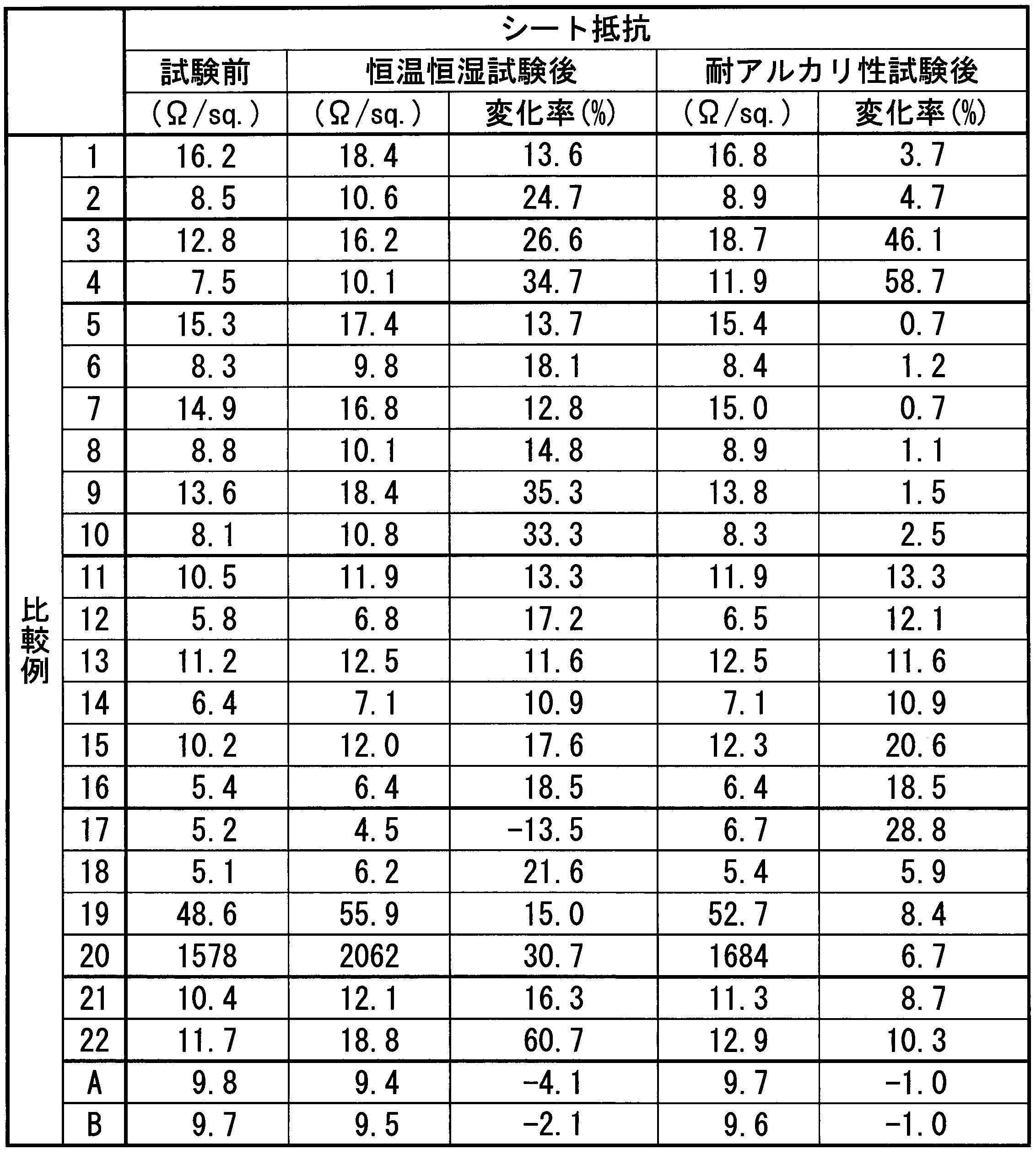
- Sheet resistance was measured by a four-probe method using a surface resistance measuring instrument (Loresta AP MCP-T400 manufactured by Mitsubishi Yuka Co., Ltd.).
- ⁇ Transmissivity> Using a spectrophotometer (U4100 manufactured by Hitachi High-Technologies Corporation), a transmittance spectrum in a wavelength range of 400 nm to 800 nm was measured, and an average transmittance (transmittance) was obtained.
- ⁇ Constant temperature and humidity test> The sample was left in a constant temperature and humidity chamber of 85 ° C. and 85% humidity for 250 hours, and the transmittance and sheet resistance after the test were measured to evaluate the rate of change from before the test.
- ⁇ Alkali resistance test> The film was immersed in an alkaline resist removing solution (pH 9, TOK-104 manufactured by Tokyo Ohka Kogyo Co., Ltd.) at a temperature of 40 ° C. for 10 minutes, and the transmittance and sheet resistance after immersion were measured to evaluate the rate of change from before immersion.
- an alkaline resist removing solution pH 9, TOK-104 manufactured by Tokyo Ohka Kogyo Co., Ltd.
- ⁇ Patterning test by etching method About the above-mentioned laminated transparent conductive film, a resist film was formed on the laminated transparent conductive film in a wiring pattern shape of line width / space width: 30 ⁇ m / 30 ⁇ m by photolithography. This was batch etched using a mixed solution containing phosphoric acid and acetic acid (SEA-5 manufactured by Kanto Chemical Co., Inc.) as an etchant. The etching was performed without heating and with an appropriate etching time (20 seconds to 120 seconds). Further, the phosphoric acid content in the mixed solution was 55% by volume or less, and the acetic acid content was 30% by volume or less.
- SEA-5 manufactured by Kanto Chemical Co., Inc.
- FIG. 7A shows the observation result of Example 4 of the present invention
- FIG. 7B shows the observation result of Comparative Example 12.
- ⁇ Patterning test by lift-off method First, a resist solution is applied to the substrate, a photomask on which a wiring pattern of line width / space width: 30 ⁇ m / 30 ⁇ m is formed, exposed to ultraviolet rays with an exposure machine, and then the portion exposed to the developer is removed. Then, a reversal pattern was formed by photolithography. Next, a laminated transparent conductive film was formed on the substrate on which the reverse pattern was formed using the sputtering apparatus as described above. Next, after immersing in a resist removing solution to remove the laminated transparent conductive film formed on the resist film, the formed wiring pattern was observed with an optical microscope.
- the average transmittance after film formation exceeds 85%, and the sheet resistance after film formation is 10 ⁇ / sq. It was confirmed that a laminated transparent conductive film having excellent transmittance and sufficiently low resistance was obtained.
- the average transmittance after film formation is 85% or less, and the sheet resistance after film formation is higher than that of the present invention example when compared with the samples having the same composition and film thickness of the Ag film. It was. It is presumed that Ag aggregation occurred in the Ag film.
- the sheet resistance is 10 ⁇ / sq.
- the sheet resistance is 10 ⁇ / sq.
- the average transmittance was greatly deteriorated to 76.4%.
- Comparative Example B by heating the glass substrate to 200 ° C., the film thickness is 180 nm and the sheet resistance is 10 ⁇ / sq. The average transmittance was 85% or less.
- the transmittance after the alkali resistance test and the change rate of the sheet resistance are small, the average transmittance after the test is 85% or more, and the alkali resistance is excellent. confirmed.
- the comparative example many samples with a large change rate of transmittance or sheet resistance after the alkali resistance test were observed, and many samples had insufficient alkali resistance. Even in the samples having a small change rate, the average transmittance after the test was 85% or less.
- the wiring pattern can be formed with high accuracy in the example of the present invention.
Landscapes
- Engineering & Computer Science (AREA)
- Chemical & Material Sciences (AREA)
- Physics & Mathematics (AREA)
- General Engineering & Computer Science (AREA)
- Theoretical Computer Science (AREA)
- Mechanical Engineering (AREA)
- Metallurgy (AREA)
- Organic Chemistry (AREA)
- Chemical Kinetics & Catalysis (AREA)
- Nonlinear Science (AREA)
- Materials Engineering (AREA)
- General Physics & Mathematics (AREA)
- Manufacturing & Machinery (AREA)
- Mathematical Physics (AREA)
- Crystallography & Structural Chemistry (AREA)
- Human Computer Interaction (AREA)
- Optics & Photonics (AREA)
- Non-Insulated Conductors (AREA)
- Laminated Bodies (AREA)
Abstract
AgまたはAg合金よりなるAg膜(12)と、Ag膜(12)の両面に配置された透明導電酸化物膜(11、13)と、を有し、透明導電酸化物膜(11、13)は、Zn、Ga、Y及びSnを含む酸化物からなることを特徴とする。波長400~800nmの可視光域の平均透過率が85%以上、シート抵抗値が10Ω/sq.以下であることが好ましい。
Description
本願発明は、例えばディスプレイあるいはタッチパネル等の透明電極膜として使用可能な積層透明導電膜、この積層透明導電膜からなる積層配線膜及び積層配線膜の製造方法に関するものである。
本願は、2016年1月28日に日本に出願された特願2016-014703号及び2017年1月12日に日本に出願された特願2017-003349号に基づき優先権を主張し、その内容をここに援用する。
本願は、2016年1月28日に日本に出願された特願2016-014703号及び2017年1月12日に日本に出願された特願2017-003349号に基づき優先権を主張し、その内容をここに援用する。
液晶ディスプレイ、有機ELディスプレイ、及び、タッチパネル等においては、透明電極膜として、例えば特許文献1-4に示すような透明導電膜が提供されている。この透明導電膜には、可視光域の光の透過率が高く、かつ、電気抵抗の低いものが要求される。
ここで、特許文献1においては、透明導電膜として、透明導電酸化物の一種であるITO(In2O3+Sn)からなるITO膜が用いられているが、このITO膜において電気抵抗を低くするためには、膜厚を厚く形成する必要があるため、可視光域の透過率が低下してしまう。よって、高い透過率と低い電気抵抗を両立することが困難であった。
また、特許文献2においては、Cuなどのメタルメッシュ材が用いられているが、このメタルメッシュ材において電気抵抗を低くするためには、メタル部分の幅を広くする必要があり、やはり透過率が低下してしまうといった問題があった。また、光の反射によってメタルメッシュ材が視認されるおそれがあることから、メタルメッシュ材の表面に黒色化膜等を形成する必要があった。
特許文献3、4には、Ag膜と透明導電酸化物膜とを積層した積層透明導電膜が提案されている。この積層透明導電膜においては、Ag膜によって導電性が確保されていることから、電気抵抗を低くするために透明導電酸化物膜を厚く形成する必要がなくなり、比較的高い透過率を得ることが可能となる。
ところで、最近では、ディスプレイあるいはタッチパネル等においては、配線及び透明電極の微細化がさらに進められており、さらに、大画面化によって配線及び透明電極の長さが長くなってきており、透明電極として、従来にも増して電気抵抗が低く、かつ、可視光域の透過率に優れた透明導電膜が求められている。
ここで、特許文献3、4に記載された積層透明導電膜において、さらなる電気抵抗の低下及び透過率の向上を図るためには、Ag膜の膜厚を薄くする必要がある。しかしながら、単にAg膜を薄くした場合には、Agが凝集しやすくなり、このAgの凝集によって表面プラズモン吸収が発生し、透過率が大幅に低下してしまうといった問題があった。また、Agの凝集によってAg膜が不連続膜となるため、電気抵抗も増加して導電性が低下してしまうといった問題があった。
ここで、特許文献3、4に記載された積層透明導電膜において、さらなる電気抵抗の低下及び透過率の向上を図るためには、Ag膜の膜厚を薄くする必要がある。しかしながら、単にAg膜を薄くした場合には、Agが凝集しやすくなり、このAgの凝集によって表面プラズモン吸収が発生し、透過率が大幅に低下してしまうといった問題があった。また、Agの凝集によってAg膜が不連続膜となるため、電気抵抗も増加して導電性が低下してしまうといった問題があった。
また、透明導電酸化物膜の水分に対するバリア性が低いと、湿度の高い環境下で水分がAg膜にまで到達し、Ag膜においてAgの凝集が促進され、透過率及び導電性が低下してしまうおそれがあった。
さらに、上述の積層透明導電膜を配線膜として使用するためには、積層透明導電膜に対して配線パターンを形成する必要がある。この場合、レジスト膜を形成して配線パターンを形成した後、このレジスト膜を除去することになる。レジスト膜を除去する際には、アルカリ性のレジスト除去液を用いるが、従来の積層透明導電膜においては、耐アルカリ性が不十分であって、レジスト膜を除去する際に、積層透明導電膜の特性が劣化してしまうといった問題があった。
さらに、上述の積層透明導電膜を配線膜として使用するためには、積層透明導電膜に対して配線パターンを形成する必要がある。この場合、レジスト膜を形成して配線パターンを形成した後、このレジスト膜を除去することになる。レジスト膜を除去する際には、アルカリ性のレジスト除去液を用いるが、従来の積層透明導電膜においては、耐アルカリ性が不十分であって、レジスト膜を除去する際に、積層透明導電膜の特性が劣化してしまうといった問題があった。
この発明は、前述した事情に鑑みてなされたものであって、透過率が十分に高く、かつ、電気抵抗が十分に低く、耐環境性及び耐アルカリ性に優れた積層透明導電膜、この積層透明導電膜からなる積層配線膜及び積層配線膜の製造方法を提供することを目的とする。
上記課題を解決するために、本願発明の一態様の積層透明導電膜(以下、「本願発明の積層透明導電膜」と称する)は、AgまたはAg合金よりなるAg膜と、前記Ag膜の両面に配置された透明導電酸化物膜と、を有し、前記透明導電酸化物膜は、Zn、Ga、Y及びSnを含む酸化物からなることを特徴とする。
本願発明の積層透明導電膜によれば、Ag膜の両面にZn、Ga、Y及びSnを含む酸化物からなる透明導電酸化物膜が形成されているので、下面の透明導電酸化物膜によって、Ag膜の濡れ性が向上することになり、Ag膜を薄く形成した場合であってもAg膜におけるAgの凝集を抑制することができる。また、上述の透明導電酸化物膜は、耐環境性(高温高湿下環境における耐久性)に優れていることから、湿度の高い環境下で使用した場合であっても、Ag膜の上面に形成された透明導電酸化物膜によって、Ag膜への水分の侵入を抑制でき、Agの凝集を抑制することができる。よって、透過率が十分に高く、かつ、電気抵抗が十分に低い透明導電酸化物膜を提供することができる。
さらに、リン酸、酢酸を含む酸性の混合液をエッチャントとして使用した場合には、Ag膜と透明導電酸化物膜とのエッチング速度の差が小さく、この積層透明導電膜を一括エッチングしても精度良く配線パターンを形成することができる。
また、この透明導電酸化物膜は耐アルカリ性が高いので、配線パターンを形成する際、アルカリ性のレジスト除去液を用いてレジスト膜を除去しても、積層透明導電膜の特性の劣化を抑制することができる。
さらに、リン酸、酢酸を含む酸性の混合液をエッチャントとして使用した場合には、Ag膜と透明導電酸化物膜とのエッチング速度の差が小さく、この積層透明導電膜を一括エッチングしても精度良く配線パターンを形成することができる。
また、この透明導電酸化物膜は耐アルカリ性が高いので、配線パターンを形成する際、アルカリ性のレジスト除去液を用いてレジスト膜を除去しても、積層透明導電膜の特性の劣化を抑制することができる。
ここで、本願発明の積層透明導電膜においては、前記透明導電酸化物膜中に含まれる全金属元素の原子割合が、Ga;0.9原子%以上26.1原子%以下、Y;0.2原子%以上9.5原子%以下、Sn;0.1原子%以上4.7原子%以下、残Znとされていることが好ましい。
この場合、透明導電酸化物膜中に含まれる全金属元素におけるGaの含有量が0.9原子%以上26.1原子%以下の範囲内とされているので、電気抵抗の増加を抑制することができる。また、Yの含有量が0.2原子%以上9.5原子%以下の範囲内とされているので、電気抵抗の増加を抑制しつつ耐アルカリ性を向上させることができる。さらに、Snの含有量が0.1原子%以上4.7原子%以下の範囲内とされているので、電気抵抗の増加を抑制しつつ耐環境性を向上させることができる。
この場合、透明導電酸化物膜中に含まれる全金属元素におけるGaの含有量が0.9原子%以上26.1原子%以下の範囲内とされているので、電気抵抗の増加を抑制することができる。また、Yの含有量が0.2原子%以上9.5原子%以下の範囲内とされているので、電気抵抗の増加を抑制しつつ耐アルカリ性を向上させることができる。さらに、Snの含有量が0.1原子%以上4.7原子%以下の範囲内とされているので、電気抵抗の増加を抑制しつつ耐環境性を向上させることができる。
また、本願発明の積層透明導電膜においては、前記Ag膜は、Cu、Sn、Sb、Ti、Mg、Zn、Ge、In、Al、Ga、Pd、Au、Pt、Bi、Mn、Sc、Y、Nd、Sm、Eu、Gd、Tb、Erのうちの1種又は2種以上を合計で0.2原子%以上10.0原子%以下含有し、残部がAg及び不可避不純物からなるAg合金で構成されていることが好ましい。
この場合、Cu、Sn、Sb、Ti、Mg、Zn、Ge、In、Al、Ga、Pd、Au、Pt、Bi、Mn、Sc、Y、Nd、Sm、Eu、Gd、Tb、Erのうちの1種又は2種以上を含有しているので、Ag膜の凝集がさらに抑制されることになり、Ag膜を10nm以下に極めて薄く形成しても、連続膜とすることができる。
この場合、Cu、Sn、Sb、Ti、Mg、Zn、Ge、In、Al、Ga、Pd、Au、Pt、Bi、Mn、Sc、Y、Nd、Sm、Eu、Gd、Tb、Erのうちの1種又は2種以上を含有しているので、Ag膜の凝集がさらに抑制されることになり、Ag膜を10nm以下に極めて薄く形成しても、連続膜とすることができる。
さらに、本願発明の積層透明導電膜においては、前記Ag膜の厚さが10nm以下とされていることが好ましい。
この場合、Ag膜の厚さが10nm以下とされているので、透過率を向上させることができる。また、Ag膜の両面に上述の透明導電酸化物膜が形成されているので、Ag膜の厚さが10nm以下としても、Agの凝集がなく連続膜となるため、電気抵抗を低くすることができる。
この場合、Ag膜の厚さが10nm以下とされているので、透過率を向上させることができる。また、Ag膜の両面に上述の透明導電酸化物膜が形成されているので、Ag膜の厚さが10nm以下としても、Agの凝集がなく連続膜となるため、電気抵抗を低くすることができる。
また、本願発明の積層透明導電膜においては、波長400~800nmの可視光域の平均透過率が85%以上、シート抵抗値が10Ω/sq.(square)以下であることが好ましい。
この場合、可視光域の平均透過率が85%以上、かつ、シート抵抗値が10Ω/sq.以下とされているので、十分に高い透過率及び十分に低い電気抵抗を有しており、微細化された透明電極膜又は透明配線膜として使用することができる。
この場合、可視光域の平均透過率が85%以上、かつ、シート抵抗値が10Ω/sq.以下とされているので、十分に高い透過率及び十分に低い電気抵抗を有しており、微細化された透明電極膜又は透明配線膜として使用することができる。
本願発明の他態様の積層配線膜(以下、「本願発明の積層配線膜」と称する)は、上述の積層透明導電膜からなり、配線パターンを有することを特徴とする。
本願発明の積層配線膜によれば、上述の積層透明導電膜からなることから、低い電気抵抗と高い透過率を有する。
本願発明の積層配線膜によれば、上述の積層透明導電膜からなることから、低い電気抵抗と高い透過率を有する。
本願発明の他態様の積層配線膜の製造方法(以下、「本願発明の積層配線膜の製造方法」と称する)は、上述の積層配線膜の製造方法であって、基材の成膜面に、前記Ag膜及び前記透明導電酸化物膜を含む前記積層透明導電膜を成膜する積層透明導電膜成膜工程と、前記積層透明導電膜の上に配線パターン状のレジスト膜を形成するレジスト膜形成工程と、前記レジスト膜が形成された前記積層透明導電膜に対して、リン酸、酢酸を含む酸性の混合液をエッチャントに用いて、エッチングを一括して行うエッチング工程と、エッチング後にアルカリ性のレジスト除去液で前記レジスト膜を除去するレジスト膜除去工程と、を備えていることを特徴とする。
この構成の積層配線膜の製造方法によれば、リン酸、酢酸を含む酸性の混合液をエッチャントとして使用した場合に、Ag膜と透明導電酸化物膜とのエッチング速度の差が小さいことから、この積層透明導電膜を一括エッチングしても、Ag膜のオーバーエッチングOEや透明導電酸化物膜の残渣R等が発生することが抑制でき、精度良く配線パターンを形成することができる。また、Yの添加によって透明導電酸化物膜の耐アルカリ性が向上しているので、レジスト膜除去工程において、アルカリ性のレジスト除去液を用いてレジスト膜を除去しても、積層配線膜の特性の劣化を抑制することができる。
また、本願発明の積層配線膜の製造方法は、上述の積層配線膜の製造方法であって、基材の成膜面に配線パターンの反転パターン状のレジスト膜を形成するレジスト膜形成工程と、前記レジスト膜が形成された前記基材の成膜面に、前記Ag膜及び前記透明導電酸化物膜を含む前記積層透明導電膜を成膜する積層透明導電膜成膜工程と、前記レジスト膜を除去するレジスト膜除去工程と、を備えていることを特徴とする。
この構成の積層配線膜の製造方法によれば、基材の成膜面にレジスト膜を配線パターンの反転パターン状に形成し、前記レジスト膜が形成された前記基材の成膜面に前記積層透明導電膜を成膜している。これにより、前記積層透明導電膜を成膜した後に、レジスト膜を基材から除去すると、レジスト膜が形成されていなかった領域にのみ前記積層透明導電膜が残存し、配線パターンを有する積層配線膜を形成することが可能となる。このため、エッチング工程を行う必要がなく、配線パターンを精度良く形成することができる。また、Yの添加によって透明導電酸化物膜の耐アルカリ性が向上しているので、レジスト膜除去工程において、アルカリ性のレジスト除去液を用いてレジスト膜を除去しても、積層配線膜の特性の劣化を抑制することができる。
本願発明の積層透明導電膜によれば、透過率が十分に高く、かつ、電気抵抗が十分に低く、耐環境性及び耐アルカリ性に優れた積層透明導電膜、この積層透明導電膜からなる積層配線膜及び積層配線膜の製造方法を提供することが可能となる。
以下に、本願発明の実施形態である積層透明導電膜について、添付した図を参照して説明する。
本実施形態における積層透明導電膜10は、各種ディスプレイ及びタッチパネルの透明電極膜として使用されるものであり、特に、タブレットサイズ以上の静電容量タイプのタッチパネルにおいて使用されるものとされている。
本実施形態における積層透明導電膜10は、各種ディスプレイ及びタッチパネルの透明電極膜として使用されるものであり、特に、タブレットサイズ以上の静電容量タイプのタッチパネルにおいて使用されるものとされている。
本実施形態である積層透明導電膜10を図1に示す。この積層透明導電膜10は、例えば基板20の一面に下地層として成膜された第1透明導電酸化物膜11と、この第1透明導電酸化物膜11上に成膜されたAg膜12と、このAg膜12上に成膜された第2透明導電酸化物膜13と、を備えている。なお、基板20としては、例えばガラス基板、樹脂フィルム等を用いることができる。
そして、本実施形態においては、積層透明導電膜10は、波長400~800nmの可視光域の平均透過率が85%以上、シート抵抗値が10Ω/sq.以下とされている。
なお、積層透明導電膜10の波長400~800nmの可視光域の平均透過率は85%以上であることが好ましく、86%以上であることがさらに好ましい。また、積層透明導電膜10のシート抵抗値は10Ω/sq.以下であることが好ましく、5Ω/sq.以下であることがさらに好ましい。
なお、積層透明導電膜10の波長400~800nmの可視光域の平均透過率は85%以上であることが好ましく、86%以上であることがさらに好ましい。また、積層透明導電膜10のシート抵抗値は10Ω/sq.以下であることが好ましく、5Ω/sq.以下であることがさらに好ましい。
Ag膜12は、Ag又はAg合金で構成されている。Ag膜12を構成するAg又はAg合金としては、純度が99.9質量%以上の純Ag、あるいは、Cu、Sn、Sb、Zn、Ge、In、Al、Ga、Ti、Mg、Pd、Au、Pt、Bi、Mn、Sc、Y、Nd、Sm、Eu、Gd、Tb、Er等の添加元素を含むAg合金であってもよい。なお、添加元素の含有量は、Ag膜12の吸収率の増加(透過率の低下)及び電気抵抗の増加を抑制する観点から、10.0原子%以下に制限することが望ましく、2.0原子%以下であることがさらに好ましい。
なお、本実施形態では、Cu、Sn、Sb、Zn、Ge、In、Al、Ga、Ti、Mg、Pd、Au、Pt、Bi、Mn、Sc、Y、Nd、Sm、Eu、Gd、Tb、Erのうちの1種又は2種以上を合計で0.2原子%以上10.0原子%以下含有し、残部がAg及び不可避不純物からなるAg合金で構成されたものとされている。
なお、本実施形態では、Cu、Sn、Sb、Zn、Ge、In、Al、Ga、Ti、Mg、Pd、Au、Pt、Bi、Mn、Sc、Y、Nd、Sm、Eu、Gd、Tb、Erのうちの1種又は2種以上を合計で0.2原子%以上10.0原子%以下含有し、残部がAg及び不可避不純物からなるAg合金で構成されたものとされている。
本実施形態において、Ag膜12を構成するAg合金が含有するCu、Sn、Sb、Zn、Ge、In、Al、Ga、Ti、Mg、Pd、Au、Pt、Bi、Mn、Sc、Y、Nd、Sm、Eu、Gd、Tb、Erは、Ag膜12の第1透明導電酸化物膜11に対する濡れ性を向上させる作用効果を有する元素であり、Ag膜12を薄く形成した場合であってもAgの凝集を抑制することが可能となる。
ここで、Cu、Sn、Sb、Zn、Ge、In、Al、Ga、Ti、Mg、Pd、Au、Pt、Bi、Mn、Sc、Y、Nd、Sm、Eu、Gd、Tb、Erのうちの1種又は2種以上の合計含有量が0.2原子%未満の場合には、上述の作用効果を十分に奏功せしめることができないおそれがある。一方、Cu、Sn、Sb、Zn、Ge、In、Al、Ga、Ti、Mg、Pd、Au、Pt、Bi、Mn、Sc、Y、Nd、Sm、Eu、Gd、Tb、Erのうちの1種又は2種以上の合計含有量が10.0原子%を超えるとAg膜12の透過率が低下し、かつ、抵抗値が上昇するおそれがある。
このような理由から、本実施形態では、Ag膜12を構成するAg合金におけるCu、Sn、Sb、Zn、Ge、In、Al、Ga、Ti、Mg、Pd、Au、Pt、Bi、Mn、Sc、Y、Nd、Sm、Eu、Gd、Tb、Erのうちの1種又は2種以上の合計含有量を0.2原子%以上10.0原子%以下の範囲内に規定している。
ここで、Cu、Sn、Sb、Zn、Ge、In、Al、Ga、Ti、Mg、Pd、Au、Pt、Bi、Mn、Sc、Y、Nd、Sm、Eu、Gd、Tb、Erのうちの1種又は2種以上の合計含有量が0.2原子%未満の場合には、上述の作用効果を十分に奏功せしめることができないおそれがある。一方、Cu、Sn、Sb、Zn、Ge、In、Al、Ga、Ti、Mg、Pd、Au、Pt、Bi、Mn、Sc、Y、Nd、Sm、Eu、Gd、Tb、Erのうちの1種又は2種以上の合計含有量が10.0原子%を超えるとAg膜12の透過率が低下し、かつ、抵抗値が上昇するおそれがある。
このような理由から、本実施形態では、Ag膜12を構成するAg合金におけるCu、Sn、Sb、Zn、Ge、In、Al、Ga、Ti、Mg、Pd、Au、Pt、Bi、Mn、Sc、Y、Nd、Sm、Eu、Gd、Tb、Erのうちの1種又は2種以上の合計含有量を0.2原子%以上10.0原子%以下の範囲内に規定している。
なお、上述の作用効果を確実に奏功せしめるためには、Ag膜12を構成するAg合金におけるCu、Sn、Sb、Zn、Ge、In、Al、Ga、Ti、Mg、Pd、Au、Pt、Bi、Mn、Sc、Y、Nd、Sm、Eu、Gd、Tb、Erのうちの1種又は2種以上の合計含有量の下限を0.5原子%以上とすることが好ましい。
一方、透過率の低下や抵抗率の上昇をさらに抑制するためには、Cu、Sn、Sb、Zn、Ge、In、Al、Ga、Ti、Mg、Pd、Au、Pt、Bi、Mn、Sc、Y、Nd、Sm、Eu、Gd、Tb、Erのうちの1種又は2種以上の合計含有量の上限を2.0原子%以下とすることが好ましい。
一方、透過率の低下や抵抗率の上昇をさらに抑制するためには、Cu、Sn、Sb、Zn、Ge、In、Al、Ga、Ti、Mg、Pd、Au、Pt、Bi、Mn、Sc、Y、Nd、Sm、Eu、Gd、Tb、Erのうちの1種又は2種以上の合計含有量の上限を2.0原子%以下とすることが好ましい。
さらに、上述の作用効果を確実に奏功せしめるためには、Ag膜12を構成するAg合金が、上述の添加元素のうちCu、Sn、Sbの少なくとも1種または2種以上を含有することが好ましい。このとき、Cu、Sn、Sbの少なくとも1種または2種以上の含有量は、0.2原子%以上2.0原子%以下の範囲内とすることが好ましい。
そして、本実施形態においては、第1透明導電酸化物膜11及び第2透明導電酸化物膜13は、Zn、Ga、Y及びSnを含む酸化物、すなわち、Zn酸化物にGa、Y及びSnが添加されたものとされている。
本実施形態では、第1透明導電酸化物膜11及び第2透明導電酸化物膜13は、それぞれの透明導電酸化物膜中に含まれる全金属元素におけるGa、Y及びSnの原子割合が、Ga;0.9原子%以上26.1原子%以下、Y;0.2原子%以上9.5原子%以下、Sn;0.1原子%以上4.7原子%以下とされている。
なお、第1透明導電酸化物膜11及び第2透明導電酸化物膜13は同一の組成である必要はなく、上述の組成の範囲内とされていればよい。
本実施形態では、第1透明導電酸化物膜11及び第2透明導電酸化物膜13は、それぞれの透明導電酸化物膜中に含まれる全金属元素におけるGa、Y及びSnの原子割合が、Ga;0.9原子%以上26.1原子%以下、Y;0.2原子%以上9.5原子%以下、Sn;0.1原子%以上4.7原子%以下とされている。
なお、第1透明導電酸化物膜11及び第2透明導電酸化物膜13は同一の組成である必要はなく、上述の組成の範囲内とされていればよい。
ここで、第1透明導電酸化物膜11及び第2透明導電酸化物膜13中に含まれる全金属元素におけるGaの含有量を0.9原子%以上とすることにより、Ag膜12におけるAgの凝集を抑制することができ、積層透明導電膜10における電気抵抗の増加を抑制することができる。一方、Gaの含有量を26.1原子%以下とすることにより、第1透明導電酸化物膜11及び第2透明導電酸化物膜13における電気抵抗の増加を抑制することができる。
なお、Ag膜12におけるAgの凝集を抑制するためには、Gaの含有量の下限を0.9原子%以上とすることが好ましく、2.0原子%以上とすることがさらに好ましい。また、第1透明導電酸化物膜11及び第2透明導電酸化物膜13における電気抵抗の増加を確実に抑制するためには、Gaの含有量の上限を26.1原子%以下とすることが好ましく、20.0原子%以下とすることがさらに好ましい。
なお、Ag膜12におけるAgの凝集を抑制するためには、Gaの含有量の下限を0.9原子%以上とすることが好ましく、2.0原子%以上とすることがさらに好ましい。また、第1透明導電酸化物膜11及び第2透明導電酸化物膜13における電気抵抗の増加を確実に抑制するためには、Gaの含有量の上限を26.1原子%以下とすることが好ましく、20.0原子%以下とすることがさらに好ましい。
また、第1透明導電酸化物膜11及び第2透明導電酸化物膜13中に含まれる全金属元素におけるYの含有量を0.2原子%以上とすることにより、第1透明導電酸化物膜11及び第2透明導電酸化物膜13の耐アルカリ性を向上させることができる。一方、Yの含有量を9.5原子%以下とすることにより、第1透明導電酸化物膜11及び第2透明導電酸化物膜13における電気抵抗の増加を抑制することができる。
なお、第1透明導電酸化物膜11及び第2透明導電酸化物膜13の耐アルカリ性を確実に向上させるためには、Yの含有量の下限を0.2原子%以上とすることが好ましく、1.0原子%以上とすることがさらに好ましい。また、第1透明導電酸化物膜11及び第2透明導電酸化物膜13における電気抵抗の増加を確実に抑制するためには、Yの含有量の上限を9.5原子%以下とすることが好ましく、8.0原子%以下とすることがさらに好ましい。
なお、第1透明導電酸化物膜11及び第2透明導電酸化物膜13の耐アルカリ性を確実に向上させるためには、Yの含有量の下限を0.2原子%以上とすることが好ましく、1.0原子%以上とすることがさらに好ましい。また、第1透明導電酸化物膜11及び第2透明導電酸化物膜13における電気抵抗の増加を確実に抑制するためには、Yの含有量の上限を9.5原子%以下とすることが好ましく、8.0原子%以下とすることがさらに好ましい。
さらに、第1透明導電酸化物膜11及び第2透明導電酸化物膜13中に含まれる全金属元素におけるSnの含有量を0.1原子%以上とすることにより、透明導電酸化物膜の耐環境性を向上させることができる。一方、Snの含有量を4.7原子%以下とすることにより、第1透明導電酸化物膜11及び第2透明導電酸化物膜13における電気抵抗の増加を抑制することができる。
なお、第1透明導電酸化物膜11及び第2透明導電酸化物膜13の耐環境性を確実に向上させるためには、Snの含有量の下限を0.1原子%以上とすることが好ましく、0.5原子%以上とすることがさらに好ましい。また、第1透明導電酸化物膜11及び第2透明導電酸化物膜13における電気抵抗の増加を確実に抑制するためには、Snの含有量の上限を4.7原子%以下とすることが好ましく、4.0原子%以下とすることがさらに好ましい。
なお、第1透明導電酸化物膜11及び第2透明導電酸化物膜13の耐環境性を確実に向上させるためには、Snの含有量の下限を0.1原子%以上とすることが好ましく、0.5原子%以上とすることがさらに好ましい。また、第1透明導電酸化物膜11及び第2透明導電酸化物膜13における電気抵抗の増加を確実に抑制するためには、Snの含有量の上限を4.7原子%以下とすることが好ましく、4.0原子%以下とすることがさらに好ましい。
また、第1透明導電酸化物膜11及び第2透明導電酸化物膜13における電気抵抗の増加を確実に抑制するためには、Ga、Y及びSnの合計含有量を37.5原子%以下とすることが好ましく、30.0原子%以下とすることが好ましい。
ここで、本実施形態では、透過率を向上させるために、Ag膜12の膜厚t2を10nm以下に設定している。なお、さらなる透過率の向上を図る場合には、Ag膜12の膜厚t2を10nm以下とすることが好ましく、8nm以下とすることがさらに好ましい。また、Ag膜12の膜厚t2の下限は3nm以上とすることが好ましく、4nm以上とすることがさらに好ましい。
そして、第1透明導電酸化物膜11の膜厚t1と第2透明導電酸化物膜13の膜厚t3は、各単相膜での光学定数(屈折率及び消衰係数)を用いて、第1透明導電酸化物膜/Ag膜(Ag合金膜)/第2透明導電酸化物膜の3層構造で光学シミュレーションを行い、可視光域の透過率が光学的干渉効果によって向上する膜厚としている。
第1透明導電酸化物膜11の膜厚t1及び第2透明導電酸化物膜13の膜厚t3は、およそ以下のような範囲の膜厚とすることが好ましい。
t1=550/(4×n1)×k1、t3=550/(4×n3)×k3
ここで、n1、n3は、第1透明導電酸化物膜11の屈折率(n1)及び第2透明導電酸化物膜13の屈折率(n3)である。また、k1、k3は、第1透明導電酸化物膜11の係数(k1)及び第2透明導電酸化物膜13の係数(k3)である。
t1=550/(4×n1)×k1、t3=550/(4×n3)×k3
ここで、n1、n3は、第1透明導電酸化物膜11の屈折率(n1)及び第2透明導電酸化物膜13の屈折率(n3)である。また、k1、k3は、第1透明導電酸化物膜11の係数(k1)及び第2透明導電酸化物膜13の係数(k3)である。
なお、係数k1、k3は、透明導電酸化物によってそれぞれ最適値が異なるが、係数k1、k3は、0.2~0.8の範囲であることが好ましく、0.4~0.7の範囲であることがさらに好ましい。特に、係数k1、k3が0.6程度であると、透明導電酸化物の種類によらず可視光域の透過率が向上することになる。
本実施形態では、上述の光学シミュレーションの結果、第1透明導電酸化物膜11の膜厚t1及び第2透明導電酸化物膜13の膜厚t3を40nmに設定している。これらの膜厚は、係数k1、k3を0.6とした場合の膜厚である。
本実施形態では、上述の光学シミュレーションの結果、第1透明導電酸化物膜11の膜厚t1及び第2透明導電酸化物膜13の膜厚t3を40nmに設定している。これらの膜厚は、係数k1、k3を0.6とした場合の膜厚である。
次に、本願発明の実施形態である積層配線膜30及び積層配線膜30の製造方法について、図2から図4を参照して説明する。
本実施形態である積層配線膜30は、図2に示すように、図1に示す積層透明導電膜10に配線パターンが形成されたものである。ここで、本実施形態である積層配線膜30においては、配線パターンは、ラインLの幅及びラインL間のスペースSの幅が1μm以上900μm以下の範囲内である。
本実施形態である積層配線膜30は、図2に示すように、図1に示す積層透明導電膜10に配線パターンが形成されたものである。ここで、本実施形態である積層配線膜30においては、配線パターンは、ラインLの幅及びラインL間のスペースSの幅が1μm以上900μm以下の範囲内である。
ここで、上述の積層配線膜30は、以下のようにして製造される。
まず、基板20の成膜面に、本実施形態である積層透明導電膜10を成膜する(積層透明導電膜成膜工程S11)。
この積層透明導電膜成膜工程S11においては、基板20の上に下地層として第1透明導電酸化物膜11を成膜する。第1透明導電酸化物膜11は、膜組成が制御しやすい焼結ターゲットを用いて、DCスパッタによって成膜することが好ましい。次に、成膜された第1透明導電酸化物膜11の上に、Agターゲットを用いてDCスパッタによってAg膜12を成膜する。このAgターゲットは、成膜されるAg膜12の組成に応じた組成とされている。そして、成膜されたAg膜12の上に、透明導電酸化物ターゲットを用いてDCスパッタによって第2透明導電酸化物膜13を成膜する。なお、透明導電酸化物ターゲットは、膜組成が制御しやすい焼結ターゲットとすることが好ましい。このようにして、本実施形態である積層透明導電膜10を成膜する。
まず、基板20の成膜面に、本実施形態である積層透明導電膜10を成膜する(積層透明導電膜成膜工程S11)。
この積層透明導電膜成膜工程S11においては、基板20の上に下地層として第1透明導電酸化物膜11を成膜する。第1透明導電酸化物膜11は、膜組成が制御しやすい焼結ターゲットを用いて、DCスパッタによって成膜することが好ましい。次に、成膜された第1透明導電酸化物膜11の上に、Agターゲットを用いてDCスパッタによってAg膜12を成膜する。このAgターゲットは、成膜されるAg膜12の組成に応じた組成とされている。そして、成膜されたAg膜12の上に、透明導電酸化物ターゲットを用いてDCスパッタによって第2透明導電酸化物膜13を成膜する。なお、透明導電酸化物ターゲットは、膜組成が制御しやすい焼結ターゲットとすることが好ましい。このようにして、本実施形態である積層透明導電膜10を成膜する。
次に、基板20の表面に成膜された積層透明導電膜10の上にレジスト膜41を形成し、このレジスト膜41に露光・現像することで、配線パターンを形成する(レジスト膜形成工程S12)。
次に、レジスト膜41が形成された積層透明導電膜10に対して、リン酸、酢酸を含む酸性の混合液をエッチャントに用いて、エッチングを一括して行う(エッチング工程S13)。ここで、リン酸、酢酸を含む酸性の混合液においては、リン酸の含有量が55体積%以下、酢酸の含有量が30体積%以下であることが好ましい。
次に、レジスト膜41が形成された積層透明導電膜10に対して、リン酸、酢酸を含む酸性の混合液をエッチャントに用いて、エッチングを一括して行う(エッチング工程S13)。ここで、リン酸、酢酸を含む酸性の混合液においては、リン酸の含有量が55体積%以下、酢酸の含有量が30体積%以下であることが好ましい。
次に、アルカリ性のレジスト除去液を用いて、レジスト膜41を除去する(レジスト膜除去工程S14)。
これにより、配線パターン形状のレジスト膜41の下側に位置する積層透明導電膜10が残り、配線パターンを有する積層配線膜30が形成される。
これにより、配線パターン形状のレジスト膜41の下側に位置する積層透明導電膜10が残り、配線パターンを有する積層配線膜30が形成される。
以上のような構成とされた本実施形態である積層透明導電膜10においては、基板20の表面に下地層として第1透明導電酸化物膜11が形成され、この第1透明導電酸化物膜11の上にAg膜12が成膜されているので、Ag膜12の濡れ性が向上し、Ag膜12を薄く成膜した場合であっても、Agの凝集が抑制される。
さらに、第1透明導電酸化物膜11及び第2透明導電酸化物膜13が、耐環境性に優れていることから、湿度の高い環境下で使用した場合であっても、Ag膜12への水分の侵入を抑制でき、Agの凝集を抑制することができる。
よって、Ag膜12においてAgの凝集による表面プラズモン吸収の発生を防止でき、高い透過率を得ることができる。また、Ag膜12が連続膜となるため、電気抵抗も低くすることができる。
さらに、第1透明導電酸化物膜11及び第2透明導電酸化物膜13が、耐環境性に優れていることから、湿度の高い環境下で使用した場合であっても、Ag膜12への水分の侵入を抑制でき、Agの凝集を抑制することができる。
よって、Ag膜12においてAgの凝集による表面プラズモン吸収の発生を防止でき、高い透過率を得ることができる。また、Ag膜12が連続膜となるため、電気抵抗も低くすることができる。
そして、本実施形態では、第1透明導電酸化物膜11及び第2透明導電酸化物膜13は、Zn酸化物にGa、Y及びSnが添加されたものとされており、それぞれの透明導電酸化物膜中に含まれる全金属元素におけるGa、Y及びSnの原子割合が、Ga;0.9原子%以上26.1原子%以下、Y;0.2原子%以上9.5原子%以下、Sn;0.1原子%以上4.7原子%以下とされているので、Gaの添加によってAgの凝集を抑制することができ、電気抵抗の増加を抑制することができる。また、Yの添加によって耐アルカリ性を向上させることができる。さらに、Snの添加によって耐環境性を向上させることができる。
さらに、本実施形態では、Ag膜12の厚さt2を10nm以下に設定しているので、透過率を向上させることができる。また、基板20の表面に下地層として第1透明導電酸化物膜11が形成されているので、Ag膜12の厚さを10nm以下としてもAgの凝集がなく連続膜となり、電気抵抗を低くすることができる。
また、本実施形態では、Ag膜12を、Cu、Sn、Sb、Zn、Ge、In、Al、Ga、Ti、Mg、Pd、Au、Pt、Bi、Mn、Sc、Y、Nd、Sm、Eu、Gd、Tb、Erのうちの1種又は2種以上を合計で0.2原子%以上10.0原子%以下含有し、残部がAg及び不可避不純物からなるAg合金で構成したものとしているので、Ag膜12の凝集がさらに抑制されることになり、Ag膜12をさらに薄く形成しても連続膜となり、高い透過率と低い抵抗値とを両立することできる。
さらに、本実施形態では、波長400~800nmの可視光域の平均透過率が85%以上、シート抵抗値が10Ω/sq.以下とされており、十分に高い透過率及び低い電気抵抗を有しているので、微細化された透明電極膜又は透明配線膜として使用することができる。
また、本実施形態である積層配線膜30においては、本実施形態である積層透明導電膜10に配線パターンが形成されたものであることから、低い電気抵抗と高い透過率を有している。
さらに、本実施形態においては、エッチング工程S13において、リン酸、酢酸を含む酸性の混合液をエッチャントとして使用した場合に、Ag膜12と第1透明導電酸化物膜11及び第2透明導電酸化物膜13とのエッチング速度の差が小さいことから、この積層透明導電膜10を一括エッチングしても、Ag膜12のオーバーエッチングOEや第1透明導電酸化物膜11及び第2透明導電酸化物膜13の残渣R等が発生することが抑制でき、精度良く配線パターンを形成することができる。
また、本実施形態では、Yの添加によって第1透明導電酸化物膜11及び第2透明導電酸化物膜13の耐アルカリ性が向上されているので、レジスト膜除去工程S14において、アルカリ性のレジスト除去液を用いてレジスト膜を除去しても、積層配線膜30の特性の劣化を抑制することができる。
また、本実施形態では、Yの添加によって第1透明導電酸化物膜11及び第2透明導電酸化物膜13の耐アルカリ性が向上されているので、レジスト膜除去工程S14において、アルカリ性のレジスト除去液を用いてレジスト膜を除去しても、積層配線膜30の特性の劣化を抑制することができる。
以上、本願発明の実施形態について説明したが、本願発明はこれに限定されることはなく、その発明の技術的思想を逸脱しない範囲で適宜変更可能である。
例えば、本実施形態では、Ag膜12をCu、Sn、Sb、Zn、Ge、In、Al、Ga、Ti、Mg、Pd、Au、Pt、Bi、Mn、Sc、Y、Nd、Sm、Eu、Gd、Tb、Erのうちの1種又は2種以上を合計で0.2原子%以上10.0原子%以下含有し、残部がAg及び不可避不純物からなるAg合金で構成したものとして説明したが、これに限定されることはなく、純Agや、Agに固溶する他の金属元素を含有するAg合金であってもよい。
例えば、本実施形態では、Ag膜12をCu、Sn、Sb、Zn、Ge、In、Al、Ga、Ti、Mg、Pd、Au、Pt、Bi、Mn、Sc、Y、Nd、Sm、Eu、Gd、Tb、Erのうちの1種又は2種以上を合計で0.2原子%以上10.0原子%以下含有し、残部がAg及び不可避不純物からなるAg合金で構成したものとして説明したが、これに限定されることはなく、純Agや、Agに固溶する他の金属元素を含有するAg合金であってもよい。
また、本実施形態では、第1透明導電酸化物膜11及び第2透明導電酸化物膜13の膜厚を40nm程度のものとして説明したが、これに限定されることはなく、他の膜厚としてもよい。ただし、本実施形態に記載したように、光学シミュレーションを行い、光干渉効果によって透過率が向上する膜厚を選択することが好ましい。
さらに、本実施形態では、積層配線膜30をエッチング法によって製造するものとして説明したが、これに限定されることはなく、図5及び図6に示すように、積層配線膜30をリフトオフ法によって製造してもよい。
図5及び図6に示す積層配線膜30の製造方法においては、まず、基板20の成膜面にレジスト膜41を成膜し、このレジスト膜41に露光・現像することで、配線パターンを反転させた反転パターンを形成する(レジスト膜形成工程S21)。
図5及び図6に示す積層配線膜30の製造方法においては、まず、基板20の成膜面にレジスト膜41を成膜し、このレジスト膜41に露光・現像することで、配線パターンを反転させた反転パターンを形成する(レジスト膜形成工程S21)。
次に、反転パターンを有するレジスト膜41が形成された基板20上に、スパッタ法により、第1透明導電酸化物膜11、Ag膜12、第2透明導電酸化物膜13を順に成膜する。これにより、レジスト膜41及び基板20上に積層透明導電膜10が形成される(積層透明導電膜成膜工程S22)。
次に、アルカリ性のレジスト除去液を用いて、レジスト膜41を除去する(レジスト膜除去工程S23)。
これにより、反転パターン状のレジスト膜41上に成膜された積層透明導電膜10は除去され、配線パターンを有する積層配線膜30が形成される。
次に、アルカリ性のレジスト除去液を用いて、レジスト膜41を除去する(レジスト膜除去工程S23)。
これにより、反転パターン状のレジスト膜41上に成膜された積層透明導電膜10は除去され、配線パターンを有する積層配線膜30が形成される。
この構成の積層配線膜30の製造方法によれば、エッチング工程を行うことなく、配線パターンを精度良く形成することができる。また、Yの添加によって第1透明導電酸化物膜11及び第2透明導電酸化物膜13の耐アルカリ性が向上されているので、レジスト膜除去工程S23において、アルカリ性のレジスト除去液を用いてレジスト膜を除去しても、積層配線膜30の特性の劣化を抑制することができる。
本願発明に係る積層透明導電膜の作用効果について確認した確認実験の結果について説明する。
ガラス基板(無アルカリガラス:50mm×50mm×1mmt)の表面に、表1-3に示す構造の積層透明導電膜をスパッタリング法により成膜した。なお、比較例A、Bでは、ITO単層膜をスパッタリング法により成膜した。また、比較例Bのみ、ガラス基板を200℃に加熱して成膜した。
なお、比較例において、ITO膜(In2O3にSnを添加した酸化物)の組成はIn:35.6原子%、Sn:3.6原子%、O:60.8原子%である。
GZO膜(ZnOにGaを添加した酸化物)の組成はZn:47.3原子%、Ga:2.2原子%、O:50.5原子%である。
GZTO膜(ZnOにGa、Snを添加した酸化物)の組成は、Zn:40.0原子%、Ga:6.7原子%、Sn:1.1原子%、O:52.2原子%である。
GZYO膜(ZnOにGa、Yを添加した酸化物)の組成は、Zn:39.1原子%、Ga:6.5原子%、Y:2.2原子%、O:52.2原子%である。
ZTYO膜(ZnOにSn、Yを添加した酸化物)の組成は、Zn:40.9原子%、Sn:2.3原子%、Y:4.6原子%、O:52.2原子%である。
GTYO膜(SnO2にGa、Yを添加した酸化物)の組成は、Sn:30.5原子%、Ga:1.7原子%、Y:1.7原子%、O:66.1原子%である。
なお、比較例において、ITO膜(In2O3にSnを添加した酸化物)の組成はIn:35.6原子%、Sn:3.6原子%、O:60.8原子%である。
GZO膜(ZnOにGaを添加した酸化物)の組成はZn:47.3原子%、Ga:2.2原子%、O:50.5原子%である。
GZTO膜(ZnOにGa、Snを添加した酸化物)の組成は、Zn:40.0原子%、Ga:6.7原子%、Sn:1.1原子%、O:52.2原子%である。
GZYO膜(ZnOにGa、Yを添加した酸化物)の組成は、Zn:39.1原子%、Ga:6.5原子%、Y:2.2原子%、O:52.2原子%である。
ZTYO膜(ZnOにSn、Yを添加した酸化物)の組成は、Zn:40.9原子%、Sn:2.3原子%、Y:4.6原子%、O:52.2原子%である。
GTYO膜(SnO2にGa、Yを添加した酸化物)の組成は、Sn:30.5原子%、Ga:1.7原子%、Y:1.7原子%、O:66.1原子%である。
ここで、透明導電酸化物膜の膜厚は、実施の形態で説明した光学シミュレーションを行い、光学的干渉効果によって可視光域の透過率が向上する膜厚を選択し、本発明例においては、すべて40nmとした。
なお、本発明の実施例および比較例におけるAg膜及び透明導電酸化物膜の膜厚は、膜厚計(アルバック社製 DEKTAK)を用いて測定した。
また、透明導電酸化物膜およびAg合金膜の組成は、ICP発光分光装置(日立ハイテクサイエンス社製ICP発光分光分析装置STS-3500DD)を用いて元素の定量分析を行うことにより求めた。
なお、本発明の実施例および比較例におけるAg膜及び透明導電酸化物膜の膜厚は、膜厚計(アルバック社製 DEKTAK)を用いて測定した。
また、透明導電酸化物膜およびAg合金膜の組成は、ICP発光分光装置(日立ハイテクサイエンス社製ICP発光分光分析装置STS-3500DD)を用いて元素の定量分析を行うことにより求めた。
透明導電酸化物膜の作製には、表1-3と上に記載した組成の酸化物焼結体ターゲットを用いた。
Ag膜の作製には、表1-3に記載された組成のAgターゲットを用いた。また、比較例として、Ag膜の代わりにCu膜、Al膜を用いた積層膜透明導電膜を、Cuターゲット、Alターゲットを使用して作製した。
それぞれの膜の成膜条件を以下に示す。
Ag膜の作製には、表1-3に記載された組成のAgターゲットを用いた。また、比較例として、Ag膜の代わりにCu膜、Al膜を用いた積層膜透明導電膜を、Cuターゲット、Alターゲットを使用して作製した。
それぞれの膜の成膜条件を以下に示す。
<透明導電酸化物膜の成膜条件>
スパッタリング装置:DCマグネトロンスパッタ装置(アルバック社製CS-200)磁界強度:1000Gauss(ターゲット直上、垂直成分)
到達真空度:5×10⁻⁵Pa以下
スパッタリングガス:Ar+O2の混合ガス(O2の混合比2%)
スパッタリングガス圧:0.4Pa
スパッタリングパワー:DC100W
スパッタリング装置:DCマグネトロンスパッタ装置(アルバック社製CS-200)磁界強度:1000Gauss(ターゲット直上、垂直成分)
到達真空度:5×10⁻⁵Pa以下
スパッタリングガス:Ar+O2の混合ガス(O2の混合比2%)
スパッタリングガス圧:0.4Pa
スパッタリングパワー:DC100W
<Ag膜、Cu膜、Al膜の成膜条件>
スパッタリング装置:DCマグネトロンスパッタ装置(アルバック社製CS-200)磁界強度:1000Gauss(ターゲット直上、垂直成分)
到達真空度:5×10⁻⁵Pa以下
スパッタリングガス:Ar
スパッタリングガス圧:0.5Pa
スパッタリングパワー:DC100W
スパッタリング装置:DCマグネトロンスパッタ装置(アルバック社製CS-200)磁界強度:1000Gauss(ターゲット直上、垂直成分)
到達真空度:5×10⁻⁵Pa以下
スパッタリングガス:Ar
スパッタリングガス圧:0.5Pa
スパッタリングパワー:DC100W
得られた積層透明導電膜及びITO単層膜について、成膜後のシート抵抗及び透過率を評価した。
また、恒温恒湿試験後のシート抵抗及び透過率、及び、耐アルカリ性試験後のシート抵抗及び透過率を評価した。
さらに、得られた積層透明導電膜について、エッチング法によるパターニング試験、及び、リフトオフ法によるパターニング試験を行った。
評価方法について以下に示す。
また、恒温恒湿試験後のシート抵抗及び透過率、及び、耐アルカリ性試験後のシート抵抗及び透過率を評価した。
さらに、得られた積層透明導電膜について、エッチング法によるパターニング試験、及び、リフトオフ法によるパターニング試験を行った。
評価方法について以下に示す。
<シート抵抗>
表面抵抗測定器(三菱油化社製 Loresta AP MCP-T400)を用いて、四探針法によってシート抵抗を測定した。
<透過率>
分光光度計(日立ハイテクノロジーズ社製 U4100)を用いて、400nmから800nmの波長範囲における透過率スペクトルを測定し、平均透過率(透過率)を求めた。
表面抵抗測定器(三菱油化社製 Loresta AP MCP-T400)を用いて、四探針法によってシート抵抗を測定した。
<透過率>
分光光度計(日立ハイテクノロジーズ社製 U4100)を用いて、400nmから800nmの波長範囲における透過率スペクトルを測定し、平均透過率(透過率)を求めた。
<恒温恒湿試験>
温度85℃、湿度85%の恒温恒湿槽に250時間放置し、試験後の透過率及びシート抵抗を測定して試験前からの変化率を評価した。
温度85℃、湿度85%の恒温恒湿槽に250時間放置し、試験後の透過率及びシート抵抗を測定して試験前からの変化率を評価した。
<耐アルカリ性試験>
温度40℃のアルカリ性のレジスト除去液(pH9、東京応化工業社製TOK-104)に10分浸漬し、浸漬後の透過率及びシート抵抗を測定して、浸漬前からの変化率を評価した。
温度40℃のアルカリ性のレジスト除去液(pH9、東京応化工業社製TOK-104)に10分浸漬し、浸漬後の透過率及びシート抵抗を測定して、浸漬前からの変化率を評価した。
<エッチング法によるパターンニング試験>
上述の積層透明導電膜について、フォトリソ法により積層透明導電膜の上にレジスト膜を、ライン幅/スペース幅:30μm/30μmの配線パターン状に形成した。これを、リン酸、酢酸を含む混合液(関東化学社製SEA-5)をエッチャントに用いて、一括エッチングを行った。なお、エッチングは無加熱でそれぞれ適切なエッチング時間(20秒から120秒)で行った。また、混合液におけるリン酸の含有量を55体積%以下、酢酸の含有量を30体積%以下とした。
その後、アルカリ性のレジスト除去液(pH9、東京応化工業社製TOK-104)を用いてレジスト膜を除去した後、形成された配線パターンを光学顕微鏡(KEYENCE社製レーザーマイクロスコープVK-X200)で観察した。本発明例4の観察結果及び比較例12の観察結果を図7に示す。図7Aが本発明例4の観察結果、図7Bが比較例12の観察結果である。
上述の積層透明導電膜について、フォトリソ法により積層透明導電膜の上にレジスト膜を、ライン幅/スペース幅:30μm/30μmの配線パターン状に形成した。これを、リン酸、酢酸を含む混合液(関東化学社製SEA-5)をエッチャントに用いて、一括エッチングを行った。なお、エッチングは無加熱でそれぞれ適切なエッチング時間(20秒から120秒)で行った。また、混合液におけるリン酸の含有量を55体積%以下、酢酸の含有量を30体積%以下とした。
その後、アルカリ性のレジスト除去液(pH9、東京応化工業社製TOK-104)を用いてレジスト膜を除去した後、形成された配線パターンを光学顕微鏡(KEYENCE社製レーザーマイクロスコープVK-X200)で観察した。本発明例4の観察結果及び比較例12の観察結果を図7に示す。図7Aが本発明例4の観察結果、図7Bが比較例12の観察結果である。
<リフトオフ法によるパターンニング試験>
まず、基板にレジスト液を塗布して、ライン幅/スペース幅:30μm/30μmの配線パターンが形成されたフォトマスクを付けて露光機で紫外線を当てた後、現像液で感光された部分を除去し、フォトリソ法によって反転パターンを形成した。
次に、反転パターンが形成された基板の上に、上述のようにスパッタリング装置を用いて積層透明導電膜を成膜した。
次に、レジスト除去液に浸漬し、レジスト膜の上に成膜された積層透明導電膜を除去した後、形成された配線パターンを光学顕微鏡で観察した。
まず、基板にレジスト液を塗布して、ライン幅/スペース幅:30μm/30μmの配線パターンが形成されたフォトマスクを付けて露光機で紫外線を当てた後、現像液で感光された部分を除去し、フォトリソ法によって反転パターンを形成した。
次に、反転パターンが形成された基板の上に、上述のようにスパッタリング装置を用いて積層透明導電膜を成膜した。
次に、レジスト除去液に浸漬し、レジスト膜の上に成膜された積層透明導電膜を除去した後、形成された配線パターンを光学顕微鏡で観察した。


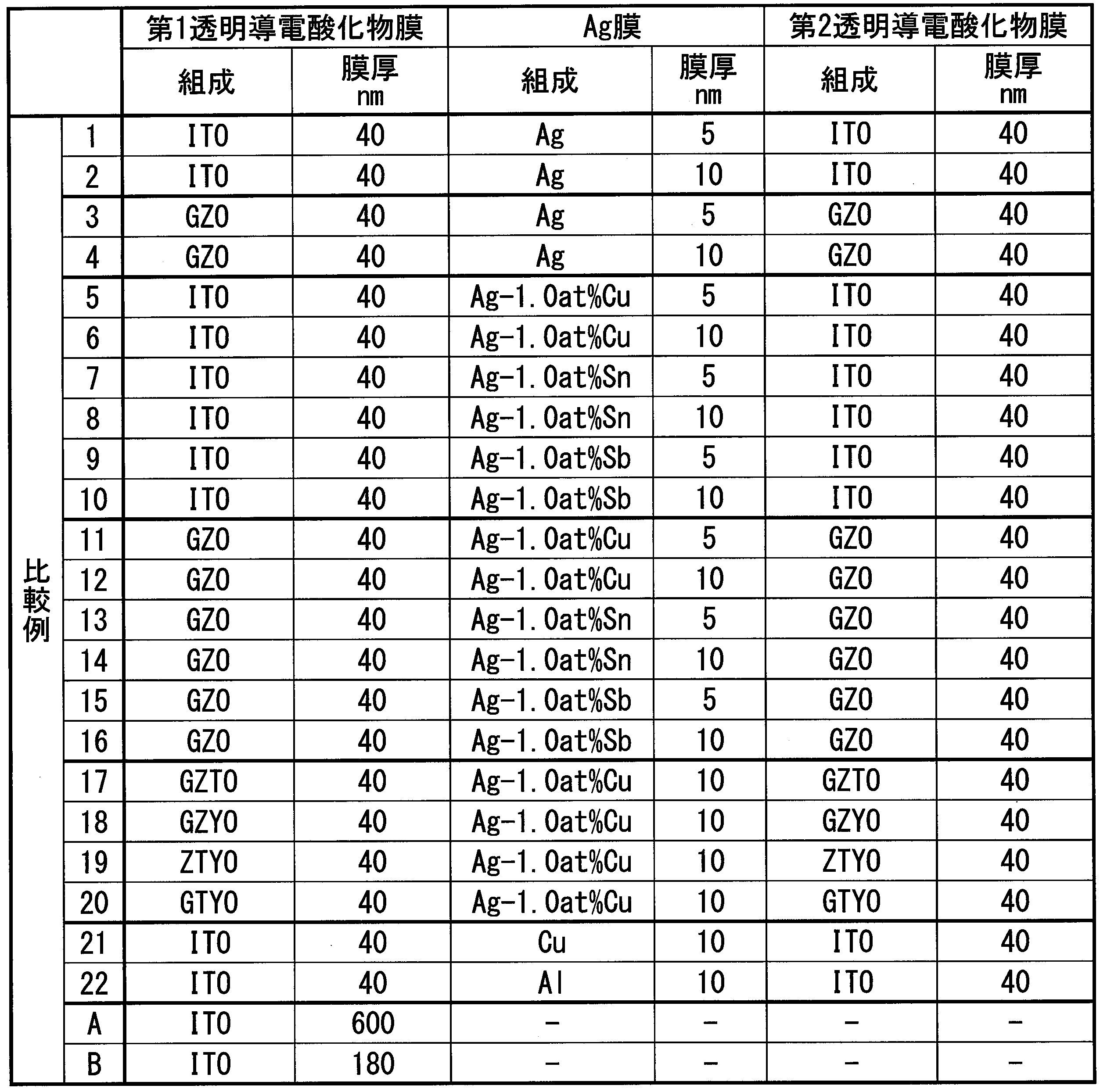

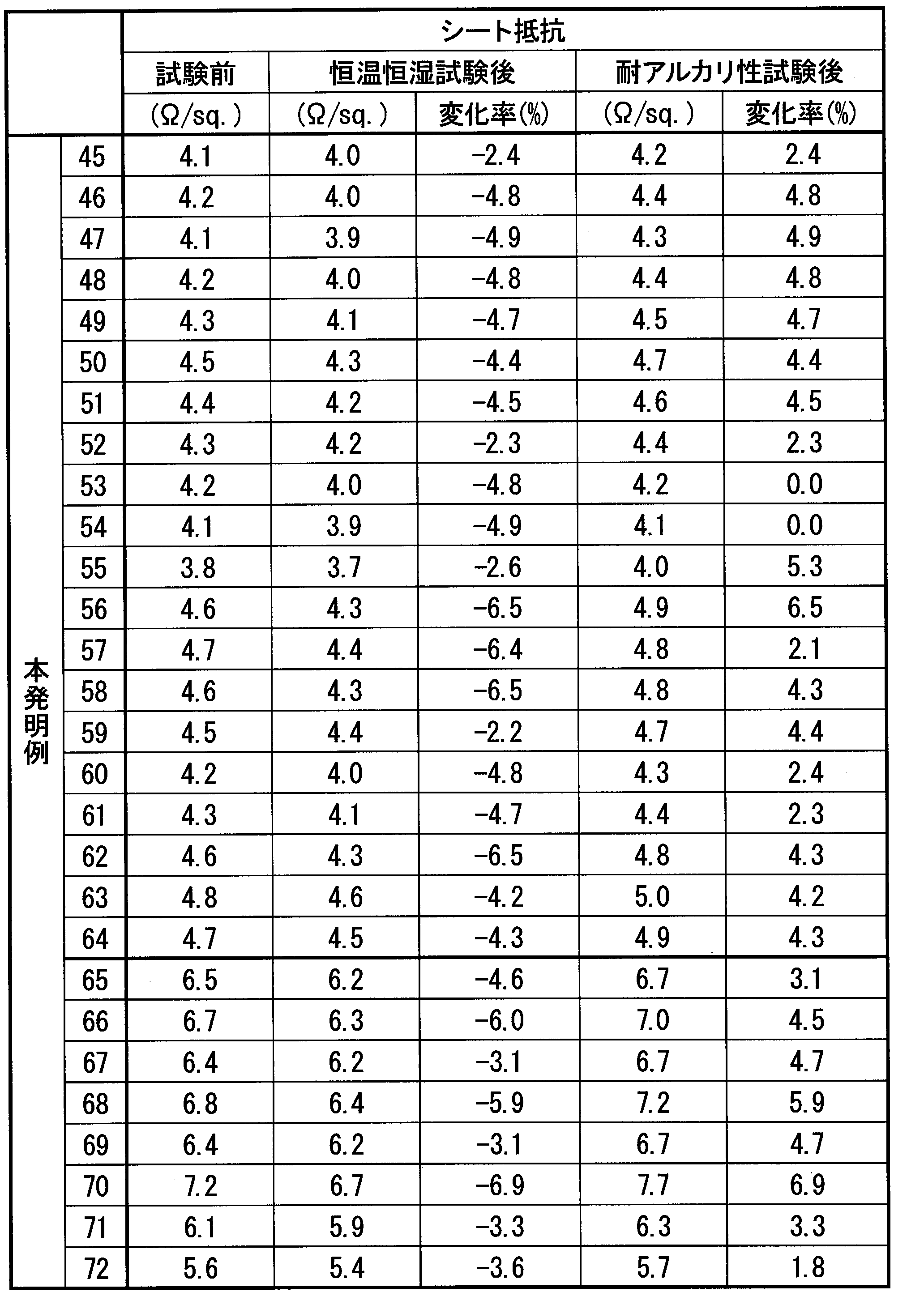
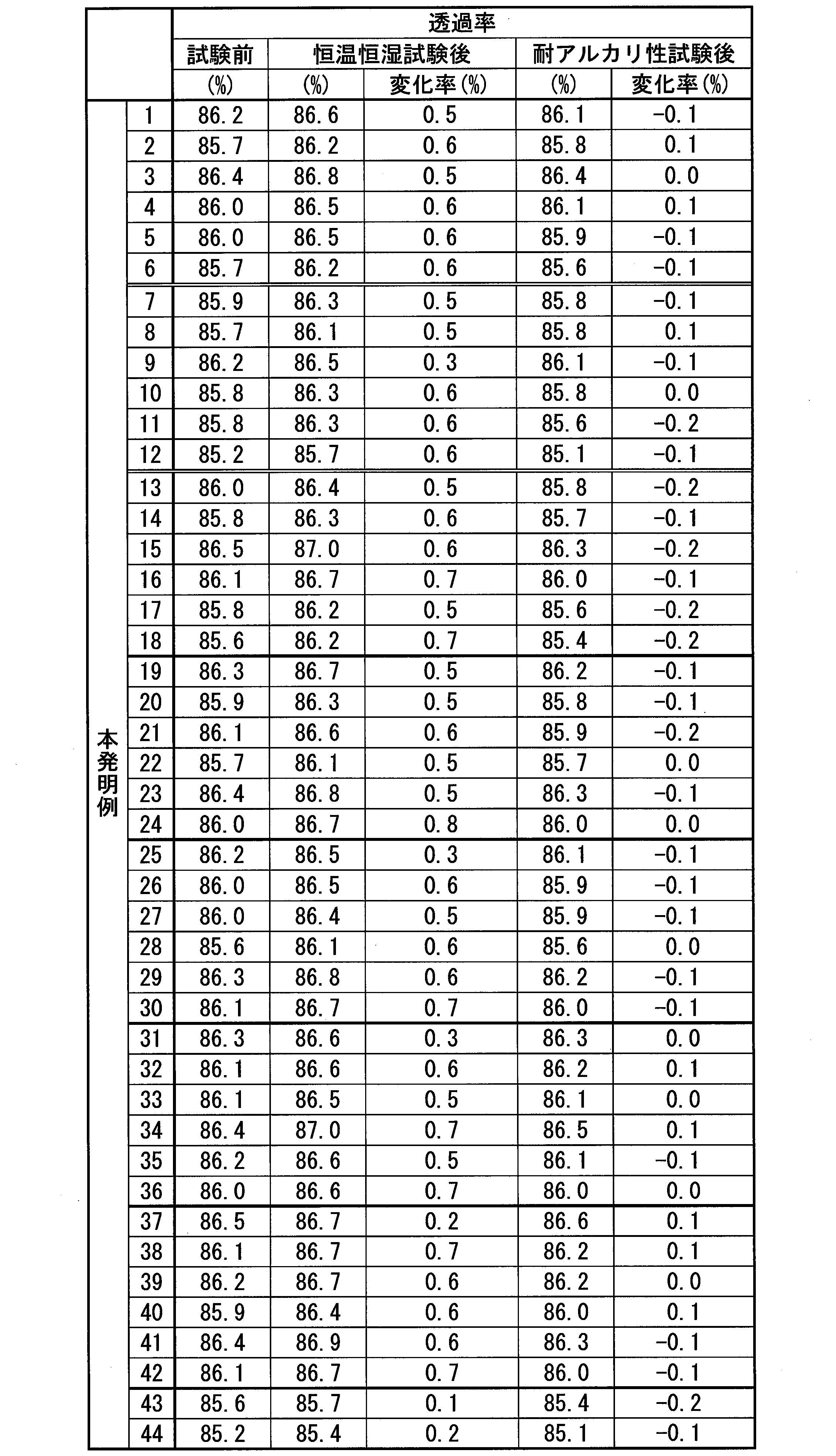


本発明例では、成膜後の平均透過率がいずれも85%を超えており、さらに、成膜後シート抵抗がいずれも10Ω/sq.以下であり、透過率に優れ、かつ、抵抗が十分に低い積層透明導電膜が得られることが確認された。
一方、比較例においては、成膜後の平均透過率がいずれも85%以下であり、成膜後のシート抵抗はAg膜の組成と膜厚が同じサンプルで比較すると本発明例に比べて高くなっていた。Ag膜においてAgの凝集が発生したためと推測される。
また、比較例Aでは、ITO単層膜を600nmと厚く形成することで、シート抵抗が10Ω/sq.以下となったが、平均透過率が76.4%と大きく劣化した。
さらに、比較例Bでは、ガラス基板を200℃に加熱することで、膜厚が180nmでシート抵抗が10Ω/sq.以下となったが、平均透過率は85%以下であった。
一方、比較例においては、成膜後の平均透過率がいずれも85%以下であり、成膜後のシート抵抗はAg膜の組成と膜厚が同じサンプルで比較すると本発明例に比べて高くなっていた。Ag膜においてAgの凝集が発生したためと推測される。
また、比較例Aでは、ITO単層膜を600nmと厚く形成することで、シート抵抗が10Ω/sq.以下となったが、平均透過率が76.4%と大きく劣化した。
さらに、比較例Bでは、ガラス基板を200℃に加熱することで、膜厚が180nmでシート抵抗が10Ω/sq.以下となったが、平均透過率は85%以下であった。
また、恒温恒湿試験の結果、本発明例では、恒温恒湿試験後の透過率及びシート抵抗の変化率が小さく、耐環境性に優れていることが確認された。
一方、比較例では、A、Bを除き、恒温恒湿試験後の透過率又はシート抵抗の変化率が大きく、耐環境性が不十分であった。
一方、比較例では、A、Bを除き、恒温恒湿試験後の透過率又はシート抵抗の変化率が大きく、耐環境性が不十分であった。
さらに、耐アルカリ性試験の結果、本発明例では、耐アルカリ性試験後の透過率及びシート抵抗の変化率が小さく、試験後の平均透過率は全て85%以上あり、耐アルカリ性に優れていることが確認された。
一方、比較例では、耐アルカリ性試験後の透過率又はシート抵抗の変化率が大きいサンプルが多く見られ、耐アルカリ性が不十分なサンプルが多かった。それらの変化率が小さいサンプルでも、試験後の平均透過率は全て85%以下であった。
一方、比較例では、耐アルカリ性試験後の透過率又はシート抵抗の変化率が大きいサンプルが多く見られ、耐アルカリ性が不十分なサンプルが多かった。それらの変化率が小さいサンプルでも、試験後の平均透過率は全て85%以下であった。
また、エッチング法によるパターンニング試験の結果、本発明例では、AgのオーバーエッチングOEや透明導電酸化物膜の残渣Rが認められず、配線パターンを精度良く形成可能であることが確認された。
一方、比較例では、AgのオーバーエッチングOEや透明導電酸化物膜の残渣Rが発生し、一括エッチングによっては、配線パターンを精度良く形成することが困難であった。
一方、比較例では、AgのオーバーエッチングOEや透明導電酸化物膜の残渣Rが発生し、一括エッチングによっては、配線パターンを精度良く形成することが困難であった。
また、リフトオフ法によるパターンニング試験の結果、本発明例において、配線パターンを精度良く形成可能であることが確認された。
以上のことから、本発明例によれば、Ag膜を薄く形成してもAgの凝集がなく、透過率が高く、抵抗値の低い積層透明導電膜を提供可能であることが確認された。
従来の透明導電膜よりも、可視光域の光の透過性がより高く、かつ電気抵抗のより低い透明導電膜を提供することができるようになる。その結果、より高品質なディスプレイあるいはタッチパネル等を提供することができるようになる。
10 積層透明導電膜
11 第1透明導電酸化物膜(透明導電酸化物膜)
12 Ag膜
13 第2透明導電酸化物膜(透明導電酸化物膜)
30 積層配線膜
41 レジスト膜
L ライン
S スペース
OE オーバーエッチング
R 残渣
11 第1透明導電酸化物膜(透明導電酸化物膜)
12 Ag膜
13 第2透明導電酸化物膜(透明導電酸化物膜)
30 積層配線膜
41 レジスト膜
L ライン
S スペース
OE オーバーエッチング
R 残渣
Claims (8)
- AgまたはAg合金よりなるAg膜と、前記Ag膜の両面に配置された透明導電酸化物膜と、を有し、
前記透明導電酸化物膜は、Zn、Ga、Y及びSnを含む酸化物からなることを特徴とする積層透明導電膜。 - 前記透明導電酸化物膜中に含まれる全金属元素の原子割合が、Ga;0.9原子%以上26.1原子%以下、Y;0.2原子%以上9.5原子%以下、Sn;0.1原子%以上4.7原子%以下、残Znとされていることを特徴とする請求項1に記載の積層透明導電膜。
- 前記Ag膜は、Cu、Sn、Sb、Ti、Mg、Zn、Ge、In、Al、Ga、Pd、Au、Pt、Bi、Mn、Sc、Y、Nd、Sm、Eu、Gd、Tb、Erのうちの1種又は2種以上を合計で0.2原子%以上10.0原子%以下含有し、残部がAg及び不可避不純物からなるAg合金で構成されていることを特徴とする請求項1または請求項2に記載の積層透明導電膜。
- 前記Ag膜の厚さが10nm以下とされていることを特徴とする請求項1から請求項3のいずれか一項に記載の積層透明導電膜。
- 波長400~800nmの可視光域の平均透過率が85%以上、シート抵抗値が10Ω/sq.以下であることを特徴とする請求項1から請求項4のいずれか一項に記載の積層透明導電膜。
- 請求項1から請求項5のいずれか一項に記載の積層透明導電膜からなり、配線パターンを有することを特徴とする積層配線膜。
- 請求項6に記載された積層配線膜の製造方法であって、
基材の成膜面に、前記Ag膜及び前記透明導電酸化物膜を含む前記積層透明導電膜を成膜する積層透明導電膜成膜工程と、
前記積層透明導電膜の上に配線パターン状のレジスト膜を形成するレジスト膜形成工程と、
前記レジスト膜が形成された前記積層透明導電膜に対して、リン酸、酢酸を含む酸性の混合液をエッチャントに用いて、エッチングを一括して行うエッチング工程と、
エッチング後に前記レジスト膜を除去するレジスト膜除去工程と、
を備えていることを特徴とする積層配線膜の製造方法。 - 請求項6に記載された積層配線膜の製造方法であって、
基材の成膜面に配線パターンの反転パターン状のレジスト膜を形成するレジスト膜形成工程と、
前記レジスト膜が形成された前記基材の成膜面に、前記Ag膜及び前記透明導電酸化物膜を含む前記積層透明導電膜を成膜する積層透明導電膜成膜工程と、
前記レジスト膜を除去するレジスト膜除去工程と、
を備えていることを特徴とする積層配線膜の製造方法。
Applications Claiming Priority (4)
| Application Number | Priority Date | Filing Date | Title |
|---|---|---|---|
| JP2016-014703 | 2016-01-28 | ||
| JP2016014703 | 2016-01-28 | ||
| JP2017003349A JP6870332B2 (ja) | 2016-01-28 | 2017-01-12 | 積層透明導電膜、積層配線膜及び積層配線膜の製造方法 |
| JP2017-003349 | 2017-01-12 |
Publications (1)
| Publication Number | Publication Date |
|---|---|
| WO2017131183A1 true WO2017131183A1 (ja) | 2017-08-03 |
Family
ID=59399099
Family Applications (1)
| Application Number | Title | Priority Date | Filing Date |
|---|---|---|---|
| PCT/JP2017/002998 Ceased WO2017131183A1 (ja) | 2016-01-28 | 2017-01-27 | 積層透明導電膜、積層配線膜及び積層配線膜の製造方法 |
Country Status (1)
| Country | Link |
|---|---|
| WO (1) | WO2017131183A1 (ja) |
Cited By (1)
| Publication number | Priority date | Publication date | Assignee | Title |
|---|---|---|---|---|
| CN113345644A (zh) * | 2021-06-07 | 2021-09-03 | 北方民族大学 | 一种柔性Ag/Zn导电薄膜及其制备方法和应用 |
Citations (3)
| Publication number | Priority date | Publication date | Assignee | Title |
|---|---|---|---|---|
| JP2011504639A (ja) * | 2007-11-22 | 2011-02-10 | サン−ゴバン グラス フランス | 電極を支持している基材、該基材を含む有機エレクトロルミネセントデバイス及びその製造 |
| JP2015228363A (ja) * | 2014-05-07 | 2015-12-17 | Tdk株式会社 | 積層型透明導電膜 |
| JP2016040411A (ja) * | 2014-08-12 | 2016-03-24 | 三菱マテリアル株式会社 | 積層膜、積層配線膜及び積層配線膜の製造方法 |
-
2017
- 2017-01-27 WO PCT/JP2017/002998 patent/WO2017131183A1/ja not_active Ceased
Patent Citations (3)
| Publication number | Priority date | Publication date | Assignee | Title |
|---|---|---|---|---|
| JP2011504639A (ja) * | 2007-11-22 | 2011-02-10 | サン−ゴバン グラス フランス | 電極を支持している基材、該基材を含む有機エレクトロルミネセントデバイス及びその製造 |
| JP2015228363A (ja) * | 2014-05-07 | 2015-12-17 | Tdk株式会社 | 積層型透明導電膜 |
| JP2016040411A (ja) * | 2014-08-12 | 2016-03-24 | 三菱マテリアル株式会社 | 積層膜、積層配線膜及び積層配線膜の製造方法 |
Cited By (1)
| Publication number | Priority date | Publication date | Assignee | Title |
|---|---|---|---|---|
| CN113345644A (zh) * | 2021-06-07 | 2021-09-03 | 北方民族大学 | 一种柔性Ag/Zn导电薄膜及其制备方法和应用 |
Similar Documents
| Publication | Publication Date | Title |
|---|---|---|
| JP6888318B2 (ja) | 積層透明導電膜、積層配線膜及び積層配線膜の製造方法 | |
| KR102327961B1 (ko) | 적층 반사 전극막, 적층 반사 전극 패턴, 적층 반사 전극 패턴의 제조 방법 | |
| WO2016024615A1 (ja) | 積層膜、積層配線膜及び積層配線膜の製造方法 | |
| KR101358529B1 (ko) | 전자부품용 적층 배선막 및 피복층 형성용 스퍼터링 타겟재 | |
| CN107735841A (zh) | 透明导电体 | |
| WO1998004406A1 (en) | Transparent conductive film and method for forming transparent electrode | |
| JP6870332B2 (ja) | 積層透明導電膜、積層配線膜及び積層配線膜の製造方法 | |
| JP5023745B2 (ja) | 透明導電膜、この透明導電膜を用いた透明導電性基板、透明導電性フィルム、並びに近赤外線遮断フィルター、および、この透明導電膜の製造方法 | |
| CN106796885B (zh) | 透明导电配线及透明导电配线的制造方法 | |
| KR101350648B1 (ko) | 전자부품용 적층 배선막 및 피복층 형성용 스퍼터링 타겟재 | |
| JP4971618B2 (ja) | 表示用電極パターン製造方法 | |
| WO2017131183A1 (ja) | 積層透明導電膜、積層配線膜及び積層配線膜の製造方法 | |
| WO2016111202A1 (ja) | 積層膜 | |
| JP6565666B2 (ja) | 積層透明導電膜、積層配線膜及び積層配線膜の製造方法 | |
| JP6597284B2 (ja) | 積層透明導電膜、積層配線膜及び積層配線膜の製造方法 | |
| JP2007163995A (ja) | 透明導電膜付き基板およびその製造方法 | |
| WO2017164209A1 (ja) | 積層透明導電膜、積層配線膜及び積層配線膜の製造方法 | |
| WO2017164211A1 (ja) | 積層反射電極膜、積層反射電極パターン、積層反射電極パターンの製造方法 | |
| WO2016136953A1 (ja) | 透明導電配線、及び、透明導電配線の製造方法 | |
| JP2016130010A (ja) | 積層膜 | |
| JP6123285B2 (ja) | 積層膜 | |
| JP2018087360A (ja) | 酸化物スパッタリングターゲット | |
| WO2021095550A1 (ja) | 積層構造体 |
Legal Events
| Date | Code | Title | Description |
|---|---|---|---|
| 121 | Ep: the epo has been informed by wipo that ep was designated in this application |
Ref document number: 17744413 Country of ref document: EP Kind code of ref document: A1 |
|
| NENP | Non-entry into the national phase |
Ref country code: DE |
|
| 122 | Ep: pct application non-entry in european phase |
Ref document number: 17744413 Country of ref document: EP Kind code of ref document: A1 |