WO2017122579A1 - 位相シフト方式フルブリッジ型電源回路 - Google Patents
位相シフト方式フルブリッジ型電源回路 Download PDFInfo
- Publication number
- WO2017122579A1 WO2017122579A1 PCT/JP2017/000190 JP2017000190W WO2017122579A1 WO 2017122579 A1 WO2017122579 A1 WO 2017122579A1 JP 2017000190 W JP2017000190 W JP 2017000190W WO 2017122579 A1 WO2017122579 A1 WO 2017122579A1
- Authority
- WO
- WIPO (PCT)
- Prior art keywords
- terminal
- circuit
- inductor
- switch element
- capacitor
- Prior art date
- Legal status (The legal status is an assumption and is not a legal conclusion. Google has not performed a legal analysis and makes no representation as to the accuracy of the status listed.)
- Ceased
Links
Images


Classifications
-
- H—ELECTRICITY
- H02—GENERATION; CONVERSION OR DISTRIBUTION OF ELECTRIC POWER
- H02M—APPARATUS FOR CONVERSION BETWEEN AC AND AC, BETWEEN AC AND DC, OR BETWEEN DC AND DC, AND FOR USE WITH MAINS OR SIMILAR POWER SUPPLY SYSTEMS; CONVERSION OF DC OR AC INPUT POWER INTO SURGE OUTPUT POWER; CONTROL OR REGULATION THEREOF
- H02M3/00—Conversion of DC power input into DC power output
- H02M3/22—Conversion of DC power input into DC power output with intermediate conversion into AC
- H02M3/24—Conversion of DC power input into DC power output with intermediate conversion into AC by static converters
- H02M3/28—Conversion of DC power input into DC power output with intermediate conversion into AC by static converters using discharge tubes with control electrode or semiconductor devices with control electrode to produce the intermediate AC
-
- H—ELECTRICITY
- H02—GENERATION; CONVERSION OR DISTRIBUTION OF ELECTRIC POWER
- H02M—APPARATUS FOR CONVERSION BETWEEN AC AND AC, BETWEEN AC AND DC, OR BETWEEN DC AND DC, AND FOR USE WITH MAINS OR SIMILAR POWER SUPPLY SYSTEMS; CONVERSION OF DC OR AC INPUT POWER INTO SURGE OUTPUT POWER; CONTROL OR REGULATION THEREOF
- H02M3/00—Conversion of DC power input into DC power output
- H02M3/22—Conversion of DC power input into DC power output with intermediate conversion into AC
- H02M3/24—Conversion of DC power input into DC power output with intermediate conversion into AC by static converters
- H02M3/28—Conversion of DC power input into DC power output with intermediate conversion into AC by static converters using discharge tubes with control electrode or semiconductor devices with control electrode to produce the intermediate AC
- H02M3/325—Conversion of DC power input into DC power output with intermediate conversion into AC by static converters using discharge tubes with control electrode or semiconductor devices with control electrode to produce the intermediate AC using devices of a triode or a transistor type requiring continuous application of a control signal
- H02M3/335—Conversion of DC power input into DC power output with intermediate conversion into AC by static converters using discharge tubes with control electrode or semiconductor devices with control electrode to produce the intermediate AC using devices of a triode or a transistor type requiring continuous application of a control signal using semiconductor devices only
Definitions
- the present invention relates to a phase shift type full bridge type power supply circuit.
- a return inductor has been added to the bridge circuit.
- Switching loss is suppressed.
- the switching loss of the switch element is suppressed by using the resonance characteristics of the LC resonance circuit composed of the return inductor and the capacitor of the bridge circuit (the parasitic capacitance of the switch element or the capacitor connected in parallel to the switch element). is doing.
- a phase shift type full bridge type power supply circuit capable of suppressing the loss of the transformer itself is known. See, for example, US Pat.
- the clamp diode can suppress the influence of the recovery surge voltage due to the return inductor to the rectifier diode of the rectifier circuit, but cannot suppress the recovery surge voltage due to the transformer leakage inductor. Since a transformer has a leakage inductor due to its structure, a recovery surge voltage is generated by the leakage inductor in the rectifier diode of the rectifier circuit. Therefore, conventionally, in order to suppress the recovery surge voltage, the rated voltage of the rectifier diode is increased in accordance with the recovery surge voltage. However, when the rated voltage of the rectifier diode is increased, the performance of the rectifier diode is degraded, and thus the recovery surge voltage is increased. In addition, the price of rectifier diodes will increase.
- An object according to one aspect of the present invention is to provide a phase shift type full bridge type power supply circuit that suppresses a recovery surge voltage due to a leakage inductor of a transformer.
- a phase shift type full bridge type power supply circuit includes a bridge circuit, a recovery surge protection circuit, a recovery surge suppression circuit, a transformer, and a rectifier circuit.
- the bridge circuit includes first to fourth switch elements connected in a full bridge type.
- the recovery surge protection circuit has first and second rectifying elements and is connected in parallel to the bridge circuit.
- one terminal of the inductor is connected to the anode terminal of the first rectifier element and the cathode terminal of the second rectifier element, and the other terminal of the inductor is one terminal of the third switch element.
- the fourth switch element is connected to one terminal of the fourth switch element, and a capacitor is connected in parallel to the inductor.
- the transformer has a primary winding and a secondary winding, and one terminal of the primary winding is connected to one terminal of the first switch element and one terminal of the second switch element. The other terminal of is connected to one terminal of the inductor.
- the rectifier circuit is connected to the secondary side of the transformer, and rectifies the AC voltage output from the transformer using the third and fourth rectifier elements.
- the control circuit controls driving and stopping of the first to fourth switch elements.
- the capacitor starts charging when the first and fourth switching elements are driven, and ends charging after the recovery of the fourth rectifying element, or the capacitor is driven when the second and third switching elements are driven. Charging is started, and charging ends after recovery of the third rectifying element occurs.
- FIG. 1 is a diagram showing an embodiment of a phase shift type full bridge type power supply circuit 1.
- the phase shift type full bridge type power supply circuit 1 includes a control circuit 2, an input capacitor C0, a bridge circuit, a recovery surge protection circuit 3 (clamp diode), a recovery surge suppression circuit 4, a transformer T, a rectifier circuit 5, and a smoothing circuit 6. ing.
- the phase shift type full bridge type power supply circuit 1 is, for example, a DC-DC converter that converts a DC input voltage Vin applied from a DC input power supply 7 into a DC output voltage Vout and drives a load 8.
- the control circuit 2 drives (ON: conduction) and stops (OFF: interruption) the switch elements Q1 to Q4 constituting the bridge circuit by control signals SQ1 to SQ4 output from a control terminal provided in the control circuit 2.
- the control circuit 2 includes, for example, a circuit configured using a CPU (Central Processing Unit), a multi-core CPU, a programmable device (FPGA (Field Programmable Gate Array), PLD (Programmable Logic Device), etc.), and a switching element Q1.
- CPU Central Processing Unit
- FPGA Field Programmable Gate Array
- PLD Programmable Logic Device
- the capacitor C0 is connected between the primary high voltage line HL1 connected to the positive terminal of the DC input power supply 7 and the primary low voltage line LL1 connected to the negative terminal of the DC input power supply 7.
- the bridge circuit has switch elements Q1 to Q4 (first to fourth switch elements) connected in a full bridge type.
- switch elements Q1 to Q4 MOSFETs (Metal / Oxide / Semiconductor / Field / Effect / Transistor), IGBTs (Insulated / Gate / Bipolor / Transistor), or the like may be used.
- MOSFETs Metal / Oxide / Semiconductor / Field / Effect / Transistor
- IGBTs Insulated / Gate / Bipolor / Transistor
- drain terminal (the other terminal) of the switch element Q1 and the drain terminal (the other terminal) of the switch element Q3 are connected, and the source terminal (the other terminal) of the switch element Q2 and the source terminal of the switch element Q4 (the other terminal) Terminal).
- capacitor C1 and the diode D1 are connected in parallel to the switch element Q1
- the capacitor C2 and the diode D2 are connected in parallel to the switch element Q2
- the capacitor C3 and the diode D3 are connected in parallel to the switch element Q3, and the switch element Q4
- a capacitor C4 and a diode D4 are connected in parallel.
- parasitic capacitors of the switch elements Q1 to Q4 may be used for the capacitors C1 to C4
- parasitic diodes of the switch elements Q1 to Q4 may be used for the diodes D1 to D4.
- gate terminals of the switch elements Q1 to Q4 are connected to the control terminal of the control circuit 2, and the switch elements Q1 to Q4 are controlled by the control signals SQ1 to SQ4 output from the control terminal.
- the recovery surge protection circuit 3 includes diodes D5 and D6 (first and second rectifying elements).
- the recovery surge protection circuit 3 is generated in the diodes D7 and D8 (third and fourth rectifier elements) of the rectifier circuit 5 connected to the secondary side of the transformer T by adding the inductor La (reflux inductor). Suppresses recovery surge voltage.
- the cathode terminal of the diode D5 is connected to the primary high-voltage line HL1, the drain terminal of the switch element Q1, and the drain terminal of the switch element Q3, the anode terminal of the diode D5 and the cathode terminal of the diode D6 are connected, and the anode of the diode D6
- the terminals are connected to the primary low-voltage line LL1, the source terminal of the switch element Q2, and the source terminal of the switch element Q4.
- one terminal of the inductor La is connected to the anode terminal of the diode D5 and the cathode terminal of the diode D6, and the other terminal of the inductor La is the source terminal of the switch element Q3 and the drain of the switch element Q4.
- the capacitor Ca is connected in parallel to the inductor La.
- the inductor La is an inductor provided to realize the ZVS of the switch elements Q1 to Q4, and configures an LC resonance circuit together with the capacitors C1 to C4 to use the resonance characteristics, thereby switching loss of the switch elements Q1 to Q4. Suppress.
- the circuit in which the capacitor Ca is connected in parallel to the inductor La is a circuit that suppresses the recovery surge voltage generated in the diodes D7 and D8 of the rectifier circuit 5 connected to the secondary side of the transformer T by the leakage inductor L1 of the transformer T. It is. That is, the current I L flowing through the inductor La, and diode D7, current flows through the primary winding 9 of the transformer T to D8 recovery upon occurrence of I T (load current + recovery current), a by causing charged in the capacitor Ca, trans
- This circuit reduces the input voltage (2 ⁇ Vin / N) applied to the secondary windings 10a and 10b of T and suppresses the recovery surge voltage generated by the leakage inductor L1 of the transformer T.
- N is a turn ratio of the primary winding 9 and the secondary windings 10a and 10b of the transformer T, and is N: 1: 1.
- the transformer T has a primary winding 9 and secondary windings 10a and 10b.
- One terminal of the primary winding 9 is connected to the source terminal of the switch element Q1 and the drain terminal of the switch element Q2, and the other terminal of the primary winding 9 is connected to one terminal of the inductor La.
- One terminal of each of the secondary windings 10a and 10b is connected to each other at a midpoint (center tap).
- the rectifier circuit 5 is connected to the secondary side of the transformer T, and rectifies and outputs the AC voltage output from the transformer T using the diodes D7 and D8.
- the other terminal of the secondary winding 10a is connected to the cathode terminal of the diode D7
- the other terminal of the secondary winding 10b is connected to the cathode terminal of the diode D8, and the middle point is one of the inductors L0 of the smoothing circuit 6.
- the anode terminals of the diodes D7 and D8 are connected to the secondary low voltage line LL2.
- the diodes D7 and D8 may be MOSFETs. However, when a MOSFET is used, it is preferable to drive the MOSFET itself in synchronization with a period during which the parasitic diode of the MOSFET is conductive.
- the smoothing circuit 6 has an inductor L0 and a capacitor C5.
- the smoothing circuit 6 smoothes the voltage rectified by the rectifying circuit 5 and outputs a DC output voltage Vout.
- power is supplied to the load 8.
- the other terminal of the inductor L0 is connected to one terminal of the capacitor C5 and the secondary high voltage line HL2, and the other terminal of the capacitor C5 is connected to the secondary low voltage line LL2.
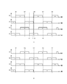
- FIG. 2A is a diagram showing the switching timing (driving (on) and stopping) when the switching elements Q1 and Q2 are in the leading phase.
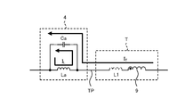
- FIG. 3 is a diagram showing a current flow of the recovery surge suppression circuit 4.
- the recovery surge voltage of the diode D8 has a form in which the resonance voltage due to the parasitic capacitance of the leakage inductor L1 and the diode D8 is superimposed around the voltage 2 ⁇ Vin / N applied to the secondary windings 10a and 10b of the transformer T. . Therefore, when there is no capacitor Ca as in the conventional phase shift type full bridge type power supply circuit, a recovery surge voltage exceeding the rated voltage of the diode D8 is applied as shown in FIGS.
- FIG. 4 is a diagram illustrating a waveform when a recovery surge of the diode D8 of the rectifier circuit 5 occurs.
- the voltage V T2 of the secondary windings 10a and 10b of the transformer T is 2 ⁇ Vin even if the switch elements Q1 and Q4 are driven at the time ta shown in FIGS. Not lower than / N. Therefore, when the recovery surge occurrence time t1 of the diode D8 is reached, the recovery surge voltage is superimposed around the voltage 2 ⁇ Vin / N and exceeds the rated voltage of the diode D8.
- the capacitor Ca starts charging when the switch elements Q1 and Q4 are driven and the recovery surge voltage of the diode D8 is terminated after the recovery surge is generated, thereby suppressing the recovery surge voltage.
- the elements Q2 and Q3 are driven. That is, when the switch elements Q2 and Q3 are driven at t4 in FIG. 2, the capacitor Ca can suppress the recovery surge voltage by starting charging and ending charging after the recovery surge of the diode D7 occurs. .
- the capacitor Ca starts charging, the voltage at the measurement point TP in FIG. 1 approaches 0 [V] from the DC input voltage Vin, contrary to E in FIG.
- FIG. 2 is a diagram illustrating switching timing (driving (on) and stopping) when the switching elements Q1 and Q2 are in a delayed phase.
- the rated voltage of the diodes D7 and D8 can be lowered by suppressing the recovery surge voltage, the forward voltage (on-time voltage drop) can be reduced and the loss can be reduced. In addition, the prices of the diodes D7 and D8 are reduced.
Landscapes
- Engineering & Computer Science (AREA)
- Power Engineering (AREA)
- Dc-Dc Converters (AREA)
Abstract
ブリッジ回路と、ブリッジ回路に並列接続されるリカバリーサージ保護回路3と、インダクタLaの一方の端子が第1の整流素子D5のアノードと第2の整流素子D6のカソードと接続され、インダクタの他方の端子が第3のスイッチ素子Q3の一方の端子と第4のスイッチ素子Q4の一方の端子と接続され、インダクタにキャパシタCaが並列接続されるリカバリーサージ抑制回路4と、第3、第4の整流素子D7、D8を有する整流回路5と、を備え、キャパシタは、第1、第4のスイッチ素子Q1、Q4が駆動すると充電し、第4の整流素子のリカバリーサージ発生より後に充電が終了し、あるいは、第2、第3のスイッチ素子Q2、Q3が駆動すると充電し、第3の整流素子のリカバリーサージ発生より後に充電が終了する。
Description
本発明は、位相シフト方式フルブリッジ型電源回路に関する。
従来、位相シフト方式フルブリッジ型電源回路において、トランスの一次側に接続されるブリッジ回路のスイッチ素子のZVS(Zero Voltage Switching)を実現するために、ブリッジ回路に還流インダクタを追加してスイッチ素子のスイッチング損失を抑制している。すなわち、還流インダクタと、ブリッジ回路のキャパシタ(スイッチ素子の寄生容量又はスイッチ素子に並列接続されているキャパシタ)と、により構成されるLC共振回路の共振特性を利用し、スイッチ素子のスイッチング損失を抑制している。例えば、関連する技術として、トランス自身の損失を抑えることが可能な位相シフト方式フルブリッジ型電源回路が知られている。例えば、特許文献1を参照。
ところが、還流インダクタをブリッジ回路に追加すると、トランスの二次側に接続される整流回路の整流ダイオードのリカバリーサージ電圧が大きくなる。そこでトランスの一次側にクランプダイオードを設けてリカバリーサージ電圧を抑制している。
しかしながら、クランプダイオードは、整流回路の整流ダイオードへの還流インダクタによるリカバリーサージ電圧の影響を抑制できるが、トランスの漏れインダクタによるリカバリーサージ電圧を抑制することはできない。トランスには構造上どうしても漏れインダクタが存在するため、整流回路の整流ダイオードにはこの漏れインダクタによるリカバリーサージ電圧が発生する。そこで、従来はこのリカバリーサージ電圧を抑制するため、リカバリーサージ電圧に応じて、整流ダイオードの定格電圧を大きくして対応していた。ところが、整流ダイオードの定格電圧を大きくすると、整流ダイオードの性能低下につながるため、リカバリーサージ電圧が大きくなってしまうことになる。更に整流ダイオードの価格上昇にもつながる。
本発明の一側面に係る目的は、トランスの漏れインダクタによるリカバリーサージ電圧を抑制する位相シフト方式フルブリッジ型電源回路を提供することである。
本発明に係る一つの形態である位相シフト方式フルブリッジ型電源回路は、ブリッジ回路、リカバリーサージ保護回路、リカバリーサージ抑制回路、トランス、整流回路を備える。
ブリッジ回路は、フルブリッジ型に接続される第1~第4のスイッチ素子を有する。
リカバリーサージ保護回路は、第1、第2の整流素子を有し、ブリッジ回路に並列接続される。
リカバリーサージ保護回路は、第1、第2の整流素子を有し、ブリッジ回路に並列接続される。
リカバリーサージ抑制回路は、インダクタの一方の端子が、第1の整流素子のアノード端子と第2の整流素子のカソード端子と接続され、インダクタの他方の端子が、第3のスイッチ素子の一方の端子と第4のスイッチ素子の一方の端子と接続され、インダクタにキャパシタが並列接続される。
トランスは、一次巻線と二次巻線を有し、一次巻線の一方の端子は、第1のスイッチ素子の一方の端子と第2のスイッチ素子の一方の端子と接続され、一次巻線の他方の端子は、インダクタの一方の端子と接続される。
整流回路は、トランスの二次側に接続され、第3、第4の整流素子を用いてトランスから出力される交流電圧を整流する。
制御回路は、第1~第4のスイッチ素子の駆動と停止を制御する。
制御回路は、第1~第4のスイッチ素子の駆動と停止を制御する。
キャパシタは、第1、第4のスイッチ素子が駆動すると充電を開始し、第4の整流素子のリカバリー発生より後に充電を終了し、あるいは、キャパシタは、第2、第3のスイッチ素子が駆動すると充電を開始し、第3の整流素子のリカバリー発生より後に充電が終了する。
トランスの漏れインダクタによるリカバリーサージ電圧を抑制することができる。
以下図面に基づいて実施形態について詳細を説明する。
図1は、位相シフト方式フルブリッジ型電源回路1の一実施例を示す図である。位相シフト方式フルブリッジ型電源回路1は、制御回路2、入力キャパシタC0、ブリッジ回路、リカバリーサージ保護回路3(クランプダイオード)、リカバリーサージ抑制回路4、トランスT、整流回路5、平滑回路6を備えている。位相シフト方式フルブリッジ型電源回路1は、例えば、直流入力電源7から印加される直流入力電圧Vinを直流出力電圧Voutに変換して負荷8を駆動するDC-DCコンバータなどである。
図1は、位相シフト方式フルブリッジ型電源回路1の一実施例を示す図である。位相シフト方式フルブリッジ型電源回路1は、制御回路2、入力キャパシタC0、ブリッジ回路、リカバリーサージ保護回路3(クランプダイオード)、リカバリーサージ抑制回路4、トランスT、整流回路5、平滑回路6を備えている。位相シフト方式フルブリッジ型電源回路1は、例えば、直流入力電源7から印加される直流入力電圧Vinを直流出力電圧Voutに変換して負荷8を駆動するDC-DCコンバータなどである。
制御回路2は、ブリッジ回路を構成するスイッチ素子Q1~Q4の駆動(オン:導通)と停止(オフ:遮断)を、制御回路2に設けられている制御端子から出力する制御信号SQ1~SQ4により制御する。制御回路2は、例えば、CPU(Central Processing Unit)、マルチコアCPU、プログラマブルなデバイス(FPGA(Field Programmable Gate Array)やPLD(Programmable Logic Device)など)などを用いて構成される回路と、スイッチ素子Q1~Q4を駆動させる駆動回路などから構成される。
キャパシタC0は、直流入力電源7の正極端子に接続される一次側高圧線HL1と、直流入力電源7の負極端子に接続される一次側低圧線LL1と、の間に接続されている。
ブリッジ回路は、フルブリッジ型に接続されるスイッチ素子Q1~Q4(第1~第4のスイッチ素子)を有する。スイッチ素子Q1~Q4は、MOSFET(Metal Oxide Semiconductor Field Effect Transistor)やIGBT(Insulated Gate Bipolor Transistor)などを用いることが考えられる。図1の例では、スイッチ素子Q1のソース端子(一方の端子)とスイッチ素子Q2のドレイン端子(一方の端子)とが接続され、スイッチ素子Q3のソース端子(一方の端子)とスイッチ素子Q4のドレイン端子(一方の端子)とが接続されている。また、スイッチ素子Q1のドレイン端子(他方の端子)とスイッチ素子Q3のドレイン端子(他方の端子)とが接続され、スイッチ素子Q2のソース端子(他方の端子)とスイッチ素子Q4のソース端子(他方の端子)とが接続されている。
また、スイッチ素子Q1にはキャパシタC1及びダイオードD1が並列接続され、スイッチ素子Q2にはキャパシタC2及びダイオードD2が並列接続され、スイッチ素子Q3にはキャパシタC3及びダイオードD3が並列接続され、スイッチ素子Q4にはキャパシタC4及びダイオードD4が並列接続されている。ただし、キャパシタC1~C4にはスイッチ素子Q1~Q4の寄生容量を用いてもよいし、ダイオードD1~D4にはスイッチ素子Q1~Q4の寄生ダイオードを用いてもよい。
なお、スイッチ素子Q1~Q4のゲート端子は制御回路2の制御端子と接続され、制御端子から出力される制御信号SQ1~SQ4によりスイッチ素子Q1~Q4が制御される。
リカバリーサージ保護回路3は、ダイオードD5、D6(第1、第2の整流素子)を有する。リカバリーサージ保護回路3は、インダクタLa(還流インダクタ)を追加したことにより、トランスTの二次側に接続される整流回路5のダイオードD7、D8(第3、第4の整流素子)に発生するリカバリーサージ電圧を抑制する。ダイオードD5のカソード端子は一次側高圧線HL1とスイッチ素子Q1のドレイン端子とスイッチ素子Q3のドレイン端子とが接続され、ダイオードD5のアノード端子とダイオードD6のカソード端子とが接続され、ダイオードD6のアノード端子は一次側低圧線LL1とスイッチ素子Q2のソース端子とスイッチ素子Q4のソース端子とが接続されている。
リカバリーサージ抑制回路4は、インダクタLaの一方の端子が、ダイオードD5のアノード端子とダイオードD6のカソード端子と接続され、インダクタLaの他方の端子が、スイッチ素子Q3のソース端子とスイッチ素子Q4のドレイン端子と接続され、インダクタLaにキャパシタCaが並列接続されている。
インダクタLaは、スイッチ素子Q1~Q4のZVSを実現するために設けられたインダクタで、キャパシタC1~C4とともにLC共振回路を構成して共振特性を利用することで、スイッチ素子Q1~Q4のスイッチング損失を抑制する。
また、インダクタLaにキャパシタCaを並列接続した回路は、トランスTの漏れインダクタL1により、トランスTの二次側に接続される整流回路5のダイオードD7、D8に発生するリカバリーサージ電圧を抑制する回路である。すなわち、インダクタLaに流れる電流ILと、ダイオードD7、D8のリカバリー発生時にトランスTの一次巻線9に流れる電流IT(負荷電流+リカバリー電流)と、をキャパシタCaに充電させることで、トランスTの二次巻線10a、10bへ印加される入力電圧(2×Vin/N)を下げ、トランスTの漏れインダクタL1により発生するリカバリーサージ電圧を抑制する回路である。NはトランスTの一次巻線9と二次巻線10a、10bの巻数比で、N:1:1となる。
トランスTは、一次巻線9と二次巻線10a、10bとを有している。一次巻線9の一方の端子は、スイッチ素子Q1のソース端子とスイッチ素子Q2のドレイン端子とに接続され、一次巻線9の他方の端子は、インダクタLaの一方の端子と接続される。二次巻線10a、10bそれぞれの一方の端子は中点(センタータップ)で互いに接続されている。
整流回路5は、トランスTの二次側に接続され、ダイオードD7、D8を用いてトランスTから出力される交流電圧を整流して出力する。二次巻線10aの他方の端子はダイオードD7のカソード端子に接続され、二次巻線10bの他方の端子はダイオードD8のカソード端子に接続され、中点は、平滑回路6のインダクタL0の一方の端子に接続されている。ダイオードD7、D8それぞれのアノード端子は二次側低圧線LL2に接続されている。なお、ダイオードD7、D8はMOSFETを用いてもよい。ただし、MOSFETを用いた場合、MOSFETの寄生ダイオードが導通する期間と同期して、MOSFET自身を駆動することが好ましい。
平滑回路6は、インダクタL0、キャパシタC5を有する。平滑回路6は、整流回路5で整流された電圧を平滑化して直流出力電圧Voutを出力する。図1の例では負荷8に給電している。なお、インダクタL0の他方の端子はキャパシタC5の一方の端子と二次側高圧線HL2に接続され、キャパシタC5の他方の端子は二次側低圧線LL2に接続される。
位相シフト方式フルブリッジ型電源回路1の動作を説明する。
図2のAは、スイッチ素子Q1、Q2が進み相とした場合のスイッチングタイミング(駆動(on)と停止)を示す図である。
図2のAは、スイッチ素子Q1、Q2が進み相とした場合のスイッチングタイミング(駆動(on)と停止)を示す図である。
図2のt1において、スイッチ素子Q4が駆動(ターンオン:on)し、スイッチ素子Q2、Q4がともに駆動(オン:on)すると、漏れインダクタL1→スイッチ素子Q2→スイッチ素子Q4→インダクタLa→漏れインダクタL1の経路で電流が流れ漏れインダクタL1のエネルギーは還流する。
続いて、図2のt2において、スイッチ素子Q2が停止(ターンオフ)して、スイッチ素子Q4のみが駆動(オン:on)になると、キャパシタC2が充電され、キャパシタC1が放電される。そして、キャパシタC2の充電とキャパシタC1の放電が完了すると、漏れインダクタL1→ダイオードD1→直流入力電源7→スイッチ素子Q4→インダクタLa→漏れインダクタL1の経路で電流が流れる。
ダイオードD1が導通している時間に、図2のt3において、スイッチ素子Q1が駆動(ターンオン:on)し、スイッチ素子Q1、Q4がともに駆動すると、漏れインダクタL1→スイッチ素子Q1→直流入力電源7→スイッチ素子Q4→キャパシタCa→漏れインダクタL1の経路で電流ITが流れる。このときにキャパシタCaは充電を開始する。なお、時間t0における電流ILと電流ITと電流Ioとの関係は(式1)のように表せる。
Io/N>IT=IL (式1)
次に、漏れインダクタL1が直流入力電圧Vinで逆方向に印加されると、漏れインダクタL1のエネルギーが減少し、電流ITの向きが反転し、直流入力電源7→スイッチ素子Q1→漏れインダクタL1→キャパシタCa→スイッチ素子Q4→直流入力電源7の経路で電流ITが流れる。
次に、漏れインダクタL1が直流入力電圧Vinで逆方向に印加されると、漏れインダクタL1のエネルギーが減少し、電流ITの向きが反転し、直流入力電源7→スイッチ素子Q1→漏れインダクタL1→キャパシタCa→スイッチ素子Q4→直流入力電源7の経路で電流ITが流れる。
ダイオードD8のリカバリーサージ発生時にもキャパシタCaの充電は継続され、図3に示すようにインダクタLaに流れる電流IL、及び、ダイオードD8のリカバリーサージ発生時にトランスTの一次巻線9に流れる電流IT(負荷電流+リカバリーサージ電流)は、キャパシタCaに充電されているので、トランスTの二次巻線10a、10bに印加される入力電圧が下がる。図3は、リカバリーサージ抑制回路4の電流の流れを示す図である。
続いて、ダイオードD8のリカバリーサージ発生時間を経過すると、キャパシタCaの充電を終了する。その後、キャパシタCaの充電が終了すると、キャパシタCaの放電が開始され、二次巻線10a、10bの両端の電圧は2×Vin/Nに戻る。このとき電流ILと電流ITと電流Ioとの関係は(式2)のように表せる。
Io/N=IT<IL (式2)
このように、ダイオードD8のリカバリーサージ発生時にキャパシタCaに電流ILと電流ITを充電させることで、トランスTの二次巻線10a、10bに印加される入力電圧を下げ、トランスTの漏れインダクタL1により発生するリカバリーサージ電圧を下げる。
このように、ダイオードD8のリカバリーサージ発生時にキャパシタCaに電流ILと電流ITを充電させることで、トランスTの二次巻線10a、10bに印加される入力電圧を下げ、トランスTの漏れインダクタL1により発生するリカバリーサージ電圧を下げる。
ダイオードD8のリカバリーサージ電圧は、トランスTの二次巻線10a、10bに印加される電圧2×Vin/Nを中心に、漏れインダクタL1、ダイオードD8の寄生容量による共振電圧が重畳した形になる。従って、従来の位相シフト方式フルブリッジ型電源回路のようにキャパシタCaがない場合、図4のA、Bに示すように、ダイオードD8の定格電圧を超えたリカバリーサージ電圧が印加されてしまう。図4は、整流回路5のダイオードD8のリカバリーサージ発生時の波形を示す図である。
キャパシタCaがない場合、図2、図4のA、Bに示した時間taにおいてスイッチ素子Q1、Q4が駆動しても、トランスTの二次巻線10a、10bの電圧VT2は2×Vin/Nより低下しない。そのためダイオードD8のリカバリーサージ発生時間t1になると、電圧2×Vin/Nを中心にしてリカバリーサージ電圧が重畳され、ダイオードD8の定格電圧を超えてしまう。
キャパシタCaがある場合、キャパシタCaへの充電は、図2、図4のC~Fに示した時間taにおいてスイッチ素子Q1、Q4が駆動すると開始され、ダイオードD8のリカバリーサージ発生時間tbより後で終了するように設定されているので、キャパシタCaが充電を開始すると図4のEに示すように図1の計測点TPの電圧は0[V]から直流入力電圧Vinに近づき、一次巻線9の両端の電圧が下がり、それにともない二次巻線10a、10bの電圧も下がる。また、トランスTの二次巻線10a、10bの電圧は、リカバリーサージ電圧がダイオードD8の定格電圧を超えない電圧まで下げる。
また、以上では、スイッチ素子Q1、Q4が駆動すると、キャパシタCaが充電を開始し、ダイオードD8のリカバリーサージ発生より後に充電を終了することで、リカバリーサージ電圧を抑制する場合について説明したが、スイッチ素子Q2、Q3が駆動した場合にも同様のことが言える。すなわち、キャパシタCaは、図2のt4において、スイッチ素子Q2、Q3が駆動すると、充電を開始してダイオードD7のリカバリーサージ発生より後に充電を終了することで、リカバリーサージ電圧を抑制することができる。なお、キャパシタCaが充電を開始すると図4のEとは逆に図1の計測点TPの電圧は直流入力電圧Vinから0[V]に近づく。
また、以上では、スイッチ素子Q1、Q2が進み相の場合について説明をしたが、図2のBに示すようにスイッチ素子Q1、Q2が遅れ相の場合にも、以上で説明したリカバリーサージ電圧を抑制する方法を適用することができる。図2のBは、スイッチ素子Q1、Q2が遅れ相とした場合のスイッチングタイミング(駆動(on)と停止)を示す図である。
更に、リカバリーサージ電圧を抑制することで、ダイオードD7、D8の定格電圧を下げることができるので、順方向電圧(オン時電圧ドロップ)を小さくでき、損失も低減させることができる。また、ダイオードD7、D8の価格を下げることにつながる。
また、本発明は、以上の実施の形態に限定されるものでなく、本発明の要旨を逸脱しない範囲内で種々の改良、変更が可能である。
1 位相シフト方式フルブリッジ型電源回路
2 制御回路
3 リカバリーサージ保護回路
4 リカバリーサージ抑制回路
5 整流回路
6 平滑回路
7 直流入力電源
8 負荷
9 一次巻線
10a、10b 二次巻線
C0、C1、C2、C3、C4、C5、Ca キャパシタ
D1、D2、D3、D4、D5、D6、D7、D8 ダイオード
L0、La インダクタ
L1 漏れインダクタ
Q1、Q2、Q3、Q4 スイッチ素子
T トランス
2 制御回路
3 リカバリーサージ保護回路
4 リカバリーサージ抑制回路
5 整流回路
6 平滑回路
7 直流入力電源
8 負荷
9 一次巻線
10a、10b 二次巻線
C0、C1、C2、C3、C4、C5、Ca キャパシタ
D1、D2、D3、D4、D5、D6、D7、D8 ダイオード
L0、La インダクタ
L1 漏れインダクタ
Q1、Q2、Q3、Q4 スイッチ素子
T トランス
Claims (2)
- フルブリッジ型に接続される第1~第4のスイッチ素子を有するブリッジ回路と、
第1、第2の整流素子を有し、前記ブリッジ回路に並列接続されるリカバリーサージ保護回路と、
インダクタの一方の端子は、前記第1の整流素子のアノード端子と前記第2の整流素子のカソード端子と接続され、前記インダクタの他方の端子は、前記第3のスイッチ素子の一方の端子と前記第4のスイッチ素子の一方の端子と接続され、前記インダクタにキャパシタが並列接続されるリカバリーサージ抑制回路と、
一次巻線と二次巻線を有し、前記一次巻線の一方の端子は、前記第1のスイッチ素子の一方の端子と前記第2のスイッチ素子の一方の端子と接続され、前記一次巻線の他方の端子は、前記インダクタの一方の端子と接続されるトランスと、
前記トランスの二次側に接続され、第3、第4の整流素子を用いて前記トランスから出力される交流電圧を整流する整流回路と、
前記第1~第4のスイッチ素子の駆動と停止を制御する制御回路と、
を備えることを特徴とする位相シフト方式フルブリッジ型電源回路。 - 請求項1に記載の位相シフト方式フルブリッジ型電源回路であって、
前記キャパシタは、前記第1、第4のスイッチ素子が駆動すると充電を開始し、前記第4の整流素子のリカバリーサージ発生より後に充電が終了し、あるいは、前記キャパシタは、前記第2、第3のスイッチ素子が駆動すると充電を開始し、前記第3の整流素子のリカバリーサージ発生より後に充電が終了する、
ことを特徴とする位相シフト方式フルブリッジ型電源回路。
Applications Claiming Priority (2)
| Application Number | Priority Date | Filing Date | Title |
|---|---|---|---|
| JP2016-003374 | 2016-01-12 | ||
| JP2016003374A JP6485366B2 (ja) | 2016-01-12 | 2016-01-12 | 位相シフト方式フルブリッジ型電源回路 |
Publications (1)
| Publication Number | Publication Date |
|---|---|
| WO2017122579A1 true WO2017122579A1 (ja) | 2017-07-20 |
Family
ID=59312047
Family Applications (1)
| Application Number | Title | Priority Date | Filing Date |
|---|---|---|---|
| PCT/JP2017/000190 Ceased WO2017122579A1 (ja) | 2016-01-12 | 2017-01-06 | 位相シフト方式フルブリッジ型電源回路 |
Country Status (2)
| Country | Link |
|---|---|
| JP (1) | JP6485366B2 (ja) |
| WO (1) | WO2017122579A1 (ja) |
Families Citing this family (2)
| Publication number | Priority date | Publication date | Assignee | Title |
|---|---|---|---|---|
| US11239745B2 (en) * | 2018-04-11 | 2022-02-01 | Aerojet Rocketdyne, Inc | Power converter including a recirculating snubber |
| JP7230738B2 (ja) | 2019-08-09 | 2023-03-01 | 株式会社オートネットワーク技術研究所 | 複合部品 |
Citations (3)
| Publication number | Priority date | Publication date | Assignee | Title |
|---|---|---|---|---|
| WO2007000830A1 (ja) * | 2005-06-29 | 2007-01-04 | Murata Manufacturing Co., Ltd. | Dc-dcコンバータ |
| JP2008187801A (ja) * | 2007-01-29 | 2008-08-14 | Tdk Corp | スイッチング電源装置 |
| WO2015118631A1 (ja) * | 2014-02-05 | 2015-08-13 | 三菱電機株式会社 | 車載充電器、車載充電器におけるサージ抑制方法 |
-
2016
- 2016-01-12 JP JP2016003374A patent/JP6485366B2/ja active Active
-
2017
- 2017-01-06 WO PCT/JP2017/000190 patent/WO2017122579A1/ja not_active Ceased
Patent Citations (3)
| Publication number | Priority date | Publication date | Assignee | Title |
|---|---|---|---|---|
| WO2007000830A1 (ja) * | 2005-06-29 | 2007-01-04 | Murata Manufacturing Co., Ltd. | Dc-dcコンバータ |
| JP2008187801A (ja) * | 2007-01-29 | 2008-08-14 | Tdk Corp | スイッチング電源装置 |
| WO2015118631A1 (ja) * | 2014-02-05 | 2015-08-13 | 三菱電機株式会社 | 車載充電器、車載充電器におけるサージ抑制方法 |
Also Published As
| Publication number | Publication date |
|---|---|
| JP6485366B2 (ja) | 2019-03-20 |
| JP2017127051A (ja) | 2017-07-20 |
Similar Documents
| Publication | Publication Date | Title |
|---|---|---|
| US9190911B2 (en) | Auxiliary resonant apparatus for LLC converters | |
| US9124190B2 (en) | Isolated switched mode power supply | |
| US9350260B2 (en) | Startup method and system for resonant converters | |
| US20150124487A1 (en) | Adjustable Resonant Apparatus for Power Converters | |
| JP6241334B2 (ja) | 電流共振型dcdcコンバータ | |
| CN105684287A (zh) | 用于谐振转换器的栅驱动装置 | |
| JP5644125B2 (ja) | 直流−直流変換回路の起動方法 | |
| US8064228B2 (en) | Power supply apparatus with current-sharing function | |
| JP2014143911A (ja) | コンバーター | |
| US9564819B2 (en) | Switching power supply circuit | |
| US6999325B2 (en) | Current/voltage converter arrangement | |
| JP2015042080A (ja) | スイッチング電源装置 | |
| US9748851B2 (en) | Switching power supply apparatus with snubber circuit | |
| JP4410599B2 (ja) | スイッチング電源装置 | |
| US9263959B2 (en) | Forward converter with self-driven BJT synchronous rectifier | |
| JP4110477B2 (ja) | Dc−dcコンバータ | |
| KR20160101808A (ko) | 풀브리지 dc-dc 컨버터 | |
| JP5516055B2 (ja) | 電力変換装置 | |
| KR20150070898A (ko) | 직류-직류 컨버터 및 이의 스위칭 방법 | |
| JP6458235B2 (ja) | スイッチング電源装置 | |
| JP6485366B2 (ja) | 位相シフト方式フルブリッジ型電源回路 | |
| US11356029B2 (en) | Rectifying circuit and switched-mode power supply incorporating rectifying circuit | |
| JP6129687B2 (ja) | スイッチング電源装置 | |
| JPH1118426A (ja) | スイッチング電源回路 | |
| JP2006191706A (ja) | 直流変換装置 |
Legal Events
| Date | Code | Title | Description |
|---|---|---|---|
| 121 | Ep: the epo has been informed by wipo that ep was designated in this application |
Ref document number: 17738334 Country of ref document: EP Kind code of ref document: A1 |
|
| NENP | Non-entry into the national phase |
Ref country code: DE |
|
| 122 | Ep: pct application non-entry in european phase |
Ref document number: 17738334 Country of ref document: EP Kind code of ref document: A1 |