WO2017110571A1 - Device with built-in component, rfid tag, and method for producing device with built-in component - Google Patents
Device with built-in component, rfid tag, and method for producing device with built-in component Download PDFInfo
- Publication number
- WO2017110571A1 WO2017110571A1 PCT/JP2016/086968 JP2016086968W WO2017110571A1 WO 2017110571 A1 WO2017110571 A1 WO 2017110571A1 JP 2016086968 W JP2016086968 W JP 2016086968W WO 2017110571 A1 WO2017110571 A1 WO 2017110571A1
- Authority
- WO
- WIPO (PCT)
- Prior art keywords
- chip
- thermoplastic resin
- input
- rfid
- laminate
- Prior art date
Links
Images


Classifications
-
- G—PHYSICS
- G06—COMPUTING; CALCULATING OR COUNTING
- G06K—GRAPHICAL DATA READING; PRESENTATION OF DATA; RECORD CARRIERS; HANDLING RECORD CARRIERS
- G06K19/00—Record carriers for use with machines and with at least a part designed to carry digital markings
- G06K19/02—Record carriers for use with machines and with at least a part designed to carry digital markings characterised by the selection of materials, e.g. to avoid wear during transport through the machine
-
- G—PHYSICS
- G06—COMPUTING; CALCULATING OR COUNTING
- G06K—GRAPHICAL DATA READING; PRESENTATION OF DATA; RECORD CARRIERS; HANDLING RECORD CARRIERS
- G06K19/00—Record carriers for use with machines and with at least a part designed to carry digital markings
- G06K19/06—Record carriers for use with machines and with at least a part designed to carry digital markings characterised by the kind of the digital marking, e.g. shape, nature, code
- G06K19/067—Record carriers with conductive marks, printed circuits or semiconductor circuit elements, e.g. credit or identity cards also with resonating or responding marks without active components
- G06K19/07—Record carriers with conductive marks, printed circuits or semiconductor circuit elements, e.g. credit or identity cards also with resonating or responding marks without active components with integrated circuit chips
- G06K19/077—Constructional details, e.g. mounting of circuits in the carrier
-
- H—ELECTRICITY
- H01—ELECTRIC ELEMENTS
- H01Q—ANTENNAS, i.e. RADIO AERIALS
- H01Q9/00—Electrically-short antennas having dimensions not more than twice the operating wavelength and consisting of conductive active radiating elements
- H01Q9/04—Resonant antennas
- H01Q9/16—Resonant antennas with feed intermediate between the extremities of the antenna, e.g. centre-fed dipole
-
- H—ELECTRICITY
- H04—ELECTRIC COMMUNICATION TECHNIQUE
- H04B—TRANSMISSION
- H04B1/00—Details of transmission systems, not covered by a single one of groups H04B3/00 - H04B13/00; Details of transmission systems not characterised by the medium used for transmission
- H04B1/38—Transceivers, i.e. devices in which transmitter and receiver form a structural unit and in which at least one part is used for functions of transmitting and receiving
- H04B1/40—Circuits
-
- H—ELECTRICITY
- H05—ELECTRIC TECHNIQUES NOT OTHERWISE PROVIDED FOR
- H05K—PRINTED CIRCUITS; CASINGS OR CONSTRUCTIONAL DETAILS OF ELECTRIC APPARATUS; MANUFACTURE OF ASSEMBLAGES OF ELECTRICAL COMPONENTS
- H05K3/00—Apparatus or processes for manufacturing printed circuits
- H05K3/46—Manufacturing multilayer circuits
Definitions
- the present invention relates to a component built-in device in which a chip-shaped electronic component is built in a laminate of resin layers, an RFID tag including the device, and a method for manufacturing the component built-in device.
- An RFID tag used for article information management includes an RFID IC chip that holds predetermined information and processes predetermined radio signals, and an antenna element that transmits and receives high-frequency signals, and is a management target. Used by being applied to various articles and their packaging materials.
- an HF band RFID system using a 13.56 MHz band and a UHF band RFID system using a 900 MHz band are generally used.
- the UHF band RFID system is characterized in that the communication distance is relatively long and a plurality of tags can be collectively read.
- a UHF band RFID tag a tag having a structure disclosed in Patent Document 1 is known.
- the RFID tag disclosed in Patent Document 1 includes a printed wiring board on which a radiating element is formed and an electromagnetic coupling module including an RFIC.
- the electromagnetic coupling module includes a power supply circuit board made of, for example, a ceramic substrate and a semiconductor RFIC chip.
- An external terminal is provided on the lower surface of the power supply circuit board, the RFIC chip is mounted on the upper surface, and the power supply is performed so as to cover the RFIC chip.
- a protective film is coated on the upper surface of the circuit board.
- a module similar to the above module can be electrically configured. Since a module using a laminate of resin sheets is easily thinned and flexible, it is suitable for an RFID tag that is thin and requires flexibility.
- FIGS. FIG. 15A is a cross-sectional view of the main part of the RFID module
- FIG. 15B is a partially enlarged view thereof.
- Each resin sheet has a predetermined conductor pattern, and when a plurality of resin sheets are laminated together, the pad electrode is deformed (resin flow during pressing) particularly in the vicinity of the hard IC chip 50. 21a and 21b are deformed.
- the above-mentioned problems are not limited to RFID modules, but are common to all component-embedded devices having a structure in which chip-shaped electronic components are embedded in a laminate of thermoplastic resin layers.
- An object of the present invention is a component-embedded device having a structure in which a chip-shaped electronic component is embedded in a laminate of thermoplastic resin layers, wherein the structure and electrical connection around the chip-shaped electronic component in the laminate are stabilized
- An object is to provide a built-in device, an RFID tag including the same, and a method for manufacturing a component built-in device.
- the component built-in device of the present invention is A component built-in device comprising a laminate of a plurality of thermoplastic resin layers, and a chip-like electronic component embedded in the laminate,
- the chip-shaped electronic component has input / output terminals,
- pad electrodes formed on a thermoplastic resin layer different from the layer where the input / output terminals of the chip-like electronic component are located, and
- a plurality of first interlayer connection conductors for conducting the input / output terminal and the pad electrode in an interlayer direction are provided.
- the chip-shaped electronic component has a rectangular parallelepiped shape, and the input / output terminals are arranged along two parallel sides of the bottom surface of the chip-shaped electronic component,
- the pad electrode has a shape extending along the two sides,
- the plurality of first interlayer connection conductors are preferably arranged at symmetrical positions with respect to the longitudinal center of the input / output terminal along the two sides. Thereby, the inclination of the pad electrode is relaxed, and the structure and electrical connection around the chip-shaped electronic component in the stacked body are stabilized.
- the component built-in device of the present invention is A component built-in device comprising a laminate of a plurality of thermoplastic resin layers, and a chip-like electronic component embedded in the laminate,
- the chip-shaped electronic component has input / output terminals,
- pad electrodes formed on a thermoplastic resin layer different from the layer where the input / output terminals of the chip-like electronic component are located, and
- a first interlayer connection conductor having a long axis and a cross-sectional shape on a surface along the thermoplastic resin layer, which conducts the input / output terminal and the pad electrode in an interlayer direction, is provided. .
- the chip electronic component is a rectangular parallelepiped
- the input / output terminals are arranged along two mutually parallel sides of the bottom surface of the chip electronic component
- the pad electrode is the two sides
- the first interlayer connecting conductor is disposed along the two sides.
- the first interlayer connection conductor is disposed at a symmetrical position with respect to the center in the longitudinal direction of the input / output terminal along the two sides. Thereby, the stress applied to the pad electrode is easily balanced, and the tilt of the chip-shaped electronic component is suppressed.
- the pad electrode has a larger area than the input / output terminal, and the chip-like electronic component in plan view from the lamination direction of the thermoplastic resin layer. It is preferable to have a region that does not overlap. Thereby, it can apply to the chip-shaped electronic components of various sizes, without changing each thermoplastic resin layer (sheet
- the laminate includes a conductor pattern along an in-plane direction of the thermoplastic resin layer and a second interlayer connection conductor that conducts to the conductor pattern, It is preferable that an element is constituted by the conductor pattern and the second interlayer connection conductor, and a diameter of the plurality of first interlayer connection conductors is smaller than a diameter of the second interlayer connection conductor. Thereby, a buffering property is generated between the chip-shaped electronic component and the pad electrode, and the stress concentration on the pad electrode is further relaxed. Further, the present invention can be applied to a chip-shaped electronic component having a smaller input / output terminal.
- the RFID tag of the present invention is A flexible insulator substrate having a radiating element with a conductor pattern, and an RFID module having an external terminal, wherein the RFID module is mounted on the insulator substrate, and the external terminal is connected to the radiating element.
- the RFID module is Comprising a laminate of a plurality of thermoplastic resin layers, a coiled conductor pattern made of a conductor formed in the thermoplastic resin layer, and an RFID IC embedded in the laminate, The RFID IC has an input / output terminal, The laminate includes a pad electrode that is electrically connected to an input / output terminal of the RFID IC and the external terminal.
- the RFID IC and the coiled conductor pattern are connected by joining the input / output terminal and the pad electrode,
- the pad electrode is formed in a thermoplastic resin layer different from a layer in which the input / output terminal of the RFID IC is located among the plurality of thermoplastic resin layers,
- the input / output terminal and the pad electrode are electrically connected in the interlayer direction by a plurality of first interlayer connection conductors.
- the laminate has a longitudinal direction
- the coiled conductor pattern includes a first coiled conductor pattern and a second coiled conductor pattern
- the first coiled conductor pattern is disposed near the first end in the longitudinal direction.
- the second coiled conductor pattern is disposed near the second end in the longitudinal direction
- the RFID IC is arranged in plan view from the lamination direction of the thermoplastic resin layer and the first coiled conductor pattern and the first coiled conductor pattern. It is preferable to arrange between two coil-shaped conductor patterns. Thereby, it can reduce in size and the unnecessary coupling
- a method for manufacturing a component-embedded device is a method for manufacturing a component-embedded device comprising a laminate of a plurality of thermoplastic resin layers and a chip-like electronic component embedded in the laminate, Forming a pad electrode to which an input / output terminal of the chip-shaped electronic component is connected to the predetermined thermoplastic resin sheet among the plurality of thermoplastic resin sheets; and Forming a plurality of interlayer connection conductor forming holes for connecting the input / output terminals and the pad electrodes at a plurality of locations among the plurality of thermoplastic resin sheets, and filling the holes with a conductive paste; and A step of laminating and pressing the plurality of thermoplastic resin sheets together with the chip-shaped electronic component to form a laminate; and It is characterized by providing.
- a component built-in device in which the structure and electrical connection around the chip-shaped electronic component in the multilayer body is stabilized can be obtained.
- the present invention it is possible to obtain a component built-in device and an RFID tag including the same, in which the structure and electrical connection around the chip-shaped electronic component in the laminate are stabilized.
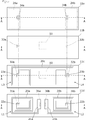
- FIG. 1 is a perspective view of an RFID module 101 according to the first embodiment.
- FIG. 2 is a bottom view showing an example of a thermoplastic resin sheet and various conductor patterns formed in the RFID module 101.
- FIG. 3A is a cross-sectional view of the RFID module 101 taken along the line AA in FIG.
- FIG. 3B is a plan view of the RFID IC chip 50 as viewed from the input / output terminal side.
- FIG. 4 is a circuit diagram of the RFID module 101.
- FIG. 5 is a bottom view showing an example of a resin sheet and various conductor patterns formed on the RFID module constituting the RFID module according to the second embodiment.
- FIG. 6 is a bottom view showing an example of a resin sheet and various conductor patterns formed on them, which constitute another RFID module according to the second embodiment.
- FIG. 7 is a plan view showing an example of a thermoplastic resin sheet and various conductor patterns formed on the thermoplastic resin sheet constituting the RFID module 103 according to the third embodiment.
- FIG. 8A is a cross-sectional view of the RFID module 103 taken along the line AA in FIG.
- FIG. 8B is a partially enlarged cross-sectional view showing the structure of the connection portion from the input / output terminal of the RFID IC chip 50 to the end electrodes 25a and 25b.
- FIG. 9 is a perspective view of an RFID tag 203 according to the fourth embodiment.
- FIG. 10 is a cross-sectional view showing the structure of the connection portion of the RFID module 101 with respect to the antenna substrate 91.
- FIG. 11 is a circuit diagram illustrating the operation of the RFID module 101 in the RFID tag 203.
- FIG. 12A is a perspective view of an RFID tag 204A according to the fifth embodiment.
- FIG. 12B is a perspective view showing the shape of the radiation elements 81a and 81b with the RFID module 101 separated.
- FIG. 13 is a perspective view of another RFID tag 204B according to the fifth embodiment.
- FIG. 14 is a perspective view of still another RFID tag 204C according to the fifth embodiment.
- FIG. 15A is a cross-sectional view of the main part of the RFID module when an IC chip is simply embedded in a laminate of thermoplastic resin layers, and FIG. 15B is a partially enlarged view thereof.
- FIG. 1 is a perspective view of an RFID module 101 according to the first embodiment.
- the RFID module 101 of this embodiment is typically an RFID module corresponding to a communication frequency in the 900 MHz band, that is, the UHF band, and includes a rectangular parallelepiped laminated body 11.
- the laminate 11 is obtained by laminating a heat-flexible resin layer such as a liquid crystal polymer or polyimide, and the laminate 11 itself also exhibits flexibility.
- the dielectric constant of each insulating layer made of these materials is smaller than the dielectric constant of a ceramic base layer represented by LTCC.
- External terminals 24a and 24b are formed on the mounting surface (upper surface from the viewpoint in FIG. 1) of the laminate 11.
- the RFID module 101 is mounted on an antenna substrate described later. By this mounting, the external terminals 24a and 24b are connected to the radiating elements on the antenna substrate.
- FIG. 2 is a bottom view showing an example of a thermoplastic resin sheet and various conductor patterns formed on the thermoplastic resin sheet constituting the RFID module 101 (a view of each thermoplastic resin sheet looking up from the bottom surface).
- thermoplastic resin sheet (hereinafter simply referred to as “resin sheet”) 11d, rectangular spiral element patterns 20a and 20b are formed, respectively.
- a pad electrode 21a is formed at the first end of the element pattern 20a, and an end electrode 22a is formed at the second end.
- a pad electrode 21b is formed at the first end of the element pattern 20b, and an end electrode 22b is formed at the second end.
- the pad electrodes 21a and 21b have shapes extending from the end portions of the element patterns 20a and 20b along the two sides where the input / output terminals of the RFID IC chip 50 are formed.
- An element pattern 20c having two rectangular spiral portions is formed on the resin sheet 11c. End electrodes 23a and 23b are formed on both ends of the element pattern 20c. External terminals 24a and 24b are formed on the resin sheet 11a.
- Another resin sheet exists on the outer surface of the resin sheet 11d.
- the end electrode 22a of the element pattern 20a and the end electrode 23a of the element pattern 20c are connected via a via conductor 31a.
- the end electrode 22b of the element pattern 20b and the end electrode 23b of the element pattern 20c are connected through a via conductor 31b.
- the end electrodes 23a, 23b of the element pattern 20c and the external terminals 24a, 24b are connected via via conductors 32a, 32b, 33a, 33b, 34a, 34b.
- FIG. 3A is a cross-sectional view of the RFID module 101 taken along the line AA in FIG.
- the left rectangular spiral portion of the element pattern 20c and the element pattern 20a overlap in a substantially coaxial relationship.
- the rectangular spiral portion on the right side of the element pattern 20c and the element pattern 20b overlap in a substantially coaxial relationship.
- the end electrode 23a is connected to the external terminal 24a via the via conductors 32a, 33a, 34a.
- the end electrode 23b is connected to the external terminal 24b via the via conductors 32b, 33b, and 34b.
- a left coil spiral portion of the element pattern 20c and the element pattern 20a constitute a first coil-shaped conductor pattern, and a right rectangular spiral portion of the element pattern 20c and the element pattern 20b are second.
- a coiled conductor pattern is formed.
- FIG. 3B is a bottom view of the RFID IC chip 50 as viewed from the input / output terminal side.
- the RFID IC chip 50 has a rectangular parallelepiped shape, and the input / output terminals 50Ea and 50Eb are arranged along two parallel sides of the bottom surface of the RFID IC chip 50.
- the via conductors 35a1 and 35a2 are disposed at symmetrical positions with respect to the center in the longitudinal direction along the input / output terminals 50Ea and 50Eb along the two sides.
- a one-dot chain line in FIG. 3B indicates a central line in the longitudinal direction.
- the input / output terminal 50Ea of the IC chip for RFID 50 is connected to the pad electrode 21a via the via conductors 35a1 and 35a2.
- the input / output terminal 50Eb is connected to the pad electrode 21b via the via conductors 35b1 and 35b2.
- the via conductors 35a1, 35a2, 35b1, and 35b2 are provided near the end portions of the pad electrodes 21a and 21b.
- the via conductors 35a1, 35a2, 35b1, and 35b2 are examples of the “first interlayer connection conductor” according to the present invention.
- the diameter of the via conductors 35a1, 35a2, 35b1, and 35b2 is, for example, not less than 40 ⁇ m and not more than 90 ⁇ m, and preferably not less than 60 ⁇ m and not more than 70 ⁇ m.
- the via conductors 31a, 32a, 33a, 34a, 31b, 32b, 33b, and 34b are examples of the “second interlayer connection conductor” according to the present invention.
- the diameters of the via conductors 31a, 32a, 33a, 34a, 31b, 32b, 33b, and 34b are, for example, 60 ⁇ m or more and 140 ⁇ m or less, preferably 90 ⁇ m or more and 110 ⁇ m or less.
- the laminate 11 has a longitudinal direction, the first coiled conductor pattern is disposed near the first end in the longitudinal direction, and the second coiled conductor pattern is disposed near the second end in the longitudinal direction,
- the RFID IC 50 is disposed between the first coiled conductor pattern and the second coiled conductor pattern in a plan view from the lamination direction of the thermoplastic resin layer. Thereby, the RFID module 101 can be reduced in size, and unnecessary coupling between the coil formed by the first coiled conductor pattern and the coil formed by the second coiled conductor pattern is suppressed.
- FIG. 4 is a circuit diagram of the RFID module 101.
- the inductors L1 and L2 correspond to the element patterns 20a and 20b
- the inductors L3 and L4 correspond to the element pattern 20c.
- a plurality of (two in this embodiment) via conductors 35a1 and 35a2 are provided between the input / output terminals 50Ea and 50Eb of the RFID IC chip 50 and the pad electrodes 21a and 21b. , 35b1 and 35b2 are interposed.
- the deformation of the pad electrode due to the stress concentration on the pad electrodes 21a and 21b is alleviated, and the pad electrodes 21a and 21b are prevented from contacting the edge of the RFID IC chip 50.
- the end portions of the pad electrode 21a are pressed by the via conductors 35a1 and 35a2 and the end portions of the pad electrode 21b are pressed by the via conductors 35b1 and 35b2, the deformation of the pad electrodes 21a and 21b is effectively suppressed.
- the pad electrodes 21a and 21b have a larger area than the input / output terminals 50Ea and 50Eb, and have regions that do not overlap with the RFID IC chip 50 in plan view from the lamination direction of the thermoplastic resin layer. As described above, problems due to the deformation of the pad electrodes 21a and 21b are avoided, so that various sizes of IC chips for RFID 50 can be embedded. That is, even when RFID IC chips having different sizes are used, a single type of laminate 11 can be used.
- the first via conductors (via conductors 35a1, 35a2, 35b1, 35b2 that connect the input / output terminals 50Ea, 50Eb of the RFID IC chip 50 and the pad electrodes 21a, 21b) are second via conductors (element pattern 20a).
- 20b and the element pattern 20c are interlayer-connected via conductors 31a and 31b, and the end conductors 23a and 23b and the external terminals 24a and 24b are interlayer-connected via conductors 34a and 34b). Therefore, a buffering property is generated between the RFID IC chip 50 and the pad electrodes 21a and 21b, and stress concentration on the pad electrodes 21a and 21b is further alleviated.
- the present invention can be applied to a chip-shaped electronic component having smaller input / output terminals 50Ea and 50Eb.
- the pad electrodes 21a and 21b and the input / output terminals 50Ea and 50Eb of the RFID IC chip 50 are connected via a plurality of via conductors, respectively, the surface of the RFID IC chip 50 with respect to the pad electrodes 21a and 21b is increased. High tolerance for buried position shift. In other words, even if there is a positional deviation in the surface direction of the RFID IC chip 50 with respect to the pad electrodes 21a and 21b, electrical conduction is ensured because the conduction is made through one or more via conductors.
- the manufacturing method of the RFID module 101 of the present embodiment is as follows.
- thermoplastic resin sheet with a Cu foil attached on one side is prepared, and the Cu foil is patterned by photolithography to form predetermined conductor patterns on the thermoplastic resin sheets 11a to 11e, respectively. That is, the element patterns 20a and 20b and the pad electrodes 21a and 21b are formed on the thermoplastic resin sheet 11e. An element pattern 20c is formed on the thermoplastic resin sheet 11d. External terminals 24a and 24b are formed on the thermoplastic resin sheet 11a. The other thermoplastic resin sheet is formed with an electrode in contact with the via conductor.
- thermoplastic resin sheets 11a to 11e are laminated together with the RFID IC chip 50, and the laminate 11 is formed by applying pressure and heating.
- the second embodiment shows several examples in which the shape of the first via is different from that of the first embodiment.
- FIG. 5 is a bottom view (a view of each thermoplastic resin sheet looking up from the bottom surface) showing an example of a resin sheet and various conductor patterns formed in the RFID module according to the second embodiment.
- via conductors 36a and 36b are provided to connect the input / output terminals of the RFID IC chip 50 to the pad electrodes 21a and 21b.
- the via conductor 36a is composed of a plurality of via conductors. That is, via conductors adjacent to each other are connected. Similarly, the via conductors 36b are connected to adjacent via conductors.
- Laser processing is used to irradiate a predetermined position of a thermoplastic resin sheet with a laser beam many times to continuously form adjacent holes, and the conductive paste is filled therewith, so that via conductors adjacent to each other are formed.
- a via conductor having a continuous shape is formed.
- Other configurations are the same as those shown in the first embodiment.
- FIG. 6 is a bottom view showing an example of a resin sheet and various conductor patterns formed on them, which constitute another RFID module according to the second embodiment.
- via conductors 37a and 37b are provided to connect the input / output terminals of the RFID IC chip 50 to the pad electrodes 21a and 21b.
- These via conductors 37a and 37b have an oval cross-sectional shape and a long axis. That is, when a via hole is formed at a predetermined position of a thermoplastic resin sheet by a laser processing method, an oblong hole is formed by irradiating a laser beam substantially continuously and filled with a conductive paste. As a result, a via conductor having an oval cross-sectional shape is formed.
- Other configurations are the same as those shown in the first embodiment.
- stress concentration on the pad electrode is further relaxed, and local deformation of the pad electrode is avoided, so that the pad electrode can be prevented from contacting the edge of the chip-shaped electronic component.
- the plurality of first vias are arranged in a row in the longitudinal direction of the input / output terminals, but they may be arranged in a plurality of rows.
- FIG. 7 is a plan view showing an example of a thermoplastic resin sheet and various conductor patterns formed on the thermoplastic resin sheet constituting the RFID module 103 according to the third embodiment.
- FIG. 8A is a cross-sectional view of the RFID module 103 taken along the line AA in FIG.
- FIG. 8B is a partial enlarged cross-sectional view showing the structure of the connection portion from the input / output terminals 50Ea, 50Eb to the end electrodes 25a, 25b of the RFID IC chip 50.
- Resin sheet 11e is formed with rectangular spiral element patterns 20a and 20b, respectively.
- a pad electrode 25a is formed at the first end of the element pattern 20a, and an end electrode 22a is formed at the second end.
- a pad electrode 25b is formed at the first end of the element pattern 20b, and an end electrode 22b is formed at the second end.
- the pad electrodes 25a and 25b have shapes extending from the end portions of the element patterns 20a and 20b along the two sides where the input / output terminals of the RFID IC chip 50 are formed.
- An element pattern 20c having two rectangular spiral portions is formed on the resin sheet 11d. End electrodes 23a and 23b are formed on both ends of the element pattern 20c. Further, pad electrodes 21a and 21b are formed on the resin sheet 11d. External terminals 24a and 24b are formed on the resin sheet 11a. Another resin sheet exists between the resin sheet 11a and the resin sheet 11c.
- the RFID IC chip 50 has input / output terminals 50Ea and 50Eb arranged at positions along two opposing sides of the bottom surface of the RFID IC chip 50.
- the input / output terminals 50Ea and 50Eb are connected to the pad electrodes 21a and 21b via via conductors 35a1, 35a2, 35b1 and 35b2.
- the pad electrode connection conductors 45a and 45b connect the pad electrodes 21a and 21b and the end electrodes 25a and 25b.
- the regions where the via conductors 35a1, 35a2, 35b1, and 35b2 are present in the plan view from the lamination direction of the fat layer sheets 11a to 11e are represented by the first regions Z1a and Z1b.
- Regions where 45a and 45b exist are represented by second regions Z2a and Z2b.
- the second regions Z2a and Z2b are closer to the center of the RFID IC chip 50 than the first regions Z1a and Z1b.
- the pad electrodes 21a and 21b may come into contact with the edges of the RFID IC chip 50 (locations indicated by P in FIG. 8B) due to the deformation. Can be avoided. Since the regions other than the input / output terminals 50Ea and 50Eb are covered with the insulator film 50P on the surfaces where the input / output terminals 50Ea and 50Eb of the RFID IC chip 50 are formed, the pad electrodes 21a and 21b are formed with via conductors 45a and 45b. The pad electrodes 21a and 21b are not electrically connected to the substrate of the RFID IC chip 50 even if they are pressed against the surface where the input / output terminals 50Ea and 50Eb of the RFID IC chip 50 are formed by the pressing force.
- the RFID tag of this embodiment is applied to, for example, a tag for linen management, a label tag for clothes used for uniform management, and various name tags.
- FIG. 9 is a perspective view of the RFID tag 203 according to the fourth embodiment.
- the RFID tag 203 includes an antenna base 91 on which radiating elements 81a and 81b with conductor patterns are formed, and an RFID module 101.
- the configuration of the RFID module 101 is as shown in the first embodiment.
- Radiating elements 81a and 81b constitute a dipole antenna.
- the antenna substrate 91 is a resin sheet having flexibility such as PET.
- the radiating elements 81a and 81b are flexible conductors such as aluminum foil or copper foil.
- FIG. 10 is a cross-sectional view showing the structure of the connection portion of the RFID module 101 with respect to the antenna substrate 91.
- External terminals 24a and 24b of the RFID module 101 are connected to the radiating elements 81a and 81b via solders 38a and 38b.
- the formation region of the external terminals 24a and 24b and the embedded region of the RFID IC chip 50 are rigid regions, and the rest are flexible regions. Therefore, even if the RFID tag 203 is curved, the antenna base 91 and the RFID module 101 are bent as shown in FIG. 10, and a large bending stress is not applied to the RFID IC chip 50.
- FIG. 11 is a circuit diagram showing the operation of the RFID module 101 in the RFID tag 203.
- a capacitance Cp in the RFID IC chip 50 exists between the external terminals 24 a and 24 b, and two resonances occur in the RFID tag 203.
- the first resonance is a resonance that occurs in the current path indicated by the current i1, which is composed of the radiation elements 81a and 81b and the inductors L3 and L4, and the second resonance is composed of the inductors L1 to L4 and the capacitor Cp. This is resonance that occurs in the current path (current loop) indicated by current i2.
- the two resonances are coupled by inductors L3 to L4 shared by the respective current paths.
- Both the resonance frequency due to the first resonance and the resonance frequency due to the second resonance are affected by the inductors L3 to L4.
- a difference of several tens of MHz (specifically, about 5 to 50 MHz) is caused between the resonance frequency due to the first resonance and the resonance frequency due to the second resonance.
- FIG. 12A is a perspective view of an RFID tag 204A according to the fifth embodiment.
- FIG. 12B is a perspective view showing the shape of the radiation elements 81a and 81b with the RFID module 101 separated.
- a rectangular through hole HL2 is provided at the center in the length direction of the radiation elements 82a and 82b, and a notch CT1 reaching the through hole HL2 from the outer edge is further provided. In this way, a matching conductor pattern may be formed at the mounting position of the RFID module.
- FIG. 13 is a perspective view of another RFID tag 204B according to the fifth embodiment.
- the antenna base 92 is formed with a rectangular loop-shaped radiating element 83 which is partially opened, and an external terminal of the RFID module 101 is connected to the open portion.
- FIG. 14 is a perspective view of still another RFID tag 204C according to the fifth embodiment.
- the antenna base 92 is formed with a rectangular loop-shaped radiating element 84 having a through hole HL2 and a notch CT1 similar to the radiating element shown in FIG. 12B, and RFID is provided at both ends of the notch CT1.
- An external terminal of the module 101 is connected.
- a matching conductor pattern may be formed on the radiating element. Further, as shown in FIGS. 13 and 14, the radiating element may have a loop shape.
- a via conductor is used as an example of an interlayer connection conductor that connects conductors formed in different layers.
- Via conductors are made by filling holes (via hole conductor holes) in a sheet with conductive materials such as conductive paste and then metallizing them, but as interlayer connection conductors, Examples thereof include through-hole conductors in which a metal film is formed by plating or the like, and metal bodies such as metal pins or stud-like solder.
Landscapes
- Engineering & Computer Science (AREA)
- Microelectronics & Electronic Packaging (AREA)
- Physics & Mathematics (AREA)
- General Physics & Mathematics (AREA)
- Theoretical Computer Science (AREA)
- Manufacturing & Machinery (AREA)
- Computer Networks & Wireless Communication (AREA)
- Signal Processing (AREA)
- Computer Hardware Design (AREA)
- Production Of Multi-Layered Print Wiring Board (AREA)
Abstract
This device with a built-in component is provided with a laminate (11) of a plurality of thermoplastic resin layers and with an RFID IC chip (50) that is embedded in the laminate (11), wherein the RFID IC chip has input/output terminals, and the laminate (11) is provided with pad electrodes (21a, 21b), which are formed on a thermoplastic resin layer, from among the plurality of thermoplastic resin layers, that is different from the layer on which the input/output terminals of the RFID IC chip (50) are located, and a plurality of first via conductors (35a1, 35a2, 35b1, 35b2), which electrically connect the input/output terminals and the pad electrodes (21a, 21b) in an interlayer direction.
Description
本発明は、樹脂層の積層体内にチップ状電子部品を内蔵する部品内蔵デバイス、それを備えるRFIDタグ、および部品内蔵デバイスの製造方法に関する。
The present invention relates to a component built-in device in which a chip-shaped electronic component is built in a laminate of resin layers, an RFID tag including the device, and a method for manufacturing the component built-in device.
物品の情報管理等のために用いられるRFIDタグは、所定の情報の保持および所定の無線信号の処理を行うRFID用ICチップと、高周波信号の送受信を行うアンテナ素子とを備え、管理対象となる種々の物品やその包装材に付与されて使用される。
An RFID tag used for article information management includes an RFID IC chip that holds predetermined information and processes predetermined radio signals, and an antenna element that transmits and receives high-frequency signals, and is a management target. Used by being applied to various articles and their packaging materials.
RFIDシステムとしては、13.56MHz帯を利用したHF帯RFIDシステムや900MHz帯を利用したUHF帯RFIDシステムが一般的である。UHF帯RFIDシステムは、通信距離が比較的長く、複数のタグの一括読取りが可能であることが特徴である。UHF帯RFIDタグとしては、特許文献1に開示された構造のタグが知られている。
As the RFID system, an HF band RFID system using a 13.56 MHz band and a UHF band RFID system using a 900 MHz band are generally used. The UHF band RFID system is characterized in that the communication distance is relatively long and a plurality of tags can be collectively read. As a UHF band RFID tag, a tag having a structure disclosed in Patent Document 1 is known.
特許文献1に示されるRFIDタグは、放射素子が形成されたプリント配線板と、RFICを含む電磁結合モジュールとで構成される。電磁結合モジュールは、例えばセラミック基板による給電回路基板と半導体RFICチップとを備え、給電回路基板の下面に外部端子が設けられ、上面にRFICチップが実装され、さらにこのRFICチップを覆うように、給電回路基板の上面に保護膜が被覆される。
The RFID tag disclosed in Patent Document 1 includes a printed wiring board on which a radiating element is formed and an electromagnetic coupling module including an RFIC. The electromagnetic coupling module includes a power supply circuit board made of, for example, a ceramic substrate and a semiconductor RFIC chip. An external terminal is provided on the lower surface of the power supply circuit board, the RFIC chip is mounted on the upper surface, and the power supply is performed so as to cover the RFIC chip. A protective film is coated on the upper surface of the circuit board.
特許文献1に示されるような、給電回路基板にICチップを実装した構造のモジュールでは、給電回路基板の厚みとICチップの厚みとが足し合わされた高さより低背化することはできず、RFIDタグの薄型化に限界があった。
In a module having a structure in which an IC chip is mounted on a power supply circuit board as shown in Patent Document 1, the thickness of the power supply circuit board and the thickness of the IC chip cannot be made lower than the combined height. There was a limit to making the tag thinner.
一方、熱可塑性樹脂層の積層体に所定の導体パターンを形成するとともに、この積層体の内部にICチップを埋設する構造でも、電気的には上記モジュールと同様のモジュールを構成できる。樹脂シートの積層体によるモジュールは薄型化しやすく、柔軟性があるので、薄型で柔軟性が要求されるRFIDタグに適している。
On the other hand, even when a predetermined conductor pattern is formed in the laminate of the thermoplastic resin layers and an IC chip is embedded in the laminate, a module similar to the above module can be electrically configured. Since a module using a laminate of resin sheets is easily thinned and flexible, it is suitable for an RFID tag that is thin and requires flexibility.
しかし、熱可塑性樹脂層の積層体内にICチップを埋設する構造では、樹脂シートの一括積層時に、ICチップの入出力端子が導通するパッド電極が変形してパッド電極がICチップの縁に接触するおそれがある。図15(A)(B)にその例を示す。図15(A)はRFIDモジュールの主要部の断面図であり、図15(B)はその部分拡大図である。各樹脂シートには所定の導体パターンが形成されていて、複数の樹脂シートを一括積層した際、特に硬質のICチップ50付近での樹脂層の変形(プレス時の樹脂流動)に伴い、パッド電極21a,21bが変形する。
However, in the structure in which the IC chip is embedded in the laminated body of the thermoplastic resin layer, the pad electrode through which the input / output terminal of the IC chip conducts is deformed and the pad electrode comes into contact with the edge of the IC chip when the resin sheets are collectively laminated. There is a fear. An example is shown in FIGS. FIG. 15A is a cross-sectional view of the main part of the RFID module, and FIG. 15B is a partially enlarged view thereof. Each resin sheet has a predetermined conductor pattern, and when a plurality of resin sheets are laminated together, the pad electrode is deformed (resin flow during pressing) particularly in the vicinity of the hard IC chip 50. 21a and 21b are deformed.
図15(A)(B)に示す例のように、パッド電極21a,21bがICチップ50の縁に接触すると、パッド電極21a,21bがICチップ50と電気的に導通して、電気的特性が劣化したり、動作不良になったりする。
As shown in FIGS. 15A and 15B, when the pad electrodes 21a and 21b come into contact with the edges of the IC chip 50, the pad electrodes 21a and 21b are electrically connected to the IC chip 50, and the electrical characteristics are obtained. May deteriorate or malfunction.
上述の問題は、RFIDモジュールに限らず、チップ状電子部品が熱可塑性樹脂層の積層体内に埋設された構造の部品内蔵デバイス全般に共通するものである。
The above-mentioned problems are not limited to RFID modules, but are common to all component-embedded devices having a structure in which chip-shaped electronic components are embedded in a laminate of thermoplastic resin layers.
本発明の目的は、チップ状電子部品が熱可塑性樹脂層の積層体内に埋設された構造の部品内蔵デバイスにおいて、積層体内におけるチップ状電子部品周囲の構造および電気的接続が安定化された、部品内蔵デバイス、それを備えるRFIDタグ、および部品内蔵デバイスの製造方法を提供することにある。
An object of the present invention is a component-embedded device having a structure in which a chip-shaped electronic component is embedded in a laminate of thermoplastic resin layers, wherein the structure and electrical connection around the chip-shaped electronic component in the laminate are stabilized An object is to provide a built-in device, an RFID tag including the same, and a method for manufacturing a component built-in device.
(1)本発明の部品内蔵デバイスは、
複数の熱可塑性樹脂層の積層体、および前記積層体に埋設されたチップ状電子部品を備える部品内蔵デバイスであって、
前記チップ状電子部品は入出力端子を有し、
前記積層体には、前記複数の熱可塑性樹脂層のうち、前記チップ状電子部品の入出力端子が位置する層とは異なる熱可塑性樹脂層に形成されたパッド電極、および、
前記入出力端子と前記パッド電極とを層間方向に導通させる、複数の第1層間接続導体を備えたことを特徴とする。 (1) The component built-in device of the present invention is
A component built-in device comprising a laminate of a plurality of thermoplastic resin layers, and a chip-like electronic component embedded in the laminate,
The chip-shaped electronic component has input / output terminals,
In the laminate, among the plurality of thermoplastic resin layers, pad electrodes formed on a thermoplastic resin layer different from the layer where the input / output terminals of the chip-like electronic component are located, and
A plurality of first interlayer connection conductors for conducting the input / output terminal and the pad electrode in an interlayer direction are provided.
上記構成により、チップ状電子部品の入出力端子とパッド電極との層間に複数の第1層間接続導体が介在するので、パッド電極に対する応力集中によるパッド電極の変形が緩和され、パッド電極がチップ状電子部品の縁に接触することが回避できる。
With the above configuration, since a plurality of first interlayer connection conductors are interposed between the input / output terminals of the chip-shaped electronic component and the pad electrode, deformation of the pad electrode due to stress concentration on the pad electrode is alleviated, and the pad electrode is chip-shaped. Contact with the edge of the electronic component can be avoided.
(2)前記チップ状電子部品は直方体状であり、前記入出力端子は前記チップ状電子部品の底面の互いに平行な2辺に沿って配置され、
前記パッド電極は前記2辺に沿って延出された形状であり、
前記複数の第1層間接続導体は前記2辺に沿った前記入出力端子の長手方向の中央に対して対称位置に配置されていることが好ましい。これにより、パッド電極の傾きが緩和され、積層体内におけるチップ状電子部品周囲の構造および電気的接続が安定化される。 (2) The chip-shaped electronic component has a rectangular parallelepiped shape, and the input / output terminals are arranged along two parallel sides of the bottom surface of the chip-shaped electronic component,
The pad electrode has a shape extending along the two sides,
The plurality of first interlayer connection conductors are preferably arranged at symmetrical positions with respect to the longitudinal center of the input / output terminal along the two sides. Thereby, the inclination of the pad electrode is relaxed, and the structure and electrical connection around the chip-shaped electronic component in the stacked body are stabilized.
(3)上記(1)または(2)において、前記複数の第1層間接続導体のうち互いに隣接する第1層間接続導体は連続していることが好ましい。これにより、パッド電極に対する応力集中がより緩和され、またパッド電極の局部的な変形が回避される。
(3) In the above (1) or (2), it is preferable that adjacent first interlayer connection conductors among the plurality of first interlayer connection conductors are continuous. As a result, stress concentration on the pad electrode is further relaxed, and local deformation of the pad electrode is avoided.
(4)本発明の部品内蔵デバイスは、
複数の熱可塑性樹脂層の積層体、および前記積層体に埋設されたチップ状電子部品を備える部品内蔵デバイスであって、
前記チップ状電子部品は入出力端子を有し、
前記積層体には、前記複数の熱可塑性樹脂層のうち、前記チップ状電子部品の入出力端子が位置する層とは異なる熱可塑性樹脂層に形成されたパッド電極、および、
前記入出力端子と前記パッド電極とを層間方向に導通させる、前記熱可塑性樹脂層に沿った面での断面形状が長円形で長軸を有する第1層間接続導体を備えたことを特徴とする。 (4) The component built-in device of the present invention is
A component built-in device comprising a laminate of a plurality of thermoplastic resin layers, and a chip-like electronic component embedded in the laminate,
The chip-shaped electronic component has input / output terminals,
In the laminate, among the plurality of thermoplastic resin layers, pad electrodes formed on a thermoplastic resin layer different from the layer where the input / output terminals of the chip-like electronic component are located, and
A first interlayer connection conductor having a long axis and a cross-sectional shape on a surface along the thermoplastic resin layer, which conducts the input / output terminal and the pad electrode in an interlayer direction, is provided. .
上記構成により、パッド電極に対する応力集中によるパッド電極の変形が緩和され、パッド電極がチップ状電子部品の縁に接触することが回避できる。
With the above configuration, deformation of the pad electrode due to stress concentration on the pad electrode is alleviated, and the pad electrode can be prevented from coming into contact with the edge of the chip-shaped electronic component.
(5)上記(4)において、前記チップ状電子部品は直方体であり、前記入出力端子は前記チップ状電子部品の底面の互いに平行な2辺に沿って配置され、前記パッド電極は前記2辺に沿って延出された形状であり、前記第1層間接続導体は前記2辺に沿って配置されていることが好ましい。これにより、パッド電極に対するチップ状電子部品の相対位置の自由度が高まり、種々のサイズのチップ状電子部品に適用できる。
(5) In the above (4), the chip electronic component is a rectangular parallelepiped, the input / output terminals are arranged along two mutually parallel sides of the bottom surface of the chip electronic component, and the pad electrode is the two sides It is preferable that the first interlayer connecting conductor is disposed along the two sides. Thereby, the freedom degree of the relative position of the chip-shaped electronic component with respect to a pad electrode increases, and it can apply to the chip-shaped electronic component of various sizes.
(6)上記(5)において、前記第1層間接続導体は前記2辺に沿った前記入出力端子の長手方向の中央に対して対称位置に配置されていることが好ましい。これにより、パッド電極に加わる応力が均衡し易くなって、チップ状電子部品の傾きが抑制される。
(6) In the above (5), it is preferable that the first interlayer connection conductor is disposed at a symmetrical position with respect to the center in the longitudinal direction of the input / output terminal along the two sides. Thereby, the stress applied to the pad electrode is easily balanced, and the tilt of the chip-shaped electronic component is suppressed.
(7)上記(1)から(6)のいずれかにおいて、前記パッド電極は、前記入出力端子よりも面積が大きく、前記熱可塑性樹脂層の積層方向からの平面視で前記チップ状電子部品と重ならない領域を有することが好ましい。これにより、各熱可塑性樹脂層(シート)を変更することなく、種々のサイズのチップ状電子部品に適用できる。
(7) In any one of the above (1) to (6), the pad electrode has a larger area than the input / output terminal, and the chip-like electronic component in plan view from the lamination direction of the thermoplastic resin layer. It is preferable to have a region that does not overlap. Thereby, it can apply to the chip-shaped electronic components of various sizes, without changing each thermoplastic resin layer (sheet | seat).
(8)上記(1)から(7)のいずれかにおいて、前記積層体は、前記熱可塑性樹脂層の面内方向に沿った導体パターンおよび当該導体パターンに導通する第2層間接続導体を含み、前記導体パターンおよび前記第2層間接続導体によって素子が構成され、前記複数の第1層間接続導体の径は、前記第2層間接続導体の径より小さいことが好ましい。これにより、チップ状電子部品とパッド電極との間に緩衝性が生じ、パッド電極への応力集中がより緩和される。また、より小さな入出力端子を有するチップ状電子部品にも適用できる。
(8) In any one of the above (1) to (7), the laminate includes a conductor pattern along an in-plane direction of the thermoplastic resin layer and a second interlayer connection conductor that conducts to the conductor pattern, It is preferable that an element is constituted by the conductor pattern and the second interlayer connection conductor, and a diameter of the plurality of first interlayer connection conductors is smaller than a diameter of the second interlayer connection conductor. Thereby, a buffering property is generated between the chip-shaped electronic component and the pad electrode, and the stress concentration on the pad electrode is further relaxed. Further, the present invention can be applied to a chip-shaped electronic component having a smaller input / output terminal.
(9)本発明のRFIDタグは、
導体パターンによる放射素子を有する可撓性の絶縁体基板と、外部端子を有するRFIDモジュールと、を備え、前記絶縁体基板に前記RFIDモジュールが実装されて、前記外部端子が前記放射素子に接続されたRFIDタグであって、
前記RFIDモジュールは、
複数の熱可塑性樹脂層の積層体、前記熱可塑性樹脂層に形成された導体によるコイル状導体パターン、および前記積層体に埋設されたRFID用ICを備え、
前記RFID用ICは入出力端子を有し、
前記積層体は、前記RFID用ICの入出力端子と導通するパッド電極および前記外部端子を有し、
前記RFID用ICと前記コイル状導体パターンとは、前記入出力端子と前記パッド電極とが接合されることによって接続され、
前記パッド電極は、前記複数の熱可塑性樹脂層のうち、前記RFID用ICの入出力端子が位置する層とは異なる熱可塑性樹脂層に形成され、
前記入出力端子と前記パッド電極とは、複数の第1層間接続導体によって層間方向に導通されたことを特徴とする。 (9) The RFID tag of the present invention is
A flexible insulator substrate having a radiating element with a conductor pattern, and an RFID module having an external terminal, wherein the RFID module is mounted on the insulator substrate, and the external terminal is connected to the radiating element. RFID tag,
The RFID module is
Comprising a laminate of a plurality of thermoplastic resin layers, a coiled conductor pattern made of a conductor formed in the thermoplastic resin layer, and an RFID IC embedded in the laminate,
The RFID IC has an input / output terminal,
The laminate includes a pad electrode that is electrically connected to an input / output terminal of the RFID IC and the external terminal.
The RFID IC and the coiled conductor pattern are connected by joining the input / output terminal and the pad electrode,
The pad electrode is formed in a thermoplastic resin layer different from a layer in which the input / output terminal of the RFID IC is located among the plurality of thermoplastic resin layers,
The input / output terminal and the pad electrode are electrically connected in the interlayer direction by a plurality of first interlayer connection conductors.
上記構成により、RFID用のICの特性劣化または動作不良が防止された、信頼性の高いRFIDタグが得られる。
With the above configuration, a highly reliable RFID tag in which characteristic deterioration or malfunction of an RFID IC is prevented can be obtained.
(10)上記(9)において、
前記積層体は長手方向を有し、前記コイル状導体パターンは第1コイル状導体パターンおよび第2コイル状導体パターンを含み、第1コイル状導体パターンは前記長手方向の第1端寄りに配置され、第2コイル状導体パターンは前記長手方向の第2端寄りに配置され、前記RFID用ICは、前記熱可塑性樹脂層の積層方向からの平面視で、前記第1コイル状導体パターンと前記第2コイル状導体パターンとの間に配置されることが好ましい。これにより、小型化できるとともに、第1コイル状導体パターンによるコイルと第2コイル状導体パターンによるコイルとの不要結合が抑制される。 (10) In (9) above,
The laminate has a longitudinal direction, the coiled conductor pattern includes a first coiled conductor pattern and a second coiled conductor pattern, and the first coiled conductor pattern is disposed near the first end in the longitudinal direction. The second coiled conductor pattern is disposed near the second end in the longitudinal direction, and the RFID IC is arranged in plan view from the lamination direction of the thermoplastic resin layer and the first coiled conductor pattern and the first coiled conductor pattern. It is preferable to arrange between two coil-shaped conductor patterns. Thereby, it can reduce in size and the unnecessary coupling | bonding of the coil by a 1st coil-shaped conductor pattern and the coil by a 2nd coil-shaped conductor pattern is suppressed.
(11)本発明の部品内蔵デバイスの製造方法は、複数の熱可塑性樹脂層の積層体、および前記積層体に埋設されたチップ状電子部品を備える部品内蔵デバイスの製造方法であって、
前記チップ状電子部品の入出力端子が接続されるパッド電極を、前記複数の熱可塑性樹脂シートのうち所定の前記熱可塑性樹脂シートに形成する工程と、
前記複数の熱可塑性樹脂シートのうち前記入出力端子と前記パッド電極とをそれぞれ複数箇所で層間接続する複数の層間接続導体形成用の孔を形成し、当該孔に導電ペーストを充填する工程と、
前記チップ状電子部品とともに前記複数の熱可塑性樹脂シートを積層圧着して積層体を形成する工程と、
を備えることを特徴とする。 (11) A method for manufacturing a component-embedded device according to the present invention is a method for manufacturing a component-embedded device comprising a laminate of a plurality of thermoplastic resin layers and a chip-like electronic component embedded in the laminate,
Forming a pad electrode to which an input / output terminal of the chip-shaped electronic component is connected to the predetermined thermoplastic resin sheet among the plurality of thermoplastic resin sheets; and
Forming a plurality of interlayer connection conductor forming holes for connecting the input / output terminals and the pad electrodes at a plurality of locations among the plurality of thermoplastic resin sheets, and filling the holes with a conductive paste; and
A step of laminating and pressing the plurality of thermoplastic resin sheets together with the chip-shaped electronic component to form a laminate; and
It is characterized by providing.
上記製造方法によれば、積層体内におけるチップ状電子部品周囲の構造および電気的接続が安定化された部品内蔵デバイスが得られる。
According to the above manufacturing method, a component built-in device in which the structure and electrical connection around the chip-shaped electronic component in the multilayer body is stabilized can be obtained.
本発明によれば、積層体内におけるチップ状電子部品周囲の構造および電気的接続が安定化された、部品内蔵デバイスおよびそれを備えるRFIDタグが得られる。
According to the present invention, it is possible to obtain a component built-in device and an RFID tag including the same, in which the structure and electrical connection around the chip-shaped electronic component in the laminate are stabilized.
以降、図を参照して幾つかの具体的な例を挙げて、本発明を実施するための複数の形態を示す。各図中には同一箇所に同一符号を付している。要点の説明または理解の容易性を考慮して、便宜上実施形態を分けて示すが、異なる実施形態で示した構成の部分的な置換または組み合わせが可能である。第2の実施形態以降では第1の実施形態と共通の事柄についての記述を省略し、異なる点についてのみ説明する。特に、同様の構成による同様の作用効果については実施形態毎には逐次言及しない。
Hereinafter, several specific examples will be given with reference to the drawings to show a plurality of modes for carrying out the present invention. In each figure, the same reference numerals are assigned to the same portions. In consideration of ease of explanation or understanding of the main points, the embodiments are shown separately for convenience, but the components shown in different embodiments can be partially replaced or combined. In the second and subsequent embodiments, description of matters common to the first embodiment is omitted, and only different points will be described. In particular, the same operation effect by the same configuration will not be sequentially described for each embodiment.
《第1の実施形態》
図1は第1の実施形態に係るRFIDモジュール101の斜視図である。この実施形態のRFIDモジュール101は、代表的には900MHz帯、つまりUHF帯の通信周波数に対応するRFIDモジュールであり、直方体形状の積層体11を有する。積層体11は、液晶ポリマーやポリイミド等の熱可撓性樹脂層を積層したものであり、積層体11自体も可撓性を示す。これらの材料からなる各絶縁層の誘電率は、LTCCに代表されるセラミック基材層の誘電率よりも小さい。 << First Embodiment >>
FIG. 1 is a perspective view of anRFID module 101 according to the first embodiment. The RFID module 101 of this embodiment is typically an RFID module corresponding to a communication frequency in the 900 MHz band, that is, the UHF band, and includes a rectangular parallelepiped laminated body 11. The laminate 11 is obtained by laminating a heat-flexible resin layer such as a liquid crystal polymer or polyimide, and the laminate 11 itself also exhibits flexibility. The dielectric constant of each insulating layer made of these materials is smaller than the dielectric constant of a ceramic base layer represented by LTCC.
図1は第1の実施形態に係るRFIDモジュール101の斜視図である。この実施形態のRFIDモジュール101は、代表的には900MHz帯、つまりUHF帯の通信周波数に対応するRFIDモジュールであり、直方体形状の積層体11を有する。積層体11は、液晶ポリマーやポリイミド等の熱可撓性樹脂層を積層したものであり、積層体11自体も可撓性を示す。これらの材料からなる各絶縁層の誘電率は、LTCCに代表されるセラミック基材層の誘電率よりも小さい。 << First Embodiment >>
FIG. 1 is a perspective view of an
積層体11の実装面(図1における視点で上面)には外部端子24a,24bが形成されている。このRFIDモジュール101は、後述するアンテナ基材に実装される。この実装によって、外部端子24a,24bはアンテナ基材上の放射素子に接続される。
External terminals 24a and 24b are formed on the mounting surface (upper surface from the viewpoint in FIG. 1) of the laminate 11. The RFID module 101 is mounted on an antenna substrate described later. By this mounting, the external terminals 24a and 24b are connected to the radiating elements on the antenna substrate.
図2はRFIDモジュール101を構成する、熱可塑性樹脂シートおよびそれらに形成される各種導体パターンの例を示す下面図(各熱可塑性樹脂シートを下面から見上げた図)である。
FIG. 2 is a bottom view showing an example of a thermoplastic resin sheet and various conductor patterns formed on the thermoplastic resin sheet constituting the RFID module 101 (a view of each thermoplastic resin sheet looking up from the bottom surface).
熱可塑性樹脂シート(以下、単に「樹脂シート」)11dには、それぞれ矩形スパイラル状の素子パターン20a,20bが形成されている。素子パターン20aの第1端にはパッド電極21aが形成されていて、第2端には端部電極22aが形成されている。同様に、素子パターン20bの第1端にはパッド電極21bが形成されていて、第2端には端部電極22bが形成されている。パッド電極21a,21bは、RFID用ICチップ50の入出力端子が形成されている2辺に沿って、素子パターン20a,20bの端部から延出された形状である。樹脂シート11cには、2つの矩形スパイラル状部を有する素子パターン20cが形成されている。この素子パターン20cの両端に端部電極23a,23bが形成されている。樹脂シート11aには外部端子24a,24bが形成されている。樹脂シート11dより外面には、もう一つの樹脂シートが存在する。
In the thermoplastic resin sheet (hereinafter simply referred to as “resin sheet”) 11d, rectangular spiral element patterns 20a and 20b are formed, respectively. A pad electrode 21a is formed at the first end of the element pattern 20a, and an end electrode 22a is formed at the second end. Similarly, a pad electrode 21b is formed at the first end of the element pattern 20b, and an end electrode 22b is formed at the second end. The pad electrodes 21a and 21b have shapes extending from the end portions of the element patterns 20a and 20b along the two sides where the input / output terminals of the RFID IC chip 50 are formed. An element pattern 20c having two rectangular spiral portions is formed on the resin sheet 11c. End electrodes 23a and 23b are formed on both ends of the element pattern 20c. External terminals 24a and 24b are formed on the resin sheet 11a. Another resin sheet exists on the outer surface of the resin sheet 11d.
素子パターン20aの端部電極22aと素子パターン20cの端部電極23aはビア導体31aを介して接続される。素子パターン20bの端部電極22bと素子パターン20cの端部電極23bはビア導体31bを介して接続される。素子パターン20cの端部電極23a,23bと外部端子24a,24bとはビア導体32a,32b,33a,33b,34a,34bを介して接続される。
The end electrode 22a of the element pattern 20a and the end electrode 23a of the element pattern 20c are connected via a via conductor 31a. The end electrode 22b of the element pattern 20b and the end electrode 23b of the element pattern 20c are connected through a via conductor 31b. The end electrodes 23a, 23b of the element pattern 20c and the external terminals 24a, 24b are connected via via conductors 32a, 32b, 33a, 33b, 34a, 34b.
図3(A)は、図2におけるA-A部分での、RFIDモジュール101の断面図である。素子パターン20cのうち左側の矩形スパイラル状部分と素子パターン20aとは実質的に同軸となる関係で重なる。同様に、素子パターン20cのうち右側の矩形スパイラル状部分と素子パターン20bとは実質的に同軸となる関係で重なる。端部電極23aは、ビア導体32a,33a,34aを介して外部端子24aに接続されている。同様に、端部電極23bは、ビア導体32b,33b,34bを介して外部端子24bに接続されている。この構造により、素子パターン20cのうち左側の矩形スパイラル状部分と素子パターン20aとで第1コイル状導体パターンを構成し、素子パターン20cのうち右側の矩形スパイラル状部分と素子パターン20bとで第2コイル状導体パターンを構成する。
FIG. 3A is a cross-sectional view of the RFID module 101 taken along the line AA in FIG. The left rectangular spiral portion of the element pattern 20c and the element pattern 20a overlap in a substantially coaxial relationship. Similarly, the rectangular spiral portion on the right side of the element pattern 20c and the element pattern 20b overlap in a substantially coaxial relationship. The end electrode 23a is connected to the external terminal 24a via the via conductors 32a, 33a, 34a. Similarly, the end electrode 23b is connected to the external terminal 24b via the via conductors 32b, 33b, and 34b. With this structure, a left coil spiral portion of the element pattern 20c and the element pattern 20a constitute a first coil-shaped conductor pattern, and a right rectangular spiral portion of the element pattern 20c and the element pattern 20b are second. A coiled conductor pattern is formed.
図3(B)はRFID用ICチップ50の入出力端子側を視た下面図である。RFID用ICチップ50は直方体状であり、入出力端子50Ea,50EbはRFID用ICチップ50の底面の互いに平行な2辺に沿って配置されている。ビア導体35a1,35a2は上記2辺に沿った入出力端子50Ea,50Ebに沿った長手方向の中央に対して対称位置に配置されている。図3(B)における一点鎖線はその長手方向の中央のラインを示す。
FIG. 3B is a bottom view of the RFID IC chip 50 as viewed from the input / output terminal side. The RFID IC chip 50 has a rectangular parallelepiped shape, and the input / output terminals 50Ea and 50Eb are arranged along two parallel sides of the bottom surface of the RFID IC chip 50. The via conductors 35a1 and 35a2 are disposed at symmetrical positions with respect to the center in the longitudinal direction along the input / output terminals 50Ea and 50Eb along the two sides. A one-dot chain line in FIG. 3B indicates a central line in the longitudinal direction.
RFID用ICチップ50の入出力端子50Eaはビア導体35a1,35a2を介してパッド電極21aに接続される。同様に、入出力端子50Ebはビア導体35b1,35b2を介してパッド電極21bに接続される。
The input / output terminal 50Ea of the IC chip for RFID 50 is connected to the pad electrode 21a via the via conductors 35a1 and 35a2. Similarly, the input / output terminal 50Eb is connected to the pad electrode 21b via the via conductors 35b1 and 35b2.
また、特に、ビア導体35a1,35a2,35b1,35b2はパッド電極21a,21bの各端部付近に設けられている。
In particular, the via conductors 35a1, 35a2, 35b1, and 35b2 are provided near the end portions of the pad electrodes 21a and 21b.
上述の構造により、パッド電極21a,21bの傾きが緩和され、積層体11内におけるRFID用ICチップ50の周囲の構造および電気的接続を安定化される。
With the above-described structure, the inclination of the pad electrodes 21a and 21b is relaxed, and the structure and electrical connection around the RFID IC chip 50 in the multilayer body 11 are stabilized.
上記ビア導体35a1,35a2,35b1,35b2は本発明に係る「第1層間接続導体」の一例である。ビア導体35a1,35a2,35b1,35b2の径は、例えば40μm以上90μm以下、好ましくは60μm以上70μm以下である。また、ビア導体31a,32a,33a,34a,31b,32b,33b,34bは本発明に係る「第2層間接続導体」の一例である。ビア導体31a,32a,33a,34a,31b,32b,33b,34bの径は、例えば60μm以上140μm以下、好ましくは90μm以上110μm以下である。
The via conductors 35a1, 35a2, 35b1, and 35b2 are examples of the “first interlayer connection conductor” according to the present invention. The diameter of the via conductors 35a1, 35a2, 35b1, and 35b2 is, for example, not less than 40 μm and not more than 90 μm, and preferably not less than 60 μm and not more than 70 μm. The via conductors 31a, 32a, 33a, 34a, 31b, 32b, 33b, and 34b are examples of the “second interlayer connection conductor” according to the present invention. The diameters of the via conductors 31a, 32a, 33a, 34a, 31b, 32b, 33b, and 34b are, for example, 60 μm or more and 140 μm or less, preferably 90 μm or more and 110 μm or less.
なお、積層体11は長手方向を有し、上記第1コイル状導体パターンは長手方向の第1端寄りに配置され、上記第2コイル状導体パターンは長手方向の第2端寄りに配置され、RFID用IC50は、熱可塑性樹脂層の積層方向からの平面視で、第1コイル状導体パターンと第2コイル状導体パターンとの間に配置されている。これにより、RFIDモジュール101が小型化できるとともに、第1コイル状導体パターンによるコイルと第2コイル状導体パターンによるコイルとの不要結合が抑制される。
The laminate 11 has a longitudinal direction, the first coiled conductor pattern is disposed near the first end in the longitudinal direction, and the second coiled conductor pattern is disposed near the second end in the longitudinal direction, The RFID IC 50 is disposed between the first coiled conductor pattern and the second coiled conductor pattern in a plan view from the lamination direction of the thermoplastic resin layer. Thereby, the RFID module 101 can be reduced in size, and unnecessary coupling between the coil formed by the first coiled conductor pattern and the coil formed by the second coiled conductor pattern is suppressed.
図4はRFIDモジュール101の回路図である。ここで、インダクタL1,L2は素子パターン20a,20bに相当し、インダクタL3,L4は素子パターン20cに相当する。
FIG. 4 is a circuit diagram of the RFID module 101. Here, the inductors L1 and L2 correspond to the element patterns 20a and 20b, and the inductors L3 and L4 correspond to the element pattern 20c.
図2、図3に表れているように、RFID用ICチップ50の入出力端子50Ea,50Ebとパッド電極21a,21bとの層間にそれぞれ複数の(本実施形態では2つの)ビア導体35a1,35a2,35b1,35b2が介在する。
2 and 3, a plurality of (two in this embodiment) via conductors 35a1 and 35a2 are provided between the input / output terminals 50Ea and 50Eb of the RFID IC chip 50 and the pad electrodes 21a and 21b. , 35b1 and 35b2 are interposed.
本実施形態によれば、パッド電極21a,21bに対する応力集中によるパッド電極の変形が緩和され、パッド電極21a,21bがRFID用ICチップ50の縁に接触することが回避される。
According to the present embodiment, the deformation of the pad electrode due to the stress concentration on the pad electrodes 21a and 21b is alleviated, and the pad electrodes 21a and 21b are prevented from contacting the edge of the RFID IC chip 50.
また、入出力端子とパッド電極とを層間方向に導通させる層間接続導体が1つであると、層間接続導体とチップ状電子部品との相対位置関係がずれると、積層体内においてチップ状電子部品が傾いてしまうことがあるが、本実施形態によれば、入出力端子とパッド電極とが複数の層間接続導体で接続されるので、上記傾きは回避することができる。
In addition, if there is one interlayer connection conductor that conducts the input / output terminal and the pad electrode in the interlayer direction, if the relative positional relationship between the interlayer connection conductor and the chip-shaped electronic component is shifted, the chip-shaped electronic component is However, according to the present embodiment, since the input / output terminal and the pad electrode are connected by the plurality of interlayer connection conductors, the above inclination can be avoided.
また、パッド電極21aの端部がビア導体35a1,35a2で押さえられ、パッド電極21bの端部がビア導体35b1,35b2で押さえられるので、パッド電極21a,21bの変形は効果的に抑制される。
Further, since the end portions of the pad electrode 21a are pressed by the via conductors 35a1 and 35a2 and the end portions of the pad electrode 21b are pressed by the via conductors 35b1 and 35b2, the deformation of the pad electrodes 21a and 21b is effectively suppressed.
パッド電極21a,21bは、入出力端子50Ea,50Ebよりも面積が大きく、熱可塑性樹脂層の積層方向からの平面視でRFID用ICチップ50と重ならない領域を有する。上述のとおり、パッド電極21a,21bの変形による問題は回避されるので、そのことにより、種々のサイズのRFID用ICチップ50を埋設できる。すなわち、サイズの異なるRFID用ICチップを用いる場合でも、単一種の積層体11を利用できる。
The pad electrodes 21a and 21b have a larger area than the input / output terminals 50Ea and 50Eb, and have regions that do not overlap with the RFID IC chip 50 in plan view from the lamination direction of the thermoplastic resin layer. As described above, problems due to the deformation of the pad electrodes 21a and 21b are avoided, so that various sizes of IC chips for RFID 50 can be embedded. That is, even when RFID IC chips having different sizes are used, a single type of laminate 11 can be used.
また、第1ビア導体(RFID用ICチップ50の入出力端子50Ea,50Ebとパッド電極21a,21bとを層間接続するビア導体35a1,35a2,35b1,35b2)は、第2ビア導体(素子パターン20a,20bと素子パターン20cとを層間接続するビア導体31a,31b、端部電極23a,23bと外部端子24a,24bとを層間接続するビア導体34a,34b)に比べて径が小さい。そのため、RFID用ICチップ50とパッド電極21a,21bとの間に緩衝性が生じ、パッド電極21a,21bへの応力集中がより緩和される。また、より小さな入出力端子50Ea,50Ebを有するチップ状電子部品にも適用できる。
The first via conductors (via conductors 35a1, 35a2, 35b1, 35b2 that connect the input / output terminals 50Ea, 50Eb of the RFID IC chip 50 and the pad electrodes 21a, 21b) are second via conductors (element pattern 20a). , 20b and the element pattern 20c are interlayer-connected via conductors 31a and 31b, and the end conductors 23a and 23b and the external terminals 24a and 24b are interlayer-connected via conductors 34a and 34b). Therefore, a buffering property is generated between the RFID IC chip 50 and the pad electrodes 21a and 21b, and stress concentration on the pad electrodes 21a and 21b is further alleviated. Further, the present invention can be applied to a chip-shaped electronic component having smaller input / output terminals 50Ea and 50Eb.
さらに、パッド電極21a,21bとRFID用ICチップ50の入出力端子50Ea,50Ebとはそれぞれ複数のビア導体を介して接続されるので、パッド電極21a,21bに対するRFID用ICチップ50の面方向の埋設位置ずれに対する許容度が高い。すなわち、パッド電極21a,21bに対してRFID用ICチップ50の面方向の位置ずれがあっても、1つ以上のビア導体を介して導通されるので、電気的接続は確保される。
Further, since the pad electrodes 21a and 21b and the input / output terminals 50Ea and 50Eb of the RFID IC chip 50 are connected via a plurality of via conductors, respectively, the surface of the RFID IC chip 50 with respect to the pad electrodes 21a and 21b is increased. High tolerance for buried position shift. In other words, even if there is a positional deviation in the surface direction of the RFID IC chip 50 with respect to the pad electrodes 21a and 21b, electrical conduction is ensured because the conduction is made through one or more via conductors.
本実施形態のRFIDモジュール101の製造方法は次のとおりである。
The manufacturing method of the RFID module 101 of the present embodiment is as follows.
(1)片面にCu箔が貼付された熱可塑性樹脂シートを用意し、フォトリソグラフィによりCu箔をパターンニングすることにより、熱可塑性樹脂シート11a~11eにそれぞれ所定の導体パターンを形成する。すなわち、熱可塑性樹脂シート11eには、素子パターン20a,20bおよびパッド電極21a,21bを形成する。熱可塑性樹脂シート11dには素子パターン20cを形成する。熱可塑性樹脂シート11aには外部端子24a,24bを形成する。その他の熱可塑性樹脂シートにはビア導体が接する電極を形成する。
(1) A thermoplastic resin sheet with a Cu foil attached on one side is prepared, and the Cu foil is patterned by photolithography to form predetermined conductor patterns on the thermoplastic resin sheets 11a to 11e, respectively. That is, the element patterns 20a and 20b and the pad electrodes 21a and 21b are formed on the thermoplastic resin sheet 11e. An element pattern 20c is formed on the thermoplastic resin sheet 11d. External terminals 24a and 24b are formed on the thermoplastic resin sheet 11a. The other thermoplastic resin sheet is formed with an electrode in contact with the via conductor.
(2)続いて、レーザー加工法により、熱可塑性樹脂シートの所定位置にビア孔を形成し、スクリーン印刷法等により、そのビア孔内に導電性ペーストを充電する。これら導電性ペーストは、後の加熱・加圧工程でビア導体となる。
(2) Subsequently, a via hole is formed at a predetermined position of the thermoplastic resin sheet by a laser processing method, and the conductive paste is charged in the via hole by a screen printing method or the like. These conductive pastes become via conductors in the subsequent heating / pressurizing process.
(3)RFID用ICチップ50とともに熱可塑性樹脂シート11a~11eを積層し、加圧、加熱して積層体11を形成する。
(3) The thermoplastic resin sheets 11a to 11e are laminated together with the RFID IC chip 50, and the laminate 11 is formed by applying pressure and heating.
(4)以上の各工程は、多数のRFIDモジュール101の集合基板状態で処理され、最後に、個片に分割することで、多数のRFIDモジュール101を得る。
(4) Each of the above processes is processed in a collective substrate state of a large number of RFID modules 101, and finally, a large number of RFID modules 101 are obtained by dividing into individual pieces.
《第2の実施形態》
第2の実施形態では、第1の実施形態とは第1ビアの形状が異なる幾つかの例を示す。 << Second Embodiment >>
The second embodiment shows several examples in which the shape of the first via is different from that of the first embodiment.
第2の実施形態では、第1の実施形態とは第1ビアの形状が異なる幾つかの例を示す。 << Second Embodiment >>
The second embodiment shows several examples in which the shape of the first via is different from that of the first embodiment.
図5は、第2の実施形態に係るRFIDモジュールを構成する、樹脂シートおよびそれらに形成される各種導体パターンの例を示す下面図(各熱可塑性樹脂シートを下面から見上げた図)である。この例では、RFID用ICチップ50の入出力端子とパッド電極21a,21bとを層間接続するビア導体36a,36bを備えている。ビア導体36aは、複数のビア導体で構成されている。すなわち、互いに隣接するビア導体が連なっている。同様に、ビア導体36bも互いに隣接するビア導体が連なっている。レーザー加工法により、熱可塑性樹脂シートの所定位置にレーザー光を多数回照射して、隣接する孔を連続的に形成し、そこに導電性ペーストが充填されることにより、互いに隣接するビア導体が連なった形状のビア導体が形成される。その他の構成は、第1の実施形態で示したものと同じである。
FIG. 5 is a bottom view (a view of each thermoplastic resin sheet looking up from the bottom surface) showing an example of a resin sheet and various conductor patterns formed in the RFID module according to the second embodiment. In this example, via conductors 36a and 36b are provided to connect the input / output terminals of the RFID IC chip 50 to the pad electrodes 21a and 21b. The via conductor 36a is composed of a plurality of via conductors. That is, via conductors adjacent to each other are connected. Similarly, the via conductors 36b are connected to adjacent via conductors. Laser processing is used to irradiate a predetermined position of a thermoplastic resin sheet with a laser beam many times to continuously form adjacent holes, and the conductive paste is filled therewith, so that via conductors adjacent to each other are formed. A via conductor having a continuous shape is formed. Other configurations are the same as those shown in the first embodiment.
図6は、第2の実施形態に係る別のRFIDモジュールを構成する、樹脂シートおよびそれらに形成される各種導体パターンの例を示す下面図である。この例では、RFID用ICチップ50の入出力端子とパッド電極21a,21bとを層間接続するビア導体37a,37bを備えている。これらのビア導体37a,37bは、断面形状が長円形で長軸を有する。すなわち、レーザー加工法により、熱可塑性樹脂シートの所定位置にビア孔を形成する際に、実質的に連続してレーザー光を照射して長円孔を形成し、そこに導電性ペーストが充填されることにより、断面形状が長円形のビア導体が形成される。その他の構成は、第1の実施形態で示したものと同じである。
FIG. 6 is a bottom view showing an example of a resin sheet and various conductor patterns formed on them, which constitute another RFID module according to the second embodiment. In this example, via conductors 37a and 37b are provided to connect the input / output terminals of the RFID IC chip 50 to the pad electrodes 21a and 21b. These via conductors 37a and 37b have an oval cross-sectional shape and a long axis. That is, when a via hole is formed at a predetermined position of a thermoplastic resin sheet by a laser processing method, an oblong hole is formed by irradiating a laser beam substantially continuously and filled with a conductive paste. As a result, a via conductor having an oval cross-sectional shape is formed. Other configurations are the same as those shown in the first embodiment.
本実施形態によれば、パッド電極に対する応力集中がより緩和され、またパッド電極の局部的な変形が回避されることにより、パッド電極がチップ状電子部品の縁に接触することが回避できる。
According to the present embodiment, stress concentration on the pad electrode is further relaxed, and local deformation of the pad electrode is avoided, so that the pad electrode can be prevented from contacting the edge of the chip-shaped electronic component.
以上に示した各実施形態では、複数の第1ビアを入出力端子の長手方向に一列に配置したが、これを複数列に配置してもよい。
In each of the embodiments described above, the plurality of first vias are arranged in a row in the longitudinal direction of the input / output terminals, but they may be arranged in a plurality of rows.
《第3の実施形態》
図7は第3の実施形態に係るRFIDモジュール103を構成する、熱可塑性樹脂シートおよびそれらに形成される各種導体パターンの例を示す平面図である。図8(A)は、図7におけるA-A部分での、RFIDモジュール103の断面図である。図8(B)はRFID用ICチップ50の入出力端子50Ea,50Ebから端部電極25a,25bまでの接続部の構造を示す部分拡大断面図である。 << Third Embodiment >>
FIG. 7 is a plan view showing an example of a thermoplastic resin sheet and various conductor patterns formed on the thermoplastic resin sheet constituting theRFID module 103 according to the third embodiment. FIG. 8A is a cross-sectional view of the RFID module 103 taken along the line AA in FIG. FIG. 8B is a partial enlarged cross-sectional view showing the structure of the connection portion from the input / output terminals 50Ea, 50Eb to the end electrodes 25a, 25b of the RFID IC chip 50.
図7は第3の実施形態に係るRFIDモジュール103を構成する、熱可塑性樹脂シートおよびそれらに形成される各種導体パターンの例を示す平面図である。図8(A)は、図7におけるA-A部分での、RFIDモジュール103の断面図である。図8(B)はRFID用ICチップ50の入出力端子50Ea,50Ebから端部電極25a,25bまでの接続部の構造を示す部分拡大断面図である。 << Third Embodiment >>
FIG. 7 is a plan view showing an example of a thermoplastic resin sheet and various conductor patterns formed on the thermoplastic resin sheet constituting the
樹脂シート11eには、それぞれ矩形スパイラル状の素子パターン20a,20bが形成されている。素子パターン20aの第1端にはパッド電極25aが形成されていて、第2端には端部電極22aが形成されている。同様に、素子パターン20bの第1端にはパッド電極25bが形成されていて、第2端には端部電極22bが形成されている。パッド電極25a,25bは、RFID用ICチップ50の入出力端子が形成されている2辺に沿って、素子パターン20a,20bの端部から延出された形状である。樹脂シート11dには、2つの矩形スパイラル状部を有する素子パターン20cが形成されている。この素子パターン20cの両端に端部電極23a,23bが形成されている。また、この樹脂シート11dにはパッド電極21a,21bが形成されている。樹脂シート11aには外部端子24a,24bが形成されている。樹脂シート11aと樹脂シート11cとの間には、もう一つの樹脂シートが存在する。
Resin sheet 11e is formed with rectangular spiral element patterns 20a and 20b, respectively. A pad electrode 25a is formed at the first end of the element pattern 20a, and an end electrode 22a is formed at the second end. Similarly, a pad electrode 25b is formed at the first end of the element pattern 20b, and an end electrode 22b is formed at the second end. The pad electrodes 25a and 25b have shapes extending from the end portions of the element patterns 20a and 20b along the two sides where the input / output terminals of the RFID IC chip 50 are formed. An element pattern 20c having two rectangular spiral portions is formed on the resin sheet 11d. End electrodes 23a and 23b are formed on both ends of the element pattern 20c. Further, pad electrodes 21a and 21b are formed on the resin sheet 11d. External terminals 24a and 24b are formed on the resin sheet 11a. Another resin sheet exists between the resin sheet 11a and the resin sheet 11c.
RFID用ICチップ50は、その入出力端子50Ea,50EbがRFID用ICチップ50の底面の対向する2辺に沿った位置に配置されている。入出力端子50Ea,50Ebはビア導体35a1,35a2,35b1,35b2を介してパッド電極21a,21bに接続されている。パッド電極接続導体45a,45bはパッド電極21a,21bと端部電極25a,25bとを接続する。
The RFID IC chip 50 has input / output terminals 50Ea and 50Eb arranged at positions along two opposing sides of the bottom surface of the RFID IC chip 50. The input / output terminals 50Ea and 50Eb are connected to the pad electrodes 21a and 21b via via conductors 35a1, 35a2, 35b1 and 35b2. The pad electrode connection conductors 45a and 45b connect the pad electrodes 21a and 21b and the end electrodes 25a and 25b.
図8(B)に示すように、脂層シート11a~11eの積層方向からの平面視で、ビア導体35a1,35a2,35b1,35b2が存在する領域を第1領域Z1a,Z1bで表し、ビア導体45a,45bが存在する領域を第2領域Z2a,Z2bで表している。図8(B)に表れているように、第2領域Z2a,Z2bは、第1領域Z1a,Z1bよりもRFID用ICチップ50の中央寄りである。
As shown in FIG. 8 (B), the regions where the via conductors 35a1, 35a2, 35b1, and 35b2 are present in the plan view from the lamination direction of the fat layer sheets 11a to 11e are represented by the first regions Z1a and Z1b. Regions where 45a and 45b exist are represented by second regions Z2a and Z2b. As shown in FIG. 8B, the second regions Z2a and Z2b are closer to the center of the RFID IC chip 50 than the first regions Z1a and Z1b.
上述の構造により、パッド電極21a,21bが変形しても、その変形によってパッド電極21a,21bがRFID用ICチップ50の縁(図8(B)においてPで示す箇所)への接触することが回避できる。RFID用ICチップ50の入出力端子50Ea,50Eb形成面には、入出力端子50Ea,50Eb以外の領域が絶縁体膜50Pで被覆されているので、パッド電極21a,21bはビア導体45a,45bを介する押圧力によって、RFID用ICチップ50の入出力端子50Ea,50Eb形成面に押しつけられたとしても、パッド電極21a,21bがRFID用ICチップ50のサブストレートに電気的に導通することはない。
With the above-described structure, even if the pad electrodes 21a and 21b are deformed, the pad electrodes 21a and 21b may come into contact with the edges of the RFID IC chip 50 (locations indicated by P in FIG. 8B) due to the deformation. Can be avoided. Since the regions other than the input / output terminals 50Ea and 50Eb are covered with the insulator film 50P on the surfaces where the input / output terminals 50Ea and 50Eb of the RFID IC chip 50 are formed, the pad electrodes 21a and 21b are formed with via conductors 45a and 45b. The pad electrodes 21a and 21b are not electrically connected to the substrate of the RFID IC chip 50 even if they are pressed against the surface where the input / output terminals 50Ea and 50Eb of the RFID IC chip 50 are formed by the pressing force.
《第4の実施形態》
第4の実施形態ではRFIDタグの例を示す。本実施形態のRFIDタグは、例えばリネン管理用のタグ、ユニフォーム管理等に用いられる衣類のラベルタグ、各種ネームタグ等に適用される。 << Fourth Embodiment >>
In the fourth embodiment, an example of an RFID tag is shown. The RFID tag of this embodiment is applied to, for example, a tag for linen management, a label tag for clothes used for uniform management, and various name tags.
図9は第4の実施形態に係るRFIDタグ203の斜視図である。このRFIDタグ203は、導体パターンによる放射素子81a,81bが形成されたアンテナ基材91と、RFIDモジュール101を備えている。RFIDモジュール101の構成は第1の実施形態で示したとおりである。
FIG. 9 is a perspective view of the RFID tag 203 according to the fourth embodiment. The RFID tag 203 includes an antenna base 91 on which radiating elements 81a and 81b with conductor patterns are formed, and an RFID module 101. The configuration of the RFID module 101 is as shown in the first embodiment.
放射素子81a,81bはダイポールアンテナを構成する。アンテナ基材91は、PET等の可撓性を有する樹脂シートである。また、放射素子81a,81bは、アルミニウム箔または銅箔等の可撓性を有する導体である。
Radiating elements 81a and 81b constitute a dipole antenna. The antenna substrate 91 is a resin sheet having flexibility such as PET. The radiating elements 81a and 81b are flexible conductors such as aluminum foil or copper foil.
図10は、アンテナ基材91に対するRFIDモジュール101の接続部の構造を示す断面図である。RFIDモジュール101の外部端子24a,24bは放射素子81a,81bにはんだ38a,38bを介して接続される。RFIDモジュール101は、外部端子24a,24bの形成領域とRFID用ICチップ50の埋設領域はそれぞれリジッド領域であり、それ以外はフレキシブル領域である。そのため、RFIDタグ203が湾曲しても、アンテナ基材91およびRFIDモジュール101は図10に示すように撓んで、RFID用ICチップ50には大きな曲げ応力が掛からない。
FIG. 10 is a cross-sectional view showing the structure of the connection portion of the RFID module 101 with respect to the antenna substrate 91. External terminals 24a and 24b of the RFID module 101 are connected to the radiating elements 81a and 81b via solders 38a and 38b. In the RFID module 101, the formation region of the external terminals 24a and 24b and the embedded region of the RFID IC chip 50 are rigid regions, and the rest are flexible regions. Therefore, even if the RFID tag 203 is curved, the antenna base 91 and the RFID module 101 are bent as shown in FIG. 10, and a large bending stress is not applied to the RFID IC chip 50.
図11は、RFIDタグ203におけるRFIDモジュール101の作用を示す回路図である。外部端子24a,24bの間には、RFID用ICチップ50内の容量Cpが存在し、RFIDタグ203では2つの共振が発生する。第1の共振は放射素子81a,81b、インダクタL3,L4で構成される、電流i1で示す電流経路に生じる共振であり、第2の共振は、インダクタL1~L4および容量Cpで構成される、電流i2で示す電流経路(電流ループ)に生じる共振である。この2つの共振は、各電流経路に共有されるインダクタL3~L4によって結合される。
FIG. 11 is a circuit diagram showing the operation of the RFID module 101 in the RFID tag 203. A capacitance Cp in the RFID IC chip 50 exists between the external terminals 24 a and 24 b, and two resonances occur in the RFID tag 203. The first resonance is a resonance that occurs in the current path indicated by the current i1, which is composed of the radiation elements 81a and 81b and the inductors L3 and L4, and the second resonance is composed of the inductors L1 to L4 and the capacitor Cp. This is resonance that occurs in the current path (current loop) indicated by current i2. The two resonances are coupled by inductors L3 to L4 shared by the respective current paths.
上記第1の共振による共振周波数および第2の共振による共振周波数のいずれも、インダクタL3~L4の影響を受ける。第1の共振による共振周波数と第2の共振による共振周波数との間には数10MHz(具体的には5~50MHz程度)の差を生じさせている。このように2つの共振を結合させることで、広帯域の共振周波数特性を得る。
Both the resonance frequency due to the first resonance and the resonance frequency due to the second resonance are affected by the inductors L3 to L4. A difference of several tens of MHz (specifically, about 5 to 50 MHz) is caused between the resonance frequency due to the first resonance and the resonance frequency due to the second resonance. By combining the two resonances in this way, a broadband resonance frequency characteristic is obtained.
《第5の実施形態》
第5の実施形態では、アンテナ基材および放射素子の形状が、第4の実施形態で示したものとは異なる幾つかのRFIDタグについて示す。 << Fifth Embodiment >>
In the fifth embodiment, several RFID tags are shown in which the shapes of the antenna substrate and the radiating element are different from those shown in the fourth embodiment.
第5の実施形態では、アンテナ基材および放射素子の形状が、第4の実施形態で示したものとは異なる幾つかのRFIDタグについて示す。 << Fifth Embodiment >>
In the fifth embodiment, several RFID tags are shown in which the shapes of the antenna substrate and the radiating element are different from those shown in the fourth embodiment.
図12(A)は第5の実施形態に係るRFIDタグ204Aの斜視図である。図12(B)はRFIDモジュール101を分離して、放射素子81a,81bの形状を示す斜視図である。放射素子82a,82bの長さ方向中央には、長方形の貫通孔HL2が設けられ、さらに外縁から貫通孔HL2に達する切り欠きCT1が設けられる。このように、RFIDモジュールの実装位置に整合用導体パターンを形成してもよい。
FIG. 12A is a perspective view of an RFID tag 204A according to the fifth embodiment. FIG. 12B is a perspective view showing the shape of the radiation elements 81a and 81b with the RFID module 101 separated. A rectangular through hole HL2 is provided at the center in the length direction of the radiation elements 82a and 82b, and a notch CT1 reaching the through hole HL2 from the outer edge is further provided. In this way, a matching conductor pattern may be formed at the mounting position of the RFID module.
図13は第5の実施形態に係る別のRFIDタグ204Bの斜視図である。アンテナ基材92には、一部が開放された方形ループ状の放射素子83が形成されていて、この開放部にRFIDモジュール101の外部端子が接続される。
FIG. 13 is a perspective view of another RFID tag 204B according to the fifth embodiment. The antenna base 92 is formed with a rectangular loop-shaped radiating element 83 which is partially opened, and an external terminal of the RFID module 101 is connected to the open portion.
図14は第5の実施形態に係る更に別のRFIDタグ204Cの斜視図である。アンテナ基材92には、図12(B)に示した放射素子と同様の貫通孔HL2および切り欠きCT1を有する方形ループ状の放射素子84が形成されていて、この切り欠きCT1の両端にRFIDモジュール101の外部端子が接続される。
FIG. 14 is a perspective view of still another RFID tag 204C according to the fifth embodiment. The antenna base 92 is formed with a rectangular loop-shaped radiating element 84 having a through hole HL2 and a notch CT1 similar to the radiating element shown in FIG. 12B, and RFID is provided at both ends of the notch CT1. An external terminal of the module 101 is connected.
図12(A)(B)、図14に示すように、放射素子に整合用導体パターンが形成されていてもよい。また、図13、図14に示すように、放射素子はループ状であってもよい。
As shown in FIGS. 12A and 12B and FIG. 14, a matching conductor pattern may be formed on the radiating element. Further, as shown in FIGS. 13 and 14, the radiating element may have a loop shape.
なお、以上に示した例では、異なる層に形成されている導体同士を接続する層間接続導体の例としてビア導体を挙げた。ビア導体は、シートにあけた孔(ビアホール導体用孔)に導電性ペースト等の導電材料を充填し、これを金属化したものであるが、層間接続導体としては、その他に、孔の内面にめっき等で金属膜を形成したスルーホール導体や、金属ピンやスタッド状はんだ等の金属体が挙げられる。
In the example described above, a via conductor is used as an example of an interlayer connection conductor that connects conductors formed in different layers. Via conductors are made by filling holes (via hole conductor holes) in a sheet with conductive materials such as conductive paste and then metallizing them, but as interlayer connection conductors, Examples thereof include through-hole conductors in which a metal film is formed by plating or the like, and metal bodies such as metal pins or stud-like solder.
最後に、上述の実施形態の説明は、すべての点で例示であって、制限的なものではない。当業者にとって変形および変更が適宜可能である。本発明の範囲は、上述の実施形態ではなく、特許請求の範囲によって示される。さらに、本発明の範囲には、特許請求の範囲内と均等の範囲内での実施形態からの変更が含まれる。
Finally, the description of the above embodiment is illustrative in all respects and not restrictive. Modifications and changes can be made as appropriate by those skilled in the art. The scope of the present invention is shown not by the above embodiments but by the claims. Furthermore, the scope of the present invention includes modifications from the embodiments within the scope equivalent to the claims.
Cp…容量
CT1…切り欠き
HL2…貫通孔
L1~L4…インダクタ
11…積層体
11a~11e…熱可塑性樹脂シート(熱可塑性樹脂層)
20a,20b,20c…素子パターン
21a,21b…パッド電極
22a,22b,23a,23b…端部電極
24a,24b…外部端子
31a,32a,33a,34a,31b,32b,33b,34b…ビア導体(第2層間接続導体)
35a1,35a2,35b1,35b2…ビア導体(第1層間接続導体)
36a,36b…ビア導体(第1層間接続導体)
37a,37b…ビア導体(第1層間接続導体)
38a,38b…はんだ
45a,45b…ビア導体
50…RFID用ICチップ(チップ状電子部品)
50Ea,50Eb…入出力端子
50P…絶縁体膜
81a,81b,82a,82b,83,84…放射素子
91,92…アンテナ基材
101…RFIDモジュール(部品内蔵デバイス)
203…RFIDタグ
204A,204B,204C…RFIDタグ Cp ... capacitance CT1 ... notch HL2 ... through holes L1 to L4 ...inductor 11 ... laminates 11a to 11e ... thermoplastic resin sheet (thermoplastic resin layer)
20a, 20b, 20c ... element patterns 21a, 21b ... pad electrodes 22a, 22b, 23a, 23b ... end electrodes 24a, 24b ... external terminals 31a, 32a, 33a, 34a, 31b, 32b, 33b, 34b ... via conductors ( Second interlayer connection conductor)
35a1, 35a2, 35b1, 35b2 ... via conductor (first interlayer connection conductor)
36a, 36b ... Via conductor (first interlayer connection conductor)
37a, 37b ... Via conductor (first interlayer connection conductor)
38a, 38b ... solder 45a, 45b ... via conductor 50 ... RFID IC chip (chip-shaped electronic component)
50Ea, 50Eb ... I /O terminal 50P ... Insulator films 81a, 81b, 82a, 82b, 83, 84 ... Radiating elements 91, 92 ... Antenna substrate 101 ... RFID module (device with built-in components)
203 ... RFID tags 204A, 204B, 204C ... RFID tags
CT1…切り欠き
HL2…貫通孔
L1~L4…インダクタ
11…積層体
11a~11e…熱可塑性樹脂シート(熱可塑性樹脂層)
20a,20b,20c…素子パターン
21a,21b…パッド電極
22a,22b,23a,23b…端部電極
24a,24b…外部端子
31a,32a,33a,34a,31b,32b,33b,34b…ビア導体(第2層間接続導体)
35a1,35a2,35b1,35b2…ビア導体(第1層間接続導体)
36a,36b…ビア導体(第1層間接続導体)
37a,37b…ビア導体(第1層間接続導体)
38a,38b…はんだ
45a,45b…ビア導体
50…RFID用ICチップ(チップ状電子部品)
50Ea,50Eb…入出力端子
50P…絶縁体膜
81a,81b,82a,82b,83,84…放射素子
91,92…アンテナ基材
101…RFIDモジュール(部品内蔵デバイス)
203…RFIDタグ
204A,204B,204C…RFIDタグ Cp ... capacitance CT1 ... notch HL2 ... through holes L1 to L4 ...
20a, 20b, 20c ...
35a1, 35a2, 35b1, 35b2 ... via conductor (first interlayer connection conductor)
36a, 36b ... Via conductor (first interlayer connection conductor)
37a, 37b ... Via conductor (first interlayer connection conductor)
38a, 38b ...
50Ea, 50Eb ... I /
203 ... RFID tags 204A, 204B, 204C ... RFID tags
Claims (11)
- 複数の熱可塑性樹脂層の積層体、および前記積層体に埋設されたチップ状電子部品を備える部品内蔵デバイスであって、
前記チップ状電子部品は入出力端子を有し、
前記積層体には、前記複数の熱可塑性樹脂層のうち、前記チップ状電子部品の入出力端子が位置する層とは異なる熱可塑性樹脂層に形成されたパッド電極、および、
前記入出力端子と前記パッド電極とを層間方向に導通させる、複数の第1層間接続導体を備えたことを特徴とする、部品内蔵デバイス。 A component built-in device comprising a laminate of a plurality of thermoplastic resin layers, and a chip-like electronic component embedded in the laminate,
The chip-shaped electronic component has input / output terminals,
In the laminate, among the plurality of thermoplastic resin layers, pad electrodes formed on a thermoplastic resin layer different from the layer where the input / output terminals of the chip-like electronic component are located, and
A device with a built-in component, comprising: a plurality of first interlayer connection conductors that conduct the input / output terminal and the pad electrode in an interlayer direction. - 前記チップ状電子部品は直方体状であり、前記入出力端子は前記チップ状電子部品の底面の互いに平行な2辺に沿って配置され、
前記パッド電極は前記2辺に沿って延出された形状であり、
前記複数の第1層間接続導体は前記2辺に沿った前記入出力端子の長手方向の中央に対して対称位置に配置されている、請求項1に記載の部品内蔵デバイス。 The chip-shaped electronic component has a rectangular parallelepiped shape, and the input / output terminals are arranged along two parallel sides of the bottom surface of the chip-shaped electronic component,
The pad electrode has a shape extending along the two sides,
2. The component built-in device according to claim 1, wherein the plurality of first interlayer connection conductors are arranged symmetrically with respect to a longitudinal center of the input / output terminal along the two sides. - 前記複数の第1層間接続導体のうち互いに隣接する第1層間接続導体は連続している、請求項1または2に記載の部品内蔵デバイス。 3. The component built-in device according to claim 1, wherein among the plurality of first interlayer connection conductors, adjacent first interlayer connection conductors are continuous.
- 複数の熱可塑性樹脂層の積層体、および前記積層体に埋設されたチップ状電子部品を備える部品内蔵デバイスであって、
前記チップ状電子部品は入出力端子を有し、
前記積層体には、前記複数の熱可塑性樹脂層のうち、前記チップ状電子部品の入出力端子が位置する層とは異なる熱可塑性樹脂層に形成されたパッド電極、および、
前記入出力端子と前記パッド電極とを層間方向に導通させる、前記熱可塑性樹脂層に沿った面での断面形状が長円形で長軸を有する第1層間接続導体を備えたことを特徴とする、部品内蔵デバイス。 A component built-in device comprising a laminate of a plurality of thermoplastic resin layers, and a chip-like electronic component embedded in the laminate,
The chip-shaped electronic component has input / output terminals,
In the laminate, among the plurality of thermoplastic resin layers, pad electrodes formed on a thermoplastic resin layer different from the layer where the input / output terminals of the chip-like electronic component are located, and
A first interlayer connection conductor having a long axis and a cross-sectional shape on a surface along the thermoplastic resin layer, which conducts the input / output terminal and the pad electrode in an interlayer direction, is provided. , Device with built-in components. - 前記チップ状電子部品は直方体であり、前記入出力端子は前記チップ状電子部品の底面の互いに平行な2辺に沿って配置され、
前記パッド電極は前記2辺に沿って延出された形状であり、
前記第1層間接続導体は前記2辺に沿って配置されている、請求項4に記載の部品内蔵デバイス。 The chip-shaped electronic component is a rectangular parallelepiped, and the input / output terminals are arranged along two parallel sides of the bottom surface of the chip-shaped electronic component,
The pad electrode has a shape extending along the two sides,
The component built-in device according to claim 4, wherein the first interlayer connection conductor is disposed along the two sides. - 前記第1層間接続導体は前記2辺に沿った前記入出力端子の長手方向の中央に対して対称位置に配置されている、請求項5に記載の部品内蔵デバイス。 The device with a built-in component according to claim 5, wherein the first interlayer connection conductor is disposed symmetrically with respect to the longitudinal center of the input / output terminal along the two sides.
- 前記パッド電極は、前記入出力端子よりも面積が大きく、前記熱可塑性樹脂層の積層方向からの平面視で前記チップ状電子部品と重ならない領域を有する、請求項1から6のいずれかに記載の部品内蔵デバイス。 7. The pad electrode according to claim 1, wherein the pad electrode has an area larger than that of the input / output terminal, and has a region that does not overlap the chip-shaped electronic component in a plan view from the lamination direction of the thermoplastic resin layer. Built-in device.
- 前記積層体は、前記熱可塑性樹脂層の面内方向に沿った導体パターンおよび当該導体パターンに導通する第2層間接続導体を含み、前記導体パターンおよび前記第2層間接続導体によって素子が構成され、
前記複数の第1層間接続導体の径は、前記第2層間接続導体の径より小さい、請求項1から7のいずれかに記載の部品内蔵デバイス。 The laminate includes a conductor pattern along an in-plane direction of the thermoplastic resin layer and a second interlayer connection conductor conducting to the conductor pattern, and an element is configured by the conductor pattern and the second interlayer connection conductor,
8. The component built-in device according to claim 1, wherein a diameter of the plurality of first interlayer connection conductors is smaller than a diameter of the second interlayer connection conductor. - 導体パターンによる放射素子を有する可撓性の絶縁体基板と、外部端子を有するRFIDモジュールと、を備え、前記絶縁体基板に前記RFIDモジュールが実装されて、前記外部端子が前記放射素子に接続されたRFIDタグであって、
前記RFIDモジュールは、
複数の熱可塑性樹脂層の積層体、前記熱可塑性樹脂層に形成された導体によるコイル状導体パターン、および前記積層体に埋設されたRFID用ICを備え、
前記RFID用ICは入出力端子を有し、
前記積層体は、前記RFID用ICの入出力端子と導通するパッド電極および前記外部端子を有し、
前記RFID用ICと前記コイル状導体パターンとは、前記入出力端子と前記パッド電極とが接合されることによって接続され、
前記パッド電極は、前記複数の熱可塑性樹脂層のうち、前記RFID用ICの入出力端子が位置する層とは異なる熱可塑性樹脂層に形成され、
前記入出力端子と前記パッド電極とは、複数の第1層間接続導体によって層間方向に導通されたことを特徴とする、RFIDタグ。 A flexible insulator substrate having a radiating element with a conductor pattern, and an RFID module having an external terminal, wherein the RFID module is mounted on the insulator substrate, and the external terminal is connected to the radiating element. RFID tag,
The RFID module is
Comprising a laminate of a plurality of thermoplastic resin layers, a coiled conductor pattern made of a conductor formed in the thermoplastic resin layer, and an RFID IC embedded in the laminate,
The RFID IC has an input / output terminal,
The laminate includes a pad electrode that is electrically connected to an input / output terminal of the RFID IC and the external terminal.
The RFID IC and the coiled conductor pattern are connected by joining the input / output terminal and the pad electrode,
The pad electrode is formed in a thermoplastic resin layer different from a layer in which the input / output terminal of the RFID IC is located among the plurality of thermoplastic resin layers,
The RFID tag, wherein the input / output terminal and the pad electrode are electrically connected in an interlayer direction by a plurality of first interlayer connection conductors. - 前記積層体は長手方向を有し、
前記コイル状導体パターンは第1コイル状導体パターンおよび第2コイル状導体パターンを含み、
第1コイル状導体パターンは前記長手方向の第1端寄りに配置され、第2コイル状導体パターンは前記長手方向の第2端寄りに配置され、前記RFID用ICは、前記熱可塑性樹脂層の積層方向からの平面視で、前記第1コイル状導体パターンと前記第2コイル状導体パターンとの間に配置された、請求項9に記載のRFIDタグ。 The laminate has a longitudinal direction;
The coiled conductor pattern includes a first coiled conductor pattern and a second coiled conductor pattern,
The first coiled conductor pattern is disposed near the first end in the longitudinal direction, the second coiled conductor pattern is disposed near the second end in the longitudinal direction, and the RFID IC is formed on the thermoplastic resin layer. The RFID tag according to claim 9, wherein the RFID tag is disposed between the first coil-shaped conductor pattern and the second coil-shaped conductor pattern in a plan view from the stacking direction. - 複数の熱可塑性樹脂層の積層体、および前記積層体に埋設されたチップ状電子部品を備える部品内蔵デバイスの製造方法であって、
前記チップ状電子部品の入出力端子が接続されるパッド電極を、前記複数の熱可塑性樹脂シートのうち所定の前記熱可塑性樹脂シートに形成する工程と、
前記複数の熱可塑性樹脂シートのうち前記入出力端子と前記パッド電極とを層間接続する複数の層間接続導体形成用の孔を形成し、当該孔に導電ペーストを充填する工程と、
前記チップ状電子部品とともに前記複数の熱可塑性樹脂シートを積層圧着して積層体を形成する工程と、
を備える、部品内蔵デバイスの製造方法。 A laminate of a plurality of thermoplastic resin layers, and a method for producing a component built-in device comprising a chip-like electronic component embedded in the laminate,
Forming a pad electrode to which an input / output terminal of the chip-shaped electronic component is connected to the predetermined thermoplastic resin sheet among the plurality of thermoplastic resin sheets; and
Forming a plurality of interlayer connection conductor forming holes for interlayer connection between the input / output terminals and the pad electrode among the plurality of thermoplastic resin sheets, and filling the holes with a conductive paste;
A step of laminating and pressing the plurality of thermoplastic resin sheets together with the chip-shaped electronic component to form a laminate; and
A method of manufacturing a component built-in device.
Priority Applications (2)
| Application Number | Priority Date | Filing Date | Title |
|---|---|---|---|
| CN201690001476.XU CN208188872U (en) | 2015-12-21 | 2016-12-13 | Built-in component device and RFID tag |
| JP2017557890A JP6394822B2 (en) | 2015-12-21 | 2016-12-13 | Component built-in device, RFID tag, and method of manufacturing component built-in device |
Applications Claiming Priority (2)
| Application Number | Priority Date | Filing Date | Title |
|---|---|---|---|
| JP2015248705 | 2015-12-21 | ||
| JP2015-248705 | 2015-12-21 |
Publications (1)
| Publication Number | Publication Date |
|---|---|
| WO2017110571A1 true WO2017110571A1 (en) | 2017-06-29 |
Family
ID=59090212
Family Applications (1)
| Application Number | Title | Priority Date | Filing Date |
|---|---|---|---|
| PCT/JP2016/086968 WO2017110571A1 (en) | 2015-12-21 | 2016-12-13 | Device with built-in component, rfid tag, and method for producing device with built-in component |
Country Status (3)
| Country | Link |
|---|---|
| JP (1) | JP6394822B2 (en) |
| CN (1) | CN208188872U (en) |
| WO (1) | WO2017110571A1 (en) |
Cited By (1)
| Publication number | Priority date | Publication date | Assignee | Title |
|---|---|---|---|---|
| US20220180139A1 (en) * | 2018-02-01 | 2022-06-09 | Shockwatch, Inc. | Temperature indicator |
Citations (3)
| Publication number | Priority date | Publication date | Assignee | Title |
|---|---|---|---|---|
| JP2007034786A (en) * | 2005-07-28 | 2007-02-08 | Dainippon Printing Co Ltd | Composite ic card and its manufacturing method |
| JP2008140293A (en) * | 2006-12-05 | 2008-06-19 | Toppan Printing Co Ltd | Antenna sheet, ic card and manufacturing method for ic card |
| JP2009258943A (en) * | 2008-04-16 | 2009-11-05 | Omron Corp | Strap, tag inlet, and rfid tag |
-
2016
- 2016-12-13 WO PCT/JP2016/086968 patent/WO2017110571A1/en active Application Filing
- 2016-12-13 JP JP2017557890A patent/JP6394822B2/en active Active
- 2016-12-13 CN CN201690001476.XU patent/CN208188872U/en active Active
Patent Citations (3)
| Publication number | Priority date | Publication date | Assignee | Title |
|---|---|---|---|---|
| JP2007034786A (en) * | 2005-07-28 | 2007-02-08 | Dainippon Printing Co Ltd | Composite ic card and its manufacturing method |
| JP2008140293A (en) * | 2006-12-05 | 2008-06-19 | Toppan Printing Co Ltd | Antenna sheet, ic card and manufacturing method for ic card |
| JP2009258943A (en) * | 2008-04-16 | 2009-11-05 | Omron Corp | Strap, tag inlet, and rfid tag |
Cited By (1)
| Publication number | Priority date | Publication date | Assignee | Title |
|---|---|---|---|---|
| US20220180139A1 (en) * | 2018-02-01 | 2022-06-09 | Shockwatch, Inc. | Temperature indicator |
Also Published As
| Publication number | Publication date |
|---|---|
| JPWO2017110571A1 (en) | 2018-07-12 |
| CN208188872U (en) | 2018-12-04 |
| JP6394822B2 (en) | 2018-09-26 |
Similar Documents
| Publication | Publication Date | Title |
|---|---|---|
| JP6156611B1 (en) | Component built-in device, RFID tag, and method of manufacturing component built-in device | |
| US8011589B2 (en) | Wireless IC device and manufacturing method thereof | |
| US8400307B2 (en) | Radio frequency IC device and electronic apparatus | |
| US9179549B2 (en) | Packaging substrate having embedded passive component and fabrication method thereof | |
| US10210449B2 (en) | Wireless communication device, method for manufacturing same, seal fitted with RFIC element, and method for producing same | |
| US9627759B2 (en) | Antenna device antenna module | |
| US10236264B2 (en) | Wireless IC device, resin molded body comprising same, communication terminal apparatus comprising same, and method of manufacturing same | |
| US8546927B2 (en) | RFIC chip mounting structure | |
| US10051730B2 (en) | Multilayer substrate manufacturing method and multilayer substrate | |
| JP5510560B2 (en) | Wireless communication device | |
| JP2019016743A (en) | Multilayer substrate | |
| US20200205289A1 (en) | Interposer and electronic device | |
| WO2012120995A1 (en) | Multilayer substrate having built-in electric element, and method for manufacturing multilayer substrate having built-in electric element | |
| WO2014199886A1 (en) | Communication apparatus and electronic device | |
| US20160328640A1 (en) | Wireless communication device and wireless communication module manufacturing method | |
| JP6394822B2 (en) | Component built-in device, RFID tag, and method of manufacturing component built-in device | |
| WO2018012378A1 (en) | Coil module | |
| JP5708903B2 (en) | Circuit board and manufacturing method thereof | |
| JP2004206736A (en) | Semiconductor device and manufacturing method therefor | |
| JP7021720B2 (en) | RFIC module and RFID tag | |
| JP2017116997A (en) | Component built-in device, rfid tag, and method for manufacturing component built-in device | |
| US20220216174A1 (en) | Ic module and method of manufacturing ic module |
Legal Events
| Date | Code | Title | Description |
|---|---|---|---|
| 121 | Ep: the epo has been informed by wipo that ep was designated in this application |
Ref document number: 16878462 Country of ref document: EP Kind code of ref document: A1 |
|
| ENP | Entry into the national phase |
Ref document number: 2017557890 Country of ref document: JP Kind code of ref document: A |
|
| NENP | Non-entry into the national phase |
Ref country code: DE |
|
| 122 | Ep: pct application non-entry in european phase |
Ref document number: 16878462 Country of ref document: EP Kind code of ref document: A1 |