WO2017104716A1 - プラスチックセルおよびその製造方法 - Google Patents
プラスチックセルおよびその製造方法 Download PDFInfo
- Publication number
- WO2017104716A1 WO2017104716A1 PCT/JP2016/087260 JP2016087260W WO2017104716A1 WO 2017104716 A1 WO2017104716 A1 WO 2017104716A1 JP 2016087260 W JP2016087260 W JP 2016087260W WO 2017104716 A1 WO2017104716 A1 WO 2017104716A1
- Authority
- WO
- WIPO (PCT)
- Prior art keywords
- conductive layer
- transparent conductive
- plastic substrate
- layer
- plastic
- Prior art date
- Legal status (The legal status is an assumption and is not a legal conclusion. Google has not performed a legal analysis and makes no representation as to the accuracy of the status listed.)
- Ceased
Links
Images



Classifications
-
- G—PHYSICS
- G02—OPTICS
- G02F—OPTICAL DEVICES OR ARRANGEMENTS FOR THE CONTROL OF LIGHT BY MODIFICATION OF THE OPTICAL PROPERTIES OF THE MEDIA OF THE ELEMENTS INVOLVED THEREIN; NON-LINEAR OPTICS; FREQUENCY-CHANGING OF LIGHT; OPTICAL LOGIC ELEMENTS; OPTICAL ANALOGUE/DIGITAL CONVERTERS
- G02F1/00—Devices or arrangements for the control of the intensity, colour, phase, polarisation or direction of light arriving from an independent light source, e.g. switching, gating or modulating; Non-linear optics
- G02F1/01—Devices or arrangements for the control of the intensity, colour, phase, polarisation or direction of light arriving from an independent light source, e.g. switching, gating or modulating; Non-linear optics for the control of the intensity, phase, polarisation or colour
- G02F1/13—Devices or arrangements for the control of the intensity, colour, phase, polarisation or direction of light arriving from an independent light source, e.g. switching, gating or modulating; Non-linear optics for the control of the intensity, phase, polarisation or colour based on liquid crystals, e.g. single liquid crystal display cells
- G02F1/133—Constructional arrangements; Operation of liquid crystal cells; Circuit arrangements
- G02F1/1333—Constructional arrangements; Manufacturing methods
- G02F1/133305—Flexible substrates, e.g. plastics, organic film
-
- B—PERFORMING OPERATIONS; TRANSPORTING
- B32—LAYERED PRODUCTS
- B32B—LAYERED PRODUCTS, i.e. PRODUCTS BUILT-UP OF STRATA OF FLAT OR NON-FLAT, e.g. CELLULAR OR HONEYCOMB, FORM
- B32B23/00—Layered products comprising a layer of cellulosic plastic substances, i.e. substances obtained by chemical modification of cellulose, e.g. cellulose ethers, cellulose esters, viscose
- B32B23/04—Layered products comprising a layer of cellulosic plastic substances, i.e. substances obtained by chemical modification of cellulose, e.g. cellulose ethers, cellulose esters, viscose comprising such cellulosic plastic substance as the main or only constituent of a layer, which is next to another layer of the same or of a different material
-
- B—PERFORMING OPERATIONS; TRANSPORTING
- B32—LAYERED PRODUCTS
- B32B—LAYERED PRODUCTS, i.e. PRODUCTS BUILT-UP OF STRATA OF FLAT OR NON-FLAT, e.g. CELLULAR OR HONEYCOMB, FORM
- B32B27/00—Layered products comprising a layer of synthetic resin
- B32B27/06—Layered products comprising a layer of synthetic resin as the main or only constituent of a layer, which is next to another layer of the same or of a different material
- B32B27/08—Layered products comprising a layer of synthetic resin as the main or only constituent of a layer, which is next to another layer of the same or of a different material of synthetic resin
-
- B—PERFORMING OPERATIONS; TRANSPORTING
- B32—LAYERED PRODUCTS
- B32B—LAYERED PRODUCTS, i.e. PRODUCTS BUILT-UP OF STRATA OF FLAT OR NON-FLAT, e.g. CELLULAR OR HONEYCOMB, FORM
- B32B27/00—Layered products comprising a layer of synthetic resin
- B32B27/28—Layered products comprising a layer of synthetic resin comprising synthetic resins not wholly covered by any one of the sub-groups B32B27/30 - B32B27/42
- B32B27/281—Layered products comprising a layer of synthetic resin comprising synthetic resins not wholly covered by any one of the sub-groups B32B27/30 - B32B27/42 comprising polyimides
-
- B—PERFORMING OPERATIONS; TRANSPORTING
- B32—LAYERED PRODUCTS
- B32B—LAYERED PRODUCTS, i.e. PRODUCTS BUILT-UP OF STRATA OF FLAT OR NON-FLAT, e.g. CELLULAR OR HONEYCOMB, FORM
- B32B27/00—Layered products comprising a layer of synthetic resin
- B32B27/28—Layered products comprising a layer of synthetic resin comprising synthetic resins not wholly covered by any one of the sub-groups B32B27/30 - B32B27/42
- B32B27/283—Layered products comprising a layer of synthetic resin comprising synthetic resins not wholly covered by any one of the sub-groups B32B27/30 - B32B27/42 comprising polysiloxanes
-
- B—PERFORMING OPERATIONS; TRANSPORTING
- B32—LAYERED PRODUCTS
- B32B—LAYERED PRODUCTS, i.e. PRODUCTS BUILT-UP OF STRATA OF FLAT OR NON-FLAT, e.g. CELLULAR OR HONEYCOMB, FORM
- B32B27/00—Layered products comprising a layer of synthetic resin
- B32B27/28—Layered products comprising a layer of synthetic resin comprising synthetic resins not wholly covered by any one of the sub-groups B32B27/30 - B32B27/42
- B32B27/285—Layered products comprising a layer of synthetic resin comprising synthetic resins not wholly covered by any one of the sub-groups B32B27/30 - B32B27/42 comprising polyethers
-
- B—PERFORMING OPERATIONS; TRANSPORTING
- B32—LAYERED PRODUCTS
- B32B—LAYERED PRODUCTS, i.e. PRODUCTS BUILT-UP OF STRATA OF FLAT OR NON-FLAT, e.g. CELLULAR OR HONEYCOMB, FORM
- B32B27/00—Layered products comprising a layer of synthetic resin
- B32B27/28—Layered products comprising a layer of synthetic resin comprising synthetic resins not wholly covered by any one of the sub-groups B32B27/30 - B32B27/42
- B32B27/288—Layered products comprising a layer of synthetic resin comprising synthetic resins not wholly covered by any one of the sub-groups B32B27/30 - B32B27/42 comprising polyketones
-
- B—PERFORMING OPERATIONS; TRANSPORTING
- B32—LAYERED PRODUCTS
- B32B—LAYERED PRODUCTS, i.e. PRODUCTS BUILT-UP OF STRATA OF FLAT OR NON-FLAT, e.g. CELLULAR OR HONEYCOMB, FORM
- B32B27/00—Layered products comprising a layer of synthetic resin
- B32B27/30—Layered products comprising a layer of synthetic resin comprising vinyl (co)polymers; comprising acrylic (co)polymers
- B32B27/302—Layered products comprising a layer of synthetic resin comprising vinyl (co)polymers; comprising acrylic (co)polymers comprising aromatic vinyl (co)polymers, e.g. styrenic (co)polymers
-
- B—PERFORMING OPERATIONS; TRANSPORTING
- B32—LAYERED PRODUCTS
- B32B—LAYERED PRODUCTS, i.e. PRODUCTS BUILT-UP OF STRATA OF FLAT OR NON-FLAT, e.g. CELLULAR OR HONEYCOMB, FORM
- B32B27/00—Layered products comprising a layer of synthetic resin
- B32B27/30—Layered products comprising a layer of synthetic resin comprising vinyl (co)polymers; comprising acrylic (co)polymers
- B32B27/304—Layered products comprising a layer of synthetic resin comprising vinyl (co)polymers; comprising acrylic (co)polymers comprising vinyl halide (co)polymers, e.g. PVC, PVDC, PVF, PVDF
-
- B—PERFORMING OPERATIONS; TRANSPORTING
- B32—LAYERED PRODUCTS
- B32B—LAYERED PRODUCTS, i.e. PRODUCTS BUILT-UP OF STRATA OF FLAT OR NON-FLAT, e.g. CELLULAR OR HONEYCOMB, FORM
- B32B27/00—Layered products comprising a layer of synthetic resin
- B32B27/30—Layered products comprising a layer of synthetic resin comprising vinyl (co)polymers; comprising acrylic (co)polymers
- B32B27/308—Layered products comprising a layer of synthetic resin comprising vinyl (co)polymers; comprising acrylic (co)polymers comprising acrylic (co)polymers
-
- B—PERFORMING OPERATIONS; TRANSPORTING
- B32—LAYERED PRODUCTS
- B32B—LAYERED PRODUCTS, i.e. PRODUCTS BUILT-UP OF STRATA OF FLAT OR NON-FLAT, e.g. CELLULAR OR HONEYCOMB, FORM
- B32B27/00—Layered products comprising a layer of synthetic resin
- B32B27/32—Layered products comprising a layer of synthetic resin comprising polyolefins
-
- B—PERFORMING OPERATIONS; TRANSPORTING
- B32—LAYERED PRODUCTS
- B32B—LAYERED PRODUCTS, i.e. PRODUCTS BUILT-UP OF STRATA OF FLAT OR NON-FLAT, e.g. CELLULAR OR HONEYCOMB, FORM
- B32B27/00—Layered products comprising a layer of synthetic resin
- B32B27/32—Layered products comprising a layer of synthetic resin comprising polyolefins
- B32B27/325—Layered products comprising a layer of synthetic resin comprising polyolefins comprising polycycloolefins
-
- B—PERFORMING OPERATIONS; TRANSPORTING
- B32—LAYERED PRODUCTS
- B32B—LAYERED PRODUCTS, i.e. PRODUCTS BUILT-UP OF STRATA OF FLAT OR NON-FLAT, e.g. CELLULAR OR HONEYCOMB, FORM
- B32B27/00—Layered products comprising a layer of synthetic resin
- B32B27/34—Layered products comprising a layer of synthetic resin comprising polyamides
-
- B—PERFORMING OPERATIONS; TRANSPORTING
- B32—LAYERED PRODUCTS
- B32B—LAYERED PRODUCTS, i.e. PRODUCTS BUILT-UP OF STRATA OF FLAT OR NON-FLAT, e.g. CELLULAR OR HONEYCOMB, FORM
- B32B27/00—Layered products comprising a layer of synthetic resin
- B32B27/36—Layered products comprising a layer of synthetic resin comprising polyesters
-
- B—PERFORMING OPERATIONS; TRANSPORTING
- B32—LAYERED PRODUCTS
- B32B—LAYERED PRODUCTS, i.e. PRODUCTS BUILT-UP OF STRATA OF FLAT OR NON-FLAT, e.g. CELLULAR OR HONEYCOMB, FORM
- B32B27/00—Layered products comprising a layer of synthetic resin
- B32B27/36—Layered products comprising a layer of synthetic resin comprising polyesters
- B32B27/365—Layered products comprising a layer of synthetic resin comprising polyesters comprising polycarbonates
-
- B—PERFORMING OPERATIONS; TRANSPORTING
- B32—LAYERED PRODUCTS
- B32B—LAYERED PRODUCTS, i.e. PRODUCTS BUILT-UP OF STRATA OF FLAT OR NON-FLAT, e.g. CELLULAR OR HONEYCOMB, FORM
- B32B27/00—Layered products comprising a layer of synthetic resin
- B32B27/38—Layered products comprising a layer of synthetic resin comprising epoxy resins
-
- B—PERFORMING OPERATIONS; TRANSPORTING
- B32—LAYERED PRODUCTS
- B32B—LAYERED PRODUCTS, i.e. PRODUCTS BUILT-UP OF STRATA OF FLAT OR NON-FLAT, e.g. CELLULAR OR HONEYCOMB, FORM
- B32B3/00—Layered products comprising a layer with external or internal discontinuities or unevennesses, or a layer of non-planar shape; Layered products comprising a layer having particular features of form
- B32B3/02—Layered products comprising a layer with external or internal discontinuities or unevennesses, or a layer of non-planar shape; Layered products comprising a layer having particular features of form characterised by features of form at particular places, e.g. in edge regions
-
- B—PERFORMING OPERATIONS; TRANSPORTING
- B32—LAYERED PRODUCTS
- B32B—LAYERED PRODUCTS, i.e. PRODUCTS BUILT-UP OF STRATA OF FLAT OR NON-FLAT, e.g. CELLULAR OR HONEYCOMB, FORM
- B32B3/00—Layered products comprising a layer with external or internal discontinuities or unevennesses, or a layer of non-planar shape; Layered products comprising a layer having particular features of form
- B32B3/02—Layered products comprising a layer with external or internal discontinuities or unevennesses, or a layer of non-planar shape; Layered products comprising a layer having particular features of form characterised by features of form at particular places, e.g. in edge regions
- B32B3/08—Layered products comprising a layer with external or internal discontinuities or unevennesses, or a layer of non-planar shape; Layered products comprising a layer having particular features of form characterised by features of form at particular places, e.g. in edge regions characterised by added members at particular parts
-
- B—PERFORMING OPERATIONS; TRANSPORTING
- B32—LAYERED PRODUCTS
- B32B—LAYERED PRODUCTS, i.e. PRODUCTS BUILT-UP OF STRATA OF FLAT OR NON-FLAT, e.g. CELLULAR OR HONEYCOMB, FORM
- B32B3/00—Layered products comprising a layer with external or internal discontinuities or unevennesses, or a layer of non-planar shape; Layered products comprising a layer having particular features of form
- B32B3/26—Layered products comprising a layer with external or internal discontinuities or unevennesses, or a layer of non-planar shape; Layered products comprising a layer having particular features of form characterised by a particular shape of the outline of the cross-section of a continuous layer; characterised by a layer with cavities or internal voids ; characterised by an apertured layer
- B32B3/28—Layered products comprising a layer with external or internal discontinuities or unevennesses, or a layer of non-planar shape; Layered products comprising a layer having particular features of form characterised by a particular shape of the outline of the cross-section of a continuous layer; characterised by a layer with cavities or internal voids ; characterised by an apertured layer characterised by a layer comprising a deformed thin sheet, i.e. the layer having its entire thickness deformed out of the plane, e.g. corrugated, crumpled
-
- B—PERFORMING OPERATIONS; TRANSPORTING
- B32—LAYERED PRODUCTS
- B32B—LAYERED PRODUCTS, i.e. PRODUCTS BUILT-UP OF STRATA OF FLAT OR NON-FLAT, e.g. CELLULAR OR HONEYCOMB, FORM
- B32B38/00—Ancillary operations in connection with laminating processes
-
- B—PERFORMING OPERATIONS; TRANSPORTING
- B32—LAYERED PRODUCTS
- B32B—LAYERED PRODUCTS, i.e. PRODUCTS BUILT-UP OF STRATA OF FLAT OR NON-FLAT, e.g. CELLULAR OR HONEYCOMB, FORM
- B32B7/00—Layered products characterised by the relation between layers; Layered products characterised by the relative orientation of features between layers, or by the relative values of a measurable parameter between layers, i.e. products comprising layers having different physical, chemical or physicochemical properties; Layered products characterised by the interconnection of layers
- B32B7/04—Interconnection of layers
- B32B7/08—Interconnection of layers by mechanical means
-
- G—PHYSICS
- G02—OPTICS
- G02F—OPTICAL DEVICES OR ARRANGEMENTS FOR THE CONTROL OF LIGHT BY MODIFICATION OF THE OPTICAL PROPERTIES OF THE MEDIA OF THE ELEMENTS INVOLVED THEREIN; NON-LINEAR OPTICS; FREQUENCY-CHANGING OF LIGHT; OPTICAL LOGIC ELEMENTS; OPTICAL ANALOGUE/DIGITAL CONVERTERS
- G02F1/00—Devices or arrangements for the control of the intensity, colour, phase, polarisation or direction of light arriving from an independent light source, e.g. switching, gating or modulating; Non-linear optics
- G02F1/01—Devices or arrangements for the control of the intensity, colour, phase, polarisation or direction of light arriving from an independent light source, e.g. switching, gating or modulating; Non-linear optics for the control of the intensity, phase, polarisation or colour
- G02F1/13—Devices or arrangements for the control of the intensity, colour, phase, polarisation or direction of light arriving from an independent light source, e.g. switching, gating or modulating; Non-linear optics for the control of the intensity, phase, polarisation or colour based on liquid crystals, e.g. single liquid crystal display cells
- G02F1/133—Constructional arrangements; Operation of liquid crystal cells; Circuit arrangements
- G02F1/1333—Constructional arrangements; Manufacturing methods
- G02F1/1337—Surface-induced orientation of the liquid crystal molecules, e.g. by alignment layers
-
- G—PHYSICS
- G02—OPTICS
- G02F—OPTICAL DEVICES OR ARRANGEMENTS FOR THE CONTROL OF LIGHT BY MODIFICATION OF THE OPTICAL PROPERTIES OF THE MEDIA OF THE ELEMENTS INVOLVED THEREIN; NON-LINEAR OPTICS; FREQUENCY-CHANGING OF LIGHT; OPTICAL LOGIC ELEMENTS; OPTICAL ANALOGUE/DIGITAL CONVERTERS
- G02F1/00—Devices or arrangements for the control of the intensity, colour, phase, polarisation or direction of light arriving from an independent light source, e.g. switching, gating or modulating; Non-linear optics
- G02F1/01—Devices or arrangements for the control of the intensity, colour, phase, polarisation or direction of light arriving from an independent light source, e.g. switching, gating or modulating; Non-linear optics for the control of the intensity, phase, polarisation or colour
- G02F1/13—Devices or arrangements for the control of the intensity, colour, phase, polarisation or direction of light arriving from an independent light source, e.g. switching, gating or modulating; Non-linear optics for the control of the intensity, phase, polarisation or colour based on liquid crystals, e.g. single liquid crystal display cells
- G02F1/133—Constructional arrangements; Operation of liquid crystal cells; Circuit arrangements
- G02F1/1333—Constructional arrangements; Manufacturing methods
- G02F1/1339—Gaskets; Spacers; Sealing of cells
-
- G—PHYSICS
- G02—OPTICS
- G02F—OPTICAL DEVICES OR ARRANGEMENTS FOR THE CONTROL OF LIGHT BY MODIFICATION OF THE OPTICAL PROPERTIES OF THE MEDIA OF THE ELEMENTS INVOLVED THEREIN; NON-LINEAR OPTICS; FREQUENCY-CHANGING OF LIGHT; OPTICAL LOGIC ELEMENTS; OPTICAL ANALOGUE/DIGITAL CONVERTERS
- G02F1/00—Devices or arrangements for the control of the intensity, colour, phase, polarisation or direction of light arriving from an independent light source, e.g. switching, gating or modulating; Non-linear optics
- G02F1/01—Devices or arrangements for the control of the intensity, colour, phase, polarisation or direction of light arriving from an independent light source, e.g. switching, gating or modulating; Non-linear optics for the control of the intensity, phase, polarisation or colour
- G02F1/13—Devices or arrangements for the control of the intensity, colour, phase, polarisation or direction of light arriving from an independent light source, e.g. switching, gating or modulating; Non-linear optics for the control of the intensity, phase, polarisation or colour based on liquid crystals, e.g. single liquid crystal display cells
- G02F1/133—Constructional arrangements; Operation of liquid crystal cells; Circuit arrangements
- G02F1/1333—Constructional arrangements; Manufacturing methods
- G02F1/1339—Gaskets; Spacers; Sealing of cells
- G02F1/13394—Gaskets; Spacers; Sealing of cells spacers regularly patterned on the cell subtrate, e.g. walls, pillars
-
- G—PHYSICS
- G02—OPTICS
- G02F—OPTICAL DEVICES OR ARRANGEMENTS FOR THE CONTROL OF LIGHT BY MODIFICATION OF THE OPTICAL PROPERTIES OF THE MEDIA OF THE ELEMENTS INVOLVED THEREIN; NON-LINEAR OPTICS; FREQUENCY-CHANGING OF LIGHT; OPTICAL LOGIC ELEMENTS; OPTICAL ANALOGUE/DIGITAL CONVERTERS
- G02F1/00—Devices or arrangements for the control of the intensity, colour, phase, polarisation or direction of light arriving from an independent light source, e.g. switching, gating or modulating; Non-linear optics
- G02F1/01—Devices or arrangements for the control of the intensity, colour, phase, polarisation or direction of light arriving from an independent light source, e.g. switching, gating or modulating; Non-linear optics for the control of the intensity, phase, polarisation or colour
- G02F1/13—Devices or arrangements for the control of the intensity, colour, phase, polarisation or direction of light arriving from an independent light source, e.g. switching, gating or modulating; Non-linear optics for the control of the intensity, phase, polarisation or colour based on liquid crystals, e.g. single liquid crystal display cells
- G02F1/133—Constructional arrangements; Operation of liquid crystal cells; Circuit arrangements
- G02F1/1333—Constructional arrangements; Manufacturing methods
- G02F1/1343—Electrodes
- G02F1/13439—Electrodes characterised by their electrical, optical, physical properties; materials therefor; method of making
-
- B—PERFORMING OPERATIONS; TRANSPORTING
- B32—LAYERED PRODUCTS
- B32B—LAYERED PRODUCTS, i.e. PRODUCTS BUILT-UP OF STRATA OF FLAT OR NON-FLAT, e.g. CELLULAR OR HONEYCOMB, FORM
- B32B38/00—Ancillary operations in connection with laminating processes
- B32B2038/0052—Other operations not otherwise provided for
-
- B—PERFORMING OPERATIONS; TRANSPORTING
- B32—LAYERED PRODUCTS
- B32B—LAYERED PRODUCTS, i.e. PRODUCTS BUILT-UP OF STRATA OF FLAT OR NON-FLAT, e.g. CELLULAR OR HONEYCOMB, FORM
- B32B2250/00—Layers arrangement
- B32B2250/02—2 layers
-
- B—PERFORMING OPERATIONS; TRANSPORTING
- B32—LAYERED PRODUCTS
- B32B—LAYERED PRODUCTS, i.e. PRODUCTS BUILT-UP OF STRATA OF FLAT OR NON-FLAT, e.g. CELLULAR OR HONEYCOMB, FORM
- B32B2250/00—Layers arrangement
- B32B2250/24—All layers being polymeric
- B32B2250/242—All polymers belonging to those covered by group B32B27/32
-
- B—PERFORMING OPERATIONS; TRANSPORTING
- B32—LAYERED PRODUCTS
- B32B—LAYERED PRODUCTS, i.e. PRODUCTS BUILT-UP OF STRATA OF FLAT OR NON-FLAT, e.g. CELLULAR OR HONEYCOMB, FORM
- B32B2250/00—Layers arrangement
- B32B2250/24—All layers being polymeric
- B32B2250/244—All polymers belonging to those covered by group B32B27/36
-
- B—PERFORMING OPERATIONS; TRANSPORTING
- B32—LAYERED PRODUCTS
- B32B—LAYERED PRODUCTS, i.e. PRODUCTS BUILT-UP OF STRATA OF FLAT OR NON-FLAT, e.g. CELLULAR OR HONEYCOMB, FORM
- B32B2250/00—Layers arrangement
- B32B2250/24—All layers being polymeric
- B32B2250/246—All polymers belonging to those covered by groups B32B27/32 and B32B27/30
-
- B—PERFORMING OPERATIONS; TRANSPORTING
- B32—LAYERED PRODUCTS
- B32B—LAYERED PRODUCTS, i.e. PRODUCTS BUILT-UP OF STRATA OF FLAT OR NON-FLAT, e.g. CELLULAR OR HONEYCOMB, FORM
- B32B2255/00—Coating on the layer surface
- B32B2255/10—Coating on the layer surface on synthetic resin layer or on natural or synthetic rubber layer
-
- B—PERFORMING OPERATIONS; TRANSPORTING
- B32—LAYERED PRODUCTS
- B32B—LAYERED PRODUCTS, i.e. PRODUCTS BUILT-UP OF STRATA OF FLAT OR NON-FLAT, e.g. CELLULAR OR HONEYCOMB, FORM
- B32B2255/00—Coating on the layer surface
- B32B2255/20—Inorganic coating
-
- B—PERFORMING OPERATIONS; TRANSPORTING
- B32—LAYERED PRODUCTS
- B32B—LAYERED PRODUCTS, i.e. PRODUCTS BUILT-UP OF STRATA OF FLAT OR NON-FLAT, e.g. CELLULAR OR HONEYCOMB, FORM
- B32B2255/00—Coating on the layer surface
- B32B2255/20—Inorganic coating
- B32B2255/205—Metallic coating
-
- B—PERFORMING OPERATIONS; TRANSPORTING
- B32—LAYERED PRODUCTS
- B32B—LAYERED PRODUCTS, i.e. PRODUCTS BUILT-UP OF STRATA OF FLAT OR NON-FLAT, e.g. CELLULAR OR HONEYCOMB, FORM
- B32B2255/00—Coating on the layer surface
- B32B2255/26—Polymeric coating
-
- B—PERFORMING OPERATIONS; TRANSPORTING
- B32—LAYERED PRODUCTS
- B32B—LAYERED PRODUCTS, i.e. PRODUCTS BUILT-UP OF STRATA OF FLAT OR NON-FLAT, e.g. CELLULAR OR HONEYCOMB, FORM
- B32B2255/00—Coating on the layer surface
- B32B2255/28—Multiple coating on one surface
-
- B—PERFORMING OPERATIONS; TRANSPORTING
- B32—LAYERED PRODUCTS
- B32B—LAYERED PRODUCTS, i.e. PRODUCTS BUILT-UP OF STRATA OF FLAT OR NON-FLAT, e.g. CELLULAR OR HONEYCOMB, FORM
- B32B2270/00—Resin or rubber layer containing a blend of at least two different polymers
-
- B—PERFORMING OPERATIONS; TRANSPORTING
- B32—LAYERED PRODUCTS
- B32B—LAYERED PRODUCTS, i.e. PRODUCTS BUILT-UP OF STRATA OF FLAT OR NON-FLAT, e.g. CELLULAR OR HONEYCOMB, FORM
- B32B2307/00—Properties of the layers or laminate
- B32B2307/20—Properties of the layers or laminate having particular electrical or magnetic properties, e.g. piezoelectric
- B32B2307/202—Conductive
-
- B—PERFORMING OPERATIONS; TRANSPORTING
- B32—LAYERED PRODUCTS
- B32B—LAYERED PRODUCTS, i.e. PRODUCTS BUILT-UP OF STRATA OF FLAT OR NON-FLAT, e.g. CELLULAR OR HONEYCOMB, FORM
- B32B2307/00—Properties of the layers or laminate
- B32B2307/30—Properties of the layers or laminate having particular thermal properties
- B32B2307/308—Heat stability
-
- B—PERFORMING OPERATIONS; TRANSPORTING
- B32—LAYERED PRODUCTS
- B32B—LAYERED PRODUCTS, i.e. PRODUCTS BUILT-UP OF STRATA OF FLAT OR NON-FLAT, e.g. CELLULAR OR HONEYCOMB, FORM
- B32B2307/00—Properties of the layers or laminate
- B32B2307/40—Properties of the layers or laminate having particular optical properties
- B32B2307/402—Coloured
- B32B2307/4026—Coloured within the layer by addition of a colorant, e.g. pigments, dyes
-
- B—PERFORMING OPERATIONS; TRANSPORTING
- B32—LAYERED PRODUCTS
- B32B—LAYERED PRODUCTS, i.e. PRODUCTS BUILT-UP OF STRATA OF FLAT OR NON-FLAT, e.g. CELLULAR OR HONEYCOMB, FORM
- B32B2307/00—Properties of the layers or laminate
- B32B2307/40—Properties of the layers or laminate having particular optical properties
- B32B2307/412—Transparent
-
- B—PERFORMING OPERATIONS; TRANSPORTING
- B32—LAYERED PRODUCTS
- B32B—LAYERED PRODUCTS, i.e. PRODUCTS BUILT-UP OF STRATA OF FLAT OR NON-FLAT, e.g. CELLULAR OR HONEYCOMB, FORM
- B32B2457/00—Electrical equipment
- B32B2457/20—Displays, e.g. liquid crystal displays, plasma displays
- B32B2457/202—LCD, i.e. liquid crystal displays
-
- B—PERFORMING OPERATIONS; TRANSPORTING
- B32—LAYERED PRODUCTS
- B32B—LAYERED PRODUCTS, i.e. PRODUCTS BUILT-UP OF STRATA OF FLAT OR NON-FLAT, e.g. CELLULAR OR HONEYCOMB, FORM
- B32B37/00—Methods or apparatus for laminating, e.g. by curing or by ultrasonic bonding
- B32B37/04—Methods or apparatus for laminating, e.g. by curing or by ultrasonic bonding characterised by the partial melting of at least one layer
-
- B—PERFORMING OPERATIONS; TRANSPORTING
- B32—LAYERED PRODUCTS
- B32B—LAYERED PRODUCTS, i.e. PRODUCTS BUILT-UP OF STRATA OF FLAT OR NON-FLAT, e.g. CELLULAR OR HONEYCOMB, FORM
- B32B37/00—Methods or apparatus for laminating, e.g. by curing or by ultrasonic bonding
- B32B37/06—Methods or apparatus for laminating, e.g. by curing or by ultrasonic bonding characterised by the heating method
-
- G—PHYSICS
- G02—OPTICS
- G02F—OPTICAL DEVICES OR ARRANGEMENTS FOR THE CONTROL OF LIGHT BY MODIFICATION OF THE OPTICAL PROPERTIES OF THE MEDIA OF THE ELEMENTS INVOLVED THEREIN; NON-LINEAR OPTICS; FREQUENCY-CHANGING OF LIGHT; OPTICAL LOGIC ELEMENTS; OPTICAL ANALOGUE/DIGITAL CONVERTERS
- G02F1/00—Devices or arrangements for the control of the intensity, colour, phase, polarisation or direction of light arriving from an independent light source, e.g. switching, gating or modulating; Non-linear optics
- G02F1/01—Devices or arrangements for the control of the intensity, colour, phase, polarisation or direction of light arriving from an independent light source, e.g. switching, gating or modulating; Non-linear optics for the control of the intensity, phase, polarisation or colour
- G02F1/13—Devices or arrangements for the control of the intensity, colour, phase, polarisation or direction of light arriving from an independent light source, e.g. switching, gating or modulating; Non-linear optics for the control of the intensity, phase, polarisation or colour based on liquid crystals, e.g. single liquid crystal display cells
- G02F1/133—Constructional arrangements; Operation of liquid crystal cells; Circuit arrangements
- G02F1/1333—Constructional arrangements; Manufacturing methods
- G02F1/1337—Surface-induced orientation of the liquid crystal molecules, e.g. by alignment layers
- G02F1/133738—Surface-induced orientation of the liquid crystal molecules, e.g. by alignment layers for homogeneous alignment
Definitions
- the present invention relates to a plastic cell using a plastic substrate and a manufacturing method thereof.
- liquid crystal display devices have evolved into various forms, and a flexible display that is lightweight and can be bent has attracted attention.
- a liquid crystal cell used for such a flexible display since a glass substrate that has been used in the past is difficult to meet the requirement of being light and bent, various plastic substrates have been studied as alternatives to the glass substrate.
- liquid crystal cells has been extended to dimming devices used in applications such as packaging, decoration, interior, building materials, and vehicles. Even in these dimming devices, they are light and flexible, and are also two-dimensional. It is also desired to use it as a free shape having irregularities and curved surfaces instead of a flat surface, and a plastic substrate as a substitute for a glass substrate is also required for substrates in these applications.
- Patent Document 1 discloses a sealing agent using a cured epoxy resin product having flexibility.
- Patent Document 2 discloses a sealing method that withstands bending by a sealing method in which flexible supports are directly heat-sealed.
- an object of the present invention is to provide a plastic cell that maintains conductivity without losing sealing performance even when the plastic substrate is deformed into a free shape having irregularities and curved surfaces, and a method for manufacturing the same. .
- the inventor of the present invention relates to a sealing method used for a plastic cell by deforming (for example, heat-sealing) part of a plastic substrate disposed above and below the plastic cell to seal the fluid layer It has been found that even when the plastic substrate is greatly deformed, the sealing property is not lost and the conductivity of the plastic cell can be maintained. That is, it has been found that the above-described problem can be achieved by the following configuration.
- It has a first plastic substrate, a first transparent conductive layer, a fluid layer, a second transparent conductive layer, and a second plastic substrate in this order, Further, a part of the first plastic substrate or the second plastic substrate is deformed to seal the fluid layer, and a sealing portion including a part of the first plastic substrate or the second plastic substrate is provided. And A first encapsulating portion that disconnects the first transparent conductive layer and the second transparent conductive layer; and a first energizing portion that energizes either the first transparent conductive layer or the second transparent conductive layer. A plastic cell having two sealing portions.
- An alignment layer is provided between the first transparent conductive layer and the fluid layer and between the second transparent conductive layer and the fluid layer,
- the first plastic substrate and the second plastic substrate are both long films,
- Further having an electrode The plastic cell according to any one of [1] to [3], wherein the electrode and at least one of the first transparent conductive layer and the second transparent conductive layer are connected.
- Producing a body A step of sealing the fluid layer in the longitudinal direction by thermally fusing the first plastic substrate and the second plastic substrate after producing the laminate; and A step of winding the laminate into a roll,
- a method for producing a plastic cell comprising:
- the present invention it is possible to provide a plastic cell that maintains conductivity without losing its sealing performance even when the plastic substrate is deformed into a free shape having irregularities and curved surfaces, and a method for manufacturing the same.
- FIG. 1 is a schematic perspective view showing one embodiment of the plastic cell of the present invention.
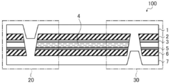
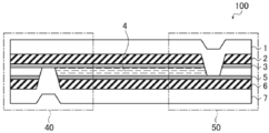
- 2 is a cross-sectional view taken along line AA in FIG. 3 is a cross-sectional view taken along line BB in FIG.
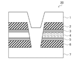
- FIG. 4 is a schematic cross-sectional view showing an embodiment of the sealing portion (first sealing portion) of the plastic cell of the present invention, including the first sealing portion surrounded by the broken line in FIG. FIG. 4 is an enlarged view of a region 20.
- FIG. 5 is a schematic cross-sectional view showing an embodiment of the sealing portion (first sealing portion) of the plastic cell of the present invention, including the first sealing portion surrounded by the broken line in FIG. 3 is an enlarged view of a region 30.
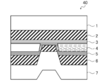
- FIG. 6 is a schematic cross-sectional view showing an embodiment of the sealing portion (second sealing portion) of the plastic cell of the present invention, including the second sealing portion surrounded by the broken line in FIG. 4 is an enlarged view of a region 40.
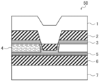
- FIG. FIG. 7 is a schematic cross-sectional view showing an embodiment of the sealing portion (second sealing portion) of the plastic cell of the present invention, including the second sealing portion surrounded by the broken line in FIG. 3. 4 is an enlarged view of a region 50.
- FIG. FIG. 8 is a schematic cross-sectional view showing an embodiment when the plastic cell of the present invention is driven.
- a numerical range expressed using “to” means a range including numerical values described before and after “to” as a lower limit value and an upper limit value.
- cutting includes “punching” and “cutting”.
- the plastic cell of the present invention includes a first plastic substrate, a first transparent conductive layer, a fluid layer, a second transparent conductive layer, and a second plastic substrate in this order.
- a part of the first plastic substrate or the second plastic substrate is deformed to seal the fluid layer, and a part of the first plastic substrate or the second plastic substrate is used.
- the sealing part containing is included.
- the sealing portion includes a first sealing portion that disconnects the first transparent conductive layer and the second transparent conductive layer, and the first transparent conductive layer and the second transparent conductive layer. And a second sealing portion for energizing any one of the layers.
- the first plastic substrate and the second plastic substrate of the plastic cell of the present invention (hereinafter simply referred to as “plastic substrate” unless otherwise required) have high moldability. It is a board
- thermoplastic resin As the thermoplastic resin, a polymer resin excellent in optical transparency, mechanical strength, thermal stability and the like is preferable.
- thermoplastic resin examples include polycarbonate polymers; polyester polymers such as polyethylene terephthalate (PET); acrylic polymers such as polymethyl methacrylate (PMMA); polystyrene, acrylonitrile / styrene copolymers (AS Styrenic polymers such as resin); and the like.
- Polyolefins such as polyethylene and polypropylene; polyolefin polymers such as norbornene resins and ethylene / propylene copolymers; amide polymers such as vinyl chloride polymers, nylons and aromatic polyamides; imide polymers; sulfone polymers; Ether sulfone polymer; polyether ether ketone polymer; polyphenylene sulfide polymer; vinylidene chloride polymer; vinyl alcohol polymer; vinyl butyral polymer; arylate polymer; polyoxymethylene polymer; epoxy polymer; And a typical cellulose-based polymer; or a copolymer obtained by copolymerizing monomer units of these polymers.
- the thermoplastic resin include a polymer obtained by mixing two or more of the polymers exemplified above.
- Both the first transparent conductive layer and the second transparent conductive layer (hereinafter simply referred to as “transparent conductive layer” unless otherwise required) included in the plastic cell of the present invention are disposed on the plastic substrate. And a conductive layer.
- “having conductivity” means that the sheet resistance value is 0.1 ⁇ / ⁇ to 10,000 ⁇ / ⁇ , and also includes what is generally called an electric resistance layer.
- the sheet resistance value is preferably low, specifically preferably 300 ⁇ / ⁇ or less, particularly preferably 200 ⁇ / ⁇ or less, and 100 ⁇ / ⁇ or less. Most preferably.
- transparent means that the transmittance is 60% or more and 99% or less.
- the transmittance of the transparent conductive layer is preferably 75% or more, particularly preferably 80% or more, and most preferably 90% or more.
- Examples of materials that can be used for the transparent conductive layer used in the present invention include metal oxides (Indium Tin Oxide: ITO, etc.), carbon nanotubes (Carbon Nanotube: CNT, Carbon Nanobud: CNB, etc.), graphene, and polymer conductors (polyacetylene). , Polypyrrole, polyphenol, polyaniline, PEDOT / PSS, etc.), metal nanowire (silver nanowire, copper nanowire, etc.), metal mesh (silver mesh, copper mesh, etc.) and the like.
- metal oxides Indium Tin Oxide: ITO, etc.
- carbon nanotubes Carbon Nanotube: CNT, Carbon Nanobud: CNB, etc.
- graphene graphene
- polymer conductors polyacetylene
- Polypyrrole polyphenol, polyaniline, PEDOT / PSS, etc.
- metal nanowire silver nanowire, copper nanowire, etc.
- metal mesh silver mesh, copper mesh, etc.
- PEDOT / PSS refers to a polymer complex in which PEDOT (a polymer of 3,4-ethylenedioxythiophene) and PSS (a polymer of styrene sulfonic acid) coexist.
- the conductive layer of the metal mesh is preferably formed by dispersing conductive fine particles such as silver and copper in a matrix rather than the conductive layer formed of only metal.
- Metal oxides such as ITO are ceramic materials, and when molding without using shrinkage as in the prior art, the problem is that cracks are easily formed by the stretching action and the sheet resistance value increases significantly. was there.
- the present invention can suppress the generation of cracks by utilizing the shrinkage, improves the problem of high sheet resistance, which has been a problem in the past, and can be used as a transparent conductive layer.
- a conductive layer in which particles such as metal mesh, carbon nanotube, and metal nanowires are dispersed in a matrix follows the shrinkage of the plastic substrate by setting the glass transition temperature (Tg) of the matrix below the shrinkage temperature of the plastic substrate.
- Tg glass transition temperature
- an alignment layer may be provided between a transparent conductive layer provided on the plastic substrate and a fluid layer described later.
- an alignment layer is provided on the outermost surfaces of the first plastic substrate and the second plastic substrate used in the plastic cell, and a function of aligning a fluid layer containing a liquid crystal compound can be provided.
- the alignment layer used in the present invention may be an alignment layer that horizontally aligns the liquid crystalline composition contained in the fluid layer when no voltage is applied, or an alignment layer that vertically aligns.
- the material and processing method of the alignment layer are not particularly limited.
- An alignment layer using a polymer, an alignment layer subjected to a silane coupling process, an alignment layer using a quaternary ammonium salt, and silicon oxide are deposited from an oblique direction.
- Various alignment layers such as an alignment layer and an alignment layer utilizing photoisomerization can be used.
- a surface treatment for the alignment layer a surface treatment by rubbing treatment, energy ray irradiation, light irradiation, or the like may be used.
- a layer using polyamic acid or polyimide As an alignment layer using a polymer, a layer using polyamic acid or polyimide; a layer using modified or non-modified polyvinyl alcohol; a layer using modified or non-modified polyacrylic acid; in the following general formula (I)
- (meth) acrylic acid is a notation representing acrylic acid or methacrylic acid.
- R 1 and R 2 are each independently a hydrogen atom, a halogen atom or an alkyl group having 1 to 6 carbon atoms; M is a proton, an alkali L 0 is a divalent selected from the group consisting of —O—, —CO—, —NH—, —SO 2 —, an alkylene group, an alkenylene group, an arylene group, and combinations thereof.
- R 0 is a hydrocarbon group having 10 to 100 carbon atoms or a fluorine atom-substituted hydrocarbon group having 1 to 100 carbon atoms; Cy is an aliphatic ring group, aromatic group or It is a heterocyclic group, preferably having a carbazole group; m is 10 to 99 mol%; and n is 1 to 90 mol%.
- an alignment layer containing any one of polyimide, compounds represented by the general formulas (I) to (III), and a silane coupling agent is advantageous in terms of alignment ability, durability, insulation, and cost. It is preferable from the viewpoint, and it is particularly preferable to use an alignment layer containing any of polyimide and a compound represented by the general formulas (I) to (III) and having a carbazole group.
- a photo-alignment layer that enables alignment treatment of liquid crystal by irradiation with polarized and non-polarized ultraviolet (UV) light may be used.
- UV ultraviolet
- the fluid layer of the plastic cell of the present invention is not particularly limited as long as it is a fluid continuous material other than gas and plasma fluid.
- a particularly preferable material state is preferably a liquid and a liquid crystal body, and a fluid layer is most preferably a liquid crystal layer formed using a liquid crystal composition containing a liquid crystal compound.
- liquid crystal compounds can be classified into a rod type and a disk type from the shape.
- Polymer generally refers to a polymer having a degree of polymerization of 100 or more (Polymer Physics / Phase Transition Dynamics, Masao Doi, 2 pages, Iwanami Shoten, 1992).
- any liquid crystal compound can be used, but a rod-like liquid crystal compound or a discotic liquid crystal compound (discotic liquid crystal compound) is preferably used.
- Two or more kinds of rod-like liquid crystalline compounds, two or more kinds of disc-like liquid crystalline compounds, or a mixture of a rod-like liquid crystalline compound and a disk-like liquid crystalline compound may be used.
- the liquid crystal compound is a mixture of two or more, it is preferable that at least one liquid crystal compound has two or more polymerizable groups in one molecule.
- the plastic cell of the present invention is preferably an embodiment in which the fluid layer is a liquid crystal layer, that is, a liquid crystal cell.
- the liquid crystal cell is a liquid crystal cell used in a liquid crystal display device used in a flat-screen television, a monitor, a notebook computer, a mobile phone, and the like, and a light intensity applied to interiors, building materials, vehicles, and the like.
- a liquid crystal cell used for an optical device is also included. That is, it is a general term for devices that drive a liquid crystal composition having a polarizability by adjusting a voltage of a liquid crystal composition or the like sealed between two substrates.
- IPS In-Plane-Switching: IPS
- vertical alignment type Virtual Alignment: VA
- twisted nematic type Twisted Nematic: TN
- super twisted nematic type TW
- Various methods including STN can be used.
- the plastic cell of this invention has the sealing part which seals the fluid layer mentioned above.
- the sealing portion since the sealing portion is formed by deforming a part of the first plastic substrate or the second plastic substrate, it includes a part of the first plastic substrate or the second plastic substrate.
- the sealing portion includes a first sealing portion where the first transparent conductive layer and the second transparent conductive layer are disconnected, a first transparent conductive layer, and a second transparent portion. A second sealing portion that energizes either one of the conductive layers.
- the sealing portion is preferably a sealing formed by heat-sealing between plastic substrates.
- a dye molecule used for changing the intensity of light in the light control element may be used in combination.
- a backlight member may be provided outside or attached to the outside of the liquid crystal cell.
- a polarizing plate member may be provided outside or attached to the outside of the liquid crystal cell.
- the planar shape of the plastic cell of the present invention may be rectangular. There are no restrictions on the size of the square or rectangle.
- the plastic cell of the present invention may have a planar shape other than a rectangle.
- it may be a circle, an ellipse, a triangle, a polygon more than a pentagon, a free shape combining straight lines and curves, and if the periphery of a plastic cell is sealed, the inside will be like a donut shape. It may be a hollow shape.
- the plastic cell of this invention can use a elongate film as a 1st and 2nd plastic substrate, it can also be made into the roll form wound up in the longitudinal direction after setting it as a plastic cell. . This can contribute to packing, shipping, transportation, etc. of the plastic cell of the present invention.
- the plastic cell of the present invention may be provided with an electrode connected to the transparent conductive layer in order to apply a driving voltage.
- a method of connecting to the lead terminal using a conductive material such as silver paste or a conductive tape can be used for connection to the transparent conductive layer.
- the plastic cell manufacturing method of the present invention includes a step of arranging a first transparent conductive layer on a long first plastic substrate (hereinafter referred to as “conductive layer”).
- placement step 1 A step of disposing the second transparent conductive layer on the long second plastic substrate (hereinafter also referred to as “conductive layer disposing step 2”); A step of disposing a fluid layer on the first transparent conductive layer (hereinafter also abbreviated as “fluid layer disposing step”); The first plastic substrate on which the first transparent conductive layer and the fluid layer are arranged and the second plastic substrate on which the second transparent conductive layer is arranged are bonded together by roll-to-roll, and a long laminate is formed.
- a step of manufacturing a body (hereinafter also abbreviated as “laminated body manufacturing step”), After the laminate is manufactured, the first and second plastic substrates are heat-sealed to seal the fluid layer in the longitudinal direction (hereinafter also abbreviated as “sealing step”), and A step of winding the laminate into a roll, The manufacturing method of the plastic cell containing this.
- conductive layer placement step 1 and conductive layer placement step 2 hereinafter simply abbreviated as “conductive layer placement step” unless otherwise required
- fluid layer placement step hereinafter simply abbreviated as “conductive layer placement step” unless otherwise required
- the conductive layer arranging step 1 of the production method of the present invention is a step of arranging the first transparent conductive layer on the long first plastic substrate, and the conductive layer arranging step 2 is the long second shape.
- the second transparent conductive layer is disposed on the plastic substrate.
- the method of disposing the transparent conductive layer on the plastic substrate is not particularly limited, and the material that can be used for the transparent conductive layer described in the plastic cell of the present invention is disposed by a method such as coating, vapor deposition, or printing. Can do.
- the fluid layer arrangement step of the manufacturing method of the present invention is a step of arranging a fluid layer on the first transparent conductive layer.
- the method of disposing the fluid layer on the first transparent conductive layer is not particularly limited, and various known methods such as coating, dipping, and injection utilizing capillary action can be used.
- the laminate manufacturing process of the manufacturing method of the present invention includes a first plastic substrate on which a first transparent conductive layer and a fluid layer are disposed, and a second plastic substrate on which a second transparent conductive layer is disposed. , And a roll-to-roll process to produce a long laminate.
- the method of bonding by roll-to-roll is not particularly limited.
- the first plastic substrate on which the first transparent conductive layer and the fluid layer are arranged, and the second on which the second transparent conductive layer is arranged For example, a method in which the plastic substrate is bonded to each other through a nip roll can be used.
- the sealing step of the manufacturing method of the present invention is a step of sealing the fluid layer in the longitudinal direction by thermally fusing the first and second plastic substrates.
- the method of heat fusion is not particularly limited as long as a method of giving energy necessary for heat fusion to the plastic substrate is used. Specific examples include a method in which a high-temperature metal element is brought into contact with a plastic substrate, a method in which a COx laser is condensed and applied to the plastic substrate, and a method in which ultrasonic waves are applied to the plastic substrate.
- Example 1 ⁇ Preparation of transparent conductive layer> A transparent conductive layer is produced on the surface of polycarbonate (PC-2151, thickness 250 ⁇ m) manufactured by Teijin Ltd. using Ag nanowires by the method described in Example 1 of US2013 / 0341074, and is made of polycarbonate. A laminate in which a plastic substrate and a transparent conductive layer made of Ag nanowires were laminated was produced.
- spacer layer dispersion was prepared according to the following formulation. ⁇ Formulation of spacer layer dispersion ⁇ Bead spacer SP-208 (manufactured by Sekisui Chemical Co., Ltd.) 100 parts by mass methyl isobutyl ketone solid content: 0.2% amount ⁇ ⁇
- the produced spacer layer dispersion was applied on each of two sets of laminates on which liquid crystal alignment layers were laminated using an applicator with a clearance of 100 ⁇ m. Then, it heated so that film surface temperature might be 60 degreeC, it dried for 1 minute, and produced 2 sets of laminated bodies which have a spacer layer.
- a liquid crystal layer composition was prepared according to the following formulation.
- ⁇ Liquid crystal layer composition ⁇ ZLI2806 (manufactured by Merck) 100 parts by mass cholesteric nonanate (manufactured by Tokyo Chemical Industry) 1.74 parts by mass G-472 (manufactured by Hayashibara) 3.00 parts by mass -------- ⁇
- the prepared liquid crystal layer composition is dropped into the center of one of the two laminates having the spacer layer prepared above, sandwiched between the laminates having the other spacer layer, and the liquid crystal layer composition by a roller.
- the top and bottom edges are applied using a handy sealer DRETEC HS-106WT (manufactured by Doritech) so that the heat source of the sealer is on the substrate side of the surface (upper surface). Sealing is performed at 300 ° C. for 5 seconds, and the left side is sealed at 300 ° C. for 2 seconds, and the right side is applied so that the heat source of the sealer is on the substrate side of the back surface (lower surface).
- a plastic cell 001 encapsulating liquid crystal was produced.
- a perspective view of the produced plastic cell 001 is shown in the plastic cell 100 of FIG. 1, a cross-sectional view taken along line AA in FIG. 1 is shown in FIG. 2, and a cross-sectional view taken along line BB in FIG.
- the sealing portion of the plastic cell 001 produced as described above was cut by a cross-section using a microtome and confirmed with a field emission scanning electron microscope (S-5200, manufactured by Hitachi High-Technologies Corporation), the upper side and the lower side were As shown in FIGS. 2, 4 and 5, the plastic substrate 1 on the front surface (upper surface) and the plastic substrate 7 on the back surface (lower surface) are directly bonded to seal the fluid layer 4, and The transparent conductive layer was disconnected by the sealing portion, and the sealing portion was formed so as to push the alignment layer, fluid layer (liquid crystal layer) and transparent conductive layer separately. On the left side, as shown in FIGS.
- the sealing portion is bonded with the alignment layers 3 and 5, and the transparent conductive layer 6 on the back surface (lower surface) side is disconnected, but the front surface (upper surface) side.
- the transparent conductive layer 2 was formed so as to be energized without being disconnected.
- the sealing portion is bonded with the alignment layers 3 and 5, and the transparent conductive layer 2 on the front surface (upper surface) side is disconnected, but the rear surface (lower surface) side.
- the transparent conductive layer 6 was formed so as to be energized without being disconnected.
- the plastic cell 001 produced as described above was confirmed to have no problem in the sealed portion even when it was bent at 90 ° near the center for confirmation of flexibility.
- the produced plastic cell 001 is connected to the electrode by applying a conductive paste 9 to the transparent conductive layer 6 of the plastic substrate 7 on the left side, and the transparent plastic substrate 1 on the right side is transparent.
- the conductive paste 10 was applied to the conductive layer 2 and a voltage of 3 V was applied, the liquid crystal was driven in response to application or non-application, and it was confirmed that the liquid crystal could be reversibly colored and decolored.
- members 8 and 11 indicate conductive wires connected to the electrodes.
- Example 1 a plastic cell 002 is manufactured in the same manner as in Example 1 except that four sides are sealed with a UV sealant (TB1220, manufactured by Three Bond) instead of heat sealing the ends. did.
- a UV sealant TB1220, manufactured by Three Bond
- Example 2 In Example 1, instead of the handy sealer DRETEC HS-106WT (manufactured by Doritech) used for heat-sealing the end seal, a table type degassing sealer (V-300, manufactured by Fuji Impulse Sales Co., Ltd.) A plastic cell 003 enclosing a liquid crystal was produced in the same manner as in Example 1 except that all four sides were sealed by thermal fusion at 200 ° C. for 1 second.
- DRETEC HS-106WT manufactured by Doritech
- the sealing portion of the plastic cell 003 produced as described above is cut with a microtome and confirmed with a field emission scanning electron microscope (S-5200, manufactured by Hitachi High-Technologies Corporation), the sealing portion is only an alignment layer. It was glued with.
Landscapes
- Physics & Mathematics (AREA)
- Nonlinear Science (AREA)
- Mathematical Physics (AREA)
- Chemical & Material Sciences (AREA)
- Crystallography & Structural Chemistry (AREA)
- General Physics & Mathematics (AREA)
- Optics & Photonics (AREA)
- Liquid Crystal (AREA)
- Spectroscopy & Molecular Physics (AREA)
- Engineering & Computer Science (AREA)
- Mechanical Engineering (AREA)
- Laminated Bodies (AREA)
Abstract
本発明は、プラスチック基板が凹凸や曲面をもつ自由な形状に変形した場合であっても、シール性を失わずに導電性を保つプラスチックセルおよびその製造方法を提供することを課題とする。本発明のプラスチックセルは、第1のプラスチック基板と、第1の透明導電層と、流体層と、第2の透明導電層と、第2のプラスチック基板と、をこの順に有し、さらに、第1のプラスチック基板または第2のプラスチック基板の一部が変形して流体層を封止し、かつ、第1のプラスチック基板または第2のプラスチック基板の一部を含む封止部分を有し、封止部分が、第1の透明導電層および第2の透明導電層を断線する第1の封止部分と、第1の透明導電層および第2の透明導電層のいずれか一方を通電する第2の封止部分とを有する、プラスチックセルである。
Description
本発明は、プラスチック基板を用いたプラスチックセルとその製造方法に関する。
近年、液晶表示装置は様々な形態へ進化しており、軽量で、曲げることができるフレキシブルディスプレイが注目されている。このようなフレキシブルディスプレイに用いられる液晶セルにおいては、従来用いられてきたガラス基板では、軽量で曲げられる要求に応えるのは困難であるため、ガラス基板の代替として各種プラスチック基板が検討されている。
また、液晶セルの用途は、包装、装飾、インテリア、建材、車両などの用途で用いられる調光装置にも広がっており、これら調光装置においても、軽くて曲げられるフレキシブル性、さらには2次元平面ではなく、凹凸や曲面をもつ自由な形状として用いることも望まれており、これらの用途における基板においても、ガラス基板の代替としてプラスチック基板の実用化が求められている。
一方、フレキシブル性を持つ液晶セルを作製しようとした場合には、その液晶セル中の液晶性化合物をシールするシール剤もフレキシブル性を持つ必要がある。
このようなフレキシブル性を持ったシール剤としては、例えば、特許文献1には、可撓性を付与したエポキシ樹脂硬化物を用いたシール剤が開示されている。
また、特許文献2には、フレキシブル支持体同士を直接熱融着させるシール方法によって、折り曲げに耐えるシール方法が開示されている。
このようなフレキシブル性を持ったシール剤としては、例えば、特許文献1には、可撓性を付与したエポキシ樹脂硬化物を用いたシール剤が開示されている。
また、特許文献2には、フレキシブル支持体同士を直接熱融着させるシール方法によって、折り曲げに耐えるシール方法が開示されている。
本発明者は、特許文献1に記載されたシール剤および特許文献2に記載された熱融着によるシール部の補強方法を検討したところ、凹凸形状や曲面形状を有するプラスチック基板を用いた場合には、シール性が失われ、液晶の駆動、すなわち導電性を保つことが困難となる場合があることを明らかとした。
そこで、本発明は、プラスチック基板が凹凸や曲面をもつ自由な形状に変形した場合であっても、シール性を失わずに導電性を保つプラスチックセルおよびその製造方法を提供することを課題とする。
そこで、本発明は、プラスチック基板が凹凸や曲面をもつ自由な形状に変形した場合であっても、シール性を失わずに導電性を保つプラスチックセルおよびその製造方法を提供することを課題とする。
本発明者は、鋭意検討の結果、プラスチックセルに用いられるシール方法に関して、プラスチックセルの上下に配置したプラスチック基板の一部を変形(例えば、熱融着)させて流体層を封止することによって、プラスチック基板が大きく変形した場合であっても、シール性を失わず、プラスチックセルの導電性を保つことができることを見出した。
すなわち、以下の構成により上記課題を達成することができることを見出した。
すなわち、以下の構成により上記課題を達成することができることを見出した。
[1] 第1のプラスチック基板と、第1の透明導電層と、流体層と、第2の透明導電層と、第2のプラスチック基板と、をこの順に有し、
さらに、第1のプラスチック基板または第2のプラスチック基板の一部が変形して流体層を封止し、かつ、第1のプラスチック基板または第2のプラスチック基板の一部を含む封止部分を有し、
封止部分が、第1の透明導電層および第2の透明導電層を断線する第1の封止部分と、第1の透明導電層および第2の透明導電層のいずれか一方を通電する第2の封止部分とを有する、プラスチックセル。
[2] 第1の透明導電層と流体層との間、および、第2の透明導電層と流体層との間に、それぞれ配向層を有し、
流体層が、液晶性化合物を含有する液晶組成物を用いて形成された液晶層である、[1]に記載のプラスチックセル。
[3] 第1のプラスチック基板および第2のプラスチック基板がいずれも長尺状のフィルムであり、
長尺状のフィルムの長手方向に巻き取られたロール形態である、[1]または[2]に記載のプラスチックセル。
[4] さらに電極を有し、
電極と、第1の透明導電層および第2の透明導電層の少なくとも一方とが接続されている、[1]~[3]のいずれかに記載のプラスチックセル。
[5] 長尺状の第1のプラスチック基板に第1の透明導電層を配置する工程、
長尺状の第2のプラスチック基板に第2の透明導電層を配置する工程、
第1の透明導電層の上に、流体層を配置する工程、
第1の透明導電層および流体層が配置された第1のプラスチック基板と、第2の透明導電層が配置された第2のプラスチック基板とを、ロールトゥロールで貼り合わせ、長尺状の積層体を作製する工程、
積層体を作製した後、第1のプラスチック基板および第2のプラスチック基板を熱融着することにより、流体層を長手方向に封止する工程、および、
積層体をロール状に巻く工程、
を含む、プラスチックセルの製造方法。
さらに、第1のプラスチック基板または第2のプラスチック基板の一部が変形して流体層を封止し、かつ、第1のプラスチック基板または第2のプラスチック基板の一部を含む封止部分を有し、
封止部分が、第1の透明導電層および第2の透明導電層を断線する第1の封止部分と、第1の透明導電層および第2の透明導電層のいずれか一方を通電する第2の封止部分とを有する、プラスチックセル。
[2] 第1の透明導電層と流体層との間、および、第2の透明導電層と流体層との間に、それぞれ配向層を有し、
流体層が、液晶性化合物を含有する液晶組成物を用いて形成された液晶層である、[1]に記載のプラスチックセル。
[3] 第1のプラスチック基板および第2のプラスチック基板がいずれも長尺状のフィルムであり、
長尺状のフィルムの長手方向に巻き取られたロール形態である、[1]または[2]に記載のプラスチックセル。
[4] さらに電極を有し、
電極と、第1の透明導電層および第2の透明導電層の少なくとも一方とが接続されている、[1]~[3]のいずれかに記載のプラスチックセル。
[5] 長尺状の第1のプラスチック基板に第1の透明導電層を配置する工程、
長尺状の第2のプラスチック基板に第2の透明導電層を配置する工程、
第1の透明導電層の上に、流体層を配置する工程、
第1の透明導電層および流体層が配置された第1のプラスチック基板と、第2の透明導電層が配置された第2のプラスチック基板とを、ロールトゥロールで貼り合わせ、長尺状の積層体を作製する工程、
積層体を作製した後、第1のプラスチック基板および第2のプラスチック基板を熱融着することにより、流体層を長手方向に封止する工程、および、
積層体をロール状に巻く工程、
を含む、プラスチックセルの製造方法。
本発明によれば、プラスチック基板が凹凸や曲面をもつ自由な形状に変形した場合であっても、シール性を失わずに導電性を保つプラスチックセルおよびその製造方法を提供することができる。
以下、本発明について詳細に説明する。
以下に記載する構成要件の説明は、本発明の代表的な実施態様に基づいてなされることがあるが、本発明はそのような実施態様に限定されるものではない。
なお、本明細書において、「~」を用いて表される数値範囲は、「~」の前後に記載される数値を下限値および上限値として含む範囲を意味する。
また、本明細書において、「裁断」には「打ち抜き」および「切り出し」等も含むものとする。
以下に記載する構成要件の説明は、本発明の代表的な実施態様に基づいてなされることがあるが、本発明はそのような実施態様に限定されるものではない。
なお、本明細書において、「~」を用いて表される数値範囲は、「~」の前後に記載される数値を下限値および上限値として含む範囲を意味する。
また、本明細書において、「裁断」には「打ち抜き」および「切り出し」等も含むものとする。
[プラスチックセル]
本発明のプラスチックセルは、第1のプラスチック基板と、第1の透明導電層と、流体層と、第2の透明導電層と、第2のプラスチック基板と、をこの順に有する。
また、本発明のプラスチックセルは、第1のプラスチック基板または第2のプラスチック基板の一部が変形して流体層を封止し、かつ、第1のプラスチック基板または第2のプラスチック基板の一部を含む封止部分を有する。
更に、本発明のプラスチックセルは、封止部分が、第1の透明導電層および第2の透明導電層を断線する第1の封止部分と、第1の透明導電層および第2の透明導電層のいずれか一方を通電する第2の封止部分とを有する。
本発明のプラスチックセルは、第1のプラスチック基板と、第1の透明導電層と、流体層と、第2の透明導電層と、第2のプラスチック基板と、をこの順に有する。
また、本発明のプラスチックセルは、第1のプラスチック基板または第2のプラスチック基板の一部が変形して流体層を封止し、かつ、第1のプラスチック基板または第2のプラスチック基板の一部を含む封止部分を有する。
更に、本発明のプラスチックセルは、封止部分が、第1の透明導電層および第2の透明導電層を断線する第1の封止部分と、第1の透明導電層および第2の透明導電層のいずれか一方を通電する第2の封止部分とを有する。
〔プラスチック基板〕
本発明のプラスチックセルが有する第1のプラスチック基板および第2のプラスチック基板(以下、特に区別を要しない場合は単に「プラスチック基板」とも略す。)は、いずれも、自由度の高い成型性を実現する観点から用いられる基板である。
プラスチックセルを作製する際に、局所的に延伸、収縮等の寸法変化が起こるため、プラスチック基板としては、熱可塑性樹脂を用いることが好ましい。
熱可塑性樹脂としては、光学的な透明性、機械的強度、熱安定性などに優れるポリマー樹脂が好ましい。
本発明のプラスチックセルが有する第1のプラスチック基板および第2のプラスチック基板(以下、特に区別を要しない場合は単に「プラスチック基板」とも略す。)は、いずれも、自由度の高い成型性を実現する観点から用いられる基板である。
プラスチックセルを作製する際に、局所的に延伸、収縮等の寸法変化が起こるため、プラスチック基板としては、熱可塑性樹脂を用いることが好ましい。
熱可塑性樹脂としては、光学的な透明性、機械的強度、熱安定性などに優れるポリマー樹脂が好ましい。
上記熱可塑性樹脂に含まれるポリマーとしては、例えば、ポリカーボネート系ポリマー;ポリエチレンテレフタレート(PET)等のポリエステル系ポリマー;ポリメチルメタクリレート(PMMA)等のアクリル系ポリマー;ポリスチレン、アクリロニトリル・スチレン共重合体(AS樹脂)等のスチレン系ポリマー;などが挙げられる。
また、ポリエチレン、ポリプロピレン等のポリオレフィン;ノルボルネン系樹脂、エチレン・プロピレン共重合体等のポリオレフィン系ポリマー;塩化ビニル系ポリマー、ナイロンや芳香族ポリアミド等のアミド系ポリマー;イミド系ポリマー;スルホン系ポリマー;ポリエーテルスルホン系ポリマー;ポリエーテルエーテルケトン系ポリマー;ポリフェニレンスルフィド系ポリマー;塩化ビニリデン系ポリマー;ビニルアルコール系ポリマー;ビニルブチラール系ポリマー;アリレート系ポリマー;ポリオキシメチレン系ポリマー;エポキシ系ポリマー;トリアセチルセルロースに代表されるセルロース系ポリマー;またはこれらのポリマーのモノマー単位で共重合させた共重合体;などが挙げられる。
また、上記熱可塑性樹脂としては、上記で例示したポリマーを2種以上混合したポリマーも例として挙げられる。
また、ポリエチレン、ポリプロピレン等のポリオレフィン;ノルボルネン系樹脂、エチレン・プロピレン共重合体等のポリオレフィン系ポリマー;塩化ビニル系ポリマー、ナイロンや芳香族ポリアミド等のアミド系ポリマー;イミド系ポリマー;スルホン系ポリマー;ポリエーテルスルホン系ポリマー;ポリエーテルエーテルケトン系ポリマー;ポリフェニレンスルフィド系ポリマー;塩化ビニリデン系ポリマー;ビニルアルコール系ポリマー;ビニルブチラール系ポリマー;アリレート系ポリマー;ポリオキシメチレン系ポリマー;エポキシ系ポリマー;トリアセチルセルロースに代表されるセルロース系ポリマー;またはこれらのポリマーのモノマー単位で共重合させた共重合体;などが挙げられる。
また、上記熱可塑性樹脂としては、上記で例示したポリマーを2種以上混合したポリマーも例として挙げられる。
〔透明導電層〕
本発明のプラスチックセルが有する第1の透明導電層および第2の透明導電層(以下、特に区別を要しない場合は単に「透明導電層」とも略す。)は、いずれも、プラスチック基板上に配置され、導電性を有する層である。
本発明において、「導電性を有する」とは、シート抵抗値が0.1Ω/□~10,000Ω/□であることをいい、一般的には電気抵抗層と呼ばれるものも含む。
また、フレキシブルディスプレイ装置等の電極として用いる場合、シート抵抗値は低いことが好ましく、具体的には300Ω/□以下であることが好ましく、200Ω/□以下であることが特に好ましく、100Ω/□以下であることが最も好ましい。
本発明のプラスチックセルが有する第1の透明導電層および第2の透明導電層(以下、特に区別を要しない場合は単に「透明導電層」とも略す。)は、いずれも、プラスチック基板上に配置され、導電性を有する層である。
本発明において、「導電性を有する」とは、シート抵抗値が0.1Ω/□~10,000Ω/□であることをいい、一般的には電気抵抗層と呼ばれるものも含む。
また、フレキシブルディスプレイ装置等の電極として用いる場合、シート抵抗値は低いことが好ましく、具体的には300Ω/□以下であることが好ましく、200Ω/□以下であることが特に好ましく、100Ω/□以下であることが最も好ましい。
本発明に用いられる透明導電層において、「透明」とは、透過率が60%以上99%以下であることを意味する。
透明導電層の透過率としては、75%以上であることが好ましく、80%以上であることが特に好ましく、90%以上であることが最も好ましい。
透明導電層の透過率としては、75%以上であることが好ましく、80%以上であることが特に好ましく、90%以上であることが最も好ましい。
本発明に用いられる透明導電層に使用できる素材としては、金属酸化物(Indium Tin Oxide:ITOなど)、カーボンナノチューブ(Carbon Nanotube:CNT、Carbon Nanobud:CNBなど)、グラフェン、高分子導電体(ポリアセチレン、ポリピロール、ポリフェノール、ポリアニリン、PEDOT/PSSなど)、金属ナノワイヤー(銀ナノワイヤー、銅ナノワイヤーなど)、メタルメッシュ(銀メッシュ、銅メッシュなど)などを挙げることができる。
ここで、「PEDOT/PSS」とは、PEDOT(3,4-エチレンジオキシチオフェンのポリマー)とPSS(スチレンスルホン酸のポリマー)を共存させたポリマーコンプレックスをいう。
また、メタルメッシュの導電層は、金属のみで形成されたものよりも、銀、銅などの導電性微粒子がマトリクスに分散されて形成されたものが好ましい。
ここで、「PEDOT/PSS」とは、PEDOT(3,4-エチレンジオキシチオフェンのポリマー)とPSS(スチレンスルホン酸のポリマー)を共存させたポリマーコンプレックスをいう。
また、メタルメッシュの導電層は、金属のみで形成されたものよりも、銀、銅などの導電性微粒子がマトリクスに分散されて形成されたものが好ましい。
ITOなどの金属酸化物は、セラミック材料であり、従来技術のように、収縮を利用せずに成型する場合には、延伸作用によって、簡単にクラックが形成されてシート抵抗値が著しく上昇する問題があった。一方、本発明は収縮を利用することでクラックの発生を抑制でき、従来問題になっていた高いシート抵抗値を示す問題を改良し、透明導電層として用いることが可能になる。
メタルメッシュ形態、カーボンナノチューブ形態、金属ナノワイヤー等の粒子をマトリクスに分散した導電層は、マトリクスのガラス転移温度(Tg)をプラスチック基板の収縮温度以下とすることで、プラスチック基板の収縮に追随しやすくすることが可能であり、金属酸化物や高分子導電体を用いた導電層よりも、シワの発生を抑制することができ、ヘイズの上昇を抑えることができるため好ましい。
〔配向層〕
本発明のプラスチックセルにおいて、プラスチック基板の上に設けた透明導電層と、後述する流体層との間に、配向層を備えていてもよい。好ましい形態として、プラスチックセルに用いる第1のプラスチック基板および第2のプラスチック基板の最表面に配向層を有し、液晶性化合物を含む流体層を配向させる機能を持たせることができる。
本発明のプラスチックセルにおいて、プラスチック基板の上に設けた透明導電層と、後述する流体層との間に、配向層を備えていてもよい。好ましい形態として、プラスチックセルに用いる第1のプラスチック基板および第2のプラスチック基板の最表面に配向層を有し、液晶性化合物を含む流体層を配向させる機能を持たせることができる。
本発明に用いられる配向層は、電圧無印加時に、流体層に含まれる液晶性組成物を水平配向させる配向層でも、垂直配向させる配向層でもよい。
配向層の素材や処理方法は特に限定されることはなく、ポリマーを用いた配向層、シランカップリング処理を施した配向層、4級アンモニウム塩を用いた配向層、酸化ケイ素を斜め方向から蒸着した配向層、光異性化を利用する配向層等、各種配向層を用いることができる。また、配向層への表面処理として、ラビング処理やエネルギー線照射や光照射などによる表面処理を用いてもよい。
配向層の素材や処理方法は特に限定されることはなく、ポリマーを用いた配向層、シランカップリング処理を施した配向層、4級アンモニウム塩を用いた配向層、酸化ケイ素を斜め方向から蒸着した配向層、光異性化を利用する配向層等、各種配向層を用いることができる。また、配向層への表面処理として、ラビング処理やエネルギー線照射や光照射などによる表面処理を用いてもよい。
ポリマーを用いた配向層としては、ポリアミック酸またはポリイミドを用いた層;変性または無変性のポリビニルアルコールを用いた層;変性または無変性のポリアクリル酸を用いた層;下記一般式(I)で表される繰り返し単位と、下記一般式(II)で表される繰り返し単位と、下記一般式(III)で表される繰り返し単位のいずれかを含む(メタ)アクリル酸コポリマーを用いた層;のいずれかであることが好ましい。
なお、「(メタ)アクリル酸」とは、アクリル酸またはメタクリル酸を表す表記である。

なお、「(メタ)アクリル酸」とは、アクリル酸またはメタクリル酸を表す表記である。
ここで、一般式(I)~(III)中、R1およびR2は、それぞれ独立に、水素原子、ハロゲン原子または炭素原子数が1乃至6のアルキル基であり;Mは、プロトン、アルカリ金属イオンまたはアンモニウムイオンであり;L0は、-O-、-CO-、-NH-、-SO2-、アルキレン基、アルケニレン基、アリーレン基およびそれらの組み合わせからなる群より選ばれる二価の連結基であり;R0は、炭素原子数が10乃至100の炭化水素基または炭素原子数が1乃至100のフッ素原子置換炭化水素基であり;Cyは、脂肪族環基、芳香族基または複素環基であり、特にカルバゾール基を有することが好ましく;mは、10乃至99モル%であり;そして、nは、1乃至90モル%である。
これらのうち、ポリイミド、一般式(I)~(III)で表される化合物、および、シランカップリング剤のいずれかを含む配向層を用いることが、配向能力、耐久性、絶縁性、コストの観点から好ましく、特にポリイミド、および、一般式(I)~(III)で表され、かつ、カルバゾール基を有する化合物のいずれかを含む配向層を用いることが好ましい。
また配向層としては、偏光および非偏光の紫外線(UV)光の照射によって液晶の配向処理が可能となる光配向層を用いてもよい。
〔流体層〕
本発明のプラスチックセルが有する流体層は、気体、プラズマ流体以外の流動性のある連続体であれば特に限定はない。
特に好ましい物質状態としては、液体、および、液晶体であることが好ましく、流体層としては、液晶性化合物を含有する液晶組成物を用いて形成された液晶層であることが最も好ましい。
ここで、一般的に、液晶性化合物はその形状から、棒状タイプと円盤状タイプに分類できる。さらにそれぞれ低分子と高分子タイプがある。高分子とは一般に重合度が100以上のものを指す(高分子物理・相転移ダイナミクス,土井 正男 著,2頁,岩波書店,1992)。本発明では、いずれの液晶性化合物を用いることもできるが、棒状液晶性化合物またはディスコティック液晶性化合物(円盤状液晶性化合物)を用いるのが好ましい。2種以上の棒状液晶性化合物、2種以上の円盤状液晶性化合物、または棒状液晶性化合物と円盤状液晶性化合物との混合物を用いてもよい。上述の液晶性化合物の固定化のために、重合性基を有する棒状液晶性化合物または円盤状液晶性化合物を用いて形成することがより好ましく、液晶性化合物が1分子中に重合性基を2以上有することがさらに好ましい。液晶性化合物が二種類以上の混合物の場合には、少なくとも1種類の液晶性化合物が1分子中に2以上の重合性基を有していることが好ましい。
本発明のプラスチックセルが有する流体層は、気体、プラズマ流体以外の流動性のある連続体であれば特に限定はない。
特に好ましい物質状態としては、液体、および、液晶体であることが好ましく、流体層としては、液晶性化合物を含有する液晶組成物を用いて形成された液晶層であることが最も好ましい。
ここで、一般的に、液晶性化合物はその形状から、棒状タイプと円盤状タイプに分類できる。さらにそれぞれ低分子と高分子タイプがある。高分子とは一般に重合度が100以上のものを指す(高分子物理・相転移ダイナミクス,土井 正男 著,2頁,岩波書店,1992)。本発明では、いずれの液晶性化合物を用いることもできるが、棒状液晶性化合物またはディスコティック液晶性化合物(円盤状液晶性化合物)を用いるのが好ましい。2種以上の棒状液晶性化合物、2種以上の円盤状液晶性化合物、または棒状液晶性化合物と円盤状液晶性化合物との混合物を用いてもよい。上述の液晶性化合物の固定化のために、重合性基を有する棒状液晶性化合物または円盤状液晶性化合物を用いて形成することがより好ましく、液晶性化合物が1分子中に重合性基を2以上有することがさらに好ましい。液晶性化合物が二種類以上の混合物の場合には、少なくとも1種類の液晶性化合物が1分子中に2以上の重合性基を有していることが好ましい。
本発明のプラスチックセルは、上述した流体層が液晶層である態様、すなわち、液晶セルであることが好ましい。
ここで、液晶セルとは、薄型テレビ、モニター、ノートパソコン、携帯電話などに用いられる液晶表示装置に用いられる液晶セル、および、インテリア、建材、車両などに適用される光の強弱を変化させる調光装置に用いられる液晶セルも含む。すなわち、2枚の基板間に封入した液晶組成物などを、電圧を調整することで、分極率をもつ液晶組成物を駆動させる装置の総称である。
ここで、液晶セルとは、薄型テレビ、モニター、ノートパソコン、携帯電話などに用いられる液晶表示装置に用いられる液晶セル、および、インテリア、建材、車両などに適用される光の強弱を変化させる調光装置に用いられる液晶セルも含む。すなわち、2枚の基板間に封入した液晶組成物などを、電圧を調整することで、分極率をもつ液晶組成物を駆動させる装置の総称である。
液晶セルの駆動モードとしては、水平配向型(In-Plane-Switching:IPS)、垂直配向型(Virtical Alignment:VA)、ツイストネマチック型(Twisted Nematic:TN)、スーパーツイストネマチック型(Super Twisted Nematic:STN)をはじめ、各種の方式を用いることができる。
〔封止部分〕
本発明のプラスチックセルは、上述した流体層を封止する封止部分を有する。
ここで、上記封止部分は、第1のプラスチック基板または第2のプラスチック基板の一部が変形して形成されるため、第1のプラスチック基板または第2のプラスチック基板の一部を含む。
また、本発明のプラスチックセルは、上記封止部分が、第1の透明導電層および第2の透明導電層を断線する第1の封止部分と、第1の透明導電層および第2の透明導電層のいずれか一方を通電する第2の封止部分とを有する。
更に、上記封止部分は、プラスチック基板同士の熱融着により形成される封止であることが好ましい。
本発明のプラスチックセルは、上述した流体層を封止する封止部分を有する。
ここで、上記封止部分は、第1のプラスチック基板または第2のプラスチック基板の一部が変形して形成されるため、第1のプラスチック基板または第2のプラスチック基板の一部を含む。
また、本発明のプラスチックセルは、上記封止部分が、第1の透明導電層および第2の透明導電層を断線する第1の封止部分と、第1の透明導電層および第2の透明導電層のいずれか一方を通電する第2の封止部分とを有する。
更に、上記封止部分は、プラスチック基板同士の熱融着により形成される封止であることが好ましい。
また、本発明のプラスチックセルのセル内部においては、調光素子において光の強弱を変化させるために用いられる色素分子などを併用してもよい。
また、液晶セルの構成に応じて、液晶セルの外部にバックライト部材や偏光板部材や表面反射を制御する部材などを併設あるいは貼合によって用いてもよい。
本発明のプラスチックセルは、平面形状を、矩形状としてもよい。正方形でも長方形でも、また大きさについても制限はない。
また、本発明のプラスチックセルは、平面形状を、矩形以外の形状としてもよい。例えば円形、楕円形、三角形、五角形以上の多角形としてもよいし、直線および曲線を組み合わせた自由な形状、またプラスチックセルの周囲が封止されているのであれば、ドーナツ型のように内部がくりぬかれた形状としてもよい。
更に、本発明のプラスチックセルは、第1および第2のプラスチック基板として長尺状のフィルムを用いることができることから、プラスチックセルとした後に、長手方向に巻き取られたロール形態とすることもできる。これは本発明のプラスチックセルの梱包、出荷、輸送などに寄与することができる。
〔電極〕
本発明のプラスチックセルは、駆動電圧を印加するため、透明導電層と接続する電極を取りつけてもよい。例えば、透明導電層との接続に銀ペーストなどの導電性素材や導電性テープなどを用いてリード端子と接続する方法などを用いることができる。
本発明のプラスチックセルは、駆動電圧を印加するため、透明導電層と接続する電極を取りつけてもよい。例えば、透明導電層との接続に銀ペーストなどの導電性素材や導電性テープなどを用いてリード端子と接続する方法などを用いることができる。
[プラスチックセルの製造方法]
本発明のプラスチックセルの製造方法(以下、「本発明の製造方法」とも略す。)は、長尺状の第1のプラスチック基板に第1の透明導電層を配置する工程(以下、「導電層配置工程1」とも略す。)、
長尺状の第2のプラスチック基板に第2の透明導電層を配置する工程(以下、「導電層配置工程2」とも略す。)、
第1の透明導電層の上に、流体層を配置する工程(以下、「流体層配置工程」とも略す。)、
第1の透明導電層および流体層が配置された第1のプラスチック基板と、第2の透明導電層が配置された第2のプラスチック基板とを、ロールトゥロールで貼り合わせ、長尺状の積層体を作製する工程(以下、「積層体作製工程」とも略す。)、
積層体を作製した後、第1および第2のプラスチック基板を熱融着することにより、流体層を長手方向に封止する工程(以下、「封止工程」とも略す。)、および、
積層体をロール状に巻く工程、
を含む、プラスチックセルの製造方法である。
以下に、導電層配置工程1および導電層配置工程2(以下、特に区別を要しない場合は単に「導電層配置工程」とも略す。)、ならびに、流体層配置工程、積層体作製工程および封止工程について詳述する。
本発明のプラスチックセルの製造方法(以下、「本発明の製造方法」とも略す。)は、長尺状の第1のプラスチック基板に第1の透明導電層を配置する工程(以下、「導電層配置工程1」とも略す。)、
長尺状の第2のプラスチック基板に第2の透明導電層を配置する工程(以下、「導電層配置工程2」とも略す。)、
第1の透明導電層の上に、流体層を配置する工程(以下、「流体層配置工程」とも略す。)、
第1の透明導電層および流体層が配置された第1のプラスチック基板と、第2の透明導電層が配置された第2のプラスチック基板とを、ロールトゥロールで貼り合わせ、長尺状の積層体を作製する工程(以下、「積層体作製工程」とも略す。)、
積層体を作製した後、第1および第2のプラスチック基板を熱融着することにより、流体層を長手方向に封止する工程(以下、「封止工程」とも略す。)、および、
積層体をロール状に巻く工程、
を含む、プラスチックセルの製造方法である。
以下に、導電層配置工程1および導電層配置工程2(以下、特に区別を要しない場合は単に「導電層配置工程」とも略す。)、ならびに、流体層配置工程、積層体作製工程および封止工程について詳述する。
〔導電層配置工程〕
本発明の製造方法が有する導電層配置工程1は、長尺状の第1のプラスチック基板に第1の透明導電層を配置する工程であり、導電層配置工程2は、長尺状の第2のプラスチック基板に第2の透明導電層を配置する工程である。
ここで、プラスチック基板に透明導電層を配置する方法は特に限定されず、本発明のプラスチックセルにおいて説明した透明導電層に使用できる素材を、例えば、塗布、蒸着、印刷などの方法により配置することができる。
本発明の製造方法が有する導電層配置工程1は、長尺状の第1のプラスチック基板に第1の透明導電層を配置する工程であり、導電層配置工程2は、長尺状の第2のプラスチック基板に第2の透明導電層を配置する工程である。
ここで、プラスチック基板に透明導電層を配置する方法は特に限定されず、本発明のプラスチックセルにおいて説明した透明導電層に使用できる素材を、例えば、塗布、蒸着、印刷などの方法により配置することができる。
〔流体層配置工程〕
本発明の製造方法が有する流体層配置工程は、第1の透明導電層の上に、流体層を配置する工程である。
ここで、第1の透明導電層の上に流体層を配置する方法は特に限定されず、例えば、塗布、ディップ、毛細管現象を利用した注入などの各種公知の方法を用いることができる。
本発明の製造方法が有する流体層配置工程は、第1の透明導電層の上に、流体層を配置する工程である。
ここで、第1の透明導電層の上に流体層を配置する方法は特に限定されず、例えば、塗布、ディップ、毛細管現象を利用した注入などの各種公知の方法を用いることができる。
〔積層体作製工程〕
本発明の製造方法が有する積層体作製工程は、第1の透明導電層および流体層が配置された第1のプラスチック基板と、第2の透明導電層が配置された第2のプラスチック基板とを、ロールトゥロール(Roll to Roll)で貼り合わせ、長尺状の積層体を作製する工程である。
ここで、ロールトゥロールで貼り合わせる方法は特に限定されず、例えば、第1の透明導電層および流体層が配置された第1のプラスチック基板と、第2の透明導電層が配置された第2のプラスチック基板とを、ニップロールの間を通して貼り合わせる方法などを用いることができる。
本発明の製造方法が有する積層体作製工程は、第1の透明導電層および流体層が配置された第1のプラスチック基板と、第2の透明導電層が配置された第2のプラスチック基板とを、ロールトゥロール(Roll to Roll)で貼り合わせ、長尺状の積層体を作製する工程である。
ここで、ロールトゥロールで貼り合わせる方法は特に限定されず、例えば、第1の透明導電層および流体層が配置された第1のプラスチック基板と、第2の透明導電層が配置された第2のプラスチック基板とを、ニップロールの間を通して貼り合わせる方法などを用いることができる。
〔封止工程〕
本発明の製造方法が有する封止工程は、第1および第2のプラスチック基板を熱融着することにより、流体層を長手方向に封止する工程である。
ここで、熱融着の方法としては、熱融着に必要なエネルギーをプラスチック基板に与える方法を用いれば特に限定されない。具体的には、高温の金属素子をプラスチック基板に接触させる方法、COxレーザーを集光させてプラスチック基板に当てる方法、超音波をプラスチック基板に当てる方法等が挙げられる。
本発明の製造方法が有する封止工程は、第1および第2のプラスチック基板を熱融着することにより、流体層を長手方向に封止する工程である。
ここで、熱融着の方法としては、熱融着に必要なエネルギーをプラスチック基板に与える方法を用いれば特に限定されない。具体的には、高温の金属素子をプラスチック基板に接触させる方法、COxレーザーを集光させてプラスチック基板に当てる方法、超音波をプラスチック基板に当てる方法等が挙げられる。
以下に実施例を挙げて本発明を具体的に説明するが、以下の実施例に示す素材、試薬、物質量とその割合、条件、操作等は、本発明の主旨から逸脱しない限りにおいて適宜変更することができる。したがって本発明の範囲は以下の実施例に制限されるものではない。
[実施例1]
<透明導電層の作製>
帝人(株)製のポリカーボネート(PC-2151、厚み250μm)の表面に、US2013/0341074号公報の実施例1に記載の方法にてAgナノワイヤーを用いて透明導電層を作製し、ポリカーボネートからなるプラスチック基板と、Agナノワイヤーからなる透明導電層とが積層された積層体を作製した。
<透明導電層の作製>
帝人(株)製のポリカーボネート(PC-2151、厚み250μm)の表面に、US2013/0341074号公報の実施例1に記載の方法にてAgナノワイヤーを用いて透明導電層を作製し、ポリカーボネートからなるプラスチック基板と、Agナノワイヤーからなる透明導電層とが積層された積層体を作製した。
<配向層の作製>
上記作製した積層体を10cm角に裁断し、液晶配向剤として、ポリアミック酸配向層塗布液(JSR製JALS684)をバーコーター#1.6を用いて塗布した。
その後、膜面温度80℃で3分間乾燥し、液晶配向層101を作製した。このとき、液晶配向層の膜厚は60nmであった。
このように作製した、プラスチック基板、透明導電層および液晶配向層がこの順で積層された積層体を2組用意した。
上記作製した積層体を10cm角に裁断し、液晶配向剤として、ポリアミック酸配向層塗布液(JSR製JALS684)をバーコーター#1.6を用いて塗布した。
その後、膜面温度80℃で3分間乾燥し、液晶配向層101を作製した。このとき、液晶配向層の膜厚は60nmであった。
このように作製した、プラスチック基板、透明導電層および液晶配向層がこの順で積層された積層体を2組用意した。
<スペーサー層の作製>
下記処方でスペーサー層分散液を作製した。
―――――――――――――――――――――――――――――――――
スペーサー層分散液の処方
―――――――――――――――――――――――――――――――――
ビーズスペーサSP-208(積水化学(株)製) 100質量部
メチルイソブチルケトン 固形分:0.2%となる量
―――――――――――――――――――――――――――――――――
下記処方でスペーサー層分散液を作製した。
―――――――――――――――――――――――――――――――――
スペーサー層分散液の処方
―――――――――――――――――――――――――――――――――
ビーズスペーサSP-208(積水化学(株)製) 100質量部
メチルイソブチルケトン 固形分:0.2%となる量
―――――――――――――――――――――――――――――――――
作製したスペーサー層分散液を、液晶配向層が積層された積層体2組のそれぞれの上にアプリケータを用いてクリアランス100μmの設定で塗布した。
その後、膜面温度が60℃になるように加熱し、1分間乾燥し、スペーサー層を有する積層体を2組作製した。
その後、膜面温度が60℃になるように加熱し、1分間乾燥し、スペーサー層を有する積層体を2組作製した。
<液晶セルの作製>
下記処方で液晶層組成物を作製した。
―――――――――――――――――――――――――――――――――
液晶層組成物
―――――――――――――――――――――――――――――――――
ZLI2806(メルク社製) 100質量部
コレステリックノナネート(東京化成工業製) 1.74質量部
G-472(林原製) 3.00質量部
―――――――――――――――――――――――――――――――――
下記処方で液晶層組成物を作製した。
―――――――――――――――――――――――――――――――――
液晶層組成物
―――――――――――――――――――――――――――――――――
ZLI2806(メルク社製) 100質量部
コレステリックノナネート(東京化成工業製) 1.74質量部
G-472(林原製) 3.00質量部
―――――――――――――――――――――――――――――――――
作製した液晶層組成物を、上記で作製したスペーサー層を有する積層体2組のうちの一方の中央に滴下し、もう一方のスペーサー層を有する積層体で挟みこみ、ローラーにて液晶層組成物を均一に広げて液晶層組成物を含む積層体とした。
その後、本積層体の4辺のうち、上辺および下辺の端部を、ハンディシーラーDRETEC HS-106WT(ドリテック社製)を用いて、シーラーの熱源が表面(上面)の基板側となるように当てて300℃5秒で熱融着により封止し、さらに左辺を300℃2秒で封止し、右辺はシーラーの熱源が裏面(下面)の基板側となるように当てて300℃2秒で封止して、液晶を封入したプラスチックセル001を作製した。作製したプラスチックセル001の斜視図を図1のプラスチックセル100に示し、図1のA-A線断面図を図2に示し、図1のB-B線断面図を図3に示す。
その後、本積層体の4辺のうち、上辺および下辺の端部を、ハンディシーラーDRETEC HS-106WT(ドリテック社製)を用いて、シーラーの熱源が表面(上面)の基板側となるように当てて300℃5秒で熱融着により封止し、さらに左辺を300℃2秒で封止し、右辺はシーラーの熱源が裏面(下面)の基板側となるように当てて300℃2秒で封止して、液晶を封入したプラスチックセル001を作製した。作製したプラスチックセル001の斜視図を図1のプラスチックセル100に示し、図1のA-A線断面図を図2に示し、図1のB-B線断面図を図3に示す。
上記のように作製したプラスチックセル001の封止部分を、ミクロトームを用いて断面切削し、電界放出形走査電子顕微鏡(S-5200、日立ハイテクノロジーズ社製)で確認したところ、上辺と下辺は、図2、図4および図5に示すように、表面(上面)のプラスチック基板1と裏面(下面)のプラスチック基板7とが直接接着して流体層4を封止しており、また、2つの透明導電層は封止部分によって断線しており、封止部分は配向層、流体層(液晶層)および透明導電層を押し分けるように形成されていた。
左辺では、図3および図6に示すように、封止部分は配向層3および5で接着されており、裏面(下面)側の透明導電層6は断線しているものの、表面(上面)側の透明導電層2は断線せず、通電するように形成されていた。
右辺では、図3および図7に示すように、封止部分は配向層3および5で接着されており、表面(上面)側の透明導電層2は断線しているものの、裏面(下面)側の透明導電層6は断線せず、通電するように形成されていた。
左辺では、図3および図6に示すように、封止部分は配向層3および5で接着されており、裏面(下面)側の透明導電層6は断線しているものの、表面(上面)側の透明導電層2は断線せず、通電するように形成されていた。
右辺では、図3および図7に示すように、封止部分は配向層3および5で接着されており、表面(上面)側の透明導電層2は断線しているものの、裏面(下面)側の透明導電層6は断線せず、通電するように形成されていた。
上記のように作製したプラスチックセル001は、フレキシブル性の確認のために中央付近で90°に折り曲げても、封止部分に問題がないことを確認した。
<駆動の確認>
作製したプラスチックセル001を、図8のプラスチックセル100に示すように、左辺側のプラスチック基板7の透明導電層6に導電ペースト9を塗布して電極に接続し、右辺側のプラスチック基板1の透明導電層2にも同様に導電ペースト10を塗布して、電圧3Vを印加したところ、印加または非印加に応じて液晶が駆動して、可逆的に着色、および、消色し駆動できることを確認した。なお、図8中、符号8および11の部材は、電極に繋がる導線を示す。
作製したプラスチックセル001を、図8のプラスチックセル100に示すように、左辺側のプラスチック基板7の透明導電層6に導電ペースト9を塗布して電極に接続し、右辺側のプラスチック基板1の透明導電層2にも同様に導電ペースト10を塗布して、電圧3Vを印加したところ、印加または非印加に応じて液晶が駆動して、可逆的に着色、および、消色し駆動できることを確認した。なお、図8中、符号8および11の部材は、電極に繋がる導線を示す。
[比較例1]
実施例1において、端部の封止を熱融着する代わりに、UVシール剤(TB1220、スリーボンド製)で4辺とも封止する以外は実施例1と同様の操作により、プラスチックセル002を作製した。
実施例1において、端部の封止を熱融着する代わりに、UVシール剤(TB1220、スリーボンド製)で4辺とも封止する以外は実施例1と同様の操作により、プラスチックセル002を作製した。
プラスチックセル002を、フレキシブル性の確認のために中央付近で90°に折り曲げたところ、シール剤が剥がれてしまい、プラスチックセル中の液晶組成物の一部が流れ出してしまった。
[比較例2]
実施例1において、端部の封止を熱融着する際に用いたハンディシーラーDRETEC HS-106WT(ドリテック社製)の代わりに、卓上型脱気シーラー(V-300、富士インパルス販売社製)を用いて、4辺いずれも200℃、1秒で熱融着により封止する以外は実施例1と同様の操作により、液晶を封入したプラスチックセル003を作製した。
実施例1において、端部の封止を熱融着する際に用いたハンディシーラーDRETEC HS-106WT(ドリテック社製)の代わりに、卓上型脱気シーラー(V-300、富士インパルス販売社製)を用いて、4辺いずれも200℃、1秒で熱融着により封止する以外は実施例1と同様の操作により、液晶を封入したプラスチックセル003を作製した。
上記のように作製したプラスチックセル003の封止部分をミクロトームを用いて断面切削し、電界放出形走査電子顕微鏡(S-5200、日立ハイテクノロジーズ社製)で確認すると、封止部分は配向層のみで接着されていた。
プラスチックセル003を、フレキシブル性の確認のために中央付近で90°に折り曲げたところ、封止部分が剥がれてしまい、プラスチックセル中の液晶組成物の一部が流れ出してしまった。
1、7 プラスチック基板
2、6 透明導電層
3、5 配向層
4 流体層
8、11 電極に繋がる導線
9、10 導電ペースト
20、30 第1の封止部分を含む領域
40、50 第2の封止部分を含む領域
100 プラスチックセル
2、6 透明導電層
3、5 配向層
4 流体層
8、11 電極に繋がる導線
9、10 導電ペースト
20、30 第1の封止部分を含む領域
40、50 第2の封止部分を含む領域
100 プラスチックセル
Claims (5)
- 第1のプラスチック基板と、第1の透明導電層と、流体層と、第2の透明導電層と、第2のプラスチック基板と、をこの順に有し、
さらに、前記第1のプラスチック基板または前記第2のプラスチック基板の一部が変形して前記流体層を封止し、かつ、前記第1のプラスチック基板または前記第2のプラスチック基板の一部を含む封止部分を有し、
前記封止部分が、前記第1の透明導電層および前記第2の透明導電層を断線する第1の封止部分と、前記第1の透明導電層および前記第2の透明導電層のいずれか一方を通電する第2の封止部分とを有する、プラスチックセル。 - 前記第1の透明導電層と前記流体層との間、および、前記第2の透明導電層と前記流体層との間に、それぞれ配向層を有し、
前記流体層が、液晶性化合物を含有する液晶組成物を用いて形成された液晶層である、請求項1に記載のプラスチックセル。 - 前記第1のプラスチック基板および前記第2のプラスチック基板がいずれも長尺状のフィルムであり、
前記長尺状のフィルムの長手方向に巻き取られたロール形態である、請求項1または2に記載のプラスチックセル。 - さらに電極を有し、
前記電極と、前記第1の透明導電層および前記第2の透明導電層の少なくとも一方とが接続されている、請求項1~3のいずれか1項に記載のプラスチックセル。 - 長尺状の第1のプラスチック基板に第1の透明導電層を配置する工程、
長尺状の第2のプラスチック基板に第2の透明導電層を配置する工程、
前記第1の透明導電層の上に、流体層を配置する工程、
前記第1の透明導電層および前記流体層が配置された前記第1のプラスチック基板と、前記第2の透明導電層が配置された前記第2のプラスチック基板とを、ロールトゥロールで貼り合わせ、長尺状の積層体を作製する工程、
前記積層体を作製した後、前記第1のプラスチック基板および前記第2のプラスチック基板を熱融着することにより、前記流体層を長手方向に封止する工程、および、
前記積層体をロール状に巻く工程、
を含む、プラスチックセルの製造方法。
Priority Applications (3)
| Application Number | Priority Date | Filing Date | Title |
|---|---|---|---|
| JP2017556105A JP6674476B2 (ja) | 2015-12-14 | 2016-12-14 | プラスチックセルおよびその製造方法 |
| CN201680073423.3A CN108474977B (zh) | 2015-12-14 | 2016-12-14 | 塑料单元及其制造方法 |
| US16/007,040 US20180292700A1 (en) | 2015-12-14 | 2018-06-13 | Plastic cell and method for manufacturing same |
Applications Claiming Priority (2)
| Application Number | Priority Date | Filing Date | Title |
|---|---|---|---|
| JP2015243542 | 2015-12-14 | ||
| JP2015-243542 | 2015-12-14 |
Related Child Applications (1)
| Application Number | Title | Priority Date | Filing Date |
|---|---|---|---|
| US16/007,040 Continuation US20180292700A1 (en) | 2015-12-14 | 2018-06-13 | Plastic cell and method for manufacturing same |
Publications (1)
| Publication Number | Publication Date |
|---|---|
| WO2017104716A1 true WO2017104716A1 (ja) | 2017-06-22 |
Family
ID=59056864
Family Applications (1)
| Application Number | Title | Priority Date | Filing Date |
|---|---|---|---|
| PCT/JP2016/087260 Ceased WO2017104716A1 (ja) | 2015-12-14 | 2016-12-14 | プラスチックセルおよびその製造方法 |
Country Status (4)
| Country | Link |
|---|---|
| US (1) | US20180292700A1 (ja) |
| JP (1) | JP6674476B2 (ja) |
| CN (1) | CN108474977B (ja) |
| WO (1) | WO2017104716A1 (ja) |
Cited By (3)
| Publication number | Priority date | Publication date | Assignee | Title |
|---|---|---|---|---|
| JP2019101375A (ja) * | 2017-12-07 | 2019-06-24 | 大日本印刷株式会社 | 調光フィルム、調光部材、車両 |
| US10690967B2 (en) * | 2016-02-22 | 2020-06-23 | Fujifilm Corporation | Plastic cell and method for manufacturing same |
| KR20240019309A (ko) * | 2021-07-01 | 2024-02-14 | 푸야오 글라스 인더스트리 그룹 컴퍼니 리미티드 | 조광 부재 및 이의 제조 방법, 광투과 어셈블리, 차량 |
Families Citing this family (1)
| Publication number | Priority date | Publication date | Assignee | Title |
|---|---|---|---|---|
| JP7210227B2 (ja) * | 2018-11-05 | 2023-01-23 | トヨタ紡織株式会社 | 車両用内外装材 |
Citations (3)
| Publication number | Priority date | Publication date | Assignee | Title |
|---|---|---|---|---|
| JPS57130011A (en) * | 1981-02-06 | 1982-08-12 | Hitachi Ltd | Production of liquid crystal element |
| JPH07325280A (ja) * | 1994-04-08 | 1995-12-12 | Dainippon Printing Co Ltd | 液晶/高分子複合型光学素子の作製方法 |
| JP2011064976A (ja) * | 2009-09-17 | 2011-03-31 | Fuji Xerox Co Ltd | 表示媒体 |
Family Cites Families (9)
| Publication number | Priority date | Publication date | Assignee | Title |
|---|---|---|---|---|
| JPS5564213A (en) * | 1978-11-07 | 1980-05-14 | Seiko Epson Corp | Liquid crystal display panel |
| JP2701629B2 (ja) * | 1991-11-01 | 1998-01-21 | カシオ計算機株式会社 | 液晶表示装置およびその製造方法 |
| JP3061543B2 (ja) * | 1994-12-29 | 2000-07-10 | 株式会社村上開明堂 | Ec素子を有した室外鏡 |
| WO2003003108A1 (en) * | 2001-06-29 | 2003-01-09 | Citizen Watch Co., Ltd. | Liquid crystal display panel and its manufacturing method |
| US7012729B2 (en) * | 2003-05-30 | 2006-03-14 | Electro Chromix, Inc. | Non planar mirrors with planar electrochromic cavity |
| JP2005227450A (ja) * | 2004-02-12 | 2005-08-25 | Seiko Epson Corp | 電気光学装置とその製造方法、及び電子機器 |
| JP2008052168A (ja) * | 2006-08-28 | 2008-03-06 | Toppan Printing Co Ltd | 液晶表示装置の製造方法 |
| JP2009103775A (ja) * | 2007-10-22 | 2009-05-14 | Hitachi Displays Ltd | 液晶表示装置 |
| KR101837714B1 (ko) * | 2011-08-10 | 2018-03-13 | 삼성디스플레이 주식회사 | 표시 장치 |
-
2016
- 2016-12-14 CN CN201680073423.3A patent/CN108474977B/zh active Active
- 2016-12-14 WO PCT/JP2016/087260 patent/WO2017104716A1/ja not_active Ceased
- 2016-12-14 JP JP2017556105A patent/JP6674476B2/ja active Active
-
2018
- 2018-06-13 US US16/007,040 patent/US20180292700A1/en not_active Abandoned
Patent Citations (3)
| Publication number | Priority date | Publication date | Assignee | Title |
|---|---|---|---|---|
| JPS57130011A (en) * | 1981-02-06 | 1982-08-12 | Hitachi Ltd | Production of liquid crystal element |
| JPH07325280A (ja) * | 1994-04-08 | 1995-12-12 | Dainippon Printing Co Ltd | 液晶/高分子複合型光学素子の作製方法 |
| JP2011064976A (ja) * | 2009-09-17 | 2011-03-31 | Fuji Xerox Co Ltd | 表示媒体 |
Cited By (4)
| Publication number | Priority date | Publication date | Assignee | Title |
|---|---|---|---|---|
| US10690967B2 (en) * | 2016-02-22 | 2020-06-23 | Fujifilm Corporation | Plastic cell and method for manufacturing same |
| JP2019101375A (ja) * | 2017-12-07 | 2019-06-24 | 大日本印刷株式会社 | 調光フィルム、調光部材、車両 |
| KR20240019309A (ko) * | 2021-07-01 | 2024-02-14 | 푸야오 글라스 인더스트리 그룹 컴퍼니 리미티드 | 조광 부재 및 이의 제조 방법, 광투과 어셈블리, 차량 |
| KR102811493B1 (ko) | 2021-07-01 | 2025-05-21 | 푸야오 글라스 인더스트리 그룹 컴퍼니 리미티드 | 조광 부재 및 이의 제조 방법, 광투과 어셈블리, 차량 |
Also Published As
| Publication number | Publication date |
|---|---|
| JP6674476B2 (ja) | 2020-04-01 |
| US20180292700A1 (en) | 2018-10-11 |
| CN108474977B (zh) | 2021-03-09 |
| CN108474977A (zh) | 2018-08-31 |
| JPWO2017104716A1 (ja) | 2018-10-04 |
Similar Documents
| Publication | Publication Date | Title |
|---|---|---|
| JP6574042B2 (ja) | プラスチックセルおよびその製造方法 | |
| JP6674476B2 (ja) | プラスチックセルおよびその製造方法 | |
| WO2017082397A1 (ja) | 液晶セル、および三次元構造液晶セル | |
| JP6674463B2 (ja) | 液晶セル、3次元構造液晶セル前駆体、および、3次元構造液晶セルの製造方法 | |
| JP6588619B2 (ja) | プラスチックセルおよびその製造方法 | |
| KR20140142453A (ko) | 탄소나노튜브 편광필름의 제조방법 및 이에 의한 탄소나노튜브 편광필름 | |
| KR101587124B1 (ko) | 액정 표시 장치 | |
| JP6606272B2 (ja) | プラスチックセルおよびその製造方法 | |
| US20190324313A1 (en) | Fluid cell, three-dimensional fluid cell, and method for manufacturing three-dimensional fluid cell | |
| CN108351548B (zh) | 液晶取向膜的制造方法及三维液晶单元的制造方法、以及三维液晶单元 | |
| JP6531177B2 (ja) | 液晶セルおよび3次元構造液晶セル | |
| CN105874380B (zh) | 光调制元件 | |
| JP6481046B2 (ja) | 三次元流体セルの製造方法 |
Legal Events
| Date | Code | Title | Description |
|---|---|---|---|
| 121 | Ep: the epo has been informed by wipo that ep was designated in this application |
Ref document number: 16875693 Country of ref document: EP Kind code of ref document: A1 |
|
| ENP | Entry into the national phase |
Ref document number: 2017556105 Country of ref document: JP Kind code of ref document: A |
|
| NENP | Non-entry into the national phase |
Ref country code: DE |
|
| 122 | Ep: pct application non-entry in european phase |
Ref document number: 16875693 Country of ref document: EP Kind code of ref document: A1 |