WO2017104507A1 - 干渉観察装置および干渉観察方法 - Google Patents
干渉観察装置および干渉観察方法 Download PDFInfo
- Publication number
- WO2017104507A1 WO2017104507A1 PCT/JP2016/086391 JP2016086391W WO2017104507A1 WO 2017104507 A1 WO2017104507 A1 WO 2017104507A1 JP 2016086391 W JP2016086391 W JP 2016086391W WO 2017104507 A1 WO2017104507 A1 WO 2017104507A1
- Authority
- WO
- WIPO (PCT)
- Prior art keywords
- beam splitter
- light
- interference
- branched light
- branched
- Prior art date
- Legal status (The legal status is an assumption and is not a legal conclusion. Google has not performed a legal analysis and makes no representation as to the accuracy of the status listed.)
- Ceased
Links
Images






Classifications
-
- G—PHYSICS
- G01—MEASURING; TESTING
- G01B—MEASURING LENGTH, THICKNESS OR SIMILAR LINEAR DIMENSIONS; MEASURING ANGLES; MEASURING AREAS; MEASURING IRREGULARITIES OF SURFACES OR CONTOURS
- G01B9/00—Measuring instruments characterised by the use of optical techniques
- G01B9/02—Interferometers
- G01B9/02041—Interferometers characterised by particular imaging or detection techniques
-
- G—PHYSICS
- G01—MEASURING; TESTING
- G01B—MEASURING LENGTH, THICKNESS OR SIMILAR LINEAR DIMENSIONS; MEASURING ANGLES; MEASURING AREAS; MEASURING IRREGULARITIES OF SURFACES OR CONTOURS
- G01B9/00—Measuring instruments characterised by the use of optical techniques
- G01B9/02—Interferometers
- G01B9/02001—Interferometers characterised by controlling or generating intrinsic radiation properties
- G01B9/02002—Interferometers characterised by controlling or generating intrinsic radiation properties using two or more frequencies
- G01B9/02004—Interferometers characterised by controlling or generating intrinsic radiation properties using two or more frequencies using frequency scans
-
- G—PHYSICS
- G01—MEASURING; TESTING
- G01N—INVESTIGATING OR ANALYSING MATERIALS BY DETERMINING THEIR CHEMICAL OR PHYSICAL PROPERTIES
- G01N15/00—Investigating characteristics of particles; Investigating permeability, pore-volume or surface-area of porous materials
- G01N15/10—Investigating individual particles
- G01N15/14—Optical investigation techniques, e.g. flow cytometry
- G01N15/1429—Signal processing
-
- G—PHYSICS
- G01—MEASURING; TESTING
- G01N—INVESTIGATING OR ANALYSING MATERIALS BY DETERMINING THEIR CHEMICAL OR PHYSICAL PROPERTIES
- G01N15/00—Investigating characteristics of particles; Investigating permeability, pore-volume or surface-area of porous materials
- G01N15/10—Investigating individual particles
- G01N15/14—Optical investigation techniques, e.g. flow cytometry
- G01N15/1429—Signal processing
- G01N15/1433—Signal processing using image recognition
-
- G—PHYSICS
- G01—MEASURING; TESTING
- G01N—INVESTIGATING OR ANALYSING MATERIALS BY DETERMINING THEIR CHEMICAL OR PHYSICAL PROPERTIES
- G01N15/00—Investigating characteristics of particles; Investigating permeability, pore-volume or surface-area of porous materials
- G01N15/10—Investigating individual particles
- G01N15/14—Optical investigation techniques, e.g. flow cytometry
- G01N15/1434—Optical arrangements
-
- G—PHYSICS
- G01—MEASURING; TESTING
- G01N—INVESTIGATING OR ANALYSING MATERIALS BY DETERMINING THEIR CHEMICAL OR PHYSICAL PROPERTIES
- G01N21/00—Investigating or analysing materials by the use of optical means, i.e. using sub-millimetre waves, infrared, visible or ultraviolet light
- G01N21/17—Systems in which incident light is modified in accordance with the properties of the material investigated
- G01N21/41—Refractivity; Phase-affecting properties, e.g. optical path length
- G01N21/45—Refractivity; Phase-affecting properties, e.g. optical path length using interferometric methods; using Schlieren methods
-
- G—PHYSICS
- G02—OPTICS
- G02B—OPTICAL ELEMENTS, SYSTEMS OR APPARATUS
- G02B21/00—Microscopes
- G02B21/06—Means for illuminating specimens
- G02B21/08—Condensers
- G02B21/14—Condensers affording illumination for phase-contrast observation
-
- G—PHYSICS
- G02—OPTICS
- G02B—OPTICAL ELEMENTS, SYSTEMS OR APPARATUS
- G02B21/00—Microscopes
- G02B21/18—Arrangements with more than one light path, e.g. for comparing two specimens
-
- G—PHYSICS
- G01—MEASURING; TESTING
- G01N—INVESTIGATING OR ANALYSING MATERIALS BY DETERMINING THEIR CHEMICAL OR PHYSICAL PROPERTIES
- G01N15/00—Investigating characteristics of particles; Investigating permeability, pore-volume or surface-area of porous materials
- G01N15/10—Investigating individual particles
- G01N2015/1006—Investigating individual particles for cytology
-
- G—PHYSICS
- G01—MEASURING; TESTING
- G01N—INVESTIGATING OR ANALYSING MATERIALS BY DETERMINING THEIR CHEMICAL OR PHYSICAL PROPERTIES
- G01N15/00—Investigating characteristics of particles; Investigating permeability, pore-volume or surface-area of porous materials
- G01N15/10—Investigating individual particles
- G01N15/14—Optical investigation techniques, e.g. flow cytometry
- G01N15/1434—Optical arrangements
- G01N2015/1454—Optical arrangements using phase shift or interference, e.g. for improving contrast
-
- G—PHYSICS
- G02—OPTICS
- G02B—OPTICAL ELEMENTS, SYSTEMS OR APPARATUS
- G02B21/00—Microscopes
- G02B21/0004—Microscopes specially adapted for specific applications
- G02B21/002—Scanning microscopes
- G02B21/0024—Confocal scanning microscopes (CSOMs) or confocal "macroscopes"; Accessories which are not restricted to use with CSOMs, e.g. sample holders
- G02B21/0052—Optical details of the image generation
- G02B21/0076—Optical details of the image generation arrangements using fluorescence or luminescence
Definitions
- One aspect of the present invention relates to an interference observation apparatus and an interference observation method.
- An interference observation apparatus that acquires an interference image of an observation object uses a Michelson interferometer or a Mach-Zehnder interferometer optical system, and light reflected or transmitted by the observation object and reference light.
- the interference image of the observation object can be acquired by causing the interference.
- the interference observation apparatus described in Non-Patent Document 1 uses an optical system of a Mach-Zehnder interferometer, branches light output from a light source into first branched light and second branched light, and first branched light. Light is transmitted through the observation object, the first branched light and the second branched light are combined, and an image of interference light generated by the combination is acquired.
- Non-Patent Document 1 When using the optical system of the Mach-Zehnder interferometer compared with the case of using the optical system of the Michelson interferometer, the optical path length difference between the first branched light and the second branched light from branching to multiplexing is adjusted. Therefore, it is difficult to realize a white light interferometer or a wavelength sweep type phase shift interferometer.
- the interference observation apparatus described in Non-Patent Document 1 does not have a function of adjusting the optical path length difference.
- An object of the present invention is to provide an interference observation apparatus and an interference observation method.
- An interference observation apparatus includes: (1) a light source whose wavelength of laser light is variable; and (2) branching the laser light output from the light source to output first branched light and second branched light.
- An interference optical system that constitutes a Mach-Zehnder interferometer, comprising: a beam splitter for branching; and a beam splitter for multiplexing that combines the first branched light and the second branched light and outputs the combined light;
- a control unit that controls the wavelength of the laser light output from the light source and adjusts the phase difference between the first branched light and the second branched light at the time of multiplexing by the multiplexing beam splitter.
- An interference observation method includes (1) a step of outputting laser light from a wavelength-variable light source (light output step), and (2) a branching beam splitter of an interference optical system that constitutes a Mach-Zehnder interferometer.
- a step of combining the split light and outputting the combined light (optical combining step); and (4) controlling the wavelength of the laser light output from the light source, and performing the first combining operation by the combining beam splitter. Adjusting the phase difference between the first branched light and the second branched light (adjustment step).
- optical adjustment can be easily performed using an optical system of a Mach-Zehnder interferometer, and an interference image of an observation target can be easily acquired.
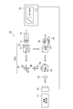
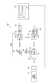
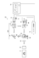
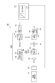
- FIG. 1 is a diagram illustrating a configuration of an interference observation apparatus 1A according to the first embodiment.
- FIG. 2 is a graph showing an example of the relationship between the laser beam wavelength and the phase difference shift amount ⁇ shift .
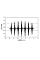
- FIG. 3 is a graph showing an example of the relationship between the combined light intensity and the optical path length difference ⁇ L when the light source 10 includes a laser diode that oscillates in the longitudinal multimode.
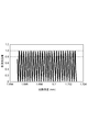
- FIG. 4 is a graph showing an enlarged horizontal axis for a part of FIG.
- FIG. 5 is a graph showing an enlarged horizontal axis for a part of FIG.
- FIG. 6 is a diagram illustrating a configuration of the interference observation apparatus 1B according to the second embodiment.
- FIG. 7 is a diagram illustrating a configuration of an interference observation apparatus 1C according to the third embodiment.
- FIG. 8 is a diagram illustrating a configuration of the interference observation apparatus 1D according to the fourth embodiment.
- FIG. 9 is a diagram illustrating a configuration of an interference observation apparatus 1E according to the fifth embodiment.
- FIG. 10 is a diagram illustrating a configuration of the interference observation apparatus 1F according to the sixth embodiment.
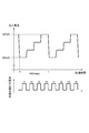
- FIG. 11 is a graph showing temporal changes in the current supplied to the laser diode of the light source 10 and the imaging period of the photodetector 61 in the example.
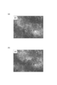
- 12A and 12B are diagrams showing interference images before intensity correction obtained in the examples (a) and (b).
- FIGS. 13A and 13B are diagrams showing interference images before intensity correction obtained in the examples (a) and (b).
- FIGS. 14A and 14B are diagrams showing interference images after intensity correction obtained in the examples (a) and (b).
- 15A and 15B are diagrams showing interference images after intensity correction obtained in the examples (a) and (b).
- FIG. 16 is a diagram illustrating a phase image before the phase unwrapping process obtained in the example.
- FIG. 17 is a diagram illustrating the phase image after the phase unwrapping process obtained in the example.
- FIG. 18 is a diagram illustrating a configuration of an interference observation apparatus 1B ′ according to a modification of the second embodiment.
- FIG. 1 is a diagram illustrating a configuration of an interference observation apparatus 1A according to the first embodiment.
- the interference observation apparatus 1A includes a light source 10, a lens 11, a lens 12, a branching beam splitter 21, a multiplexing beam splitter 22, a mirror 35, a beam splitter 41, a mirror 42, a piezo element 43, a stage 44, a lens 51, and a lens 52.
- the interference optical system 20A from the branching beam splitter 21 to the multiplexing beam splitter 22 constitutes a Mach-Zehnder interferometer.
- the photodetector 61 may be an imaging unit, for example.
- the interference observation apparatus 1A acquires an interference image based on the transmitted light of the observation object 90.
- the observation object 90 is not limited to a specific cell or biological sample.
- cultured cells immortalized cells, primary cultured cells, cancer cells, adipocytes, liver cells, cardiomyocytes, neurons, glial cells, somatic stem cells, embryonic stem cells, pluripotent stem cells, Examples include iPS cells and cell clusters (spheroids) made based on at least one of these cells.
- the observation object is not limited to a living body, but may be an industrial sample that can be measured in a transmissive configuration, for example, glass interior, semiconductor element interior, resin material, liquid crystal, polymer compound, optical element, and the like.
- the light source 10 outputs a laser beam.
- the wavelength of the laser light is variable, and the light source 10 can sweep the wavelength.
- the light source 10 may include a laser diode.
- the laser diode may be a spatial single mode laser diode or a spatial multimode laser diode.
- the lenses 11 and 12 focus the laser light output from the light source 10 on the observation object 90.
- the branching beam splitter 21 is optically coupled to the light source 10, receives the laser light output from the light source 10 and passed through the lenses 11 and 12, splits the laser light into two, and the first branched light and the second branched light. Let it be light.
- the branching beam splitter 21 may be a half mirror, for example.
- the branching beam splitter 21 outputs the first branched light to the mirror 35 of the measurement side optical system, and outputs the second branched light to the beam splitter 41 of the reference side optical system.
- the mirror 35 provided in the measurement-side optical system receives the first branched light output from the branching beam splitter 21 and reflects the first branched light to the multiplexing beam splitter 22.
- the reference side optical system is provided with a beam splitter 41, a mirror 42, a piezo element 43, and a stage 44.
- the beam splitter 41 receives the second branched light output from the branching beam splitter 21 and reflects it to the mirror 42, and receives the second branched light reflected by the mirror 42 and inputs the second branched light 22. To penetrate.
- the beam splitter 41 may be a half mirror, for example.
- the piezo element 43 can move the mirror 42 in a direction perpendicular to the reflecting surface of the mirror 42.
- the stage 44 can move the mirror 42 and the piezo element 43 in a direction perpendicular to the reflecting surface of the mirror 42.
- the piezo element 43 and the stage 44 can adjust the optical path length of the reference-side optical system, and can adjust the optical path length difference between the first branched light and the second branched light.
- the beam splitter 22 for multiplexing inputs the first branched light reflected by the mirror 35 and passed through the observation object 90 and the lens 51, and receives the second branched light outputted from the beam splitter 41 and passed through the lens 52, The first branched light and the second branched light are combined to output combined light.
- the beam splitter 22 for multiplexing may be a half mirror, for example.
- the tube lens 53 guides the combined light output from the combining beam splitter 22 to the photodetector 61 and forms an image of the combined light on the imaging surface of the photodetector 61.
- the photodetector 61 receives the combined light and outputs a detection signal, and in particular outputs a detection signal representing the intensity distribution of the combined light on the imaging surface.
- the photodetector 61 is an image sensor such as a CCD area image sensor or a CMOS area image sensor.
- the image acquisition unit 71 receives the detection signal output from the photodetector 61 and acquires an interference image of the observation object 90 based on the detection signal.
- the image acquisition unit 71 includes an image processing processor such as an FPGA (Field Programmable Gate Array) or a GPU (Graphics Processing Unit).
- the image acquisition unit 71 is, for example, a computer such as a personal computer, a smart device (for example, a tablet terminal) or a cloud server.
- the image acquisition part 71 may be provided with the display part which displays an interference image etc.
- the current control unit 72 is electrically connected to the light source 10 and controls the wavelength of the laser light output from the light source 10 by adjusting the current supplied to the light source 10. Thereby, the current control unit 72 can adjust the phase difference between the first branched light and the second branched light at the time of multiplexing by the multiplexing beam splitter 22.
- an interference image of the observation object 90 can be acquired as follows using the interference observation apparatus 1A.
- the laser light output from the light source 10 is branched into two by a branching beam splitter 21 to be a first branched light and a second branched light.
- the first branched light reflected by the mirror 35 and transmitted through the observation object 90 and the second branched light that has passed through the beam splitter 41 and the mirror 42 are multiplexed by the multiplexing beam splitter 22.
- the combined light is output from the combining beam splitter 22.
- the combined light is received by the photodetector 61, and a detection signal is output from the photodetector 61. Based on the detection signal, the image acquisition unit 71 acquires an interference image of the observation object 90.
- the wavelength of the laser light output from the light source 10 is controlled by the current control unit 72, so that the wavelength between the first branched light and the second branched light at the time of multiplexing by the multiplexing beam splitter 22. Are adjusted, and an interference image of the observation object 90 is acquired based on the detection signal.
- ⁇ L be the optical path length difference between the first branched light and the second branched light from the branching beam splitter 21 to the multiplexing beam splitter 22.
- the wavelength of the laser light is ⁇ 0
- the phase difference ⁇ 0 between the first branched light and the second branched light at the time of multiplexing by the multiplexing beam splitter 22 is expressed by the following equation (1).
- the wavelength of the laser light is ⁇ 1
- the phase difference ⁇ 1 between the first branched light and the second branched light at the time of multiplexing by the multiplexing beam splitter 22 is expressed by the following equation (2).
- mod (a, b) is a remainder (remainder) when a is divided by b.
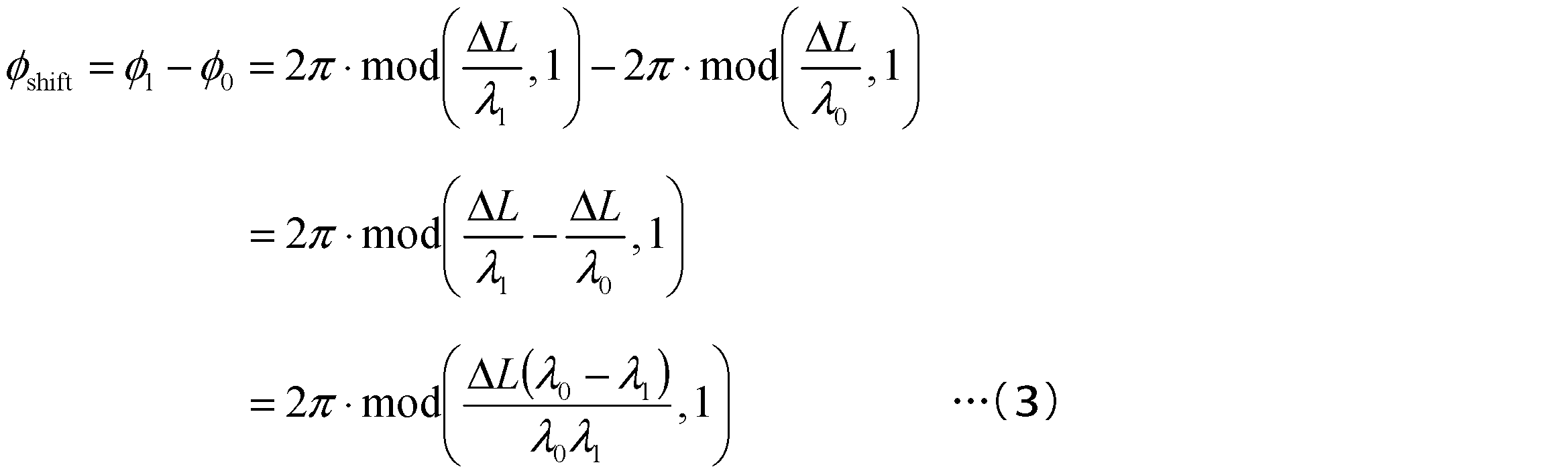
- the phase difference shift amount ⁇ shift between the first branched light and the second branched light when the wavelength of the laser light is changed from ⁇ 0 to ⁇ 1 is expressed by the following equation (3).
- the optical path length difference ⁇ L 0
- the phase difference between the first branched light and the second branched light does not change even if the wavelength of the laser light is changed.
- the phase difference shift amount ⁇ shift is equal to the optical path length difference ⁇ L. It is proportional to the product of the wavelength change amount. That is, a phase difference shift amount ⁇ shift proportional to the wavelength change amount can be realized.
- FIG. 2 is a graph showing an example of the relationship between the laser beam wavelength and the phase difference shift amount ⁇ shift .
- the phase difference between the first branched light and the second branched light at the time of multiplexing can be shifted in the range of 0 to 2 ⁇ .
- the variable range of the output light wavelength of the light source 10 is 630 nm to 630.3 nm
- the change width of the phase difference does not reach 2 ⁇ when the optical path length difference ⁇ L is 1 mm.
- the optical path length difference ⁇ L needs to be about 1.3 mm or more.
- the variable range of the output light wavelength of the light source 10 may be set to 630 nm to 630.03 nm. . It is assumed that the range in which the supply current to the light source 10 can be modulated is 50 mA to 70 mA, and the wavelength change of 630 to 630.3 nm occurs due to the adjustment of the supply current. When the wavelength is slightly changed from 630 nm to 630.03 nm, the supply current is slightly changed from 50 mA to 52 mA.
- phase shift interferometry it is necessary to divide the phase change from 0 to 2 ⁇ into four equal parts and shift the phase to 0, ⁇ / 2, ⁇ , 3 ⁇ / 2. This is because at least an accuracy of about 1/100 of the change width 2 ⁇ is required.
- an accuracy of 20 ⁇ A which is 1/100 of the supply current change width of 2 mA, is required, and it is not easy to mount such a high-accuracy current source.
- the oscillation wavelength of the laser diode depends on the temperature of the laser diode, such an excessively large optical path length difference ⁇ L becomes a condition that is vulnerable to temperature changes.
- the light source 10 when the light source 10 includes a laser diode that oscillates in a longitudinal multimode, it is more important to set the optical path length difference ⁇ L appropriately. It is known that in the interference of laser light that has oscillated in longitudinal multimode, the optical path length difference at which the degree of interference becomes maximum appears discretely. For example, in the configuration shown in FIG. 1, it is assumed that the light source 10 includes a laser diode that oscillates in a longitudinal multimode, and a photodetector 61 is disposed, and the optical path length difference ⁇ L is changed by the piezo element 43 or the stage 44.
- FIG. 3 is a graph showing an example of the relationship between the combined light intensity detected by the photodetector at this time and the optical path length difference ⁇ L.
- the optical path length difference at which the degree of interference becomes maximum appears at approximately equal intervals, but the intervals differ depending on the individual laser diodes. From this, in the phase shift Mach-Zehnder interferometer using the wavelength sweep of the light source 10, when the light source 10 includes a laser diode that oscillates in the longitudinal multimode, the optical path length difference ⁇ L is adjusted to an appropriate position in advance. Or, it is necessary for the user to make adjustments for each interference observation. Further, as described above, since the optical path length difference ⁇ L is inconvenient if it is too short or too long due to the balance with the wavelength modulation range of the light source 10, the conditions for the optical path length difference ⁇ L that can be used for measurement are limited. .
- the optical path length difference ⁇ L can be set to an appropriate value by moving the mirror 42 by the piezo element 43 or the stage 44.
- the stage 44 can coarsely adjust the optical path length difference ⁇ L
- the piezo element 43 can finely adjust the optical path length difference ⁇ L. Then, by changing the wavelength of the laser light output from the light source 10 with the optical path length difference ⁇ L set to an appropriate value, the first branched light and the first branched light at the time of multiplexing by the multiplexing beam splitter 22 are changed. The phase difference between the two-branched light can be adjusted.
- the phase difference between the first branched light and the second branched light at the time of multiplexing is adjusted by changing the wavelength of the laser light. Adjustment can be performed, and an interference image and a phase image of the observation object 90 can be easily obtained.
- the phase image can be obtained by using four interference images I 1 (x, y) to I 4 (x, y) having different phase differences by ⁇ / 2.
- the interference image I 2 (x, y) is different in phase difference by ⁇ / 2 with reference to the phase difference when acquiring the interference image I 1 (x, y), and the interference image I 3 (x, y) is ⁇
- the phase difference differs only by 3 and the interference image I 4 (x, y) differs by 3 ⁇ / 2.
- a quantitative phase image ⁇ (x, y) can be obtained from these interference images I 1 to I 4 by the following equation (4).
- X and y are variables indicating the position in each image.
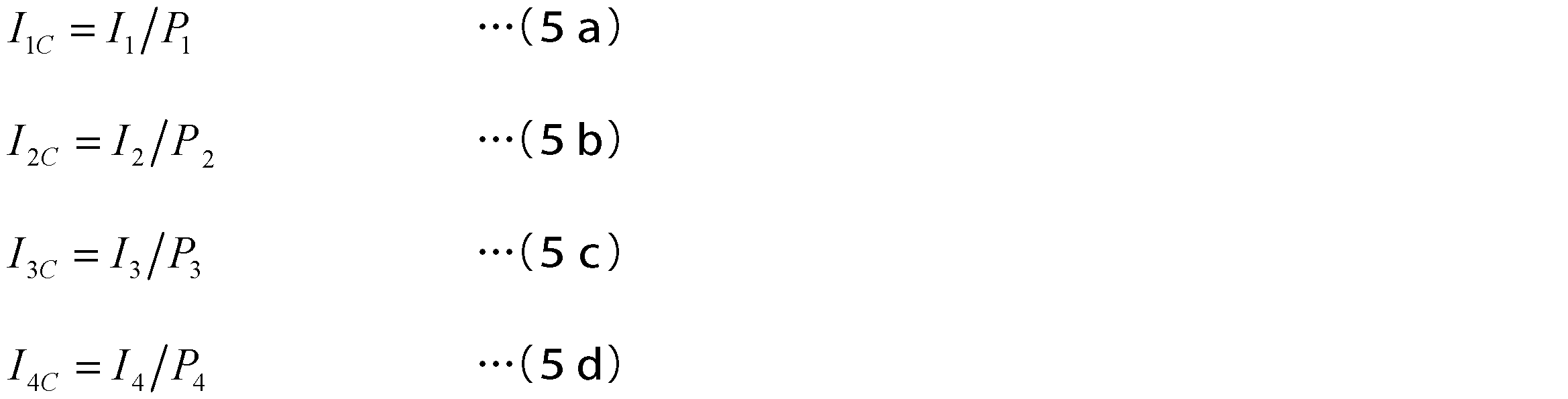
- the quantitative phase image ⁇ (x, y) obtained by the above equation (4) includes an error due to the non-constant laser light intensity between the interference images I 1 to I 4 . Therefore, by using the laser beam intensity P 1 ⁇ P 4 in acquiring respective interference image I 1 ⁇ I 4, the interference images I 1 ⁇ I 4, performs correction by the following (5a) ⁇ (5d) equation. Then, a quantitative phase image ⁇ C (x, y) is obtained from the corrected interference images I 1C to I 4C by the following equation (6). By doing in this way, the error resulting from the non-constant laser beam intensity can be removed.
- the detection result of the light emitted backward from the laser diode by the monitor photodetector built in the light source 10 is used.
- an average value of the light receiving pixel values of the photodetector 61 in a state where either one of the first branched light and the second branched light is blocked may be used.
- Each value of the laser light intensities P 1 to P 4 may be obtained by measurement at each observation, or may be obtained by measurement when the apparatus is turned on.
- each value of the laser beam intensity P 1 to P 4 is measured in advance at the time of shipment of the apparatus and stored in the storage unit of the apparatus. You may make it read and use from the memory
- FIG. 6 is a diagram showing a configuration of the interference observation apparatus 1B of the second embodiment.
- the interference observation apparatus 1B includes a light source 10, a lens 11, a lens 12, a branching beam splitter 21, a multiplexing beam splitter 22, a beam splitter 31, a mirror 32, a beam splitter 41, a mirror 42, a piezo element 43, a stage 44, and a lens. 51, a lens 52, a tube lens 53, a photodetector (light receiving unit) 61, an image acquisition unit 71, and a current control unit (control unit, controller) 72.
- the interference optical system 20B from the branching beam splitter 21 to the multiplexing beam splitter 22 constitutes a Mach-Zehnder interferometer.
- the interference optical system 20A of the interference observation apparatus 1A of the first embodiment shown in FIG. 1 includes a mirror 35, whereas the interference optical system 20B of the interference observation apparatus 1B of the second embodiment shown in FIG.
- the difference is that a beam splitter 31 and a mirror 32 are included.
- the beam splitter 31 and the mirror 32 are provided in the measurement side optical system.
- the beam splitter 31 receives the first branched light output from the branching beam splitter 21 and transmits the first branched light to the mirror 32.
- the beam splitter 31 also receives the first branched light reflected by the mirror 32 and inputs the first branched light. Reflect to.
- the beam splitter 31 may be a half mirror, for example.
- a piezo element that can move the mirror 32 in a direction perpendicular to the reflecting surface of the mirror 32 may be provided. Further, a stage that can move the mirror 32 and the piezoelectric element in a direction perpendicular to the reflecting surface of the mirror 32 may be provided.
- the first branched light is reflected by the beam splitter 31 and the mirror 32, and undergoes two image inversions.
- the second branched light is reflected by the beam splitter 41 and the mirror 42, and similarly undergoes two image inversions.
- the directions of the images of the first branched light and the second branched light at the time of multiplexing by the multiplexing beam splitter 22 coincide with each other.
- the sum of the number of image inversions due to reflection of each of the first branched light and the second branched light is an even number, each of the first branched light and the second branched light at the time of multiplexing by the multiplexing beam splitter 22 The image directions coincide with each other.
- the first branched light and the second branched light can efficiently interfere over a wide range of the imaging surface of the photodetector 61.
- the first branched light and the second branched light are in the horizontal multimode because the optical source from the light source 10 to the branching beam splitter 21 is used in addition to the case where the light source 10 oscillates in the horizontal multimode. It may change to a mode.
- the laser light output from the light source 10 is guided by a multimode optical fiber and is incident on the branching beam splitter 21, the laser light is a multimode light even when the light source 10 oscillates in a horizontal single mode. Transverse to multimode during light guiding by fiber.
- the measurement-side optical system (first branched light optical system) and the reference-side optical system (second branched light optical system) have the same configuration.
- the optical path length difference ⁇ L between the light and the second branched light can be adjusted even in the vicinity of the value 0. Therefore, the degree of freedom in setting the optical path length difference ⁇ L is high, and the degree of freedom in setting the variable range of the wavelength of the laser light output from the light source 10 is high.
- the measurement-side optical system (the first branched light optical system) and the reference-side optical system (the second branched light optical system) have the same configuration.
- the influence of the chromatic dispersion that appears can be suppressed. Accordingly, it is possible to suppress the degradation of the visibility of the interference fringes from an ideal coherence function calculated from the output light spectrum of the light source 10.
- the thickness or refractive index of the sample may change, and it may be necessary to move the stage 44 over a long distance.
- the stage 44 In order to compensate for this optical path length difference and obtain an optical path length difference that maximizes the degree of interference at the same order as before the change of the sample, the stage 44 must be moved by 802.5 ⁇ m in the direction of increasing the optical path length. Such a movement of the stage close to 1 mm causes a decrease in operability when a manual stage is used, or a heavy stepping motor stage is essential when an automatic stage is used.
- FIG. 18 is a diagram illustrating a configuration of an interference observation apparatus 1B ′ according to a modification of the second embodiment.
- the interference observation apparatus 1B ' includes an optical path length / dispersion compensation plate 91 on the reference side optical system in addition to the configuration of the interference observation apparatus 1B.
- the optical path length / dispersion compensator 91 is a plate that transmits light in accordance with variations of the sample used by the user and is made of substantially the same material as that of the sample to be used so as to have substantially the same optical path length. It is.
- a user has a cover glass having a thickness of 170 ⁇ m, a slide glass having a thickness of 1 mm, and a container having a depth of 3 mm on a plastic dish having a bottom surface thickness of 1 mm.
- an optical path length / dispersion compensation plate A for cover glass
- an optical path length / dispersion compensation plate is used as a plate that transmits light having the same optical path length as each holder.
- B for slide glass
- optical path length / dispersion compensation plate C for containers filled with water on a plastic dish
- Such optical path length / dispersion compensation plates A to C are prepared in advance.
- a cover glass having a thickness of 170 ⁇ m is a holding body
- a slide glass having a thickness of 1 mm holds the optical path length / dispersion compensation plate A.
- a cover glass having a nominal thickness of 170 ⁇ m may have a manufacturing error of ⁇ 10 ⁇ m.
- the optical path length / dispersion compensation plate 91 since the object to be measured such as cells is actually cultured on the bottom of the dish, the thickness of the cell and the culture solution The value of the optical path length varies depending on the composition. Therefore, even when the optical path length / dispersion compensation plate 91 is used, the stage 44 or a similar mechanical optical path length difference adjusting mechanism is not unnecessary.
- a stage using a differential micrometer can be preferably used.
- the differential micrometer is a micrometer in which two adjustment mechanisms of coarse movement (movable over a long distance but low resolution) and fine movement (movable only over a short distance but high resolution) are integrated.
- the coarse motion stage is fixed with an optical path length difference that maximizes the degree of interference due to the coarse motion stage without a sample.
- the optical path length / dispersion compensation plate 91 corresponding to the optical path length of the sample to be observed is inserted to obtain an optical path length difference at which the degree of interference is substantially maximized, and then only the fine movement stage is used.
- the optical path length difference so that the interference degree is strictly maximum, it is possible to obtain the interference of the laser light with an appropriate interference degree.
- the adjustment range is narrow compared to the case where the coarse movement stage is used, and there is less possibility of overlooking a point where the degree of interference becomes maximum.
- a stage using a piezo element can be preferably used.
- a piezo element has an extension distance of about 100 ⁇ m if it is long.
- the optical path length / dispersion compensation plate 91 corresponding to the optical path length of the sample to be observed is inserted to obtain an optical path length difference at which the interference level is substantially maximized, and then the stage 44 using a piezo element.
- the optical path length / dispersion compensation plate 91 can exert its effect by being inserted at an arbitrary position in the reference optical path.
- the optical path length / dispersion compensation is provided near the light source side focal point of the lens 52 of the reference side optical system.
- the insertion position of the optical path length / dispersion compensation plate 91 is near the light source side focal point of the lens 52 of the reference side optical system, but is several mm (of the focal depth of the lens 52) than the strict focal point position.
- the dust on the surface of the optical path length / dispersion compensation plate 91 can be prevented from being reflected on the imaging surface of the photodetector 61.
- the optical path length / dispersion compensation plate 91 is inserted into the folded portion for adjusting the optical path length (between the beam splitter 41 and the mirror 42)
- the reference light passes through the optical path length / dispersion compensation plate 91 twice. It is desirable to use an optical path length / dispersion compensation plate 91 manufactured so as to have an optical thickness that is half the optical thickness of the sample to be observed.
- the configuration using the optical path length / dispersion compensation plate 91 can be implemented not only as a modification of the second embodiment but also as a modification of the first embodiment described above and the third to sixth embodiments described later. .
- FIG. 7 is a diagram showing a configuration of the interference observation apparatus 1C according to the third embodiment.
- the interference observation apparatus 1C includes a light source 10, a lens 11, a lens 12, a branching beam splitter 21, a multiplexing beam splitter 22, an image inverting prism 36, a beam splitter 41, a mirror 42, a piezo element 43, a stage 44, a lens 51, A lens 52, a tube lens 53, a photodetector (light receiving unit) 61, an image acquisition unit 71, and a current control unit (control unit, controller) 72 are provided.
- the interference optical system 20C from the branching beam splitter 21 to the multiplexing beam splitter 22 constitutes a Mach-Zehnder interferometer.
- the interference optical system 20A of the interference observation apparatus 1A of the first embodiment shown in FIG. 1 includes a mirror 35, whereas the interference optical system 20C of the interference observation apparatus 1C of the third embodiment shown in FIG. The difference is that the image reversing prism 36 is included.
- the image inverting prism 36 is provided in the measurement side optical system.
- the image inverting prism 36 is, for example, a pentaprism.
- the image inversion prism 36 is a polygonal prism having a first side surface 36a, a second side surface 36b, a third side surface 36c, and a fourth side surface 36d.
- the image inverting prism 36 transmits the first branched light reaching from the branching beam splitter 21 from the first side surface 36a to the inside, and sequentially reflects the first branched light on the second side surface 36b and the third side surface 36c. Thereafter, the first branched light is transmitted from the fourth side surface 36d to the outside and output to the beam splitter 22 for multiplexing.
- the first branched light is reflected twice by the image inverting prism 36, it undergoes two image inversions.
- the second branched light is reflected by the beam splitter 41 and the mirror 42, and similarly undergoes two image inversions.
- the first branch at the time of multiplexing by the multiplexing beam splitter 22 is used. Even if the directions of the images of the light and the second branched light coincide with each other and are spatially multimode (transverse multimode), the first branched light and the second branched light are on the imaging surface of the photodetector 61. Interference can be efficiently performed in a wide range.
- the optical path length difference ⁇ L between the first branched light and the second branched light can be adjusted in the vicinity of the value 0. Therefore, the degree of freedom in setting the optical path length difference ⁇ L is high, and the degree of freedom in setting the variable range of the wavelength of the laser light output from the light source 10 is high.
- FIG. 8 is a diagram showing a configuration of the interference observation apparatus 1D of the fourth embodiment.
- the interference observation apparatus 1D includes a light source 10, a lens 11, a lens 12, a branching beam splitter 21D, a multiplexing beam splitter 22, a mirror 35, an optical rotator 37, a beam splitter 41D, a mirror 42, a piezo element 43, a stage 44, and an optical rotation. It includes a child 47, a lens 51, a lens 52, a tube lens 53, a photodetector (light receiving unit) 61, an image acquisition unit 71, and a current control unit (control unit, controller) 72.
- the interference optical system 20D from the branching beam splitter 21D to the multiplexing beam splitter 22 constitutes a Mach-Zehnder interferometer.
- the interference observation apparatus 1D of the fourth embodiment shown in FIG. Compared with the configuration of the interference observation apparatus 1A of the first embodiment shown in FIG. 1, the interference observation apparatus 1D of the fourth embodiment shown in FIG. The difference is that the beam splitter 41D is provided in place of the beam splitter 41, and that the optical rotator 37 and the optical rotator 47 are further provided.
- the branching beam splitter 21D is a polarization beam splitter.
- the branching beam splitter 21D receives the laser beam output from the light source 10 and passed through the lenses 11 and 12, and splits the laser beam into a p-polarized component and an s-polarized component.
- the branching beam splitter 21D transmits the first branched light (p-polarized component) and outputs it to the mirror 35, reflects the second branched light (s-polarized component) and outputs it to the beam splitter 41D.
- the beam splitter 41D is also a polarization beam splitter.
- the beam splitter 41D receives the second branched light (s-polarized component) output from the branching beam splitter 21D and reflects it to the mirror 42.
- the optical rotator 47 is provided on the optical path of the second branched light between the beam splitter 41D and the mirror 42.
- the optical rotator 47 may be a Faraday rotator, for example.
- the optical rotator 47 and the mirror 42 may be integrated, for example, a Faraday mirror.
- the optical rotator 47 rotates the polarization plane of the second branched light transmitted from the beam splitter 41D to the mirror 42 by 45 °, and rotates the polarization plane of the second branched light transmitted from the mirror 42 to the beam splitter 41D by 45 °. . Accordingly, the second branched light input from the optical rotator 47 to the beam splitter 41D becomes a p-polarized component.
- the beam splitter 41D transmits the second branched light (p-polarized component) and outputs it to the multiplexing beam splitter 22.
- the optical rotator 37 is provided on the optical path of the second branched light between the observation object 90 and the multiplexing beam splitter 22.
- the optical rotator 37 may be a Faraday rotator, for example.
- the optical rotator 37 rotates the polarization plane of the first branched light.
- the first branched light is p-polarized light before being transmitted through the observation object 90, but may be different from p-polarized light after being transmitted through the observation object 90.
- the optical rotator 37 rotates the polarization plane of the first branched light by a necessary angle, so that the polarization directions of the first branched light and the second branched light at the time of multiplexing by the multiplexing beam splitter 22 are changed. Match each other.
- the intensity of the combined light is monitored while changing the rotation angle of the polarization plane of the first branched light by the optical rotator 37.
- the rotation angle of the polarization plane of the first branched light may be adjusted so that the intensity of the wave light is maximized.
- a polarization beam splitter is used as the branching beam splitter 21D and the beam splitter 41D, and a second optical rotator 47 is provided on the optical path of the second branched light between the beam splitter 41D and the mirror 42, so that the second Loss in the amount of branched light can be suppressed.
- FIG. 9 is a diagram illustrating a configuration of the interference observation apparatus 1E according to the fifth embodiment.
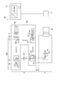
- the interference observation apparatus 1E includes a light source 10, a lens 11, a lens 12, a monitor photodetector 13, a branching beam splitter 21, a multiplexing beam splitter 22, a mirror 35, a beam splitter 41, a mirror 42, a piezo element 43, and a stage. 44, lens 51, lens 52, tube lens 53, photodetector (light receiving unit) 61, photodetector (light receiving unit) 62, image acquisition unit 71, current control unit (control unit, controller) 72, and feedback control unit ( A control unit 73).
- the interference optical system 20A from the branching beam splitter 21 to the multiplexing beam splitter 22 constitutes a Mach-Zehnder interferometer.
- the interference observation apparatus 1E of the fifth embodiment shown in FIG. 9 includes a monitoring photodetector 13, a photodetector 62, and feedback. The difference is that a control unit 73 is further provided.
- the monitor photodetector 13 detects the intensity of the laser beam output from the light source 10 and outputs the detection signal.
- the monitoring photodetector 13 only needs to detect the intensity of the light emitted backward from the laser diode.
- the combining beam splitter 22 combines the first branched light and the second branched light, outputs a part of the combined light to the photodetector 61, and outputs a part to the photodetector 62.
- the photodetector 62 receives the combined light and outputs a detection signal indicating the intensity of the combined light.
- the photodetector 62 is, for example, a photodiode or a photomultiplier tube.
- the feedback control unit 73 drives the piezo element 43 and / or the stage 44 based on the combined light intensity indicated by the detection signal output from the photodetector 62 to control the position of the mirror 42 to control the optical path.
- the phase difference is adjusted by adjusting the length difference or controlling the laser light wavelength by the current supplied from the current control unit 72 to the light source 10.
- the feedback control unit 73 corrects the combined light intensity indicated by the detection signal output from the photodetector 62 based on the laser light intensity indicated by the detection signal output from the monitoring photodetector 13. Is preferred.
- phase difference blur caused by disturbance in the optical system is detected, and phase locking and phase shifting are performed by controlling the position of the mirror 42 or controlling the laser light wavelength by the feedback control unit 73, thereby observing the object 90.
- the interference image and the phase image are acquired.
- the technique for maintaining the phase difference between the first branched light and the second branched light at the time of multiplexing is referred to as “phase lock”, and the optical path length difference maintained by the phase lock by the feedback control.
- the technique for changing the value is called “phase shift”.
- the disturbance mentioned here is not only due to mechanical vibration of the optical system, but also the optical path length due to the vibration of the boundary between the liquid surface and air when the observation object 90 is a cell in the liquid. Blur is also included.
- the control by the feedback control unit 73 will be described in detail below.
- first phase lock technology the technology described in Non-Patent Documents 2, 3, and 4 (hereinafter referred to as “first phase lock technology”) can be used.
- the phase lock technique described in these non-patent documents vibrates the mirror 42 with a sufficiently small amplitude compared with the wavelength of the output light of the light source 10 at a high speed sinusoidally, and is output from the photodetector 62 at that time.
- the phase of the interference light is obtained by synchronously detecting the detected signal with the first and second harmonics of the vibration frequency of the mirror 42.
- the feedback control unit 73 can lock the phase difference by performing feedback control so that the obtained phase value approaches the target value.
- the feedback control unit 73 inputs a detection signal which is an analog signal from the photodetector 62 and outputs an analog signal for driving and controlling the piezo element 43 or the stage 44.
- the feedback control unit 73 may perform analog processing inside or may perform digital processing. In the latter case, for example, the feedback control unit 73 converts the input detection signal into a digital signal, processes the digital signal, DA converts the digital signal obtained by the processing into an analog signal, An analog signal may be output.
- a microprocessor or FPGA Field Programmable Gate Gate Array
- the intensity V of light received by the photodetector 62 is expressed by the following equation (7).
- the received light intensity V includes an offset component DC and an amplitude AC, both of which are unknown numbers. Therefore, it is necessary to extract the phase difference ⁇ without including DC and AC by some processing.
- the intensity V of light received by the photodetector 62 is expressed by the following equation (8). Is done. ⁇ is a modulation degree determined according to the amplitude of vibration of the mirror 42. ⁇ is the angular frequency of vibration. t is a time variable.
- Equation (9a) to (9c) are obtained as approximate equations.
- J 1 and J 2 are first-type Bessel functions.
- the second term on the right side of equation (9a) vibrates with amplitude A ⁇ t and angular frequency ⁇ .
- the third term on the right side of the equation (9a) vibrates with the amplitude A 2 ⁇ t and the angular frequency 2 ⁇ . Therefore, the amplitude A ⁇ t can be obtained by synchronously detecting the detection signal output from the photodetector 62 at the angular frequency ⁇ , and the amplitude A 2 ⁇ t can be obtained by synchronously detecting the detection signal at the angular frequency 2 ⁇ . it can.
- the ratio between the amplitude A ⁇ t and the amplitude A 2 ⁇ t is expressed by the following equation (10).
- AC represents the interference intensity of the combined light, and the interference intensity AC is expressed by the following equation (11). Since the vibration amplitude of the mirror 42 is constant, J 1 ( ⁇ ) and J 2 ( ⁇ ) can be obtained based on the amplitude.
- the phase difference ⁇ corresponding to the optical path length difference can be obtained based on the equation (10), and the interference intensity AC can also be obtained based on the equation (11).
- the feedback control unit 73 includes a synchronous detection circuit, an addition circuit, and a multiplication / division circuit in order to perform the above processing.
- phase lock technique using a “spatial filtering detector” described in Non-Patent Document 5 can also be employed.
- the photodetector 62 uses a one-dimensional photodetector (light receiving unit).
- a one-dimensional photodetector include a line sensor or a multi-anode photomultiplier tube and a plurality of photodetectors arranged in a one-dimensional direction.
- Interference fringes appear by giving an inclination to either or either of the measurement side optical system and the reference side optical system.
- the received light intensities V 1 to V 4 of the four photodetectors are as follows (12a ) To (12d) to adjust the inclination of the interference fringes.
- the mirror 35 or the mirror 42 may be inclined, any lens may be inclined, Wedge-shaped prisms having different thicknesses along a predetermined direction may be inserted on the optical path.
- a 1 and A 2 are obtained by the following equations (13a) and (13b), and the ratio between A 1 and A 2 is obtained by the following equation (14). Further, the interference intensity AC is expressed by the following equation (15). From these equations, the phase difference ⁇ corresponding to the optical path length difference can be obtained, and the interference intensity AC can also be obtained.
- the feedback control unit 73 can realize the above processing with a simple electric circuit system.
- the feedback control unit 73 obtains the phase difference ⁇ according to the equations (7) to (11) based on the detection signal output from the photodetector 62 when performing the phase lock by the first phase lock technique.
- the mirror 42 may be vibrated at high speed in a sine wave manner by driving the piezo element 43 or the stage 44, and the optical path length difference may be sine wave modulated, or the current supplied from the current control unit 72 to the light source 10. May be modulated sinusoidally at high speed to modulate the laser light wavelength.
- the feedback control unit 73 performs phase locking using the first phase locking technique or the second phase locking technique, so that the obtained phase difference ⁇ is maintained constant.
- the optical path length difference may be adjusted by controlling the position of the mirror 42 by driving, or the laser light wavelength may be adjusted by controlling the current supplied from the current control unit 72 to the light source 10.
- the feedback control unit 73 modulates the current supplied from the current control unit 72 to the light source 10 at high speed sinusoidally and outputs the result from the photodetector 62 when performing phase locking by the first phase locking technique.
- the phase difference ⁇ may be obtained based on the detection signal, and the current supplied from the current control unit 72 to the light source 10 may be controlled to keep the phase difference ⁇ constant.
- the current supplied from the current control unit 72 to the light source 10 is obtained by correcting the offset current for phase shift according to the phase difference ⁇ , and adding a small amplitude and high speed sinusoidal modulation current to the current. Are superimposed.
- the light source 10 includes a laser diode
- the current supplied to the laser diode changes, not only the laser beam wavelength but also the laser beam intensity changes. Therefore, when the feedback control unit 73 modulates the current supplied from the current control unit 72 to the light source 10 at high speed sinusoidally or when the current is controlled to maintain the phase difference ⁇ constant,
- the combined light intensity indicated by the detection signal output from the light detector 62 is divided by the laser light intensity indicated by the detection signal output from the monitoring light detector 13, and the phase lock is performed based on the combined light intensity after the division. Is preferably performed.
- FIG. 10 is a diagram illustrating a configuration of the interference observation apparatus 1F according to the sixth embodiment.
- the interference observation apparatus 1F includes a light source 10, a lens 11, a lens 12, a branching beam splitter 21, a multiplexing beam splitter 22, a beam splitter 31, a mirror 32, a beam splitter 41, a mirror 42, a piezo element 43, a stage 44, and a lens. 51, a lens 52, a tube lens 53, a photodetector (light receiving unit) 61, an image acquisition unit 71, and a current control unit (control unit, controller) 72.
- the interference optical system 20F from the branching beam splitter 21 to the multiplexing beam splitter 22 in this embodiment constitutes a Mach-Zehnder interferometer, and has the same configuration as the interference optical system 20B in the second embodiment. Have.
- the light source 10 and the interference optical system 20F are held by the casing 80. Further, the housing 80 is provided with a first attachment portion 81.
- the first mounting portion 81 has an opening for outputting the combined light output from the combining beam splitter 22 of the interference optical system 20F to the outside.
- the interference optical device 2 includes the light source 10, the interference optical system 20F, the housing 80, and the first mounting portion 81.
- the microscope apparatus 3 includes the tube lens 53, the photodetector 61, the mirror 54, and the second mounting portion 82.
- the second attachment portion 82 has an opening that is optically coupled to the opening of the first attachment portion 81, and can be optically coupled to the first attachment portion 81.
- the photodetector 61 receives the combined light output from the interference optical system 20F and outputs a detection signal.
- the combined light output from the interference optical system 20F is received by the photodetector 61 through the opening of the first mounting portion 81, the opening of the second mounting portion 82, the mirror 54, and the tube lens 53.
- a commercially available microscope device 3 can be used.
- the attachment portion to which the objective lens is attached in a normal commercially available microscope apparatus may be the second attachment portion 82 described above.
- the interference observation device 1F can be configured by combining the interference optical device 2 that is downsized and integrated with the light source 10 and the interference optical system 20F held by the housing 80 and the normal microscope device 3. it can. In the present embodiment, since the existing microscope apparatus 3 can be used, the interference observation apparatus 1F can be configured at low cost.
- the beam splitter 31, the observation object 90, the multiplexing beam splitter 22, the opening of the first mounting portion 81 and the opening of the second mounting portion 82 are arranged in a vertical row. Therefore, the bright field image of the observation object 90 can be acquired by the photodetector 61 by illuminating the observation object 90 with the illumination device provided above the beam splitter 31. Further, when the microscope apparatus 3 is a fluorescence microscope, the fluorescence image of the observation object 90 is detected by illuminating and exciting the observation object 90 with an excitation illumination apparatus provided below the beam splitter 22 for multiplexing. It can be obtained by the device 61.
- the interference optical system 20A from the branching beam splitter 21 to the multiplexing beam splitter 22 is used.
- 20E and the light source 10 may be held by a housing to form an interference optical device, and the interference optical device and the microscope device 3 may be optically coupled to each other.
- the observation object 90 is a glass plate with lines drawn with oil-based ink.
- the light source 10 a multimode laser diode having an oscillation wavelength of 638 nm was used.
- FIG. 11 is a graph showing temporal changes in the current supplied to the laser diode of the light source 10 and the imaging period of the photodetector 61 in the example.
- the temporal change in the current supplied to the light source 10 is a four-step modulation waveform.
- the minimum value of the supply current was 83 mA
- the maximum value of the supply current was 92 mA
- the step width was 3 mA.
- One period of the modulation waveform was 160 msec, the period of each step was 40 msec, and the exposure time of the photodetector 61 was 20 msec.
- the optical path length difference between the first branched light and the second branched light was about 12 mm.
- FIG. 12 and 13 are diagrams showing interference images before intensity correction.
- the interference image I 2 (x, y) shown in FIG. 12B differs from the interference image I 1 (x, y) shown in FIG. 12A by a phase of ⁇ / 2, and FIG. ) interference image I 3 as shown in (x, y) have different phase by [pi, interference images I 4 (x, y) shown in FIG. 13 (b) phase differ by 3 [pi] / 2. From these images, it can be seen that the phase of the interference fringes is modulated by the supply current modulation.
- the intensity modulation amount of the laser light was examined.
- the intensity of the laser light was 88.1, 92.5, 94.6, and 94.9 in arbitrary units in order from the low supply current.
- the interference fringe image of FIGS. 12 and 13 was divided by this intensity modulation amount to obtain an interference image after intensity correction.
- the interference image I 2 (x, y) shown in FIG. 14B differs from the interference image I 1 (x, y) shown in FIG. 14A by a phase of ⁇ / 2, and FIG.
- the phase of the interference image I 3 (x, y) shown in FIG. 15 is different by ⁇
- the phase of the interference image I 4 (x, y) shown in FIG. 15B is different by 3 ⁇ / 2.
- FIG. 16 is a diagram illustrating a phase image before the phase unwrapping process.
- FIG. 17 is a diagram illustrating a phase image after the phase unwrapping process.
- a region having a long optical path length (a region having a low density) from the lower left to the upper right is a trace of oil-based pen ink drawn on the glass plate of the observation object 90.
- the interference observation apparatus and the interference observation method according to the present invention are not limited to the above-described embodiments and configuration examples, and various modifications are possible.
- a laser beam is output and the wavelength of the laser beam is variable; and (2) the laser beam output from the light source is branched to generate a first branched beam and a first beam.
- An interference optical system that constitutes a Mach-Zehnder interferometer, including a branching beam splitter that outputs two-branched light, and a combining beam splitter that combines the first branched light and the second branched light and outputs the combined light
- a control unit that controls the wavelength of the laser light output from the light source and adjusts the phase difference between the first branched light and the second branched light at the time of multiplexing by the multiplexing beam splitter. It is set as the structure provided with these.
- a light source whose wavelength of laser light is variable, and (2) a laser light output from the light source is branched to output first branched light and second branched light.
- An interference optical system that constitutes a Mach-Zehnder interferometer, comprising: a beam splitter for branching; and a beam splitter for multiplexing that combines the first branched light and the second branched light and outputs the combined light;
- a control unit that controls the wavelength of the laser light output from the light source and adjusts the phase difference between the first branched light and the second branched light at the time of multiplexing by the multiplexing beam splitter. It is said.
- the interference observation apparatus may further include a light receiving unit that receives the combined light and outputs a detection signal.
- the interference observation apparatus may further include an image acquisition unit that acquires an interference image of an observation object placed on the optical path of the first branched light or the second branched light based on the detection signal.
- the interference observation apparatus includes (1) a housing that holds the light source and the interference optical system, and (2) a first opening that is provided in the housing and outputs the combined light output from the interference optical system to the outside.
- An attachment portion (3) a second attachment portion having an opening optically coupled to the opening of the first attachment portion; and an output of the first attachment portion and the opening of the second attachment portion output from the interference optical system. It is good also as a structure provided with the microscope apparatus containing the light-receiving part which light-receives combined light and outputs a detection signal.
- (1) laser light is output from a wavelength-variable light source
- the first branched light and the second branched light are output by branching, and the first branched light and the second branched light are combined by the combining beam splitter to output the combined light.
- (3) The combined light is received by the light receiving unit. Receives the wave light and outputs a detection signal.
- (1) laser light is output from a wavelength-variable light source, and (2) the laser is output from the light source by the branching beam splitter of the interference optical system constituting the Mach-Zehnder interferometer. Branching the light into a first branched light and a second branched light; (3) combining the first branched light and the second branched light with a beam splitter for multiplexing of the interference optical system, and outputting the combined light; (4) The wavelength of the laser light output from the light source is controlled to adjust the phase difference between the first branched light and the second branched light at the time of multiplexing by the multiplexing beam splitter.
- the light source may include a laser diode that oscillates in a longitudinal multimode.
- the interference optical system includes a first beam splitter and a first mirror on the optical path of the first branch light, and the first branch that reaches the first beam splitter from the branch beam splitter.
- the light is transmitted or reflected by the first beam splitter and then reflected by the first mirror, and the first branched light reflected by the first mirror and reaching the first beam splitter is reflected or transmitted by the first beam splitter,
- a configuration may be employed in which the first branched light is output from the first beam splitter in a direction different from the input direction of the first branched light from the branching beam splitter to the first beam splitter.
- the interference optical system includes a second beam splitter and a second mirror on the optical path of the second branch light, and the second branch reaching the second beam splitter from the branch beam splitter.
- the light is transmitted or reflected by the second beam splitter and then reflected by the second mirror, and the second branched light reflected by the second mirror and reaching the second beam splitter is reflected or transmitted by the second beam splitter,
- a configuration may be adopted in which the second branched light is output from the second beam splitter in a direction different from the input direction of the second branched light from the branching beam splitter to the second beam splitter.
- the observation target is disposed on one of the first branched light and the second branched light, and the optical path length / dispersion compensation plate is provided on the other optical path.
- the optical path length / dispersion compensation plate may be configured to compensate for the change in the optical path length due to the arrangement of the observation object and the influence of dispersion.
- the present invention can be used as an interference observation apparatus and an interference observation method that can easily perform optical adjustment using an optical system of a Mach-Zehnder interferometer and can easily acquire an interference image of an observation object.
Landscapes
- Physics & Mathematics (AREA)
- Chemical & Material Sciences (AREA)
- General Physics & Mathematics (AREA)
- Analytical Chemistry (AREA)
- Biochemistry (AREA)
- Health & Medical Sciences (AREA)
- Life Sciences & Earth Sciences (AREA)
- General Health & Medical Sciences (AREA)
- Immunology (AREA)
- Pathology (AREA)
- Dispersion Chemistry (AREA)
- Optics & Photonics (AREA)
- Engineering & Computer Science (AREA)
- Signal Processing (AREA)
- Instruments For Measurement Of Length By Optical Means (AREA)
- Investigating Or Analysing Materials By Optical Means (AREA)
- Microscoopes, Condenser (AREA)
Abstract
干渉観察装置1Aは、光源10、分岐用ビームスプリッタ21、合波用ビームスプリッタ22、ミラー35、ビームスプリッタ41、ミラー42、ピエゾ素子43、ステージ44、光検出器61、画像取得部71および電流制御部72を備える。分岐用ビームスプリッタ21から合波用ビームスプリッタ22に到る迄の干渉光学系20Aは、マッハツェンダ干渉計を構成している。電流制御部72は、光源10から出力されるレーザ光の波長を制御して、合波用ビームスプリッタ22による合波の際の2つの分岐光成分の間の位相差を調整する。これにより、マッハツェンダ干渉計の光学系を用いて容易に光学調整をすることができ容易に観察対象物の干渉画像を取得することができる干渉観察装置および干渉観察方法が実現される。
Description
本発明の一側面は、干渉観察装置および干渉観察方法に関するものである。
観察対象物の干渉画像を取得する干渉観察装置は、マイケルソン(Michelson)干渉計またはマッハツェンダ(Mach-Zehnder)干渉計の光学系を用いて、観察対象物で反射または透過した光と参照光とを干渉させることで、観察対象物の干渉画像を取得することができる。非特許文献1に記載された干渉観察装置は、マッハツェンダ干渉計の光学系を用いるものであって、光源から出力された光を分岐して第1分岐光および第2分岐光とし、第1分岐光を観察対象物で透過させ、第1分岐光と第2分岐光とを合波して、その合波により生じる干渉光の画像を取得する。
Christopher J. Mann, et al, "High-resolution quantitative phase-contrast microscopy by digital holography," OPTICS EXPRESS, Vol.13, No.22, pp.8693-8698 (2005)
A. A. Freschi, et al, "Adjustable phase control in stabilized interferometry," OPTICS LETTERS, Vol.20, No.6, pp.635-637 (1995)
Toyohiko Yamauchi, et al, "Low-coherent quantitative phase microscope for nanometer-scale measurement of living cells morphology," OPTICS EXPRESS, Vol.16, No.16, pp.12227-12238 (2008)
Hidenao Iwai, et al, "Quantitative phase imaging using actively stabilized phase-shifting low-coherence interferometry," OPTICS LETTERS, Vol.29, No.20, pp.2399-2401 (2004)
Ichirou Yamaguchi, et al, "Active phase-shifting interferometers for shape and deformation measurements," Opt. Eng., Vol.35, No.10, pp.2930-2937 (1996)
マイケルソン干渉計の光学系を用いる場合と比較して、マッハツェンダ干渉計の光学系を用いる場合は、分岐から合波までの第1分岐光と第2分岐光との間の光路長差を調整したり変化させたりすることが困難であるので、白色光干渉計や波長掃引タイプの位相シフト干渉計を実現することが困難である。非特許文献1に記載された干渉観察装置は、光路長差を調整する機能を有していない。
本発明の一側面は、上記問題点を解消する為になされたものであり、マッハツェンダ干渉計の光学系を用いて容易に光学調整をすることができ容易に観察対象物の干渉画像を取得することができる干渉観察装置および干渉観察方法を提供することを目的とする。
本発明の一側面による干渉観察装置は、(1)レーザ光の波長が可変である光源と、(2)光源から出力されたレーザ光を分岐して第1分岐光および第2分岐光を出力する分岐用ビームスプリッタと、第1分岐光と第2分岐光とを合波して合波光を出力する合波用ビームスプリッタとを含み、マッハツェンダ干渉計を構成する干渉光学系と、(3)光源から出力されるレーザ光の波長を制御して、合波用ビームスプリッタによる合波の際の第1分岐光と第2分岐光との間の位相差を調整する制御部と、を備える。
本発明の一側面による干渉観察方法は、(1)波長可変の光源からレーザ光を出力するステップ(光出力ステップ)と、(2)マッハツェンダ干渉計を構成する干渉光学系の分岐用ビームスプリッタにより、光源から出力されたレーザ光を第1分岐光および第2分岐光に分岐するステップ(光分岐ステップ)と、(3)干渉光学系の合波用ビームスプリッタにより、第1分岐光と第2分岐光とを合波して合波光を出力するステップ(光合波ステップ)と、(4)光源から出力されるレーザ光の波長を制御して、合波用ビームスプリッタによる合波の際の第1分岐光と第2分岐光との間の位相差を調整するステップ(調整ステップ)と、を備える。
本発明の一側面によれば、マッハツェンダ干渉計の光学系を用いて容易に光学調整をすることができ容易に観察対象物の干渉画像を取得することができる。
以下、添付図面を参照して、本発明を実施するための形態を詳細に説明する。なお、図面の説明において同一の要素には同一の符号を付し、重複する説明を省略する。本発明は、これらの例示に限定されるものではない。
(第1実施形態)
図1は、第1実施形態の干渉観察装置1Aの構成を示す図である。干渉観察装置1Aは、光源10、レンズ11、レンズ12、分岐用ビームスプリッタ21、合波用ビームスプリッタ22、ミラー35、ビームスプリッタ41、ミラー42、ピエゾ素子43、ステージ44、レンズ51、レンズ52、チューブレンズ53、光検出器(受光部)61、画像取得部71および電流制御部(制御部、コントローラ)72を備える。分岐用ビームスプリッタ21から合波用ビームスプリッタ22に到る迄の干渉光学系20Aは、マッハツェンダ干渉計を構成している。また、光検出器61は、例えば撮像部であっても良い。
この干渉観察装置1Aは、観察対象物90の透過光に基づいて干渉画像を取得する。観察対象物90は、特定の細胞や生体サンプルに限定されるものではない。例えば、観察対象物として、培養細胞、不死化細胞、初代培養細胞、がん細胞、脂肪細胞、肝臓細胞、心筋細胞、神経細胞、グリア細胞、体性幹細胞、胚性幹細胞、多能性幹細胞、iPS細胞、および、これらの細胞の少なくとも1つの細胞をもとに作られた細胞塊(スフェロイド)などが挙げられる。また、観察対象物として、生体に限らず、透過型の構成で計測可能な工業サンプル、たとえばガラス内部、半導体素子の内部、樹脂素材、液晶、高分子化合物、光学素子なども挙げられる。
光源10はレーザ光を出力する。そのレーザ光の波長は可変であり、光源10は波長掃引が可能である。光源10はレーザダイオードを含む構成であってもよい。そのレーザダイオードは、空間シングルモードレーザダイオードであってもよく、空間マルチモードレーザダイオードであってもよい。レンズ11,12は、光源10から出力されたレーザ光を観察対象物90に集光する。
分岐用ビームスプリッタ21は、光源10と光学的に結合され、光源10から出力されてレンズ11,12を経たレーザ光を入力し、そのレーザ光を2分岐して第1分岐光および第2分岐光とする。分岐用ビームスプリッタ21は例えばハーフミラーであってもよい。分岐用ビームスプリッタ21は、第1分岐光を測定側光学系のミラー35へ出力し、第2分岐光を参照側光学系のビームスプリッタ41へ出力する。
測定側光学系に設けられたミラー35は、分岐用ビームスプリッタ21から出力された第1分岐光を入力して、その第1分岐光を合波用ビームスプリッタ22へ反射させる。
参照側光学系には、ビームスプリッタ41、ミラー42、ピエゾ素子43およびステージ44が設けられている。ビームスプリッタ41は、分岐用ビームスプリッタ21から出力された第2分岐光を入力してミラー42へ反射させ、また、ミラー42で反射された第2分岐光を入力して合波用ビームスプリッタ22へ透過させる。ビームスプリッタ41は例えばハーフミラーであってもよい。
ピエゾ素子43は、ミラー42の反射面に垂直な方向に該ミラー42を移動させることができる。ステージ44は、ミラー42の反射面に垂直な方向に該ミラー42およびピエゾ素子43を移動させることができる。ピエゾ素子43およびステージ44は、参照側光学系の光路長を調整することができ、第1分岐光と第2分岐光との光路長差を調整することができる。
合波用ビームスプリッタ22は、ミラー35で反射され観察対象物90およびレンズ51を経た第1分岐光を入力するとともに、ビームスプリッタ41から出力されレンズ52を経た第2分岐光を入力して、これら第1分岐光と第2分岐光とを合波して合波光を出力する。合波用ビームスプリッタ22は例えばハーフミラーであってもよい。
チューブレンズ53は、合波用ビームスプリッタ22から出力された合波光を光検出器61へ導き、その合波光を光検出器61の撮像面上に結像させる。光検出器61は、その合波光を受光して検出信号を出力するものであり、特に撮像面上の合波光の強度分布を表す検出信号を出力する。光検出器61は、例えばCCDエリアイメージセンサやCMOSエリアイメージセンサなどのイメージセンサである。
画像取得部71は、光検出器61から出力された検出信号を入力し、その検出信号に基づいて観察対象物90の干渉画像を取得する。画像取得部71は、FPGA(Field Programmable Gate Array)やGPU(Graphics Processing Unit)などの画像処理プロセッサを含んで構成される。画像取得部71は、例えば、パーソナルコンピュータ、スマートデバイス(例えばタブレット端末等)、クラウドサーバなどのコンピュータである。また、画像取得部71は、干渉画像等を表示する表示部を備えていてもよい。
電流制御部72は、光源10に電気的に接続され、光源10へ供給する電流を調整することで、光源10から出力されるレーザ光の波長を制御する。これにより、電流制御部72は、合波用ビームスプリッタ22による合波の際の第1分岐光と第2分岐光との間の位相差を調整することができる。
本実施形態の干渉観察方法では、干渉観察装置1Aを用いて以下のようにして観察対象物90の干渉画像を取得することができる。
マッハツェンダ干渉計を構成する干渉光学系20Aにおいて、光源10から出力されたレーザ光は分岐用ビームスプリッタ21により2分岐されて第1分岐光および第2分岐光とされる。そして、干渉光学系20Aにおいて、ミラー35で反射され観察対象物90を透過した第1分岐光と、ビームスプリッタ41およびミラー42を経た第2分岐光とは、合波用ビームスプリッタ22により合波されて、合波光が合波用ビームスプリッタ22から出力される。その合波光は光検出器61により受光されて、光検出器61から検出信号が出力される。その検出信号に基づいて画像取得部71により観察対象物90の干渉画像が取得される。
特に本実施形態では、光源10から出力されるレーザ光の波長が電流制御部72により制御されて、合波用ビームスプリッタ22による合波の際の第1分岐光と第2分岐光との間の位相差が調整されて、検出信号に基づいて観察対象物90の干渉画像が取得される。
次に、レーザ光の波長と位相差との間の関係について説明する。分岐用ビームスプリッタ21から合波用ビームスプリッタ22に到るまでの第1分岐光と第2分岐光との間の光路長差をΔLとする。レーザ光の波長がλ0であるとき、合波用ビームスプリッタ22による合波の際の第1分岐光と第2分岐光との間の位相差φ0は下記(1)式で表される。レーザ光の波長がλ1であるとき、合波用ビームスプリッタ22による合波の際の第1分岐光と第2分岐光との間の位相差φ1は下記(2)式で表される。ここで、mod(a,b)は、aをbで割ったときの余り(剰余)である。


したがって、レーザ光の波長をλ0からλ1に変化させたときの第1分岐光と第2分岐光との間の位相差シフト量φshiftは下記(3)式で表される。この式から分るように、光路長差ΔL=0である場合、レーザ光の波長を変化させても第1分岐光と第2分岐光との間の位相差は変化しない。光路長差ΔL≠0である場合、レーザ光の波長を変化させると第1分岐光と第2分岐光との間の位相差は変化し、その位相差シフト量φshiftは光路長差ΔLと波長変化量との積に比例する。すなわち、波長変化量に比例した位相差シフト量φshiftを実現することができる。
光源10がレーザダイオードを含む場合、光源10から出力されるレーザ光の波長は、レーザダイオードに供給される電流に対して線形関係にある。図2は、レーザ光波長と位相差シフト量φshiftとの間の関係の例を示すグラフである。ここでは、レーザ光波長が630nmから630.3nmまで連続的に変化するとし、光路長差ΔL=1mm, 2mm, 5mm それぞれについて上記(3)式により位相差シフト量φshiftを求めた。
ところで、位相シフト干渉計において、合波の際の第1分岐光と第2分岐光との間の位相差は0~2πの範囲でシフトできることが望ましい。例えば、光源10の出力光波長の可変範囲が630nm~630.3nmであるとすると、光路長差ΔLが1mmでは、位相差の変化幅は2πに届かない。計算によれば、位相差の変化幅が2π以上である為には、光路長差ΔLは凡そ1.3mm以上であることが必要である。
一方、光路長差ΔLが長すぎる場合には次のような不都合が生じる。例えば、光路長差ΔLが13mmである場合を考えると、この場合、位相差の変化幅を2πとする為には、光源10の出力光波長の可変範囲を630nm~630.03nmとすればよい。光源10への供給電流の変調可能な範囲が50mAから70mAであり、この供給電流の調整によって630nm~630.3nmの波長変化が生じるとする。波長を630nmから630.03nmまで僅かに変化させる場合、供給電流を50mAから52mAまで微小に変化させることとなる。
このような微小な電流変化を精度よく行うことは困難である。何故なら、位相シフト干渉計測において、位相変化0から2πまでの間を正確に4等分し、0,π/2,π,3π/2 というように位相をシフトさせる必要があることから、位相変化幅2πの1/100程度の精度が少なくとも必要となるからである。供給電流を50mAから52mAまで変化させる場合、供給電流変化幅2mAの1/100である20μAの精度が必要になり、このような高精度の電流源を実装するのは容易ではない。加えて、レーザダイオードの発振波長は該レーザダイオードの温度に依存することから、このような大きすぎる光路長差ΔLは温度変化に対して脆弱な条件になってしまう。
以上のことから、レーザ光の波長掃引を用いた干渉観察装置においては、計測に先立って、使用する光源10の特性に合わせて適切に光路長差ΔLを設定する必要がある。
また、光源10が縦マルチモード発振するレーザダイオードを含む場合、光路長差ΔLを適切に設定することはより重要である。縦マルチモード発振したレーザ光の干渉においては、干渉度が極大となる光路長差が離散的に現れることが知られている。例えば、図1に示される構成において、光源10が縦マルチモード発振するレーザダイオードを含むものとし、光検出器61を配置して、ピエゾ素子43またはステージ44により光路長差ΔLを変化させる。
図3は、このとき光検出器により検出される合波光強度と光路長差ΔLとの間の関係の例を示すグラフである。図4は、図3における光路長差ΔL=1.7mm付近の部分について横軸を拡大して示すグラフである。図5は、図3における光路長差ΔL=2.3mm付近の部分について横軸を拡大して示すグラフである。これらの図に示されるように、光路長差ΔL=1.7mm付近では明滅の顕著な干渉信号が得られるのに対し、光路長差ΔL=2.3mm付近では干渉信号の明滅が顕著でない。干渉信号の明滅が顕著でない光路長差の条件で干渉観察を行うのは好ましくない。
干渉度が極大となる光路長差は凡そ等間隔に現れるが、その間隔は個々のレーザダイオードによって異なる。このことから、光源10の波長掃引を用いた位相シフトマッハツェンダ干渉計において、光源10が縦マルチモード発振するレーザダイオードを含む場合、光路長差ΔLは、事前に適切な位置に調整されているか、または、干渉観察の度に使用者が調整する必要がある。また、前述したとおり、光源10の波長変調範囲との兼ね合いにより光路長差ΔLは短すぎても長すぎても不都合であるので、計測に利用しうる光路長差ΔLの条件は限られている。
図1に示される干渉観察装置1Aでは、ピエゾ素子43またはステージ44によりミラー42を移動させることで光路長差ΔLを適切な値に設定することができる。ステージ44は光路長差ΔLを粗調整することができ、ピエゾ素子43は光路長差ΔLを微調整することができる。そして、光路長差ΔLを適切な値に設定した状態で、光源10から出力されるレーザ光の波長を変化させることで、合波用ビームスプリッタ22による合波の際の第1分岐光と第2分岐光との間の位相差を調整することができる。
本実施形態では、マッハツェンダ干渉計の光学系において、レーザ光の波長を変化させることで合波の際の第1分岐光と第2分岐光との間の位相差を調整するので、容易に光学調整をすることができ、容易に観察対象物90の干渉画像や位相画像を取得することができる。
位相画像は、位相差がπ/2ずつ異なる4枚の干渉画像I1(x,y)~I4(x,y)を用いて求めることができる。干渉画像I1(x,y)を取得する際の位相差を基準として、干渉画像I2(x,y)はπ/2だけ位相差が異なり、干渉画像I3(x,y)はπだけ位相差が異なり、干渉画像I4(x,y)は3π/2だけ位相差が異なる。一般に、これらの干渉画像I1~I4から下記(4)式で定量位相画像Ψ(x,y)を求めることができる。なお、x、yは、各画像における位置を示す変数である。

しかし、レーザダイオードに供給される電流が変化すると、レーザ光波長だけでなくレーザ光強度も変化する。それ故、上記(4)式で求められる定量位相画像Ψ(x,y)は、干渉画像I1~I4の間でレーザ光強度が一定でないことに因る誤差を含むことになる。そこで、干渉画像I1~I4それぞれを取得する際のレーザ光強度P1~P4を用いて、干渉画像I1~I4について、下記(5a)~(5d)式で補正を行う。そして、補正後の干渉画像I1C~I4Cから下記(6)式で定量位相画像ΨC(x,y)を求める。このようにすることで、レーザ光強度が一定でないことに因る誤差を取り除くことができる。

干渉画像I1~I4それぞれを取得する際のレーザ光強度P1~P4を求めるには、光源10に内蔵されているモニタ用光検出器によるレーザダイオードの後方出射光の検出結果を用いてもよいし、第1分岐光および第2分岐光の何れか一方を遮断した状態における光検出器61の受光画素値の平均値を用いてもよい。レーザ光強度P1~P4の各値は、観察の度に測定して求めてもよいし、装置の電源投入時に測定して求めてもよい。また、光源10のレーザ光出力強度の安定性が信頼できる場合は、レーザ光強度P1~P4の各値は、装置の工場出荷時に予め測定して装置の記憶部に記憶しておき、その記憶部から読み出して用いるようにしてもよい。
(第2実施形態)
図6は、第2実施形態の干渉観察装置1Bの構成を示す図である。干渉観察装置1Bは、光源10、レンズ11、レンズ12、分岐用ビームスプリッタ21、合波用ビームスプリッタ22、ビームスプリッタ31、ミラー32、ビームスプリッタ41、ミラー42、ピエゾ素子43、ステージ44、レンズ51、レンズ52、チューブレンズ53、光検出器(受光部)61、画像取得部71および電流制御部(制御部、コントローラ)72を備える。分岐用ビームスプリッタ21から合波用ビームスプリッタ22に到る迄の干渉光学系20Bは、マッハツェンダ干渉計を構成している。
図1に示された第1実施形態の干渉観察装置1Aの干渉光学系20Aはミラー35を含むのに対して、図6に示される第2実施形態の干渉観察装置1Bの干渉光学系20Bはビームスプリッタ31およびミラー32を含む点で相違する。ビームスプリッタ31およびミラー32は測定側光学系に設けられている。ビームスプリッタ31は、分岐用ビームスプリッタ21から出力された第1分岐光を入力してミラー32へ透過させ、また、ミラー32で反射された第1分岐光を入力して合波用ビームスプリッタ22へ反射させる。ビームスプリッタ31は例えばハーフミラーであってもよい。
なお、ミラー32の反射面に垂直な方向に該ミラー32を移動させることができるピエゾ素子が設けられてもよい。また、ミラー32の反射面に垂直な方向に該ミラー32およびピエゾ素子を移動させることができるステージが設けられてもよい。
本実施形態でも、第1実施形態と同様の効果が得られる他、以下のような効果も得られる。
本実施形態では、第1分岐光は、ビームスプリッタ31およびミラー32それぞれにより反射されて、2回の像反転を受ける。第2分岐光は、ビームスプリッタ41およびミラー42それぞれにより反射されて、同様に2回の像反転を受ける。その結果、合波用ビームスプリッタ22による合波の際の第1分岐光および第2分岐光それぞれの像の方向は互いに一致する。一般に、第1分岐光および第2分岐光それぞれの反射による像反転の回数の和が偶数であれば、合波用ビームスプリッタ22による合波の際の第1分岐光および第2分岐光それぞれの像の方向は互いに一致する。
合波用ビームスプリッタ22による合波の際の第1分岐光および第2分岐光それぞれの像の方向が互いに一致していれば、空間的にマルチモード(横マルチモード)であっても、第1分岐光と第2分岐光とは光検出器61の撮像面の広い範囲において効率よく干渉することができる。
なお、第1分岐光および第2分岐光が横マルチモードとなるのは、光源10が横マルチモード発振する場合の他、光源10から分岐用ビームスプリッタ21に到るまでの光学系によって横マルチモードに変化する場合もある。例えば、光源10から出力されたレーザ光をマルチモード光ファイバにより導光して分岐用ビームスプリッタ21に入射させる場合、光源10が横シングルモード発振する場合であっても、レーザ光はマルチモード光ファイバによる導光の間に横マルチモードに変化する。
また、本実施形態では、測定側光学系(第1分岐光の光学系)と参照側光学系(第2分岐光の光学系)とが互いに同様の構成を有しているので、第1分岐光と第2分岐光との間の光路長差ΔLを値0付近においても調整することができる。このことから、光路長差ΔLの設定の自由度が高く、光源10から出力されるレーザ光の波長の可変範囲の設定の自由度が高い。
さらに、本実施形態では、測定側光学系(第1分岐光の光学系)と参照側光学系(第2分岐光の光学系)とが互いに同様の構成を有しているので、合波光に現れる色分散の影響を抑制することができる。したがって、光源10の出力光スペクトルから計算される理想的なコヒーレンス関数より干渉縞の鮮明度(visibility)が劣化することが抑制される。
この干渉観察装置1Bの構成においては、サンプル90を別のサンプルに変更した際に、サンプルの厚み又は屈折率が変化して、ステージ44を長い距離にわたって移動させる必要が生じ得る。たとえば厚さ170μmのカバーガラスをサンプルとした場合、ガラスの屈折率を1.5として計算すると、サンプルが無い場合と比べて、サンプルがある場合に生じる光路長の増分は85μm(=170×(1.5-1))である。一方、底面厚さ1mmのプラスチックディッシュ上に深さ3mmの水が満たされているようなサンプルの場合、プラスチックの屈折率を1.7とし、水の屈折率を1.33とすると、サンプルが無い場合と比べて、サンプルがある場合に生じる光路長の増分は1690μm(=1000×(1.7-1)+3000×(1.33-1))となる。
したがって、前述のカバーガラスがサンプルであった状態から、前述のプラスチックディッシュ上に水が満たされている物体がサンプルである状態に変更した場合、1605μm分の光路長差が余分に生じることとなる。この光路長差を補償し、サンプルの変更前と同じ次数で干渉度が極大となる光路長差を得るためには、ステージ44を光路長が長くなる方向に802.5μm動かさなくてはならない。このような1mm近いステージの移動は、例えば手動ステージを利用した場合には操作性の低下を招き、あるいは自動ステージを利用する場合は重量の大きなステッピングモータステージを必須としてしまう。
そこで、ステージ44の移動量を小さくするための手法として、第2実施形態の変形例として、図18に示される干渉観察装置1B’の構成を考えることができる。図18は、第2実施形態の変形例の干渉観察装置1B’の構成を示す図である。この干渉観察装置1B’は、干渉観察装置1Bの構成に加えて、参照側光学系上に光路長・分散補償板91を備える。
光路長・分散補償板91は、使用者が用いるサンプルのバリエーションに合わせて、用いるサンプルと概して同じ材質を用いて、ほぼ同じ光路長になるように作成されたものであり、光を透過する板である。たとえば、使用者が、厚さ170μmのカバーガラス、厚さ1mmのスライドガラス、底面厚さ1mmのプラスチックディッシュ上に深さ3mmの水が満たされているような容器、の三種類の保持体の上に被検体が塗布あるいは培養されたサンプルを用いる場合、光路長がそれぞれの保持体と等しい光を透過する板として、光路長・分散補償板A(カバーガラス用)、光路長・分散補償板B(スライドガラス用)および光路長・分散補償板C(プラスチックディッシュ上に水が満たされた容器用)を予め用意することができる。
このような光路長・分散補償板A~Cを予め用意しておき、例えば厚さ170μmのカバーガラスが保持体である場合は光路長・分散補償板Aを、厚さ1mmのスライドガラスが保持体である場合は光路長・分散補償板Bを、底面厚さ1mmのプラスチックディッシュ上に深さ3mmの水が満たされているような保持体の場合は光路長・分散補償板Cを、それぞれ参照光路内の任意の位置に挿入することで、サンプルを変更した後も変更前と同様に干渉度が極大となる光路長差を変更前と同じ次数で得ることができる。
ただし、ほぼ同質のサンプル、例えば市販の公称厚さ170μmのカバーガラスを用いた場合でも、製造誤差や温度等の条件による材料の屈折率差により、光路長・分散補償板91の挿入だけで干渉度が極大となる光路長差を実現できるとは限らない。たとえば公称厚さ170μmのカバーガラスには±10μmの製造誤差があり得る。また、プラスチックディッシュ上に水あるいは培養液を満たした保持体の場合、実際にはディッシュ底面上に細胞等の被測定物体を培養した状態で観察することになるため、細胞の厚みや培養液の組成によって光路長の値は変化する。そのため、光路長・分散補償板91を用いた場合でも、ステージ44あるいはそれに類する機械的な光路長差調整機構が不要となるわけではない。
光路長・分散補償板91を用い、ステージ44として手動のステージを用いた場合、好適には差動マイクロメーターを用いたステージを用いることができる。差動マイクロメーターとは、粗動(長距離を移動できるが分解能が低い)と微動(短距離しか移動できないが分解能が高い)の2つの調整機構が一体となったマイクロメーターである。工場出荷時においては、サンプルなしの状態にて粗動ステージにより干渉度が極大となる光路長差とし、粗動ステージを固定する。使用者が観察する際には、被観察サンプルの光路長に対応する光路長・分散補償板91を挿入することで、おおよそ干渉度が極大となる光路長差とした後、微動ステージのみを用いて干渉度が厳密に極大となる光路長差に調整することで、適切な干渉度でのレーザ光の干渉を得ることができる。本実施形態においては、使用者は微動ステージのみを操作すればよいので、粗動ステージを用いた場合と比べて調整範囲が狭く、干渉度が極大となる地点を見落とすおそれが少ない。
光路長・分散補償板91を用い、ステージ44として自動のステージを用いた場合、好適にはピエゾ素子を用いたステージを用いることができる。ピエゾ素子は、長いものでは100μm程度の伸長距離を持つ。工場出荷時においては、サンプルなしの状態にて所定のレーザ光源を用いた際に干渉度が極大となる光路長差となるよう設計し製造する。使用者が観察する際には、被観察サンプルの光路長に対応する光路長・分散補償板91を挿入して干渉度がおおよそ極大となる光路長差とした後、ピエゾ素子を用いたステージ44を用いて干渉度が厳密に極大となる光路長差とすることで、適切な干渉度でのレーザ光の干渉を得ることができる。また、本実施形態の場合は、ピエゾ素子43を不要とし、ピエゾ素子を用いたステージ44のみによって本発明の機能を実現することも可能である。
なお、本実施形態の説明において光路長差補正用の板のことを「光路長・分散補償板」と呼称しているのは、本光学板を挿入することにより、光路長のみならず種々のサンプルにおいて生じる分散の影響も補償できるからである。二光束干渉計においては、分散(=光路長の波長依存性)を等しくすることで、干渉縞の鮮明度(visibility)を最も高くすることができる。サンプルの種類にあわせて光路長・分散補償板91を用いることの副次的な効果として、干渉縞の鮮明度(visibility)が高い状態でイメージングが行えるということが挙げられる。
また、光路長・分散補償板91は参照光路内の任意の位置に挿入することによってその効果を発揮しえるが、好ましくは参照側光学系のレンズ52の光源側焦点付近に光路長・分散補償板91を挿入することで、参照光と物体光との間の波面収差を低減することができる。また、更に好ましくは、光路長・分散補償板91の挿入位置は、参照側光学系のレンズ52の光源側焦点付近でありながらも、厳密な焦点位置よりも数mm(レンズ52の焦点深度の数倍程度)、光源側もしくは光検出器側にずらして挿入することで、光路長・分散補償板91の表面のゴミなどが光検出器61の撮像面に映りこむことを避けることができる。また、光路長・分散補償板91を光路長調整用の折り返し部分(ビームスプリッタ41とミラー42との間)に挿入する場合は、参照光が光路長・分散補償板91を二回透過するので、被観察サンプルの光学的厚さの半分の光学的厚さとなるよう製造した光路長・分散補償板91を用いるのが望ましい。
光路長・分散補償板91を用いる構成は、第2実施形態の変形としてのみならず、前述の第1の実施形態および後述する第3~第6の実施形態の変形としても同様に実施し得る。
(第3実施形態)
図7は、第3実施形態の干渉観察装置1Cの構成を示す図である。干渉観察装置1Cは、光源10、レンズ11、レンズ12、分岐用ビームスプリッタ21、合波用ビームスプリッタ22、像反転プリズム36、ビームスプリッタ41、ミラー42、ピエゾ素子43、ステージ44、レンズ51、レンズ52、チューブレンズ53、光検出器(受光部)61、画像取得部71および電流制御部(制御部、コントローラ)72を備える。分岐用ビームスプリッタ21から合波用ビームスプリッタ22に到る迄の干渉光学系20Cは、マッハツェンダ干渉計を構成している。
図1に示された第1実施形態の干渉観察装置1Aの干渉光学系20Aはミラー35を含むのに対して、図7に示される第3実施形態の干渉観察装置1Cの干渉光学系20Cは像反転プリズム36を含む点で相違する。像反転プリズム36は測定側光学系に設けられている。像反転プリズム36は例えばペンタプリズムである。
像反転プリズム36は、第1側面36a、第2側面36b、第3側面36cおよび第4側面36dを有する多角柱形状のプリズムである。像反転プリズム36は、分岐用ビームスプリッタ21から到達した第1分岐光を第1側面36aから内部へ透過させ、その第1分岐光を第2側面36bおよび第3側面36cで順次に反射させた後、その第1分岐光を第4側面36dから外部へ透過させて合波用ビームスプリッタ22へ出力する。
本実施形態でも、第1実施形態と同様の効果が得られる他、以下のような効果も得られる。
本実施形態では、第1分岐光は、像反転プリズム36において2回反射されるので、2回の像反転を受ける。第2分岐光は、ビームスプリッタ41およびミラー42それぞれにより反射されて、同様に2回の像反転を受ける。第2実施形態の場合と同様に、第1分岐光および第2分岐光それぞれの反射による像反転の回数の和が偶数であるので、合波用ビームスプリッタ22による合波の際の第1分岐光および第2分岐光それぞれの像の方向が互いに一致し、空間的にマルチモード(横マルチモード)であっても、第1分岐光と第2分岐光とは光検出器61の撮像面の広い範囲において効率よく干渉することができる。
また、本実施形態では、第2実施形態の場合と同様に、第1分岐光と第2分岐光との間の光路長差ΔLを値0付近においても調整することができる。このことから、光路長差ΔLの設定の自由度が高く、光源10から出力されるレーザ光の波長の可変範囲の設定の自由度が高い。
(第4実施形態)
図8は、第4実施形態の干渉観察装置1Dの構成を示す図である。干渉観察装置1Dは、光源10、レンズ11、レンズ12、分岐用ビームスプリッタ21D、合波用ビームスプリッタ22、ミラー35、旋光子37、ビームスプリッタ41D、ミラー42、ピエゾ素子43、ステージ44、旋光子47、レンズ51、レンズ52、チューブレンズ53、光検出器(受光部)61、画像取得部71および電流制御部(制御部、コントローラ)72を備える。分岐用ビームスプリッタ21Dから合波用ビームスプリッタ22に到る迄の干渉光学系20Dは、マッハツェンダ干渉計を構成している。
図1に示された第1実施形態の干渉観察装置1Aの構成と比較すると、図8に示される第4実施形態の干渉観察装置1Dは、分岐用ビームスプリッタ21に替えて分岐用ビームスプリッタ21Dを備える点で相違し、ビームスプリッタ41に替えてビームスプリッタ41Dを備える点で相違し、また、旋光子37および旋光子47を更に備える点で相違する。
分岐用ビームスプリッタ21Dは偏光ビームスプリッタである。分岐用ビームスプリッタ21Dは、光源10から出力されてレンズ11,12を経たレーザ光を入力して、そのレーザ光をp偏光成分とs偏光成分とに分岐する。分岐用ビームスプリッタ21Dは、第1分岐光(p偏光成分)を透過させてミラー35へ出力し、第2分岐光(s偏光成分)を反射させてビームスプリッタ41Dへ出力する。
ビームスプリッタ41Dも偏光ビームスプリッタである。ビームスプリッタ41Dは、分岐用ビームスプリッタ21Dから出力された第2分岐光(s偏光成分)を入力してミラー42へ反射させる。旋光子47は、ビームスプリッタ41Dとミラー42との間の第2分岐光の光路上に設けられている。旋光子47は例えばファラデーローテータであってもよい。旋光子47およびミラー42は、一体化されたものであってもよく例えばファラデーミラーであってもよい。
旋光子47は、ビームスプリッタ41Dからミラー42へ透過する第2分岐光の偏光面を45°回転させ、また、ミラー42からビームスプリッタ41Dへ透過する第2分岐光の偏光面を45°回転させる。したがって、旋光子47からビームスプリッタ41Dに入力する第2分岐光はp偏光成分となる。ビームスプリッタ41Dは、この第2分岐光(p偏光成分)を透過させて合波用ビームスプリッタ22へ出力する。
旋光子37は、観察対象物90と合波用ビームスプリッタ22との間の第2分岐光の光路上に設けられている。旋光子37は例えばファラデーローテータであってもよい。旋光子37は、第1分岐光の偏光面を回転させる。第1分岐光は、観察対象物90を透過する前はp偏光であるが、観察対象物90を透過した後はp偏光と異なる場合がある。合波用ビームスプリッタ22による合波により第1分岐光と第2分岐光とを効率よく干渉させるためには、第1分岐光と第2分岐光とは偏光方位が互いに同じであることが望ましい。そこで、旋光子37は、第1分岐光の偏光面を必要な角度だけ回転させることで、合波用ビームスプリッタ22による合波の際の第1分岐光および第2分岐光それぞれの偏光方位を互いに一致させる。第1分岐光および第2分岐光それぞれの偏光方位を互いに一致させる為には、旋光子37による第1分岐光の偏光面の回転の角度を変化させながら合波光の強度をモニタして、合波光の強度が最大となるように第1分岐光の偏光面の回転の角度を調整すればよい。
本実施形態でも、第1実施形態と同様の効果が得られる他、以下のような効果も得られる。本実施形態では、分岐用ビームスプリッタ21Dおよびビームスプリッタ41Dとして偏光ビームスプリッタを用いるとともに、ビームスプリッタ41Dとミラー42との間の第2分岐光の光路上に旋光子47を設けることにより、第2分岐光の光量のロスを抑制することができる。
(第5実施形態)
図9は、第5実施形態の干渉観察装置1Eの構成を示す図である。干渉観察装置1Eは、光源10、レンズ11、レンズ12、モニタ用光検出器13、分岐用ビームスプリッタ21、合波用ビームスプリッタ22、ミラー35、ビームスプリッタ41、ミラー42、ピエゾ素子43、ステージ44、レンズ51、レンズ52、チューブレンズ53、光検出器(受光部)61、光検出器(受光部)62、画像取得部71、電流制御部(制御部、コントローラ)72およびフィードバック制御部(制御部、コントローラ)73を備える。分岐用ビームスプリッタ21から合波用ビームスプリッタ22に到る迄の干渉光学系20Aは、マッハツェンダ干渉計を構成している。
図1に示された第1実施形態の干渉観察装置1Aの構成と比較すると、図9に示される第5実施形態の干渉観察装置1Eは、モニタ用光検出器13、光検出器62およびフィードバック制御部73を更に備える点で相違する。
モニタ用光検出器13は、光源10から出力されるレーザ光の強度を検出して、その検出信号を出力する。光源10がレーザダイオードを含む場合、モニタ用光検出器13は、このレーザダイオードの後方出射光の強度を検出すればよい。
合波用ビームスプリッタ22は、第1分岐光と第2分岐光とを合波して、その合波光の一部を光検出器61へ出力し、一部を光検出器62へ出力する。光検出器62は、その合波光を受光して、合波光の強度を表す検出信号を出力する。光検出器62は、例えば、フォトダイオードあるいは光電子増倍管である。
フィードバック制御部73は、光検出器62から出力された検出信号が示す合波光強度に基づいて、ピエゾ素子43およびステージ44の双方または何れか一方を駆動してミラー42の位置を制御して光路長差を調整し、または、電流制御部72から光源10への供給電流によりレーザ光波長を制御して位相差を調整する。フィードバック制御部73は、この制御に際して、モニタ用光検出器13から出力された検出信号が示すレーザ光強度に基づいて、光検出器62から出力された検出信号が示す合波光強度を補正するのが好適である。
本実施形態では、光学系において外乱により生じる位相差のブレを検知し、フィードバック制御部73によるミラー42の位置の制御またはレーザ光波長の制御により位相ロックおよび位相シフトを行って、観察対象物90の干渉画像や位相画像を取得する。なお、合波時の第1分岐光と第2分岐光との間の位相差を維持する技術を「位相ロック」といい、また、該フィードバック制御により位相ロックにより維持される該光路長差の値を変更する技術を「位相シフト」という。また、ここで言う外乱には、光学系の機械的振動によるものだけでなく、観察対象物90が液体中の細胞であった場合に液面と空気との境界が振動することによる光路長のブレも含まれる。フィードバック制御部73による制御について以下に詳細に説明する。
位相ロックとしては、非特許文献2,3,4に記載された技術(以下、「第1位相ロック技術」という)を用いることができる。これらの非特許文献に記載された位相ロック技術は、光源10の出力光の波長に比べて十分小さい振幅でミラー42を正弦波的に高速に振動させ、そのときに光検出器62から出力される検出信号をミラー42の振動周波数の1倍波および2倍波で同期検波することで、干渉光の位相を得るというものである。フィードバック制御部73は、この得られた位相値を目標値に近づけるべくフィードバック制御することで、位相差をロックすることが可能となる。
フィードバック制御部73は、光検出器62からのアナログ信号である検出信号を入力し、ピエゾ素子43またはステージ44を駆動制御するためのアナログ信号を出力する。フィードバック制御部73は、内部でアナログ処理をしてもよいしデジタル処理をしてもよい。後者の場合、例えば、フィードバック制御部73は、入力した検出信号をAD変換してデジタル信号とし、そのデジタル信号を処理し、その処理により得られたデジタル信号をDA変換してアナログ信号とし、そのアナログ信号を出力してもよい。デジタル信号の処理には、マイクロプロセッサやFPGA(Field Programmable Gate Array)が用いられてもよい。
合波の際の第1分岐光と第2分岐光との間の位相差がΔφであるとき、光検出器62が受光する光の強度Vは下記(7)式で表される。受光強度Vは、何れも未知数であるオフセット成分DCおよび振幅ACを含む。それ故、何等かの処理により、DCおよびACを含まない形で位相差Δφを抽出する必要がある。

光源10の出力光の波長に比べて十分小さい振幅でピエゾ素子43によりミラー42を正弦波的に高速に振動させると、光検出器62が受光する光の強度Vは下記(8)式で表される。αは、ミラー42の振動の振幅に応じて決まる変調度である。ωは、振動の角周波数である。tは時間変数である。

この(8)式の右辺をフーリエ級数展開すると、近似式として下記(9a)~(9c)式が得られる。J1およびJ2は第一種ベッセル関数である。(9a)式の右辺の第2項は振幅Aωtおよび角周波数ωで振動する。また、(9a)式の右辺の第3項は振幅A2ωtおよび角周波数2ωで振動する。したがって、光検出器62から出力される検出信号を角周波数ωで同期検波することで振幅Aωtを得ることができ、検出信号を角周波数2ωで同期検波することで振幅A2ωtを得ることができる。

振幅Aωtと振幅A2ωtとの比は下記(10)式で表される。また、ACは合波光の干渉強度を表しており、その干渉強度ACは下記(11)式で表される。ミラー42の振動の振幅が一定であるので、その振幅に基づいてJ1(α)およびJ2(α)を求めることができる。(10)式に基づいて光路長差に応じた位相差Δφを求めることができ、(11)式に基づいて干渉強度ACをも求めることができる。フィードバック制御部73は、以上のような処理を行なう為に、同期検波回路,加算回路および乗除算回路を含む。


非特許文献5に記載された "spatial filtering detector" を用いた位相ロック技術(以下、「第2位相ロック技術」という)も採用可能である。この技術では、光検出器62は、一次元光検出器(受光部)を用いる。このような一次元光検出器としては、例えば、ラインセンサあるいはマルチアノード光電子増倍管、1次元方向に配列された複数の光検出器である。以下では、等間隔に配列された4個の光検出器を用いる場合について説明する。測定側光学系および参照側光学系の双方または何れか一方に傾きを与えることで干渉縞が現れるようにし、この状態において、4個の光検出器の受光強度V1~V4が下記(12a)~(12d)式となるように干渉縞の傾きを調整する。

測定側光学系および参照側光学系の双方または何れか一方に傾きを与えるために、例えば、ミラー35またはミラー42を傾斜させてもよいし、何れかのレンズを傾けてもよいし、また、所定方向に沿って厚みが異なる楔形状のプリズムを光路上に挿入してもよい。
この受光強度V1~V4から下記(13a)、(13b)式によりA1,A2が求められ、下記(14)式によりA1とA2との比が求められる。また、干渉強度ACは下記(15)式で表される。これらの式から、光路長差に応じた位相差Δφを求めることができ、干渉強度ACをも求めることができる。フィードバック制御部73は、以上のような処理を単純な電気回路系で実現できることができる。



なお、フィードバック制御部73は、第1位相ロック技術により位相ロックを行うに際して、光検出器62から出力される検出信号に基づいて上記(7)式~(11)式に従って位相差Δφを求める為に、ピエゾ素子43またはステージ44の駆動によりミラー42を正弦波的に高速に振動させて光路長差を正弦波変調してもよいし、また、電流制御部72から光源10へ供給される電流を正弦波的に高速に変調してレーザ光波長を正弦波変調してもよい。
また、フィードバック制御部73は、第1位相ロック技術または第2位相ロック技術により位相ロックを行うに際して、求めた位相差Δφが一定に維持されるようにする為に、ピエゾ素子43またはステージ44の駆動によりミラー42の位置を制御して光路長差を調整してもよいし、また、電流制御部72から光源10へ供給される電流を制御してレーザ光波長を調整してもよい。
例えば、フィードバック制御部73は、第1位相ロック技術により位相ロックを行うに際して、電流制御部72から光源10へ供給される電流を正弦波的に高速に変調して光検出器62から出力される検出信号に基づいて位相差Δφを求め、電流制御部72から光源10へ供給される電流を制御して該位相差Δφを一定に維持するようにしてもよい。この場合、電流制御部72から光源10へ供給される電流は、位相シフトの為のオフセット電流が位相差Δφに応じて修正された上で、これに小振幅・高速の正弦波的な変調電流が重畳されたものとなる。
前述したとおり、光源10がレーザダイオードを含む場合、レーザダイオードに供給される電流が変化すると、レーザ光波長だけでなくレーザ光強度も変化する。そこで、フィードバック制御部73は、電流制御部72から光源10へ供給される電流を正弦波的に高速に変調する場合、または、その電流を制御して該位相差Δφを一定に維持する場合、光検出器62から出力された検出信号が示す合波光強度を、モニタ用光検出器13から出力された検出信号が示すレーザ光強度で除算し、その除算後の合波光強度に基づいて位相ロックを行うのが好適である。
(第6実施形態)
図10は、第6実施形態の干渉観察装置1Fの構成を示す図である。干渉観察装置1Fは、光源10、レンズ11、レンズ12、分岐用ビームスプリッタ21、合波用ビームスプリッタ22、ビームスプリッタ31、ミラー32、ビームスプリッタ41、ミラー42、ピエゾ素子43、ステージ44、レンズ51、レンズ52、チューブレンズ53、光検出器(受光部)61、画像取得部71および電流制御部(制御部、コントローラ)72を備える。本実施形態における分岐用ビームスプリッタ21から合波用ビームスプリッタ22に到る迄の干渉光学系20Fは、マッハツェンダ干渉計を構成しており、第2実施形態における干渉光学系20Bと同様の構成を有する。
本実施形態では、光源10および干渉光学系20Fは筐体80により保持されている。また、筐体80には第1取付部81が設けられている。この第1取付部81は、干渉光学系20Fの合波用ビームスプリッタ22から出力された合波光を外部へ出力する開口を有する。これら光源10、干渉光学系20F、筐体80および第1取付部81を含んで干渉光学装置2が構成される。
また、本実施形態では、チューブレンズ53、光検出器61、ミラー54および第2取付部82を含んで顕微鏡装置3が構成される。第2取付部82は、第1取付部81の開口と光学的に結合される開口を有し、第1取付部81に対して光学的結合が自在である。光検出器61は、干渉光学系20Fから出力された合波光を受光して検出信号を出力する。干渉光学系20Fから出力された合波光は、第1取付部81の開口、第2取付部82の開口、ミラー54およびチューブレンズ53を経て、光検出器61により受光される。この顕微鏡装置3は、市販のものが用いられ得る。すなわち、通常の市販の顕微鏡装置において対物レンズが取り付けられる取付部を上記の第2取付部82とすればよい。
本実施形態の干渉観察装置1Fは、光源10および干渉光学系20Fを筐体80により保持して小型化・一体化した干渉光学装置2と通常の顕微鏡装置3とを組み合わせることで構成することができる。本実施形態では、既存の顕微鏡装置3を用いることができるので、干渉観察装置1Fを安価に構成することができる。
本実施形態では、ビームスプリッタ31、観察対象物90、合波用ビームスプリッタ22、第1取付部81の開口および第2取付部82の開口が縦一列に配列されている。したがって、ビームスプリッタ31の上方に設けられた照明装置で観察対象物90を照明することで、観察対象物90の明視野画像を光検出器61により取得することができる。また、顕微鏡装置3が蛍光顕微鏡である場合、合波用ビームスプリッタ22の下方に設けられた励起照明装置で観察対象物90を照明し励起することで、観察対象物90の蛍光画像を光検出器61により取得することができる。
なお、本実施形態の構成と同様に、第1~第5の実施形態の干渉観察装置1A~1Eにおいても、分岐用ビームスプリッタ21から合波用ビームスプリッタ22に到るまでの干渉光学系20A~20Eおよび光源10を筐体により保持して干渉光学装置とし、この干渉光学装置と顕微鏡装置3とを互いに光学的に結合することで構成してもよい。
(実施例)
図6に示された構成の干渉観察装置1Bを用いた実施例について説明する。本実施例では、観察対象物90として、ガラス板に油性インクで線を書いたものを用いた。光源10として、発振波長638nmのマルチモードレーザダイオードを用いた。図11は、実施例において光源10のレーザダイオードに供給される電流の時間的変化および光検出器61の撮像期間を示すグラフである。この図に示されるように、光源10に供給される電流の時間的変化を4段のステップ型変調波形とした。供給電流の最低値を83mAとし、供給電流の最高値を92mAとし、ステップ幅を3mAとした。変調波形の1周期を160msecとし、各ステップの期間を40msecとし、光検出器61の露光時間を20msecとした。第1分岐光と第2分岐光との間の光路長差を約12mmとした。
図12および図13は、強度補正前の干渉画像を示す図である。図12(a)に示される干渉画像I1(x,y)に対し、図12(b)に示される干渉画像I2(x,y)はπ/2だけ位相が異なり、図13(a)に示される干渉画像I3(x,y)はπだけ位相が異なり、図13(b)に示される干渉画像I4(x,y)は3π/2だけ位相が異なる。これらの画像から、供給電流変調により干渉縞の位相が変調されている様子が見て取れる。
また、撮像に先立って、第1分岐光の光路を遮った状態で第2分岐光のみを光検出器61により受光し、レーザ光の強度変調量を調べた。その結果、レーザ光の強度は、供給電流の低い場合から順に、任意単位で88.1,92.5,94.6,94.9となった。上記(5a)~(5d)式に従い、この強度変調量で図12および図13の干渉縞画像を除算して、強度補正後の干渉画像を求めた。
図14および図15は、強度補正後の干渉画像を示す図である。図14(a)に示される干渉画像I1(x,y)に対し、図14(b)に示される干渉画像I2(x,y)はπ/2だけ位相が異なり、図15(a)に示される干渉画像I3(x,y)はπだけ位相が異なり、図15(b)に示される干渉画像I4(x,y)は3π/2だけ位相が異なる。
図14および図15の干渉画像I1~I4から上記(6)式で定量位相画像Ψ(x,y)を求めた。このΨ(x,y)を位相アンラッピング処理し、ゼルニケ多項式を用いたシェーディング補正の計算によって背景の歪み成分を平坦化して、定量位相画像を得た。図16は、位相アンラッピング処理前の位相画像を示す図である。図17は、位相アンラッピング処理後の位相画像を示す図である。
図17において、左下から右上にかけての光路長の長い領域(濃度が薄い領域)は、観察対象物90のガラス板に描かれた油性ペンのインクの跡である。このようにして、マルチモードレーザダイオードの供給電流変調により、位相シフトした干渉画像および定量位相画像が得られることが示された。
本発明による干渉観察装置及び干渉観察方法は、上記した実施形態及び構成例に限られるものではなく、様々な変形が可能である。
上記実施形態による干渉観察装置では、(1)レーザ光を出力し、そのレーザ光の波長が可変である光源と、(2)光源から出力されたレーザ光を分岐して第1分岐光および第2分岐光を出力する分岐用ビームスプリッタと、第1分岐光と第2分岐光とを合波して合波光を出力する合波用ビームスプリッタとを含み、マッハツェンダ干渉計を構成する干渉光学系と、(3)光源から出力されるレーザ光の波長を制御して、合波用ビームスプリッタによる合波の際の第1分岐光と第2分岐光との間の位相差を調整する制御部と、を備える構成としている。
あるいは、上記実施形態による干渉観察装置では、(1)レーザ光の波長が可変である光源と、(2)光源から出力されたレーザ光を分岐して第1分岐光および第2分岐光を出力する分岐用ビームスプリッタと、第1分岐光と第2分岐光とを合波して合波光を出力する合波用ビームスプリッタとを含み、マッハツェンダ干渉計を構成する干渉光学系と、(3)光源から出力されるレーザ光の波長を制御して、合波用ビームスプリッタによる合波の際の第1分岐光と第2分岐光との間の位相差を調整する制御部と、を備える構成としている。
上記の干渉観察装置は、合波光を受光して検出信号を出力する受光部を更に備える構成としても良い。
上記の干渉観察装置は、第1分岐光または第2分岐光の光路上に置かれた観察対象物の干渉画像を検出信号に基づいて取得する画像取得部を更に備える構成としても良い。
上記の干渉観察装置は、(1)光源および干渉光学系を保持する筐体と、(2)筐体に設けられ、干渉光学系から出力された合波光を外部へ出力する開口を有する第1取付部と、(3)第1取付部の開口と光学的に結合される開口を有する第2取付部と、干渉光学系から出力され第1取付部の開口および第2取付部の開口を経た合波光を受光して検出信号を出力する受光部と、を含む顕微鏡装置と、を備える構成としても良い。
上記実施形態による干渉観察方法では、(1)波長可変の光源からレーザ光を出力し、(2)マッハツェンダ干渉計を構成する干渉光学系において、光源から出力されたレーザ光を分岐用ビームスプリッタにより分岐して第1分岐光および第2分岐光を出力し、第1分岐光と第2分岐光とを合波用ビームスプリッタにより合波して合波光を出力し、(3)受光部により合波光を受光して検出信号を出力し、(4)光源から出力されるレーザ光の波長を制御して、合波用ビームスプリッタによる合波の際の第1分岐光と第2分岐光との間の位相差を調整し、第1分岐光または第2分岐光の光路上に置かれた観察対象物の干渉画像を検出信号に基づいて取得する構成としている。
あるいは、上記実施形態による干渉観察方法では、(1)波長可変の光源からレーザ光を出力し、(2)マッハツェンダ干渉計を構成する干渉光学系の分岐用ビームスプリッタにより、光源から出力されたレーザ光を第1分岐光および第2分岐光に分岐し、(3)干渉光学系の合波用ビームスプリッタにより、第1分岐光と第2分岐光とを合波して合波光を出力し、(4)光源から出力されるレーザ光の波長を制御して、合波用ビームスプリッタによる合波の際の第1分岐光と第2分岐光との間の位相差を調整する構成としている。
上記の干渉観察方法において、(5)受光部により合波光を受光して検出信号を出力するステップ(検出ステップ)と、(6)検出信号に基づいて、第1分岐光または第2分岐光の光路上に置かれた観察対象物の干渉画像を取得するステップ(画像取得ステップ)と、をさらに備えても良い。
上記の干渉観察装置及び干渉観察方法において、光源は、縦マルチモード発振するレーザダイオードを含む構成としても良い。
上記の干渉観察装置及び干渉観察方法において、干渉光学系は、第1分岐光の光路上に第1ビームスプリッタおよび第1ミラーを含み、分岐用ビームスプリッタから第1ビームスプリッタに到達した第1分岐光を第1ビームスプリッタで透過または反射させた後に第1ミラーにより反射させ、第1ミラーにより反射されて第1ビームスプリッタに到達した第1分岐光を第1ビームスプリッタで反射または透過させて、分岐用ビームスプリッタから第1ビームスプリッタへの第1分岐光の入力方向と異なる方向へ第1ビームスプリッタから第1分岐光を出力する構成としても良い。
上記の干渉観察装置及び干渉観察方法において、干渉光学系は、第2分岐光の光路上に第2ビームスプリッタおよび第2ミラーを含み、分岐用ビームスプリッタから第2ビームスプリッタに到達した第2分岐光を第2ビームスプリッタで透過または反射させた後に第2ミラーにより反射させ、第2ミラーにより反射されて第2ビームスプリッタに到達した第2分岐光を第2ビームスプリッタで反射または透過させて、分岐用ビームスプリッタから第2ビームスプリッタへの第2分岐光の入力方向と異なる方向へ第2ビームスプリッタから第2分岐光を出力する構成としても良い。
上記の干渉観察装置及び干渉観察方法において、第1分岐光および第2分岐光の何れか一方の光路上に観察対象物が配置され、他方の光路上に光路長・分散補償板が設けられ、光路長・分散補償板が、観察対象物の配置による光路長の変化および分散の影響を補償する構成としても良い。
本発明は、マッハツェンダ干渉計の光学系を用いて容易に光学調整をすることができ、容易に観察対象物の干渉画像を取得することができる干渉観察装置及び干渉観察方法として利用可能である。
1A~1F…干渉観察装置、2…干渉光学装置、3…顕微鏡装置、10…光源、11,12…レンズ、13…モニタ用光検出器、20A~20F…干渉光学系、21…分岐用ビームスプリッタ、22…合波用ビームスプリッタ、31…第1ビームスプリッタ、32…第1ミラー、35…ミラー、36…像反転プリズム、37…旋光子、41…第2ビームスプリッタ、42…第2ミラー、43…ピエゾ素子、44…ステージ、47…旋光子、51,52…レンズ、53…チューブレンズ、54…ミラー、61…光検出器(受光部)、62…光検出器(受光部)、71…画像取得部、72…電流制御部(制御部)、73…フィードバック制御部(制御部)、80…筐体、81…第1取付部、82…第2取付部、90…観察対象物(サンプル)、91…光路長・分散補償板。
Claims (14)
- レーザ光の波長が可変である光源と、
前記光源から出力されたレーザ光を分岐して第1分岐光および第2分岐光を出力する分岐用ビームスプリッタと、前記第1分岐光と前記第2分岐光とを合波して合波光を出力する合波用ビームスプリッタとを含み、マッハツェンダ干渉計を構成する干渉光学系と、
前記光源から出力されるレーザ光の波長を制御して、前記合波用ビームスプリッタによる合波の際の前記第1分岐光と前記第2分岐光との間の位相差を調整する制御部と、
を備える干渉観察装置。 - 前記光源が縦マルチモード発振するレーザダイオードを含む、請求項1に記載の干渉観察装置。
- 前記干渉光学系が、前記第1分岐光の光路上に第1ビームスプリッタおよび第1ミラーを含み、前記分岐用ビームスプリッタから前記第1ビームスプリッタに到達した前記第1分岐光を前記第1ビームスプリッタで透過または反射させた後に前記第1ミラーにより反射させ、前記第1ミラーにより反射されて前記第1ビームスプリッタに到達した前記第1分岐光を前記第1ビームスプリッタで反射または透過させて、前記分岐用ビームスプリッタから前記第1ビームスプリッタへの前記第1分岐光の入力方向と異なる方向へ前記第1ビームスプリッタから前記第1分岐光を出力する、請求項1または2に記載の干渉観察装置。
- 前記干渉光学系が、前記第2分岐光の光路上に第2ビームスプリッタおよび第2ミラーを含み、前記分岐用ビームスプリッタから前記第2ビームスプリッタに到達した前記第2分岐光を前記第2ビームスプリッタで透過または反射させた後に前記第2ミラーにより反射させ、前記第2ミラーにより反射されて前記第2ビームスプリッタに到達した前記第2分岐光を前記第2ビームスプリッタで反射または透過させて、前記分岐用ビームスプリッタから前記第2ビームスプリッタへの前記第2分岐光の入力方向と異なる方向へ前記第2ビームスプリッタから前記第2分岐光を出力する、請求項1~3の何れか1項に記載の干渉観察装置。
- 前記合波光を受光して検出信号を出力する受光部を更に備える、請求項1~4の何れか1項に記載の干渉観察装置。
- 前記検出信号に基づいて、前記第1分岐光または前記第2分岐光の光路上に置かれた観察対象物の干渉画像を取得する画像取得部を更に備える、請求項5に記載の干渉観察装置。
- 前記第1分岐光および前記第2分岐光の何れか一方の光路上に観察対象物が配置され、他方の光路上に光路長・分散補償板が設けられ、
前記光路長・分散補償板が、前記観察対象物の配置による光路長の変化および分散の影響を補償する、請求項1~6の何れか1項に記載の干渉観察装置。 - 前記光源および前記干渉光学系を保持する筐体と、
前記筐体に設けられ、前記干渉光学系から出力された前記合波光を外部へ出力する開口を有する第1取付部と、
前記第1取付部の開口と光学的に結合される開口を有する第2取付部と、前記干渉光学系から出力され前記第1取付部の開口および前記第2取付部の開口を経た前記合波光を受光して検出信号を出力する受光部と、を含む顕微鏡装置と、
を備える請求項1~7の何れか1項に記載の干渉観察装置。 - 波長可変の光源からレーザ光を出力し、
マッハツェンダ干渉計を構成する干渉光学系の分岐用ビームスプリッタにより、前記光源から出力されたレーザ光を第1分岐光および第2分岐光に分岐し、
前記干渉光学系の合波用ビームスプリッタにより、前記第1分岐光と前記第2分岐光とを合波して合波光を出力し、
前記光源から出力されるレーザ光の波長を制御して、前記合波用ビームスプリッタによる合波の際の前記第1分岐光と前記第2分岐光との間の位相差を調整する、
干渉観察方法。 - 前記光源が縦マルチモード発振するレーザダイオードを含む、請求項9に記載の干渉観察方法。
- 前記干渉光学系が、前記第1分岐光の光路上に第1ビームスプリッタおよび第1ミラーを含み、前記分岐用ビームスプリッタから前記第1ビームスプリッタに到達した前記第1分岐光を前記第1ビームスプリッタで透過または反射させた後に前記第1ミラーにより反射させ、前記第1ミラーにより反射されて前記第1ビームスプリッタに到達した前記第1分岐光を前記第1ビームスプリッタで反射または透過させて、前記分岐用ビームスプリッタから前記第1ビームスプリッタへの前記第1分岐光の入力方向と異なる方向へ前記第1ビームスプリッタから前記第1分岐光を出力する、請求項9または10に記載の干渉観察方法。
- 前記干渉光学系が、前記第2分岐光の光路上に第2ビームスプリッタおよび第2ミラーを含み、前記分岐用ビームスプリッタから前記第2ビームスプリッタに到達した前記第2分岐光を前記第2ビームスプリッタで透過または反射させた後に前記第2ミラーにより反射させ、前記第2ミラーにより反射されて前記第2ビームスプリッタに到達した前記第2分岐光を前記第2ビームスプリッタで反射または透過させて、前記分岐用ビームスプリッタから前記第2ビームスプリッタへの前記第2分岐光の入力方向と異なる方向へ前記第2ビームスプリッタから前記第2分岐光を出力する、請求項9~11の何れか1項に記載の干渉観察方法。
- 受光部により前記合波光を受光して検出信号を出力し、
前記検出信号に基づいて、前記第1分岐光または前記第2分岐光の光路上に置かれた観察対象物の干渉画像を取得する、請求項9~12の何れか1項に記載の干渉観察方法。 - 前記第1分岐光および前記第2分岐光の何れか一方の光路上に観察対象物が配置され、他方の光路上に光路長・分散補償板が設けられ、
前記光路長・分散補償板が、前記観察対象物の配置による光路長の変化および分散の影響を補償する、請求項9~13の何れか1項に記載の干渉観察方法。
Priority Applications (1)
| Application Number | Priority Date | Filing Date | Title |
|---|---|---|---|
| US16/061,499 US11156448B2 (en) | 2015-12-14 | 2016-12-07 | Interference observation device and interference observation method |
Applications Claiming Priority (2)
| Application Number | Priority Date | Filing Date | Title |
|---|---|---|---|
| JP2015-243271 | 2015-12-14 | ||
| JP2015243271A JP6646426B2 (ja) | 2015-12-14 | 2015-12-14 | 干渉観察装置および干渉観察方法 |
Publications (1)
| Publication Number | Publication Date |
|---|---|
| WO2017104507A1 true WO2017104507A1 (ja) | 2017-06-22 |
Family
ID=59056391
Family Applications (1)
| Application Number | Title | Priority Date | Filing Date |
|---|---|---|---|
| PCT/JP2016/086391 Ceased WO2017104507A1 (ja) | 2015-12-14 | 2016-12-07 | 干渉観察装置および干渉観察方法 |
Country Status (3)
| Country | Link |
|---|---|
| US (1) | US11156448B2 (ja) |
| JP (1) | JP6646426B2 (ja) |
| WO (1) | WO2017104507A1 (ja) |
Families Citing this family (6)
| Publication number | Priority date | Publication date | Assignee | Title |
|---|---|---|---|---|
| CN109477785B (zh) * | 2016-09-13 | 2022-09-27 | 贝克顿·迪金森公司 | 具有光学均衡的流式细胞仪 |
| AT520258B1 (de) * | 2017-07-26 | 2022-02-15 | Univ Wien Tech | Verfahren zur spektroskopischen bzw. spektrometrischen Untersuchung einer Probe |
| WO2020231632A1 (en) * | 2019-05-14 | 2020-11-19 | Becton, Dickinson And Company | Phase-calibration for imaging flow cytometry |
| KR20240035921A (ko) | 2021-08-13 | 2024-03-18 | 어플라이드 머티어리얼스, 인코포레이티드 | 도파관 결합기들 및 메타표면들을 위한 풀-필드 계측 툴 |
| KR102906421B1 (ko) * | 2023-10-11 | 2025-12-31 | 한국기초과학지원연구원 | 가변 코히런스 조명 장치 및 이를 포함하는 광학 현미경 시스템 |
| CN119322037A (zh) * | 2024-10-17 | 2025-01-17 | 成都信息工程大学 | 一种静态多普勒成像干涉仪 |
Citations (7)
| Publication number | Priority date | Publication date | Assignee | Title |
|---|---|---|---|---|
| JPS61158311A (ja) * | 1984-12-28 | 1986-07-18 | ベブ・カール・ツアイス・イエーナ | ユニバーサル偏光顕微鏡 |
| JPH06273112A (ja) * | 1993-03-23 | 1994-09-30 | Fuji Photo Optical Co Ltd | 顕微干渉計 |
| JPH10232204A (ja) * | 1996-12-16 | 1998-09-02 | Seitai Hikari Joho Kenkyusho:Kk | 屈折率測定装置 |
| JP2001004538A (ja) * | 1999-06-17 | 2001-01-12 | Matsushita Electric Ind Co Ltd | 媒質の測定装置および測定方法 |
| JP2002071518A (ja) * | 2000-08-28 | 2002-03-08 | Ando Electric Co Ltd | 波長分散測定装置 |
| JP2012132838A (ja) * | 2010-12-22 | 2012-07-12 | Nippon Telegr & Teleph Corp <Ntt> | 光位相測定装置、光位相測定方法およびプログラム |
| WO2016121248A1 (ja) * | 2015-01-30 | 2016-08-04 | 浜松ホトニクス株式会社 | 干渉観察装置 |
Family Cites Families (26)
| Publication number | Priority date | Publication date | Assignee | Title |
|---|---|---|---|---|
| US3715164A (en) * | 1971-11-01 | 1973-02-06 | Trw Inc | Four beam holographic interferometry |
| JPH0222502A (ja) * | 1988-07-11 | 1990-01-25 | Kowa Co | 光干渉測定装置 |
| US5319435A (en) * | 1991-09-04 | 1994-06-07 | Melle Serge M | Method and apparatus for measuring the wavelength of spectrally narrow optical signals |
| JPH06194120A (ja) * | 1992-12-22 | 1994-07-15 | Fanuc Ltd | 光学式変位測定装置 |
| DE4429416A1 (de) * | 1994-08-19 | 1996-02-22 | Velzel Christiaan H F | Verfahren und Interferenzmikroskop zum Mikroskopieren eines Objektes zur Erzielung einer Auflösung jenseits der Beugungsgrenze (Superauflösung) |
| ATA107495A (de) * | 1995-06-23 | 1996-06-15 | Fercher Adolf Friedrich Dr | Kohärenz-biometrie und -tomographie mit dynamischem kohärentem fokus |
| US6040914A (en) * | 1997-06-10 | 2000-03-21 | New Focus, Inc. | Simple, low cost, laser absorption sensor system |
| AUPP381698A0 (en) * | 1998-05-29 | 1998-06-25 | University Of Sydney, The | Electro-, magneto- or acousto- optically controlled UV writing set up for bragg grating fabrication |
| JP3861666B2 (ja) * | 2001-11-15 | 2006-12-20 | セイコーエプソン株式会社 | 形状測定方法及び装置 |
| US7557929B2 (en) * | 2001-12-18 | 2009-07-07 | Massachusetts Institute Of Technology | Systems and methods for phase measurements |
| PL1631788T3 (pl) * | 2003-05-16 | 2007-08-31 | Univ Bruxelles | Cyfrowy mikroskop holograficzny do trójwymiarowego obrazowania i sposób jego stosowania |
| EP1677095A1 (en) * | 2003-09-26 | 2006-07-05 | The Kitasato Gakuen Foundation | Variable-wavelength light generator and light interference tomograph |
| JP4357360B2 (ja) * | 2004-05-14 | 2009-11-04 | 富士通株式会社 | 表面形状測定方法及び表面形状測定装置 |
| US7414779B2 (en) * | 2005-01-20 | 2008-08-19 | Massachusetts Institute Of Technology | Mode locking methods and apparatus |
| EP1889037A2 (en) * | 2005-06-01 | 2008-02-20 | The General Hospital Corporation | Apparatus, method and system for performing phase-resolved optical frequency domain imaging |
| WO2008091961A2 (en) * | 2007-01-23 | 2008-07-31 | Volcano Corporation | Optical coherence tomography implementation |
| CN101689746B (zh) * | 2007-03-19 | 2012-02-29 | 金定洙 | 一种自立式平行板分束器及其制作方法 |
| JP2009116082A (ja) * | 2007-11-07 | 2009-05-28 | Nsk Ltd | 光走査ユニット及び観察装置 |
| US8115934B2 (en) * | 2008-01-18 | 2012-02-14 | The Board Of Trustees Of The University Of Illinois | Device and method for imaging the ear using optical coherence tomography |
| US8437007B2 (en) * | 2010-12-30 | 2013-05-07 | Axsun Technologies, Inc. | Integrated optical coherence tomography system |
| EP2668465A1 (en) * | 2011-01-25 | 2013-12-04 | Massachusetts Institute Of Technology | Single-shot full-field reflection phase microscopy |
| EP2485009A1 (de) * | 2011-02-04 | 2012-08-08 | Haag-Streit Ag | Frequenzbereichs-OCT |
| EP2574273B1 (en) * | 2011-06-23 | 2014-09-24 | Nidek Co., Ltd. | Optical coherence tomography apparatus |
| US8934103B2 (en) * | 2011-12-22 | 2015-01-13 | General Electric Company | Quantitative phase microscopy for label-free high-contrast cell imaging |
| US9433941B2 (en) * | 2012-12-21 | 2016-09-06 | Cornell University | Microfluidic chip having on-chip electrically tunable high-throughput nanophotonic trap |
| US9857159B1 (en) * | 2013-09-24 | 2018-01-02 | TVS Holdings, LLC | Velocity compensated frequency sweeping interferometer and method of using same |
-
2015
- 2015-12-14 JP JP2015243271A patent/JP6646426B2/ja active Active
-
2016
- 2016-12-07 US US16/061,499 patent/US11156448B2/en active Active
- 2016-12-07 WO PCT/JP2016/086391 patent/WO2017104507A1/ja not_active Ceased
Patent Citations (7)
| Publication number | Priority date | Publication date | Assignee | Title |
|---|---|---|---|---|
| JPS61158311A (ja) * | 1984-12-28 | 1986-07-18 | ベブ・カール・ツアイス・イエーナ | ユニバーサル偏光顕微鏡 |
| JPH06273112A (ja) * | 1993-03-23 | 1994-09-30 | Fuji Photo Optical Co Ltd | 顕微干渉計 |
| JPH10232204A (ja) * | 1996-12-16 | 1998-09-02 | Seitai Hikari Joho Kenkyusho:Kk | 屈折率測定装置 |
| JP2001004538A (ja) * | 1999-06-17 | 2001-01-12 | Matsushita Electric Ind Co Ltd | 媒質の測定装置および測定方法 |
| JP2002071518A (ja) * | 2000-08-28 | 2002-03-08 | Ando Electric Co Ltd | 波長分散測定装置 |
| JP2012132838A (ja) * | 2010-12-22 | 2012-07-12 | Nippon Telegr & Teleph Corp <Ntt> | 光位相測定装置、光位相測定方法およびプログラム |
| WO2016121248A1 (ja) * | 2015-01-30 | 2016-08-04 | 浜松ホトニクス株式会社 | 干渉観察装置 |
Also Published As
| Publication number | Publication date |
|---|---|
| JP6646426B2 (ja) | 2020-02-14 |
| US20200263972A1 (en) | 2020-08-20 |
| JP2017110933A (ja) | 2017-06-22 |
| US11156448B2 (en) | 2021-10-26 |
Similar Documents
| Publication | Publication Date | Title |
|---|---|---|
| JP6616788B2 (ja) | 干渉観察装置 | |
| US11156448B2 (en) | Interference observation device and interference observation method | |
| Loterie et al. | Digital confocal microscopy through a multimode fiber | |
| US10451402B2 (en) | Single shot full-field reflection phase microscopy | |
| US9297980B2 (en) | Optical device for transmission-type scanning by moving scanning beam without moving observation sample | |
| CN102192896B (zh) | 光干涉测量方法及光干涉测量装置 | |
| EP2988092A1 (en) | Optical image measuring apparatus | |
| WO2008139799A1 (en) | Image forming method and optical coherence tomograph apparatus using optical coherence tomography | |
| Rajshekhar et al. | Nanoscale topography and spatial light modulator characterization using wide-field quantitative phase imaging | |
| US9423238B2 (en) | Optical measurement apparatus for measuring a target using signal, reference, and control beams | |
| JP6576369B2 (ja) | 干渉光学装置、干渉観察装置および干渉観察方法 | |
| CN114762586B (zh) | 光学相干断层扫描仪器和光学相干断层扫描方法 | |
| US20230160682A1 (en) | Polarization-Separated, Phase-Shifted Interferometer | |
| Gomes et al. | Funnelling super-resolution STED microscopy through multimode fibres | |
| Knell et al. | Interferometric sensors based on sinusoidal optical path length modulation | |
| WO2019150695A1 (ja) | 光画像計測装置 | |
| JP2011220903A (ja) | 屈折率測定方法および屈折率測定装置 | |
| Jung et al. | Wide field of view high-resolution digital holographic microscope using digital micromirror device | |
| Kumar et al. | Single detector-based absolute velocity measurement using spectral domain Doppler optical coherence tomography | |
| Yaqoob et al. | A hybrid strategy for the detection of cell membrane potential using electromotility | |
| Tumbar | Phase, amplitude and polarization microscope using a robust and compact interferometer |
Legal Events
| Date | Code | Title | Description |
|---|---|---|---|
| 121 | Ep: the epo has been informed by wipo that ep was designated in this application |
Ref document number: 16875487 Country of ref document: EP Kind code of ref document: A1 |
|
| NENP | Non-entry into the national phase |
Ref country code: DE |
|
| 122 | Ep: pct application non-entry in european phase |
Ref document number: 16875487 Country of ref document: EP Kind code of ref document: A1 |