WO2017086155A1 - 撮像装置、撮像方法、およびプログラム - Google Patents
撮像装置、撮像方法、およびプログラム Download PDFInfo
- Publication number
- WO2017086155A1 WO2017086155A1 PCT/JP2016/082532 JP2016082532W WO2017086155A1 WO 2017086155 A1 WO2017086155 A1 WO 2017086155A1 JP 2016082532 W JP2016082532 W JP 2016082532W WO 2017086155 A1 WO2017086155 A1 WO 2017086155A1
- Authority
- WO
- WIPO (PCT)
- Prior art keywords
- infrared light
- pixel
- image
- pixels
- light
- Prior art date
- Legal status (The legal status is an assumption and is not a legal conclusion. Google has not performed a legal analysis and makes no representation as to the accuracy of the status listed.)
- Ceased
Links
Images




Classifications
-
- H—ELECTRICITY
- H04—ELECTRIC COMMUNICATION TECHNIQUE
- H04N—PICTORIAL COMMUNICATION, e.g. TELEVISION
- H04N23/00—Cameras or camera modules comprising electronic image sensors; Control thereof
- H04N23/70—Circuitry for compensating brightness variation in the scene
- H04N23/74—Circuitry for compensating brightness variation in the scene by influencing the scene brightness using illuminating means
-
- G—PHYSICS
- G03—PHOTOGRAPHY; CINEMATOGRAPHY; ANALOGOUS TECHNIQUES USING WAVES OTHER THAN OPTICAL WAVES; ELECTROGRAPHY; HOLOGRAPHY
- G03B—APPARATUS OR ARRANGEMENTS FOR TAKING PHOTOGRAPHS OR FOR PROJECTING OR VIEWING THEM; APPARATUS OR ARRANGEMENTS EMPLOYING ANALOGOUS TECHNIQUES USING WAVES OTHER THAN OPTICAL WAVES; ACCESSORIES THEREFOR
- G03B15/00—Special procedures for taking photographs; Apparatus therefor
- G03B15/02—Illuminating scene
- G03B15/03—Combinations of cameras with lighting apparatus; Flash units
-
- H—ELECTRICITY
- H04—ELECTRIC COMMUNICATION TECHNIQUE
- H04N—PICTORIAL COMMUNICATION, e.g. TELEVISION
- H04N23/00—Cameras or camera modules comprising electronic image sensors; Control thereof
- H04N23/10—Cameras or camera modules comprising electronic image sensors; Control thereof for generating image signals from different wavelengths
- H04N23/11—Cameras or camera modules comprising electronic image sensors; Control thereof for generating image signals from different wavelengths for generating image signals from visible and infrared light wavelengths
-
- H—ELECTRICITY
- H04—ELECTRIC COMMUNICATION TECHNIQUE
- H04N—PICTORIAL COMMUNICATION, e.g. TELEVISION
- H04N23/00—Cameras or camera modules comprising electronic image sensors; Control thereof
- H04N23/10—Cameras or camera modules comprising electronic image sensors; Control thereof for generating image signals from different wavelengths
- H04N23/12—Cameras or camera modules comprising electronic image sensors; Control thereof for generating image signals from different wavelengths with one sensor only
-
- H—ELECTRICITY
- H04—ELECTRIC COMMUNICATION TECHNIQUE
- H04N—PICTORIAL COMMUNICATION, e.g. TELEVISION
- H04N23/00—Cameras or camera modules comprising electronic image sensors; Control thereof
- H04N23/20—Cameras or camera modules comprising electronic image sensors; Control thereof for generating image signals from infrared radiation only
-
- H—ELECTRICITY
- H04—ELECTRIC COMMUNICATION TECHNIQUE
- H04N—PICTORIAL COMMUNICATION, e.g. TELEVISION
- H04N23/00—Cameras or camera modules comprising electronic image sensors; Control thereof
- H04N23/70—Circuitry for compensating brightness variation in the scene
- H04N23/75—Circuitry for compensating brightness variation in the scene by influencing optical camera components
-
- H—ELECTRICITY
- H04—ELECTRIC COMMUNICATION TECHNIQUE
- H04N—PICTORIAL COMMUNICATION, e.g. TELEVISION
- H04N25/00—Circuitry of solid-state image sensors [SSIS]; Control thereof
- H04N25/10—Circuitry of solid-state image sensors [SSIS]; Control thereof for transforming different wavelengths into image signals
- H04N25/11—Arrangement of colour filter arrays [CFA]; Filter mosaics
- H04N25/13—Arrangement of colour filter arrays [CFA]; Filter mosaics characterised by the spectral characteristics of the filter elements
- H04N25/131—Arrangement of colour filter arrays [CFA]; Filter mosaics characterised by the spectral characteristics of the filter elements including elements passing infrared wavelengths
-
- H—ELECTRICITY
- H04—ELECTRIC COMMUNICATION TECHNIQUE
- H04N—PICTORIAL COMMUNICATION, e.g. TELEVISION
- H04N25/00—Circuitry of solid-state image sensors [SSIS]; Control thereof
- H04N25/10—Circuitry of solid-state image sensors [SSIS]; Control thereof for transforming different wavelengths into image signals
- H04N25/11—Arrangement of colour filter arrays [CFA]; Filter mosaics
- H04N25/13—Arrangement of colour filter arrays [CFA]; Filter mosaics characterised by the spectral characteristics of the filter elements
- H04N25/133—Arrangement of colour filter arrays [CFA]; Filter mosaics characterised by the spectral characteristics of the filter elements including elements passing panchromatic light, e.g. filters passing white light
-
- H—ELECTRICITY
- H04—ELECTRIC COMMUNICATION TECHNIQUE
- H04N—PICTORIAL COMMUNICATION, e.g. TELEVISION
- H04N25/00—Circuitry of solid-state image sensors [SSIS]; Control thereof
- H04N25/50—Control of the SSIS exposure
- H04N25/53—Control of the integration time
- H04N25/531—Control of the integration time by controlling rolling shutters in CMOS SSIS
-
- H—ELECTRICITY
- H04—ELECTRIC COMMUNICATION TECHNIQUE
- H04N—PICTORIAL COMMUNICATION, e.g. TELEVISION
- H04N25/00—Circuitry of solid-state image sensors [SSIS]; Control thereof
- H04N25/50—Control of the SSIS exposure
- H04N25/53—Control of the integration time
- H04N25/533—Control of the integration time by using differing integration times for different sensor regions
- H04N25/534—Control of the integration time by using differing integration times for different sensor regions depending on the spectral component
-
- G—PHYSICS
- G03—PHOTOGRAPHY; CINEMATOGRAPHY; ANALOGOUS TECHNIQUES USING WAVES OTHER THAN OPTICAL WAVES; ELECTROGRAPHY; HOLOGRAPHY
- G03B—APPARATUS OR ARRANGEMENTS FOR TAKING PHOTOGRAPHS OR FOR PROJECTING OR VIEWING THEM; APPARATUS OR ARRANGEMENTS EMPLOYING ANALOGOUS TECHNIQUES USING WAVES OTHER THAN OPTICAL WAVES; ACCESSORIES THEREFOR
- G03B2215/00—Special procedures for taking photographs; Apparatus therefor
- G03B2215/05—Combinations of cameras with electronic flash units
-
- G—PHYSICS
- G03—PHOTOGRAPHY; CINEMATOGRAPHY; ANALOGOUS TECHNIQUES USING WAVES OTHER THAN OPTICAL WAVES; ELECTROGRAPHY; HOLOGRAPHY
- G03B—APPARATUS OR ARRANGEMENTS FOR TAKING PHOTOGRAPHS OR FOR PROJECTING OR VIEWING THEM; APPARATUS OR ARRANGEMENTS EMPLOYING ANALOGOUS TECHNIQUES USING WAVES OTHER THAN OPTICAL WAVES; ACCESSORIES THEREFOR
- G03B33/00—Colour photography, other than mere exposure or projection of a colour film
-
- G—PHYSICS
- G03—PHOTOGRAPHY; CINEMATOGRAPHY; ANALOGOUS TECHNIQUES USING WAVES OTHER THAN OPTICAL WAVES; ELECTROGRAPHY; HOLOGRAPHY
- G03B—APPARATUS OR ARRANGEMENTS FOR TAKING PHOTOGRAPHS OR FOR PROJECTING OR VIEWING THEM; APPARATUS OR ARRANGEMENTS EMPLOYING ANALOGOUS TECHNIQUES USING WAVES OTHER THAN OPTICAL WAVES; ACCESSORIES THEREFOR
- G03B42/00—Obtaining records using waves other than optical waves; Visualisation of such records by using optical means
-
- H—ELECTRICITY
- H04—ELECTRIC COMMUNICATION TECHNIQUE
- H04N—PICTORIAL COMMUNICATION, e.g. TELEVISION
- H04N23/00—Cameras or camera modules comprising electronic image sensors; Control thereof
- H04N23/56—Cameras or camera modules comprising electronic image sensors; Control thereof provided with illuminating means
Definitions
- the present technology relates to an imaging device, an imaging method, and a program. More specifically, the present invention relates to an imaging apparatus, an imaging method, and a program that can generate a color image and perform imaging with improved image quality even when an infrared image captured by irradiating infrared light is used. .
- surveillance cameras have two modes: a day mode in which images are captured under natural daylight and white light such as white light, and a night mode in which images are captured by irradiating infrared light. There is something that is.
- ⁇ ⁇ ⁇ Color images can be obtained with day mode imaging.
- night mode imaging the reflected infrared light received by the subject is reflected, and color information such as R, B, and G cannot be obtained, and reflected light (infrared light) Only the received light intensity can be acquired. Therefore, the obtained image is a monochrome image such as gray or green.
- Patent Document 1 an infrared image irradiated with infrared light and a visible image under low illuminance that is not irradiated with infrared light are continuously captured, and a color image is obtained using these images.
- a technique for generating is disclosed.
- Patent Document 1 since an infrared image irradiated with infrared light and a visible image under low illuminance that is not irradiated with infrared light are continuously captured, the output frame rate is taken as an image.
- the frame rate is about 1 ⁇ 2. It is desired to obtain a color image without reducing the frame rate and even in night mode imaging.
- the present technology has been made in view of such a situation, and enables a color image to be obtained and an image with improved image quality to be captured even when infrared light is used. It is.
- An imaging device includes an infrared light irradiation unit that irradiates infrared light, and a first pixel that includes, in an exposure time, a period in which the infrared light is irradiated by the infrared light irradiation unit, A sensor array in which a plurality of pixels including a second pixel that does not include an exposure time in a period during which the infrared light is irradiated and an infrared light pixel that receives infrared light included in ambient light; An acquisition unit for acquiring an infrared light image captured by the first pixel, a visible image captured by the second pixel, and an environmental infrared light image captured by the infrared light pixel; An image generation unit configured to generate an image obtained by removing infrared light included in environmental light from the infrared light image and the visible image using the environmental infrared light image;
- the first pixel may be a spectral sensitivity pixel having total color matching
- the second pixel may be a spectral sensitivity pixel having a characteristic in a predetermined color.
- the infrared light pixel can be subjected to the same exposure control as that of the second pixel.
- the infrared light pixels can be arranged discretely in the sensor array.
- the infrared light pixels can be regularly arranged in the sensor array.
- a part of the first pixel may be the infrared light pixel.
- the position of the infrared light pixel can be managed by an address.
- the infrared light pixel is corrected to a pixel value when it is the first pixel or the second pixel, and the environmental infrared light image is obtained from the corrected infrared light image and the visible image. By subtracting, an image from which the infrared light included in the ambient light is removed can be generated.
- the address of the infrared light pixel can be stored by a static defective pixel correction circuit, and the correction can be performed by the static defective pixel correction circuit.
- An imaging method includes: a first pixel that irradiates infrared light and includes a period in which the infrared light is irradiated as an exposure time; and a period in which the infrared light is irradiated as an exposure time.
- Infrared light imaged by the first pixel from a sensor array in which a plurality of pixels including a second pixel not included in the pixel and an infrared light pixel that receives infrared light included in the ambient light are arranged
- An image, a visible image captured by the second pixel, and an environmental infrared light image captured by the infrared light pixel are acquired, and the environmental infrared light image is obtained from the infrared light image and the visible image.
- a program is a first pixel that irradiates infrared light and includes a period in which the infrared light is irradiated as an exposure time, and a period in which the infrared light is irradiated as an exposure time.
- An infrared light image picked up by the first pixel from a sensor array in which a plurality of pixels including a second pixel that is not included and an infrared light pixel that receives infrared light included in ambient light is disposed
- the visible image captured by the second pixel and the environmental infrared light image captured by the infrared light pixel are acquired, and the environmental infrared light image is obtained from the infrared light image and the visible image.
- a program for causing a computer to execute processing including a step of generating an image from which infrared light included in ambient light is removed.
- the infrared light is irradiated
- the first pixel including the exposure time including the infrared light irradiation period is irradiated with the infrared light.
- the first pixel captures an image from a sensor array in which a plurality of pixels including a second pixel that does not include the exposure period and an infrared light pixel that receives infrared light included in the ambient light are arranged.
- An infrared light image, a visible image captured by the second pixel, and an environmental infrared light image captured by the infrared light pixel are obtained, and the environmental infrared light image is obtained from the infrared light image and the visible image. Used to generate an image from which the infrared light contained in the ambient light has been removed.
- a color image can be obtained and an image with improved image quality can be captured.
- FIG. 26 is a block diagram illustrating a configuration example of an imaging apparatus to which the present disclosure is applied. It is a figure which shows the transmission characteristic of IR band pass filter. It is a block diagram which shows the structural example of a CMOS image sensor. It is a figure for demonstrating the read-out timing of an electric charge signal. It is a block diagram which shows the structural example of a camera DSP part. It is a figure for demonstrating pixel arrangement
- FIG. 1 illustrates a configuration example of an imaging apparatus that is an embodiment of the present disclosure.
- the imaging device 10 is used for a surveillance camera, for example, and is based on an infrared image obtained in a state of irradiating infrared light and a visible image obtained under a low illuminance that is not irradiated with infrared light. In this way, a color image is generated.
- the imaging apparatus 10 includes an imaging system configured in the same manner as a general camera, an image processing system that performs image processing, and an irradiation system that irradiates infrared light toward the imaging range.
- the imaging system of the imaging apparatus 10 includes a lens 11, an IR bandpass filter 12, and a CMOS image sensor 13 of a focal plane readout method (rolling shutter method).
- the lens 11 condenses the optical image of the subject on the CMOS image sensor 13, and the IR bandpass filter 12 disposed between the lens 11 and the CMOS image sensor 13 detects the visible light component and the visible light component from the optical image of the subject.
- the infrared light component is extracted, and the CMOS image sensor 13 generates an image signal based on the incident light and outputs it to the image processing system.
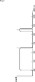
- FIG. 2 shows the transmission characteristics of the IR bandpass filter 12.
- the IR bandpass filter 12 has high transmittance for visible light having a wavelength of 400 nm to 650 nm and infrared light having a peak at a wavelength of 850 nm (infrared light irradiated by the irradiation system).
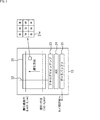
- FIG. 3 shows a configuration example of the CMOS image sensor 13.
- the CMOS image sensor 13 includes a sensor array 21, a signal line 22, an analog gain amplifier 23, an ADC 24, and a data buffer 25.
- the sensor array 21 is composed of photoelectric conversion elements for each pixel arranged vertically and horizontally, and the light receiving surface side is covered with a color filter 21a such as a Bayer array.
- FIG. 4 shows the exposure with each pixel time in the sensor array 21 of the CMOS image sensor 13 and the readout timing of the charge signal obtained thereby.
- the exposure period is shifted in units of lines in accordance with the sweep direction from the sweep start line (1st-Line) to the last line (Last-Lien), and the exposure period is completed.
- the charge signals obtained during the timing are read out collectively for each row.
- different exposure times are set for each color, and when infrared light is irradiated, for example, red pixels are not exposed, and white pixels are Control such as exposure is performed.
- the read charge signal is output to the analog gain amplifier 23 via the signal line 22 and amplified, converted into a digital pixel signal by the ADC 24 and stored in the data buffer 25.
- the gain in the analog gain amplifier 23 can be set adaptively according to the illumination.
- pixel signals for all the pixels constituting the sensor array 21 are output as image signals to the subsequent image processing system.
- the image signal at this stage is RAW data in which each pixel has color information of any one of R, G, and B.
- RAW data including W (white) color information can also be used.
- description will be continued by taking as an example a case where RGBW color information is handled.
- the image processing system of the imaging apparatus 10 includes a camera DSP unit 14 and memories 15 and 16.
- the camera DSP unit 14 generates a color image in which each pixel has color information of R, G, B, and W based on the image signal from the imaging system.
- the memories 15 and 16 temporarily hold image signals used for NR (noise reduction) processing.
- the camera DSP unit 14 generates and outputs a V synchronization signal for controlling driving (exposure and reading) of the CMOS image sensor 13 of the imaging system.
- the camera DSP unit 14 generates and outputs a driver signal (ON / OFF signal and intensity adjustment signal) for controlling the irradiation system.
- the irradiation system of the imaging apparatus 10 includes an IR driving unit 17 and an IR irradiation unit 18.
- the IR drive unit 17 irradiates infrared light from the IR irradiation unit 18 in accordance with control from the camera DSP unit 14.
- the IR irradiation unit 18 irradiates infrared light having a peak at a wavelength of 850 nm toward the imaging range.
- the IR irradiation unit 18 may be disposed inside the housing of the imaging device 10 or may be disposed outside the housing of the imaging device 10.
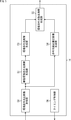
- FIG. 5 shows a configuration example of the camera DSP unit 14.
- the camera DSP unit 14 includes an environment infrared light including image acquisition unit 51, a discrete environment infrared light image generation unit 52, an environment infrared light image generation unit 53, an infrared light pixel correction image generation unit 54, and an environment infrared light removal.
- the image generation unit 55 and the timing control unit 56 are included.
- An image captured by the CMOS image sensor 13 is processed.
- the timing control unit 56 generates and outputs a V synchronization signal for controlling driving (exposure and reading) of the CMOS image sensor 13 of the imaging system, and a driver signal (ON / OFF signal for controlling the light projecting system). And intensity adjustment signal).
- the environmental infrared light-containing image acquisition unit 51 acquires an image signal from the CMOS image sensor 13.
- Each of the R pixel, the G pixel, the B pixel, and the W pixel receives infrared light as well as visible light, and generates a pixel signal including one color signal from the light. Therefore, the color signals of these pixels include a visible light component that is a signal photoelectrically converted from visible light and an infrared light component that is a signal photoelectrically converted from infrared light. That is, the CMOS image sensor 13 captures an image including infrared light included in the environment.
- IR included in such an environment is described as ambient infrared light.
- the environmental infrared light-containing image acquisition unit 51 acquires an image signal of an environmental infrared light-containing image including a visible light component and an environmental infrared light component.
- the acquired environment infrared light-containing image is supplied to the discrete environment infrared light image generation unit 52 and the infrared light pixel correction image generation unit 54.
- the discrete environment infrared light image generation unit 52 extracts infrared light pixels from the image including the environment infrared light.
- the infrared light pixel is a pixel arranged in the sensor array 21 like the R pixel, and is a pixel that receives environmental infrared light. With reference to FIG. 6, a description will be given of the pixels arranged in the sensor array 21.
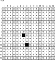
- R pixels, G pixels, B pixels, W pixels, and infrared light pixels are arranged.
- a pixel indicated as R is an R pixel
- a pixel indicated as G is a G pixel
- a pixel indicated as B is a B pixel
- the black squares are infrared light pixels.
- the R pixel, G pixel, B pixel, and W pixel are regularly arranged.
- the first row is a rule that repeats in the order of R pixel, W pixel, B pixel, and W pixel
- the second row is W pixel
- the W pixel functions as a spectral sensitivity pixel having total color matching, and the R pixel, the G pixel, and the B pixel function as spectral sensitivity pixels having characteristics in the respective colors.
- R pixels, G pixels, B pixels, and W pixels are regularly arranged, whereas infrared light pixels are irregularly arranged.
- the pixel in the 9th row and the 7th column and the pixel in the 12th row and the 8th column are set as infrared light pixels.
- the infrared light pixels are arranged at random, the generation of noise can be suppressed and the image quality can be improved, but later signal processing may be complicated. As will be described later, the infrared light pixels may be regularly arranged. When the infrared light pixels are regularly arranged, noise may be generated, but later signal processing can be performed relatively easily.
- the infrared light pixels are randomly or regularly arranged in the sensor array 21. Whether the arrangement is random or regular may be set depending on the desired image quality and signal processing capability. Further, it may be randomly arranged with a certain degree of regularity. For example, 8 ⁇ 8 pixels are defined as one unit, and one infrared light pixel is arranged within one unit, and the positions of the infrared light pixels arranged within one unit are random.
- the number of infrared light pixels arranged in the sensor array 21 may be set according to image quality and signal processing capability.
- the discrete environment infrared light image generation unit 52 extracts the infrared light pixels arranged discretely from the image including the environment infrared light, and generates a discrete environment infrared light image.
- the processing performed in the camera DSP unit 14 will be described with reference to FIG.
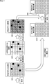
- the environment infrared light-containing image 101 is acquired by the environment infrared light-containing image acquisition unit 51 and supplied to the discrete environment infrared light image generation unit 52 and the infrared light pixel correction image generation unit 54.
- the discrete environment infrared light image generation unit 52 generates a discrete environment infrared light image 102 by extracting infrared light pixels from the environment infrared light-containing image 101.
- the discrete environment infrared light image 102 is an image having pixel values only in the infrared light image.
- the infrared pixel receives ambient infrared light and outputs a pixel value corresponding to the intensity.
- the discrete environment infrared light image 102 is an image including pixel values of infrared light pixels that are discretely arranged.
- the discrete environment infrared light image 102 generated by the discrete environment infrared light image generation unit 52 is supplied to the environment infrared light image generation unit 53 (FIG. 5).
- the ambient infrared light image generation unit 53 uses pixel values obtained from the infrared light pixels for pixels that are not infrared light pixels, in other words, R pixel, G pixel, B pixel, and W pixel portions. Thus, pixel values corresponding to the respective pixels are generated.
- the environmental infrared light image generation unit 53 generates an image (environmental infrared light image 103) obtained when all pixels in one image are infrared light pixels, and generates an environmental infrared light removal image. It supplies to the part 55 (FIG. 5).
- the infrared light pixel correction image generation unit 54 executes processing for returning the infrared light pixel to the pixel value of the original color pixel.
- FIG. 6 again.
- the pixel in the 9th row and the 7th column and the pixel in the 12th row and the 8th column are set as infrared light pixels.
- the pixel in the ninth row and the seventh column is the B pixel. That is, the pixel in the 9th row and the 7th column is originally a B pixel.
- the infrared light pixel correction image generation unit 54 obtains the pixel value from the 9th row and 7th column infrared light pixel if the 9th row and 7th column pixel is a B pixel. Generate and replace values. Other infrared light pixel portions are also replaced with pixel values obtained in the case of original color pixels.
- the infrared light pixel correction image generation unit 54 includes only the pixel values of the R pixel, the G pixel, the B pixel, and the W pixel (not including the pixel value of the infrared light pixel). (FIG. 7) is generated and supplied to the environmental infrared light removal image generation unit 55.
- the environmental infrared light removal image generation unit 55 is supplied with the environmental infrared light image 103 from the environmental infrared light image generation unit 53 and the infrared light pixel correction image 104 from the infrared light pixel correction image generation unit 54.
- the environmental infrared light image 103 is an image composed of environmental infrared light components.
- the infrared light pixel corrected image 104 is an image including a visible light component and an environmental infrared light component.
- the environmental infrared light removal image generation unit 55 subtracts the environmental infrared light image 103 including the environmental infrared light component from the infrared light pixel corrected image 104 including the visible light component and the environmental infrared light component. Then, an environment infrared light removed image 105 (FIG. 7) composed of a visible light component from which the environment infrared light component has been removed is generated.
- the camera DSP unit 14 executes processing for generating an image from which environmental infrared light is removed.
- the processing in the camera DSP unit 14 may include processing for reducing noise.
- the environmental infrared light-containing image acquisition unit 51 performs a process (noise reduction) for reducing noise on the environmental infrared light-containing image 101.
- the later environment infrared light-containing image 101 may be supplied to the discrete environment infrared light image generation unit 52 and the infrared light pixel correction image generation unit 54.
- demosaic processing may be executed. For example, in the process of obtaining information on G pixels, B pixels, and W pixels in R pixels, pixels obtained from an image sensor that has been covered with an R (red) filter include G pixels, B pixels, and W pixels. Since there is no information, it is calculated from the pixel information of the G pixel, B pixel, and W pixel close to the R pixel and complemented. Such processing is called demosaic processing.
- the demosaic processing is executed by the discrete environment infrared light image generation unit 52 and the environment infrared light image generation unit 53 (FIG. 5) for the infrared light pixels.
- the pixel value at the pixel position that is not the infrared light pixel is calculated from the pixel value of the infrared light pixel, and interpolation processing is performed so that the intensity of the environmental infrared light is reduced in all the pixels in one image.
- An ambient infrared light image 103 in which the indicated pixel value is interpolated is generated.
- the demosaic process is performed on each of the R pixel, the G pixel, the B pixel, and the W pixel, for example, before or after the infrared light pixel correction image 104 is generated by the infrared light pixel correction image generation unit 54.
- the infrared light pixel correction image generation unit 54 performs an R image consisting only of R pixel values, a G image consisting only of G pixel values, and a B image consisting only of B pixel values.
- a W image including only the pixel value of the W pixel may be generated and supplied to the ambient infrared light removal image generation unit 55.
- the environment infrared light removed image generation unit 55 the environment infrared light is subtracted from each of the R image, the G image, the B image, and the W image, thereby removing the environment infrared light.
- G image, B image, and W image may be generated.
- the environment infrared light removed image 105 is generated by subtracting the environment infrared light image 103 from the infrared light pixel correction image 104 by the environment infrared light removed image generation unit 55, and then the demosaic process is executed. Then, an R image, a G image, a B image, and a W image may be generated.
- an image sensor such as a CMOS image sensor 13 has sensitivity in a wavelength region of about 400 nm to 1000 nm, and makes light from a subject incident as it is. The image becomes reddish depending on the sensitivity to the wavelength component (about 700 nm to 1000 nm) in the infrared region.
- the camera DSP unit 14 removes the ambient infrared light as described above, so that the same color reproducibility as that seen by human eyes can be realized.
- the imaging device 10 includes the IR irradiating unit 18 and irradiates infrared light, and images reflected light of the irradiated infrared light to improve sensitivity. It is configured as follows. However, if the infrared light is simply irradiated, the reflected infrared light reflected by the subject is received, and color information such as R, G, and B cannot be obtained, and the reflected light is reflected. Only the received light intensity of (infrared light) can be acquired. Therefore, the obtained image becomes a monochrome image such as gray or green.
- the imaging apparatus 10 to which the present technology is applied in order to obtain a color image even when imaging is performed using infrared light when the visible light is low and dark, such as at night, is shown in FIG.
- the irradiation of infrared light and exposure are controlled.
- the upper row shows exposure of infrared light pixels, R pixels, G pixels, and B pixels, and the lower row shows exposure of W pixels.
- the IR irradiation unit 18 starts irradiation with infrared light.
- infrared irradiation is started by the IR irradiation unit 18.
- the infrared irradiation by the IR irradiation unit 18 is stopped.
- exposure of the infrared light pixel, R pixel, G pixel, and B pixel in the first line is started.
- the exposure of the infrared light pixel, R pixel, G pixel, and B pixel in the final line is started.
- the exposure of the infrared light pixel, R pixel, G pixel, B pixel, and W pixel in the first line is completed.
- the exposure of the infrared light pixel, the R pixel, the G pixel, the B pixel, and the W pixel in the final line is finished.
- the infrared light is irradiated only from time t2 to time t3, and is not irradiated at other times.
- the W pixel is maintained in an exposed state.
- the infrared light pixel, the R pixel, the G pixel, and the B pixel are kept exposed from time t3 to time t5.
- infrared light irradiation is performed only while the W pixel is exposed, and is not performed while the infrared light pixel, the R pixel, the G pixel, and the B pixel are exposed. Therefore, since the W pixel receives reflected light due to irradiation with infrared light, imaging with sufficient luminance can be performed.
- the infrared light pixel captures an image when it is not irradiated with infrared light, it can capture only the infrared light present in the environment without being affected by the irradiation of infrared light. it can. Since the R pixel, the G pixel, and the B pixel perform imaging when infrared light irradiation is not performed, the subject can be imaged without being affected by the infrared light irradiation.
- a color image can be generated from images captured with R, G, and B pixels. Even if the image is captured when the amount of visible light is low and dark, such as at night, the reproducibility of luminance can be ensured with the image captured with the W pixel. Therefore, by using the image captured with the W pixel, R It is possible to correct the luminance of a color image generated from an image picked up by pixels, G pixels, and B pixels.
- the low frequency components of the color information and the luminance information are generated from pixels (such as R pixels) that do not receive the irradiated infrared light, and pixels that receive the irradiated infrared light.
- a high frequency component of luminance information can be generated from (W pixel).
- the color image can be an image with good image quality.
- the irradiation with infrared light may be performed only when the visible light is low and dark as in the night, or may be performed when the light is bright as in the daytime.
- the irradiation with infrared light may be performed only when the visible light is low and dark as in the night, or may be performed when the light is bright as in the daytime.
- the exposure time of each pixel may be made uniform.
- the exposure time for the R pixel, the G pixel, and the B pixel may be set longer than the exposure time for the W pixel in consideration of the sensitivity difference.
- step S11 the timing control unit 56 generates a signal for starting exposure of the W pixel and supplies the signal to the CMOS image sensor 13.
- step S12 the timing control unit 56 instructs the IR drive unit 17 (FIG. 1) to start infrared light irradiation (outputs an ON signal) to start infrared light irradiation. .
- step S13 the timing control unit 56 instructs the IR drive unit 17 (FIG. 1) to stop the infrared light irradiation (outputs an OFF signal) in order to stop the infrared light irradiation.
- step S ⁇ b> 14 the timing control unit 56 generates a signal for starting exposure of the infrared light pixel, the R pixel, the G pixel, and the B pixel (other than the W pixel), and supplies the signal to the CMOS image sensor 13.
- step S ⁇ b> 15 the timing control unit 56 generates a signal for stopping the exposure of the infrared light pixel, the R pixel, the G pixel, the B pixel, and the W pixel (all pixels), and supplies the signal to the CMOS image sensor 13. .
- step S11 is executed at time t1 (FIG. 8)
- the process in step S12 is executed at time t2 (FIG. 8)
- the process in step S13 is executed at time t3 (FIG. 8).
- the process in step S14 is executed at time t3 (FIG. 8)
- the process in step S15 is executed at time t5 (FIG. 8).
- step S ⁇ b> 16 the environmental infrared light including image acquisition unit 51 acquires the environmental infrared light including image 101 from the CMOS image sensor 13.
- the acquired environment infrared light-containing image 101 is supplied to the discrete environment infrared light image generation unit 52 and the infrared light pixel correction image generation unit 54.
- step S ⁇ b> 17 the discrete environment infrared light image generation unit 52 extracts infrared light pixels from the supplied environment infrared light embedded image 101 to generate a discrete environment infrared light image 102.
- the generated discrete environment infrared light image 102 is supplied to the environment infrared light image generation unit 53.
- step S ⁇ b> 18 the environment infrared light image generation unit 53 uses the supplied discrete environment infrared light image 102 to calculate a pixel value at a pixel position that is not an infrared light pixel, and perform an interpolation process to obtain 1
- An environmental infrared light image 103 in which pixel values indicating the intensity of the environmental infrared light are interpolated is generated for all the pixels in the image.
- the generated environment infrared light image 103 is supplied to the environment infrared light removal image generation unit 55.
- step S ⁇ b> 19 the infrared light pixel correction image generation unit 54 interpolates the pixel values of the pixels corresponding to the infrared pixels in the supplied environment infrared light-containing image 101 using the pixel values of adjacent pixels. Then, the pixel value corresponding to the R pixel, G pixel, B pixel, or W pixel is corrected.
- the infrared light pixel corrected image 104 in which the pixel value of the infrared pixel is corrected is supplied to the environmental infrared light removal image generation unit 55.
- step S ⁇ b> 20 the environmental infrared light removal image generation unit 55 subtracts the environmental infrared light image 103 from the supplied infrared light pixel correction image 104 to thereby remove the environmental infrared light from which the environmental infrared light has been removed.
- a removal image 105 is generated and output to a subsequent processing unit (not shown).
- Such processing is performed by the camera DSP unit 14. Note that a noise reduction process or a demosaic process may be included between these processes.
- FIG. 10 shows another arrangement example of the infrared light pixel.
- the arrangement of the infrared light pixels described with reference to FIG. 6 is an example of irregular arrangement, but the arrangement of the infrared light pixels shown in FIG. 10 is an example of regular arrangement. It is.
- the infrared light pixels shown in FIG. 10 are arranged in even rows and even columns.
- infrared light pixels are arranged in the second, second, sixth, tenth, and fourteenth rows, respectively.
- infrared pixels are arranged in the fourth row, the fourth column, the eighth column, the twelfth column, and the sixteenth column, respectively.
- the infrared light pixel shown in FIG. 10 is disposed at a position where the G pixel is disposed. More G pixels are arranged than R pixels and B pixels. Some of the many G pixels arranged may be infrared light pixels.
- the infrared light pixels may be regularly arranged on the sensor array 21 (FIG. 3).
- signal processing for example, processing such as interpolation of pixel values when the environmental infrared light image 103 is generated by the environmental infrared light image generation unit 53 is performed.
- processing such as interpolation of pixel values when the environmental infrared light image 103 is generated by the environmental infrared light image generation unit 53 is performed.
- the infrared light pixels are randomly arranged, it can be reduced.
- FIG. 11 is a diagram showing still another arrangement example of the infrared light pixels.
- the hatched pixels correspond to infrared light pixels.
- the infrared light pixels are regularly arranged as in the arrangement example shown in FIG. 10.
- the arrangement example of the infrared light pixels shown in FIG. 11 is an example in which, in the RGBW pixel array, pixels corresponding to half of the W pixels are infrared light pixels.
- two types of W pixels are arranged. One is a W pixel that receives irradiated infrared light, and the other does not receive irradiated infrared light. W pixel.
- the W pixel that does not receive the irradiated infrared light functions as an infrared light pixel that receives the ambient infrared light.
- the exposure of pixels that are W pixels that do not receive irradiated infrared light and function as infrared light pixels is controlled in the same manner as the exposure of infrared light pixels shown in FIG. That is, the exposure of the W pixel (infrared light pixel) that does not receive the irradiated infrared light is started from the time t3 when the irradiation of the infrared light is stopped.
- the infrared light pixels may be regularly arranged on the sensor array 21 (FIG. 3). Further, some of the W pixels arranged in the sensor array 21 are pixels that do not receive the irradiated infrared light, and may function as infrared light pixels.
- some W pixels are set as infrared light pixels, but the infrared light pixels may be arranged at random.
- the W pixels themselves are regularly arranged, but the pixels set as infrared light pixels among them are not necessarily arranged regularly.
- the address of the pixel set to the infrared light pixel is managed, and the pixel corresponding to the managed address is not exposed when the infrared light is irradiated.
- the number of pixels set in the infrared light pixel may be changed according to the brightness of the shooting environment. For example, when shooting is performed in a bright environment, environmental infrared light has a strong effect on image quality. Therefore, the number of pixels that function as infrared light pixels is increased, and when shooting is performed in a dark environment, environmental infrared light is used. Since the influence on the image quality is weak, the number of pixels that function as infrared light pixels may be reduced, and the number of W pixels may be increased correspondingly to perform shooting that improves the SN ratio.
- the pixels set as infrared light pixels may be changed as appropriate. It determines which pixel in the sensor array 21 is set as an infrared light pixel according to the photographing environment and the like, and the determined pixel is controlled not to be exposed while the infrared light is irradiated. You may make it.
- the address may be stored in the static defective pixel correction circuit, and a process such as correction may be performed. Since the static defective pixel correction circuit is often provided in an imaging apparatus, the circuit scale can be increased even when an infrared light pixel is provided by using such a static defective pixel correction circuit. It becomes possible to suppress the increase in size and the complexity of the processing.
- the management of the infrared light pixels by the address can be applied to all the above-described embodiments. For example, in the case where the infrared light pixels are discretely arranged as shown in FIG. It is possible to manage the positions of the infrared light images arranged discretely by using an address so that control such as exposure is performed.
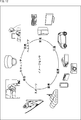
- FIG. 12 is a diagram illustrating a usage example of the above-described imaging device.
- the imaging device described above can be used in various cases for sensing light such as visible light, infrared light, ultraviolet light, and X-rays as follows.
- Devices for taking images for viewing such as digital cameras and mobile devices with camera functions
- Devices used for traffic such as in-vehicle sensors that capture the back, surroundings, and interiors of vehicles, surveillance cameras that monitor traveling vehicles and roads, and ranging sensors that measure distances between vehicles, etc.
- Equipment used for home appliances such as TVs, refrigerators, air conditioners, etc. to take pictures and operate the equipment according to the gestures ⁇ Endoscopes, equipment that performs blood vessel photography by receiving infrared light, etc.
- Equipment used for medical and health care ⁇ Security equipment such as security surveillance cameras and personal authentication cameras ⁇ Skin measuring instrument for photographing skin and scalp photography Such as a microscope to do beauty Equipment used for sports, such as action cameras and wearable cameras for sports applications, etc.
- Equipment used for agriculture such as cameras for monitoring the condition of fields and crops
- the series of processes described above can be executed by hardware or can be executed by software.
- a program constituting the software is installed in the computer.
- the computer includes, for example, a general-purpose personal computer capable of executing various functions by installing various programs by installing a computer incorporated in dedicated hardware.
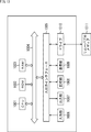
- FIG. 13 is a block diagram showing an example of the hardware configuration of a computer that executes the above-described series of processing by a program.
- a CPU Central Processing Unit
- ROM Read Only Memory
- RAM Random Access Memory
- An input / output interface 1005 is further connected to the bus 1004.
- An input unit 1006, an output unit 1007, a storage unit 1008, a communication unit 1009, and a drive 1010 are connected to the input / output interface 1005.
- the input unit 1006 includes a keyboard, a mouse, a microphone, and the like.
- the output unit 1007 includes a display, a speaker, and the like.
- the storage unit 1008 includes a hard disk, a nonvolatile memory, and the like.
- the communication unit 1009 includes a network interface.
- the drive 1010 drives a removable medium 1011 such as a magnetic disk, an optical disk, a magneto-optical disk, or a semiconductor memory.
- the CPU 1001 loads, for example, the program stored in the storage unit 1008 to the RAM 1003 via the input / output interface 1005 and the bus 1004 and executes the program. Is performed.
- the program executed by the computer (CPU 1001) can be provided by being recorded on the removable medium 1011 as a package medium, for example.
- the program can be provided via a wired or wireless transmission medium such as a local area network, the Internet, or digital satellite broadcasting.
- the program can be installed in the storage unit 1008 via the input / output interface 1005 by attaching the removable medium 1011 to the drive 1010. Further, the program can be received by the communication unit 1009 via a wired or wireless transmission medium and installed in the storage unit 1008. In addition, the program can be installed in advance in the ROM 1002 or the storage unit 1008.
- the program executed by the computer may be a program that is processed in time series in the order described in this specification, or in parallel or at a necessary timing such as when a call is made. It may be a program for processing.
- system represents the entire apparatus composed of a plurality of apparatuses.
- An infrared light irradiation unit for irradiating infrared light A first pixel that includes a period during which the infrared light is irradiated by the infrared light irradiation unit as an exposure time, a second pixel that does not include a period during which the infrared light is irradiated as an exposure time, and the environment
- An acquisition unit that acquires an infrared light image captured by the first pixel, a visible image captured by the second pixel, and an environmental infrared light image captured by the infrared light pixel;
- An imaging apparatus comprising: an image generation unit configured to generate an image obtained by removing infrared light included in environmental light from the infrared light image and the visible image using the environmental infrared light image.
- the imaging device (2) The imaging device according to (1), wherein the first pixel is a pixel having spectral sensitivity that has total color matching, and the second pixel is a pixel having spectral sensitivity that has a characteristic of a predetermined color.
- the infrared light pixel is subjected to the same exposure control as that of the second pixel.
- the infrared light pixels are discretely arranged in the sensor array.
- the address of the infrared light pixel is stored by a static defective pixel correction circuit, and the correction is performed by the static defective pixel correction circuit.
- the imaging apparatus according to (8). (10) Irradiate infrared light, A first pixel that includes a period in which the infrared light is irradiated as an exposure time; a second pixel that does not include the period in which the infrared light is irradiated as an exposure time; An infrared light image captured by the first pixel, a visible image captured by the second pixel, and the red Acquire an ambient infrared light image captured by external light pixels, An imaging method including a step of generating, from the infrared light image and the visible image, an image obtained by removing infrared light included in environmental light using the environmental infrared light image.
- Irradiate infrared light A first pixel that includes a period in which the infrared light is irradiated as an exposure time; a second pixel that does not include the period in which the infrared light is irradiated as an exposure time; An infrared light image captured by the first pixel, a visible image captured by the second pixel, and the red Acquire an ambient infrared light image captured by external light pixels,
- a program for causing a computer to execute processing including a step of generating an image in which infrared light included in environmental light is removed from the infrared light image and the visible image using the environmental infrared light image.
Landscapes
- Engineering & Computer Science (AREA)
- Multimedia (AREA)
- Signal Processing (AREA)
- Physics & Mathematics (AREA)
- Spectroscopy & Molecular Physics (AREA)
- General Physics & Mathematics (AREA)
- Studio Devices (AREA)
- Color Television Image Signal Generators (AREA)
- Transforming Light Signals Into Electric Signals (AREA)
Abstract
本技術は、暗いところを撮影した場合でもカラー画像を得られるようにすることができるようにする撮像装置、撮像方法、およびプログラムに関する。 赤外光を照射する赤外光照射部と、赤外光照射部により赤外光が照射されている期間を露光時間に含む第1の画素、赤外光が照射されている期間を露光時間に含まない第2の画素、および環境光に含まれる赤外光を受光する赤外光画素を含む複数の画素が配置されているセンサアレイと、第1の画素で撮像された赤外光画像、第2の画素で撮像された可視画像、および赤外光画素で撮像された環境赤外光画像を取得する取得部と、赤外光画像と可視画像から、環境赤外光画像を用いて、環境光に含まれる赤外光を除去した画像を生成する画像生成部とを備える。本技術は、例えば監視カメラに適用できる。
Description
本技術は、撮像装置、撮像方法、およびプログラムに関する。詳しくは、赤外光を照射して撮像した赤外画像を用いた場合においても、カラー画像を生成できるようにし、画質を向上させた撮像を行えるようにした撮像装置、撮像方法、およびプログラムに関する。
従来、例えば監視カメラには、日中の自然光下や白色光などの可視光の照明下で撮像を行うデイモードと、赤外光を照射して撮像を行うナイトモードの二種類のモードを備えているものがある。
デイモードの撮像ではカラー画像を得ることができる。一方、ナイトモードの撮像では、照射した赤外光が被写体で反射した反射光を受光することになるので、R,B,Gなどの色情報を得ることができず、反射光(赤外光)の受光強度のみを取得できる。よって、得られる画像はグレーやグリーンなどのモノクロ画像となる。
しかしながらナイトモードの撮像であってもカラー画像を得られることが望ましい。そこで従来、撮像範囲(被写体)に赤外光を照射した状態を撮像して得られる画像(以下、赤外画像と称する)に基づいてカラー画像を生成する様々な手法が提案されている。
例えば、特許文献1には、赤外光を照射した状態の赤外画像と、赤外光を照射していない低照度下での可視画像を連続して撮像し、これらを用いてカラー画像を生成する技術が開示されている。
特許文献1においては、赤外光を照射した状態の赤外画像と、赤外光を照射していない低照度下での可視画像を連続して撮像するため、出力されるフレームレートは、撮影したフレームレートに対して、1/2程度となってしまう。フレームレートを落とすことなく、またナイトモードの撮像であってもカラー画像が得られるようにすることが望まれている。
本技術は、このような状況に鑑みてなされたものであり、赤外光を用いた場合であっても、カラー画像を得られるようにし、画質を向上させた画像を撮像できるようにするものである。
本技術の一側面の撮像装置は、赤外光を照射する赤外光照射部と、前記赤外光照射部により前記赤外光が照射されている期間を露光時間に含む第1の画素、前記赤外光が照射されている期間を露光時間に含まない第2の画素、および環境光に含まれる赤外光を受光する赤外光画素を含む複数の画素が配置されているセンサアレイと、前記第1の画素で撮像された赤外光画像、前記第2の画素で撮像された可視画像、および前記赤外光画素で撮像された環境赤外光画像を取得する取得部と、前記赤外光画像と前記可視画像から、前記環境赤外光画像を用いて、環境光に含まれる赤外光を除去した画像を生成する画像生成部とを備える。
前記第1の画素は、全整色性である分光感度の画素であり、前記第2の画素は、所定の色に特性のある分光感度の画素であるようにすることができる。
前記赤外光画素は、前記第2の画素と同じ露光制御がされるようにすることができる。
前記赤外光画素は、前記センサアレイ内で離散的に配置されているようにすることができる。
前記赤外光画素は、前記センサアレイ内で規則的に配置されているようにすることができる。
前記第1の画素の一部が、前記赤外光画素であるようにすることができる。
前記赤外光画素の位置は、アドレスで管理されているようにすることができる。
前記赤外光画素が、前記第1の画素または前記第2の画素であった場合の画素値に補正し、補正後の前記赤外光画像と前記可視画像から、前記環境赤外光画像が減算されることで、前記環境光に含まれる赤外光が除去された画像が生成されるようにすることができる。
前記赤外光画素は、スタティック欠陥画素補正回路にてアドレスが記憶され、前記補正は、前記スタティック欠陥画素補正回路で行われるようにすることができる。
本技術の一側面の撮像方法は、赤外光を照射し、前記赤外光が照射されている期間を露光時間に含む第1の画素、前記赤外光が照射されている期間を露光時間に含まない第2の画素、および環境光に含まれる赤外光を受光する赤外光画素を含む複数の画素が配置されているセンサアレイから、前記第1の画素で撮像された赤外光画像、前記第2の画素で撮像された可視画像、および前記赤外光画素で撮像された環境赤外光画像を取得し、前記赤外光画像と前記可視画像から、前記環境赤外光画像を用いて、環境光に含まれる赤外光を除去した画像を生成するステップを含む。
本技術の一側面のプログラムは、赤外光を照射し、前記赤外光が照射されている期間を露光時間に含む第1の画素、前記赤外光が照射されている期間を露光時間に含まない第2の画素、および環境光に含まれる赤外光を受光する赤外光画素を含む複数の画素が配置されているセンサアレイから、前記第1の画素で撮像された赤外光画像、前記第2の画素で撮像された可視画像、および前記赤外光画素で撮像された環境赤外光画像を取得し、前記赤外光画像と前記可視画像から、前記環境赤外光画像を用いて、環境光に含まれる赤外光を除去した画像を生成するステップを含む処理をコンピュータに実行させるためのプログラムである。
本技術の一側面の撮像装置、撮像方法、およびプログラムにおいては、赤外光が照射され、赤外光が照射されている期間を露光時間に含む第1の画素、赤外光が照射されている期間を露光時間に含まない第2の画素、および環境光に含まれる赤外光を受光する赤外光画素を含む複数の画素が配置されているセンサアレイから、第1の画素で撮像された赤外光画像、第2の画素で撮像された可視画像、および赤外光画素で撮像された環境赤外光画像が取得され、赤外光画像と可視画像から、環境赤外光画像が用いられて、環境光に含まれる赤外光が除去された画像が生成される。
本技術の一側面によれば、赤外光を用いた場合であっても、カラー画像を得られ、画質を向上させた画像を撮像できるようになる。
なお、ここに記載された効果は必ずしも限定されるものではなく、本開示中に記載されたいずれかの効果であってもよい。
以下に、本技術を実施するための形態(以下、実施の形態という)について説明する。なお、説明は、以下の順序で行う。
1.撮像装置の構成
2.カメラDSP部の構成
3.赤外光の照射について
4.カメラDSP部の処理
5.赤外光画素の他の配置
6.撮像装置の使用例
7.記録媒体について
1.撮像装置の構成
2.カメラDSP部の構成
3.赤外光の照射について
4.カメラDSP部の処理
5.赤外光画素の他の配置
6.撮像装置の使用例
7.記録媒体について
<撮像装置の構成>
図1は、本開示の実施の形態である撮像装置の構成例を示している。
図1は、本開示の実施の形態である撮像装置の構成例を示している。
この撮像装置10は、例えば監視カメラなどに用いられるものであり、赤外光を照射した状態で得られる赤外画像と、赤外光を照射していない低照度下で得られる可視画像に基づいてカラー画像を生成するものである。
撮像装置10は、一般的なカメラと同様に構成される撮像系と、画像処理を実施する画像処理系と、撮像範囲に向けて赤外光を照射する照射系から構成される。
撮像装置10の撮像系は、レンズ11、IRバンドパスフィルタ12、および、フォーカルプレーン読み出し方式(ローリングシャッタ方式)のCMOSイメージセンサ13から成る。撮像系においては、レンズ11が被写体の光学像をCMOSイメージセンサ13に集光し、レンズ11とCMOSイメージセンサ13の間に配置されたIRバンドパスフィルタ12が被写体の光学像から可視光成分および赤外光成分を抽出し、CMOSイメージセンサ13が入射光に基づく画像信号を生成して画像処理系に出力する。
図2は、IRバンドパスフィルタ12の透過特性を示している。IRバンドパスフィルタ12は、波長400nmから650nmの可視光と、波長850nmにピークをもつ赤外光(照射系が照射する赤外光)に対して高い透過率を有するものとする。
図3は、CMOSイメージセンサ13の構成例を示している。このCMOSイメージセンサ13は、センサアレイ21、信号線22、アナログゲインアンプ23、ADC24、およびデータバッファ25を有する。センサアレイ21は、縦横に配置された画素毎の光電変換素子からなり、その受光面側はベイヤ配列などのカラーフィルタ21aで覆われている。
図4は、CMOSイメージセンサ13のセンサアレイ21における各画素時間との露光とそれによって得られる電荷信号の読み出しタイミングを示している。図示するように、CMOSイメージセンサ13においては、掃引開始行(1st-Line)から最終行(Last-Lien)に向かう掃引方向に従い、行単位で露光期間がずらされており、露光期間が終了したタイミングでその間に得られた電荷信号が行毎に一括して読み出される。
なお、後述するように、本実施の形態においては、色毎に異なる露光時間が設定されており、赤外光が照射されているときには、例えば赤色の画素は、露光せず、白色の画素は露光するといった制御がなされる。
読み出された電荷信号は信号線22を介してアナログゲインアンプ23に出力されて増幅され、ADC24でデジタルの画素信号に変換されてデータバッファ25に格納される。なお、アナログゲインアンプ23におけるゲインは照明に応じて適応的に設定することが可能である。そして、センサアレイ21を構成する全画素分の画素信号が画像信号として後段の画像処理系に出力される。なお、この段階における画像信号は、各画素がR,G,Bのいずれかの色情報を有するRAWデータである。なお、W(白色)の色情報も含むRAWデータとすることもできる。以下、RGBWの色情報が扱われる場合を例に挙げて説明を続ける。
図1に戻る。撮像装置10の画像処理系は、カメラDSP部14、およびメモリ15,16から成る。画像処理系においては、カメラDSP部14が撮像系からの画像信号に基づいて、各画素のそれぞれがR,G,B,Wの色情報を有するカラー画像を生成する。メモリ15,16には、NR(ノイズリダクション)処理のために用いる画像信号が一時的に保持される。また、カメラDSP部14は撮像系のCMOSイメージセンサ13の駆動(露光や読み出し)を制御するためのV同期信号を発生、出力する。さらに、また、カメラDSP部14は照射系を制御するためのドライバ信号(ON/OFF信号および強度調整信号)を発生、出力する。
撮像装置10の照射系は、IR駆動部17およびIR照射部18から成る。照射系においては、カメラDSP部14からの制御に従い、IR駆動部17がIR照射部18から赤外光を照射させる。IR照射部18は波長850nmにピークをもつ赤外光を撮像範囲に向けて照射する。なお、IR照射部18は撮像装置10の筐体内に配置してもよいし、撮像装置10の筐体外部に配置してもよい。
<カメラDSP部の構成>
図5は、カメラDSP部14の構成例を示している。カメラDSP部14は、環境赤外光込画像取得部51、離散環境赤外光画像生成部52、環境赤外光画像生成部53、赤外光画素補正画像生成部54、環境赤外光除去画像生成部55、およびタイミング制御部56を含む構成とされている。
図5は、カメラDSP部14の構成例を示している。カメラDSP部14は、環境赤外光込画像取得部51、離散環境赤外光画像生成部52、環境赤外光画像生成部53、赤外光画素補正画像生成部54、環境赤外光除去画像生成部55、およびタイミング制御部56を含む構成とされている。
環境赤外光込画像取得部51、離散環境赤外光画像生成部52、環境赤外光画像生成部53、赤外光画素補正画像生成部54、環境赤外光除去画像生成部55は、CMOSイメージセンサ13で撮像された画像を処理する。
タイミング制御部56は、撮像系のCMOSイメージセンサ13の駆動(露光や読み出し)を制御するためのV同期信号を発生、出力したり、投光系を制御するためのドライバ信号(ON/OFF信号および強度調整信号)を発生、出力したりする。
環境赤外光込画像取得部51は、CMOSイメージセンサ13からの画像信号を取得する。R画素、G画素、B画素およびW画素のそれぞれは、可視光とともに赤外光を受光して、それらの光から、1つの色信号を含む画素信号を生成する。このため、これらの画素の色信号は、可視光から光電変換された信号である可視光成分と、赤外光から光電変換された信号である赤外光成分とを含む。すなわち、CMOSイメージセンサ13は、環境に含まれる赤外光も含んで撮像している。ここでは、このような環境に含まれるIRを環境赤外光と記述する。
環境赤外光込画像取得部51は、可視光成分と環境赤外光成分を含む環境赤外光込画像の画像信号を取得する。取得された環境赤外光込画像は、離散環境赤外光画像生成部52と赤外光画素補正画像生成部54に供給される。
離散環境赤外光画像生成部52は、環境赤外光込画像から赤外光画素を抽出する。赤外光画素とは、R画素などと同じく、センサアレイ21に配置されている画素であり、環境赤外光を受光する画素である。図6を参照し、センサアレイ21に配置されている画素について説明を加える。
センサアレイ21には、R画素、G画素、B画素、W画素、および赤外光画素が配置されている。図6中、Rとの記載をした画素はR画素であり、Gとの記載をした画素はG画素であり、Bとの記載をした画素はB画素であり、Wとの記載をした画素はW画素である。また、図6中、黒塗りの四角は赤外光画素である。
R画素、G画素、B画素、W画素は規則的に配置されている。図6に示した例では、行方向(横方向)にみたとき、1行目は、R画素、W画素、B画素、W画素の順で繰り返す規則であり、2行目は、W画素、G画素、W画素、G画素の順で繰り返す規則である。
W画素は、全整色性である分光感度の画素として機能し、R画素、G画素、B画素は、それぞれの色に特性のある分光感度の画素として機能する。
R画素、G画素、B画素、W画素が規則的に配置されているのに対して、赤外光画素は、不規則に配置されている。図6に示した例では、9行7列目の画素と、12行8列目の画素が、赤外光画素に設定されている。
赤外光画素をランダムに配置しておくと、ノイズの発生を抑え、画質を向上させることができるが、後の信号処理が複雑になる可能性がある。後述するように赤外光画素を規則的に配置しても良い。赤外光画素を規則的に配置すると、ノイズが発生する可能性があるが、後の信号処理は比較的簡単に行うことが可能となる。
赤外光画素は、センサアレイ21内でランダム、または規則的に配置される。ランダムまたは規則的のどちらで配置するかは、所望とされる画質や、信号処理能力に依存して設定されるようにしても良い。またある程度の規則性を有した状態でランダムに配置されるようにしても良い。例えば、8×8画素を1単位とし、その1単位内で1つの赤外光画素を配置するという規則性を有し、1単位内に配置される赤外光画素の位置はランダムであるようにしても良い。
またセンサアレイ21内で配置される赤外光画素の個数も、画質や信号処理能力に応じて設定されるようにしても良い。
図5に示したカメラDSP部14の構成の説明に戻る。離散環境赤外光画像生成部52は、離散的に配置されている赤外光画素を、環境赤外光込画像から抽出し、離散環境赤外光画像を生成する。ここで、図7も参照し、カメラDSP部14で行われる処理について説明を加える。
CMOSイメージセンサ13が露光されることで、環境赤外光込画像101が生成される。この環境赤外光込画像101が、環境赤外光込画像取得部51に取得され、離散環境赤外光画像生成部52と赤外光画素補正画像生成部54に供給される。
離散環境赤外光画像生成部52は、環境赤外光込画像101から、赤外光画素を抽出することで、離散環境赤外光画像102を生成する。図7に示すように、離散環境赤外光画像102は、赤外光画像のところだけ画素値があるような画像である。赤外光画素は、環境赤外光を受光し、その強度に応じた画素値を出力する。離散環境赤外光画像102は、離散的に配置されている赤外光画素の画素値でなる画像である。
離散環境赤外光画像生成部52で生成された離散環境赤外光画像102は、環境赤外光画像生成部53(図5)に供給される。環境赤外光画像生成部53は、赤外光画素ではない画素、換言すれば、R画素、G画素、B画素、およびW画素の部分に、赤外光画素で得られた画素値を用いて、それぞれの画素に対応する画素値を生成する。環境赤外光画像生成部53は、1画像内の全ての画素が、赤外光画素であった場合に得られる画像(環境赤外光画像103)を生成し、環境赤外光除去画像生成部55(図5)に供給する。
このような処理が行われている一方で、赤外光画素補正画像生成部54は、赤外光画素を本来の色画素の画素値に戻す処理を実行する。再度図6を参照する。図6に示した画素配置においては、9行7列目の画素と、12行8列目の画素が、赤外光画素に設定されている。
R画素、G画素、B画素、W画素の規則的な配列に基づくと、9行7列目の画素は、B画素である。すなわち9行7列目の画素は、本来は、B画素である。このような場合、赤外光画素補正画像生成部54は、9行7列目の赤外光画素からの画素値を、9行7列目の画素がB画素であれば得られていた画素値を生成し、置き換える。他の赤外光画素の部分も、本来の色画素であれば得られていた画素値に置き換えられる。
赤外光画素補正画像生成部54は、R画素、G画素、B画素、およびW画素のそれぞれの画素値のみを含む(赤外光画素の画素値を含まない)赤外光画素補正画像104(図7)を生成し、環境赤外光除去画像生成部55に供給する。
環境赤外光除去画像生成部55には、環境赤外光画像生成部53から環境赤外光画像103と、赤外光画素補正画像生成部54から赤外光画素補正画像104が供給される。環境赤外光画像103は、環境赤外光成分からなる画像である。赤外光画素補整画像104は、可視光成分と環境赤外光成分が含まれる画像である。
環境赤外光除去画像生成部55は、可視光成分と環境赤外光成分が含まれる赤外光画素補整画像104から、環境赤外光成分からなる環境赤外光画像103を減算することで、環境赤外光成分が除去された可視光成分からなる環境赤外光除去画像105(図7)を生成する。
このように、カメラDSP部14は、環境赤外光を除去した画像を生成するための処理を実行する。
なお、カメラDSP部14での処理において、ノイズを低減させる処理が含まれるようにしても良い。例えば、環境赤外光込画像取得部51は、環境赤外光込画像101を取得したとき、その環境赤外光込画像101に対して、ノイズを低減させる処理(ノイズリダクション)を行い、処理後の環境赤外光込画像101が、離散環境赤外光画像生成部52と赤外光画素補正画像生成部54に供給されるようにしても良い。
また、デモザイク処理が実行されるようにしても良い。例えばR画素にG画素、B画素、W画素の情報を得る処理過程では、R(赤色)のフィルタがかぶせられていた撮像素子から得られた画素には、G画素、B画素、W画素の情報はないため、R画素に近くのG画素、B画素、W画素の画素情報から演算され、補完処理される。このような処理を、デモザイク処理と称する。
デモザイク処理は、赤外光画素に関しては、離散環境赤外光画像生成部52と環境赤外光画像生成部53(図5)により実行される。この場合、赤外光画素の画素値から、赤外光画素ではない画素位置における画素値が演算され、補間処理されることで、1画像内の全ての画素において、環境赤外光の強度を示す画素値が補間された環境赤外光画像103が生成される。
R画素、G画素、B画素、W画素の各画素に対しても、デモザイク処理が、例えば、赤外光画素補正画像生成部54で、赤外光画素補正画像104が生成される前または後の処理として行われ、赤外光画素補正画像生成部54からは、R画素の画素値のみからなるR画像、G画素の画素値のみからなるG画像、B画素の画素値のみからなるB画像、およびW画素の画素値のみからなるW画像が生成され、環境赤外光除去画像生成部55に供給されるようにしても良い。
そして、環境赤外光除去画像生成部55においては、R画像、G画像、B画像、W画像のそれぞれから、環境赤外光が減算されることで、環境赤外光が除去されたR画像、G画像、B画像、W画像が生成されるようにしても良い。
または、環境赤外光除去画像生成部55で赤外光画素補正画像104から、環境赤外光画像103を減算することで、環境赤外光除去画像105が生成された後、デモザイク処理が実行され、R画像、G画像、B画像、W画像が生成されるようにしても良い。
<赤外光の照射について>
ところで例えば、監視カメラのような昼夜を問わずに使用するカメラでは、CMOSイメージセンサ13のような撮像素子は、400nm~1000nm程度の波長領域に感度を有し、被写体からの光をそのまま入射させると、赤外線領域の波長成分(約700nm~1000nm)に対する感度により、画像が赤みを帯びたようになる。
ところで例えば、監視カメラのような昼夜を問わずに使用するカメラでは、CMOSイメージセンサ13のような撮像素子は、400nm~1000nm程度の波長領域に感度を有し、被写体からの光をそのまま入射させると、赤外線領域の波長成分(約700nm~1000nm)に対する感度により、画像が赤みを帯びたようになる。
本実施の形態における撮像装置10においては、カメラDSP部14において、上記したように、環境赤外光を除去するため、人間が目で見るのと同様の色再現性を実現できる。
ところが、上述したように、赤外線領域の波長成分の光を除去すると、昼間のように明るいときは色再現が良好なカラー画像が得られるが、夜間のように可視光が少なく暗いときには昼間のような良好な画像が得られない。
そこで、夜間のように可視光が少なく暗いときには、撮像装置10は、IR照射部18を備え、赤外光を照射し、照射した赤外光の反射光も撮像することで、感度を向上させるように構成されている。しかしながら、赤外光を単に照射するだけだと、照射した赤外光が被写体で反射した反射光を受光することになり、R,G,Bなどの色情報を得ることができず、反射光(赤外光)の受光強度のみしか取得できないことになる。よって、得られる画像はグレーやグリーンなどのモノクロ画像となってしまう。
しかしながら、夜間のように可視光が少なく暗いときに赤外光を用いて撮像した場合であっても、カラー画像を得られるようにするために、本技術を適用した撮像装置10は、図8を参照して説明するように、赤外光の照射、および露光を制御している。
図8において、上段は、赤外光画素、R画素、G画素、およびB画素の露光を示し、下段は、W画素の露光を示す。
時刻t1において、1ライン目のW画素の露光が開始される。時刻t2において、時刻t2において、最終ラインのW画素の露光が開始される。また、IR照射部18により、赤外光の照射が開始される。このように、W画素の全ラインが露光された後、IR照射部18により、赤外光の照射が開始される。
時刻t3において、IR照射部18による赤外光の照射が停止される。また時刻t3から、1ライン目の赤外光画素、R画素、G画素、およびB画素の露光が開始される。また時刻t4から、最終ラインの赤外光画素、R画素、G画素、およびB画素の露光が開始される。
そして、時刻t5において、1ライン目の赤外光画素、R画素、G画素、B画素、およびW画素の露光が終了される。また、時刻t6において、最終ラインの赤外光画素、R画素、G画素、B画素、およびW画素の露光が終了される。
時刻t1から時刻t6の時間の間、赤外光は、時刻t2から時刻t3の間だけ照射され、その他の時間には照射されない。時刻t1から時刻t6の時間の間、W画素は、露光した状態が維持される。時刻t1から時刻t6の時間の間、赤外光画素、R画素、G画素、およびB画素は、時刻t3から時刻t5まで露光した状態が維持される。
このように赤外光の照射と各画素の露光が制御される。すなわち、赤外光の照射は、W画素が露光している間だけ行われ、赤外光画素、R画素、G画素、およびB画素が露光している間は行われない。よって、W画素は、赤外光の照射による反射光を受光するため、十分な輝度を得た撮像を行える。
一方で、赤外光画素は、赤外光の照射の行われないときに撮像を行うため、赤外光の照射による影響を受けずに、環境に存在する赤外光のみを撮像することができる。R画素、G画素、およびB画素は、赤外光の照射の行われないときに撮像を行うため、赤外光の照射による影響を受けずに、被写体を撮像することができる。
R画素、G画素、およびB画素で撮像した画像から、カラー画像を生成できる。夜間のように可視光が少なく暗いときに撮像された画像であっても、W画素で撮像された画像で輝度の再現性を確保できるため、W画素で撮像された画像を用いることで、R画素、G画素、およびB画素で撮像した画像から生成されるカラー画像の輝度を補正することができる。
そして、赤外光画素で撮像した画像を用いて、環境赤外光を除去することができるため、赤みを帯びたような画像になることを防ぎ、画質が向上した画像を得ることが可能となる。
このように、本技術によれば、色情報と輝度情報の低周波成分は、照射された赤外光を受光しない画素(R画素など)から生成され、照射された赤外光を受光する画素(W画素)から輝度情報の高周波成分を生成することができる。
このように、夜間のように可視光が少なく暗いときであっても、カラー画像を撮像することが可能となる。またそのカラー画像は、画質の良い画像とすることが可能となる。
なお、赤外光の照射は、上記したように、夜間のように可視光が少なく暗いときだけ行われるようにしても良いし、日中のように明るいときも行われるようにしても良い。しかしながら、日中のように明るいときは、赤外光を照射しなくても、十分な輝度情報を取得できるため、上記したように、夜間のように可視光が少なく暗いときだけ赤外光の照射が行われるようにすることで、消費電力を低減させることが可能となる。
赤外光を照射しないときには、各画素(R画素、G画素、B画素、W画素)の露光時間を揃えるようにしても良い。または、感度差を考慮し、R画素、G画素、B画素の露光時間を、W画素の露光時間よりも長くするようにしても良い。
<カメラDSP部の処理>
図9に示したフローチャートを参照し、図5に示したカメラDSP部14の処理について説明する。
図9に示したフローチャートを参照し、図5に示したカメラDSP部14の処理について説明する。
ステップS11において、タイミング制御部56は、W画素の露光を開始するための信号を生成し、CMOSイメージセンサ13に供給する。ステップS12において、タイミング制御部56は、赤外光の照射を開始するために、IR駆動部17(図1)に対して、赤外光の照射の開始を指示する(ON信号を出力する)。
ステップS13において、タイミング制御部56は、赤外光の照射を停止するために、IR駆動部17(図1)に対して、赤外光の照射の停止を指示する(OFF信号を出力する)。ステップS14において、タイミング制御部56は、赤外光画素、R画素、G画素、およびB画素(W画素以外)の露光を開始するための信号を生成し、CMOSイメージセンサ13に供給する。
ステップS15において、タイミング制御部56は、赤外光画素、R画素、G画素、B画素、およびW画素(全画素)の露光を停止させるための信号を生成し、CMOSイメージセンサ13に供給する。
例えば、ステップS11における処理は、時刻t1(図8)において実行され、ステップS12における処理は、時刻t2(図8)において実行され、ステップS13における処理は、時刻t3(図8)において実行される。またステップS14における処理は、時刻t3(図8)において実行され、ステップS15における処理は、時刻t5(図8)において実行される。
ステップS16において、環境赤外光込画像取得部51は、CMOSイメージセンサ13から、環境赤外光込画像101を取得する。取得された環境赤外光込画像101は、離散環境赤外光画像生成部52と、赤外光画素補正画像生成部54に供給される。
ステップS17において、離散環境赤外光画像生成部52は、供給された環境赤外光込画像101から、赤外光画素を抽出し、離散環境赤外光画像102を生成する。生成された離散環境赤外光画像102は、環境赤外光画像生成部53に供給される。
ステップS18において、環境赤外光画像生成部53は、供給された離散環境赤外光画像102を用いて、赤外光画素ではない画素位置における画素値を演算し、補間処理することで、1画像内の全ての画素において、環境赤外光の強度を示す画素値が補間された環境赤外光画像103を生成する。生成された環境赤外光画像103は、環境赤外光除去画像生成部55に供給される。
ステップS19において、赤外光画素補正画像生成部54は、供給された環境赤外光込画像101のうち、赤外画素に該当する画素の画素値を、近接する画素の画素値を用いて補間し、R画素、G画素、B画素、またはW画素相当の画素値に補正する。赤外画素の画素値が補正された赤外光画素補正画像104は、環境赤外光除去画像生成部55に供給される。
ステップS20において、環境赤外光除去画像生成部55は、供給された赤外光画素補正画像104から環境赤外光画像103を減算することで、環境赤外光が除去された環境赤外光除去画像105を生成し、図示していない後段の処理部に出力する。
このような処理がカメラDSP部14で行われる。なお、これらの処理の間に、ノイズリダクション処理や、デモザイク処理が含まれるようにしても良い。
<赤外光画素の他の配置>
図10に、赤外光画素の他の配置例を示す。図6を参照して説明した赤外光画素の配置は、不規則に配置されている例であったが、図10に示した赤外光画素の配置は、規則的に配置されている例である。
図10に、赤外光画素の他の配置例を示す。図6を参照して説明した赤外光画素の配置は、不規則に配置されている例であったが、図10に示した赤外光画素の配置は、規則的に配置されている例である。
図10に示した赤外光画素は、偶数行、偶数列に赤外光画素が配置されている。例えば、2行目の、2列目、6列目、10列目、14列目に、それぞれ赤外光画素が配置されている。また問えば、4行目の、4列目、8列目、12列目、16列目に、それぞれ赤外光画素が配置されている。
図10に示した赤外光画素は、G画素が配置される位置に配置されている。G画素は、R画素やB画素に比べて多く配置されている。この多く配置されているG画素のうちの一部を、赤外光画素としても良い。
このように、規則的に赤外光画素を、センサアレイ21(図3)に配置しても良い。このように規則的に赤外光画素を配置することで、信号処理、例えば、環境赤外光画像生成部53で、環境赤外光画像103を生成するときの画素値の補間などの処理を、ランダムに赤外光画素が配置されている場合と比較して軽減させることが可能となる。
図11は、赤外光画素のさらに他の配置例を示す図である。図11中、斜線を付した画素が、赤外光画素に該当する。図10に示した画素配置と図11に示した画素配置を比較するに、図10に示した画素配置において、W画素とされている画素の一部が、図11に示した画素配置においては、赤外光画素とされている。図11に示した配置例においては、赤外光画素は、図10に示した配置例と同じく、規則的に配置されている。
図11に示した赤外光画素の配置例は、RGBW画素配列において、W画素とされる画素の半数に該当する画素を、赤外光画素とした例である。図11に示した画素配置においては、2種類のW画素が配置されており、一方は、照射された赤外光を受光するW画素であり、他方は、照射された赤外光を受光しないW画素である。このうち、照射された赤外光を受光しないW画素が、環境赤外光を受光する赤外光画素として機能する。
照射された赤外光を受光しないW画素であり、赤外光画素として機能する画素の露光は、図8に示した赤外光画素の露光と同じく制御される。すなわち、照射された赤外光を受光しないW画素(赤外光画素)は、赤外光の照射が停止された時刻t3から露光が開始される。
このように、規則的に赤外光画素を、センサアレイ21(図3)に配置しても良い。また、センサアレイ21に配置されているW画素の内の一部を、照射された赤外光を受光しない画素であり、赤外光画素として機能するようにしても良い。
また、図11に示したように、一部のW画素を赤外光画素として設定するが、その赤外光画素は、ランダムに配置されているようにしても良い。W画素自体は、規則的に配置されているが、そのうち赤外光画素に設定される画素は、必ずしも規則的に配置されていなくても良い。
このようにした場合、赤外光画素に設定されている画素のアドレスが管理されるようにし、その管理されているアドレスに該当する画素は、赤外光が照射されているときには露光しないという制御を行うようにすれば、上記した場合と同様に処理を行うことが可能である。
また、赤外光画素のアドレスを管理するようにした場合、例えば、撮影する環境の明るさに応じて、赤外光画素に設定する画素数を変更するようにしても良い。例えば、明るい環境で撮影が行われるときには、環境赤外光による画質への影響が強いため、赤外光画素として機能させる画素を多くし、暗い環境で撮影が行われるときには、環境赤外光による画質への影響が弱いため、赤外光画素として機能させる画素を少なくし、その分、W画素を多くし、SN比を向上させる撮影が行われるようにしても良い。
また赤外光画素として設定される画素は、適宜変更できるようにしても良い。撮影環境等に応じて、センサアレイ21内のどの画素を赤外光画素として設定するか決定し、その決定された画素は、赤外光が照射されている間は、露光しないように制御されるようにしても良い。
また赤外光画素を、アドレスで管理するようにした場合、スタティック欠陥画素補正回路に、そのアドレスを記憶しておき、補正等の処理が行われるようにしても良い。スタティック欠陥画素補正回路は、撮像装置に備えられていることが多いため、そのようなスタティック欠陥画素補正回路を用いることで、赤外光画素を設けたような場合であっても、回路規模が大きくなったり、処理が複雑になったりするようなことを抑えることが可能となる。
なお、赤外光画素をアドレスで管理するのは、上記した全ての実施の形態に適用でき、例えば、図6に示したような離散的に赤外光画素を配置するような場合においても、離散的に配置された赤外光画像の位置をアドレスで管理し、露光などの制御が行われるようにすることは可能である。
本技術を適用することで、環境光に含まれる赤外光の成分によらず、高画質なカラー画像を生成することが可能となる。
<撮像装置の使用例>
図12は、上述の撮像装置の使用例を示す図である。
図12は、上述の撮像装置の使用例を示す図である。
上述した撮像装置は、例えば、以下のように、可視光や、赤外光、紫外光、X線等の光をセンシングする様々なケースに使用することができる。
・デジタルカメラや、カメラ機能付きの携帯機器等の、鑑賞の用に供される画像を撮影する装置
・自動停止等の安全運転や、運転者の状態の認識等のために、自動車の前方や後方、周囲、車内等を撮影する車載用センサ、走行車両や道路を監視する監視カメラ、車両間等の測距を行う測距センサ等の、交通の用に供される装置
・ユーザのジェスチャを撮影して、そのジェスチャに従った機器操作を行うために、TVや、冷蔵庫、エアーコンディショナ等の家電に供される装置
・内視鏡や、赤外光の受光による血管撮影を行う装置等の、医療やヘルスケアの用に供される装置
・防犯用途の監視カメラや、人物認証用途のカメラ等の、セキュリティの用に供される装置
・肌を撮影する肌測定器や、頭皮を撮影するマイクロスコープ等の、美容の用に供され装置
・スポーツ用途等向けのアクションカメラやウェアラブルカメラ等の、スポーツの用に供される装置
・畑や作物の状態を監視するためのカメラ等の、農業の用に供される装置
・自動停止等の安全運転や、運転者の状態の認識等のために、自動車の前方や後方、周囲、車内等を撮影する車載用センサ、走行車両や道路を監視する監視カメラ、車両間等の測距を行う測距センサ等の、交通の用に供される装置
・ユーザのジェスチャを撮影して、そのジェスチャに従った機器操作を行うために、TVや、冷蔵庫、エアーコンディショナ等の家電に供される装置
・内視鏡や、赤外光の受光による血管撮影を行う装置等の、医療やヘルスケアの用に供される装置
・防犯用途の監視カメラや、人物認証用途のカメラ等の、セキュリティの用に供される装置
・肌を撮影する肌測定器や、頭皮を撮影するマイクロスコープ等の、美容の用に供され装置
・スポーツ用途等向けのアクションカメラやウェアラブルカメラ等の、スポーツの用に供される装置
・畑や作物の状態を監視するためのカメラ等の、農業の用に供される装置
<記録媒体について>
上述した一連の処理は、ハードウエアにより実行することもできるし、ソフトウエアにより実行することもできる。一連の処理をソフトウエアにより実行する場合には、そのソフトウエアを構成するプログラムが、コンピュータにインストールされる。ここで、コンピュータには、専用のハードウエアに組み込まれているコンピュータや、各種のプログラムをインストールすることで、各種の機能を実行することが可能な、例えば汎用のパーソナルコンピュータなどが含まれる。
上述した一連の処理は、ハードウエアにより実行することもできるし、ソフトウエアにより実行することもできる。一連の処理をソフトウエアにより実行する場合には、そのソフトウエアを構成するプログラムが、コンピュータにインストールされる。ここで、コンピュータには、専用のハードウエアに組み込まれているコンピュータや、各種のプログラムをインストールすることで、各種の機能を実行することが可能な、例えば汎用のパーソナルコンピュータなどが含まれる。
図13は、上述した一連の処理をプログラムにより実行するコンピュータのハードウエアの構成例を示すブロック図である。コンピュータにおいて、CPU(Central Processing Unit)1001、ROM(Read Only Memory)1002、RAM(Random Access Memory)1003は、バス1004により相互に接続されている。バス1004には、さらに、入出力インタフェース1005が接続されている。入出力インタフェース1005には、入力部1006、出力部1007、記憶部1008、通信部1009、およびドライブ1010が接続されている。
入力部1006は、キーボード、マウス、マイクロフォンなどよりなる。出力部1007は、ディスプレイ、スピーカなどよりなる。記憶部1008は、ハードディスクや不揮発性のメモリなどよりなる。通信部1009は、ネットワークインタフェースなどよりなる。ドライブ1010は、磁気ディスク、光ディスク、光磁気ディスク、または半導体メモリなどのリムーバブルメディア1011を駆動する。
以上のように構成されるコンピュータでは、CPU1001が、例えば、記憶部1008に記憶されているプログラムを、入出力インタフェース1005およびバス1004を介して、RAM1003にロードして実行することにより、上述した一連の処理が行われる。
コンピュータ(CPU1001)が実行するプログラムは、例えば、パッケージメディア等としてのリムーバブルメディア1011に記録して提供することができる。また、プログラムは、ローカルエリアネットワーク、インターネット、デジタル衛星放送といった、有線または無線の伝送媒体を介して提供することができる。
コンピュータでは、プログラムは、リムーバブルメディア1011をドライブ1010に装着することにより、入出力インタフェース1005を介して、記憶部1008にインストールすることができる。また、プログラムは、有線または無線の伝送媒体を介して、通信部1009で受信し、記憶部1008にインストールすることができる。その他、プログラムは、ROM1002や記憶部1008に、あらかじめインストールしておくことができる。
なお、コンピュータが実行するプログラムは、本明細書で説明する順序に沿って時系列に処理が行われるプログラムであっても良いし、並列に、あるいは呼び出しが行われたとき等の必要なタイミングで処理が行われるプログラムであっても良い。
また、本明細書において、システムとは、複数の装置により構成される装置全体を表すものである。
なお、本明細書に記載された効果はあくまで例示であって限定されるものでは無く、また他の効果があってもよい。
なお、本技術の実施の形態は、上述した実施の形態に限定されるものではなく、本技術の要旨を逸脱しない範囲において種々の変更が可能である。
なお、本技術は以下のような構成も取ることができる。
(1)
赤外光を照射する赤外光照射部と、
前記赤外光照射部により前記赤外光が照射されている期間を露光時間に含む第1の画素、前記赤外光が照射されている期間を露光時間に含まない第2の画素、および環境光に含まれる赤外光を受光する赤外光画素を含む複数の画素が配置されているセンサアレイと、
前記第1の画素で撮像された赤外光画像、前記第2の画素で撮像された可視画像、および前記赤外光画素で撮像された環境赤外光画像を取得する取得部と、
前記赤外光画像と前記可視画像から、前記環境赤外光画像を用いて、環境光に含まれる赤外光を除去した画像を生成する画像生成部と
を備える撮像装置。
(2)
前記第1の画素は、全整色性である分光感度の画素であり、前記第2の画素は、所定の色に特性のある分光感度の画素である
前記(1)に記載の撮像装置。
(3)
前記赤外光画素は、前記第2の画素と同じ露光制御がされる
前記(1)または(2)に記載の撮像装置。
(4)
前記赤外光画素は、前記センサアレイ内で離散的に配置されている
前記(1)乃至(3)のいずれかに記載の撮像装置。
(5)
前記赤外光画素は、前記センサアレイ内で規則的に配置されている
前記(1)乃至(3)のいずれかに記載の撮像装置。
(6)
前記第1の画素の一部が、前記赤外光画素である
前記(1)乃至(5)のいずれかに記載の撮像装置。
(7)
前記赤外光画素の位置は、アドレスで管理されている
前記(1)乃至(6)のいずれかに記載の撮像装置。
(8)
前記赤外光画素が、前記第1の画素または前記第2の画素であった場合の画素値に補正し、補正後の前記赤外光画像と前記可視画像から、前記環境赤外光画像が減算されることで、前記環境光に含まれる赤外光が除去された画像が生成される
前記(1)乃至(7)のいずれかに記載の撮像装置。
(9)
前記赤外光画素は、スタティック欠陥画素補正回路にてアドレスが記憶され、前記補正は、前記スタティック欠陥画素補正回路で行われる
前記(8)に記載の撮像装置。
(10)
赤外光を照射し、
前記赤外光が照射されている期間を露光時間に含む第1の画素、前記赤外光が照射されている期間を露光時間に含まない第2の画素、および環境光に含まれる赤外光を受光する赤外光画素を含む複数の画素が配置されているセンサアレイから、前記第1の画素で撮像された赤外光画像、前記第2の画素で撮像された可視画像、および前記赤外光画素で撮像された環境赤外光画像を取得し、
前記赤外光画像と前記可視画像から、前記環境赤外光画像を用いて、環境光に含まれる赤外光を除去した画像を生成する
ステップを含む撮像方法。
(11)
赤外光を照射し、
前記赤外光が照射されている期間を露光時間に含む第1の画素、前記赤外光が照射されている期間を露光時間に含まない第2の画素、および環境光に含まれる赤外光を受光する赤外光画素を含む複数の画素が配置されているセンサアレイから、前記第1の画素で撮像された赤外光画像、前記第2の画素で撮像された可視画像、および前記赤外光画素で撮像された環境赤外光画像を取得し、
前記赤外光画像と前記可視画像から、前記環境赤外光画像を用いて、環境光に含まれる赤外光を除去した画像を生成する
ステップを含む処理をコンピュータに実行させるためのプログラム。
(1)
赤外光を照射する赤外光照射部と、
前記赤外光照射部により前記赤外光が照射されている期間を露光時間に含む第1の画素、前記赤外光が照射されている期間を露光時間に含まない第2の画素、および環境光に含まれる赤外光を受光する赤外光画素を含む複数の画素が配置されているセンサアレイと、
前記第1の画素で撮像された赤外光画像、前記第2の画素で撮像された可視画像、および前記赤外光画素で撮像された環境赤外光画像を取得する取得部と、
前記赤外光画像と前記可視画像から、前記環境赤外光画像を用いて、環境光に含まれる赤外光を除去した画像を生成する画像生成部と
を備える撮像装置。
(2)
前記第1の画素は、全整色性である分光感度の画素であり、前記第2の画素は、所定の色に特性のある分光感度の画素である
前記(1)に記載の撮像装置。
(3)
前記赤外光画素は、前記第2の画素と同じ露光制御がされる
前記(1)または(2)に記載の撮像装置。
(4)
前記赤外光画素は、前記センサアレイ内で離散的に配置されている
前記(1)乃至(3)のいずれかに記載の撮像装置。
(5)
前記赤外光画素は、前記センサアレイ内で規則的に配置されている
前記(1)乃至(3)のいずれかに記載の撮像装置。
(6)
前記第1の画素の一部が、前記赤外光画素である
前記(1)乃至(5)のいずれかに記載の撮像装置。
(7)
前記赤外光画素の位置は、アドレスで管理されている
前記(1)乃至(6)のいずれかに記載の撮像装置。
(8)
前記赤外光画素が、前記第1の画素または前記第2の画素であった場合の画素値に補正し、補正後の前記赤外光画像と前記可視画像から、前記環境赤外光画像が減算されることで、前記環境光に含まれる赤外光が除去された画像が生成される
前記(1)乃至(7)のいずれかに記載の撮像装置。
(9)
前記赤外光画素は、スタティック欠陥画素補正回路にてアドレスが記憶され、前記補正は、前記スタティック欠陥画素補正回路で行われる
前記(8)に記載の撮像装置。
(10)
赤外光を照射し、
前記赤外光が照射されている期間を露光時間に含む第1の画素、前記赤外光が照射されている期間を露光時間に含まない第2の画素、および環境光に含まれる赤外光を受光する赤外光画素を含む複数の画素が配置されているセンサアレイから、前記第1の画素で撮像された赤外光画像、前記第2の画素で撮像された可視画像、および前記赤外光画素で撮像された環境赤外光画像を取得し、
前記赤外光画像と前記可視画像から、前記環境赤外光画像を用いて、環境光に含まれる赤外光を除去した画像を生成する
ステップを含む撮像方法。
(11)
赤外光を照射し、
前記赤外光が照射されている期間を露光時間に含む第1の画素、前記赤外光が照射されている期間を露光時間に含まない第2の画素、および環境光に含まれる赤外光を受光する赤外光画素を含む複数の画素が配置されているセンサアレイから、前記第1の画素で撮像された赤外光画像、前記第2の画素で撮像された可視画像、および前記赤外光画素で撮像された環境赤外光画像を取得し、
前記赤外光画像と前記可視画像から、前記環境赤外光画像を用いて、環境光に含まれる赤外光を除去した画像を生成する
ステップを含む処理をコンピュータに実行させるためのプログラム。
10 撮像装置, 14 カメラDSP部, 18 IR照射部, 21a カラーフィルタ, 51 環境赤外光込画像取得部, 52 離散環境赤外光画像生成部, 53 環境赤外光画像生成部, 54 赤外光画素補正画像生成部, 55 環境赤外光除去画像生成部, 56 タイミング制御部
Claims (11)
- 赤外光を照射する赤外光照射部と、
前記赤外光照射部により前記赤外光が照射されている期間を露光時間に含む第1の画素、前記赤外光が照射されている期間を露光時間に含まない第2の画素、および環境光に含まれる赤外光を受光する赤外光画素を含む複数の画素が配置されているセンサアレイと、
前記第1の画素で撮像された赤外光画像、前記第2の画素で撮像された可視画像、および前記赤外光画素で撮像された環境赤外光画像を取得する取得部と、
前記赤外光画像と前記可視画像から、前記環境赤外光画像を用いて、環境光に含まれる赤外光を除去した画像を生成する画像生成部と
を備える撮像装置。 - 前記第1の画素は、全整色性である分光感度の画素であり、前記第2の画素は、所定の色に特性のある分光感度の画素である
請求項1に記載の撮像装置。 - 前記赤外光画素は、前記第2の画素と同じ露光制御がされる
請求項1に記載の撮像装置。 - 前記赤外光画素は、前記センサアレイ内で離散的に配置されている
請求項1に記載の撮像装置。 - 前記赤外光画素は、前記センサアレイ内で規則的に配置されている
請求項1に記載の撮像装置。 - 前記第1の画素の一部が、前記赤外光画素である
請求項1に記載の撮像装置。 - 前記赤外光画素の位置は、アドレスで管理されている
請求項1に記載の撮像装置。 - 前記赤外光画素が、前記第1の画素または前記第2の画素であった場合の画素値に補正し、補正後の前記赤外光画像と前記可視画像から、前記環境赤外光画像が減算されることで、前記環境光に含まれる赤外光が除去された画像が生成される
請求項1に記載の撮像装置。 - 前記赤外光画素は、スタティック欠陥画素補正回路にてアドレスが記憶され、前記補正は、前記スタティック欠陥画素補正回路で行われる
請求項8に記載の撮像装置。 - 赤外光を照射し、
前記赤外光が照射されている期間を露光時間に含む第1の画素、前記赤外光が照射されている期間を露光時間に含まない第2の画素、および環境光に含まれる赤外光を受光する赤外光画素を含む複数の画素が配置されているセンサアレイから、前記第1の画素で撮像された赤外光画像、前記第2の画素で撮像された可視画像、および前記赤外光画素で撮像された環境赤外光画像を取得し、
前記赤外光画像と前記可視画像から、前記環境赤外光画像を用いて、環境光に含まれる赤外光を除去した画像を生成する
ステップを含む撮像方法。 - 赤外光を照射し、
前記赤外光が照射されている期間を露光時間に含む第1の画素、前記赤外光が照射されている期間を露光時間に含まない第2の画素、および環境光に含まれる赤外光を受光する赤外光画素を含む複数の画素が配置されているセンサアレイから、前記第1の画素で撮像された赤外光画像、前記第2の画素で撮像された可視画像、および前記赤外光画素で撮像された環境赤外光画像を取得し、
前記赤外光画像と前記可視画像から、前記環境赤外光画像を用いて、環境光に含まれる赤外光を除去した画像を生成する
ステップを含む処理をコンピュータに実行させるためのプログラム。
Priority Applications (1)
| Application Number | Priority Date | Filing Date | Title |
|---|---|---|---|
| US15/764,384 US10560638B2 (en) | 2015-11-17 | 2016-11-02 | Imaging apparatus and imaging method |
Applications Claiming Priority (2)
| Application Number | Priority Date | Filing Date | Title |
|---|---|---|---|
| JP2015-224924 | 2015-11-17 | ||
| JP2015224924A JP2017092898A (ja) | 2015-11-17 | 2015-11-17 | 撮像装置、撮像方法、およびプログラム |
Publications (1)
| Publication Number | Publication Date |
|---|---|
| WO2017086155A1 true WO2017086155A1 (ja) | 2017-05-26 |
Family
ID=58718785
Family Applications (1)
| Application Number | Title | Priority Date | Filing Date |
|---|---|---|---|
| PCT/JP2016/082532 Ceased WO2017086155A1 (ja) | 2015-11-17 | 2016-11-02 | 撮像装置、撮像方法、およびプログラム |
Country Status (3)
| Country | Link |
|---|---|
| US (1) | US10560638B2 (ja) |
| JP (1) | JP2017092898A (ja) |
| WO (1) | WO2017086155A1 (ja) |
Cited By (1)
| Publication number | Priority date | Publication date | Assignee | Title |
|---|---|---|---|---|
| JP2022049671A (ja) * | 2020-09-16 | 2022-03-29 | 三星電子株式会社 | カラー補正のための画像処理装置、画像処理方法、及び画像処理システム |
Families Citing this family (8)
| Publication number | Priority date | Publication date | Assignee | Title |
|---|---|---|---|---|
| JP2017118191A (ja) * | 2015-12-21 | 2017-06-29 | ソニー株式会社 | 撮像素子及びその駆動方法、並びに撮像装置 |
| EP3422700B1 (en) * | 2017-06-29 | 2021-03-10 | Axis AB | A method for enhancing color images, and an assembly performing such method |
| US20180188427A1 (en) * | 2016-12-29 | 2018-07-05 | Uber Technologies, Inc. | Color Filter Array for Image Capture Device |
| CN109756713B (zh) * | 2017-11-08 | 2021-12-21 | 超威半导体公司 | 图像捕获装置、执行处理的方法以及计算机可读介质 |
| CN111417951A (zh) * | 2018-01-16 | 2020-07-14 | 霍尔实验室有限责任公司 | 包括隐私保护模糊照相机图像的健康监控系统 |
| FR3082385B1 (fr) * | 2018-06-08 | 2021-05-14 | Ulis | Dispositif et procede de compensation de chaleur parasite dans une camera infrarouge |
| JP7704139B2 (ja) * | 2020-03-27 | 2025-07-08 | ソニーグループ株式会社 | 情報処理装置、情報処理方法およびプログラム |
| CN114268716A (zh) * | 2021-11-30 | 2022-04-01 | 维沃移动通信有限公司 | 图像传感器、摄像模组和电子设备 |
Citations (2)
| Publication number | Priority date | Publication date | Assignee | Title |
|---|---|---|---|---|
| JP2014207493A (ja) * | 2011-08-24 | 2014-10-30 | パナソニック株式会社 | 撮像装置 |
| JP2015053578A (ja) * | 2013-09-06 | 2015-03-19 | パナソニック株式会社 | カラー撮像装置及びカラー撮像方法 |
Family Cites Families (2)
| Publication number | Priority date | Publication date | Assignee | Title |
|---|---|---|---|---|
| JP5485004B2 (ja) * | 2010-04-23 | 2014-05-07 | パナソニック株式会社 | 撮像装置 |
| US9667933B2 (en) * | 2013-07-01 | 2017-05-30 | Omnivision Technologies, Inc. | Color and infrared filter array patterns to reduce color aliasing |
-
2015
- 2015-11-17 JP JP2015224924A patent/JP2017092898A/ja active Pending
-
2016
- 2016-11-02 US US15/764,384 patent/US10560638B2/en active Active
- 2016-11-02 WO PCT/JP2016/082532 patent/WO2017086155A1/ja not_active Ceased
Patent Citations (2)
| Publication number | Priority date | Publication date | Assignee | Title |
|---|---|---|---|---|
| JP2014207493A (ja) * | 2011-08-24 | 2014-10-30 | パナソニック株式会社 | 撮像装置 |
| JP2015053578A (ja) * | 2013-09-06 | 2015-03-19 | パナソニック株式会社 | カラー撮像装置及びカラー撮像方法 |
Cited By (2)
| Publication number | Priority date | Publication date | Assignee | Title |
|---|---|---|---|---|
| JP2022049671A (ja) * | 2020-09-16 | 2022-03-29 | 三星電子株式会社 | カラー補正のための画像処理装置、画像処理方法、及び画像処理システム |
| JP7708508B2 (ja) | 2020-09-16 | 2025-07-15 | 三星電子株式会社 | カラー補正のための画像処理装置、画像処理方法、及び画像処理システム |
Also Published As
| Publication number | Publication date |
|---|---|
| US10560638B2 (en) | 2020-02-11 |
| US20180284576A1 (en) | 2018-10-04 |
| JP2017092898A (ja) | 2017-05-25 |
Similar Documents
| Publication | Publication Date | Title |
|---|---|---|
| WO2017086155A1 (ja) | 撮像装置、撮像方法、およびプログラム | |
| JP7443366B2 (ja) | 画像強調のための人工知能技法 | |
| US10560642B2 (en) | Image processing device, image processing method and imaging device | |
| CN107534761B (zh) | 成像装置、成像方法、图像处理装置 | |
| US9858666B2 (en) | Medical skin examination device and method for processing and enhancing an image of a skin lesion | |
| US10979654B2 (en) | Image signal processing method and system | |
| JP6143096B2 (ja) | 眼底画像処理装置およびプログラム、並びに眼底画像撮影装置 | |
| JP6597636B2 (ja) | 撮像装置、撮像方法、およびプログラム、並びに画像処理装置 | |
| JP6247425B2 (ja) | 画像処理装置、撮像装置、画像処理方法及び画像処理プログラム | |
| US20180309940A1 (en) | Image processing apparatus, image processing method, and imaging system | |
| CN112788249A (zh) | 图像融合方法、装置、电子设备及计算机可读存储介质 | |
| CN110493506A (zh) | 一种图像处理方法和系统 | |
| WO2016167140A1 (ja) | 撮像装置、撮像方法、並びにプログラム | |
| EP4002833B1 (en) | Method and electronic device for increased dynamic range of an image | |
| US8237829B2 (en) | Image processing device, image processing method, and imaging apparatus | |
| JP2016192707A (ja) | 撮像素子、撮像方法、並びにプログラム | |
| JP2017092876A (ja) | 撮像装置、撮像システム、及び撮像方法 | |
| JP2015139082A (ja) | 画像処理装置、画像処理方法、プログラム、および電子機器 | |
| Leznik et al. | Optimization of demanding scenarios in CMS and image quality criteria | |
| JP6849351B2 (ja) | 画像処理装置、画像処理方法、及びプログラム | |
| EP4724996A1 (en) | Object-based high-dynamic-range image capturing | |
| WO2015097776A1 (ja) | 撮像素子および撮像装置 | |
| JP2011234143A (ja) | 撮像装置 |
Legal Events
| Date | Code | Title | Description |
|---|---|---|---|
| 121 | Ep: the epo has been informed by wipo that ep was designated in this application |
Ref document number: 16866157 Country of ref document: EP Kind code of ref document: A1 |
|
| WWE | Wipo information: entry into national phase |
Ref document number: 15764384 Country of ref document: US |
|
| NENP | Non-entry into the national phase |
Ref country code: DE |
|
| 122 | Ep: pct application non-entry in european phase |
Ref document number: 16866157 Country of ref document: EP Kind code of ref document: A1 |